WO2014042205A1 - Transmitter, signal-synthesizing circuit, signal-synthesizing method - Google Patents
Transmitter, signal-synthesizing circuit, signal-synthesizing method Download PDFInfo
- Publication number
- WO2014042205A1 WO2014042205A1 PCT/JP2013/074613 JP2013074613W WO2014042205A1 WO 2014042205 A1 WO2014042205 A1 WO 2014042205A1 JP 2013074613 W JP2013074613 W JP 2013074613W WO 2014042205 A1 WO2014042205 A1 WO 2014042205A1
- Authority
- WO
- WIPO (PCT)
- Prior art keywords
- signal
- voltage
- switch mode
- circuit
- current
- Prior art date
Links
Images


Classifications
-
- H—ELECTRICITY
- H04—ELECTRIC COMMUNICATION TECHNIQUE
- H04L—TRANSMISSION OF DIGITAL INFORMATION, e.g. TELEGRAPHIC COMMUNICATION
- H04L27/00—Modulated-carrier systems
- H04L27/02—Amplitude-modulated carrier systems, e.g. using on-off keying; Single sideband or vestigial sideband modulation
- H04L27/04—Modulator circuits; Transmitter circuits
-
- H—ELECTRICITY
- H03—ELECTRONIC CIRCUITRY
- H03F—AMPLIFIERS
- H03F1/00—Details of amplifiers with only discharge tubes, only semiconductor devices or only unspecified devices as amplifying elements
- H03F1/56—Modifications of input or output impedances, not otherwise provided for
- H03F1/565—Modifications of input or output impedances, not otherwise provided for using inductive elements
-
- H—ELECTRICITY
- H03—ELECTRONIC CIRCUITRY
- H03F—AMPLIFIERS
- H03F3/00—Amplifiers with only discharge tubes or only semiconductor devices as amplifying elements
- H03F3/20—Power amplifiers, e.g. Class B amplifiers, Class C amplifiers
- H03F3/21—Power amplifiers, e.g. Class B amplifiers, Class C amplifiers with semiconductor devices only
- H03F3/217—Class D power amplifiers; Switching amplifiers
- H03F3/2173—Class D power amplifiers; Switching amplifiers of the bridge type
-
- H—ELECTRICITY
- H03—ELECTRONIC CIRCUITRY
- H03F—AMPLIFIERS
- H03F3/00—Amplifiers with only discharge tubes or only semiconductor devices as amplifying elements
- H03F3/20—Power amplifiers, e.g. Class B amplifiers, Class C amplifiers
- H03F3/21—Power amplifiers, e.g. Class B amplifiers, Class C amplifiers with semiconductor devices only
- H03F3/217—Class D power amplifiers; Switching amplifiers
- H03F3/2178—Class D power amplifiers; Switching amplifiers using more than one switch or switching amplifier in parallel or in series
-
- H—ELECTRICITY
- H03—ELECTRONIC CIRCUITRY
- H03F—AMPLIFIERS
- H03F3/00—Amplifiers with only discharge tubes or only semiconductor devices as amplifying elements
- H03F3/20—Power amplifiers, e.g. Class B amplifiers, Class C amplifiers
- H03F3/24—Power amplifiers, e.g. Class B amplifiers, Class C amplifiers of transmitter output stages
-
- H—ELECTRICITY
- H03—ELECTRONIC CIRCUITRY
- H03F—AMPLIFIERS
- H03F3/00—Amplifiers with only discharge tubes or only semiconductor devices as amplifying elements
- H03F3/60—Amplifiers in which coupling networks have distributed constants, e.g. with waveguide resonators
- H03F3/602—Combinations of several amplifiers
-
- H—ELECTRICITY
- H04—ELECTRIC COMMUNICATION TECHNIQUE
- H04B—TRANSMISSION
- H04B1/00—Details of transmission systems, not covered by a single one of groups H04B3/00 - H04B13/00; Details of transmission systems not characterised by the medium used for transmission
- H04B1/02—Transmitters
- H04B1/04—Circuits
- H04B1/0475—Circuits with means for limiting noise, interference or distortion
-
- H—ELECTRICITY
- H04—ELECTRIC COMMUNICATION TECHNIQUE
- H04L—TRANSMISSION OF DIGITAL INFORMATION, e.g. TELEGRAPHIC COMMUNICATION
- H04L25/00—Baseband systems
- H04L25/02—Details ; arrangements for supplying electrical power along data transmission lines
- H04L25/06—Dc level restoring means; Bias distortion correction ; Decision circuits providing symbol by symbol detection
-
- H—ELECTRICITY
- H04—ELECTRIC COMMUNICATION TECHNIQUE
- H04B—TRANSMISSION
- H04B1/00—Details of transmission systems, not covered by a single one of groups H04B3/00 - H04B13/00; Details of transmission systems not characterised by the medium used for transmission
- H04B1/02—Transmitters
- H04B1/04—Circuits
- H04B2001/0408—Circuits with power amplifiers
Definitions
- the present invention relates to a technique for synthesizing output signals of a plurality of switch mode amplifiers, and more particularly, to a technique for amplifying radio frequency multi-bit digital signals after amplifying them by a plurality of switch mode amplifiers.
- the base station of the wireless communication system transmits a signal having a large difference between the average power and the peak power.
- a digital transmitter that converts and amplifies a transmission signal into a digital transmission signal of a radio frequency has been studied.
- Switch mode amplifiers such as class D amplifiers and class S amplifiers are being studied.
- the switch mode amplifier assumes a pulse waveform signal as an input signal and amplifies power while maintaining the pulse waveform.
- the pulse waveform signal amplified by the switch mode amplifier is output from the digital transmitter after removing frequency components other than the band of the desired radio signal.
- a plurality of switch mode amplifiers are provided corresponding to a plurality of bits of the digital transmission signal in order to cope with the increase in the number of bits of the digital transmission signal.
- a means for finally combining the output signals and supplying them to the load can be considered.
- Patent Documents 1 and 2 and Non-Patent Documents 1 and 2 related to a transmitter using a switch mode amplifier disclose a specific signal combining circuit that combines output signals of a plurality of switch mode amplifiers. .
- Patent Documents 1 and 2 and Non-Patent Documents 1 and 2 do not disclose specific signal synthesis circuits that synthesize output signals of a plurality of switch mode amplifiers.
- an object of the present invention is to solve the above-described problems and to embody a signal synthesis circuit that synthesizes output signals of a plurality of switch mode amplifiers.
- the transmitter of the present invention is A modulation circuit that modulates a baseband signal into a multi-bit digital signal including components of a radio frequency band; A plurality of switch mode amplifiers provided corresponding to each bit of the multi-bit digital signal output from the modulation circuit; A signal synthesizing circuit that synthesizes a signal by connecting a band limiting unit that limits a band of the output signals of the plurality of switch mode amplifiers, and a voltage / current converting unit that converts the output signals of the switch mode amplifier from voltage to current;
- the signal synthesis circuit of the present invention is A band limiting unit for band limiting the output signals of a plurality of switch mode amplifiers provided corresponding to each bit of the multi-bit digital signal; A voltage-to-current converter that converts the output signal of the switch mode amplifier from voltage to current, and The band limiting unit and the voltage / current conversion unit are connected to perform signal synthesis.
- the signal synthesis method of the present invention includes: In the signal synthesis circuit, A band limiting unit for band limiting the output signals of a plurality of switch mode amplifiers provided corresponding to each bit of the multi-bit digital signal; A voltage-current converter that converts the output signal of the switch mode amplifier from a voltage to a current; and The signal synthesis circuit synthesizes the signal by connecting the band limiting unit and the voltage-current conversion unit.
- FIG. 1 shows an example of the overall configuration of the transmitter of the present invention.
- a digital baseband (hereinafter referred to as DBB) signal generation unit 410 when W-CDMA (Wideband Code Division Multiple Access) is taken as an example, a digital baseband (hereinafter referred to as DBB) signal generation unit 410 generates 10-bit or more multi-bit DBB signals I and Q. Is done.
- DBB digital baseband
- the DBB signals I and Q are modulated by a modulation circuit 420 into a multi-bit digital transmission signal including radio frequency band components.
- the modulation circuit 420 includes an IQ modulator 421, a converter 422, a modulator 423, an accumulator 424, and a decoder 425.
- the number of bits that can be input to the class D amplifier is generally smaller than the number of bits of the DBB signal. Therefore, in order to make the DBB signal a signal that can be input to the class D amplifier, it is necessary to reduce the number of bits. In general, in the method of simply discarding the lower bits, the quantization noise increases by 6 dB when one bit is discarded.
- a delta-sigma ( ⁇ ) modulator that can be used as the modulator 423 is a circuit technology that can reduce the number of bits while avoiding an increase in quantization noise in a band near a desired frequency. However, the modulator 423 may use a modulator other than the delta sigma modulator.
- the DBB signals I and Q are input to the IQ modulator 421, and the pulse phase signal ⁇ rectangularized by the IQ modulator 421 is generated.
- the DBB signals I and Q are also input to the converter 422, and the converter 422 performs an operation of ⁇ (I 2 + Q 2 ) to generate an amplitude signal r.
- the amplitude signal r is modulated by the modulator 423.
- the number of bits of the output signal of the modulator 423 is set equal to the number of bits that can be input to the subsequent class D amplifier. In FIG. 1, since two switch mode amplifiers 100-1 and 100-2 are provided as class D amplifiers, the number of bits that can be input is two.
- the output signal of the modulator 423 is integrated by the rectangular pulse phase signal ⁇ and the integrator 424, and a multi-bit digital transmission signal (2 bits in FIG. 1) including a component of a desired radio frequency band is obtained. Generated. Since the rectangular pulse phase signal ⁇ is assigned high 1 and low 0, the number of bits of the output signal of the integrator 424 is equal to the number of bits of the output signal of the modulator 423.
- the digital transmission signal generated by the integrator 424 is input to the switch mode amplifiers 100-1 and 100-2 via the decoder 425.
- the MSB (Most Significant Bit) side signal of this digital transmission signal is input to the switch mode amplifier 100-1
- the LSB (Least Significant Bit) side signal is input to the switch mode amplifier 100-2.
- the output signals of the two switch mode amplifiers 100-1 and 100-2 are combined by the signal combining circuit 200, and the combined signal is transmitted via the antenna (load) 300.
- FIG. 2 shows a basic configuration of a signal synthesis circuit 200 of this embodiment.
- the signal synthesis circuit 200 includes an output signal of the switch mode amplifier 100-1 provided corresponding to the MSB of the digital transmission signal and a switch mode provided corresponding to the LSB.
- the output signal of the amplifier 100-2 is synthesized at the synthesis point X and supplied to the load 300.
- a filter 201-1 and a quarter wavelength transmission line transformer 202- are provided in a signal path between the switch mode amplifier 100-1 and the synthesis point X (first signal path; hereinafter the same). 1 is provided.
- a signal path (first signal path; the same applies hereinafter) between the switch mode amplifier 100-2 and the synthesis point X includes a filter 201-2 and a 1 ⁇ 4 wavelength transmission line transformer 202-2. Is provided.
- the quarter wavelength transmission line transformers 202-1 and 202-2 each constitute a voltage-current converter.
- the filters 201-1 and 201-2 each constitute a band limiting unit.
- the switch mode amplifier 100-1 has a configuration in which two switch elements are inserted in series between the power supply of the power supply voltage Vd and the ground, and one of the two switch elements is controlled to be in an ON state. Is done.
- the output voltage of the switch mode amplifier 100-1 is the power supply voltage Vd when the power supply side switch element is ON and the ground side switch element is OFF, and vice versa. For this reason, regardless of the state of the switch, it is equivalent to being grounded in terms of high frequency, and the output of the switch mode amplifier 100-1 can be regarded as a voltage source with low impedance.
- the filter 201-1 limits the band of the output signal of the switch mode amplifier 100-1, passes only signals near the fundamental frequency, and reflects signals in other frequency regions. In particular, the harmonic signal is totally reflected.
- the filter 201-1 uses, for example, an LC filter, and specifically, it is desirable to use an LC series resonance circuit in which a capacitor and an inductor are connected in series as shown in FIG.
- 1 ⁇ 4 wavelength transmission line transformer 202-1 converts the voltage of the output signal of filter 201-1 into current I1 and outputs it.
- the output signals of the switch mode amplifiers 100-1 and 100-2 can be combined. it can.
- the 1/4 wavelength transmission line transformers 202-1 and 202-2 have different characteristic impedances as conversion coefficients when performing voltage-current conversion from voltage to current, and according to the corresponding bits. It is weighted.
- the power supply voltages of the switch mode amplifiers 100-1 and 100-2 can be of the same type, the power supply circuit can be simplified and the cost can be reduced.
- the impedance in the vicinity of the fundamental wave at the preceding stage of the synthesis point X is determined when the switch elements of the switch mode amplifiers 100-1 and 100-2 are turned on / off, and the switch mode amplifier 100- regardless of the state of the switch elements. Since the output of 1,100-2 has a low impedance in terms of high frequency, it can be regarded as a voltage source.
- the signal synthesis circuit 200 is equivalent to a circuit in which a current source of current I1 and a current source of current I2 are connected to the synthesis point X. Therefore, each port at the synthesis point X can be isolated from other ports.
- the digital transmission signal is 2 bits.
- the present invention is not limited to this, and can accommodate a multi-bit digital transmission signal.
- each 1/4 of the multi-bit digital transmission signal is obtained.
- Table 1 An example of setting the characteristic impedance of the wavelength transmission line transformer 202 is shown in Table 1.
- Table 2 shows a setting example when the characteristic impedance of the quarter wavelength transmission line transformer 202 corresponding to the LSB is set as the reference Z 0 .
- Tables 1 and 2 are examples in which the characteristic impedance of each 1 ⁇ 4 wavelength transmission line transformer 202 is set to binary division, that is, equal division, but the present invention is not limited to this and is set by unequal division. You can also In this case as well, a suitable division width may be selected as appropriate according to the coding method of the transmission signal, the signal format, and statistical properties. In general, the characteristic impedance increases as the lower bits are used. To do.
- the signal synthesis circuit 200 according to the present embodiment is not limited to the configuration shown in FIG. Therefore, a modification of the signal synthesis circuit 200 of the present embodiment is shown below.
- FIG. 4 shows a configuration of Modification 1 of the signal synthesis circuit 200 of the present embodiment.
- the positions of the filter 201-1 and the quarter-wave transmission line transformer 202-1 are interchanged and the filters 201-2 and 1/4 are compared with the configuration of FIG.
- the position of the wavelength transmission line transformer 202-2 is switched.
- the filters 201-1 and 201-2 are equivalent to the currents I1 and I2, respectively. It will be connected to a current source.
- the filters 201-1 and 201-2 use an LC parallel resonance circuit in which a capacitor and an inductor are connected in parallel as shown in FIG.
- the filters 201-1 and 201-2 include an LC series resonant circuit connected in series to the signal path and an LC parallel connected in parallel to the signal path at the previous stage of the LC series resonant circuit. It is desirable to use a circuit composed of a resonant circuit and a capacitor. In this configuration, since the impedance of the harmonic components of 2f0 (f0 is the fundamental frequency) or higher is viewed from the output terminal of the switch mode amplifiers 100-1 and 100-2 as viewed from the load 300 side, it is ideally controlled. It becomes close to the typical filter operation, and high-efficiency operation becomes possible.
- the circuit configuration of FIG. 6 enables low-efficiency impedance conversion with easily mounted elements and high-efficiency operation of the switch mode amplifiers 100-1 and 100-2 by harmonic control.
- FIG. 7 shows a configuration of a second modification of the signal synthesis circuit 200 of the present embodiment.
- the filters 201-1 and 201-2 are deleted as compared with the configuration of FIG. 2, and instead, the signal path between the synthesis point X and the load 300 (A filter 203 is provided in the second signal path (hereinafter the same).
- the filter 203 constitutes a band limiting unit.
- the filter 203 uses the LC parallel resonance circuit shown in FIG. 5 or FIG.
- Modification 3 is an example in which the quarter wavelength transmission line transformer 202-1 shown in FIG. 2 is expanded to two bands corresponding to two frequencies.
- FIG. 8 shows a configuration of Modification 3 of the signal synthesis circuit 200 according to the present embodiment.
- FIG. 8 shows only the configuration on the MSB side, but the configuration on the LSB side is the same (the same applies to FIGS. 11, 12, and 13 below).
- the transmission line 204-1 and the open stubs 205-1 and 206- are shown as an equivalent circuit when the quarter wavelength transmission line transformer 202-1 of FIG. 1 is provided.
- the transmission line 204-1 and the open stubs 205-1 and 206-1 constitute a voltage / current converter.
- the transmission line 204-1 is connected in series to the signal path, and the open stubs 205-1 and 206-1 are connected in parallel to the signal path at both ends of the transmission line 204-1. ing.
- the transmission line 204-1 has a characteristic impedance Z a and an electrical length ⁇ a
- the open stubs 205-1 and 206-1 have a characteristic impedance Z b and an electrical length ⁇ b .
- these constants Z a , ⁇ a , Z b , and ⁇ b are set so as to perform voltage-current conversion at two frequencies.
- the filter 201-1 provided in the previous stage of the open stub 205-1 can be expanded to two bands.
- the filter 201-1 uses a circuit in which two LC series resonance circuits are connected in parallel as shown in FIG.
- a filter may be provided at the subsequent stage of the open stub 206-1 (before or after the synthesis point X) as in the first and second modifications, and this filter can be expanded to two bands.
- this filter uses a circuit in which two LC parallel resonant circuits are connected in series as shown in FIG.
- Modification 4 is also an example in which the quarter wavelength transmission line transformer 202-1 shown in FIG. 2 is expanded to two bands corresponding to two frequencies.
- FIG. 11 shows a configuration of Modification 4 of the signal synthesis circuit 200 of the present embodiment.
- transmission lines 207-1 and 208-1 and an open stub 209- are provided as an equivalent circuit when the quarter wavelength transmission line transformer 202-1 of FIG. 1 is provided.
- the transmission lines 207-1 and 208-1 and the open stub 209-1 constitute a voltage / current converter.
- the transmission lines 207-1 and 208-1 are connected in series with the signal path, and the open stub 209-1 is connected in parallel with the signal path between the transmission lines 207-1 and 208-1. Is connected.
- the transmission lines 207-1 and 208-1 have a characteristic impedance of Z a and an electrical length of ⁇ a
- the open stub 209-1 has a characteristic impedance of Z b and an electrical length of ⁇ b .
- these constants Z a , ⁇ a , Z b , and ⁇ b are set so as to perform voltage-current conversion at two frequencies.
- the position and configuration of the filter 201-1 can be the same as those described in the modification example 3.
- the output signals of the switch mode amplifiers 100-1 and 100-2 can be synthesized for each of the two frequencies.
- Other effects are the same as in FIG.
- Modification 5 is also an example in which the quarter-wave transmission line transformer 202-1 shown in FIG. 2 is expanded to two bands corresponding to two frequencies.
- FIG. 12 shows a configuration of Modification 5 of the signal synthesis circuit 200 of the present embodiment.
- the transmission line 210-1 and the short stubs 211-1, 212- are shown as equivalent circuits when the quarter wavelength transmission line transformer 202-1 of FIG. 1 is provided.
- the transmission line 210-1 and the short stubs 211-1, 212-1 constitute a voltage-current converter.
- the transmission line 210-1 is connected in series to the signal path, and the short stubs 211-1, 212-1 are connected in parallel to the signal path at both ends of the transmission line 210-1. ing.
- the transmission line 210-1 has a characteristic impedance of Z a and an electrical length of ⁇ a
- the short stubs 211-1, 212-1 have a characteristic impedance of Z b and an electrical length of ⁇ b
- these constants Z a , ⁇ a , Z b , and ⁇ b are set so as to perform voltage-current conversion at two frequencies.
- the position and configuration of the filter 201-1 can be the same as those described in the modification 3.
- the output signals of the switch mode amplifiers 100-1 and 100-2 can be synthesized for each of the two frequencies.
- Other effects are the same as in FIG.
- Modification 6 is also an example in which the quarter wavelength transmission line transformer 202-1 shown in FIG. 2 is expanded to two bands corresponding to two frequencies.
- FIG. 13 shows a configuration of Modification 6 of the signal synthesis circuit 200 of the present embodiment.
- transmission lines 213-1 and 214-1 and short stubs 215-215 are shown as equivalent circuits when the quarter-wave transmission line transformer 202-1 of FIG. 1 is provided.
- the transmission line 213-1, 214-1 and the short stub 215-1 constitute a voltage-current converter.
- the transmission lines 213-1 and 214-1 are connected in series with the signal path, and the short stub 215-1 is connected in parallel with the signal path between the transmission lines 213-1 and 214-1. Is connected.
- the transmission lines 213-1 and 214-1 have a characteristic impedance of Z a and an electrical length of ⁇ a
- the short stub 215-1 has a characteristic impedance of Z b and an electrical length of ⁇ b .
- these constants Z a , ⁇ a , Z b , and ⁇ b are set so as to perform voltage-current conversion at two frequencies.
- the position and configuration of the filter 201-1 can be the same as those described in the third modification.
- the output signals of the switch mode amplifiers 100-1 and 100-2 can be synthesized for each of the two frequencies.
- Other effects are the same as in FIG.
- the voltage-current converter is configured by using a quarter wavelength transmission line transformer, whereas in the present embodiment, an LC lumped constant circuit is used. A voltage-current converter is configured.
- the Bushello circuit has a power supply 1001, an inductor 1002, a capacitor 1003, and a load 1004.
- the current IL is as follows: It is expressed in Here, the symbol “//” represents impedance of parallel connection (hereinafter the same).
- the circuit in FIG. 14 is equivalent to a circuit in which a current source having a magnitude IL is connected to the load 1004.
- FIG. 15 shows a basic configuration of the signal synthesis circuit 200 of the present embodiment.
- the signal synthesis circuit 200 of this embodiment includes an inductor 216-1 and a capacitor 217-1 in place of the quarter wavelength transmission line transformer 202-1 as compared with the configuration of FIG.
- an inductor 216-2 and a capacitor 217-2 are provided in place of the quarter wavelength transmission line transformer 202-2.
- the inductor 216-1 and the capacitor 217-1 constitute a voltage / current converter
- the inductor 216-2 and the capacitor 217-2 constitute a voltage / current converter.
- an inductor 216-1 is connected in series with the signal path between the switch mode amplifier 100-1 and the synthesis point X, and a capacitor 217 is connected in parallel with the signal path after the inductor 216-1. -1 is connected.
- an inductor 216-2 is connected in series with the signal path between the switch mode amplifier 100-2 and the synthesis point X, and a capacitor 217-2 is connected in parallel with the signal path after the inductor 216-2. Is connected.
- the inductances of the inductors 216-1 and 216-2 are L1 and L2, respectively, and the capacitances of the capacitors 217-1 and 217-2 are C1 and C2, respectively.
- the current I2 on the LSB side is proportional to Vd / (j ⁇ ⁇ ⁇ L2).
- the inductances L1 and L2 of the inductors 216-1 and 216-2 are different from each other as a conversion coefficient when performing voltage-current conversion from voltage to current, and are weighted according to the corresponding bits.
- the inductance of the inductor 216-1 is set to L1
- the currents I1 and I2 are weighted according to the bits by the inductances L1 and L2 of the inductors 216-1 and 216-2. Therefore, a desired voltage composite waveform can be obtained by supplying the load IL with a current IL obtained by combining the currents I1 and I2 at the composite point X.
- the voltage VL at the load 300 can be expressed as follows.
- the power supply voltages of the switch mode amplifiers 100-1 and 100-2 can be of the same type, the power supply circuit can be simplified and the cost can be reduced.
- the circuit when a quarter wavelength transmission line transformer is used, the circuit may be enlarged at a frequency with a long wavelength.
- this embodiment uses an LC lumped constant circuit, the circuit can be further simplified and reduced in cost as compared with the first embodiment.
- the impedance of the previous stage of the synthesis point X is determined when the switch elements of the switch mode amplifiers 100-1 and 100-2 are turned on / off, and the switch mode amplifiers 100-1 and 100-2 are independent of the state of the switch elements. Since the output of the signal is low in impedance at a high frequency, it can be regarded as a voltage source. Therefore, the signal synthesizing circuit 200 has a current source of the current I1 and a current of the current I2 by the voltage-current conversion action of the Bouchero circuit connected in the subsequent stage The source is equivalent to the circuit connected to the synthesis point X. Therefore, each port at the synthesis point X can be isolated from other ports.
- the digital transmission signal is 2 bits.
- the present invention is not limited to this, and can accommodate a multi-bit digital transmission signal.
- Table 4 shows a setting example when the inductance L of the inductor 216 corresponding to the LSB is set as the reference L1.
- Tables 3 and 4 are examples in which the inductance L of each inductor 216 is set to binary division, that is, equal division, but the present invention is not limited to this and can also be set to unequal division.
- a suitable division width may be selected as appropriate according to the coding method of the transmission signal, the signal format, and statistical properties. In general, L increases as the lower bits are used. .
- the signal synthesis circuit 200 according to the present embodiment is not limited to the configuration shown in FIG. Therefore, a modification of the signal synthesis circuit 200 of this embodiment is shown.
- FIG. 16 shows a configuration of Modification 1 of the signal synthesis circuit 200 of the present embodiment.
- the principle of the first modification is the same as the principle of the above-described Bouchero circuit.
- the circuit in FIG. 17 is equivalent to a circuit in which a current source having a magnitude IL is connected to the load 1004.
- the capacitances C1 and C2 of the capacitors 217-1 and 217-2 are made different from each other as the conversion coefficients when performing the voltage-to-current conversion from voltage to current, and the signal for each bit is weighted. By doing so, a desired voltage composite waveform is obtained.
- the capacitance of the capacitor 217-1 is set to C1
- each capacitor 217 for a multi-bit digital transmission signal can be set to binary division, that is, equal division, as shown in Tables 3 and 4, or can be set to unequal division. . Also in this case, C is made smaller as the lower bits are reached.
- Modification 2 is an example in which the LC lumped constant circuit shown in FIG. 15 is expanded to two bands corresponding to two frequencies.
- a circuit having a power source 1101, an LC parallel resonant circuit 1102, an LC series resonant circuit 1103, and a load 1104 is considered.
- the power source voltage of the power source 1001 is V
- the inductance of the inductor constituting the LC parallel resonant circuit 1102 is L 1
- the capacitance of the capacitor is C 1
- the impedance of the entire LC parallel resonant circuit 1102 is Z 1
- the LC series resonant circuit is expressed as follows:
- Equation 4 When ⁇ is one of the two values obtained above, Equation 4 can be expressed as follows.
- the current I L becomes a value that does not depend on R L of the load 1104, and the circuit in FIG. 18 is equivalent to a circuit in which a current source having a magnitude I L is connected to the load 1104.
- FIG. 19 shows a configuration of Modification 2 of the signal synthesis circuit 200 of the present embodiment.
- FIG. 19 shows only the configuration on the MSB side, but the configuration on the LSB side is the same (the same applies to FIG. 21 below).
- an LC parallel resonant circuit 218-1 is provided instead of the inductor 216-1 and an LC series is used instead of the capacitor 217-1 as compared with the configuration of FIG. A resonance circuit 219-1 is provided.
- the LC parallel resonance circuit 218-1 and the LC series resonance circuit 219-1 constitute a voltage / current converter.
- an LC parallel resonance circuit 218-1 is connected in series with the signal path between the switch mode amplifier 100-1 and the synthesis point X, and a signal is output at a stage subsequent to the LC parallel resonance circuit 218-1.
- An LC series resonance circuit 219-1 is connected in parallel with the path.
- the MSB-side current I1 and the LSB-side current I2 have values that do not depend on the RL of the load 300 at two frequencies according to the above-described principle of the Bushello circuit.
- the currents I1 and I2 can be synthesized at the synthesis point X.
- the output signals of the switch mode amplifiers 100-1 and 100-2 can be synthesized for each of the two frequencies.
- Other effects are the same as in FIG.
- Modification 3 is also an example in which the LC lumped constant circuit shown in FIG. 15 is expanded to two bands corresponding to two frequencies.
- the principle of the modification 3 is the same as the principle of the above-described Bouchero circuit.
- a circuit having a power source 1101, an LC series resonance circuit 1105, an LC parallel resonance circuit 1106, and a load 1104 is considered.
- the power supply voltage of the power supply 1001 is V
- the inductance of the inductor constituting the LC series resonance circuit 1105 is L 1
- the capacitance of the capacitor is C 1
- the impedance of the entire LC series resonance circuit 1105 is Z 1
- the LC parallel resonance circuit Assuming that the inductance of the inductor constituting 1106 is L 2 , the capacitance of the capacitor is C 2 , the impedance of the entire LC parallel resonant circuit 1106 is Z 2 , the resistance of the load 1104 is R L , and the current flowing through the load 1104 is I L I L is expressed as follows:
- Equation 7 When ⁇ is one of the two values obtained above, Equation 7 can be expressed as follows.
- the current I L becomes a value that does not depend on R L of the load 1104, and the circuit of FIG. 20 is equivalent to a circuit in which a current source of magnitude I L is connected to the load 1104.
- FIG. 21 shows a configuration of Modification 3 of the signal synthesis circuit 200 of the present embodiment.
- Modification 3 includes an LC series resonance circuit 220-1 instead of the inductor 216-1 and LC parallel instead of the capacitor 217-1.
- a resonance circuit 221-1 is provided.
- the LC series resonance circuit 220-1 and the LC parallel resonance circuit 221-1 constitute a voltage / current converter.
- an LC series resonance circuit 220-1 is connected in series to the signal path between the switch mode amplifier 100-1 and the synthesis point X, and a signal is output after the LC series resonance circuit 220-1.
- An LC parallel resonant circuit 221-1 is connected in parallel with the path.
- the MSB-side current I1 and the LSB-side current I2 have values that do not depend on the RL of the load 300 at two frequencies according to the above-described principle of the Bushello circuit.
- the currents I1 and I2 can be synthesized at the synthesis point X.
- the output signals of the switch mode amplifiers 100-1 and 100-2 can be synthesized for each of the two frequencies.
- Other effects are the same as in FIG.
- a filter 201 may be provided in the subsequent stage of the LC lumped constant circuit in the signal path between each switch mode amplifier 100 and the synthesis point X.
- the filter 201 may be deleted, and instead, the filter 203 may be provided in the signal path between the synthesis point X and the load 300.
- the configuration of the filter 201 can be the same as that described in the first embodiment.
- the conversion coefficient when performing voltage-to-current conversion from voltage to current in the voltage-to-current converter is configured so that the impedance is different, so that weighting is performed according to the corresponding bit.
- the currents I1 and I2 are weighted.
- the currents I1 and I2 are weighted by weighting the power supply voltages of the switch mode amplifiers 100-1 and 100-2 according to the corresponding bits.
- FIG. 22 shows a basic configuration of the signal synthesis circuit 200 of the present embodiment.
- the signal synthesizing circuit 200 of this embodiment has the same configuration as that of FIG. 22
- the voltage values of the power supply voltages of the switch mode amplifiers 100-1 and 100-2 are different from each other, and are weighted according to the corresponding bits.
- the power supply voltage of the switch mode amplifier 100-1 is set to Vd
- the power supply voltage of the switch mode amplifier 100-2 is set to Vd / 2.
- the quarter wavelength transmission line transformers 202-1 and 202-2 can be made the same, the quarter wavelength transmission line transformers 202-1 and 202-2 can be designed in common.
- the impedance in the vicinity of the fundamental wave at the preceding stage of the synthesis point X is determined when the switch elements of the switch mode amplifiers 100-1 and 100-2 are turned on / off, and the switch mode amplifier 100- regardless of the state of the switch elements. Since the output of 1,100-2 has a low impedance in terms of high frequency, it can be regarded as a voltage source.
- the signal synthesis circuit 200 is equivalent to a circuit in which a current source of current I1 and a current source of current I2 are connected to the synthesis point X. Therefore, each port at the synthesis point X can be isolated from other ports.
- the digital transmission signal is 2 bits.
- the present invention is not limited to this, and can accommodate a multi-bit digital transmission signal.
- each switch mode amplifier 100 for a multi-bit digital transmission signal is used.
- Table 5 shows an example of setting the power supply voltage.
- Table 5 is an example in which the power supply voltage of each switch mode amplifier 100 is set to binary division, that is, equal division, but the present invention is not limited to this, and can be set by unequal division.
- a suitable division width may be selected as appropriate according to the coding method of the transmission signal, the signal format, and the statistical properties. In general, the power supply voltage decreases as the lower bits are used. To do.
- the configuration using the quarter wavelength transmission line transformer of the first embodiment as the voltage-current converter is taken as an example, but the LC lumped constant circuit of the second embodiment is used.
- the present invention can also be applied to a configuration using.
- signal synthesis circuit 200 of the present embodiment can also be applied to the configurations of the modified examples of the first and second embodiments.
- the conversion coefficient when performing voltage-current conversion from voltage to current in the voltage-current converter is weighted according to the corresponding bit.
- the currents I1 and I2 are weighted.
- the current I1, I2 is weighted by weighting the pulse thinning rate in the input signals (pulse waveform signals) of the switch mode amplifiers 100-1 and 100-2 according to the corresponding bits. Weight I2.
- FIG. 23 shows a basic configuration of the signal synthesis circuit 200 of the present embodiment.
- the signal synthesis circuit 200 of the present embodiment has the same configuration as that of FIG.
- the pulse decimation rates in the input signals of the switch mode amplifiers 100-1 and 100-2 are different from each other, and are weighted according to the corresponding bits.
- the pulse thinning rate in the input signal of the switch mode amplifier 100-2 is set larger than the pulse thinning rate in the input signal of the switch mode amplifier 100-1.
- the pulse thinning rate is defined by the pulse interval.
- the pulse width is constant at Tc / 2.
- the pulse interval of the pulse in the input signal of the switch mode amplifier 100-1 is Tc
- the pulse interval of the pulse in the input signal of the switch mode amplifier 100-2 is 2 * Tc.
- a rectangular wave represents a waveform of a pulse of an input signal
- a sine wave represents a waveform of a desired frequency component included in the pulse. Focusing on the waveform of the desired frequency component, it can be seen that the amplitude changes according to the pulse interval (that is, the thinning rate) and is weighted.
- the power supply voltages of the switch mode amplifiers 100-1 and 100-2 can be of the same type, the power supply circuit can be simplified and the cost can be reduced.
- the quarter wavelength transmission line transformers 202-1 and 202-2 can be made the same, the quarter wavelength transmission line transformers 202-1 and 202-2 can be designed in common.
- the impedance in the vicinity of the fundamental wave at the preceding stage of the synthesis point X is determined when the switch elements of the switch mode amplifiers 100-1 and 100-2 are turned on / off, and the switch mode amplifier 100- regardless of the state of the switch elements. Since the output of 1,100-2 has a low impedance in terms of high frequency, it can be regarded as a voltage source.
- the signal synthesis circuit 200 is equivalent to a circuit in which a current source of current I1 and a current source of current I2 are connected to the synthesis point X. Therefore, each port at the synthesis point X can be isolated from other ports.
- the digital transmission signal is 2 bits.
- the present invention is not limited to this, and can accommodate a multi-bit digital transmission signal.
- the power supply voltages of the switch mode amplifier 100 are all the same, the characteristic impedances of the quarter wavelength transmission line transformer 202 are all the same, and the pulse interval of pulses in the input signal of the switch mode amplifier 100 corresponding to MBS is used as a reference.
- Table 6 shows a setting example of the pulse interval of the pulse in the input signal of each switch mode amplifier 100 with respect to the multi-bit digital transmission signal when Tc is set.
- FIG. 25 shows a part of the pulses set at the pulse interval as shown in Table 6.
- Table 6 is an example in which the pulse interval of the input signal of each switch mode amplifier 100 is set to binary division, that is, equal division, but the present invention is not limited to this, and is set by unequal division. You can also. Even in this case, a suitable division width may be appropriately selected according to the coding method of the transmission signal, the signal format, and the statistical properties, but generally the pulse interval increases as the lower bits (that is, (Thinning rate is large).
- the configuration using the quarter wavelength transmission line transformer of the first embodiment as the voltage-current converter is taken as an example, but the LC lumped constant circuit of the second embodiment is used.
- the present invention can also be applied to a configuration using.
- signal synthesis circuit 200 of the present embodiment can also be applied to the configurations of the modified examples of the first and second embodiments.
- the third and fourth embodiments differ in the weighting method of the currents I1 and I2 (weighting with the power supply voltage in the third embodiment and weighting with the pulse thinning rate in the fourth embodiment), but the signal synthesis.
- the configuration itself of the circuit 200 is the same. Therefore, it is possible to deal with both the weighting methods of the third and fourth embodiments by applying the signal synthesis circuit 200 having the same design in common. This also brings about the further effect of contributing to the common use of design and circuits.
- This embodiment is a modification of the fourth embodiment, in which the output power of the switch mode amplifiers 100-1 and 100-2 is changed to that of the switch mode amplifiers 100-1 and 100-2. It is controlled by the thinning rate of pulses in the input signal.
- FIG. 26 a region in which a pulse is input only to the switch mode amplifier 100-1 on the MSB side according to the output power (during low output operation where the output power is a predetermined value or less: FIG.
- (a) to (c)) and a region where a pulse is also input to the switch mode amplifier 100-2 on the LSB side (during high output operation where the output power exceeds a predetermined value: (d) to (d) in the example of FIG. (F)).
- the thinning rate of pulses input to the switch mode amplifier 100-1 on the MSB side is controlled according to the output power (control is performed so that the thinning rate decreases as the output power increases).
- the thinning rate of pulses input to the MSB side switch mode amplifier 100-1 is fixed, and the thinning rate of pulses input to the LSB side switch mode amplifier 100-2 is controlled according to the output power. (Control is performed so that the thinning rate decreases as the output power increases).
- the filters 201-1 and 201-2 from the switch mode amplifiers 100-1 and 100-2 to the synthesis point X. It is not shown how the output pulse is subjected to band limitation and synthesized after the fundamental wave component included in the pulse is extracted. However, from the relationship between the pulse and the fundamental wave component shown in FIG. 24 or FIG. 25, the fundamental wave waveform after 2-bit synthesis included in the output pulse waveform of FIG. 26 can be obtained.
- the switch mode amplifiers 100-1 and 100-2 since pulses with different thinning rates are input to the two switch mode amplifiers 100-1 and 100-2 (difference code input), as shown in the output / efficiency curve of FIG. Compared to the configuration in which pulses with the same decimation rate are input to the two switch mode amplifiers 100-1 and 100-2 (same code input), the switch mode amplifiers 100-1 and 100-2 operate with higher efficiency even during low output operation (backoff operation). The effect of being able to be obtained.
- the efficiency peak point of the back-off operation is obtained as shown in the output / efficiency curve of FIG. Furthermore, it is possible to easily control without requiring physical modification of a circuit or the like.
- the digital transmission signal is 2 bits.
- the present invention is not limited to this, and can handle a multi-bit digital transmission signal.
- a signal synthesis circuit can be configured by combining a quarter wavelength transmission line transformer and a lumped constant type as a voltage-current converter.
- the quarter wavelength transmission line transformer, the lumped constant element, and the switch mode amplifier are described as having the ideal characteristics and the operation and effect of synthesizing a multi-bit signal.
- the parasitic components can be compensated, the line shape and element values can be changed to make the phase of the voltage waveform and current waveform closer to ideal signal synthesis operations, and compensation elements have been added. It is possible to make changes such as
Abstract
The transmitter of the present invention has: a modulation circuit for modulating a baseband signal into a multi-bit digital signal containing a wireless frequency band component; a plurality of switch mode amplifiers provided so as to correspond to each bit of the multi-bit digital signal outputted from the modulation circuit; and a signal-synthesizing circuit. The signal-synthesizing circuit connects a band-restricting unit for restricting the band of the output signal from the plurality of switch mode amplifiers, and a voltage-current conversion unit for converting the output signal of the switch mode amplifiers from voltage into current to synthesize a signal.
Description
本発明は、複数のスイッチモード増幅器の出力信号を合成する技術に関し、特に、無線周波数の多ビットデジタル信号を複数のスイッチモード増幅器で増幅した後に合成する技術に関する。
The present invention relates to a technique for synthesizing output signals of a plurality of switch mode amplifiers, and more particularly, to a technique for amplifying radio frequency multi-bit digital signals after amplifying them by a plurality of switch mode amplifiers.
無線通信システムの基地局は、平均電力とピーク電力との差分が大きな信号を送信する。近年、このような基地局等の送信機に用いられる送信増幅器の高効率化を図る技術として、送信信号を無線周波数のデジタル送信信号に変換して増幅するデジタル送信機が検討され、増幅器として例えばD級増幅器やS級増幅器のようなスイッチモード増幅器が検討されている。スイッチモード増幅器は、入力信号としてパルス波形信号を想定し、そのパルス波形を維持したまま電力増幅する。スイッチモード増幅器で増幅されたパルス波形信号は、所望の無線信号の帯域以外の周波数成分が除去されたのちデジタル送信機から出力される。
The base station of the wireless communication system transmits a signal having a large difference between the average power and the peak power. In recent years, as a technique for improving the efficiency of a transmission amplifier used in a transmitter such as a base station, a digital transmitter that converts and amplifies a transmission signal into a digital transmission signal of a radio frequency has been studied. Switch mode amplifiers such as class D amplifiers and class S amplifiers are being studied. The switch mode amplifier assumes a pulse waveform signal as an input signal and amplifies power while maintaining the pulse waveform. The pulse waveform signal amplified by the switch mode amplifier is output from the digital transmitter after removing frequency components other than the band of the desired radio signal.
また、送信信号の純度・品質をより高めるためには、デジタル送信信号の多ビット化が必要である。
Also, in order to further increase the purity and quality of the transmission signal, it is necessary to increase the number of bits of the digital transmission signal.
送信信号の純度・品質をより高める手段として、デジタル送信信号の多ビット化に対応するため、デジタル送信信号の複数のビットにそれぞれ対応して複数のスイッチモード増幅器を設け、複数のスイッチモード増幅器の出力信号を最終的に合成して負荷に供給する手段が考えられる。
As a means to further increase the purity and quality of the transmission signal, a plurality of switch mode amplifiers are provided corresponding to a plurality of bits of the digital transmission signal in order to cope with the increase in the number of bits of the digital transmission signal. A means for finally combining the output signals and supplying them to the load can be considered.
しかし、スイッチモード増幅器を用いた送信機に関する特許文献1,2および非特許文献1,2のいずれにも、複数のスイッチモード増幅器の出力信号を合成する具体的な信号合成回路は開示されていない。
However, none of Patent Documents 1 and 2 and Non-Patent Documents 1 and 2 related to a transmitter using a switch mode amplifier disclose a specific signal combining circuit that combines output signals of a plurality of switch mode amplifiers. .
上述のように、特許文献1,2および非特許文献1,2には、複数のスイッチモード増幅器の出力信号を合成する具体的な信号合成回路は開示されていない。
As described above, Patent Documents 1 and 2 and Non-Patent Documents 1 and 2 do not disclose specific signal synthesis circuits that synthesize output signals of a plurality of switch mode amplifiers.
そこで、本発明の目的は、上述した課題を解決し、複数のスイッチモード増幅器の出力信号を合成する信号合成回路を具体化することにある。
Therefore, an object of the present invention is to solve the above-described problems and to embody a signal synthesis circuit that synthesizes output signals of a plurality of switch mode amplifiers.
本発明の送信機は、
ベースバンド信号を無線周波数帯の成分を含む多ビットデジタル信号に変調する変調回路と、
前記変調回路から出力された前記多ビットデジタル信号の各ビットに対応して設けられた複数のスイッチモード増幅器と、
前記複数のスイッチモード増幅器の出力信号を帯域制限する帯域制限部と、前記スイッチモード増幅器の出力信号を電圧から電流に変換する電圧電流変換部と、を接続して信号合成する信号合成回路と、
を有する。 The transmitter of the present invention is
A modulation circuit that modulates a baseband signal into a multi-bit digital signal including components of a radio frequency band;
A plurality of switch mode amplifiers provided corresponding to each bit of the multi-bit digital signal output from the modulation circuit;
A signal synthesizing circuit that synthesizes a signal by connecting a band limiting unit that limits a band of the output signals of the plurality of switch mode amplifiers, and a voltage / current converting unit that converts the output signals of the switch mode amplifier from voltage to current;
Have
本発明の信号合成回路は、
多ビットデジタル信号の各ビットに対応して設けられた複数のスイッチモード増幅器の出力信号を帯域制限する帯域制限部と、
前記スイッチモード増幅器の出力信号を電圧から電流に変換する電圧電流変換部と、を有し、
前記帯域制限部と前記電圧電流変換部とを接続して信号合成する。 The signal synthesis circuit of the present invention is
A band limiting unit for band limiting the output signals of a plurality of switch mode amplifiers provided corresponding to each bit of the multi-bit digital signal;
A voltage-to-current converter that converts the output signal of the switch mode amplifier from voltage to current, and
The band limiting unit and the voltage / current conversion unit are connected to perform signal synthesis.
本発明の信号合成方法は、
信号合成回路に、
多ビットデジタル信号の各ビットに対応して設けられた複数のスイッチモード増幅器の出力信号を帯域制限する帯域制限部と、
前記スイッチモード増幅器の出力信号を電圧から電流に変換する電圧電流変換部と、を設け、
前記信号合成回路が、前記帯域制限部と前記電圧電流変換部とを接続して信号合成する。 The signal synthesis method of the present invention includes:
In the signal synthesis circuit,
A band limiting unit for band limiting the output signals of a plurality of switch mode amplifiers provided corresponding to each bit of the multi-bit digital signal;
A voltage-current converter that converts the output signal of the switch mode amplifier from a voltage to a current; and
The signal synthesis circuit synthesizes the signal by connecting the band limiting unit and the voltage-current conversion unit.
本発明によれば、複数のスイッチモード増幅器の出力信号を合成する信号合成回路を具体化することができるという効果が得られる。
According to the present invention, there is an effect that a signal synthesis circuit for synthesizing output signals of a plurality of switch mode amplifiers can be realized.
以下、本発明を実施するための形態について図面を参照して説明する。
Hereinafter, embodiments for carrying out the present invention will be described with reference to the drawings.
図1に、本発明の送信機の全体構成例を示す。
FIG. 1 shows an example of the overall configuration of the transmitter of the present invention.
無線信号は、例えば、W-CDMA(Wideband Code Division Multiple Access)を例にとると、デジタルベースバンド(以降、DBB)信号生成部410において、10ビット以上の多ビットのDBB信号I,Qとして生成される。
For example, when W-CDMA (Wideband Code Division Multiple Access) is taken as an example, a digital baseband (hereinafter referred to as DBB) signal generation unit 410 generates 10-bit or more multi-bit DBB signals I and Q. Is done.
DBB信号I,Qは、変調回路420にて無線周波数帯の成分を含む多ビットのデジタル送信信号に変調される。変調回路420は、IQモジュレータ421、変換器422、変調器423、積算器424、およびデコーダ425から構成される。
The DBB signals I and Q are modulated by a modulation circuit 420 into a multi-bit digital transmission signal including radio frequency band components. The modulation circuit 420 includes an IQ modulator 421, a converter 422, a modulator 423, an accumulator 424, and a decoder 425.
ここで、D級増幅器に入力可能なビット数は、一般的には、DBB信号のビット数よりも少ない。ゆえに、DBB信号をD級増幅器に入力可能な信号にするためには、ビット数を減らす必要がある。一般的に、下位ビットを単純に捨てる方式では、1ビット捨てるあたり、量子化雑音が6dB増加する。変調器423として使用可能なデルタシグマ(ΔΣ)変調器は、所望周波数近傍の帯域の量子化雑音の増加を避けながら、ビット数を減らすことが可能な回路技術である。ただし、変調器423は、デルタシグマ変調器以外の他の変調器を使用しても良い。
Here, the number of bits that can be input to the class D amplifier is generally smaller than the number of bits of the DBB signal. Therefore, in order to make the DBB signal a signal that can be input to the class D amplifier, it is necessary to reduce the number of bits. In general, in the method of simply discarding the lower bits, the quantization noise increases by 6 dB when one bit is discarded. A delta-sigma (ΔΣ) modulator that can be used as the modulator 423 is a circuit technology that can reduce the number of bits while avoiding an increase in quantization noise in a band near a desired frequency. However, the modulator 423 may use a modulator other than the delta sigma modulator.
DBB信号I,Qは、IQモジュレータ421に入力され、IQモジュレータ421にて矩形化されたパルス位相信号θが生成される。
The DBB signals I and Q are input to the IQ modulator 421, and the pulse phase signal θ rectangularized by the IQ modulator 421 is generated.
また、DBB信号I,Qは、変換器422にも入力され、変換器422にて、√(I2+Q2)の演算が施されて、振幅信号rが生成される。
The DBB signals I and Q are also input to the converter 422, and the converter 422 performs an operation of √ (I 2 + Q 2 ) to generate an amplitude signal r.
振幅信号rは、変調器423にて変調される。変調器423の出力信号のビット数は、後段のD級増幅器に入力可能なビット数と等しく設定される。図1では、D級増幅器として、2つのスイッチモード増幅器100-1,100-2が設けられているため、入力可能なビット数は2となる。
The amplitude signal r is modulated by the modulator 423. The number of bits of the output signal of the modulator 423 is set equal to the number of bits that can be input to the subsequent class D amplifier. In FIG. 1, since two switch mode amplifiers 100-1 and 100-2 are provided as class D amplifiers, the number of bits that can be input is two.
変調器423の出力信号は、矩形化されたパルス位相信号θと積算器424にて積算されて、所望の無線周波数帯の成分を含む多ビットのデジタル送信信号(図1では、2ビット)が生成される。矩形化されたパルス位相信号θは、ハイを1、ローを0に割り当てられているため、積算器424の出力信号のビット数は、変調器423の出力信号のビット数と等しい。
The output signal of the modulator 423 is integrated by the rectangular pulse phase signal θ and the integrator 424, and a multi-bit digital transmission signal (2 bits in FIG. 1) including a component of a desired radio frequency band is obtained. Generated. Since the rectangular pulse phase signal θ is assigned high 1 and low 0, the number of bits of the output signal of the integrator 424 is equal to the number of bits of the output signal of the modulator 423.
積算器424にて生成されたデジタル送信信号は、デコーダ425を介してスイッチモード増幅器100-1,100-2に入力される。図1では、このデジタル送信信号のMSB(Most Significant Bit)側の信号がスイッチモード増幅器100-1に入力され、LSB(Least Significant Bit)側の信号がスイッチモード増幅器100-2に入力される。
The digital transmission signal generated by the integrator 424 is input to the switch mode amplifiers 100-1 and 100-2 via the decoder 425. In FIG. 1, the MSB (Most Significant Bit) side signal of this digital transmission signal is input to the switch mode amplifier 100-1, and the LSB (Least Significant Bit) side signal is input to the switch mode amplifier 100-2.
2つのスイッチモード増幅器100-1,100-2の出力信号は、信号合成回路200にて合成され、その合成された信号がアンテナ(負荷)300を介して送信される。
The output signals of the two switch mode amplifiers 100-1 and 100-2 are combined by the signal combining circuit 200, and the combined signal is transmitted via the antenna (load) 300.
以下、信号合成回路200の実施形態について説明する。
(1)第1の実施形態
図2に、本実施形態の信号合成回路200の基本構成を示す。 Hereinafter, an embodiment of thesignal synthesis circuit 200 will be described.
(1) First Embodiment FIG. 2 shows a basic configuration of asignal synthesis circuit 200 of this embodiment.
(1)第1の実施形態
図2に、本実施形態の信号合成回路200の基本構成を示す。 Hereinafter, an embodiment of the
(1) First Embodiment FIG. 2 shows a basic configuration of a
図2に示すように、本実施形態の信号合成回路200は、デジタル送信信号のMSBに対応して設けられたスイッチモード増幅器100-1の出力信号と、LSBに対応して設けられたスイッチモード増幅器100-2の出力信号と、を合成点Xにて合成し、負荷300に供給する。
As shown in FIG. 2, the signal synthesis circuit 200 according to the present embodiment includes an output signal of the switch mode amplifier 100-1 provided corresponding to the MSB of the digital transmission signal and a switch mode provided corresponding to the LSB. The output signal of the amplifier 100-2 is synthesized at the synthesis point X and supplied to the load 300.
信号合成回路200において、スイッチモード増幅器100-1と合成点Xとの間の信号経路(第1信号経路。以下、同じ)には、フィルタ201-1と、1/4波長伝送線路トランス202-1と、が設けられている。また、スイッチモード増幅器100-2と合成点Xとの間の信号経路(第1信号経路。以下、同じ)には、フィルタ201-2と、1/4波長伝送線路トランス202-2と、が設けられている。この構成の場合、1/4波長伝送線路トランス202-1,202-2がそれぞれ電圧電流変換部を構成している。また、フィルタ201-1,201-2がそれぞれ帯域制限部を構成している。
In the signal synthesis circuit 200, a filter 201-1 and a quarter wavelength transmission line transformer 202- are provided in a signal path between the switch mode amplifier 100-1 and the synthesis point X (first signal path; hereinafter the same). 1 is provided. A signal path (first signal path; the same applies hereinafter) between the switch mode amplifier 100-2 and the synthesis point X includes a filter 201-2 and a ¼ wavelength transmission line transformer 202-2. Is provided. In the case of this configuration, the quarter wavelength transmission line transformers 202-1 and 202-2 each constitute a voltage-current converter. Further, the filters 201-1 and 201-2 each constitute a band limiting unit.
以下、MSB側の動作について説明する。
Hereinafter, the operation on the MSB side will be described.
スイッチモード増幅器100-1は、電源電圧Vdの電源とグランドとの間に直列に2つのスイッチ素子が挿入された構成であり、この2つのスイッチ素子はどちらか一方がON状態となるように制御される。
The switch mode amplifier 100-1 has a configuration in which two switch elements are inserted in series between the power supply of the power supply voltage Vd and the ground, and one of the two switch elements is controlled to be in an ON state. Is done.
そのため、スイッチモード増幅器100-1の出力電圧は、電源側のスイッチ素子がON状態でグランド側のスイッチ素子がOFF状態の場合は電源電圧Vdとなり、逆の場合はグランド電位となる。このため、スイッチの状態がどちらの場合においても、高周波的には接地されているのと等価で、スイッチモード増幅器100-1の出力はインピーダンスの低い電圧源とみなすことができる。
Therefore, the output voltage of the switch mode amplifier 100-1 is the power supply voltage Vd when the power supply side switch element is ON and the ground side switch element is OFF, and vice versa. For this reason, regardless of the state of the switch, it is equivalent to being grounded in terms of high frequency, and the output of the switch mode amplifier 100-1 can be regarded as a voltage source with low impedance.
フィルタ201-1は、スイッチモード増幅器100-1の出力信号の帯域を制限するもので、基本波周波数近傍の信号のみを通過させ、その他の周波数領域の信号を反射させる。特に、高調波の信号については全反射させる。
The filter 201-1 limits the band of the output signal of the switch mode amplifier 100-1, passes only signals near the fundamental frequency, and reflects signals in other frequency regions. In particular, the harmonic signal is totally reflected.
フィルタ201-1は、例えば、LCフィルタを使用し、具体的には、図3に示すように、キャパシタとインダクタが直列に接続されたLC直列共振回路を使用することが望ましい。
The filter 201-1 uses, for example, an LC filter, and specifically, it is desirable to use an LC series resonance circuit in which a capacitor and an inductor are connected in series as shown in FIG.
1/4波長伝送線路トランス202-1は、フィルタ201-1の出力信号の電圧を電流I1に変換して出力する。
¼ wavelength transmission line transformer 202-1 converts the voltage of the output signal of filter 201-1 into current I1 and outputs it.
なお、LSB側でも同様の動作が行われ、1/4波長伝送線路トランス202-2からは電流I2が出力される。
The same operation is performed on the LSB side, and a current I2 is output from the quarter wavelength transmission line transformer 202-2.
したがって、MSB側から出力される電流I1とLSB側から出力される電流I2とを合成点Xにて電流合成することで、スイッチモード増幅器100-1,100-2の出力信号を合成することができる。
Therefore, by combining the current I1 output from the MSB side and the current I2 output from the LSB side at the combining point X, the output signals of the switch mode amplifiers 100-1 and 100-2 can be combined. it can.
ここで、1/4波長伝送線路トランス202-1,202-2は、電圧から電流への電圧電流変換をする際の変換係数としての特性インピーダンスが、互いに異なっており、対応するビットに応じて重み付けされている。
Here, the 1/4 wavelength transmission line transformers 202-1 and 202-2 have different characteristic impedances as conversion coefficients when performing voltage-current conversion from voltage to current, and according to the corresponding bits. It is weighted.
具体的には、図2においては、1/4波長伝送線路トランス202-1の特性インピーダンスをZ0に、1/4波長伝送線路トランス202-2の特性インピーダンスを2*Z0に設定している。
Specifically, in Figure 2, the characteristic impedance of 1/4-wave transmission line transformer 202-1 to Z 0, by setting the characteristic impedance of 1/4-wave transmission line transformer 202-2 to 2 * Z 0 Yes.
したがって、電流I1,I2は、1/4波長伝送線路トランス202-1,202-2の特性インピーダンスによってビットに応じて重み付けされている。よって、この電流I1,I2を合成点Xにて電流合成した電流IL(=I1+I2)を負荷300に供給することにより、所望の電圧合成波形が得られる。これにより、多ビットのデジタル送信信号を無線周波数で合成することができる。
Therefore, the currents I1 and I2 are weighted according to the bits by the characteristic impedance of the quarter-wave transmission line transformers 202-1 and 202-2. Therefore, by supplying the current IL (= I1 + I2) obtained by synthesizing the currents I1 and I2 at the synthesis point X to the load 300, a desired voltage synthesis waveform can be obtained. Thereby, a multi-bit digital transmission signal can be synthesized at a radio frequency.
また、スイッチモード増幅器100-1,100-2の電源電圧を同じ種類とすることができるため、電源回路の簡素化および低コスト化を図ることができる。
Further, since the power supply voltages of the switch mode amplifiers 100-1 and 100-2 can be of the same type, the power supply circuit can be simplified and the cost can be reduced.
また、基本波以外の信号は、フィルタ201-1,201-2で反射させられるため、負荷300に伝送されることはない。よって、送信増幅器の高効率化を図ることができる。また、負荷300から見ると、高調波が減衰するため、スプリアス特性の改善を図ることもできる。
In addition, since signals other than the fundamental wave are reflected by the filters 201-1 and 201-2, they are not transmitted to the load 300. Therefore, the efficiency of the transmission amplifier can be increased. Further, since the harmonics are attenuated when viewed from the load 300, the spurious characteristics can be improved.
また、合成点Xの前段の基本波近傍でのインピーダンスは、スイッチモード増幅器100-1,100-2のスイッチ素子のON/OFF時に確定し、スイッチ素子の状態によらずにスイッチモード増幅器100-1,100-2の出力では高周波的にインピーダンスが低いので電圧源とみなすことができるから、後段に接続される1/4波長伝送線路トランス202-1,202-2の電圧-電流変換作用により、信号合成回路200は、電流I1の電流源と電流I2の電流源とが合成点Xに接続された回路と等価になる。よって、合成点Xの各ポートにおいて、他のポートとのアイソレーションを取ることができる。
Further, the impedance in the vicinity of the fundamental wave at the preceding stage of the synthesis point X is determined when the switch elements of the switch mode amplifiers 100-1 and 100-2 are turned on / off, and the switch mode amplifier 100- regardless of the state of the switch elements. Since the output of 1,100-2 has a low impedance in terms of high frequency, it can be regarded as a voltage source. The signal synthesis circuit 200 is equivalent to a circuit in which a current source of current I1 and a current source of current I2 are connected to the synthesis point X. Therefore, each port at the synthesis point X can be isolated from other ports.
なお、本実施形態においては、デジタル送信信号が2ビットであると仮定しているが、本発明はこれに限らず、多ビットのデジタル送信信号に対応可能である。
In the present embodiment, it is assumed that the digital transmission signal is 2 bits. However, the present invention is not limited to this, and can accommodate a multi-bit digital transmission signal.
ここで、スイッチモード増幅器100の電源電圧を全て同一とし、MBSに対応する1/4波長伝送線路トランス202の特性インピーダンスを基準Z0とした場合において、多ビットのデジタル送信信号に対する各1/4波長伝送線路トランス202の特性インピーダンスの設定例を表1に示す。
Here, when all of the power supply voltages of the switch mode amplifier 100 are the same and the characteristic impedance of the quarter wavelength transmission line transformer 202 corresponding to MBS is the reference Z 0 , each 1/4 of the multi-bit digital transmission signal is obtained. An example of setting the characteristic impedance of the wavelength transmission line transformer 202 is shown in Table 1.

また、LSBに対応する1/4波長伝送線路トランス202の特性インピーダンスを基準Z0とした場合の設定例を表2に示す。
Table 2 shows a setting example when the characteristic impedance of the quarter wavelength transmission line transformer 202 corresponding to the LSB is set as the reference Z 0 .

なお、表1および表2は、各1/4波長伝送線路トランス202の特性インピーダンスを、2進数分割すなわち等分割に設定する例であるが、本発明はこれに限らず、不等分割で設定することもできる。その場合も、伝送信号のコーディング方法や信号のフォーマット、統計的な性質に応じた好適な分割幅を適宜選択すればよいが、一般的には下位ビットになるに従って、特性インピーダンスが大きくなるようにする。
Tables 1 and 2 are examples in which the characteristic impedance of each ¼ wavelength transmission line transformer 202 is set to binary division, that is, equal division, but the present invention is not limited to this and is set by unequal division. You can also In this case as well, a suitable division width may be selected as appropriate according to the coding method of the transmission signal, the signal format, and statistical properties. In general, the characteristic impedance increases as the lower bits are used. To do.
本実施形態の信号合成回路200は、図2の構成に限らず、各種の変形が可能である。そこで、以下に、本実施形態の信号合成回路200の変形例を示す。
The signal synthesis circuit 200 according to the present embodiment is not limited to the configuration shown in FIG. Therefore, a modification of the signal synthesis circuit 200 of the present embodiment is shown below.
(1-1)変形例1
図4に、本実施形態の信号合成回路200の変形例1の構成を示す。 (1-1)Modification 1
FIG. 4 shows a configuration ofModification 1 of the signal synthesis circuit 200 of the present embodiment.
図4に、本実施形態の信号合成回路200の変形例1の構成を示す。 (1-1)
FIG. 4 shows a configuration of
図4に示すように、変形例1は、図2の構成と比較して、フィルタ201-1と1/4波長伝送線路トランス202-1の位置を入れ替えると共に、フィルタ201-2と1/4波長伝送線路トランス202-2の位置を入れ替えている。
As shown in FIG. 4, in the first modification, the positions of the filter 201-1 and the quarter-wave transmission line transformer 202-1 are interchanged and the filters 201-2 and 1/4 are compared with the configuration of FIG. The position of the wavelength transmission line transformer 202-2 is switched.
変形例1の場合も、基本波以外の信号は、フィルタ201-1,201-2で反射させられるため、負荷300に伝送されることはない。よって、送信増幅器の高効率化を図ることができると共に、スプリアス特性の改善を図ることもできる。その他の効果は図2と同様である。
Also in the first modification, since signals other than the fundamental wave are reflected by the filters 201-1 and 201-2, they are not transmitted to the load 300. Therefore, it is possible to improve the efficiency of the transmission amplifier and to improve the spurious characteristics. Other effects are the same as in FIG.
なお、変形例1の場合、フィルタ201-1,201-2の前段で電圧電流変換が行われているため、フィルタ201-1,201-2は、等価的には、それぞれ電流I1,I2の電流源に接続されることになる。
In the case of Modification 1, since voltage-current conversion is performed before the filters 201-1 and 201-2, the filters 201-1 and 201-2 are equivalent to the currents I1 and I2, respectively. It will be connected to a current source.
そのため、フィルタ201-1,201-2は、図5に示すように、キャパシタとインダクタが並列に接続されたLC並列共振回路を使用することが望ましい。
Therefore, it is desirable that the filters 201-1 and 201-2 use an LC parallel resonance circuit in which a capacitor and an inductor are connected in parallel as shown in FIG.
または、フィルタ201-1,201-2は、図6に示すように、信号経路に直列に接続されたLC直列共振回路と、LC直列共振回路の前段で信号経路に並列に接続されたLC並列共振回路およびキャパシタと、から構成される回路を使用することが望ましい。この構成の場合、2f0(f0は基本波周波数)以上の高調波成分における、スイッチモード増幅器100-1,100-2の出力端子から負荷300側を見たインピーダンスを開放よりに制御するため、理想的なフィルタ動作に近づき、高効率動作が可能となる。また、LC共振回路を、インピーダンス変換前(1/4波長伝送線路トランス202の手前)の高負荷で動作させることにより、実装容易な数nHのインダクタを用いた場合でも、負荷300のQ値を抑えられ、LC損失を低減することが可能となる。よって、図6の回路構成によって、実装容易な素子での低損失なインピーダンス変換、かつ高調波制御によるスイッチモード増幅器100-1,100-2の高効率動作が可能となる。
Alternatively, as shown in FIG. 6, the filters 201-1 and 201-2 include an LC series resonant circuit connected in series to the signal path and an LC parallel connected in parallel to the signal path at the previous stage of the LC series resonant circuit. It is desirable to use a circuit composed of a resonant circuit and a capacitor. In this configuration, since the impedance of the harmonic components of 2f0 (f0 is the fundamental frequency) or higher is viewed from the output terminal of the switch mode amplifiers 100-1 and 100-2 as viewed from the load 300 side, it is ideally controlled. It becomes close to the typical filter operation, and high-efficiency operation becomes possible. In addition, by operating the LC resonance circuit with a high load before impedance conversion (before the quarter-wavelength transmission line transformer 202), even when an inductor of several nH that is easy to mount is used, the Q value of the load 300 can be increased. This can suppress the LC loss. Therefore, the circuit configuration of FIG. 6 enables low-efficiency impedance conversion with easily mounted elements and high-efficiency operation of the switch mode amplifiers 100-1 and 100-2 by harmonic control.
(1-2)変形例2
図7に、本実施形態の信号合成回路200の変形例2の構成を示す。 (1-2)Modification 2
FIG. 7 shows a configuration of a second modification of thesignal synthesis circuit 200 of the present embodiment.
図7に、本実施形態の信号合成回路200の変形例2の構成を示す。 (1-2)
FIG. 7 shows a configuration of a second modification of the
図7に示すように、変形例2は、図2の構成と比較して、フィルタ201-1,201-2を削除し、その代わりに、合成点Xと負荷300との間の信号経路(第2信号経路。以下、同じ)にフィルタ203を設けている。この構成の場合、フィルタ203が帯域制限部を構成している。
As shown in FIG. 7, in the second modification, the filters 201-1 and 201-2 are deleted as compared with the configuration of FIG. 2, and instead, the signal path between the synthesis point X and the load 300 ( A filter 203 is provided in the second signal path (hereinafter the same). In the case of this configuration, the filter 203 constitutes a band limiting unit.
変形例2の場合も、基本波以外の信号は、フィルタ203で反射させられるため、負荷300に伝送されることはない。よって、送信増幅器の高効率化を図ることができると共に、スプリアス特性の改善を図ることもできる。その他の効果は図2と同様である。
Also in the second modification, signals other than the fundamental wave are reflected by the filter 203 and are not transmitted to the load 300. Therefore, it is possible to improve the efficiency of the transmission amplifier and to improve the spurious characteristics. Other effects are the same as in FIG.
なお、変形例2の場合、フィルタ203は、等価的には、電流IL(=I1+I2)の電流源に接続されることになる。
In the case of the second modification, the filter 203 is equivalently connected to a current source of current IL (= I1 + I2).
そのため、フィルタ203は、図5または図6に示したLC並列共振回路を使用することが望ましい。
Therefore, it is desirable that the filter 203 uses the LC parallel resonance circuit shown in FIG. 5 or FIG.
(1-3)変形例3
最近の送信機に対しては、複数の周波数帯域の信号を増幅して送信するマルチバンド対応への要求も高まっている。 (1-3)Modification 3
With respect to recent transmitters, there is a growing demand for multiband compatibility in which signals in a plurality of frequency bands are amplified and transmitted.
最近の送信機に対しては、複数の周波数帯域の信号を増幅して送信するマルチバンド対応への要求も高まっている。 (1-3)
With respect to recent transmitters, there is a growing demand for multiband compatibility in which signals in a plurality of frequency bands are amplified and transmitted.
変形例3は、図2に示した1/4波長伝送線路トランス202-1を、2つの周波数に対応する2バンド化に拡張した例である。
Modification 3 is an example in which the quarter wavelength transmission line transformer 202-1 shown in FIG. 2 is expanded to two bands corresponding to two frequencies.
図8に、本実施形態の信号合成回路200の変形例3の構成を示す。なお、図8は、MSB側の構成のみを示しているが、LSB側の構成も同様である(以下の図11、図12、および図13において同じ)。
FIG. 8 shows a configuration of Modification 3 of the signal synthesis circuit 200 according to the present embodiment. FIG. 8 shows only the configuration on the MSB side, but the configuration on the LSB side is the same (the same applies to FIGS. 11, 12, and 13 below).
図8に示すように、変形例3は、図2の1/4波長伝送線路トランス202-1を2バンド化した場合の等価回路として、伝送線路204-1およびオープンスタブ205-1,206-1を設けている。この構成の場合、伝送線路204-1およびオープンスタブ205-1,206-1で電圧電流変換部を構成している。
As shown in FIG. 8, in the third modification, the transmission line 204-1 and the open stubs 205-1 and 206- are shown as an equivalent circuit when the quarter wavelength transmission line transformer 202-1 of FIG. 1 is provided. In the case of this configuration, the transmission line 204-1 and the open stubs 205-1 and 206-1 constitute a voltage / current converter.
詳細には、変形例3の場合、信号経路に直列に伝送線路204-1を接続し、伝送線路204-1の両端で信号経路に並列にオープンスタブ205-1,206-1をそれぞれ接続している。
Specifically, in the case of Modification 3, the transmission line 204-1 is connected in series to the signal path, and the open stubs 205-1 and 206-1 are connected in parallel to the signal path at both ends of the transmission line 204-1. ing.
また、変形例3の場合、伝送線路204-1は、特性インピーダンスがZa、電気長がθa、オープンスタブ205-1,206-1は、特性インピーダンスがZb、電気長がθbであるが、これらの定数Za、θa、Zb、θbは2つの周波数で電圧電流変換を行うように設定される。
In the third modification, the transmission line 204-1 has a characteristic impedance Z a and an electrical length θ a , and the open stubs 205-1 and 206-1 have a characteristic impedance Z b and an electrical length θ b . However, these constants Z a , θ a , Z b , and θ b are set so as to perform voltage-current conversion at two frequencies.
また、変形例3の場合、オープンスタブ205-1の前段に設けたフィルタ201-1を2バンド化に拡張することもできる。この場合、フィルタ201-1は、図9に示すように、2つのLC直列共振回路を並列に接続した回路を使用する。
Further, in the case of the third modification, the filter 201-1 provided in the previous stage of the open stub 205-1 can be expanded to two bands. In this case, the filter 201-1 uses a circuit in which two LC series resonance circuits are connected in parallel as shown in FIG.
また、変形例3の場合、変形例1,2のように、オープンスタブ206-1の後段(合成点Xの前段または後段)にフィルタを設け、このフィルタを2バンド化に拡張することもできる。この場合、このフィルタは、図10に示すように、2つのLC並列共振回路を直列に接続した回路を使用する。
In the case of the third modification, a filter may be provided at the subsequent stage of the open stub 206-1 (before or after the synthesis point X) as in the first and second modifications, and this filter can be expanded to two bands. . In this case, this filter uses a circuit in which two LC parallel resonant circuits are connected in series as shown in FIG.
変形例3の場合、2つの周波数のそれぞれについて、スイッチモード増幅器100-1,100-2の出力信号を合成することができる。その他の効果は図2と同様である。
In the case of the modification 3, the output signals of the switch mode amplifiers 100-1 and 100-2 can be synthesized for each of the two frequencies. Other effects are the same as in FIG.
(1-4)変形例4
変形例4も、図2に示した1/4波長伝送線路トランス202-1を、2つの周波数に対応する2バンド化に拡張した例である。 (1-4)Modification 4
Themodification 4 is also an example in which the quarter wavelength transmission line transformer 202-1 shown in FIG. 2 is expanded to two bands corresponding to two frequencies.
変形例4も、図2に示した1/4波長伝送線路トランス202-1を、2つの周波数に対応する2バンド化に拡張した例である。 (1-4)
The
図11に、本実施形態の信号合成回路200の変形例4の構成を示す。
FIG. 11 shows a configuration of Modification 4 of the signal synthesis circuit 200 of the present embodiment.
図11に示すように、変形例4は、図2の1/4波長伝送線路トランス202-1を2バンド化した場合の等価回路として、伝送線路207-1,208-1およびオープンスタブ209-1を設けている。この構成の場合、伝送線路207-1,208-1およびオープンスタブ209-1で電圧電流変換部を構成している。
As shown in FIG. 11, in the fourth modification, transmission lines 207-1 and 208-1 and an open stub 209- are provided as an equivalent circuit when the quarter wavelength transmission line transformer 202-1 of FIG. 1 is provided. In this configuration, the transmission lines 207-1 and 208-1 and the open stub 209-1 constitute a voltage / current converter.
詳細には、変形例4の場合、信号経路に直列に伝送線路207-1,208-1を接続し、伝送線路207-1,208-1の間で信号経路に並列にオープンスタブ209-1を接続している。
Specifically, in the case of the modification 4, the transmission lines 207-1 and 208-1 are connected in series with the signal path, and the open stub 209-1 is connected in parallel with the signal path between the transmission lines 207-1 and 208-1. Is connected.
また、変形例4の場合、伝送線路207-1,208-1は、特性インピーダンスがZa、電気長がθa、オープンスタブ209-1は、特性インピーダンスがZb、電気長がθbであるが、これらの定数Za、θa、Zb、θbは2つの周波数で電圧電流変換を行うように設定される。
In the case of Modification 4, the transmission lines 207-1 and 208-1 have a characteristic impedance of Z a and an electrical length of θ a , and the open stub 209-1 has a characteristic impedance of Z b and an electrical length of θ b . However, these constants Z a , θ a , Z b , and θ b are set so as to perform voltage-current conversion at two frequencies.
なお、変形例4の場合、フィルタ201-1の位置や構成は、変形例3で説明したものと同様にすることができる。
In the case of the modification example 4, the position and configuration of the filter 201-1 can be the same as those described in the modification example 3.
変形例4の場合、2つの周波数のそれぞれについて、スイッチモード増幅器100-1,100-2の出力信号を合成することができる。その他の効果は図2と同様である。
In the case of the modified example 4, the output signals of the switch mode amplifiers 100-1 and 100-2 can be synthesized for each of the two frequencies. Other effects are the same as in FIG.
(1-5)変形例5
変形例5も、図2に示した1/4波長伝送線路トランス202-1を、2つの周波数に対応する2バンド化に拡張した例である。 (1-5)Modification 5
Modification 5 is also an example in which the quarter-wave transmission line transformer 202-1 shown in FIG. 2 is expanded to two bands corresponding to two frequencies.
変形例5も、図2に示した1/4波長伝送線路トランス202-1を、2つの周波数に対応する2バンド化に拡張した例である。 (1-5)
図12に、本実施形態の信号合成回路200の変形例5の構成を示す。
FIG. 12 shows a configuration of Modification 5 of the signal synthesis circuit 200 of the present embodiment.
図12に示すように、変形例5は、図2の1/4波長伝送線路トランス202-1を2バンド化した場合の等価回路として、伝送線路210-1およびショートスタブ211-1,212-1を設けている。この構成の場合、伝送線路210-1およびショートスタブ211-1,212-1で電圧電流変換部を構成している。
As shown in FIG. 12, in the modified example 5, the transmission line 210-1 and the short stubs 211-1, 212- are shown as equivalent circuits when the quarter wavelength transmission line transformer 202-1 of FIG. 1 is provided. In this configuration, the transmission line 210-1 and the short stubs 211-1, 212-1 constitute a voltage-current converter.
詳細には、変形例5の場合、信号経路に直列に伝送線路210-1を接続し、伝送線路210-1の両端で信号経路に並列にショートスタブ211-1,212-1をそれぞれ接続している。
Specifically, in the case of Modification 5, the transmission line 210-1 is connected in series to the signal path, and the short stubs 211-1, 212-1 are connected in parallel to the signal path at both ends of the transmission line 210-1. ing.
また、変形例5の場合、伝送線路210-1は、特性インピーダンスがZa、電気長がθa、ショートスタブ211-1,212-1は、特性インピーダンスがZb、電気長がθbであるが、これらの定数Za、θa、Zb、θbは2つの周波数で電圧電流変換を行うように設定される。
In the case of Modification 5, the transmission line 210-1 has a characteristic impedance of Z a and an electrical length of θ a , and the short stubs 211-1, 212-1 have a characteristic impedance of Z b and an electrical length of θ b . However, these constants Z a , θ a , Z b , and θ b are set so as to perform voltage-current conversion at two frequencies.
なお、変形例5の場合、フィルタ201-1の位置や構成は、変形例3で説明したものと同様にすることができる。
In the case of the modification 5, the position and configuration of the filter 201-1 can be the same as those described in the modification 3.
変形例5の場合、2つの周波数のそれぞれについて、スイッチモード増幅器100-1,100-2の出力信号を合成することができる。その他の効果は図2と同様である。
In the case of the modified example 5, the output signals of the switch mode amplifiers 100-1 and 100-2 can be synthesized for each of the two frequencies. Other effects are the same as in FIG.
(1-6)変形例6
変形例6も、図2に示した1/4波長伝送線路トランス202-1を、2つの周波数に対応する2バンド化に拡張した例である。 (1-6) Modification 6
The modification 6 is also an example in which the quarter wavelength transmission line transformer 202-1 shown in FIG. 2 is expanded to two bands corresponding to two frequencies.
変形例6も、図2に示した1/4波長伝送線路トランス202-1を、2つの周波数に対応する2バンド化に拡張した例である。 (1-6) Modification 6
The modification 6 is also an example in which the quarter wavelength transmission line transformer 202-1 shown in FIG. 2 is expanded to two bands corresponding to two frequencies.
図13に、本実施形態の信号合成回路200の変形例6の構成を示す。
FIG. 13 shows a configuration of Modification 6 of the signal synthesis circuit 200 of the present embodiment.
図13に示すように、変形例6は、図2の1/4波長伝送線路トランス202-1を2バンド化した場合の等価回路として、伝送線路213-1,214-1およびショートスタブ215-1を設けている。この構成の場合、伝送線路213-1,214-1およびショートスタブ215-1で電圧電流変換部を構成している。
As shown in FIG. 13, in the sixth modification, transmission lines 213-1 and 214-1 and short stubs 215-215 are shown as equivalent circuits when the quarter-wave transmission line transformer 202-1 of FIG. 1 is provided. In the case of this configuration, the transmission line 213-1, 214-1 and the short stub 215-1 constitute a voltage-current converter.
詳細には、変形例6の場合、信号経路に直列に伝送線路213-1,214-1を接続し、伝送線路213-1,214-1の間で信号経路に並列にショートスタブ215-1を接続している。
Specifically, in the case of Modification 6, the transmission lines 213-1 and 214-1 are connected in series with the signal path, and the short stub 215-1 is connected in parallel with the signal path between the transmission lines 213-1 and 214-1. Is connected.
また、変形例6の場合、伝送線路213-1,214-1は、特性インピーダンスがZa、電気長がθa、ショートスタブ215-1は、特性インピーダンスがZb、電気長がθbであるが、これらの定数Za、θa、Zb、θbは2つの周波数で電圧電流変換を行うように設定される。
In the case of Modification 6, the transmission lines 213-1 and 214-1 have a characteristic impedance of Z a and an electrical length of θ a , and the short stub 215-1 has a characteristic impedance of Z b and an electrical length of θ b . However, these constants Z a , θ a , Z b , and θ b are set so as to perform voltage-current conversion at two frequencies.
なお、変形例6の場合、フィルタ201-1の位置や構成は、変形例3で説明したものと同様にすることができる。
In the case of the sixth modification, the position and configuration of the filter 201-1 can be the same as those described in the third modification.
変形例6の場合、2つの周波数のそれぞれについて、スイッチモード増幅器100-1,100-2の出力信号を合成することができる。その他の効果は図2と同様である。
In the case of the modified example 6, the output signals of the switch mode amplifiers 100-1 and 100-2 can be synthesized for each of the two frequencies. Other effects are the same as in FIG.
なお、変形例3~6で説明した、2バンド化に拡張した1/4波長伝送線路トランスの設計手法は、例えば、以下の2つの文献に記載されている。
・文献1
“A Stub Tapped Branch-Line Coupler for Dual-Band Operations” IEEE MICROWAVE AND WIRELESS COMPONENTS LETTERS, VOL. 17, NO. 2, FEBRUARY 2007
・文献2
“Design of a Dual-Band GaN Doherty Amplifier”、18th International Conference on Microwave Radar and Wireless Communications (MIKON), 2010 Publication Year: 2010 , Page(s): 1 - 4 Note that the design method of the quarter wavelength transmission line transformer extended to the two-band configuration described in the modified examples 3 to 6 is described in the following two documents, for example.
・Reference 1
“A Stub Tapped Branch-Line Coupler for Dual-Band Operations” IEEE MICROWAVE AND WIRELESS COMPONENTS LETTERS, VOL. 17, NO. 2, FEBRUARY 2007
・Reference 2
“Design of a Dual-Band GaN Doherty Amplifier”, 18th International Conference on Microwave Radar and Wireless Communications (MIKON), 2010 Publication Year: 2010, Page (s): 1-4
・文献1
“A Stub Tapped Branch-Line Coupler for Dual-Band Operations” IEEE MICROWAVE AND WIRELESS COMPONENTS LETTERS, VOL. 17, NO. 2, FEBRUARY 2007
・文献2
“Design of a Dual-Band GaN Doherty Amplifier”、18th International Conference on Microwave Radar and Wireless Communications (MIKON), 2010 Publication Year: 2010 , Page(s): 1 - 4 Note that the design method of the quarter wavelength transmission line transformer extended to the two-band configuration described in the modified examples 3 to 6 is described in the following two documents, for example.
・
“A Stub Tapped Branch-Line Coupler for Dual-Band Operations” IEEE MICROWAVE AND WIRELESS COMPONENTS LETTERS, VOL. 17, NO. 2, FEBRUARY 2007
・
“Design of a Dual-Band GaN Doherty Amplifier”, 18th International Conference on Microwave Radar and Wireless Communications (MIKON), 2010 Publication Year: 2010, Page (s): 1-4
(2)第2の実施形態
第1の実施形態は、1/4波長伝送線路トランスを用いて電圧電流変換部を構成していたのに対し、本実施形態は、LC集中定数回路を用いて電圧電流変換部を構成する。 (2) Second Embodiment In the first embodiment, the voltage-current converter is configured by using a quarter wavelength transmission line transformer, whereas in the present embodiment, an LC lumped constant circuit is used. A voltage-current converter is configured.
第1の実施形態は、1/4波長伝送線路トランスを用いて電圧電流変換部を構成していたのに対し、本実施形態は、LC集中定数回路を用いて電圧電流変換部を構成する。 (2) Second Embodiment In the first embodiment, the voltage-current converter is configured by using a quarter wavelength transmission line transformer, whereas in the present embodiment, an LC lumped constant circuit is used. A voltage-current converter is configured.
本実施形態の原理は、ブーシェロ(Boucherot)回路を応用している。
The principle of this embodiment applies a Boucherot circuit.
そこで、まず、ブーシェロ回路について説明する。
Therefore, first, the Bouchero circuit will be described.
図14に示すように、ブーシェロ回路は、電源1001と、インダクタ1002と、キャパシタ1003と、負荷1004と、を有している。
As shown in FIG. 14, the Bushello circuit has a power supply 1001, an inductor 1002, a capacitor 1003, and a load 1004.
図14において、電源1001の電源電圧をV、インダクタ1002のインダクタンスをL、キャパシタ1003のキャパシタンスをC、負荷1004の抵抗をR、負荷1004を流れる電流をILとすると、電流ILは、以下のように表される。ここで、記号「//」は、並列接続のインピーダンスを表している(以下、同じ)。
In FIG. 14, assuming that the power supply voltage of the power supply 1001 is V, the inductance of the inductor 1002 is L, the capacitance of the capacitor 1003 is C, the resistance of the load 1004 is R, and the current flowing through the load 1004 is IL, the current IL is as follows: It is expressed in Here, the symbol “//” represents impedance of parallel connection (hereinafter the same).
LC=1/(ω^2)のとき(すなわち、ω=ω0のとき)、電流ILは、負荷1004のRの大きさにかかわらず、IL=V/(jωL)となる。
When LC = 1 / (ω ^ 2) (that is, when ω = ω 0 ), the current IL becomes IL = V / (jωL) regardless of the magnitude of R of the load 1004.
よって、LC=1/{(ω0)^2}のとき、図14の回路は、負荷1004に大きさILの電流源を接続した回路と等価になる。
Therefore, when LC = 1 / {(ω 0 ) ^ 2}, the circuit in FIG. 14 is equivalent to a circuit in which a current source having a magnitude IL is connected to the load 1004.
図15に、本実施形態の信号合成回路200の基本構成を示す。
FIG. 15 shows a basic configuration of the signal synthesis circuit 200 of the present embodiment.
図15に示すように、本実施形態の信号合成回路200は、図2の構成と比較して、1/4波長伝送線路トランス202-1の代わりに、インダクタ216-1およびキャパシタ217-1を設けると共に、1/4波長伝送線路トランス202-2の代わりに、インダクタ216-2およびキャパシタ217-2を設けている。この構成の場合、インダクタ216-1およびキャパシタ217-1で電圧電流変換部を構成し、また、インダクタ216-2およびキャパシタ217-2で電圧電流変換部を構成している。
As shown in FIG. 15, the signal synthesis circuit 200 of this embodiment includes an inductor 216-1 and a capacitor 217-1 in place of the quarter wavelength transmission line transformer 202-1 as compared with the configuration of FIG. In addition, an inductor 216-2 and a capacitor 217-2 are provided in place of the quarter wavelength transmission line transformer 202-2. In this configuration, the inductor 216-1 and the capacitor 217-1 constitute a voltage / current converter, and the inductor 216-2 and the capacitor 217-2 constitute a voltage / current converter.
詳細には、スイッチモード増幅器100-1と合成点Xとの間の信号経路には、信号経路に直列にインダクタ216-1が接続され、インダクタ216-1の後段で信号経路に並列にキャパシタ217-1が接続されている。
Specifically, an inductor 216-1 is connected in series with the signal path between the switch mode amplifier 100-1 and the synthesis point X, and a capacitor 217 is connected in parallel with the signal path after the inductor 216-1. -1 is connected.
また、スイッチモード増幅器100-2と合成点Xとの間の信号経路には、信号経路に直列にインダクタ216-2が接続され、インダクタ216-2の後段で信号経路に並列にキャパシタ217-2が接続されている。
In addition, an inductor 216-2 is connected in series with the signal path between the switch mode amplifier 100-2 and the synthesis point X, and a capacitor 217-2 is connected in parallel with the signal path after the inductor 216-2. Is connected.
図15において、インダクタ216-1,216-2のインダクタンスをそれぞれL1,L2、キャパシタ217-1,217-2のキャパシタンスをそれぞれC1,C2とする。すると、本実施形態の信号合成回路200は、上述したブーシェロ回路の原理により、L1・C1=L2・C2=1/{(ω0)^2}のとき、MSB側の電流I1は、Vd/(j・ω・L1)と比例関係にある。また、LSB側の電流I2は、Vd/(j・ω・L2)と比例関係にある。
In FIG. 15, the inductances of the inductors 216-1 and 216-2 are L1 and L2, respectively, and the capacitances of the capacitors 217-1 and 217-2 are C1 and C2, respectively. Then, the signal synthesis circuit 200 according to the present embodiment is configured so that the current I1 on the MSB side is Vd / when L1 · C1 = L2 · C2 = 1 / {(ω 0 ) ^ 2} according to the principle of the above-described Bouchero circuit. It is proportional to (j · ω · L1). The current I2 on the LSB side is proportional to Vd / (j · ω · L2).
ここで、電圧から電流への電圧電流変換をする際の変換係数として、インダクタ216-1,216-2のインダクタンスL1,L2は、互いに異なっており、対応するビットに応じて重み付けされている。
Here, the inductances L1 and L2 of the inductors 216-1 and 216-2 are different from each other as a conversion coefficient when performing voltage-current conversion from voltage to current, and are weighted according to the corresponding bits.
具体的には、図15においては、インダクタ216-1のインダクタンスをL1に、インダクタ216-2のインダクタンスL2を、L2=2・L1に設定している。
Specifically, in FIG. 15, the inductance of the inductor 216-1 is set to L1, and the inductance L2 of the inductor 216-2 is set to L2 = 2 · L1.
したがって、電流I1,I2は、インダクタ216-1,216-2のインダクタンスL1,L2によってビットに応じて重み付けされている。よって、この電流I1,I2を合成点Xにて電流合成した電流ILを負荷300に供給することにより、所望の電圧合成波形が得られる。
Therefore, the currents I1 and I2 are weighted according to the bits by the inductances L1 and L2 of the inductors 216-1 and 216-2. Therefore, a desired voltage composite waveform can be obtained by supplying the load IL with a current IL obtained by combining the currents I1 and I2 at the composite point X.
具体的には、負荷300における電圧VLは次のように表すことができる。
Specifically, the voltage VL at the load 300 can be expressed as follows.

以上より、2ビットの電圧論理合成が可能となる。これにより、多ビットのデジタル送信信号を無線周波数で合成することができる。
From the above, 2-bit voltage logic synthesis is possible. Thereby, a multi-bit digital transmission signal can be synthesized at a radio frequency.
また、スイッチモード増幅器100-1,100-2の電源電圧を同じ種類とすることができるため、電源回路の簡素化および低コスト化を図ることができる。
Further, since the power supply voltages of the switch mode amplifiers 100-1 and 100-2 can be of the same type, the power supply circuit can be simplified and the cost can be reduced.
また、第1の実施形態のように、1/4波長伝送線路トランスを用いる場合、波長が長い周波数では回路が大型化するおそれがある。
Also, as in the first embodiment, when a quarter wavelength transmission line transformer is used, the circuit may be enlarged at a frequency with a long wavelength.
これに対して、本実施形態は、LC集中定数回路を用いているため、第1の実施形態と比較して、回路のさらなる簡素化および低コスト化を図ることができる。
On the other hand, since this embodiment uses an LC lumped constant circuit, the circuit can be further simplified and reduced in cost as compared with the first embodiment.
また、基本波以外の信号は、フィルタ201-1,201-2で反射させられるため、負荷300に伝送されることはない。よって、送信増幅器の高効率化を図ることができる。また、負荷300から見ると、高調波が減衰するため、スプリアス特性の改善を図ることもできる。
In addition, since signals other than the fundamental wave are reflected by the filters 201-1 and 201-2, they are not transmitted to the load 300. Therefore, the efficiency of the transmission amplifier can be increased. Further, since the harmonics are attenuated when viewed from the load 300, the spurious characteristics can be improved.
また、合成点Xの前段のインピーダンスは、スイッチモード増幅器100-1,100-2のスイッチ素子のON/OFF時に確定し、スイッチ素子の状態によらずにスイッチモード増幅器100-1,100-2の出力では高周波的にインピーダンスが低いので電圧源とみなすことができるから、後段に接続されるブーシェロ回路の電圧-電流変換作用により、信号合成回路200は、電流I1の電流源と電流I2の電流源とが合成点Xに接続された回路と等価になる。よって、合成点Xの各ポートにおいて、他のポートとのアイソレーションを取ることができる。
Further, the impedance of the previous stage of the synthesis point X is determined when the switch elements of the switch mode amplifiers 100-1 and 100-2 are turned on / off, and the switch mode amplifiers 100-1 and 100-2 are independent of the state of the switch elements. Since the output of the signal is low in impedance at a high frequency, it can be regarded as a voltage source. Therefore, the signal synthesizing circuit 200 has a current source of the current I1 and a current of the current I2 by the voltage-current conversion action of the Bouchero circuit connected in the subsequent stage The source is equivalent to the circuit connected to the synthesis point X. Therefore, each port at the synthesis point X can be isolated from other ports.
なお、本実施形態においては、デジタル送信信号が2ビットであると仮定しているが、本発明はこれに限らず、多ビットのデジタル送信信号に対応可能である。
In the present embodiment, it is assumed that the digital transmission signal is 2 bits. However, the present invention is not limited to this, and can accommodate a multi-bit digital transmission signal.
ここで、スイッチモード増幅器100の電源電圧を全て同一とし、MBSに対応するインダクタ216のインダクタンスLを基準L1とした場合において、多ビットのデジタル送信信号に対する各インダクタ216のインダクタンスLの設定例を表3に示す。
Here, when all the power supply voltages of the switch mode amplifier 100 are the same and the inductance L of the inductor 216 corresponding to MBS is the reference L1, a setting example of the inductance L of each inductor 216 for a multi-bit digital transmission signal is shown. 3 shows.
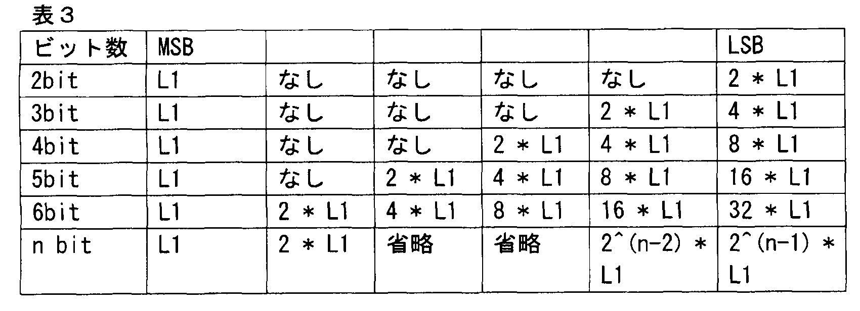
また、LSBに対応するインダクタ216のインダクタンスLを基準L1とした場合の設定例を表4に示す。
Table 4 shows a setting example when the inductance L of the inductor 216 corresponding to the LSB is set as the reference L1.
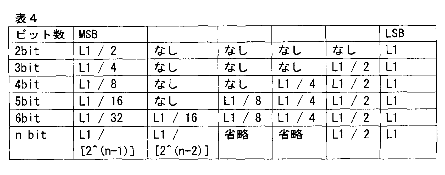
なお、表3および表4は、各インダクタ216のインダクタンスLを、2進数分割すなわち等分割に設定する例であるが、本発明はこれに限らず、不等分割で設定することもできる。その場合も、伝送信号のコーディング方法や信号のフォーマット、統計的な性質に応じた好適な分割幅を適宜選択すればよいが、一般的には下位ビットになるに従って、Lが大きくなるようにする。
Tables 3 and 4 are examples in which the inductance L of each inductor 216 is set to binary division, that is, equal division, but the present invention is not limited to this and can also be set to unequal division. In this case as well, a suitable division width may be selected as appropriate according to the coding method of the transmission signal, the signal format, and statistical properties. In general, L increases as the lower bits are used. .
本実施形態の信号合成回路200は、図15の構成に限らず、各種の変形が可能である。そこで、本実施形態の信号合成回路200の変形例を示す。
The signal synthesis circuit 200 according to the present embodiment is not limited to the configuration shown in FIG. Therefore, a modification of the signal synthesis circuit 200 of this embodiment is shown.
(2-1)変形例1
図16に、本実施形態の信号合成回路200の変形例1の構成を示す。 (2-1)Modification 1
FIG. 16 shows a configuration ofModification 1 of the signal synthesis circuit 200 of the present embodiment.
図16に、本実施形態の信号合成回路200の変形例1の構成を示す。 (2-1)
FIG. 16 shows a configuration of
図16に示すように、変形例1は、図15の構成と比較して、インダクタ216-1とキャパシタ217-1の位置を入れ替えると共に、インダクタ216-2とキャパシタ217-2の位置を入れ替えている。
As shown in FIG. 16, in the first modification, the positions of the inductor 216-1 and the capacitor 217-1 are interchanged and the positions of the inductor 216-2 and the capacitor 217-2 are interchanged as compared with the configuration of FIG. Yes.
変形例1の原理は、上述したブーシェロ回路の原理と同様である。
The principle of the first modification is the same as the principle of the above-described Bouchero circuit.
ここでは、図17に示すように、図14の構成に対して、インダクタ1002とキャパシタ1003の位置を入れ替えた回路について考える。
Here, as shown in FIG. 17, consider a circuit in which the positions of the inductor 1002 and the capacitor 1003 are exchanged with respect to the configuration of FIG.
図17の場合、負荷1004を流れる電流ILは、以下のように表される。
In the case of FIG. 17, the current IL flowing through the load 1004 is expressed as follows.

LC=1/(ω^2)のとき(すなわち、ω=ω0のとき)、電流ILは、負荷1004のRの大きさにかかわらず、IL=jωC・Vとなる。
When LC = 1 / (ω 2) (that is, when ω = ω 0 ), the current IL becomes IL = jωC · V regardless of the magnitude of R of the load 1004.
よって、LC=1/{(ω0)^2}のとき、図17の回路は、負荷1004に大きさILの電流源を接続した回路と等価になる。
Therefore, when LC = 1 / {(ω 0 ) ^ 2}, the circuit in FIG. 17 is equivalent to a circuit in which a current source having a magnitude IL is connected to the load 1004.
以上より、図16において、インダクタ216-1,216-2のインダクタンスをそれぞれL1,L2、キャパシタ217-1,217-2のキャパシタンスをそれぞれC1,C2とすると、変形例1の場合、L1・C1=L2・C2=1/{(ω0)^2}のとき、MSB側の電流I1は、j・ω・C1・Vdと比例関係にある。また、LSB側の電流I2は、j・ω・C2・Vdと比例関係にある。
From the above, in FIG. 16, assuming that the inductances of the inductors 216-1 and 216-2 are L1 and L2, respectively, and the capacitances of the capacitors 217-1 and 217-2 are C1 and C2, respectively, = L2 · C2 = 1 / {(ω 0 ) ^ 2}, the current I1 on the MSB side is proportional to j · ω · C1 · Vd. The current I2 on the LSB side is proportional to j · ω · C2 · Vd.
そのため、変形例1の場合、電圧から電流への電圧電流変換をする際の変換係数として、キャパシタ217-1,217-2のキャパシタンスC1,C2を互いに異ならせて、各ビットの信号に対する重み付けを行うことで、所望の電圧合成波形が得られる。例えば、図16においては、キャパシタ217-1のキャパシタンスをC1に、キャパシタ217-2のキャパシタンスC2を、C2=C1/2に設定している。
Therefore, in the case of the first modification, the capacitances C1 and C2 of the capacitors 217-1 and 217-2 are made different from each other as the conversion coefficients when performing the voltage-to-current conversion from voltage to current, and the signal for each bit is weighted. By doing so, a desired voltage composite waveform is obtained. For example, in FIG. 16, the capacitance of the capacitor 217-1 is set to C1, and the capacitance C2 of the capacitor 217-2 is set to C2 = C1 / 2.
なお、多ビットのデジタル送信信号に対する各キャパシタ217のキャパシタンスCは、表3や表4のように、2進数分割すなわち等分割に設定することもでき、また、不等分割で設定することもできる。その場合も、下位ビットになるに従って、Cが小さくなるようにする。
The capacitance C of each capacitor 217 for a multi-bit digital transmission signal can be set to binary division, that is, equal division, as shown in Tables 3 and 4, or can be set to unequal division. . Also in this case, C is made smaller as the lower bits are reached.
また、変形例1の場合も、フィルタ201-1,201-2で基本波以外の信号を反射させていることから、負荷300に対して基本波以外の信号が伝送されることはない。よって、送信増幅器の高効率化を図ることができると共に、スプリアス特性の改善を図ることもできる。その他の効果は図15と同様である。
Also, in the case of Modification 1, since signals other than the fundamental wave are reflected by the filters 201-1 and 201-2, a signal other than the fundamental wave is not transmitted to the load 300. Therefore, it is possible to improve the efficiency of the transmission amplifier and to improve the spurious characteristics. Other effects are the same as in FIG.
(2-2)変形例2
変形例2は、図15に示したLC集中定数回路を、2つの周波数に対応する2バンド化に拡張した例である。 (2-2)Modification 2
Modification 2 is an example in which the LC lumped constant circuit shown in FIG. 15 is expanded to two bands corresponding to two frequencies.
変形例2は、図15に示したLC集中定数回路を、2つの周波数に対応する2バンド化に拡張した例である。 (2-2)
変形例2の原理は、上述したブーシェロ回路の原理と同様である。
The principle of the modified example 2 is the same as that of the above-described Bouchero circuit.
ここでは、図18に示すように、電源1101と、LC並列共振回路1102と、LC直列共振回路1103と、負荷1104と、を有する回路について考える。
Here, as shown in FIG. 18, a circuit having a power source 1101, an LC parallel resonant circuit 1102, an LC series resonant circuit 1103, and a load 1104 is considered.
図18において、電源1001の電源電圧をV、LC並列共振回路1102を構成するインダクタのインダクタンスをL1、キャパシタのキャパシタンスをC1、LC並列共振回路1102全体のインピーダンスをZ1、LC直列共振回路1103を構成するインダクタのインダクタンスをL2、キャパシタのキャパシタンスをC2、LC直列共振回路1103全体のインピーダンスをZ2、負荷1104の抵抗をRL、負荷1104を流れる電流をILとすると、電流ILは、以下のように表される。
In FIG. 18, the power source voltage of the power source 1001 is V, the inductance of the inductor constituting the LC parallel resonant circuit 1102 is L 1 , the capacitance of the capacitor is C 1 , the impedance of the entire LC parallel resonant circuit 1102 is Z 1 , and the LC series resonant circuit. When the inductance of the inductor 1103 is L 2 , the capacitance of the capacitor is C 2 , the impedance of the entire LC series resonance circuit 1103 is Z 2 , the resistance of the load 1104 is R L , and the current flowing through the load 1104 is I L I L is expressed as follows:

ここで、sはラプラス演算子(=j・ω)で、簡単のため、
, Where s is the Laplace operator (= j · ω), for simplicity,

と置く(以下の図20において同じ)。
(Same in FIG. 20 below).
数式4の分母の第1項の()内が0になれば、数式4は負荷1104の抵抗RLに依存しない。そこで、数式4の分母の第1項の()内が0になるようなωの値を求める。このとき、ωとして2つの値が求められる。
If (1) in the first term of the denominator of Expression 4 is 0, Expression 4 does not depend on the resistance R L of the load 1104. Therefore, the value of ω is calculated so that the value in parentheses in the first term of the denominator of Equation 4 is zero. At this time, two values are obtained as ω.
ωが上記で求めた2つの値のいずれかの周波数である場合、数式4は、以下のように表すことができる。
When ω is one of the two values obtained above, Equation 4 can be expressed as follows.

したがって、電流ILは、負荷1104のRLに依存しない値となり、図18の回路は、負荷1104に大きさILの電流源を接続した回路と等価になる。
Therefore, the current I L becomes a value that does not depend on R L of the load 1104, and the circuit in FIG. 18 is equivalent to a circuit in which a current source having a magnitude I L is connected to the load 1104.
図19に、本実施形態の信号合成回路200の変形例2の構成を示す。なお、図19は、MSB側の構成のみを示しているが、LSB側の構成も同様である(以下の図21において同じ)。
FIG. 19 shows a configuration of Modification 2 of the signal synthesis circuit 200 of the present embodiment. FIG. 19 shows only the configuration on the MSB side, but the configuration on the LSB side is the same (the same applies to FIG. 21 below).
図19に示すように、変形例2は、図15の構成と比較して、インダクタ216-1の代わりに、LC並列共振回路218-1を設けると共に、キャパシタ217-1の代わりに、LC直列共振回路219-1を設けている。この構成の場合、LC並列共振回路218-1およびLC直列共振回路219-1で電圧電流変換部を構成している。
As shown in FIG. 19, in the second modification, an LC parallel resonant circuit 218-1 is provided instead of the inductor 216-1 and an LC series is used instead of the capacitor 217-1 as compared with the configuration of FIG. A resonance circuit 219-1 is provided. In this configuration, the LC parallel resonance circuit 218-1 and the LC series resonance circuit 219-1 constitute a voltage / current converter.
詳細には、スイッチモード増幅器100-1と合成点Xとの間の信号経路には、信号経路に直列にLC並列共振回路218-1が接続され、LC並列共振回路218-1の後段で信号経路に並列にLC直列共振回路219-1が接続されている。
Specifically, an LC parallel resonance circuit 218-1 is connected in series with the signal path between the switch mode amplifier 100-1 and the synthesis point X, and a signal is output at a stage subsequent to the LC parallel resonance circuit 218-1. An LC series resonance circuit 219-1 is connected in parallel with the path.
上述したブーシェロ回路の原理により、2つの周波数で、MSB側の電流I1およびLSB側の電流I2は、負荷300のRLに依存しない値となる。
The MSB-side current I1 and the LSB-side current I2 have values that do not depend on the RL of the load 300 at two frequencies according to the above-described principle of the Bushello circuit.
そのとき、2つの周波数で電圧電流変換を行うようにLC並列共振回路218-1およびLC直列共振回路219-1のインピーダンスを設定し、ω1・ω2=(ω0)^2とすることで、電流I1,I2を合成点Xにて電流合成することが可能である。
At that time, the impedances of the LC parallel resonance circuit 218-1 and the LC series resonance circuit 219-1 are set so as to perform voltage-current conversion at two frequencies, and ω 1 · ω 2 = (ω 0 ) ^ 2. Thus, the currents I1 and I2 can be synthesized at the synthesis point X.
このように、変形例2の場合、2つの周波数のそれぞれについて、スイッチモード増幅器100-1,100-2の出力信号を合成することができる。その他の効果は図15と同様である。
Thus, in the case of the modification 2, the output signals of the switch mode amplifiers 100-1 and 100-2 can be synthesized for each of the two frequencies. Other effects are the same as in FIG.
(2-3)変形例3
変形例3も、図15に示したLC集中定数回路を、2つの周波数に対応する2バンド化に拡張した例である。 (2-3)Modification 3
Modification 3 is also an example in which the LC lumped constant circuit shown in FIG. 15 is expanded to two bands corresponding to two frequencies.
変形例3も、図15に示したLC集中定数回路を、2つの周波数に対応する2バンド化に拡張した例である。 (2-3)
変形例3の原理は、上述したブーシェロ回路の原理と同様である。
The principle of the modification 3 is the same as the principle of the above-described Bouchero circuit.
ここでは、図20に示すように、電源1101と、LC直列共振回路1105と、LC並列共振回路1106と、負荷1104と、を有する回路について考える。
Here, as shown in FIG. 20, a circuit having a power source 1101, an LC series resonance circuit 1105, an LC parallel resonance circuit 1106, and a load 1104 is considered.
図20において、電源1001の電源電圧をV、LC直列共振回路1105を構成するインダクタのインダクタンスをL1、キャパシタのキャパシタンスをC1、LC直列共振回路1105全体のインピーダンスをZ1、LC並列共振回路1106を構成するインダクタのインダクタンスをL2、キャパシタのキャパシタンスをC2、LC並列共振回路1106全体のインピーダンスをZ2、負荷1104の抵抗をRL、負荷1104を流れる電流をILとすると、電流ILは、以下のように表される。
20, the power supply voltage of the power supply 1001 is V, the inductance of the inductor constituting the LC series resonance circuit 1105 is L 1 , the capacitance of the capacitor is C 1 , the impedance of the entire LC series resonance circuit 1105 is Z 1 , and the LC parallel resonance circuit Assuming that the inductance of the inductor constituting 1106 is L 2 , the capacitance of the capacitor is C 2 , the impedance of the entire LC parallel resonant circuit 1106 is Z 2 , the resistance of the load 1104 is R L , and the current flowing through the load 1104 is I L I L is expressed as follows:

数式7の分母の第1項の()内が0になれば、数式7は負荷1104の抵抗RLに依存しない。そこで、数式7の分母の第1項の()内が0になるようなωの値を求める。このとき、ωとして2つの値が求められる。
If (1) in the first term of the denominator of Expression 7 becomes 0, Expression 7 does not depend on the resistance R L of the load 1104. Therefore, the value of ω is calculated so that the value in parentheses in the first term of the denominator of Equation 7 is zero. At this time, two values are obtained as ω.
ωが上記で求めた2つの値のいずれかの周波数である場合、数式7は、以下のように表すことができる。
When ω is one of the two values obtained above, Equation 7 can be expressed as follows.

したがって、電流ILは、負荷1104のRLに依存しない値となり、図20の回路は、負荷1104に大きさILの電流源を接続した回路と等価になる。
Therefore, the current I L becomes a value that does not depend on R L of the load 1104, and the circuit of FIG. 20 is equivalent to a circuit in which a current source of magnitude I L is connected to the load 1104.
図21に、本実施形態の信号合成回路200の変形例3の構成を示す。
FIG. 21 shows a configuration of Modification 3 of the signal synthesis circuit 200 of the present embodiment.
図21に示すように、変形例3は、図15の構成と比較して、インダクタ216-1の代わりに、LC直列共振回路220-1を設けると共に、キャパシタ217-1の代わりに、LC並列共振回路221-1を設けている。この構成の場合、LC直列共振回路220-1およびLC並列共振回路221-1で電圧電流変換部を構成している。
As shown in FIG. 21, as compared with the configuration of FIG. 15, Modification 3 includes an LC series resonance circuit 220-1 instead of the inductor 216-1 and LC parallel instead of the capacitor 217-1. A resonance circuit 221-1 is provided. In this configuration, the LC series resonance circuit 220-1 and the LC parallel resonance circuit 221-1 constitute a voltage / current converter.
詳細には、スイッチモード増幅器100-1と合成点Xとの間の信号経路には、信号経路に直列にLC直列共振回路220-1が接続され、LC直列共振回路220-1の後段で信号経路に並列にLC並列共振回路221-1が接続されている。
More specifically, an LC series resonance circuit 220-1 is connected in series to the signal path between the switch mode amplifier 100-1 and the synthesis point X, and a signal is output after the LC series resonance circuit 220-1. An LC parallel resonant circuit 221-1 is connected in parallel with the path.
上述したブーシェロ回路の原理により、2つの周波数で、MSB側の電流I1およびLSB側の電流I2は、負荷300のRLに依存しない値となる。
The MSB-side current I1 and the LSB-side current I2 have values that do not depend on the RL of the load 300 at two frequencies according to the above-described principle of the Bushello circuit.
そのとき、2つの周波数で電圧電流変換を行うようにLC直列共振回路220-1およびLC並列共振回路221-1のインピーダンスを設定し、ω1・ω2=(ω0)^2とすることで、電流I1,I2を合成点Xにて電流合成することが可能である。
At that time, the impedances of the LC series resonance circuit 220-1 and the LC parallel resonance circuit 221-1 are set so as to perform voltage-current conversion at two frequencies, and ω 1 · ω 2 = (ω 0 ) ^ 2. Thus, the currents I1 and I2 can be synthesized at the synthesis point X.
このように、変形例3の場合、2つの周波数のそれぞれについて、スイッチモード増幅器100-1,100-2の出力信号を合成することができる。その他の効果は図15と同様である。
Thus, in the case of the modification 3, the output signals of the switch mode amplifiers 100-1 and 100-2 can be synthesized for each of the two frequencies. Other effects are the same as in FIG.
(2-4)その他の変形例
本実施形態の信号合成回路200は、上記以外にも各種の変形が可能である。 (2-4) Other Modifications Thesignal synthesis circuit 200 of the present embodiment can be variously modified in addition to the above.
本実施形態の信号合成回路200は、上記以外にも各種の変形が可能である。 (2-4) Other Modifications The
例えば、第1の実施形態の変形例1のように、各スイッチモード増幅器100と合成点Xとの間の信号経路において、LC集中定数回路の後段にフィルタ201を設けても良い。
For example, as in Modification 1 of the first embodiment, a filter 201 may be provided in the subsequent stage of the LC lumped constant circuit in the signal path between each switch mode amplifier 100 and the synthesis point X.
また、第1の実施形態の変形例2のように、フィルタ201を削除し、その代わりに、合成点Xと負荷300との間の信号経路にフィルタ203を設けても良い。
Further, as in Modification 2 of the first embodiment, the filter 201 may be deleted, and instead, the filter 203 may be provided in the signal path between the synthesis point X and the load 300.
上記の場合、フィルタ201の構成は、第1の実施形態で説明したものと同様にすることができる。
In the above case, the configuration of the filter 201 can be the same as that described in the first embodiment.
以上第1および第2の実施形態では、電圧電流変換部における電圧から電流への電圧電流変換をする際の変換係数を、インピーダンスが異なるように構成することにより、対応するビットに応じて重み付することで、電流I1,I2を重み付けしていた。
As described above, in the first and second embodiments, the conversion coefficient when performing voltage-to-current conversion from voltage to current in the voltage-to-current converter is configured so that the impedance is different, so that weighting is performed according to the corresponding bit. Thus, the currents I1 and I2 are weighted.
(3)第3の実施形態
本実施形態は、スイッチモード増幅器100-1,100-2の電源電圧を、対応するビットに応じて重み付することで、電流I1,I2を重み付けする。 (3) Third Embodiment In this embodiment, the currents I1 and I2 are weighted by weighting the power supply voltages of the switch mode amplifiers 100-1 and 100-2 according to the corresponding bits.
本実施形態は、スイッチモード増幅器100-1,100-2の電源電圧を、対応するビットに応じて重み付することで、電流I1,I2を重み付けする。 (3) Third Embodiment In this embodiment, the currents I1 and I2 are weighted by weighting the power supply voltages of the switch mode amplifiers 100-1 and 100-2 according to the corresponding bits.
図22に、本実施形態の信号合成回路200の基本構成を示す。
FIG. 22 shows a basic configuration of the signal synthesis circuit 200 of the present embodiment.
図22に示すように、本実施形態の信号合成回路200は、構成自体は図2と同様である。
As shown in FIG. 22, the signal synthesizing circuit 200 of this embodiment has the same configuration as that of FIG.
ただし、本実施形態の信号合成回路200は、スイッチモード増幅器100-1,100-2の電源電圧の電圧値が、互いに異なっており、対応するビットに応じて重み付けされている。
However, in the signal synthesis circuit 200 of this embodiment, the voltage values of the power supply voltages of the switch mode amplifiers 100-1 and 100-2 are different from each other, and are weighted according to the corresponding bits.
具体的には、図22においては、スイッチモード増幅器100-1の電源電圧をVdに、スイッチモード増幅器100-2の電源電圧をVd/2に設定している。
Specifically, in FIG. 22, the power supply voltage of the switch mode amplifier 100-1 is set to Vd, and the power supply voltage of the switch mode amplifier 100-2 is set to Vd / 2.
したがって、電流I1,I2は、スイッチモード増幅器100-1,100-2の電源電圧によってビットに応じて重み付けされている。よって、この電流I1,I2を合成点Xにて電流合成した電流IL(=I1+I2)を負荷300に供給することにより、所望の電圧合成波形が得られる。これにより、多ビットのデジタル送信信号を無線周波数で合成することができる。
Therefore, the currents I1 and I2 are weighted according to the bits by the power supply voltages of the switch mode amplifiers 100-1 and 100-2. Therefore, by supplying the current IL (= I1 + I2) obtained by synthesizing the currents I1 and I2 at the synthesis point X to the load 300, a desired voltage synthesis waveform can be obtained. Thereby, a multi-bit digital transmission signal can be synthesized at a radio frequency.
なお、本実施形態は、スイッチモード増幅器100-1,100-2の電源電圧を互いに異ならせるため、デジタル送信信号が2ビットの場合、2種類の電源が必要となり、第1および第2の実施形態と比較すると、電源の種類が多くなる。
In this embodiment, since the power supply voltages of the switch mode amplifiers 100-1 and 100-2 are different from each other, when the digital transmission signal is 2 bits, two types of power supplies are required. Compared with the form, there are more types of power supplies.
また、基本波以外の信号は、フィルタ201-1,201-2で反射させられるため、負荷300に伝送されることはない。よって、送信増幅器の高効率化を図ることができる。また、負荷300から見ると、高調波が減衰するため、スプリアス特性の改善を図ることもできる。
In addition, since signals other than the fundamental wave are reflected by the filters 201-1 and 201-2, they are not transmitted to the load 300. Therefore, the efficiency of the transmission amplifier can be increased. Further, since the harmonics are attenuated when viewed from the load 300, the spurious characteristics can be improved.
また、1/4波長伝送線路トランス202-1,202-2の特性インピーダンスを同一にできるため、1/4波長伝送線路トランス202-1,202-2を共通に設計することができる。
Further, since the characteristic impedances of the quarter wavelength transmission line transformers 202-1 and 202-2 can be made the same, the quarter wavelength transmission line transformers 202-1 and 202-2 can be designed in common.
また、合成点Xの前段の基本波近傍でのインピーダンスは、スイッチモード増幅器100-1,100-2のスイッチ素子のON/OFF時に確定し、スイッチ素子の状態によらずにスイッチモード増幅器100-1,100-2の出力では高周波的にインピーダンスが低いので電圧源とみなすことができるから、後段に接続される1/4波長伝送線路トランス202-1,202-2の電圧-電流変換作用により、信号合成回路200は、電流I1の電流源と電流I2の電流源とが合成点Xに接続された回路と等価になる。よって、合成点Xの各ポートにおいて、他のポートとのアイソレーションを取ることができる。
Further, the impedance in the vicinity of the fundamental wave at the preceding stage of the synthesis point X is determined when the switch elements of the switch mode amplifiers 100-1 and 100-2 are turned on / off, and the switch mode amplifier 100- regardless of the state of the switch elements. Since the output of 1,100-2 has a low impedance in terms of high frequency, it can be regarded as a voltage source. The signal synthesis circuit 200 is equivalent to a circuit in which a current source of current I1 and a current source of current I2 are connected to the synthesis point X. Therefore, each port at the synthesis point X can be isolated from other ports.
なお、本実施形態においては、デジタル送信信号が2ビットであると仮定しているが、本発明はこれに限らず、多ビットのデジタル送信信号に対応可能である。
In the present embodiment, it is assumed that the digital transmission signal is 2 bits. However, the present invention is not limited to this, and can accommodate a multi-bit digital transmission signal.
ここで、1/4波長伝送線路トランス202の特性インピーダンスを全て同一とし、MBSに対応するスイッチモード増幅器100の電源電圧を基準Vdとした場合において、多ビットのデジタル送信信号に対する各スイッチモード増幅器100の電源電圧の設定例を表5に示す。
Here, when all the characteristic impedances of the ¼ wavelength transmission line transformer 202 are the same and the power supply voltage of the switch mode amplifier 100 corresponding to MBS is the reference Vd, each switch mode amplifier 100 for a multi-bit digital transmission signal is used. Table 5 shows an example of setting the power supply voltage.

LSBに対応するスイッチモード増幅器100の電源電圧を基準Vdとした場合の設定例は説明を省略する。
Description of the setting example when the power supply voltage of the switch mode amplifier 100 corresponding to the LSB is the reference Vd will be omitted.
なお、表5は、各スイッチモード増幅器100の電源電圧を、2進数分割すなわち等分割に設定する例であるが、本発明はこれに限らず、不等分割で設定することもできる。その場合も、伝送信号のコーディング方法や信号のフォーマット、統計的な性質に応じた好適な分割幅を適宜選択すればよいが、一般的には下位ビットになるに従って、電源電圧が小さくなるようにする。
Table 5 is an example in which the power supply voltage of each switch mode amplifier 100 is set to binary division, that is, equal division, but the present invention is not limited to this, and can be set by unequal division. In this case as well, a suitable division width may be selected as appropriate according to the coding method of the transmission signal, the signal format, and the statistical properties. In general, the power supply voltage decreases as the lower bits are used. To do.
本実施形態の信号合成回路200は、電圧電流変換部として、第1の実施形態の1/4波長伝送線路トランスを用いた構成を例に挙げたが、第2の実施形態のLC集中定数回路を用いた構成にも適用可能である。
In the signal synthesis circuit 200 of the present embodiment, the configuration using the quarter wavelength transmission line transformer of the first embodiment as the voltage-current converter is taken as an example, but the LC lumped constant circuit of the second embodiment is used. The present invention can also be applied to a configuration using.
また、本実施形態の信号合成回路200は、第1および第2の実施形態の各変形例の構成にも適用可能である。
Further, the signal synthesis circuit 200 of the present embodiment can also be applied to the configurations of the modified examples of the first and second embodiments.
(4)第4の実施形態
第1および第2の実施形態は、電圧電流変換部における電圧から電流への電圧電流変換をする際の変換係数を、対応するビットに応じて重み付することで、電流I1,I2を重み付けしていた。 (4) Fourth Embodiment In the first and second embodiments, the conversion coefficient when performing voltage-current conversion from voltage to current in the voltage-current converter is weighted according to the corresponding bit. The currents I1 and I2 are weighted.
第1および第2の実施形態は、電圧電流変換部における電圧から電流への電圧電流変換をする際の変換係数を、対応するビットに応じて重み付することで、電流I1,I2を重み付けしていた。 (4) Fourth Embodiment In the first and second embodiments, the conversion coefficient when performing voltage-current conversion from voltage to current in the voltage-current converter is weighted according to the corresponding bit. The currents I1 and I2 are weighted.
これに対して、本実施形態は、スイッチモード増幅器100-1,100-2の入力信号(パルス波形信号)におけるパルスの間引き率を、対応するビットに応じて重み付することで、電流I1,I2を重み付けする。
On the other hand, in this embodiment, the current I1, I2 is weighted by weighting the pulse thinning rate in the input signals (pulse waveform signals) of the switch mode amplifiers 100-1 and 100-2 according to the corresponding bits. Weight I2.
図23に、本実施形態の信号合成回路200の基本構成を示す。
FIG. 23 shows a basic configuration of the signal synthesis circuit 200 of the present embodiment.
図23に示すように、本実施形態の信号合成回路200は、構成自体は図2と同様である。
As shown in FIG. 23, the signal synthesis circuit 200 of the present embodiment has the same configuration as that of FIG.
ただし、本実施形態の信号合成回路200は、スイッチモード増幅器100-1,100-2の入力信号におけるパルスの間引き率が、互いに異なっており、対応するビットに応じて重み付けされている。
However, in the signal synthesis circuit 200 of this embodiment, the pulse decimation rates in the input signals of the switch mode amplifiers 100-1 and 100-2 are different from each other, and are weighted according to the corresponding bits.
具体的には、図23においては、スイッチモード増幅器100-2の入力信号におけるパルスの間引き率を、スイッチモード増幅器100-1の入力信号におけるパルスの間引き率よりも大きく設定する。
Specifically, in FIG. 23, the pulse thinning rate in the input signal of the switch mode amplifier 100-2 is set larger than the pulse thinning rate in the input signal of the switch mode amplifier 100-1.
本実施形態においては、図24に示すように、パルスの間引き率をパルス間隔で規定することを考える。このとき、パルス幅はTc/2で一定とする。この場合、スイッチモード増幅器100-1の入力信号におけるパルスのパルス間隔はTc、スイッチモード増幅器100-2の入力信号におけるパルスのパルス間隔は2*Tcとなる。
In the present embodiment, as shown in FIG. 24, it is considered that the pulse thinning rate is defined by the pulse interval. At this time, the pulse width is constant at Tc / 2. In this case, the pulse interval of the pulse in the input signal of the switch mode amplifier 100-1 is Tc, and the pulse interval of the pulse in the input signal of the switch mode amplifier 100-2 is 2 * Tc.
図24において、矩形波は、入力信号のパルスの波形を表し、正弦波は、そのパルスに含まれる所望の周波数成分の波形を表している。所望の周波数成分の波形に着目すると、その振幅は、パルス間隔(すなわち、間引き率)に応じて変化し、重み付けされていることがわかる。
24, a rectangular wave represents a waveform of a pulse of an input signal, and a sine wave represents a waveform of a desired frequency component included in the pulse. Focusing on the waveform of the desired frequency component, it can be seen that the amplitude changes according to the pulse interval (that is, the thinning rate) and is weighted.
したがって、電流I1,I2は、スイッチモード増幅器100-1,100-2の入力信号におけるパルスの間引き率によってビットに応じて重み付けされている。よって、この電流I1,I2を合成点Xにて電流合成した電流IL(=I1+I2)を負荷300に供給することにより、所望の電圧合成波形が得られる。これにより、多ビットのデジタル送信信号を無線周波数で合成することができる。
Therefore, the currents I1 and I2 are weighted according to the bit by the thinning rate of the pulses in the input signals of the switch mode amplifiers 100-1 and 100-2. Therefore, by supplying the current IL (= I1 + I2) obtained by synthesizing the currents I1 and I2 at the synthesis point X to the load 300, a desired voltage synthesis waveform can be obtained. Thereby, a multi-bit digital transmission signal can be synthesized at a radio frequency.
また、スイッチモード増幅器100-1,100-2の電源電圧を同じ種類とすることができるため、電源回路の簡素化および低コスト化を図ることができる。
Further, since the power supply voltages of the switch mode amplifiers 100-1 and 100-2 can be of the same type, the power supply circuit can be simplified and the cost can be reduced.
また、1/4波長伝送線路トランス202-1,202-2の特性インピーダンスを同一にできるため、1/4波長伝送線路トランス202-1,202-2を共通に設計することができる。
Further, since the characteristic impedances of the quarter wavelength transmission line transformers 202-1 and 202-2 can be made the same, the quarter wavelength transmission line transformers 202-1 and 202-2 can be designed in common.
また、基本波以外の信号は、フィルタ201-1,201-2で反射させられるため、負荷300に伝送されることはない。よって、送信増幅器の高効率化を図ることができる。また、負荷300から見ると、高調波が減衰するため、スプリアス特性の改善を図ることもできる。
In addition, since signals other than the fundamental wave are reflected by the filters 201-1 and 201-2, they are not transmitted to the load 300. Therefore, the efficiency of the transmission amplifier can be increased. Further, since the harmonics are attenuated when viewed from the load 300, the spurious characteristics can be improved.
また、合成点Xの前段の基本波近傍でのインピーダンスは、スイッチモード増幅器100-1,100-2のスイッチ素子のON/OFF時に確定し、スイッチ素子の状態によらずにスイッチモード増幅器100-1,100-2の出力では高周波的にインピーダンスが低いので電圧源とみなすことができるから、後段に接続される1/4波長伝送線路トランス202-1,202-2の電圧-電流変換作用により、信号合成回路200は、電流I1の電流源と電流I2の電流源とが合成点Xに接続された回路と等価になる。よって、合成点Xの各ポートにおいて、他のポートとのアイソレーションを取ることができる。
Further, the impedance in the vicinity of the fundamental wave at the preceding stage of the synthesis point X is determined when the switch elements of the switch mode amplifiers 100-1 and 100-2 are turned on / off, and the switch mode amplifier 100- regardless of the state of the switch elements. Since the output of 1,100-2 has a low impedance in terms of high frequency, it can be regarded as a voltage source. The signal synthesis circuit 200 is equivalent to a circuit in which a current source of current I1 and a current source of current I2 are connected to the synthesis point X. Therefore, each port at the synthesis point X can be isolated from other ports.
なお、本実施形態においては、デジタル送信信号が2ビットであると仮定しているが、本発明はこれに限らず、多ビットのデジタル送信信号に対応可能である。
In the present embodiment, it is assumed that the digital transmission signal is 2 bits. However, the present invention is not limited to this, and can accommodate a multi-bit digital transmission signal.
ここで、スイッチモード増幅器100の電源電圧を全て同一、かつ、1/4波長伝送線路トランス202の特性インピーダンスを全て同一とし、MBSに対応するスイッチモード増幅器100の入力信号におけるパルスのパルス間隔を基準Tcとした場合において、多ビットのデジタル送信信号に対する各スイッチモード増幅器100の入力信号におけるパルスのパルス間隔の設定例を表6に示す。また、図25に、表6のようにパルス間隔に設定したパルスの一部を示す。
Here, the power supply voltages of the switch mode amplifier 100 are all the same, the characteristic impedances of the quarter wavelength transmission line transformer 202 are all the same, and the pulse interval of pulses in the input signal of the switch mode amplifier 100 corresponding to MBS is used as a reference. Table 6 shows a setting example of the pulse interval of the pulse in the input signal of each switch mode amplifier 100 with respect to the multi-bit digital transmission signal when Tc is set. FIG. 25 shows a part of the pulses set at the pulse interval as shown in Table 6.

LSBに対応するスイッチモード増幅器100の入力信号におけるパルスのパルス間隔を基準Tcとした場合の設定例は説明を省略する。
Description of the setting example when the pulse interval of the pulse in the input signal of the switch mode amplifier 100 corresponding to the LSB is the reference Tc will be omitted.
なお、表6は、各スイッチモード増幅器100の入力信号におけるパルスのパルス間隔を、2進数分割すなわち等分割に設定する例であるが、本発明はこれに限らず、不等分割で設定することもできる。その場合も、伝送信号のコーディング方法や信号のフォーマット、統計的な性質に応じた好適な分割幅を適宜選択すればよいが、一般的には下位ビットになるに従って、パルス間隔が大きく(すなわち、間引き率が大きく)なるようにする。
Table 6 is an example in which the pulse interval of the input signal of each switch mode amplifier 100 is set to binary division, that is, equal division, but the present invention is not limited to this, and is set by unequal division. You can also. Even in this case, a suitable division width may be appropriately selected according to the coding method of the transmission signal, the signal format, and the statistical properties, but generally the pulse interval increases as the lower bits (that is, (Thinning rate is large).
本実施形態の信号合成回路200は、電圧電流変換部として、第1の実施形態の1/4波長伝送線路トランスを用いた構成を例に挙げたが、第2の実施形態のLC集中定数回路を用いた構成にも適用可能である。
In the signal synthesis circuit 200 of the present embodiment, the configuration using the quarter wavelength transmission line transformer of the first embodiment as the voltage-current converter is taken as an example, but the LC lumped constant circuit of the second embodiment is used. The present invention can also be applied to a configuration using.
また、本実施形態の信号合成回路200は、第1および第2の実施形態の各変形例の構成にも適用可能である。
Further, the signal synthesis circuit 200 of the present embodiment can also be applied to the configurations of the modified examples of the first and second embodiments.
なお、第3および第4の実施形態は、電流I1,I2の重み付け方法(第3の実施形態では電源電圧で、第4の実施形態ではパルスの間引き率で重み付けする)が異なるものの、信号合成回路200の構成自体は同一である。そのため、共通して同じ設計の信号合成回路200を適用して、第3および第4の実施形態の両方の重み付け方法に対応することができる。この点でも設計や回路の共通利用に寄与するという更なる効果を奏する。
The third and fourth embodiments differ in the weighting method of the currents I1 and I2 (weighting with the power supply voltage in the third embodiment and weighting with the pulse thinning rate in the fourth embodiment), but the signal synthesis. The configuration itself of the circuit 200 is the same. Therefore, it is possible to deal with both the weighting methods of the third and fourth embodiments by applying the signal synthesis circuit 200 having the same design in common. This also brings about the further effect of contributing to the common use of design and circuits.
(5)第5の実施形態
本実施形態は、第4の実施形態の変形例であり、スイッチモード増幅器100-1,100-2の出力電力を、スイッチモード増幅器100-1,100-2の入力信号におけるパルスの間引き率により制御する。 (5) Fifth Embodiment This embodiment is a modification of the fourth embodiment, in which the output power of the switch mode amplifiers 100-1 and 100-2 is changed to that of the switch mode amplifiers 100-1 and 100-2. It is controlled by the thinning rate of pulses in the input signal.
本実施形態は、第4の実施形態の変形例であり、スイッチモード増幅器100-1,100-2の出力電力を、スイッチモード増幅器100-1,100-2の入力信号におけるパルスの間引き率により制御する。 (5) Fifth Embodiment This embodiment is a modification of the fourth embodiment, in which the output power of the switch mode amplifiers 100-1 and 100-2 is changed to that of the switch mode amplifiers 100-1 and 100-2. It is controlled by the thinning rate of pulses in the input signal.
具体的には、図26に示すように、出力電力に応じて、MSB側のスイッチモード増幅器100-1のみにパルスを入力する領域(出力電力が所定値以下の低出力動作時:図26の例では(a)~(c))と、LSB側のスイッチモード増幅器100-2にもパルスを入力する領域(出力電力が所定値を超える高出力動作時:図26の例では(d)~(f))と、に分けている。
Specifically, as shown in FIG. 26, a region in which a pulse is input only to the switch mode amplifier 100-1 on the MSB side according to the output power (during low output operation where the output power is a predetermined value or less: FIG. In the example, (a) to (c)) and a region where a pulse is also input to the switch mode amplifier 100-2 on the LSB side (during high output operation where the output power exceeds a predetermined value: (d) to (d) in the example of FIG. (F)).
さらに、低出力動作時には、MSB側のスイッチモード増幅器100-1に入力するパルスの間引き率を出力電力に応じて制御する(出力電力が大きいほど、間引き率が小さくなるように制御する)。
Furthermore, at the time of low output operation, the thinning rate of pulses input to the switch mode amplifier 100-1 on the MSB side is controlled according to the output power (control is performed so that the thinning rate decreases as the output power increases).
また、高出力動作時には、MSB側のスイッチモード増幅器100-1に入力するパルスの間引き率は固定し、LSB側のスイッチモード増幅器100-2に入力するパルスの間引き率を出力電力に応じて制御する(出力電力が大きいほど、間引き率が小さくなるように制御する)。
During high output operation, the thinning rate of pulses input to the MSB side switch mode amplifier 100-1 is fixed, and the thinning rate of pulses input to the LSB side switch mode amplifier 100-2 is controlled according to the output power. (Control is performed so that the thinning rate decreases as the output power increases).
本実施形態の効果を、図7の構成の場合における合成点Xでの2ビット合成の信号波形を例に挙げて説明する。スイッチモード増幅器100-1,100-2の出力信号は電圧電流変換されているため、合成点Xにおいて、スイッチモード増幅器100-1,100-2は、等価的に独立な電流源の並列接続となり、スイッチモード増幅器100-1,100-2の出力信号のパルスは互いに独立に足し合わされる。そのため、供給タイミングをずらすことで、各種間引き率に応じて多様な重み付けが可能となり、図26の入力信号例では、合成点Xにて図26の出力パルス波形が得られる。なお、本実施形態の効果を理解しやすく説明する便宜上、図26の出力パルス波形には、スイッチモード増幅器100-1,100-2から合成点Xに至るフィルタ201-1,201-2にて出力パルスが帯域制限を受けて、パルスに含まれる基本波成分が取り出されたのち合成される様子は示していない。しかし、図24もしくは図25に示したパルスと基本波成分の関係から、図26の出力パルス波形に含まれる2ビット合成後の基本波波形を得ることができる。
The effect of this embodiment will be described with reference to an example of a signal waveform of 2-bit synthesis at the synthesis point X in the case of the configuration of FIG. Since the output signals of the switch mode amplifiers 100-1 and 100-2 are voltage-current converted, the switch mode amplifiers 100-1 and 100-2 are equivalently connected in parallel with independent current sources at the synthesis point X. The pulses of the output signals of the switch mode amplifiers 100-1 and 100-2 are added independently of each other. Therefore, by shifting the supply timing, various weighting can be performed according to various thinning rates. In the example of the input signal in FIG. 26, the output pulse waveform in FIG. For convenience of understanding and explaining the effect of the present embodiment, the output pulse waveform of FIG. 26 is obtained by the filters 201-1 and 201-2 from the switch mode amplifiers 100-1 and 100-2 to the synthesis point X. It is not shown how the output pulse is subjected to band limitation and synthesized after the fundamental wave component included in the pulse is extracted. However, from the relationship between the pulse and the fundamental wave component shown in FIG. 24 or FIG. 25, the fundamental wave waveform after 2-bit synthesis included in the output pulse waveform of FIG. 26 can be obtained.
したがって、本実施形態においても、第4の実施形態と同様に電流I1,I2を重み付けすることができるため、第4の実施形態と同様の効果が得られる。
Therefore, also in this embodiment, since the currents I1 and I2 can be weighted similarly to the fourth embodiment, the same effect as the fourth embodiment can be obtained.
また、本実施形態においては、2つのスイッチモード増幅器100-1,100-2に異なる間引き率のパルスを入力しているため(差異コード入力)、図27の出力・効率曲線に示すように、2つのスイッチモード増幅器100-1,100-2に同一の間引き率のパルスを入力する構成(同一コード入力)と比較して、低出力動作時(バックオフ動作)にも高効率で動作することができるという効果が得られる。
In the present embodiment, since pulses with different thinning rates are input to the two switch mode amplifiers 100-1 and 100-2 (difference code input), as shown in the output / efficiency curve of FIG. Compared to the configuration in which pulses with the same decimation rate are input to the two switch mode amplifiers 100-1 and 100-2 (same code input), the switch mode amplifiers 100-1 and 100-2 operate with higher efficiency even during low output operation (backoff operation). The effect of being able to be obtained.
また、本実施形態においては、第3の実施形態と同様にMSB側の電源電圧を異ならせる構成と組み合わせれば、図28の出力・効率曲線に示すように、バックオフ動作の効率ピークポイントを、回路などの物理的な修正を要さずに容易に制御することも可能という、さらなる効果が得られる。
Further, in this embodiment, when combined with a configuration in which the power supply voltage on the MSB side is made different as in the third embodiment, the efficiency peak point of the back-off operation is obtained as shown in the output / efficiency curve of FIG. Furthermore, it is possible to easily control without requiring physical modification of a circuit or the like.
また、本実施形態においても、第4の実施形態で述べたような構成への対応(2ビット以外のビットへの対応等)が可能である。
Also in this embodiment, it is possible to cope with the configuration as described in the fourth embodiment (corresponding to bits other than 2 bits).
以上、実施形態を参照して本発明を説明したが、本発明は上記実施形態に限定されるものではない。本発明の構成や詳細には、本発明の範囲内で当業者が理解し得る様々な変更をすることができる。
The present invention has been described above with reference to the embodiments, but the present invention is not limited to the above embodiments. Various changes that can be understood by those skilled in the art can be made to the configuration and details of the present invention within the scope of the present invention.
例えば、上記実施形態においては、デジタル送信信号が2ビットであると仮定したが、本発明はこれに限らず、多ビットのデジタル送信信号に対応が可能である。
For example, in the above-described embodiment, it is assumed that the digital transmission signal is 2 bits. However, the present invention is not limited to this, and can handle a multi-bit digital transmission signal.
また、上記実施形態においては、電圧電流変換部と帯域制限部を2バンド化に拡張した例について説明したが、本発明はこれに限らず、電圧電流変換部と帯域制限部を構成する素子数を増やすことにより、さらなる複数バンド化への拡張にも対応可能である。また電圧電流変換部として1/4波長伝送線路トランスと集中定数型を組み合わせて信号合成回路を構成することが可能であることも理解できるであろう。
Moreover, in the said embodiment, although the example which expanded the voltage current conversion part and the band limitation part to 2 bands was demonstrated, this invention is not restricted to this, The number of the elements which comprise a voltage current conversion part and a band limitation part By increasing the number, it is possible to cope with further expansion to multiple bands. It will also be understood that a signal synthesis circuit can be configured by combining a quarter wavelength transmission line transformer and a lumped constant type as a voltage-current converter.
さらには、上記実施形態においては、1/4波長伝送線路トランスや集中定数素子さらにはスイッチモード増幅器は、理想的な特性を備えたものとして多ビット信号を合成する動作や効果について説明している。しかし、現実に用いる素子によってはそれらの寄生成分を補償したり、電圧波形や電流波形の位相をより理想的な信号合成動作に近づけるための線路形状や素子値の変更さらには補償用素子の追加を行うなどの変更も可能であろう。
Furthermore, in the above-described embodiment, the quarter wavelength transmission line transformer, the lumped constant element, and the switch mode amplifier are described as having the ideal characteristics and the operation and effect of synthesizing a multi-bit signal. . However, depending on the elements used in practice, the parasitic components can be compensated, the line shape and element values can be changed to make the phase of the voltage waveform and current waveform closer to ideal signal synthesis operations, and compensation elements have been added. It is possible to make changes such as
本出願は、2012年9月14日に出願された日本出願特願2012-202591および2013年2月4日に出願された日本出願特願2013-019538を基礎とする優先権を主張し、その開示の全てをここに取り込む。
This application claims priority based on Japanese Patent Application No. 2012-202591 filed on September 14, 2012 and Japanese Patent Application No. 2013-019538 filed on February 4, 2013, The entire disclosure is incorporated herein.
100-1,100-2 スイッチモード増幅器
200 信号合成回路
201-1,201-2 フィルタ
202-1,202-2 1/4波長伝送線路トランス
203 フィルタ
204-1 伝送線路トランス
205-1,206-1 オープンスタブ
207-1,208-1 伝送線路トランス
209-1 オープンスタブ
210-1 伝送線路トランス
211-1,212-1 ショートスタブ
213-1,214-1 伝送線路トランス
215-1 ショートスタブ
216-1,216-2 インダクタ
217-1,217-2 キャパシタ
218-1 LC並列共振回路
219-1 LC直列共振回路
220-1 LC直列共振回路
221-1 LC並列共振回路
300 負荷
X 合成点
410 デジタルベースバンド信号生成部
420 変調回路
421 IQモジュレータ
422 変換器
423 変調器
424 積算器
425 デコーダ 100-1, 100-2switch mode amplifier 200 signal synthesis circuit 201-1 and 201-2 filter 202-1 and 202-2 quarter wavelength transmission line transformer 203 filter 204-1 transmission line transformer 205-1 and 206- 1 Open Stub 207-1, 208-1 Transmission Line Transformer 209-1 Open Stub 210-1 Transmission Line Transformer 211-1, 212-1 Short Stub 213-1, 214-1 Transmission Line Transformer 215-1 Short Stub 216- DESCRIPTION OF SYMBOLS 1,216-2 Inductor 217-1,217-2 Capacitor 218-1 LC parallel resonance circuit 219-1 LC series resonance circuit 220-1 LC series resonance circuit 221-1 LC parallel resonance circuit 300 Load X Composite point 410 Digital base Band signal generator 20 modulation circuit 421 IQ modulator 422 converter 423 Modulator 424 integrator 425 decoder
200 信号合成回路
201-1,201-2 フィルタ
202-1,202-2 1/4波長伝送線路トランス
203 フィルタ
204-1 伝送線路トランス
205-1,206-1 オープンスタブ
207-1,208-1 伝送線路トランス
209-1 オープンスタブ
210-1 伝送線路トランス
211-1,212-1 ショートスタブ
213-1,214-1 伝送線路トランス
215-1 ショートスタブ
216-1,216-2 インダクタ
217-1,217-2 キャパシタ
218-1 LC並列共振回路
219-1 LC直列共振回路
220-1 LC直列共振回路
221-1 LC並列共振回路
300 負荷
X 合成点
410 デジタルベースバンド信号生成部
420 変調回路
421 IQモジュレータ
422 変換器
423 変調器
424 積算器
425 デコーダ 100-1, 100-2
Claims (31)
- ベースバンド信号を無線周波数帯の成分を含む多ビットデジタル信号に変調する変調回路と、
前記変調回路から出力された前記多ビットデジタル信号の各ビットに対応して設けられた複数のスイッチモード増幅器と、
前記複数のスイッチモード増幅器の出力信号を帯域制限する帯域制限部と、前記スイッチモード増幅器の出力信号を電圧から電流に変換する電圧電流変換部と、を接続して信号合成する信号合成回路と、
を有する送信機。 A modulation circuit that modulates a baseband signal into a multi-bit digital signal including components of a radio frequency band;
A plurality of switch mode amplifiers provided corresponding to each bit of the multi-bit digital signal output from the modulation circuit;
A signal synthesizing circuit that synthesizes a signal by connecting a band limiting unit that limits a band of the output signals of the plurality of switch mode amplifiers, and a voltage / current converting unit that converts the output signals of the switch mode amplifier from voltage to current;
Having a transmitter. - 前記電圧電流変換部は、前記各ビットに対応してインピーダンスが異なる、請求項1に記載の送信機。 The transmitter according to claim 1, wherein the voltage-current converter has different impedance corresponding to each bit.
- 前記スイッチモード増幅器の電源電圧は、前記各ビットに対応して電圧値が異なる、請求項1に記載の送信機。 The transmitter according to claim 1, wherein the power voltage of the switch mode amplifier has a voltage value corresponding to each bit.
- 前記スイッチモード増幅器の入力信号におけるパルスは、前記各ビットに対応して間引き率が異なる、請求項1に記載の送信機。 The transmitter according to claim 1, wherein the pulse in the input signal of the switch mode amplifier has a different thinning rate corresponding to each bit.
- 前記スイッチモード増幅器の出力電力を、前記スイッチモード増幅器の入力信号におけるパルスの間引き率により制御し、
前記出力電力が所定値以下の場合は、前記スイッチモード増幅器の一部のみに当該パルスを入力し、当該一部のスイッチモード増幅器への当該パルスは出力電力に応じて間引き率を制御し、
前記出力電力が所定値を超える場合には、前記スイッチモード増幅器の一部は当該パルスの間引き率を固定し、その他のスイッチモード増幅器への当該パルスは出力電力に応じて間引き率を制御する、請求項1に記載の送信機。 The output power of the switch mode amplifier is controlled by the thinning rate of pulses in the input signal of the switch mode amplifier,
When the output power is a predetermined value or less, the pulse is input only to a part of the switch mode amplifier, the pulse to the part of the switch mode amplifier controls the thinning rate according to the output power,
When the output power exceeds a predetermined value, a part of the switch mode amplifier fixes the thinning rate of the pulse, and the pulse to the other switch mode amplifier controls the thinning rate according to the output power. The transmitter according to claim 1. - 前記帯域制限部および前記電圧電流変換部は、
前記複数のスイッチモード増幅器と合成点との間の複数の第1信号経路の各々に設けられており、
前記帯域制限部は、
前記電圧電流変換部の前段に設けられており、
LC直列共振回路から構成される、請求項1から5のいずれか1項に記載の送信機。 The band limiting unit and the voltage-current conversion unit are:
Provided in each of a plurality of first signal paths between the plurality of switch mode amplifiers and a synthesis point;
The band limiting unit includes:
Provided in the previous stage of the voltage-current converter,
The transmitter according to any one of claims 1 to 5, comprising an LC series resonance circuit. - 前記帯域制限部および前記電圧電流変換部は、
前記複数のスイッチモード増幅器と合成点との間の複数の第1信号経路の各々に設けられており、
前記帯域制限部は、
前記電圧電流変換部の後段に設けられており、
LC並列共振回路から構成される、請求項1から5のいずれか1項に記載の送信機。 The band limiting unit and the voltage-current conversion unit are:
Provided in each of a plurality of first signal paths between the plurality of switch mode amplifiers and a synthesis point;
The band limiting unit includes:
Provided in the subsequent stage of the voltage-current converter,
The transmitter according to any one of claims 1 to 5, comprising an LC parallel resonant circuit. - 前記帯域制限部および前記電圧電流変換部は、
前記複数のスイッチモード増幅器と合成点との間の複数の第1信号経路の各々に設けられており、
前記帯域制限部は、
前記電圧電流変換部の後段に設けられており、
前記第1信号経路に直列に接続されたLC直列共振回路と、
前記LC直列共振回路の前段で、前記第1信号経路に並列に接続されたLC並列共振回路およびキャパシタと、から構成される、請求項1から5のいずれか1項に記載の送信機。 The band limiting unit and the voltage-current conversion unit are:
Provided in each of a plurality of first signal paths between the plurality of switch mode amplifiers and a synthesis point;
The band limiting unit includes:
Provided in the subsequent stage of the voltage-current converter,
An LC series resonant circuit connected in series to the first signal path;
The transmitter according to any one of claims 1 to 5, comprising an LC parallel resonant circuit and a capacitor connected in parallel to the first signal path in a stage preceding the LC series resonant circuit. - 前記電圧電流変換部は、
前記複数のスイッチモード増幅器と合成点との間の複数の第1信号経路の各々に設けられており、
前記帯域制限部は、
前記合成点と負荷との間の第2信号経路に設けられており、
前記帯域制限部は、
LC並列共振回路から構成される、請求項1から5のいずれか1項に記載の送信機。 The voltage-current converter is
Provided in each of a plurality of first signal paths between the plurality of switch mode amplifiers and a synthesis point;
The band limiting unit includes:
Provided in a second signal path between the synthesis point and the load;
The band limiting unit includes:
The transmitter according to any one of claims 1 to 5, comprising an LC parallel resonant circuit. - 前記電圧電流変換部は、前記第1信号経路に直列に接続された1/4波長伝送線路トランスから構成される、請求項6から9のいずれか1項に記載の送信機。 The transmitter according to any one of claims 6 to 9, wherein the voltage-current converter is configured by a ¼ wavelength transmission line transformer connected in series to the first signal path.
- 前記電圧電流変換部は、
前記第1信号経路に直列に接続されたインダクタと、
前記インダクタの後段で前記第1信号経路に並列に接続されたキャパシタと、から構成される、請求項6から9のいずれか1項に記載の送信機。 The voltage-current converter is
An inductor connected in series to the first signal path;
The transmitter according to claim 6, further comprising a capacitor connected in parallel to the first signal path at a subsequent stage of the inductor. - 前記電圧電流変換部は、
前記第1信号経路に直列に接続されたキャパシタと、
前記キャパシタの後段で前記第1信号経路に並列に接続されたインダクタと、から構成される、請求項6から9のいずれか1項に記載の送信機。 The voltage-current converter is
A capacitor connected in series to the first signal path;
The transmitter according to claim 6, further comprising an inductor connected in parallel to the first signal path at a subsequent stage of the capacitor. - 前記帯域制限部および前記電圧電流変換部は、
前記複数のスイッチモード増幅器と合成点との間の複数の第1信号経路の各々に設けられており、
前記帯域制限部は、
前記電圧電流変換部の前段に設けられており、
2つのLC直列共振回路が並列に接続された回路から構成される、請求項1から5のいずれか1項に記載の送信機。 The band limiting unit and the voltage-current conversion unit are:
Provided in each of a plurality of first signal paths between the plurality of switch mode amplifiers and a synthesis point;
The band limiting unit includes:
Provided in the previous stage of the voltage-current converter,
The transmitter according to any one of claims 1 to 5, wherein the transmitter is configured by a circuit in which two LC series resonant circuits are connected in parallel. - 前記帯域制限部および前記電圧電流変換部は、
前記複数のスイッチモード増幅器と合成点との間の複数の第1信号経路の各々に設けられており、
前記帯域制限部は、
前記電圧電流変換部の後段に設けられており、
2つのLC並列共振回路が直列に接続された回路から構成される、請求項1から5のいずれか1項に記載の送信機。 The band limiting unit and the voltage-current conversion unit are:
Provided in each of a plurality of first signal paths between the plurality of switch mode amplifiers and a synthesis point;
The band limiting unit includes:
Provided in the subsequent stage of the voltage-current converter,
The transmitter according to any one of claims 1 to 5, wherein the transmitter is configured by a circuit in which two LC parallel resonant circuits are connected in series. - 前記電圧電流変換部は、
前記複数のスイッチモード増幅器と合成点との間の複数の第1信号経路の各々に設けられており、
前記帯域制限部は、
前記合成点と負荷との間の第2信号経路に設けられており、
前記帯域制限部は、
2つのLC並列共振回路が直列に接続された回路から構成される、請求項1から5のいずれか1項に記載の送信機。 The voltage-current converter is
Provided in each of a plurality of first signal paths between the plurality of switch mode amplifiers and a synthesis point;
The band limiting unit includes:
Provided in a second signal path between the synthesis point and the load;
The band limiting unit includes:
The transmitter according to any one of claims 1 to 5, wherein the transmitter is configured by a circuit in which two LC parallel resonant circuits are connected in series. - 前記電圧電流変換部は、
前記第1信号経路に直列に接続された伝送線路と、
前記伝送線路の両端で前記第1信号経路に並列に接続された2つのオープンスタブと、から構成され、
異なる周波数で電圧電流変換を行うように定数が設定される、請求項13から15のいずれか1項に記載の送信機。 The voltage-current converter is
A transmission line connected in series to the first signal path;
Two open stubs connected in parallel to the first signal path at both ends of the transmission line,
The transmitter according to any one of claims 13 to 15, wherein the constant is set to perform voltage-current conversion at different frequencies. - 前記電圧電流変換部は、
前記第1信号経路に直列に接続された2つの伝送線路と、
前記2つの伝送線路の間で前記第1信号経路に並列に接続されたオープンスタブと、から構成され、
異なる周波数で電圧電流変換を行うように定数が設定される、請求項13から15のいずれか1項に記載の送信機。 The voltage-current converter is
Two transmission lines connected in series to the first signal path;
An open stub connected in parallel to the first signal path between the two transmission lines,
The transmitter according to any one of claims 13 to 15, wherein the constant is set to perform voltage-current conversion at different frequencies. - 前記電圧電流変換部は、
前記第1信号経路に直列に接続された伝送線路と、
前記伝送線路の両端で前記第1信号経路に並列に接続された2つのショートスタブと、から構成され、
異なる周波数で電圧電流変換を行うように定数が設定される、請求項13から15のいずれか1項に記載の送信機。 The voltage-current converter is
A transmission line connected in series to the first signal path;
Two short stubs connected in parallel to the first signal path at both ends of the transmission line,
The transmitter according to any one of claims 13 to 15, wherein the constant is set to perform voltage-current conversion at different frequencies. - 前記電圧電流変換部は、
前記第1信号経路に直列に接続された2つの伝送線路と、
前記2つの伝送線路の間で前記第1信号経路に並列に接続されたショートスタブと、から構成され、
異なる周波数で電圧電流変換を行うように定数が設定される、請求項13から15のいずれか1項に記載の送信機。 The voltage-current converter is
Two transmission lines connected in series to the first signal path;
A short stub connected in parallel to the first signal path between the two transmission lines,
The transmitter according to any one of claims 13 to 15, wherein the constant is set to perform voltage-current conversion at different frequencies. - 前記電圧電流変換部は、
前記第1信号経路に直列に接続されたLC並列共振回路と、
前記LC並列共振回路の後段で前記第1信号経路に並列に接続されたLC直列共振回路と、から構成され、
異なる周波数で電圧電流変換を行うように定数が設定される、請求項13から15のいずれか1項に記載の送信機。 The voltage-current converter is
An LC parallel resonant circuit connected in series to the first signal path;
An LC series resonance circuit connected in parallel to the first signal path at a subsequent stage of the LC parallel resonance circuit;
The transmitter according to any one of claims 13 to 15, wherein the constant is set to perform voltage-current conversion at different frequencies. - 前記電圧電流変換部は、
前記第1信号経路に直列に接続されたLC直列共振回路と、
前記LC直列共振回路の後段で前記第1信号経路に並列に接続されたLC並列共振回路と、から構成され、
異なる周波数で電圧電流変換を行うように定数が設定される、請求項13から15のいずれか1項に記載の送信機。 The voltage-current converter is
An LC series resonant circuit connected in series to the first signal path;
An LC parallel resonance circuit connected in parallel to the first signal path at a subsequent stage of the LC series resonance circuit;
The transmitter according to any one of claims 13 to 15, wherein the constant is set to perform voltage-current conversion at different frequencies. - 多ビットデジタル信号の各ビットに対応して設けられた複数のスイッチモード増幅器の出力信号を帯域制限する帯域制限部と、
前記スイッチモード増幅器の出力信号を電圧から電流に変換する電圧電流変換部と、を有し、
前記帯域制限部と前記電圧電流変換部とを接続して信号合成する、
信号合成回路。 A band limiting unit for band limiting the output signals of a plurality of switch mode amplifiers provided corresponding to each bit of the multi-bit digital signal;
A voltage-to-current converter that converts the output signal of the switch mode amplifier from voltage to current, and
Connecting the band limiting unit and the voltage-current conversion unit to synthesize signals;
Signal synthesis circuit. - 前記電圧電流変換部は、前記各ビットに対応してインピーダンスが異なる、請求項22に記載の信号合成回路。 23. The signal synthesis circuit according to claim 22, wherein the voltage-current converter has different impedances corresponding to the respective bits.
- 前記スイッチモード増幅器の電源電圧は、前記各ビットに対応して電圧値が異なる、請求項22に記載の信号合成回路。 23. The signal synthesis circuit according to claim 22, wherein a power supply voltage of the switch mode amplifier has a voltage value corresponding to each bit.
- 前記スイッチモード増幅器の入力信号におけるパルスは、前記各ビットに対応して間引き率が異なる、請求項22に記載の信号合成回路。 23. The signal synthesis circuit according to claim 22, wherein pulses in the input signal of the switch mode amplifier have different thinning rates corresponding to the respective bits.
- 前記スイッチモード増幅器の出力電力を、前記スイッチモード増幅器の入力信号におけるパルスの間引き率により制御し、
前記出力電力が所定値以下の場合は、前記スイッチモード増幅器の一部のみに当該パルスを入力し、当該一部のスイッチモード増幅器への当該パルスは出力電力に応じて間引き率を制御し、
前記出力電力が所定値を超える場合には、前記スイッチモード増幅器の一部は当該パルスの間引き率を固定し、その他のスイッチモード増幅器への当該パルスは出力電力に応じて間引き率を制御する、請求項22に記載の信号合成回路。 The output power of the switch mode amplifier is controlled by the thinning rate of pulses in the input signal of the switch mode amplifier,
When the output power is a predetermined value or less, the pulse is input only to a part of the switch mode amplifier, the pulse to the part of the switch mode amplifier controls the thinning rate according to the output power,
When the output power exceeds a predetermined value, a part of the switch mode amplifier fixes the thinning rate of the pulse, and the pulse to the other switch mode amplifier controls the thinning rate according to the output power. The signal synthesis circuit according to claim 22. - 信号合成回路に、
多ビットデジタル信号の各ビットに対応して設けられた複数のスイッチモード増幅器の出力信号を帯域制限する帯域制限部と、
前記スイッチモード増幅器の出力信号を電圧から電流に変換する電圧電流変換部と、を設け、
前記信号合成回路が、前記帯域制限部と前記電圧電流変換部とを接続して信号合成する、
信号合成方法。 In the signal synthesis circuit,
A band limiting unit for band limiting the output signals of a plurality of switch mode amplifiers provided corresponding to each bit of the multi-bit digital signal;
A voltage-current converter that converts the output signal of the switch mode amplifier from a voltage to a current; and
The signal synthesis circuit synthesizes a signal by connecting the band limiting unit and the voltage-current conversion unit;
Signal synthesis method. - 前記電圧電流変換部は、前記各ビットに対応してインピーダンスが異なる、請求項27に記載の信号合成方法。 28. The signal synthesis method according to claim 27, wherein the voltage-current converter has different impedances corresponding to the respective bits.
- 前記スイッチモード増幅器の電源電圧は、前記各ビットに対応して電圧値が異なる、請求項27に記載の信号合成方法。 28. The signal synthesis method according to claim 27, wherein the power supply voltage of the switch mode amplifier has a voltage value corresponding to each bit.
- 前記スイッチモード増幅器の入力信号におけるパルスは、前記各ビットに対応して間引き率が異なる、請求項27に記載の信号合成方法。 28. The signal synthesizing method according to claim 27, wherein a pulse in an input signal of the switch mode amplifier has a different thinning rate corresponding to each bit.
- 前記スイッチモード増幅器の出力電力を、前記スイッチモード増幅器の入力信号におけるパルスの間引き率により制御し、
前記出力電力が所定値以下の場合は、前記スイッチモード増幅器の一部のみに当該パルスを入力し、当該一部のスイッチモード増幅器への当該パルスは出力電力に応じて間引き率を制御し、
前記出力電力が所定値を超える場合には、前記スイッチモード増幅器の一部は当該パルスの間引き率を固定し、その他のスイッチモード増幅器への当該パルスは出力電力に応じて間引き率を制御する、請求項27に記載の信号合成方法。 The output power of the switch mode amplifier is controlled by the thinning rate of pulses in the input signal of the switch mode amplifier,
When the output power is a predetermined value or less, the pulse is input only to a part of the switch mode amplifier, the pulse to the part of the switch mode amplifier controls the thinning rate according to the output power,
When the output power exceeds a predetermined value, a part of the switch mode amplifier fixes the thinning rate of the pulse, and the pulse to the other switch mode amplifier controls the thinning rate according to the output power. The signal synthesis method according to claim 27.
Priority Applications (4)
| Application Number | Priority Date | Filing Date | Title |
|---|---|---|---|
| JP2014535582A JP5900630B2 (en) | 2012-09-14 | 2013-09-12 | Transmitter, signal synthesis circuit, and signal synthesis method |
| EP13837631.4A EP2897288A4 (en) | 2012-09-14 | 2013-09-12 | Transmitter, signal-synthesizing circuit, signal-synthesizing method |
| CN201380047067.4A CN104620500B (en) | 2012-09-14 | 2013-09-12 | Emitter, signal synthesis circuit and signal synthesis method |
| US14/420,440 US9319255B2 (en) | 2012-09-14 | 2013-09-12 | Transmitter, signal-synthesizing circuit, and signal-synthesizing method |
Applications Claiming Priority (4)
| Application Number | Priority Date | Filing Date | Title |
|---|---|---|---|
| JP2012202591 | 2012-09-14 | ||
| JP2012-202591 | 2012-09-14 | ||
| JP2013019538 | 2013-02-04 | ||
| JP2013-019538 | 2013-02-04 |
Publications (1)
| Publication Number | Publication Date |
|---|---|
| WO2014042205A1 true WO2014042205A1 (en) | 2014-03-20 |
Family
ID=50278315
Family Applications (1)
| Application Number | Title | Priority Date | Filing Date |
|---|---|---|---|
| PCT/JP2013/074613 WO2014042205A1 (en) | 2012-09-14 | 2013-09-12 | Transmitter, signal-synthesizing circuit, signal-synthesizing method |
Country Status (5)
| Country | Link |
|---|---|
| US (1) | US9319255B2 (en) |
| EP (1) | EP2897288A4 (en) |
| JP (1) | JP5900630B2 (en) |
| CN (1) | CN104620500B (en) |
| WO (1) | WO2014042205A1 (en) |
Cited By (3)
| Publication number | Priority date | Publication date | Assignee | Title |
|---|---|---|---|---|
| WO2015133003A1 (en) * | 2014-03-06 | 2015-09-11 | 日本電気株式会社 | Transmitter and transmission method |
| WO2016053376A1 (en) * | 2014-10-02 | 2016-04-07 | Commscope Technologies Llc | Digital-to-rf power converter |
| WO2016079906A1 (en) * | 2014-11-19 | 2016-05-26 | 日本電気株式会社 | Transmitter, signal synthesis circuit and signal synthesis method |
Families Citing this family (3)
| Publication number | Priority date | Publication date | Assignee | Title |
|---|---|---|---|---|
| US9899976B2 (en) * | 2016-06-17 | 2018-02-20 | Infineon Technologies Americas Corp. | Compact chireix combiner and impedance matching circuit |
| US10742180B2 (en) * | 2016-06-30 | 2020-08-11 | Aselsan Elektronik Sanayi Ve Ticaret Anonim Sirketi | Class-S RF transmitter for MRI scanners |
| US10855332B2 (en) * | 2017-12-06 | 2020-12-01 | Mitsubishi Electric Corporation | Signal transmission system |
Citations (5)
| Publication number | Priority date | Publication date | Assignee | Title |
|---|---|---|---|---|
| JPH08204456A (en) * | 1995-01-31 | 1996-08-09 | Japan Radio Co Ltd | Amplitude modulation circuit |
| JP2011077979A (en) | 2009-10-01 | 2011-04-14 | Nec Corp | Radio communication device and radio communication method |
| JP2011091757A (en) * | 2009-10-26 | 2011-05-06 | Nec Corp | Amplifier, transmitter, and amplification method |
| WO2011078120A1 (en) | 2009-12-21 | 2011-06-30 | 日本電気株式会社 | Rf signal generation circuit and wireless transmitter |
| WO2012017580A1 (en) * | 2010-08-03 | 2012-02-09 | 日本電気株式会社 | Transmitter and method for controlling same |
Family Cites Families (18)
| Publication number | Priority date | Publication date | Assignee | Title |
|---|---|---|---|---|
| JPH0685505B2 (en) | 1986-04-17 | 1994-10-26 | 横河電機株式会社 | Unbalanced transmission circuit |
| JPH0786812A (en) | 1993-09-14 | 1995-03-31 | Shimada Phys & Chem Ind Co Ltd | Power distributor or synthesizer |
| US5930128A (en) * | 1998-04-02 | 1999-07-27 | Ericsson Inc. | Power waveform synthesis using bilateral devices |
| GB2359206B (en) * | 2000-02-08 | 2004-06-23 | Wireless Systems Int Ltd | Amplifier arrangement |
| US6472934B1 (en) * | 2000-12-29 | 2002-10-29 | Ericsson Inc. | Triple class E Doherty amplifier topology for high efficiency signal transmitters |
| JP2003092515A (en) | 2001-09-17 | 2003-03-28 | Denon Ltd | Amplifier |
| JP3835274B2 (en) | 2001-12-12 | 2006-10-18 | オンキヨー株式会社 | Switching amplifier |
| JP3894478B2 (en) * | 2002-04-08 | 2007-03-22 | 松下電器産業株式会社 | Transmitter amplifier |
| US7053700B2 (en) * | 2003-06-02 | 2006-05-30 | Nortel Networks Limited | High-efficiency amplifier and method |
| US6842129B1 (en) | 2003-10-22 | 2005-01-11 | Northrop Grumman Corporation | Delta-sigma analog-to-digital converter |
| US7161423B2 (en) * | 2004-06-30 | 2007-01-09 | Silicon Laboratories Inc. | Parallel power amplifier and associated methods |
| JP4715994B2 (en) | 2004-08-26 | 2011-07-06 | 日本電気株式会社 | Doherty amplifier parallel operation circuit |
| US7701286B2 (en) * | 2007-05-21 | 2010-04-20 | Hypres, Inc. | Multibit digital amplifier for radio-frequency transmission |
| JP2010041271A (en) | 2008-08-04 | 2010-02-18 | Flying Mole Corp | Power amplifier parallel system |
| JP5490429B2 (en) | 2009-03-11 | 2014-05-14 | 三菱鉛筆株式会社 | Speaker unit |
| US7948312B2 (en) * | 2009-05-13 | 2011-05-24 | Qualcomm, Incorporated | Multi-bit class-D power amplifier system |
| WO2011070952A1 (en) * | 2009-12-08 | 2011-06-16 | 日本電気株式会社 | Transmission device |
| US8013771B2 (en) * | 2010-01-15 | 2011-09-06 | Panasonic Corporation | Method and apparatus for bandpass digital-to-analog conversion |
-
2013
- 2013-09-12 CN CN201380047067.4A patent/CN104620500B/en active Active
- 2013-09-12 US US14/420,440 patent/US9319255B2/en active Active
- 2013-09-12 JP JP2014535582A patent/JP5900630B2/en active Active
- 2013-09-12 WO PCT/JP2013/074613 patent/WO2014042205A1/en active Application Filing
- 2013-09-12 EP EP13837631.4A patent/EP2897288A4/en not_active Withdrawn
Patent Citations (5)
| Publication number | Priority date | Publication date | Assignee | Title |
|---|---|---|---|---|
| JPH08204456A (en) * | 1995-01-31 | 1996-08-09 | Japan Radio Co Ltd | Amplitude modulation circuit |
| JP2011077979A (en) | 2009-10-01 | 2011-04-14 | Nec Corp | Radio communication device and radio communication method |
| JP2011091757A (en) * | 2009-10-26 | 2011-05-06 | Nec Corp | Amplifier, transmitter, and amplification method |
| WO2011078120A1 (en) | 2009-12-21 | 2011-06-30 | 日本電気株式会社 | Rf signal generation circuit and wireless transmitter |
| WO2012017580A1 (en) * | 2010-08-03 | 2012-02-09 | 日本電気株式会社 | Transmitter and method for controlling same |
Non-Patent Citations (5)
| Title |
|---|
| "A Stub Tapped Branch-Line Coupler for Dual-Band Operations", IEEE MICROWAVE AND WIRELESS COMPONENTS LETTERS, vol. 17, no. 2, February 2007 (2007-02-01) |
| "Design of a Dual-Band GaN Doherty Amplifier", 18TH INTERNATIONAL CONFERENCE ON MICROWAVE RADAR AND WIRELESS COMMUNICATIONS (MIKON, 2010, pages 1 - 4 |
| JINSEONG JEONG; YUANXUN ETHAN WANG: "A Polar Delta-Sigma Modulation (PDSM) Scheme for High Efficiency Wireless Transmitters", MICROWAVE SYMPOSIUM, 2007. IEEE/MTT-S INTERNATIONAL, June 2007 (2007-06-01), pages 73 - 76, XP031111846, DOI: doi:10.1109/MWSYM.2007.380257 |
| See also references of EP2897288A4 |
| SHINICHI HORI ET AL.: "A 0.3-3 GHz Reconfigurable Digital Transmitter with Multi-bit Envelope ?? Modulator Using Phase-Modulated Carrier Clock for Wireless Sensor Networks", RADIO FREQUENCY INTEGRATED CIRCUITS SYMPOSIUM (RFIC, 17 June 2012 (2012-06-17), pages 15 - 108 |
Cited By (5)
| Publication number | Priority date | Publication date | Assignee | Title |
|---|---|---|---|---|
| WO2015133003A1 (en) * | 2014-03-06 | 2015-09-11 | 日本電気株式会社 | Transmitter and transmission method |
| US9793862B2 (en) | 2014-03-06 | 2017-10-17 | Nec Corporation | Transmitter and transmission method |
| WO2016053376A1 (en) * | 2014-10-02 | 2016-04-07 | Commscope Technologies Llc | Digital-to-rf power converter |
| WO2016079906A1 (en) * | 2014-11-19 | 2016-05-26 | 日本電気株式会社 | Transmitter, signal synthesis circuit and signal synthesis method |
| US10044379B2 (en) | 2014-11-19 | 2018-08-07 | Nec Corporation | Transmitter, signal synthesis circuit, and signal synthesis method |
Also Published As
| Publication number | Publication date |
|---|---|
| CN104620500B (en) | 2017-03-08 |
| JPWO2014042205A1 (en) | 2016-08-18 |
| US9319255B2 (en) | 2016-04-19 |
| EP2897288A1 (en) | 2015-07-22 |
| CN104620500A (en) | 2015-05-13 |
| JP5900630B2 (en) | 2016-04-06 |
| EP2897288A4 (en) | 2016-05-11 |
| US20150222461A1 (en) | 2015-08-06 |
Similar Documents
| Publication | Publication Date | Title |
|---|---|---|
| JP5900630B2 (en) | Transmitter, signal synthesis circuit, and signal synthesis method | |
| US11764734B2 (en) | Signal combiner having a tuned termination circuit on an isolation port for a Doherty power amplifier | |
| US9520906B2 (en) | Switched capacitor transmitter circuits and methods | |
| US8988147B2 (en) | Multi-way Doherty amplifier | |
| US7151407B2 (en) | Switched-mode power amplifier using lumped element impedance inverter for parallel combining | |
| US7091774B1 (en) | Method and apparatus for combining multiple signals for high efficiency applications | |
| US10432147B2 (en) | Inverted three-stage Doherty amplifier | |
| CN105375883B (en) | Doherty power amplifier combiner with adjustable impedance termination circuit | |
| JP2005143089A (en) | Balanced amplifier circuit and high-frequency communication apparatus | |
| US11159126B2 (en) | Sub-harmonic switching power amplifier | |
| JP6620757B2 (en) | Transmitter, signal synthesis circuit, and signal synthesis method | |
| Walling | The switched-capacitor power amplifier: A key enabler for future communications systems | |
| JP2011030069A (en) | High frequency amplifier | |
| JP6558360B2 (en) | Transmitter, transmission method | |
| JP2016063291A (en) | Wide band amplifier | |
| WO2010071248A1 (en) | Enhanced chireix combiner | |
| US11949386B2 (en) | Distributed conversion of digital data to radio frequency | |
| WO2015008449A1 (en) | Orthogonal modulator | |
| EP2736166A1 (en) | Power combiner |
Legal Events
| Date | Code | Title | Description |
|---|---|---|---|
| 121 | Ep: the epo has been informed by wipo that ep was designated in this application |
Ref document number: 13837631 Country of ref document: EP Kind code of ref document: A1 |
|
| WWE | Wipo information: entry into national phase |
Ref document number: 14420440 Country of ref document: US |
|
| ENP | Entry into the national phase |
Ref document number: 2014535582 Country of ref document: JP Kind code of ref document: A |
|
| NENP | Non-entry into the national phase |
Ref country code: DE |