WO2014041903A1 - アンテナ装置 - Google Patents
アンテナ装置 Download PDFInfo
- Publication number
- WO2014041903A1 WO2014041903A1 PCT/JP2013/070261 JP2013070261W WO2014041903A1 WO 2014041903 A1 WO2014041903 A1 WO 2014041903A1 JP 2013070261 W JP2013070261 W JP 2013070261W WO 2014041903 A1 WO2014041903 A1 WO 2014041903A1
- Authority
- WO
- WIPO (PCT)
- Prior art keywords
- antenna
- filter circuit
- transmission line
- circuit
- antenna elements
- Prior art date
- Legal status (The legal status is an assumption and is not a legal conclusion. Google has not performed a legal analysis and makes no representation as to the accuracy of the status listed.)
- Ceased
Links
Images




Classifications
-
- H—ELECTRICITY
- H01—ELECTRIC ELEMENTS
- H01Q—ANTENNAS, i.e. RADIO AERIALS
- H01Q1/00—Details of, or arrangements associated with, antennas
- H01Q1/52—Means for reducing coupling between antennas; Means for reducing coupling between an antenna and another structure
- H01Q1/521—Means for reducing coupling between antennas; Means for reducing coupling between an antenna and another structure reducing the coupling between adjacent antennas
-
- H—ELECTRICITY
- H01—ELECTRIC ELEMENTS
- H01Q—ANTENNAS, i.e. RADIO AERIALS
- H01Q21/00—Antenna arrays or systems
- H01Q21/28—Combinations of substantially independent non-interacting antenna units or systems
-
- H—ELECTRICITY
- H01—ELECTRIC ELEMENTS
- H01Q—ANTENNAS, i.e. RADIO AERIALS
- H01Q1/00—Details of, or arrangements associated with, antennas
- H01Q1/12—Supports; Mounting means
- H01Q1/22—Supports; Mounting means by structural association with other equipment or articles
- H01Q1/24—Supports; Mounting means by structural association with other equipment or articles with receiving set
- H01Q1/241—Supports; Mounting means by structural association with other equipment or articles with receiving set used in mobile communications, e.g. GSM
- H01Q1/246—Supports; Mounting means by structural association with other equipment or articles with receiving set used in mobile communications, e.g. GSM specially adapted for base stations
Definitions
- the present invention relates to an antenna device in a wireless communication device using a MIMO system.
- Patent Document 1 has the following problems. In the case of a plurality of antenna elements having a plurality of frequency bands that are common to each other, simply inserting a coupling element between each antenna element causes the coupling element to have only a monotonous frequency operation as an inductor. Isolation between antenna ports cannot be realized. Rather, in other frequency bands, there is a high possibility that the mutual coupling between the antenna ports becomes strong, which causes a reduction in MIMO communication performance.
- An object of the present invention is to provide an antenna device that compensates for isolation between antenna ports in each frequency band for a plurality of antenna elements having a plurality of frequency bands common to each other.
- the antenna device includes at least two antenna elements, a transmission line connected to each of the antenna elements, a filter circuit connected between the transmission lines, and a terminal portion of the transmission line. And each of the antenna elements has a plurality of frequency bands common to each other.
- the filter circuit has a pass band in a specific frequency band of the antenna element.
- the filter circuit is also configured using a lumped constant circuit or a distributed constant circuit, the sum of the phase difference between the antenna elements and the electrical length of the transmission line is ⁇ 90 °, and the mutual impedance of the filter circuit is an antenna. By giving a non-coupling value determined by a coupling coefficient between them, mutual coupling between antennas is suppressed.
- the present invention with respect to a plurality of antenna elements having a plurality of common frequency bands, it is possible to provide an antenna device that can be isolated in a plurality of frequency bands between all antenna ports.
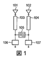
- FIG. 1 is a circuit diagram of an antenna device according to a first embodiment of the present invention.
- FIG. 2 is a circuit diagram in which a matching circuit is added to the antenna end portion of the first embodiment of FIG.
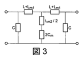
- FIG. 3 is a circuit diagram showing an example of a low-pass filter that can be applied to the first embodiment of the present invention.
- FIG. 4 is a diagram illustrating an antenna device that embodies the first embodiment of the present invention.
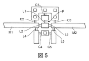
- FIG. 5 is a diagram illustrating details of the filter circuit and the matching circuit in FIG.
- FIG. 6 is a diagram illustrating frequency characteristics of S parameters of the antenna device of FIG.
- FIG. 7 is a diagram showing the frequency characteristics of the correlation coefficient of the antenna apparatus of FIG.
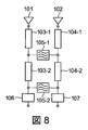
- FIG. 8 is a circuit diagram of an antenna device according to the second embodiment of the present invention.
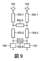
- FIG. 9 is a circuit diagram showing an antenna apparatus according to the third embodiment of the present invention.
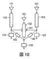
- FIG. 10 is a circuit diagram showing an antenna apparatus according to the fourth embodiment of the present invention.
- FIG. 1 is a circuit diagram showing a basic structure of an antenna device according to a first embodiment of the present invention.
- 101 and 102 are first and second antenna elements
- 103 and 104 are first and second transmission lines
- 105 is a filter circuit
- 106 and 107 are first and second matching circuits.
- the first matching circuit 106 and the second matching circuit 107 perform impedance matching when looking into the first antenna element 101 and the second antenna element 102 side.
- the first antenna element 101 and the second antenna element 102 may have different structures, different types, and different arrangements.
- the first transmission line 103 and the second transmission line 104 may have any type, length, and shape as long as the condition of the expression (1) described below is satisfied.
- the filter circuit 105 for example, a low-pass filter, a high-pass filter, a band filter, and a band elimination filter can be used, and a filter using a lumped constant circuit or a distributed constant circuit can be used.
- the filter circuit 105 in FIG. 1 or FIG. 2 can be constituted by a low-pass filter circuit combining an inductor (L + L m1 ), L m2 / 2, and capacitors C and 2C m as shown in FIG.
- FIG. 4 is a diagram showing an antenna device that specifically implements the first embodiment of the present invention with a substrate.
- an inverted F antenna is used as an antenna element, and microstrip lines M1 and M2 are wired from antenna elements A1 and A2 on both sides of the substrate, respectively, and connected to a filter circuit F and a matching circuit in the center of the substrate.
- the matching circuit 101-2 and the matching circuit 102-2 in FIG. 2 correspond to a short line in the inverted F antenna.
- FIG. 5 is a diagram illustrating details of the filter circuit F and the matching circuit in the antenna device of FIG. L1 to L3 and C1 to C3 are lumped constants constituting the filter circuit F, and L4, L5, C4, and C5 represent lumped constants constituting the matching circuit.
- L1 to L3 are inductances of inductors constituting a low-pass filter
- L4 and L5 are inductances of inductors constituting a matching circuit
- C1 to C3 are capacitances of capacitors constituting a low-pass filter
- C4 and C5 are It is a capacitance of a capacitor constituting the matching circuit.
- L1 3.8 nH
- L2 4.5 nH
- L3 4.5 nH
- L4 1 nH
- L5 1 nH
- C1 2.7 pF
- C2 2.05 pF
- C3 2.05 pF
- C4 2 pF
- C5 2 pF.
- the filter circuit F is designed to have a pass band in the 850 MHz band and a stop band in the 2.1 GHz band.
- the electrical length ⁇ 1 of the microstrip line M1 which is the first transmission line, and the second so as to satisfy the following conditional expression (1) in a desired plurality of frequency bands:
- the electrical length ⁇ 2 of the microstrip line M2, which is the transmission line, and the lumped constant value of the filter circuit F are designed.
- B represents the susceptance of the filter circuit F
- ⁇ and ⁇ represent the coupling coefficient and the phase difference between the antenna elements A1 and A2 when only the antenna elements A1 and A2 are mounted, respectively.
- Y 0 is characteristic admittance.
- the sum of the phase difference between the antenna elements A1 and A2 and the electrical length of the microstrip lines M1 and M2 is ⁇ 90 ° ( ⁇ / 2), and the susceptance of the filter circuit F is a coupling coefficient ⁇ between the antenna elements A1 and A2.
- the mutual coupling between the antenna elements A1 and A2 can be suppressed by designing in a desired plurality of frequency bands so that the determined non-coupling value B is obtained.
- the fact that the susceptance of the filter circuit F becomes the non-coupling value B in the above equation (1) indicates a situation where the S parameter S21 (or S12) described later is minimized. Therefore, the condition of the above formula (1) can be searched using the lumped constant in the filter circuit F as a parameter.
- FIG. 6 is a diagram illustrating the frequency characteristics of the S parameter of the substrate of FIG.
- S parameters are shown when the power feeding part P1 and the power feeding part P2 shown in FIG. 4 are antenna ports.
- FIG. 7 shows the correlation coefficient between ports calculated from the S parameter of FIG.
- the correlation coefficient ⁇ e can be expressed by the following equation (2) when the two antenna structures have a symmetrical structure. It can be seen that the correlation coefficient ⁇ e is almost zero at 850 MHz and 2.1 GHz, and sufficiently satisfies the low correlation necessary for obtaining good quality characteristics in MIMO communication. [Other Embodiments]
- the isolation can be realized even in a plurality of bands by mounting the filter circuits in multiple stages.
- FIG. 8 A configuration for this purpose is shown in FIG. 8 as a second embodiment.
- this antenna apparatus has a filter circuit 105-1 connected between a transmission line 103-1 connected to the antenna element 101 and a transmission line 104-1 connected to the antenna element 102, and a transmission line 103-1.
- the filter circuit 105-2 is connected between the transmission line 103-2 connected to the transmission line 104-2 and the transmission line 104-2 connected to the transmission line 104-1.
- 106 and 107 are matching circuits.
- two stages of filter circuits 105-1 and 105-2 are inserted between the transmission lines, but there is no problem even if they are mounted more than that. Inserting filter circuits in multiple stages facilitates isolation between ports in a plurality of bands.
- the present invention can be used by combining a filter circuit 105-4 and a susceptance element 105-3 including an inductor or a capacitor for isolation between ports. It becomes possible to cope with the bandwidth of.
- FIG. 9 the present invention can be used by combining a filter circuit 105-4 and a susceptance element 105-3 including an inductor or a capacitor for isolation between ports. It becomes possible to cope with the bandwidth of.
- FIG. 9 the present invention can be used by combining a filter circuit 105-4 and a susceptance element 105-3 including an inductor or a capacitor
- the antenna device connects a susceptance element 105-3 between a transmission line 103-1 connected to the antenna element 101 and a transmission line 104-1 connected to the antenna element 102.
- the filter circuit 105-4 is connected between the transmission line 103-2 connected to the transmission line 103-1, and the transmission line 104-2 connected to the transmission line 104-1.
- the configuration using one filter circuit and one susceptance element is shown as a specific example, but these may be inserted in multiple stages.
- 106 and 107 are matching circuits.
- the present invention is further applicable to the case where there are three or more antenna elements.
- a configuration for this purpose is shown in FIG. 10 as a fourth embodiment. In FIG.
- transmission lines 112, 122, and 132 are connected to antenna elements 111, 121, and 131, respectively, and between the transmission line 112 and the transmission line 122, a filter circuit 141, and between the transmission line 122 and the transmission line 132.
- a filter circuit 143 is connected between the filter circuit 142, the transmission line 112, and the transmission line 132, respectively.
- a matching circuit 113 is connected to the end of the transmission line 112, a matching circuit 123 is connected to the end of the transmission line 122, and a matching circuit 133 is connected to the end of the transmission line 132.
- the present invention can be similarly applied to a case where the number of antenna elements is larger.
- the present invention is applicable to a wireless communication device using a plurality of antenna elements.
- a wireless communication device using a plurality of antenna elements.
- it can be installed in a mobile communication base station and terminal, or a device such as a wireless LAN (Local Area Network) router.
- LAN Local Area Network
Landscapes
- Details Of Aerials (AREA)
- Variable-Direction Aerials And Aerial Arrays (AREA)
- Transceivers (AREA)
Description
そのための解決策として、例えば特許文献1の図10Bに記載されているアンテナ構造物では、隣接するアンテナ素子間に連結素子を設け、連結素子の長さや設置箇所を調整することで適切なサセプタンス値を与え、アンテナポート間のアイソレーションを抑制することができる構造を採用している。
本発明は、互いに共通の複数周波数帯を有する、複数のアンテナ素子に対し、各周波数帯においてアンテナポート間のアイソレーションを補償するアンテナ装置を提供しようとするものである。
図2は、図1の第1の実施形態のアンテナ端部に整合回路を追加した回路図である。
図3は、本発明の第1の実施形態に適用され得る低域フィルタの一例を表した回路図である。
図4は、本発明の第1の実施形態を具現化したアンテナ装置を表す図である。
図5は、図4におけるフィルタ回路および整合回路の詳細を説明した図である。
図6は、図4のアンテナ装置のSパラメータの周波数特性を示す図である。
図7は、図4のアンテナ装置の相関係数の周波数特性を示す図である。
図8は、本発明の第2の実施形態によるアンテナ装置の回路図である。
図9は、本発明の第3の実施形態によるアンテナ装置を示す回路図である。
図10は、本発明の第4の実施形態によるアンテナ装置を示す回路図である。
本発明に係るアンテナ装置の第1の実施形態について図面を参照して詳細に説明する。
図1は本発明の第1の実施形態によるアンテナ装置の基本構造を表す回路図である。
図1において、101,102は第1,第2のアンテナ素子、103,104は第1,第2の伝送線路、105はフィルタ回路、106,107は第1,第2の整合回路である。第1の整合回路106,第2の整合回路107は、第1のアンテナ素子101,第2のアンテナ素子102側を覗いた際のインピーダンス整合を行う。
第1のアンテナ素子101と第2のアンテナ素子102は同じ周波数帯を有する限りにおいて、異なる構造、異なる種類、異なる配置をとっていても良い。
第1の伝送線路103と第2の伝送線路104は、以後に説明する式(1)の条件を満たす限りにおいてはどのような種類、長さ、形状をとっていても良い。
フィルタ回路105は、例えば低域フィルタ、高域フィルタ、帯域フィルタ、帯域除去フィルタを用いることができ、集中定数回路や分布定数回路を用いたフィルタを用いることができる。回路105においてフィルタ回路を用いることで、アンテナポート間アイソレーションを実現する上で重要な非結合値を決定する上でのサセプタンスの周波数特性に複雑な変化を与えることができ、マルチバンドでのアンテナポート間アイソレーションを容易にする。
図2は図1で表すアンテナ装置に対し、アンテナ素子101−1、102−1付近にそれぞれ整合回路101−2、102−2を付加したアンテナ装置の回路図である。
図2における整合回路101−2と整合回路102−2は設計において必ずしも必要ではないが、アンテナ装置の設計を簡単にするために実装することができるのでここでは便宜的に導入する。
図1あるいは図2におけるフィルタ回路105は、例えば図3のようなインダクタ(L+Lm1),Lm2/2およびキャパシタC,2Cmを組み合わせた低域フィルタ回路で構成できる。Lは低域フィルタを構成するインダクタのインダクタンス、C,Cmは低域フィルタを構成するキャパシタのキャパシタンス、Lm1,Lm2は低域フィルタを構成するインダクタのインダクタンスである。
図4は本発明の第1の実施形態を具体的に基板で実現したアンテナ装置を表す図である。ここではアンテナ素子として逆Fアンテナを用い、基板両側のアンテナ素子A1,A2からそれぞれマイクロストリップ線路M1,M2が配線され、基板の中央にあるフィルタ回路F及び整合回路へと接続される。図2における整合回路101−2と整合回路102−2は逆Fアンテナにおけるショートラインに相当する。2本のアンテナ素子A1,A2は共に850MHz帯および2.1GHz帯で周波数帯を持つように設計されている。
図5は図4のアンテナ装置におけるフィルタ回路Fおよび整合回路の詳細を説明した図である。L1~L3およびC1~C3まではフィルタ回路Fを構成する集中定数であり、L4、L5、C4、C5は整合回路を構成する集中定数を表す。具体的には、L1~L3は低域フィルタを構成するインダクタのインダクタンス、L4,L5は整合回路を構成するインダクタのインダクタンス、C1~C3は低域フィルタを構成するキャパシタのキャパシタンス、C4,C5は整合回路を構成するキャパシタのキャパシタンスである。ここでは、L1=3.8nH,L2=4.5nH,L3=4.5nH,L4=1nH,L5=1nH,C1=2.7pF,C2=2.05pF,C3=2.05pF,C4=2pF,C5=2pFである。
フィルタ回路Fは850MHz帯においてパスバンド、2.1GHz帯でストップバンドを持つように設計されている。
アンテナポート間のアイソレーションを実現するためには、所望の複数の周波数帯において以下の条件式(1)を満たすように、第1の伝送線路であるマイクロストリップ線路M1の電気長θ1、第2の伝送線路であるマイクロストリップ線路M2の電気長θ2およびフィルタ回路Fの集中定数値を設計する。

図6は、図4の基板のSパラメータの周波数特性を表す図である。ここでは、図4に示した給電部P1と給電部P2をアンテナポートとした際のSパラメータを表している。ここではS11とS21のみを示したが、S22とS12もそれぞれS11とS21と同様の結果を示す。これは、アンテナ基板の対称性・可逆性からS22=S11,S12=S21が保障されるからである。アンテナの周波数帯である850MHzおよび2.1GHzにおいてS11とS21は共にディップを示していることから、両帯域において、アンテナの共振特性とともにアンテナポート間のアイソレーションが取れていることが分かる。
図7は図6のSパラメータから計算されたポート間の相関係数である。相関係数ρeは2本のアンテナ構造が対称的な構造を持つ場合には以下のような式(2)で表すことができる。

[他の実施形態]
上記第1の実施形態において、フィルタ回路を多段に実装することでより複数の帯域においてもアイソレーションが実現可能となる。
そのための構成を、第2の実施形態として図8に示す。
図8において、このアンテナ装置は、アンテナ素子101に接続した伝送線路103−1とアンテナ素子102に接続した伝送線路104−1の間にフィルタ回路105−1を接続すると共に、伝送線路103−1に接続した伝送線路103−2と伝送線路104−1に接続した伝送線路104−2の間にフィルタ回路105−2を接続した多段構成としている。106,107は整合回路である。第2の実施形態では、具体例として伝送線路間に2段のフィルタ回路105−1,105−2を挿入しているが、それ以上に実装しても問題ない。フィルタ回路を多段に挿入することで、複数の帯域におけるポート間アイソレーションが容易となる。
本発明は更に、第3の実施形態として図9に示すように、ポート間のアイソレーションのためにフィルタ回路105−4と、インダクタあるいはキャパシタからなるサセプタンス素子105−3を組み合わせて用いることでも複数の帯域に対応が可能となる。
図9において、第3の実施形態によるアンテナ装置は、アンテナ素子101に接続した伝送線路103−1とアンテナ素子102に接続した伝送線路104−1の間にサセプタンス素子105−3を接続すると共に、伝送線路103−1に接続した伝送線路103−2と伝送線路104−1に接続した伝送線路104−2の間にフィルタ回路105−4を接続した構成としている。第3の実施形態では、具体例としてフィルタ回路とサセプタンス素子をそれぞれ一つずつ用いた構成を示したが、これらを多段に挿入してもよい。106、107は整合回路である。
本発明は更に、アンテナ素子が3本以上の場合にも適用が可能である。そのための構成を第4の実施形態として図10に示す。
図10において、アンテナ素子111,121,131にそれぞれ伝送線路112,122,132が接続され、伝送線路112と伝送線路122の間にはフィルタ回路141、伝送線路122と伝送線路132の間にはフィルタ回路142、伝送線路112と伝送線路132の間にはフィルタ回路143がそれぞれ接続されている。伝送線路112の端部には整合回路113、伝送線路122の端部には整合回路123、伝送線路132の端部には整合回路133がそれぞれ接続されている。ここでは簡単のためにアンテナ素子が3本の場合を示しているが、それ以上の本数の場合にも同様にして適用可能である。
以上、本発明を、複数の実施形態を参照して説明したが、本発明は上記実施形態に限定されるものではない。本発明の構成や詳細には、請求項に記載された本発明の精神や範囲内で当業者が理解し得る様々な変更をすることができる。
この出願は、2012年9月13日に出願された日本出願特願2012−201884を基礎とする優先権を主張し、その開示のすべてをここに取り込む。
103,104,103−1、103−2,104−1,104−2,112,122,132 伝送線路
101−2,102−2,106,107,113,123,133 整合回路
105,105−1,105−2,105−4,141,142,143 フィルタ回路
105−3 サセプタンス素子
Claims (5)
- 少なくとも2本以上の複数のアンテナ素子と、
前記各アンテナ素子にそれぞれ接続される伝送線路と、
前記各伝送線路の間に接続されるフィルタ回路と、
前記各伝送線路の終端部に接続される整合回路と、を含み、
前記各アンテナ素子は互いに共通の複数周波数帯を有し、
前記フィルタ回路は前記アンテナ素子の特定の周波数帯で通過域を有し、
前記フィルタ回路は集中定数回路あるいは分布定数回路を用いて構成され、
前記フィルタ回路は前記各アンテナ素子間の相互結合を、
複数の周波数帯にわたって抑制することを特徴とするアンテナ装置。 - 複数の周波数にわたって、前記アンテナ素子間の位相差と前記伝送線路の電気長の合計を±90°とし、かつ前記フィルタ回路のサセプタンスがアンテナ間の結合係数で決まる非結合値を与えることで、アンテナ間の相互結合を抑制することを特徴とする請求項1に記載のアンテナ装置。
- 前記フィルタ回路を伝送線路間に複数挿入することで、複数の周波数帯でアンテナ素子間の相互結合を抑制することを特徴とする請求項1または2に記載のアンテナ装置。
- 前記フィルタ回路と共にサセプタンス素子を1段以上挿入することで複数の周波数帯でアンテナ素子間の相互結合を抑制することを特徴とする請求項1または2に記載のアンテナ装置。
- 前記整合回路はアンテナ素子側のインピーダンスを整合することを特徴とする請求項1~4のいずれかに記載のアンテナ装置。
Priority Applications (2)
| Application Number | Priority Date | Filing Date | Title |
|---|---|---|---|
| JP2014535419A JP6197793B2 (ja) | 2012-09-13 | 2013-07-19 | アンテナ装置 |
| US14/424,813 US20150255863A1 (en) | 2012-09-13 | 2013-07-19 | Antenna device |
Applications Claiming Priority (2)
| Application Number | Priority Date | Filing Date | Title |
|---|---|---|---|
| JP2012201884 | 2012-09-13 | ||
| JP2012-201884 | 2012-09-13 |
Publications (1)
| Publication Number | Publication Date |
|---|---|
| WO2014041903A1 true WO2014041903A1 (ja) | 2014-03-20 |
Family
ID=50278032
Family Applications (1)
| Application Number | Title | Priority Date | Filing Date |
|---|---|---|---|
| PCT/JP2013/070261 Ceased WO2014041903A1 (ja) | 2012-09-13 | 2013-07-19 | アンテナ装置 |
Country Status (3)
| Country | Link |
|---|---|
| US (1) | US20150255863A1 (ja) |
| JP (1) | JP6197793B2 (ja) |
| WO (1) | WO2014041903A1 (ja) |
Cited By (3)
| Publication number | Priority date | Publication date | Assignee | Title |
|---|---|---|---|---|
| CN106571526A (zh) * | 2016-04-06 | 2017-04-19 | 昆山睿翔讯通通信技术有限公司 | 移动通讯系统终端mimo天线的解耦方法及解耦网络 |
| WO2020178897A1 (ja) * | 2019-03-01 | 2020-09-10 | 三菱電機株式会社 | アンテナ装置 |
| WO2020207425A1 (zh) * | 2019-04-10 | 2020-10-15 | 上海众链科技有限公司 | 多天线系统及移动终端 |
Families Citing this family (5)
| Publication number | Priority date | Publication date | Assignee | Title |
|---|---|---|---|---|
| US9543644B2 (en) * | 2014-07-01 | 2017-01-10 | The Chinese University Of Hong Kong | Method and an apparatus for decoupling multiple antennas in a compact antenna array |
| US11251522B2 (en) | 2019-08-15 | 2022-02-15 | Ademco Inc. | Cancelation circuit for radio frequency antenna systems |
| WO2021227827A1 (zh) * | 2020-05-12 | 2021-11-18 | 西安电子科技大学 | 天线装置和电子设备 |
| WO2022201414A1 (ja) * | 2021-03-25 | 2022-09-29 | 三菱電機株式会社 | 減結合回路 |
| CN117397121A (zh) * | 2021-08-18 | 2024-01-12 | 华为技术有限公司 | 一种天线阵列、天线系统及通信设备 |
Citations (3)
| Publication number | Priority date | Publication date | Assignee | Title |
|---|---|---|---|---|
| JP2009521898A (ja) * | 2007-04-20 | 2009-06-04 | スカイクロス,アイエヌシー. | マルチモードアンテナ構造物 |
| WO2010061541A1 (ja) * | 2008-11-25 | 2010-06-03 | パナソニック株式会社 | アレーアンテナ装置及び無線通信装置 |
| JP2011182281A (ja) * | 2010-03-03 | 2011-09-15 | Panasonic Corp | アンテナ装置及びこれを搭載した携帯無線端末 |
Family Cites Families (2)
| Publication number | Priority date | Publication date | Assignee | Title |
|---|---|---|---|---|
| US7629930B2 (en) * | 2006-10-20 | 2009-12-08 | Hong Kong Applied Science And Technology Research Institute Co., Ltd. | Systems and methods using ground plane filters for device isolation |
| KR100895448B1 (ko) * | 2007-07-03 | 2009-05-07 | 삼성전자주식회사 | 소형화된 mimo 안테나 |
-
2013
- 2013-07-19 JP JP2014535419A patent/JP6197793B2/ja active Active
- 2013-07-19 WO PCT/JP2013/070261 patent/WO2014041903A1/ja not_active Ceased
- 2013-07-19 US US14/424,813 patent/US20150255863A1/en not_active Abandoned
Patent Citations (3)
| Publication number | Priority date | Publication date | Assignee | Title |
|---|---|---|---|---|
| JP2009521898A (ja) * | 2007-04-20 | 2009-06-04 | スカイクロス,アイエヌシー. | マルチモードアンテナ構造物 |
| WO2010061541A1 (ja) * | 2008-11-25 | 2010-06-03 | パナソニック株式会社 | アレーアンテナ装置及び無線通信装置 |
| JP2011182281A (ja) * | 2010-03-03 | 2011-09-15 | Panasonic Corp | アンテナ装置及びこれを搭載した携帯無線端末 |
Cited By (4)
| Publication number | Priority date | Publication date | Assignee | Title |
|---|---|---|---|---|
| CN106571526A (zh) * | 2016-04-06 | 2017-04-19 | 昆山睿翔讯通通信技术有限公司 | 移动通讯系统终端mimo天线的解耦方法及解耦网络 |
| WO2020178897A1 (ja) * | 2019-03-01 | 2020-09-10 | 三菱電機株式会社 | アンテナ装置 |
| JPWO2020178897A1 (ja) * | 2019-03-01 | 2021-06-10 | 三菱電機株式会社 | アンテナ装置 |
| WO2020207425A1 (zh) * | 2019-04-10 | 2020-10-15 | 上海众链科技有限公司 | 多天线系统及移动终端 |
Also Published As
| Publication number | Publication date |
|---|---|
| JPWO2014041903A1 (ja) | 2016-08-18 |
| JP6197793B2 (ja) | 2017-09-20 |
| US20150255863A1 (en) | 2015-09-10 |
Similar Documents
| Publication | Publication Date | Title |
|---|---|---|
| JP6197793B2 (ja) | アンテナ装置 | |
| JP6032515B2 (ja) | アンテナ及び端末 | |
| US9543644B2 (en) | Method and an apparatus for decoupling multiple antennas in a compact antenna array | |
| US20130057438A1 (en) | Antenna device and portable wireless terminal equipped with the same | |
| JP5424500B2 (ja) | アンテナ装置及びこれを搭載した携帯無線端末 | |
| TWI521788B (zh) | 天線組合及無線通訊裝置 | |
| CN113287230A (zh) | 天线装置及终端 | |
| US10374306B2 (en) | MIMO antenna having adjustable decoupling structure | |
| US20130057448A1 (en) | Antenna device and portable wireless terminal equipped with the same | |
| JP2014112824A (ja) | アンテナ装置 | |
| CN105960737A (zh) | 一种多频通信天线以及基站 | |
| WO2010114570A1 (en) | Radio frequency power divider and combiner circuit | |
| US8115569B2 (en) | Monoblock dielectric multiplexer capable of processing multi-band signals | |
| US9379455B2 (en) | Antenna circuit using multiple independent antennas simultaneously through a single feed | |
| CN107112630B (zh) | 具有隔离调整部的mimo天线 | |
| CN104466401A (zh) | 多天线终端 | |
| JP5804076B2 (ja) | Lcフィルタ回路及び高周波モジュール | |
| CN105322295A (zh) | 用于移动终端的多频天线及其电子设备 | |
| CN113131194B (zh) | 一种阵列天线及通信设备 | |
| JP7150201B1 (ja) | 減結合回路 | |
| US8542080B2 (en) | All-pass network | |
| US20150126131A1 (en) | Wireless communication device and measuring device therefor | |
| CN106450667B (zh) | 一种零阶谐振天线和无线路由器 | |
| KR101672035B1 (ko) | 안테나 대역폭 확장장치 | |
| JP2018186372A (ja) | インピーダンス変成回路 |
Legal Events
| Date | Code | Title | Description |
|---|---|---|---|
| 121 | Ep: the epo has been informed by wipo that ep was designated in this application |
Ref document number: 13836432 Country of ref document: EP Kind code of ref document: A1 |
|
| ENP | Entry into the national phase |
Ref document number: 2014535419 Country of ref document: JP Kind code of ref document: A |
|
| WWE | Wipo information: entry into national phase |
Ref document number: 14424813 Country of ref document: US |
|
| NENP | Non-entry into the national phase |
Ref country code: DE |
|
| 122 | Ep: pct application non-entry in european phase |
Ref document number: 13836432 Country of ref document: EP Kind code of ref document: A1 |