WO2014041866A1 - センサ、表示装置、制御プログラムおよび記録媒体 - Google Patents
センサ、表示装置、制御プログラムおよび記録媒体 Download PDFInfo
- Publication number
- WO2014041866A1 WO2014041866A1 PCT/JP2013/067385 JP2013067385W WO2014041866A1 WO 2014041866 A1 WO2014041866 A1 WO 2014041866A1 JP 2013067385 W JP2013067385 W JP 2013067385W WO 2014041866 A1 WO2014041866 A1 WO 2014041866A1
- Authority
- WO
- WIPO (PCT)
- Prior art keywords
- infrared
- specific color
- light receiving
- receiving element
- color
- Prior art date
- Legal status (The legal status is an assumption and is not a legal conclusion. Google has not performed a legal analysis and makes no representation as to the accuracy of the status listed.)
- Ceased
Links
Images





Classifications
-
- G—PHYSICS
- G01—MEASURING; TESTING
- G01J—MEASUREMENT OF INTENSITY, VELOCITY, SPECTRAL CONTENT, POLARISATION, PHASE OR PULSE CHARACTERISTICS OF INFRARED, VISIBLE OR ULTRAVIOLET LIGHT; COLORIMETRY; RADIATION PYROMETRY
- G01J3/00—Spectrometry; Spectrophotometry; Monochromators; Measuring colours
- G01J3/46—Measurement of colour; Colour measuring devices, e.g. colorimeters
- G01J3/50—Measurement of colour; Colour measuring devices, e.g. colorimeters using electric radiation detectors
- G01J3/51—Measurement of colour; Colour measuring devices, e.g. colorimeters using electric radiation detectors using colour filters
-
- G—PHYSICS
- G09—EDUCATION; CRYPTOGRAPHY; DISPLAY; ADVERTISING; SEALS
- G09G—ARRANGEMENTS OR CIRCUITS FOR CONTROL OF INDICATING DEVICES USING STATIC MEANS TO PRESENT VARIABLE INFORMATION
- G09G3/00—Control arrangements or circuits, of interest only in connection with visual indicators other than cathode-ray tubes
- G09G3/20—Control arrangements or circuits, of interest only in connection with visual indicators other than cathode-ray tubes for presentation of an assembly of a number of characters, e.g. a page, by composing the assembly by combination of individual elements arranged in a matrix no fixed position being assigned to or needed to be assigned to the individual characters or partial characters
- G09G3/34—Control arrangements or circuits, of interest only in connection with visual indicators other than cathode-ray tubes for presentation of an assembly of a number of characters, e.g. a page, by composing the assembly by combination of individual elements arranged in a matrix no fixed position being assigned to or needed to be assigned to the individual characters or partial characters by control of light from an independent source
- G09G3/3406—Control of illumination source
-
- G—PHYSICS
- G01—MEASURING; TESTING
- G01J—MEASUREMENT OF INTENSITY, VELOCITY, SPECTRAL CONTENT, POLARISATION, PHASE OR PULSE CHARACTERISTICS OF INFRARED, VISIBLE OR ULTRAVIOLET LIGHT; COLORIMETRY; RADIATION PYROMETRY
- G01J1/00—Photometry, e.g. photographic exposure meter
- G01J1/10—Photometry, e.g. photographic exposure meter by comparison with reference light or electric value provisionally void
- G01J1/20—Photometry, e.g. photographic exposure meter by comparison with reference light or electric value provisionally void intensity of the measured or reference value being varied to equalise their effects at the detectors, e.g. by varying incidence angle
- G01J1/28—Photometry, e.g. photographic exposure meter by comparison with reference light or electric value provisionally void intensity of the measured or reference value being varied to equalise their effects at the detectors, e.g. by varying incidence angle using variation of intensity or distance of source
- G01J1/30—Photometry, e.g. photographic exposure meter by comparison with reference light or electric value provisionally void intensity of the measured or reference value being varied to equalise their effects at the detectors, e.g. by varying incidence angle using variation of intensity or distance of source using electric radiation detectors
- G01J1/32—Photometry, e.g. photographic exposure meter by comparison with reference light or electric value provisionally void intensity of the measured or reference value being varied to equalise their effects at the detectors, e.g. by varying incidence angle using variation of intensity or distance of source using electric radiation detectors adapted for automatic variation of the measured or reference value
-
- G—PHYSICS
- G01—MEASURING; TESTING
- G01J—MEASUREMENT OF INTENSITY, VELOCITY, SPECTRAL CONTENT, POLARISATION, PHASE OR PULSE CHARACTERISTICS OF INFRARED, VISIBLE OR ULTRAVIOLET LIGHT; COLORIMETRY; RADIATION PYROMETRY
- G01J3/00—Spectrometry; Spectrophotometry; Monochromators; Measuring colours
- G01J3/46—Measurement of colour; Colour measuring devices, e.g. colorimeters
- G01J3/50—Measurement of colour; Colour measuring devices, e.g. colorimeters using electric radiation detectors
- G01J3/506—Measurement of colour; Colour measuring devices, e.g. colorimeters using electric radiation detectors measuring the colour produced by screens, monitors, displays or CRTs
-
- G—PHYSICS
- G02—OPTICS
- G02F—OPTICAL DEVICES OR ARRANGEMENTS FOR THE CONTROL OF LIGHT BY MODIFICATION OF THE OPTICAL PROPERTIES OF THE MEDIA OF THE ELEMENTS INVOLVED THEREIN; NON-LINEAR OPTICS; FREQUENCY-CHANGING OF LIGHT; OPTICAL LOGIC ELEMENTS; OPTICAL ANALOGUE/DIGITAL CONVERTERS
- G02F1/00—Devices or arrangements for the control of the intensity, colour, phase, polarisation or direction of light arriving from an independent light source, e.g. switching, gating or modulating; Non-linear optics
- G02F1/01—Devices or arrangements for the control of the intensity, colour, phase, polarisation or direction of light arriving from an independent light source, e.g. switching, gating or modulating; Non-linear optics for the control of the intensity, phase, polarisation or colour
- G02F1/13—Devices or arrangements for the control of the intensity, colour, phase, polarisation or direction of light arriving from an independent light source, e.g. switching, gating or modulating; Non-linear optics for the control of the intensity, phase, polarisation or colour based on liquid crystals, e.g. single liquid crystal display cells
- G02F1/133—Constructional arrangements; Operation of liquid crystal cells; Circuit arrangements
- G02F1/1333—Constructional arrangements; Manufacturing methods
- G02F1/1335—Structural association of cells with optical devices, e.g. polarisers or reflectors
- G02F1/1336—Illuminating devices
- G02F1/133602—Direct backlight
- G02F1/133603—Direct backlight with LEDs
-
- G—PHYSICS
- G09—EDUCATION; CRYPTOGRAPHY; DISPLAY; ADVERTISING; SEALS
- G09G—ARRANGEMENTS OR CIRCUITS FOR CONTROL OF INDICATING DEVICES USING STATIC MEANS TO PRESENT VARIABLE INFORMATION
- G09G3/00—Control arrangements or circuits, of interest only in connection with visual indicators other than cathode-ray tubes
- G09G3/20—Control arrangements or circuits, of interest only in connection with visual indicators other than cathode-ray tubes for presentation of an assembly of a number of characters, e.g. a page, by composing the assembly by combination of individual elements arranged in a matrix no fixed position being assigned to or needed to be assigned to the individual characters or partial characters
- G09G3/34—Control arrangements or circuits, of interest only in connection with visual indicators other than cathode-ray tubes for presentation of an assembly of a number of characters, e.g. a page, by composing the assembly by combination of individual elements arranged in a matrix no fixed position being assigned to or needed to be assigned to the individual characters or partial characters by control of light from an independent source
- G09G3/3406—Control of illumination source
- G09G3/3413—Details of control of colour illumination sources
-
- G—PHYSICS
- G09—EDUCATION; CRYPTOGRAPHY; DISPLAY; ADVERTISING; SEALS
- G09G—ARRANGEMENTS OR CIRCUITS FOR CONTROL OF INDICATING DEVICES USING STATIC MEANS TO PRESENT VARIABLE INFORMATION
- G09G3/00—Control arrangements or circuits, of interest only in connection with visual indicators other than cathode-ray tubes
- G09G3/20—Control arrangements or circuits, of interest only in connection with visual indicators other than cathode-ray tubes for presentation of an assembly of a number of characters, e.g. a page, by composing the assembly by combination of individual elements arranged in a matrix no fixed position being assigned to or needed to be assigned to the individual characters or partial characters
- G09G3/34—Control arrangements or circuits, of interest only in connection with visual indicators other than cathode-ray tubes for presentation of an assembly of a number of characters, e.g. a page, by composing the assembly by combination of individual elements arranged in a matrix no fixed position being assigned to or needed to be assigned to the individual characters or partial characters by control of light from an independent source
- G09G3/36—Control arrangements or circuits, of interest only in connection with visual indicators other than cathode-ray tubes for presentation of an assembly of a number of characters, e.g. a page, by composing the assembly by combination of individual elements arranged in a matrix no fixed position being assigned to or needed to be assigned to the individual characters or partial characters by control of light from an independent source using liquid crystals
-
- G—PHYSICS
- G09—EDUCATION; CRYPTOGRAPHY; DISPLAY; ADVERTISING; SEALS
- G09G—ARRANGEMENTS OR CIRCUITS FOR CONTROL OF INDICATING DEVICES USING STATIC MEANS TO PRESENT VARIABLE INFORMATION
- G09G5/00—Control arrangements or circuits for visual indicators common to cathode-ray tube indicators and other visual indicators
- G09G5/02—Control arrangements or circuits for visual indicators common to cathode-ray tube indicators and other visual indicators characterised by the way in which colour is displayed
- G09G5/026—Control of mixing and/or overlay of colours in general
-
- G—PHYSICS
- G02—OPTICS
- G02F—OPTICAL DEVICES OR ARRANGEMENTS FOR THE CONTROL OF LIGHT BY MODIFICATION OF THE OPTICAL PROPERTIES OF THE MEDIA OF THE ELEMENTS INVOLVED THEREIN; NON-LINEAR OPTICS; FREQUENCY-CHANGING OF LIGHT; OPTICAL LOGIC ELEMENTS; OPTICAL ANALOGUE/DIGITAL CONVERTERS
- G02F1/00—Devices or arrangements for the control of the intensity, colour, phase, polarisation or direction of light arriving from an independent light source, e.g. switching, gating or modulating; Non-linear optics
- G02F1/01—Devices or arrangements for the control of the intensity, colour, phase, polarisation or direction of light arriving from an independent light source, e.g. switching, gating or modulating; Non-linear optics for the control of the intensity, phase, polarisation or colour
- G02F1/13—Devices or arrangements for the control of the intensity, colour, phase, polarisation or direction of light arriving from an independent light source, e.g. switching, gating or modulating; Non-linear optics for the control of the intensity, phase, polarisation or colour based on liquid crystals, e.g. single liquid crystal display cells
- G02F1/133—Constructional arrangements; Operation of liquid crystal cells; Circuit arrangements
- G02F1/1333—Constructional arrangements; Manufacturing methods
- G02F1/1335—Structural association of cells with optical devices, e.g. polarisers or reflectors
- G02F1/1336—Illuminating devices
- G02F1/133621—Illuminating devices providing coloured light
-
- G—PHYSICS
- G02—OPTICS
- G02F—OPTICAL DEVICES OR ARRANGEMENTS FOR THE CONTROL OF LIGHT BY MODIFICATION OF THE OPTICAL PROPERTIES OF THE MEDIA OF THE ELEMENTS INVOLVED THEREIN; NON-LINEAR OPTICS; FREQUENCY-CHANGING OF LIGHT; OPTICAL LOGIC ELEMENTS; OPTICAL ANALOGUE/DIGITAL CONVERTERS
- G02F2201/00—Constructional arrangements not provided for in groups G02F1/00 - G02F7/00
- G02F2201/58—Arrangements comprising a monitoring photodetector
-
- G—PHYSICS
- G09—EDUCATION; CRYPTOGRAPHY; DISPLAY; ADVERTISING; SEALS
- G09G—ARRANGEMENTS OR CIRCUITS FOR CONTROL OF INDICATING DEVICES USING STATIC MEANS TO PRESENT VARIABLE INFORMATION
- G09G2320/00—Control of display operating conditions
- G09G2320/02—Improving the quality of display appearance
- G09G2320/0242—Compensation of deficiencies in the appearance of colours
-
- G—PHYSICS
- G09—EDUCATION; CRYPTOGRAPHY; DISPLAY; ADVERTISING; SEALS
- G09G—ARRANGEMENTS OR CIRCUITS FOR CONTROL OF INDICATING DEVICES USING STATIC MEANS TO PRESENT VARIABLE INFORMATION
- G09G2320/00—Control of display operating conditions
- G09G2320/02—Improving the quality of display appearance
- G09G2320/0285—Improving the quality of display appearance using tables for spatial correction of display data
-
- G—PHYSICS
- G09—EDUCATION; CRYPTOGRAPHY; DISPLAY; ADVERTISING; SEALS
- G09G—ARRANGEMENTS OR CIRCUITS FOR CONTROL OF INDICATING DEVICES USING STATIC MEANS TO PRESENT VARIABLE INFORMATION
- G09G2320/00—Control of display operating conditions
- G09G2320/06—Adjustment of display parameters
- G09G2320/0626—Adjustment of display parameters for control of overall brightness
-
- G—PHYSICS
- G09—EDUCATION; CRYPTOGRAPHY; DISPLAY; ADVERTISING; SEALS
- G09G—ARRANGEMENTS OR CIRCUITS FOR CONTROL OF INDICATING DEVICES USING STATIC MEANS TO PRESENT VARIABLE INFORMATION
- G09G2320/00—Control of display operating conditions
- G09G2320/06—Adjustment of display parameters
- G09G2320/0666—Adjustment of display parameters for control of colour parameters, e.g. colour temperature
-
- G—PHYSICS
- G09—EDUCATION; CRYPTOGRAPHY; DISPLAY; ADVERTISING; SEALS
- G09G—ARRANGEMENTS OR CIRCUITS FOR CONTROL OF INDICATING DEVICES USING STATIC MEANS TO PRESENT VARIABLE INFORMATION
- G09G2330/00—Aspects of power supply; Aspects of display protection and defect management
- G09G2330/12—Test circuits or failure detection circuits included in a display system, as permanent part thereof
-
- G—PHYSICS
- G09—EDUCATION; CRYPTOGRAPHY; DISPLAY; ADVERTISING; SEALS
- G09G—ARRANGEMENTS OR CIRCUITS FOR CONTROL OF INDICATING DEVICES USING STATIC MEANS TO PRESENT VARIABLE INFORMATION
- G09G2340/00—Aspects of display data processing
- G09G2340/06—Colour space transformation
-
- G—PHYSICS
- G09—EDUCATION; CRYPTOGRAPHY; DISPLAY; ADVERTISING; SEALS
- G09G—ARRANGEMENTS OR CIRCUITS FOR CONTROL OF INDICATING DEVICES USING STATIC MEANS TO PRESENT VARIABLE INFORMATION
- G09G2360/00—Aspects of the architecture of display systems
- G09G2360/14—Detecting light within display terminals, e.g. using a single or a plurality of photosensors
- G09G2360/144—Detecting light within display terminals, e.g. using a single or a plurality of photosensors the light being ambient light
Definitions
- the present invention relates to a color sensor that detects a color component of light, and a display device including the color sensor.
- the human eye does not feel much color change even when the color temperature of the room lighting is different, and this characteristic is generally called chromatic adaptation. For example, when entering a yellowish (low color temperature) incandescent room from a bluish (high color temperature) fluorescent room, the white walls of the room initially appear yellowish. However, after a while, the wall that looked yellowish appears white. On the other hand, when a room with a bluish fluorescent lamp is entered from a room with a yellowish incandescent lamp, the white wall looks bluish. But after a while, the bluish wall appears white.
- General LCD TVs are configured so that the type of illumination is input by manual operation as an initial setting, and the image is controlled to have an optimal color under the illumination.
- liquid crystal TVs that are fixedly installed in a room that is lit by incandescent or fluorescent lights have little change in the color temperature of the room lighting.
- a liquid crystal screen mounted on a portable device such as a mobile phone or a mobile PC
- ambient lighting changes every moment depending on the viewing location.
- the color temperature of the illumination changes greatly in the same manner for a liquid crystal television set installed in an illumination room in which the illumination color temperature can be freely changed as in recent LED illumination. For this reason, the conventional method of manually setting the illumination type is complicated because it is necessary to reset the illumination type each time the color temperature of the illumination is changed.
- Patent Documents 1 and 2 propose a technique that can detect color information.
- FIG. 13 is a circuit diagram showing a main configuration of the color sensor 100 proposed in Patent Document 2.
- the color sensor 100 includes a color detection region D (C) for detecting visible light and an infrared detection region D (IR) for detecting infrared light on a photodiode. It has.
- the color detection area D (C) includes a red detection area D (R), a green detection area D (G), and a blue detection area D for detecting red (R), green (G), and blue (B), respectively.
- the color sensor 100 further includes a multiplexer MUX and a subtraction circuit SUB.
- the signal information of the infrared component output from the infrared detection region D (IR) is S (IR).
- S (R) is the signal information of only true red detected in the red detection area D (R)
- S (IRr) is the signal information of the infrared component detected in the red detection area D (R).
- the signal information of only the true green detected in the green color detection area D (G) is S (G)
- the signal information of the infrared component detected in the green color detection area D (G) is S (IRg).
- S (B) is true blue signal information detected in the blue detection area D (B)
- S (IRb) is infrared signal information detected in the blue detection area D (B).
- the signal output from the red detection region D (R) is S (R) + S (IRr).
- the signal output from the green color detection area D (G) is S (G) + S (IRg)
- the signal output from the blue color detection area D (B) is S (B) + S (IRb). It becomes.
- An output signal from each color detection area is input to the multiplexer MUX, and one of the signals is selected and input to the subtraction circuit SUB.
- the subtraction circuit SUB subtracts the signal S (IR) from the infrared detection region D (IR) from the output signal of the multiplexer MUX. Thereby, the output signal from the subtraction circuit SUB can be regarded as true red S (R), green S (G), and blue S (B) color information that does not include an infrared component.
- a color sensor for color adjustment of a display device is required to have a function capable of detecting accurate color temperature and illuminance as described above.
- C xx Described in C xx above is a correction matrix for conversion from the output signal of each color to a tristimulus value.
- the correction matrix is determined depending on the output signal of each color under various light sources. For example, a light source having three different color temperatures is measured and an inverse matrix is calculated, or three or more light sources are measured and regression is performed. It can be determined by a method of calculating from calculation.
- the tristimulus value is generally considered to depend on the infrared component, so the signal (IR) from the infrared region is subtracted from the signal (R, G, B) in the specific color detection region. It is expected to be done. Therefore, the above equation (1) needs to be changed as follows.
- Equation (2) is expected to be negative coefficients.
- the Y value (illuminance value) can be calculated by the following equation (3).
- Y C 21 ⁇ R + C 22 ⁇ G + C 23 ⁇ B + C 24 ⁇ IR ... (3)
- the term of C x4 ⁇ IR of the correction matrix becomes large.
- the subtraction term becomes large, so that an error associated with the subtraction becomes large, and in the color sensor using the calculation formula, the output accuracy of the color temperature and the illuminance deteriorates.
- Japanese Patent Publication Japanese Patent Laid-Open No. 9-210793 (published on August 15, 1997)” Japanese Patent Gazette “Patent No. 4098237 (published March 20, 2003)”
- Patent Document 2 the area of each color detection region (light receiving element) is increased, and each signal of S (IRr), S (IRg), and S (IRb) is converted into an infrared detection region D (IR).
- IR infrared detection region
- S (IRr), S (IRg), and S (IRb) are different from each other, the areas of the corresponding color detection regions are also different from each other. That is, in Patent Document 2, since the area of the color detection region needs to be designed in detail, there is a problem that the configuration becomes complicated.
- the present invention has been made to solve the above problems, and an object thereof is to provide a sensor capable of accurately detecting a color component of light with a simple configuration and calculating an accurate color temperature and illuminance. There is.
- a sensor includes a specific color detection region having sensitivity to light of a specific color in visible light, and an infrared detection region having sensitivity to infrared light.
- the specific color detection region includes a first specific color filter that transmits light of a first specific color, an infrared cut filter that cuts an infrared component from the light, the first specific color filter, and the above A first light receiving element that receives light transmitted through the infrared cut filter, and the infrared detection region includes a second specific color filter that transmits light of a second specific color, and the infrared cut A filter, and a second light-receiving element unit that receives light transmitted through the second specific color filter and the infrared cut filter, and the first light-receiving element unit receives the first light according to an output signal of the second light-receiving element unit Subtract the infrared component from the output signal of the light receiving element. It is characterized in.
- FIG. 1 It is a graph which shows the spectral sensitivity characteristic in a red detection area, a green detection area, a blue detection area, and an infrared detection area. It is a top view which shows the arrangement
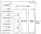
- FIG. 1 is a schematic diagram showing a configuration of a color sensor (sensor) 1 according to the first embodiment of the present invention.
- the color sensor 1 includes a color detection region D (C) for detecting visible light and an infrared detection region D (IR) for detecting infrared light.
- the color detection area D (C) includes a red detection area (specific color detection area) D (R) for detecting red (R) and a green detection area (specific color for detecting green (G).
- the red detection region D (R), the green detection region D (G), the blue detection region D (B), and the infrared detection region D (IR) have the same area.
- region may be arrange
- the analog-digital conversion circuit ADC has a function of performing analog-digital conversion on the current output from the detection region and outputting a digital signal to the storage circuit unit 11. It is preferable that each analog-digital conversion circuit ADC has the same circuit configuration.
- an artificial light source fluorescent lamp, incandescent lamp, etc.
- a general AC power source is 50 Hz / The 60 Hz frequency component can be effectively removed.
- the memory circuit unit 11 has a function of recording a digital value proportional to the magnitude of a digital signal obtained by analog-to-digital conversion of the current output from each detection area.
- the storage circuit unit 11 may be configured by a general register circuit or flash memory, but is not limited to this configuration.
- an arithmetic circuit is incorporated in the memory circuit unit 11 so that the output value from each detection region is converted into the tristimulus values (XYZ) described above and further recorded (saved) in the memory circuit unit 11.
- the chromaticity diagram may be converted and the correlated color temperature may be calculated and recorded. Further, the result calculated in the arithmetic circuit may be output to the outside.
- the external output circuit unit 12 is a circuit for outputting the data stored (saved) in the storage circuit unit 11 to a display device on which the color sensor 1 is mounted.
- the output may be a general I2C serial data output or a parallel data output, but is not limited to this configuration.
- a control circuit such as an oscillator or a DSP may be separately used.
- FIG. 2 is a vertical structure diagram illustrating an example of the specific color detection region and the infrared detection region.
- the specific color detection region and the infrared detection region are formed on the semiconductor substrate.
- the specific color detection area is any one of the red detection area D (R), the green detection area D (G), and the blue detection area D (B).
- the specific color detection region is the red detection region D (R)
- the specific color detection region includes the infrared cut filter IRCutF, the interlayer film IM, and the red filter (first specific color filter) CF ( R) and a light receiving element portion (first light receiving element portion) PDS, and light enters from the outside in this order.
- the red filter CF (R) is a green filter (first specific color filter) CF (G).
- the red filter CF (R) is a blue filter (first specific color filter) CF (B).
- the infrared detection region D includes an infrared cut filter IRCutF, an interlayer film IM, a blue filter (second specific color filter) CF (B), and a light receiving element unit (first 2 light receiving element portions) PDS, and light enters from the outside in this order.
- each detection region includes a light receiving element portion PDS.
- the light receiving element portion PDS can be regarded as a combination of photodiodes (PD: PhotoDiode) as described later.
- the various filters such as the red filter CF (R), the green filter CF (G), and the blue filter CF (B) are preferably composed of on-chip general dye-based filters in terms of cost.
- the red filter CF (R) is a filter that transmits red (first specific color) light.
- the green filter CF (G) is a filter that transmits green (first specific color) light.
- the blue filter CF (B) is a filter that transmits blue (first specific color, second specific color) light.
- the infrared cut filter IRCutF may be either an on-chip configuration or an infrared cut glass, but preferably has a configuration in which the entire surface of the specific color detection region and the infrared detection region D (IR) are uniformly covered. . Further, assuming that the color sensor of the present invention is composed of an on-chip infrared cut filter IRCutF, the device has been devised to facilitate manufacturing as described later.
- the infrared detection region D has a configuration in which a blue filter CF (B) and an infrared cut filter IRCutF are vertically stacked.
- the spectral sensitivity characteristic of the photodiode is characterized by having a peak sensitivity in the infrared component. Since a typical Si photodiode has a peak sensitivity in the infrared component, for example, if the upper surface of the Si photodiode is shielded by gate polysilicon, the visible light is cut and the infrared light is transmitted to some extent. Can be created easily.
- the infrared cut filter IRCutF and the specific color detection filter Is subjected to photoelectric conversion by a photodiode (visible light receiving element, infrared light receiving element), and a current (current signal) corresponding to the received light is output.
- the output may be used as an analog current signal, or may be used as a digital signal after undergoing analog-digital conversion.
- the configurations of the infrared cut filter IRCutF and the specific color filter are not limited to the configurations described above.
- the infrared cut filter IRCutF is preferably protected because it is more expensive than the specific color filter. Therefore, as shown in FIG. 3, the stacking order of the infrared cut filter IRCutF and the specific color filter may be reversed with respect to the incident direction of light incident from the outside as compared with the configuration of FIG. That is, in each detection region, a configuration in which light is incident from the outside in the order of the specific color filter, the interlayer film IM, the infrared cut filter IRCutF, and the light receiving element portion PDS may be employed.
- the specific color filter in the infrared detection region is not limited to the configuration using the blue filter CF (B).
- a black filter in which a red filter CF (R) and a blue filter CF (B) are stacked may be used.
- a difference occurs in the cross-sectional structure of the region.
- the infrared cut filter IRCutF is distorted, and there is a possibility that the consistency of the incident position of light from the outside deteriorates.
- crosstalk can increase in adjacent detection areas.
- cost of the additional specific color filter and the flattening process of the interlayer film IM for example, when forming the interlayer film IM before applying the infrared cut filter IRCutF on the top of the stacked body Manufacturing costs may increase.
- the color sensor 1 according to the embodiment of the present invention has no difference between the cross-sectional structure of the infrared detection region D (IR) and the cross-sectional structure of the specific color detection region, the above-described crosstalk and manufacturing costs increase. do not do.
- Light receiving element part PDS (Light receiving element part PDS) Below, the structure of the light receiving element part PDS in each detection area
- the light receiving element portion PDS is made of a P substrate (Psub).
- P substrate In the P substrate, an N well (Nwell) and a P diffusion layer (Pdif) formed in the N well are formed.
- a photodiode (infrared light receiving element) PDir is formed in a junction region between the P substrate and the N well.
- a photodiode (visible light receiving element) PDvis is formed in the junction region between the N well and the P diffusion layer.
- the photodiode PDir is formed at a deep position of the P substrate when viewed from the incident direction of light incident on the light receiving element portion from the outside, this is called a deep junction.
- the photodiode PDvis is formed at a shallow position of the P substrate as viewed from the incident direction, this can be called a shallow junction.
- the surface of the P substrate on which light from the outside is incident is referred to as a P substrate surface.
- a red filter CF (R), a green filter CF (G), a blue filter CF (B), or an infrared cut filter IRCutF is applied to the P substrate surface.
- an interlayer film, a wiring layer, and the like are provided between the P substrate surface and the specific color filter. That is, the wiring of the photodiode PDir and the connection of the photodiode PDvis shown in FIG. 2 are performed in the wiring layer.
- the anode of the photodiode PDir and the anode of the photodiode PDvis in the specific color detection region are connected to GND.
- the cathode of the photodiode PDir and the cathode of the photodiode PDvis are connected to each other.
- a current Iall that combines the light reception current Iir in the photodiode PDir and the light reception current Ivis in the photodiode PDvis flows at the connection point between the cathode of the photodiode PDir and the cathode of the photodiode PDvis. That is, from the specific color detection region, the respective light receiving currents of the photodiode PDvis and the photodiode PDir having different junction depths are summed and output.
- the infrared detection region D is connected to the cathode of the photodiode PDir instead of grounding the anode of the photodiode PDvis. In this way, by short-circuiting the anode and cathode of the photodiode PDvis, only the light reception current Iir in the photodiode PDir is output from the infrared detection region D (IR).
- the photodiode PDvis formed in the shallow junction portion and the photodiode PDir formed in the deep junction portion generally have the spectral sensitivity characteristics. Is different. Hereinafter, the difference in spectral sensitivity characteristics will be described.
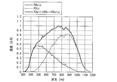
- FIG. 4 is a graph showing an example of spectral sensitivity characteristics of the shallow junction photodiode PDvis and the deep junction photodiode PDir.
- the thin solid line indicates the spectral sensitivity characteristic of the photodiode PDvis.
- a broken line indicates the spectral sensitivity characteristic of the photodiode PDir.
- a thick solid line indicates the total of the spectral sensitivity characteristic of the photodiode PDvis and the spectral sensitivity characteristic of the photodiode PDir.
- the photodiode PDvis having a shallow junction has sensitivity up to the infrared component with a peak in the visible light region
- the photodiode PDir having a deep junction has peak sensitivity in the infrared light region.
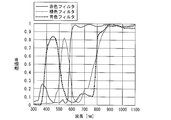
- FIG. 5 is a graph showing the spectral sensitivity characteristics of a general color filter.
- the solid line indicates the spectral sensitivity characteristic of the red filter CF (R).
- a dotted line indicates a spectral sensitivity characteristic of the green filter CF (G).
- a broken line indicates the spectral sensitivity characteristic of the blue filter CF (B).
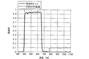
- FIG. 6 is a graph showing the spectral sensitivity characteristics of a general infrared cut filter IRCutF.
- the solid line indicates the spectral sensitivity characteristic of the infrared cut filter IRCutF when the infrared light (IR) is completely cut.
- the broken line is the spectral sensitivity characteristic of the infrared cut filter IRCutF when 10% of the infrared component is transmitted.
- FIG. 7 is a graph showing spectral sensitivity characteristics in the red detection region D (R), the green detection region D (G), the blue detection region D (B), and the infrared detection region D (IR).
- the red detection characteristic has a peak sensitivity in the red component.
- the green detection characteristic has a peak sensitivity in the green component.
- the blue detection characteristic has a peak sensitivity in the blue component.
- the blue filter CF (R) having the spectral sensitivity characteristic shown in FIG. 5 and the infrared cut filter IRCutF having the spectral sensitivity characteristic when transmitting the infrared component indicated by the broken line in FIG. 6 by 10% are stacked.
- the blue filter CF (R) having the spectral sensitivity characteristic shown in FIG. 5 and the infrared cut filter IRCutF having the spectral sensitivity characteristic when transmitting the infrared component indicated by the broken line in FIG. 6 by 10% are stacked.
- the sensitivity characteristics of each specific color detection area and the spectral sensitivity characteristics of the infrared detection area D (IR) are similar to the spectral sensitivity characteristics of the respective infrared components of each specific detection area. It has characteristics. Thereby, only the infrared component can be obtained by subtracting the output signal of the infrared detection region D (IR) from the output signal of each specific color detection region.
- the sensitivity of the infrared cut filter IRCutF increases by about 10% in the infrared wavelength region (775 nm to 1100 nm) due to manufacturing variations of the infrared cut filter IRCutF, it is also incorporated into the display device.
- the spectral transmittance of the panel arranged in front of the color sensor 1 is different between the visible region and the infrared region, the output signal from the specific color detection region and the infrared detection region D (IR) By calculating this signal, accurate color temperature and illuminance can be output.
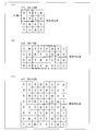
- FIG. 8 is a top view showing a method for arranging the detection areas of the respective colors.
- the color sensor 1 includes a set of four different types of detection areas, which are composed of three specific color detection areas and infrared detection areas having three different specific colors, red, green, and blue. If one is provided, the minimum operation is possible.
- the light incident on the color sensor 1 is not uniformly irradiated like the light emitted from the surface light source, but is irradiated unevenly like the light emitted from the point light source, and at a certain angle (directivity). Corners).
- the color sensor 1 is irradiated with the non-uniform light, the color temperature and illuminance that are finally output by calculation may not be accurate.
- nonuniform irradiation is performed by arranging 4n sets (n is a natural number) of the above-described four different types of detection areas so as to be point-symmetric with respect to a preset light receiving center point.
- n is a natural number
- R represents the red detection region D (R).
- G represents the green color detection region D (G).
- B represents the blue color detection region D (B).
- IR represents the infrared detection region D (IR).
- one red detection area D (R), one green detection area D (G), one blue detection area D (B), and 1 Infrared detection regions D (IR) are arranged in 2 rows and 2 columns to form one set S. Then, 4n sets (n is a natural number) are arranged so as to be point-symmetric with respect to the light receiving center point.
- each detection area closest to the light receiving center point is arranged in the clockwise direction as R, G, B, IR, but is not limited to this configuration.
- each detection area may be rotated and arranged with respect to the light receiving center point, or the detection areas having a diagonal positional relationship such as R and B, G and IR may be replaced, and further adjacent to each other.
- the detection area may be exchanged. That is, it is important to ensure the symmetry of the above set with respect to the light receiving center point, and there is no restriction on the arrangement of the four types of detection areas close to the center. In addition, at this time, it is only necessary that the types of adjacent detection regions are arranged so as not to overlap each other.
- G and IR are arranged on an oblique line from the upper left to the lower right
- R and B are arranged on an oblique line from the upper right to the lower left.
- any row or any column there is a pattern in which R, G, B, and IR are combined one by one.
- the detection areas are arranged in 4 rows ⁇ 8 columns.
- the color sensor 1 is composed of four types of detection regions, it is important for the above-described light uniformity that each row and each column is composed of multiple detection regions of four. It can be said that there is.
- the detection region 1 if the detection region is added so as to lie on an oblique line, the arrangement is point-symmetric with respect to the light receiving center point.
- each detection area is arranged in 8 rows ⁇ 8 columns.
- each detection region is arranged so that the entire shape of the detection areas is a square.
- the arrangement is point-symmetric with respect to the light receiving center point.
- FIG. 9 is a diagram showing a configuration of the analog-digital conversion circuit ADC.
- the analog-digital conversion circuit ADC includes a charging circuit (integrating circuit) 15, a discharging circuit 16, a comparison circuit 17, and a control circuit (output circuit) 18.
- a charging circuit integrating circuit
- a discharging circuit a comparison circuit
- a control circuit output circuit
- FIG. 1 there are a plurality of analog-digital conversion circuits ADC corresponding to each specific color detection region and infrared detection region, but these have the same configuration.
- the present invention is not limited to this configuration.
- the configuration of some analog-digital conversion circuits ADC may be changed.
- the charging circuit 15 includes an amplifier AMP1 constituting an integrator and a capacitor (integrating capacitor) C1. An amount of electric charge corresponding to the input current Iin is stored in the capacitor C1.
- the discharge circuit 16 includes a power supply Vdd, a reference current source Iref that generates a reference current IREF for discharging the charge stored in the capacitor C1, and a switch SW2 for switching ON / OFF of discharge.
- the comparison circuit 17 includes a comparator CMP1 and a switch SW1.
- the comparator CMP1 compares the output voltage Vsig of the charging circuit 15 and the reference voltage Vref supplied from the reference voltage source V1, and outputs an output signal comp.
- the data conversion period in which the input current Iin that is input is converted into the digital value ADCOUT is determined by ON / OFF of the switch SW1.
- the switch SW1 when the switch SW1 is turned on, the reference voltage source V1 is connected to the charging circuit 15, the reference voltage Vref is supplied to the capacitor C1, and the capacitor C1 is charged.
- the comparator CMP1 When the switch SW1 is turned off, the output voltage Vsig of the charging circuit 15 and the reference voltage Vref are compared by the comparator CMP1.
- the comparison output signal comp is input to the control circuit as a binary pulse signal of “High” and “Low”.
- An input current Iin that is input while the switch SW1 is OFF is converted to a digital value ADCOUT.
- the control circuit 18 includes a flip-flop FF and a counter COUNT.
- the output signal comp of the comparison circuit 17 is latched by the flip-flop FF.
- the bit stream signal charge is input to the discharge circuit 16 and the counter COUNT, respectively.
- the counter COUNT counts the number of LOW levels (the number of discharges) of the bit stream signal charge. That is, the counter COUNT counts active pulses.
- the count result is output as a digital value ADCOUT that is an analog-digital conversion value corresponding to the input current Iin that has been input.
- the switch SW2 of the discharge circuit 16 is turned ON / OFF based on the bit stream signal charge.
- the switch SW2 of the discharge circuit 16 is turned on, electric charge is stored in the capacitor C1 of the charging circuit 15 by the discharge circuit 16.
- the switch SW2 is turned off, the charge of the capacitor C1 of the charging circuit 15 is discharged according to the input current Iin that is input.
- FIG. 10 is a waveform diagram showing the operation of the analog-digital conversion circuit ADC.
- the switch SW2 when a high level signal is input to the switch SW2, the switch SW2 is turned off, and the charge stored in the capacitor C1 of the charging circuit 15 is discharged according to the input current Iin (precharge operation). As a result, the output voltage Vsig of the charging circuit 15 decreases.
- the output voltage Vsig of the charging circuit 15 and the reference voltage Vref are set in the same manner, the output voltage Vsig of the charging circuit falls below the reference voltage Vref during this period.
- the switch SW2 When a low level signal is input to the switch SW2, the switch SW2 is turned on, and the capacitor C1 of the charging circuit 15 is charged by the discharging circuit 16 with the electric charge. As a result, the output voltage Vsig of the charging circuit 15 increases. At some point, the output voltage Vsig of the charging circuit 15 exceeds the reference voltage Vref.
- the output voltage Vsig of the charging circuit 15 and the reference voltage Vref are compared by the comparator CMP1, and when the output voltage Vsig of the charging circuit 15 exceeds the reference voltage Vref, a high level output signal comp is output from the comparator CMP1. .
- the flip-flop FF latches the output signal comp, and in synchronization with the rise of the next clock signal clk, the high-level bit stream signal charge. Is output.
- the switch SW2 When the high-level bit stream signal charge is input to the switch SW2, the switch SW2 is turned off, and the charge stored in the capacitor C1 of the charging circuit 15 is discharged. As a result, the output voltage Vsig of the charging circuit 15 decreases. At some point, the output voltage Vsig of the charging circuit 15 falls below the reference voltage Vref. When the output voltage Vsig of the charging circuit 15 falls below the reference voltage Vref, a low level output signal comp is output as an active pulse indicating that the output of the comparator CMP1 is at the active level. Note that the active pulse may be set to either the Low level or the High level, and can be appropriately selected depending on the operation logic of the circuit.
- the flip-flop FF latches the output signal comp so that the control circuit 18 takes in the output signal comp, and the flip-flop FF A low-level bit stream signal charge is output in synchronization with the rise of the signal clk.
- the switch SW2 When a low-level bit stream signal charge is input to the switch SW2, the switch SW2 is turned on.
- the bit stream signal charge is a time-series arrangement of low level signals (active pulses), and the switch SW2 is turned on during the low level period (active pulse period).
- the analog-digital conversion circuit ADC repeats the above operation, and the counter COUNT counts the number of discharges count of the discharge circuit 16 during the period when the switch SW1 is OFF, that is, the data conversion period t_conv. It is possible to output the digital value ADCOUT corresponding to the input current Iin.
- the amount of charge charged by the input current Iin in the data conversion period t_conv is, assuming that the period of the clock signal clk is t_clk.
- the minimum resolution of the analog-digital conversion circuit ADC is determined by (IREF ⁇ t_clk).
- Is set to count (Iin / IREF) ⁇ 2 n (7) Is guided.
- the integration type analog-digital conversion circuit ADC can perform analog-digital conversion with a wide dynamic range and high resolution.
- the memory circuit unit 11 shown in FIG. 1 may be configured to take in (record) the output signal of ADCOUT at the timing when the set integration time ends.
- the signal output value of each color of red, green, and blue directly converted from analog to digital by the analog-to-digital conversion circuit ADC and from the infrared region.
- ADC analog-to-digital conversion circuit
- the input voltage to the non-inverting input terminal of the amplifier AMP1 can be set to 0V.
- the voltage across the photodiode bias voltage
- the dark current of the photodiode it is possible to accurately measure even a low light amount. That is, measurement with low sensitivity can be performed accurately.
- color information output and infrared information output are controlled and output in time series, which leads to a reduction in circuit scale.
- the output from each detection region is connected to a multiplexer and connected to the input of one ADC.
- the output current is selected by a multiplexer every 10 msec, sequentially output, and the information is recorded in an internal register.
- the color sensor can obtain all accurate color information.
- FIG. 11 is a block diagram illustrating a schematic configuration of the display device 2 according to the present embodiment.
- the display device 2 includes a color sensor 1, a backlight control unit 21, a backlight 22, and a display panel 25.
- the backlight 22 is a light source for irradiating the display panel 25 that displays a screen from the back side, and includes, for example, a red LED, a green LED, and a blue LED.
- the color sensor 1 receives the ambient light of the display device 2, measures the color component of the ambient light, and outputs a digital signal DOUT to the backlight control unit 21 as a measurement result. That is, the color sensor 1 outputs illuminance information based on the output signal of the color detection region (specific color detection region) D (C) and the output signal of the infrared detection region D (IR). Next, the backlight control unit 21 calculates a color component and illuminance by calculating from the digital signal (illuminance information) DOUT.
- the brightness of the red LED, the green LED, and the blue LED of the backlight 22 is controlled to control the color of the backlight 22 according to the color component of the ambient light or The brightness can be controlled.
- the backlight control unit 21 controls to increase the luminance of the backlight 22, and when the illuminance of the ambient light is small, the backlight control unit 21 decreases the luminance of the backlight 22. To control. Thereby, the power consumption of the backlight 22 can be suppressed, and the color of the display panel 25 can be accurately controlled so as to correspond to the eye color adaptation.
- FIG. 12 is a block diagram showing a schematic configuration of the memory circuit unit 11 according to the present embodiment.
- the storage circuit unit 11 is roughly divided into a storage circuit control unit 110, a memory 111, a communication unit 112, and an input unit 113.
- the storage circuit control unit 110 is a main component of the storage circuit unit 11 and receives digital values of each color from the analog-digital conversion circuit ADC shown in FIG. Or the illuminance is output to the external output circuit unit 12.
- the memory 111 stores correction matrix data 1111 and the like.
- the memory 111 may store digital values for each color.
- the storage circuit control unit (storage circuit control unit) 110 includes a tristimulus value calculation unit (tristimulus value calculation unit) 1101, a correction matrix setting unit 1102, a color temperature calculation unit (color temperature calculation unit) 1103, and an illuminance calculation.
- the tristimulus value calculator 1101 calculates tristimulus values based on the R, G, B, and IR digital values output from the analog-digital conversion circuit ADC shown in FIG.
- the tristimulus values can be calculated by multiplying the correction matrix and a vector made up of each digital value, as shown in the above equation (2).
- the tristimulus value calculation unit 1101 is connected to the correction matrix setting unit 1102, receives the correction matrix from the correction matrix setting unit 1102, and uses it for calculation of the tristimulus values.
- the tristimulus value calculation unit 1101 is connected to the color temperature calculation unit 1103, the illuminance calculation unit 1104, and the output selection unit 1105.
- the correction matrix setting unit 1102 sets a correction matrix used in the tristimulus value calculation unit 1101 to calculate tristimulus values.
- the correction matrix setting unit 1102 is connected to the memory 111 and receives the correction matrix data stored from the memory 111.
- correction matrix setting unit 1102 may be connected to the communication unit 112 and receive correction matrix data from the external network 3 via the communication unit 112. Further, the received correction matrix data may be stored in the memory 111.
- correction matrix setting unit 1102 may be connected to the input unit 113, and may receive the input from the input unit 113 and manually update the correction matrix. Further, the updated correction matrix data may be stored in the memory 111.
- correction matrix setting unit 1102 is not limited to the above-described configuration, and may be integrated in the tristimulus value calculation unit 1101.
- the color temperature calculation unit 1103 calculates the color temperature from the tristimulus values obtained from the tristimulus value calculation unit 1101.
- the illuminance calculation unit 1104 calculates illuminance from the tristimulus values obtained from the tristimulus value calculation unit 1101.
- the color temperature calculation unit 1103 and the illuminance calculation unit 1104 are connected to the output selection unit 1105, respectively.
- the output selection unit 1105 selects the tristimulus value obtained from the tristimulus value calculation unit 1101, the color temperature obtained from the color temperature calculation unit 1103, or the illuminance obtained from the illuminance calculation unit 1104.
- the output selection unit 1105 is connected to the external output circuit unit 12 and transmits the selected value.
- the tristimulus value calculation unit 1101 uses R, G, and B output from the analog-digital conversion circuit ADC shown in FIG. 1 as tristimulus values by using a row example similar to a unit matrix as a correction matrix.
- the digital value can be transmitted to the output selection unit 1105 as it is.
- the matrix similar to the unit matrix is a matrix in which C 11 , C 22 , and C 33 are 1 and the other coefficients are 0 in Equation (2).
- the output selection unit 1105 can transmit the R, G, and B digital values, the tristimulus values, the color temperature, and the illuminance to the external output circuit unit 12.
- the color sensor 1 can self-diagnose such deterioration of components.
- a configuration for performing self-diagnosis when the color sensor 1 is deteriorated from the factory shipment (reference time) state will be described.
- the memory 111 further stores a factory shipment value (reference value) 1112 of the digital value of each color with respect to the reference sample.
- a reference sample is a sample that can exhibit a constant tristimulus value, color temperature, or illuminance that can be used as a reference over a long period of time.
- the factory shipment value 1112 is a digital value of each color that can be acquired when the reference sample is sensed by the color sensor 1 at the time of factory shipment.
- a digital value that can be acquired when the reference sample is sensed by the color sensor 1 at the time of shipment from the factory and a digital value that is obtained when the reference sample is sensed by the color sensor 1 that has passed the time after shipment from the factory. If this value is changed, it can be determined that the component of the color sensor 1 has deteriorated.
- the self-diagnosis can be performed by comparing the factory shipment value stored in the memory 111 with the digital value for the reference sample.
- the color sensor in order to detect the color temperature of ambient light, includes red, green, and blue detection areas as specific color detection areas that are sensitive to light of a specific color in visible light.
- the present invention is not limited to this. Instead of the red, green, and blue detection areas, for example, areas for detecting cyan, magenta, and yellow colors may be provided.
- the number of specific color detection areas is not particularly limited. For example, only one specific color detection region is provided, and a signal indicating the true color information of the specific color is output from the output signal of the specific color detection region based on the output signal of the infrared detection region and the signal of the specific color. Obtainable. Thus, a specific color component of ambient light can be accurately detected, and an inexpensive and small color sensor can be provided.
- the sensor according to aspect 1 of the present invention includes a specific color detection region having sensitivity to light of a specific color in visible light, and an infrared detection region having sensitivity to infrared light, and the specific color detection region. Passes through the first specific color filter that transmits light of the first specific color, the infrared cut filter that cuts infrared components from the light, the first specific color filter, and the infrared cut filter A first light receiving element portion that receives the received light, and the infrared detection region includes a second specific color filter that transmits light of a second specific color, the infrared cut filter, and the second And a second light receiving element portion that receives light transmitted through the infrared cut filter, and an output signal of the first light receiving element portion in accordance with an output signal of the second light receiving element portion It is characterized by subtracting the infrared component from.
- the specific color filter may be, for example, a red filter, a green filter, or a blue filter.
- a signal corresponding to light of a specific color is output from the specific color detection region, and a signal corresponding to infrared light is output from the infrared detection region.
- the output signal of the specific color detection region includes not only a specific color component but also an infrared component that cannot be cut by the infrared cut filter. If the color sensor has such an infrared component, accurate color temperature and illuminance information cannot be output.
- the color of the true specific color Information can be obtained, whereby accurate color temperature and illuminance information can be output.
- the color temperature and illuminance can be accurately calculated even when it is necessary to use an infrared cut filter that transmits the infrared component to some extent.
- the layered state of the filters can be made uniform. It becomes possible. Thereby, in manufacture of a sensor, a planarization process etc. become unnecessary, for example, and cost can be suppressed.
- the thickness of the infrared cut filter can be made uniform, and the infrared component of the light irradiated to the light receiving element portion in each specific color detection region and the infrared detection region can be made uniform. it can.
- the second specific color is blue.
- the second specific color is blue
- a blue filter is used as the specific color filter in the infrared detection region.
- a red filter or a green filter in addition to the blue filter as the specific color filter in the infrared detection region.
- the spectral sensitivity characteristics of the red filter can include a red component close to the infrared component. It is also known that the spectral sensitivity characteristic of the green filter does not include an infrared component.
- the red filter or the green filter is used as the specific color filter in the infrared detection region, it is considered that the output signal in the infrared detection region does not accurately reflect the infrared component. That is, as described above, it is considered impossible to obtain color information of the true specific color by removing the infrared component from the output signal of the specific color detection area using the output signal of the infrared detection area. It is done.
- the red detection sensitivity in the infrared detection region can be reduced compared to the case where a red filter or a green filter is used. In this configuration, only the infrared component is sensitive.
- the output signal of the infrared detection region can reflect the infrared component more correctly when the blue filter is used than when the other specific color filter is used.
- the first specific color is preferably red, green, or blue.
- a sensor capable of detecting red, green, or blue color components can be provided.
- the specific color filter, the infrared cut filter it is preferable that the light receiving element portion is arranged.
- the filter may be deteriorated by ultraviolet rays contained in the irradiated light or physical external force.
- the infrared cut filter is more expensive than the specific color filter, it is preferable that the infrared cut filter be protected.
- the light emitted from the outside passes through the specific color filter before passing through the infrared cut filter. Therefore, since ultraviolet rays are first absorbed by the specific color filter, deterioration of the infrared cut filter due to the ultraviolet rays can be suppressed. In addition, since the physical external force first acts on the specific color filter, it is possible to suppress the deterioration of the infrared cut filter due to the physical external force.
- each light receiving element unit includes a visible light receiving element having a peak of sensitivity in the visible light region and an infrared light region.
- An infrared light receiving element having a sensitivity peak, and in the first light receiving element portion, the cathode of the visible light receiving element and the cathode of the infrared light receiving element are connected to each other.
- the cathode and the anode of the visible light receiving element are short-circuited.
- the current obtained by adding the light receiving current of the visible light receiving element and the light receiving current of the infrared light receiving element is And output from the first light receiving element section.
- the specific color detection region includes the first light receiving element portion. Therefore, the current is output from the specific color detection area.
- the cathode and the anode of the visible light receiving element are short-circuited, only the light receiving current of the infrared light receiving element is output from the second light receiving element unit.
- the infrared detection region includes the second light receiving element portion. Therefore, the received light current is output from the infrared detection region.
- a current signal corresponding to light of a specific color is output from the specific color detection region, and a current signal corresponding to infrared light is output from the infrared detection region. Therefore, by using the current signal in the infrared detection region, the infrared component can be removed from the current signal in the specific color detection region, and color information of the true specific color can be obtained.
- n is a natural number
- each specific color detection region and the infrared detection region have the same area
- each set is point-symmetric with respect to a preset light receiving center point. It is preferable that the specific color detection regions that are arranged and have sensitivity to light of the same specific color are not adjacent to each other, and the infrared detection regions are not adjacent to each other.
- the areas of the detection areas forming the set are equal, the light received by each detection area can be made uniform, and the color components can be detected accurately.
- each set symmetrically with respect to the light receiving center, the amount of light received by each specific color detection region and infrared detection region can be made uniform with respect to the light incident on the sensor.
- the specific color detection areas sensitive to the same specific color light are not adjacent to each other, and the infrared detection areas are not adjacent to each other, so that each specific color detection area and the infrared detection area receive light. The amount of light can be made more uniform.
- the senor can be made insensitive to the incident angle of light incident on the sensor, and can be made independent of the incident angle.
- each specific color detection area and infrared detection area is at least 16 or more. This number is a number that can sufficiently equalize the amount of light received by each specific color detection region and infrared detection region.
- the specific color detection region and the infrared detection region output a current signal corresponding to light reception, and the current signal It is preferable to further include an analog-to-digital conversion circuit that performs analog-to-digital conversion into a digital signal, and a storage circuit unit that stores a digital value proportional to the magnitude of each digital signal.
- the fluctuation component of a light source generally driven by an AC power supply of 50 Hz / 60 Hz can be averaged by making the analog-digital conversion circuit an integration type and setting the integration time to 10 msec or more. Output results with high accuracy.
- a display device on which a sensor according to the present invention is mounted includes a CPU and can often perform digital signal processing. That is, by using the sensor according to the present invention, it is possible to reduce the number of parts for digital signal processing required in an analog-digital conversion circuit or the like. That is, the sensor according to the present invention is suitable as a sensor mounted on a display device.
- the digital value stored by the storage circuit can be converted into a tristimulus value, a correlated color temperature, or the like by digital processing and further stored.
- the correlated color temperature may be converted using a color temperature diagram.
- the storage circuit unit includes tristimulus value calculation means for calculating tristimulus values from each digital value and the correction matrix, and a memory for storing the correction matrix. It is preferable to comprise.
- the memory provides the stored correction matrix to the tristimulus value calculation means. Then, the tristimulus value calculating means can obtain a vector of tristimulus values by multiplying the vector obtained from each digital value and the correction matrix.
- the storage circuit unit includes a color temperature calculation unit that calculates a color temperature from the tristimulus values, and an illuminance calculation that calculates illuminance from the tristimulus values. It is preferable to further comprise means and output selection means for selecting the tristimulus value, the color temperature, or the illuminance and transmitting them to the outside.
- the color temperature calculation means can calculate the color temperature from the tristimulus values obtained from the tristimulus value calculation means.
- the illuminance calculation means can calculate illuminance from the tristimulus values.
- the output selection means can select a tristimulus value, a color temperature, or an illuminance and transmit it to the outside.
- the tristimulus value calculation means uses a matrix similar to the unit matrix as the correction matrix, thereby transmitting the digital values of the respective colors (R, G, and B) as tristimulus values as they are to the output selection means. be able to. Therefore, the output selection means can transmit the digital value, tristimulus value, color temperature, and illuminance of each color to the external output circuit unit.
- the memory further stores a reference value that is a digital value for the reference sample acquired at the time of reference
- the tristimulus value calculation means includes: The self-diagnosis is preferably performed by comparing the reference value with a digital value for a reference sample acquired after the reference time.
- the digital value input to the memory circuit changes even for the same sensing object.
- the digital value (reference value) obtained when the reference sample is sensed by the sensor at the reference time is stored in the memory. Then, by comparing the reference value with the digital value obtained when the reference sample is sensed by the sensor when the time has elapsed from the reference time, the change in the digital value due to the deterioration of the sensor components is detected. Can grasp and self-diagnose.
- a reference value is compared with a digital value at a certain time, and when a predetermined determination criterion is exceeded, it can be determined by self-diagnosis that repair is necessary.
- the analog-digital conversion circuit includes an integration capacitor that stores electric charge according to the current signal, and a voltage corresponding to an amount of electric charge stored by the integration capacitor. Is compared with the output voltage of the integration circuit and the reference voltage, and the comparison result is output as a binary pulse signal. The pulse signal is synchronized with the clock signal.
- a flip-flop that captures and outputs a bitstream signal, and a counter that counts the active pulses of the bitstream signal, and an output circuit that outputs a counting result by the counter as an output value of the analog-digital conversion circuit; Integrate by outputting current during the active pulse period of the bitstream signal It is preferably a digital conversion circuit - integrating analog and a discharge circuit that discharges the capacitor.
- the total length of the active pulse period depends on the magnitude of the current signal. Then, the output pulse current of the output circuit is integrated (that is, averaged) by the integration circuit, so that an analog-digital converted signal can be obtained with a simple configuration.
- a bias voltage is not applied to the visible light receiving element and the infrared light receiving element.
- the dark current of the visible light receiving element and the infrared light receiving element can be suppressed, and measurement with low sensitivity can be performed accurately.
- the display device includes a display panel that displays a screen, a backlight that irradiates the display panel, a backlight control unit that controls the backlight, and the sensor.
- the backlight control unit controls the color of the backlight based on a signal output from the sensor according to any one of the first to twelfth aspects.
- the display device since the display device includes the sensor that can accurately detect the color component of the ambient light, the display panel screen color can be accurately suppressed so as to correspond to the color adaptation of the eyes. Can do.
- the sensor outputs illuminance information based on the output signal of the specific color detection area and the output signal of the infrared detection area, and the backlight. It is preferable that the control unit controls the luminance of the backlight based on the illuminance information.
- the display apparatus since the display apparatus is equipped with the sensor which can detect the color component (illuminance information) of ambient light correctly, it controls the brightness of a screen correctly according to the illumination intensity of ambient light. Can do.
- control program can cause the computer to function as each means included in the memory circuit unit according to any one of the above-described aspects 8 to 10. Furthermore, by storing the control program in a computer-readable recording medium, the control program can be executed on a general-purpose computer.
- Each block of the storage circuit unit 11 of the color sensor 1, particularly the storage circuit control unit 110, may be configured by hardware logic, or may be realized by software using a CPU as follows.
- the storage circuit unit 11 includes a storage device (such as a CPU that executes instructions of a control program that realizes each function, a ROM that stores the program, a RAM that expands the program, a memory that stores the program and various data, and the like. Recording medium).
- An object of the present invention is a recording medium on which a program code (execution format program, intermediate code program, source program) of a control program of the storage circuit unit 11 which is software for realizing the above-described functions is recorded so as to be readable by a computer. This can also be achieved by supplying the data to the storage circuit unit 11 and reading and executing the program code recorded on the recording medium by the computer (or CPU or MPU).
- Examples of the recording medium include tapes such as magnetic tapes and cassette tapes, magnetic disks such as floppy (registered trademark) disks / hard disks, and optical disks such as CD-ROM / MO / MD / DVD / CD-R.
- Card system such as IC card, IC card (including memory card) / optical card, or semiconductor memory system such as mask ROM / EPROM / EEPROM (registered trademark) / flash ROM.
- the storage circuit unit 11 may be configured to be connectable to a communication network, and the program code may be supplied via the communication network.
- the communication network is not particularly limited.
- the Internet intranet, extranet, LAN, ISDN, VAN, CATV communication network, virtual private network, telephone line network, mobile communication network, satellite communication. A net or the like is available.
- the transmission medium constituting the communication network is not particularly limited. For example, even in the case of wired such as IEEE 1394, USB, power line carrier, cable TV line, telephone line, and ADSL line, infrared rays such as IrDA and remote control, Bluetooth (Registered trademark), 802.11 wireless, HDR, mobile phone network, satellite line, terrestrial digital network, and the like can also be used.
- the color sensor according to the present invention can detect chromaticity with high accuracy, it can be suitably used for a display device.
Landscapes
- Physics & Mathematics (AREA)
- General Physics & Mathematics (AREA)
- Engineering & Computer Science (AREA)
- Spectroscopy & Molecular Physics (AREA)
- Computer Hardware Design (AREA)
- Theoretical Computer Science (AREA)
- Chemical & Material Sciences (AREA)
- Crystallography & Structural Chemistry (AREA)
- Nonlinear Science (AREA)
- Mathematical Physics (AREA)
- Optics & Photonics (AREA)
- Spectrometry And Color Measurement (AREA)
- Testing Of Optical Devices Or Fibers (AREA)
- Liquid Crystal (AREA)
Abstract
Description


Y = C21×R+C22×G+C23×B+C24×IR …(3)
ここで、色検出領域の感度より赤外検出領域の感度が高くなる場合には、補正マトリックスのCx4×IRの項が大きくなる。このため、三刺激値を算出する際、減算項が大きくなるので、減算にともなう誤差が大きくなり、当該計算式を利用する方式によるカラーセンサでは、色温度や照度の出力精度が悪化する。
本発明の第1の実施形態について、図1~図10に基づいて詳細に説明すると以下の通りである。
図1は、本発明の第1の実施形態に係るカラーセンサ(センサ)1の構成を示す模式図である。図1に示すように、カラーセンサ1は、可視光を検出するための色検出領域D(C)と、赤外光を検出するための赤外検出領域D(IR)とを備えている。ここで、色検出領域D(C)は、赤色(R)を検出するための赤色検出領域(特定色検出領域)D(R)、緑色(G)を検出するための緑色検出領域(特定色検出領域)D(G)および青色(B)を検出するための青色検出領域(特定色検出領域)D(B)から構成されている。
図2は、特定色検出領域および赤外検出領域の一例を示す縦構造図である。ここで、特定色検出領域および赤外検出領域は、半導体基板上に形成されている。
以下では、各検出領域における受光素子部PDSの構成について、詳細に説明する。
図4は、浅い接合のフォトダイオードPDvisおよび深い接合のフォトダイオードPDirの分光感度特性の一例を示すグラフである。
図8は、各色の検出領域の配置方法を示す上面図である。
図9は、アナログ‐デジタル変換回路ADCの構成を示す図である。図9に示すように、アナログ‐デジタル変換回路ADCは、充電回路(積分回路)15と、放電回路16と、比較回路17と、制御回路(出力回路)18とを備えている。以下では、これらのアナログ‐デジタル変換回路ADCの各構成要素について、詳細に説明する。
充電回路15は、積分器を構成するアンプAMP1と、コンデンサ(積分コンデンサ)C1とを備えている。コンデンサC1には、入力電流Iinに応じた量の電荷が蓄えられる。
放電回路16は、電源Vddと、コンデンサC1に蓄えられた電荷を放電するための基準電流IREFを発生させる基準電流源Irefと、放電のON/OFFを切り替えるためのスイッチSW2とを備えている。
比較回路17は、比較器CMP1と、スイッチSW1とを備えている。ここで、比較器CMP1は、充電回路15の出力電圧Vsigと、基準電圧源V1が供給する基準電圧Vrefとの互いの高低を比較して、出力信号compを出力する。
制御回路18は、フリップフロップFFと、カウンタCOUNTとを備えている。フリップフロップFFにより、比較回路17の出力信号compがラッチされる。これにより、ビットストリーム信号chargeは、放電回路16およびカウンタCOUNTにそれぞれ入力される。ここで、カウンタCOUNTは、ビットストリーム信号chargeのLOWレベル回数(放電回数)を計数する。すなわち、カウンタCOUNTは、アクティブパルスを計数する。また、当該計数結果を、入力された入力電流Iinに応じたアナログ‐デジタル変換値であるデジタル値ADCOUTとして出力する。
図10は、アナログ‐デジタル変換回路ADCの動作を示す波形図である。
Iin×t_conv
となり、放電回路16に流れる基準電流IREFにより一度に放電される電荷量は、
IREF×t_clk
となる。充電電荷量Iin×t_convと、データ変換期間t_convに放電される電荷量の合計とが等しくなるので、
Iin×t_conv=IREF×t_clk×count …(4)
となる。上式(1)により、
count=(Iin×t_conv)/(IREF×t_clk) …(5)
が導かれる。
t_conv=t_clk×2n …(6)
に設定されるので、
count=(Iin/IREF)×2n …(7)
が導かれる。
上記のように、本発明の実施形態に係るカラーセンサ1では、アナログ‐デジタル変換回路ADCで直接アナログ‐デジタル変換された、赤色、緑色、および青色の各色の信号出力値と赤外領域からの出力信号値とを利用する事で、安価な構成で精度の高い色温度または照度を算出することができる。
本発明の第2の実施形態について、図11に基づいて詳細に説明すると以下の通りである。本実施形態では、本発明の実施形態1に係るカラーセンサ1を表示装置に適用した例について説明する。
図11は、本実施形態に係る表示装置2の概略構成を示すブロック図である。表示装置2は、カラーセンサ1と、バックライト制御部21と、バックライト22と、表示パネル25とを備えている。
本発明の第3の実施形態について、図12に基づいて説明すると以下の通りである。本実施形態では、本発明の実施形態1に係るカラーセンサ1の記憶回路部11の詳細な構成例と、カラーセンサ1の自己診断について説明する。
図12は、本実施形態に係る記憶回路部11の概略構成を示すブロック図である。図12に示すように、記憶回路部11は、大きく分けて、記憶回路制御部110と、メモリ111と、通信部112と、入力部113とを備えている。ここで、記憶回路制御部110は、記憶回路部11の主要構成要素であり、図1に示すアナログ‐デジタル変換回路ADCから各色のデジタル値を受け取り、演算を行って、三刺激値、色温度、または照度を、外部出力回路部12へ出力する。また、メモリ111には、補正マトリックスデータ1111などが保存されている。また、メモリ111には、各色のデジタル値が保存されても良い。
三刺激値演算部1101は、図1に示すアナログ‐デジタル変換回路ADCから出力されるR、G、B、およびIRのデジタル値に基づいて、三刺激値を演算する。三刺激値は、上述の数式(2)に示すように、補正マトリックスと、各デジタル値からなるベクトルとを乗算することにより演算することができる。ここで、三刺激値演算部1101は、補正マトリックス設定部1102と接続されており、補正マトリックス設定部1102から当該補正マトリックスを受け取り、三刺激値の演算に利用する。
補正マトリックス設定部1102は、三刺激値演算部1101にて三刺激値の演算に利用される補正マトリックスを設定する。ここで、補正マトリックス設定部1102は、メモリ111に接続されており、メモリ111から保存された補正マトリックスデータを受け取る。
色温度演算部1103は、三刺激値演算部1101から得た三刺激値から、色温度を演算する。照度演算部1104は、三刺激値演算部1101から得た三刺激値から、照度を演算する。
出力選択部1105は、三刺激値演算部1101から得た三刺激値、色温度演算部1103から得た色温度、または照度演算部1104から得た照度を選択する。また、出力選択部1105は、外部出力回路部12に接続されており、当該選択した値を送信する。
カラーセンサ1の構成要素の劣化にともない、同じセンシング対象に対しても、記憶回路部11に入力されるデジタル値は変化する。本実施形態の構成により、カラーセンサ1は、このような構成要素の劣化を自己診断することができる。以下では、カラーセンサ1が、工場出荷時(基準時)の状態から劣化した場合に自己診断する構成について説明する。
上記の各実施形態では、周囲光の色温度を検知するため、カラーセンサは、可視光のうち特定色の光に感度を有する特定色検出領域として、赤色、緑色および青色の各検出領域を備えていたが、本発明はこれに限定されない。赤色、緑色および青色の各検出領域の代わりに、例えば、シアン、マゼンダおよびイエローの各色を検出する領域を設けてもよい。
カラーセンサ1の記憶回路部11の各ブロック、特に記憶回路制御部110は、ハードウェアロジックによって構成してもよいし、次のようにCPUを用いてソフトウェアによって実現してもよい。
本発明は上述した各実施形態に限定されるものではなく、請求項に示した範囲で種々の変更が可能であり、異なる実施形態にそれぞれ開示された技術的手段を適宜組み合わせて得られる実施形態についても本発明の技術的範囲に含まれる。
2 表示装置
11 記憶回路部
12 外部出力回路部
15 充電回路(積分回路)
16 放電回路
17 比較回路
18 制御回路(出力回路)
21 バックライト制御部
22 バックライト
25 表示パネル
1101 三刺激値演算部(三刺激値演算手段)
1103 色温度演算部(色温度演算手段)
1104 照度演算部(照度演算手段)
1105 出力選択部(出力選択手段)
111 メモリ
1112 工場出荷値(基準値)
ADC アナログ‐デジタル変換回路
C1 コンデンサ(積分コンデンサ)
CF(R) 赤色フィルタ(第1の特定色フィルタ)
CF(G) 緑色フィルタ(第1の特定色フィルタ)
CF(B) 青色フィルタ(第1の特定色フィルタ、第2の特定色フィルタ)
CMP1 比較器
COUNT カウンタ
D(R) 赤色検出領域(特定色検出領域)
D(G) 緑色検出領域(特定色検出領域)
D(B) 青色検出領域(特定色検出領域)
D(IR) 赤外検出領域(赤外検出領域)
FF フリップフロップ
IRCutF 赤外カットフィルタ
PDS 受光素子部(第1の受光素子部、第2の受光素子部)
PDir フォトダイオード(赤外光受光素子)
PDvis フォトダイオード(可視光受光素子)
Vref 基準電圧
Vsig 出力電圧
charge ビットストリーム信号
comp 出力信号(パルス信号)
Claims (16)
- 可視光のうち特定色の光に感度を有する特定色検出領域と、
赤外光に感度を有する赤外検出領域とを備え、
上記特定色検出領域は、
第1の特定色の光を透過する第1の特定色フィルタと、
当該光から赤外成分をカットする赤外カットフィルタと、
上記第1の特定色フィルタおよび上記赤外カットフィルタを透過した光を受光する第1の受光素子部とを備え、
上記赤外検出領域は、
第2の特定色の光を透過する第2の特定色フィルタと、
上記赤外カットフィルタと、
上記第2の特定色フィルタおよび上記赤外カットフィルタを透過した光を受光する第2の受光素子部とを備え、
上記第2の受光素子部の出力信号に応じて上記第1の受光素子部の出力信号から赤外成分を減算することを特徴とするセンサ。 - 上記第2の特定色は、青色であることを特徴とする請求項1に記載のセンサ。
- 上記第1の特定色は、赤色、緑色、または青色であることを特徴とする請求項1または2に記載のセンサ。
- 外部から光が照射される方向に対して順に、上記特定色フィルタと、上記赤外カットフィルタと、上記受光素子部とが配されていることを特徴とする請求項1~3のいずれか1項に記載のセンサ。
- 各受光素子部は、
可視光領域に感度のピークを有する可視光受光素子と、
赤外光領域に感度のピークを有する赤外光受光素子とを備え、
上記第1の受光素子部では、上記可視光受光素子のカソードと上記赤外光受光素子のカソードとが接続されており、
上記第2の受光素子部では、上記可視光受光素子のカソードとアノードとが短絡されていることを特徴とする請求項1~4のいずれか1項に記載のセンサ。 - 特定色が互いに異なる3個の上記特定色検出領域と、上記赤外検出領域との組を4n個以上備え、
当該nは、自然数であり、
上記組において、各特定色検出領域および上記赤外検出領域は、互いに面積が等しく、
各組は、予め設定された受光中心点に対して点対称に配置されており、
同一の特定色の光に感度を有する上記特定色検出領域は、互いに隣接せず、
上記赤外検出領域は、互いに隣接しないことを特徴とする請求項1~5のいずれか1項に記載のセンサ。 - 上記特定色検出領域および上記赤外検出領域は、受光に応じた電流信号を出力し、
上記電流信号をデジタル信号にアナログ‐デジタル変換するアナログ‐デジタル変換回路と、
各デジタル信号の大きさに比例するデジタル値を保存する記憶回路部とをさらに備えることを特徴とする請求項1~6のいずれか1項に記載のセンサ。 - 上記記憶回路部は、
各デジタル値および補正マトリックスから三刺激値を演算する三刺激値演算手段と、
上記補正マトリックスを保存するメモリとを備えることを特徴とする請求項7に記載のセンサ。 - 上記記憶回路部は、
上記三刺激値から色温度を演算する色温度演算手段と、
上記三刺激値から照度を演算する照度演算手段と、
上記三刺激値、上記色温度、または上記照度を選択し外部に送信する出力選択手段とをさらに備えることを特徴とする請求項8に記載のセンサ。 - 上記メモリは、基準時に取得した基準標本に対するデジタル値である基準値をさらに保存しており、
上記三刺激値演算手段は、
上記基準値と、基準時より後に取得した基準標本に対するデジタル値とを比較して自己診断することを特徴とする請求項8または9に記載のセンサ。 - 上記アナログ‐デジタル変換回路は、
上記電流信号に応じた電荷を蓄える積分コンデンサを備え、当該積分コンデンサが蓄える電荷量に対応する電圧を出力する積分回路と、
上記積分回路の出力電圧と基準電圧との互いの高低を比較して、その比較結果を2値のパルス信号として出力する比較回路と、
当該パルス信号をクロック信号に同期して取り込んでビットストリーム信号を出力するフリップフロップ、および、当該ビットストリーム信号のアクティブパルスを計数するカウンタを備え、当該カウンタによる計数結果を上記アナログ‐デジタル変換回路の出力値として出力する出力回路と、
上記ビットストリーム信号のアクティブパルス期間に電流を出力して上記積分コンデンサを放電させる放電回路とを備える積分型アナログ‐デジタル変換回路であることを特徴とする請求項7に記載のセンサ。 - 上記可視光受光素子および上記赤外光受光素子には、バイアス電圧が印加されないことを特徴とする請求項5に記載のセンサ。
- 画面を表示する表示パネルと、
上記表示パネルを照射するバックライトと、
上記バックライトを制御するバックライト制御部と、
請求項1~12のいずれか1項に記載のセンサとを備え、
上記バックライト制御部は、上記センサから出力される信号に基づいて、上記バックライトの色彩を制御することを特徴とする表示装置。 - 上記センサは、上記特定色検出領域の出力信号および上記赤外検出領域の出力信号に基づいて照度情報を出力し、
上記バックライト制御部は、上記照度情報に基づいて上記バックライトの輝度を制御することを特徴とする請求項13に記載の表示装置。 - コンピュータを請求項8~10のいずれか1項に記載の記憶回路部が備える各手段として機能させるための制御プログラム。
- 請求項15に記載の制御プログラムを記録したコンピュータ読み取り可能な記録媒体。
Priority Applications (3)
| Application Number | Priority Date | Filing Date | Title |
|---|---|---|---|
| CN201380034396.5A CN104395716B (zh) | 2012-09-14 | 2013-06-25 | 传感器、显示装置 |
| US14/409,856 US20150199934A1 (en) | 2012-09-14 | 2013-06-25 | Sensor, display device, and recording medium |
| JP2014535405A JPWO2014041866A1 (ja) | 2012-09-14 | 2013-06-25 | センサ、表示装置、制御プログラムおよび記録媒体 |
Applications Claiming Priority (2)
| Application Number | Priority Date | Filing Date | Title |
|---|---|---|---|
| JP2012203617 | 2012-09-14 | ||
| JP2012-203617 | 2012-09-14 |
Publications (1)
| Publication Number | Publication Date |
|---|---|
| WO2014041866A1 true WO2014041866A1 (ja) | 2014-03-20 |
Family
ID=50278000
Family Applications (1)
| Application Number | Title | Priority Date | Filing Date |
|---|---|---|---|
| PCT/JP2013/067385 Ceased WO2014041866A1 (ja) | 2012-09-14 | 2013-06-25 | センサ、表示装置、制御プログラムおよび記録媒体 |
Country Status (4)
| Country | Link |
|---|---|
| US (1) | US20150199934A1 (ja) |
| JP (1) | JPWO2014041866A1 (ja) |
| CN (1) | CN104395716B (ja) |
| WO (1) | WO2014041866A1 (ja) |
Cited By (4)
| Publication number | Priority date | Publication date | Assignee | Title |
|---|---|---|---|---|
| CN105181301A (zh) * | 2015-09-23 | 2015-12-23 | 广州易诺光电科技有限公司 | 发光器检测方法 |
| JP2018004439A (ja) * | 2016-07-01 | 2018-01-11 | ローム株式会社 | 光センサ及びその補正方法 |
| WO2018056161A1 (ja) * | 2016-09-21 | 2018-03-29 | コニカミノルタ株式会社 | 測定データ管理システム、測定データ管理方法及び光学特性測定装置 |
| CN109326209A (zh) * | 2017-08-01 | 2019-02-12 | 群创光电股份有限公司 | 显示设备 |
Families Citing this family (12)
| Publication number | Priority date | Publication date | Assignee | Title |
|---|---|---|---|---|
| CN104488093B (zh) * | 2012-09-11 | 2016-07-06 | 夏普株式会社 | 传感器、显示装置、便携电话和数码摄相机 |
| JP5865435B2 (ja) * | 2013-07-10 | 2016-02-17 | キヤノン株式会社 | 画像表示装置及びその制御方法 |
| KR102524529B1 (ko) * | 2015-04-01 | 2023-04-24 | 삼성디스플레이 주식회사 | 발열 패키지 테스트 장치 및 그 작동 방법 |
| CN107530033A (zh) * | 2015-04-30 | 2018-01-02 | 奥林巴斯株式会社 | 摄像装置 |
| US10600213B2 (en) * | 2016-02-27 | 2020-03-24 | Focal Sharp, Inc. | Method and apparatus for color-preserving spectrum reshape |
| JP6702602B2 (ja) * | 2016-08-25 | 2020-06-03 | Necディスプレイソリューションズ株式会社 | 自己画像診断方法、自己画像診断プログラム、ディスプレイ装置、及び自己画像診断システム |
| US9805257B1 (en) * | 2016-09-07 | 2017-10-31 | Datamax-O'neil Corporation | Printer method and apparatus |
| CN109215612A (zh) * | 2017-06-30 | 2019-01-15 | 北京小米移动软件有限公司 | 屏幕显示的调节方法及装置、电子设备、存储介质 |
| KR102928670B1 (ko) * | 2020-07-23 | 2026-02-23 | 삼성디스플레이 주식회사 | 표시 장치 |
| CN112198703B (zh) * | 2020-10-16 | 2022-06-10 | 武汉华星光电技术有限公司 | 显示面板以及目标物色彩判断方法 |
| CN114689171B (zh) * | 2022-05-31 | 2022-08-16 | 世纳微电子科技(成都)有限公司 | 数字光学传感器及环境光监测装置 |
| CN115113403A (zh) * | 2022-06-30 | 2022-09-27 | 上海天马微电子有限公司 | 成像装置及其控制方法 |
Citations (6)
| Publication number | Priority date | Publication date | Assignee | Title |
|---|---|---|---|---|
| JPH06217079A (ja) * | 1993-01-19 | 1994-08-05 | Canon Inc | イメージセンサ及び画像情報処理装置 |
| JP2001004448A (ja) * | 1999-06-18 | 2001-01-12 | Torai Tec:Kk | スキャナーを用いた測色装置 |
| JP2007189376A (ja) * | 2006-01-12 | 2007-07-26 | Matsushita Electric Ind Co Ltd | 固体撮像装置及びカメラモジュール |
| JP2007311447A (ja) * | 2006-05-17 | 2007-11-29 | Sanyo Electric Co Ltd | 光電変換装置 |
| JP2011106875A (ja) * | 2009-11-13 | 2011-06-02 | Sharp Corp | 光センサおよび表示装置 |
| US20120113074A1 (en) * | 2010-11-10 | 2012-05-10 | Takahiro Inoue | Illuminance sensor and display device including same |
Family Cites Families (14)
| Publication number | Priority date | Publication date | Assignee | Title |
|---|---|---|---|---|
| US5453611A (en) * | 1993-01-01 | 1995-09-26 | Canon Kabushiki Kaisha | Solid-state image pickup device with a plurality of photoelectric conversion elements on a common semiconductor chip |
| JP2002374539A (ja) * | 2001-06-15 | 2002-12-26 | Olympus Optical Co Ltd | ホワイトバランス補正可能なカメラ |
| US7323676B2 (en) * | 2001-09-11 | 2008-01-29 | Lumileds Lighting Us, Llc. | Color photosensor with color filters and subtraction unit |
| JP4984634B2 (ja) * | 2005-07-21 | 2012-07-25 | ソニー株式会社 | 物理情報取得方法および物理情報取得装置 |
| JP4630781B2 (ja) * | 2005-09-26 | 2011-02-09 | キヤノン株式会社 | 波長成分の割合検出装置及びそれを用いた撮像装置 |
| US7821552B2 (en) * | 2005-12-27 | 2010-10-26 | Sanyo Electric Co., Ltd. | Imaging apparatus provided with imaging device having sensitivity in visible and infrared regions |
| KR101276757B1 (ko) * | 2006-05-26 | 2013-06-20 | 삼성전자주식회사 | 이미지 촬상 장치, 및 그 동작 방법 |
| KR20070115243A (ko) * | 2006-06-01 | 2007-12-05 | 삼성전자주식회사 | 이미지 촬상 장치, 및 그 동작 방법 |
| US20080067330A1 (en) * | 2006-09-19 | 2008-03-20 | Denso Corporation | Color sensor for vehicle and method for manufacturing the same |
| KR100818987B1 (ko) * | 2006-09-19 | 2008-04-04 | 삼성전자주식회사 | 이미지 촬상 장치 및 상기 이미지 촬상 장치의 동작 방법 |
| JP4396684B2 (ja) * | 2006-10-04 | 2010-01-13 | ソニー株式会社 | 固体撮像装置の製造方法 |
| JP5259381B2 (ja) * | 2008-12-25 | 2013-08-07 | 京セラ株式会社 | 撮像装置および撮像方法 |
| US8008613B2 (en) * | 2009-05-05 | 2011-08-30 | Apple Inc. | Light sensing device having a color sensor and a clear sensor for infrared rejection |
| JP5730527B2 (ja) * | 2010-10-08 | 2015-06-10 | シャープ株式会社 | 光検出装置、及び光検出装置を搭載した電子機器 |
-
2013
- 2013-06-25 CN CN201380034396.5A patent/CN104395716B/zh active Active
- 2013-06-25 WO PCT/JP2013/067385 patent/WO2014041866A1/ja not_active Ceased
- 2013-06-25 US US14/409,856 patent/US20150199934A1/en not_active Abandoned
- 2013-06-25 JP JP2014535405A patent/JPWO2014041866A1/ja active Pending
Patent Citations (7)
| Publication number | Priority date | Publication date | Assignee | Title |
|---|---|---|---|---|
| JPH06217079A (ja) * | 1993-01-19 | 1994-08-05 | Canon Inc | イメージセンサ及び画像情報処理装置 |
| JP2001004448A (ja) * | 1999-06-18 | 2001-01-12 | Torai Tec:Kk | スキャナーを用いた測色装置 |
| JP2007189376A (ja) * | 2006-01-12 | 2007-07-26 | Matsushita Electric Ind Co Ltd | 固体撮像装置及びカメラモジュール |
| JP2007311447A (ja) * | 2006-05-17 | 2007-11-29 | Sanyo Electric Co Ltd | 光電変換装置 |
| JP2011106875A (ja) * | 2009-11-13 | 2011-06-02 | Sharp Corp | 光センサおよび表示装置 |
| US20120113074A1 (en) * | 2010-11-10 | 2012-05-10 | Takahiro Inoue | Illuminance sensor and display device including same |
| JP2012104656A (ja) * | 2010-11-10 | 2012-05-31 | Sharp Corp | 照度センサ、およびこの照度センサを備えた表示装置 |
Cited By (5)
| Publication number | Priority date | Publication date | Assignee | Title |
|---|---|---|---|---|
| CN105181301A (zh) * | 2015-09-23 | 2015-12-23 | 广州易诺光电科技有限公司 | 发光器检测方法 |
| JP2018004439A (ja) * | 2016-07-01 | 2018-01-11 | ローム株式会社 | 光センサ及びその補正方法 |
| WO2018056161A1 (ja) * | 2016-09-21 | 2018-03-29 | コニカミノルタ株式会社 | 測定データ管理システム、測定データ管理方法及び光学特性測定装置 |
| CN109326209A (zh) * | 2017-08-01 | 2019-02-12 | 群创光电股份有限公司 | 显示设备 |
| CN112420801A (zh) * | 2017-08-01 | 2021-02-26 | 群创光电股份有限公司 | 显示设备 |
Also Published As
| Publication number | Publication date |
|---|---|
| US20150199934A1 (en) | 2015-07-16 |
| CN104395716B (zh) | 2016-12-14 |
| CN104395716A (zh) | 2015-03-04 |
| JPWO2014041866A1 (ja) | 2016-08-18 |
Similar Documents
| Publication | Publication Date | Title |
|---|---|---|
| WO2014041866A1 (ja) | センサ、表示装置、制御プログラムおよび記録媒体 | |
| US7446303B2 (en) | Ambient light sensing using a color sensor | |
| CN102265707B (zh) | 终端设备中的发光器件控制方法、装置及终端设备 | |
| US10019926B2 (en) | Adaptive calibration and adaptive transformation matrices for ambient light sensors | |
| JP5666550B2 (ja) | デジタルカメラの較正方法 | |
| KR101428366B1 (ko) | 적응적 디스플레이 보정을 위한 방법 및 장치 | |
| US8242430B2 (en) | Apparatuses and methods that reduce mismatch errors associated with analog subtractions used for light sensing | |
| US9831373B2 (en) | Illuminance sensor, proximity sensor, and display device including the sensor | |
| CN110139088B (zh) | 色温补偿方法、电子设备及计算机可读存储介质 | |
| US11592334B2 (en) | Photosensors for color measurement | |
| KR20160058669A (ko) | 주변 광 순응형 디스플레이 | |
| GB2430105A (en) | Imaging device | |
| GB2456771A (en) | Spectrally compensating a light sensor | |
| US9338413B2 (en) | Imaging systems with image pixels having adjustable spectral responses | |
| JP2007114315A (ja) | 表示装置 | |
| JP5410140B2 (ja) | 光検出器およびそれを備える電子機器 | |
| JP5261351B2 (ja) | 光センサおよび表示装置 | |
| US10359310B2 (en) | Sensor circuit | |
| WO2022043233A1 (en) | Ambient radiation sensing | |
| EP4230973B1 (en) | Ambient light sensor and electronic device | |
| TW201118353A (en) | A novel method and equipment for measuring chromaticity coordinate and intensity of light | |
| CN117099205A (zh) | 钳位光电二极管传感器 | |
| JP2012185043A (ja) | センサおよび表示装置 | |
| TWI899801B (zh) | 光學感測裝置及具有該光學感測裝置的電子裝置 | |
| KR20070112949A (ko) | 멀티 이미지 센서 튜닝 장치 및 방법 |
Legal Events
| Date | Code | Title | Description |
|---|---|---|---|
| 121 | Ep: the epo has been informed by wipo that ep was designated in this application |
Ref document number: 13836354 Country of ref document: EP Kind code of ref document: A1 |
|
| ENP | Entry into the national phase |
Ref document number: 2014535405 Country of ref document: JP Kind code of ref document: A |
|
| WWE | Wipo information: entry into national phase |
Ref document number: 14409856 Country of ref document: US |
|
| NENP | Non-entry into the national phase |
Ref country code: DE |
|
| 122 | Ep: pct application non-entry in european phase |
Ref document number: 13836354 Country of ref document: EP Kind code of ref document: A1 |