WO2014041835A1 - 送信増幅器、送信機 - Google Patents
送信増幅器、送信機 Download PDFInfo
- Publication number
- WO2014041835A1 WO2014041835A1 PCT/JP2013/060697 JP2013060697W WO2014041835A1 WO 2014041835 A1 WO2014041835 A1 WO 2014041835A1 JP 2013060697 W JP2013060697 W JP 2013060697W WO 2014041835 A1 WO2014041835 A1 WO 2014041835A1
- Authority
- WO
- WIPO (PCT)
- Prior art keywords
- amplifier
- conductor
- output
- transmission line
- transmission
- Prior art date
- Legal status (The legal status is an assumption and is not a legal conclusion. Google has not performed a legal analysis and makes no representation as to the accuracy of the status listed.)
- Ceased
Links
Images



Classifications
-
- H—ELECTRICITY
- H03—ELECTRONIC CIRCUITRY
- H03F—AMPLIFIERS
- H03F1/00—Details of amplifiers with only discharge tubes, only semiconductor devices or only unspecified devices as amplifying elements
- H03F1/02—Modifications of amplifiers to raise the efficiency, e.g. gliding Class A stages, use of an auxiliary oscillation
- H03F1/0205—Modifications of amplifiers to raise the efficiency, e.g. gliding Class A stages, use of an auxiliary oscillation in transistor amplifiers
- H03F1/0288—Modifications of amplifiers to raise the efficiency, e.g. gliding Class A stages, use of an auxiliary oscillation in transistor amplifiers using a main and one or several auxiliary peaking amplifiers whereby the load is connected to the main amplifier using an impedance inverter, e.g. Doherty amplifiers
-
- H—ELECTRICITY
- H03—ELECTRONIC CIRCUITRY
- H03F—AMPLIFIERS
- H03F1/00—Details of amplifiers with only discharge tubes, only semiconductor devices or only unspecified devices as amplifying elements
- H03F1/56—Modifications of input or output impedances, not otherwise provided for
-
- H—ELECTRICITY
- H03—ELECTRONIC CIRCUITRY
- H03F—AMPLIFIERS
- H03F1/00—Details of amplifiers with only discharge tubes, only semiconductor devices or only unspecified devices as amplifying elements
- H03F1/56—Modifications of input or output impedances, not otherwise provided for
- H03F1/565—Modifications of input or output impedances, not otherwise provided for using inductive elements
-
- H—ELECTRICITY
- H03—ELECTRONIC CIRCUITRY
- H03F—AMPLIFIERS
- H03F3/00—Amplifiers with only discharge tubes or only semiconductor devices as amplifying elements
- H03F3/189—High-frequency amplifiers, e.g. radio frequency amplifiers
- H03F3/19—High-frequency amplifiers, e.g. radio frequency amplifiers with semiconductor devices only
- H03F3/195—High-frequency amplifiers, e.g. radio frequency amplifiers with semiconductor devices only in integrated circuits
-
- H—ELECTRICITY
- H03—ELECTRONIC CIRCUITRY
- H03F—AMPLIFIERS
- H03F3/00—Amplifiers with only discharge tubes or only semiconductor devices as amplifying elements
- H03F3/20—Power amplifiers, e.g. Class B amplifiers, Class C amplifiers
- H03F3/24—Power amplifiers, e.g. Class B amplifiers, Class C amplifiers of transmitter output stages
-
- H—ELECTRICITY
- H03—ELECTRONIC CIRCUITRY
- H03F—AMPLIFIERS
- H03F3/00—Amplifiers with only discharge tubes or only semiconductor devices as amplifying elements
- H03F3/20—Power amplifiers, e.g. Class B amplifiers, Class C amplifiers
- H03F3/24—Power amplifiers, e.g. Class B amplifiers, Class C amplifiers of transmitter output stages
- H03F3/245—Power amplifiers, e.g. Class B amplifiers, Class C amplifiers of transmitter output stages with semiconductor devices only
-
- H—ELECTRICITY
- H03—ELECTRONIC CIRCUITRY
- H03F—AMPLIFIERS
- H03F3/00—Amplifiers with only discharge tubes or only semiconductor devices as amplifying elements
- H03F3/68—Combinations of amplifiers, e.g. multi-channel amplifiers for stereophonics
-
- H—ELECTRICITY
- H04—ELECTRIC COMMUNICATION TECHNIQUE
- H04B—TRANSMISSION
- H04B1/00—Details of transmission systems, not covered by a single one of groups H04B3/00 - H04B13/00; Details of transmission systems not characterised by the medium used for transmission
- H04B1/02—Transmitters
- H04B1/04—Circuits
-
- H—ELECTRICITY
- H03—ELECTRONIC CIRCUITRY
- H03F—AMPLIFIERS
- H03F2200/00—Indexing scheme relating to amplifiers
- H03F2200/387—A circuit being added at the output of an amplifier to adapt the output impedance of the amplifier
-
- H—ELECTRICITY
- H04—ELECTRIC COMMUNICATION TECHNIQUE
- H04B—TRANSMISSION
- H04B1/00—Details of transmission systems, not covered by a single one of groups H04B3/00 - H04B13/00; Details of transmission systems not characterised by the medium used for transmission
- H04B1/02—Transmitters
- H04B1/04—Circuits
- H04B2001/0408—Circuits with power amplifiers
-
- H—ELECTRICITY
- H04—ELECTRIC COMMUNICATION TECHNIQUE
- H04W—WIRELESS COMMUNICATION NETWORKS
- H04W88/00—Devices specially adapted for wireless communication networks, e.g. terminals, base stations or access point devices
- H04W88/08—Access point devices
Definitions
- the present invention relates to a transmission amplifier and a transmitter.
- the base station of the wireless communication system transmits a signal having a large difference between the average power and the peak power.
- Doherty amplifiers have been studied as a technique for improving the efficiency of transmission amplifiers used in such transmitters as base stations.
- the signal is divided into two by the signal distributor, one signal is always amplified by the carrier amplifier, and the other signal is configured to amplify only the signal having a predetermined level or higher by the peak amplifier. ing.
- the output of the carrier amplifier is combined with the output of the peak amplifier via a Doherty combiner, and an impedance converter is provided between the combination point and the load (for example, Patent Document 1, Non-Patent Document 1).
- This impedance converter is provided for impedance conversion of the characteristic impedance Z 0 ⁇ ⁇ 1/2 ⁇ Z 0 .
- the Doherty synthesizer and impedance converter are basically composed of 1/4 wavelength transmission lines.
- the characteristic impedance Z 0 of each of the Doherty synthesizer and the impedance converter is determined from a desired impedance conversion ratio according to the configuration of the Doherty amplifier.
- each of the Doherty combiner and the impedance converter is basically composed of a 1/4 wavelength transmission line and occupies a certain mounting area (volume). This is disadvantageous for miniaturization, and as a result, there is a problem that the transmitter cannot be miniaturized. In addition, this problem becomes more prominent when the frequency is lowered.
- an object of the present invention is to provide a technique capable of downsizing a transmitter using a transmission amplifier.
- the first transmission amplifier of the present invention comprises: A transmission amplifier having one of a carrier amplifier and a peak amplifier as a first amplifier and the other as a second amplifier, A transmission line transformer having a quarter-wave double coaxial structure in which a center conductor, an inner conductor, and an outer conductor are formed in this order from the center toward the outside;
- the central conductor and the inner conductor constitute a first coaxial line
- the inner conductor and the outer conductor constitute a second coaxial line
- the output of the first amplifier is connected to one end of the first and second coaxial lines
- An output terminal is connected to the other end of the first and second coaxial lines, The other end of the first coaxial line, the output of the second amplifier, and the other end of the second coaxial line are connected.
- the second transmission amplifier of the present invention comprises: A transmission amplifier having one of a carrier amplifier and a peak amplifier as a first amplifier and the other as a second amplifier, A quarter-wavelength first transmission line transformer connected to the output of the first amplifier and the output of the second amplifier; A quarter-wavelength second transmission line transformer connected to the output and output terminal of the second amplifier;
- the second transmission line transformer has a pair of conductors, At one end of the second transmission line transformer, one conductor of the pair of conductors is connected to the output of the second amplifier, and the other conductor of the pair of conductors is grounded, At the other end of the second transmission line transformer, the one of the paired conductors is grounded, and the other conductor of the paired conductors is connected to the output terminal.
- the transmitter of the present invention is The transmission amplifier is used.
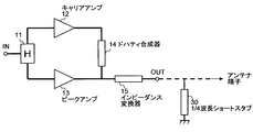
- FIG. 1 shows an equivalent circuit of a Doherty amplifier according to this embodiment.
- the Doherty amplifier of this embodiment includes a signal distributor (Hybrid) 11, a carrier amplifier 12, a peak amplifier 13, a Doherty synthesizer 14, and an impedance converter 15. Yes.
- the carrier amplifier 12 corresponds to the first amplifier
- the peak amplifier 13 corresponds to the second amplifier.
- the signal distributor 11 distributes the signal input via the input terminal IN to the carrier amplifier 12 and the peak amplifier 13 and outputs the result.
- the signal distributor 11 outputs a signal delayed by 90 ° to the peak amplifier 13 side.
- the carrier amplifier 12 is a class AB amplifier that always amplifies one of the signals distributed by the signal distributor 11.
- the peak amplifier 13 is a class C amplifier that amplifies only a signal having a predetermined level or higher among the other signals distributed by the signal distributor 11.
- the Doherty synthesizer 14 is connected to the output of the carrier amplifier 12 and the output of the peak amplifier 13 and is provided to synthesize the output signal of the carrier amplifier 12 with the output signal of the peak amplifier 13.
- the impedance converter 15 is connected to the output of the peak amplifier 13 and the output terminal OUT, and is provided for impedance conversion of the characteristic impedance Z 0 ⁇ ⁇ 1/2 ⁇ Z 0 .
- the characteristic impedance Z 0 of each of the Doherty combiner 14 and the impedance converter 15 is determined from a desired impedance conversion ratio according to the configuration of the Doherty amplifier.
- the Doherty combiner 14 the characteristic impedance Z 0 of the is set to 50 [Omega, the characteristic impedance Z 0 of the impedance converter is set to 35 ⁇ ( ⁇ ⁇ (50 * 25 )).
- the Doherty synthesizer 14 and the impedance converter 15 are basically composed of a transmission line of 1 ⁇ 4 wavelength.
- this configuration occupies a certain mounting area (volume), which is disadvantageous for miniaturization.
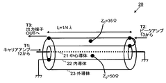
- the Doherty synthesizer 14 and the impedance converter 15 are realized by the transmission line transformer 20 having a quarter-wavelength double coaxial structure. Miniaturize.
- T1 to T3 correspond to the positions of T1 to T3 in FIG.
- the transmission line transformer 20 has an axial length L of 1 ⁇ 4 wavelength, and a center conductor 21, an inner conductor 22, and an outer conductor 23 are formed in this order from the center toward the outside. It has a double coaxial structure. A dielectric is filled between the center conductor 21 and the inner conductor 22 and between the inner conductor 22 and the outer conductor 23.
- central conductor 21 and the inner conductor 22 constitute a first coaxial line
- the inner conductor 22 and the outer conductor 23 constitute a second coaxial line.
- the output of the carrier amplifier 12 is connected to one end (the left end in FIG. 2) of the first coaxial line, and the output terminal OUT is connected to one end (the left end in FIG. 2) of the second coaxial line.
- the other end of the line (right end in FIG. 2), the output of the peak amplifier 13 and the other end of the second coaxial line (right end in FIG. 2) are connected.
- the center conductor 21 is connected to the output of the carrier amplifier 12, the inner conductor 22 is grounded, and the outer conductor 23 is connected to the output terminal OUT. It is connected to the. Further, at the other end of the first and second coaxial lines (the right end in FIG. 2), the center conductor 21 is grounded, the inner conductor 22 and the outer conductor 23 are connected, and the outer conductor 23 serves as the output of the peak amplifier 13. It is connected.
- the characteristic impedance Z 0 of the first coaxial line is set to 50 [Omega, the characteristic impedance Z 0 of the second coaxial line is set to 35 ⁇ .
- the Doherty combiner 14 can be realized by the first coaxial line, and the impedance converter 15 can be realized by the second coaxial line.
- each of the Doherty synthesizer 14 and the impedance converter 15 requires a mounting area (volume), whereas in the Doherty amplifier of this embodiment, the Doherty synthesizer 14 and the impedance converter
- the vessel 15 can share a part of the conductor (inner conductor 22).
- the Doherty amplifier itself can be reduced in size and weight, a transmitter using the Doherty amplifier can be reduced in size.
- the characteristic impedance Z 0 of the first coaxial line and the second coaxial line can be changed by appropriately changing the dielectric constant of the dielectric filled therein and the radius of the coaxial line. It can be set to the above values.
- the output signal of the carrier amplifier 12 is further inverted in sign in addition to the phase delay of 90 ° (for 1 ⁇ 4 wavelength) generated by propagating through the Doherty combiner 14.
- a phase delay of 180 ° occurs (phase inversion type).
- the signal distributor 11 further delays the phase of the signal output to the peak amplifier 13 side by 180 °. Thereby, the output signals of the carrier amplifier 12 and the peak amplifier 13 can be synthesized in phase at the synthesis point.
- a 1/4 wavelength short circuit occurs in the signal path between the transmission amplifier and the antenna terminal due to the role of a surge absorber. Stubs and coils are provided.
- the base station shown in FIG. 3 uses a Doherty amplifier as a transmission amplifier, and a 1/4 wavelength short stub in the signal path between the output terminal OUT and the antenna terminal of the Doherty amplifier serves as a surge absorber. 30 is provided.
- the Doherty amplifier of this embodiment when viewed from the output terminal OUT, the output of the carrier amplifier 12 is grounded at the other end (the right end in FIG. 2) of the transmission line transformer 20 via the center conductor 21.
- the output of the peak amplifier 13 is grounded at one end (the left end in FIG. 2) of the transmission line transformer 20 via the inner conductor 22.
- the Doherty amplifier according to the present embodiment has a surge absorber function that releases the surge current flowing from the antenna terminal.
- a configuration without a surge absorber can also be provided, and this configuration can contribute to downsizing and cost reduction of the base station.
- the Doherty amplifier according to the present embodiment is applied to a base station provided with a surge absorber, it is possible to further improve the proof strength against a surge current from the antenna terminal. As a result, it is possible to contribute to the improvement of the reliability of the base station, and it is possible to reduce the required tolerance for the surge absorber, thereby contributing to the cost reduction of the base station and the simplification of the internal circuit. .
- the Doherty amplifier of the present embodiment is different from the first embodiment in the connection configuration of the other end (right end of FIG. 2) of the transmission line transformer 20, and the others are the same. .
- FIG. 4 shows the configuration of the transmission line transformer 20 used in the Doherty amplifier of this embodiment.
- T1 to T3 correspond to the positions of T1 to T3 in FIG.
- the central conductor 21 is connected to the carrier amplifier 12 at one end of the first and second coaxial lines (the left end of FIG. 4) as in the first embodiment.
- the inner conductor 22 is grounded, and the outer conductor 23 is connected to the output terminal OUT.
- the inner conductor 22 is grounded, the center conductor 21 and the outer conductor 23 are connected, and the center conductor 21 serves as the output of the peak amplifier 13. It is connected.
- the output signal of the carrier amplifier 12 has only a phase delay of 90 ° (for 1 ⁇ 4 wavelength) generated by propagating through the Doherty synthesizer 14 (phase non-inversion type).
- FIG. 5 shows an equivalent circuit of the Doherty amplifier of this embodiment.
- the Doherty amplifier of this embodiment has the same circuit configuration as that of the first and second embodiments.
- the Doherty combiner 14 is realized by the first coaxial line constituted by the center conductor 21 and the inner conductor 22, and the inner conductor 22 and the outer conductor 23 are
- the impedance converter 15 is realized by the second coaxial line configured as follows.
- the impedance converter 15 is realized by the first coaxial line
- the Doherty combiner 14 is realized by the second coaxial line.
- FIG. 6 shows the configuration of the transmission line transformer 20 used in the Doherty amplifier of this embodiment.
- T1 to T3 correspond to the positions of T1 to T3 in FIG.
- the output terminal OUT is connected to one end (the left end in FIG. 6) of the first coaxial line composed of the center conductor 21 and the inner conductor 22.
- the output of the carrier amplifier 12 is connected to one end (left end in FIG. 6) of the second coaxial line composed of the conductor 22 and the outer conductor 23, and the other end (right end in FIG. 6) of the first coaxial line;
- the output of the peak amplifier 13 is connected to the other end of the second coaxial line (the right end in FIG. 6).
- the center conductor 21 is connected to the output terminal OUT, the inner conductor 22 is grounded, and the outer conductor 23 is the output of the carrier amplifier 12. It is connected to the.
- the center conductor 21 is grounded, the inner conductor 22 and the outer conductor 23 are connected, and the outer conductor 23 serves as the output of the peak amplifier 13. It is connected.
- the impedance converter 15 is realized by the first coaxial line, and the characteristic impedance of the first coaxial line is realized by realizing the Doherty combiner 14 by the second coaxial line.
- Z 0 is set to 35 ⁇ , and the characteristic impedance Z 0 of the second coaxial line is set to 50 ⁇ .
- the Doherty amplifier 14 and the impedance converter 15 can share a part of the conductor (inner conductor 22) as in the first and second embodiments. It is possible to reduce the size and weight of the transmitter itself, thereby reducing the size of the transmitter using the Doherty amplifier.
- the output signal of the carrier amplifier 12 has a phase of 90 ° (for 1 ⁇ 4 wavelength) generated by propagating through the Doherty combiner 14 as in the first embodiment.
- the sign is further reversed, resulting in a phase delay of 180 ° (phase inversion type).
- the signal distributor 11 further delays the phase of the signal output to the peak amplifier 13 side by 180 °. Thereby, the output signals of the carrier amplifier 12 and the peak amplifier 13 can be synthesized in phase at the synthesis point.
- the outputs of the carrier amplifier 12 and the peak amplifier 13 are both grounded at one end of the transmission line transformer 20 (the left end in FIG. 6) via the inner conductor 22. ing.
- the Doherty amplifier of the present embodiment has a surge absorber function that releases the surge current flowing from the antenna terminal, as in the first embodiment.
- a configuration without a surge absorber can also be provided, and this configuration can contribute to downsizing and cost reduction of the base station.
- the Doherty amplifier according to the present embodiment is applied to a base station provided with a surge absorber, it is possible to further improve the proof strength against a surge current from the antenna terminal. As a result, it is possible to contribute to the improvement of the reliability of the base station, and it is possible to reduce the required tolerance for the surge absorber, thereby contributing to the cost reduction of the base station and the simplification of the internal circuit. .
- the Doherty amplifier of this embodiment is different from the third embodiment in the connection configuration of the other end (the right end in FIG. 6) of the transmission line transformer 20, and the others are the same. .
- FIG. 7 shows the configuration of the transmission line transformer 20 used in the Doherty amplifier of this embodiment.
- T1 to T3 correspond to the positions of T1 to T3 in FIG.
- the central conductor 21 is connected to the output terminal OUT at one end of the first and second coaxial lines (the left end of FIG. 7), as in the third embodiment.
- the inner conductor 22 is grounded, and the outer conductor 23 is connected to the output of the carrier amplifier 12. Further, at the other ends (right ends in FIG. 7) of the first and second coaxial lines, the inner conductor 22 is grounded, the center conductor 21 and the outer conductor 23 are connected, and the center conductor 21 serves as the output of the peak amplifier 13. It is connected.
- the output signal of the carrier amplifier 12 has only a phase delay of 90 ° (for 1 ⁇ 4 wavelength) generated by propagating through the Doherty combiner 14 as in the second embodiment. Occurs (phase non-inversion type).
- the signal distributor 11 may delay the phase of the signal output to the peak amplifier 13 side by 90 °.
- the transmission amplifier of the present invention is applied to a Doherty amplifier.
- the present invention can also be applied to an amplifier called a Doherty amplifier.
- the peak amplifier 13 corresponds to the first amplifier
- the carrier amplifier 12 corresponds to the second amplifier.
- transmission line transformer 20 in the case where the present invention is applied to the inverted Doherty amplifier can have the four configurations described in the first to fourth embodiments.
- the transmission line transformer 20 which has a double coaxial structure was used, as shown in FIG. 9, this invention does not have the impedance converter 15 as a phase inversion type double coaxial structure.
- a quarter-wave transmission line transformer (a coaxial structure in which a center conductor and an outer conductor are formed in this order from the center toward the outside) may be used. In this configuration, at one end of the transmission line transformer (left end in FIG. 9), the center conductor is connected to the output of the peak amplifier 13 and the outer conductor is grounded. Further, at the other end of the transmission line transformer (the right end in FIG. 9), the center conductor is grounded and the outer conductor is connected to the output terminal OUT.
- the Doherty amplifier of FIG. 9 has a surge absorber function. Become. Therefore, when the Doherty amplifier of FIG. 9 is applied to a transmitter, a configuration without a surge absorber can be provided, and the transmitter can be reduced in size and cost. In this configuration, since the phase is inverted after the output signals of the carrier amplifier 12 and the peak amplifier 13 are combined, the signal distributor 11 does not need to further delay the phase of the signal output to the peak amplifier 13 side by 180 °. .
- the Doherty combiner 14 is also a phase-inverted 1/4 wavelength transmission line transformer (a coaxial structure in which a center conductor and an outer conductor are formed in this order from the center toward the outside. Yes).
- the central conductor is connected to the output of the carrier amplifier 12 and the outer conductor is grounded at one end (the upper end in FIG. 9) of the transmission line transformer. Further, at the other end of this transmission line transformer (lower end in FIG. 9), the center conductor is grounded, and the outer conductor is connected to the output of the peak amplifier 13.
- the signal distributor 11 needs to further delay the phase of the signal output to the peak amplifier 13 side by 180 °. is there.
- both the Doherty synthesizer 14 and the impedance converter 15 are formed of phase-inverted quarter-wavelength transmission line transformers, they can be formed as a single unit.
- the transmission line transformer 20 having the double coaxial structure used is obtained.
- FIG. 9 is applicable not only to the Doherty amplifier but also to the inverted Doherty amplifier.
- the transmission line transformer has a coaxial structure.
- a transmission line transformer composed of a planar circuit such as a printed circuit board can be used, for example.
- the transmission line transformer only needs to have a pair of conductors.
- an equivalent phase inversion type 1 can be obtained by appropriately selecting a combination of connection / grounding of the center conductor and the outer conductor at one end (left end in FIG. 9) and the other end (right end in FIG. 9) of the transmission line transformer. It will be apparent to those skilled in the art that a / 4 wavelength transmission line transformer is obtained.
Landscapes
- Engineering & Computer Science (AREA)
- Power Engineering (AREA)
- Microelectronics & Electronic Packaging (AREA)
- Computer Networks & Wireless Communication (AREA)
- Signal Processing (AREA)
- Amplifiers (AREA)
- Microwave Amplifiers (AREA)
Description
キャリアアンプおよびピークアンプの一方を第1のアンプとして有すると共に、他方を第2のアンプとして有する送信増幅器であって、
中心から外側に向けて、中心導体と、内導体と、外導体と、がこの順に形成された、1/4波長の2重同軸構造を有する伝送線路トランスを有し、
前記中心導体と前記内導体とで第1の同軸線路が構成され、
前記内導体と前記外導体とで第2の同軸線路が構成され、
前記第1および第2の同軸線路の一方の一端に前記第1のアンプの出力が接続され、
前記第1および第2の同軸線路の他方の一端に出力端子が接続され、
前記第1の同軸線路の他端と、前記第2のアンプの出力と、前記第2の同軸線路の他端と、が接続されることを特徴とする。
キャリアアンプおよびピークアンプの一方を第1のアンプとして有すると共に、他方を第2のアンプとして有する送信増幅器であって、
前記第1のアンプの出力と前記第2のアンプの出力とに接続される1/4波長の第1の伝送線路トランスと、
前記第2のアンプの出力と出力端子とに接続される1/4波長の第2の伝送線路トランスと、を有し、
前記第2の伝送線路トランスは、対となる導体を有しており、
前記第2の伝送線路トランスの一端において、前記対となる導体のうち一方の導体が前記第2のアンプの出力に接続され、前記対となる導体のうち他方の導体が接地され、
前記第2の伝送線路トランスの他端において、前記対となる導体のうち前記一方の導体が接地され、前記対となる導体のうち前記他方の導体が前記出力端子に接続される。
前記送信増幅器を用いることを特徴とする。
(1)第1の実施形態
図1に、本実施形態のドハティ増幅器の等価回路を示す。
(2)第2の実施形態
本実施形態のドハティ増幅器は、第1の実施形態と比較して、伝送線路トランス20の他端(図2の右端)の接続構成が異なり、その他は同様である。
(3)第3の実施形態
図5に、本実施形態のドハティ増幅器の等価回路を示す。
(4)第4の実施形態
本実施形態のドハティ増幅器は、第3の実施形態と比較して、伝送線路トランス20の他端(図6の右端)の接続構成が異なり、その他は同様である。
Claims (15)
- キャリアアンプおよびピークアンプの一方を第1のアンプとして有すると共に、他方を第2のアンプとして有する送信増幅器であって、
中心から外側に向けて、中心導体と、内導体と、外導体と、がこの順に形成された、1/4波長の2重同軸構造を有する伝送線路トランスを有し、
前記中心導体と前記内導体とで第1の同軸線路が構成され、
前記内導体と前記外導体とで第2の同軸線路が構成され、
前記第1および第2の同軸線路の一方の一端に前記第1のアンプの出力が接続され、
前記第1および第2の同軸線路の他方の一端に出力端子が接続され、
前記第1の同軸線路の他端と、前記第2のアンプの出力と、前記第2の同軸線路の他端と、が接続される、送信増幅器。 - 前記第1の同軸線路の一端に前記第1のアンプの出力が接続され、
前記第2の同軸線路の一端に前記出力端子が接続される、請求項1に記載の送信増幅器。 - 前記第1および第2の同軸線路の一端において、前記中心導体が前記第1のアンプの出力に接続され、前記内導体が接地され、前記外導体が前記出力端子に接続され、
前記第1および第2の同軸線路の他端において、前記中心導体が接地され、前記内導体と前記外導体とが接続され、前記外導体が前記第2のアンプの出力に接続される、請求項2に記載の送信増幅器。 - 前記第1および第2の同軸線路の一端において、前記中心導体が前記第1のアンプの出力に接続され、前記内導体が接地され、前記外導体が前記出力端子に接続され、
前記第1および第2の同軸線路の他端において、前記内導体が接地され、前記中心導体と前記外導体とが接続され、前記中心導体が前記第2のアンプの出力に接続される、請求項2に記載の送信増幅器。 - 前記第1の同軸線路の一端に前記出力端子が接続され、
前記第2の同軸線路の一端に前記第1のアンプの出力が接続される、請求項1に記載の送信増幅器。 - 前記第1および第2の同軸線路の一端において、前記中心導体が前記出力端子に接続され、前記内導体が接地され、前記外導体が前記第1のアンプの出力に接続され、
前記第1および第2の同軸線路の他端において、前記中心導体が接地され、前記内導体と前記外導体とが接続され、前記外導体が前記第2のアンプの出力に接続される、請求項5に記載の送信増幅器。 - 前記第1および第2の同軸線路の一端において、前記中心導体が前記出力端子に接続され、前記内導体が接地され、前記外導体が前記第1のアンプの出力に接続され、
前記第1および第2の同軸線路の他端において、前記内導体が接地され、前記中心導体と前記外導体とが接続され、前記中心導体が前記第2のアンプの出力に接続される、請求項5に記載の送信増幅器。 - キャリアアンプおよびピークアンプの一方を第1のアンプとして有すると共に、他方を第2のアンプとして有する送信増幅器であって、
前記第1のアンプの出力と前記第2のアンプの出力とに接続される1/4波長の第1の伝送線路トランスと、
前記第2のアンプの出力と出力端子とに接続される1/4波長の第2の伝送線路トランスと、を有し、
前記第2の伝送線路トランスは、対となる導体を有しており、
前記第2の伝送線路トランスの一端において、前記対となる導体のうち一方の導体が前記第2のアンプの出力に接続され、前記対となる導体のうち他方の導体が接地され、
前記第2の伝送線路トランスの他端において、前記対となる導体のうち前記一方の導体が接地され、前記対となる導体のうち前記他方の導体が前記出力端子に接続される、送信増幅器。 - 前記第2の伝送線路トランスは、
中心から外側に向けて、中心導体と、外導体と、がこの順に形成された、1/4波長の同軸構造を有する伝送線路トランスであり、
前記第2の伝送線路トランスの一端において、前記中心導体が前記第2のアンプの出力に接続され、前記外導体が接地され、
前記第2の伝送線路トランスの他端において、前記中心導体が接地され、前記外導体が前記出力端子に接続される、請求項8に記載の送信増幅器。 - 前記第2の伝送線路トランスは、
中心から外側に向けて、中心導体と、外導体と、がこの順に形成された、1/4波長の同軸構造を有する伝送線路トランスであり、
前記第2の伝送線路トランスの一端において、前記外導体が前記第2のアンプの出力に接続され、前記中心導体が接地され、
前記第2の伝送線路トランスの他端において、前記外導体が接地され、前記中心導体が前記出力端子に接続される、請求項8に記載の送信増幅器。 - 前記第1の伝送線路トランスは、
中心から外側に向けて、中心導体と、外導体と、がこの順に形成された、1/4波長の同軸構造を有する伝送線路トランスであり、
前記第1の伝送線路トランスの一端において、前記中心導体が前記第1のアンプの出力に接続され、前記外導体が接地され、
前記第1の伝送線路トランスの他端において、前記中心導体が接地され、前記外導体が前記第2のアンプの出力に接続される、請求項8から10のいずれか1項に記載の送信増幅器。 - 前記第1の伝送線路トランスは、
中心から外側に向けて、中心導体と、外導体と、がこの順に形成された、1/4波長の同軸構造を有する伝送線路トランスであり、
前記第1の伝送線路トランスの一端において、前記外導体が前記第1のアンプの出力に接続され、前記中心導体が接地され、
前記第1の伝送線路トランスの他端において、前記外導体が接地され、前記中心導体が前記第2のアンプの出力に接続される、請求項8から10のいずれか1項に記載の送信増幅器。 - 前記第1のアンプは、前記キャリアアンプであり、
前記第2のアンプは、前記ピークアンプである、請求項1から12のいずれか1項に記載の送信増幅器。 - 前記第1のアンプは、前記ピークアンプであり、
前記第2のアンプは、前記キャリアアンプである、請求項1から12のいずれか1項に記載の送信増幅器。 - 請求項1から14のいずれか1項に記載の送信増幅器を用いる送信機。
Priority Applications (2)
| Application Number | Priority Date | Filing Date | Title |
|---|---|---|---|
| US14/427,262 US9503029B2 (en) | 2012-09-14 | 2013-04-09 | Transmitting amplifier and transmitter |
| JP2014535389A JP5831642B2 (ja) | 2012-09-14 | 2013-04-09 | 送信増幅器、送信機 |
Applications Claiming Priority (2)
| Application Number | Priority Date | Filing Date | Title |
|---|---|---|---|
| JP2012-202590 | 2012-09-14 | ||
| JP2012202590 | 2012-09-14 |
Publications (1)
| Publication Number | Publication Date |
|---|---|
| WO2014041835A1 true WO2014041835A1 (ja) | 2014-03-20 |
Family
ID=50277973
Family Applications (1)
| Application Number | Title | Priority Date | Filing Date |
|---|---|---|---|
| PCT/JP2013/060697 Ceased WO2014041835A1 (ja) | 2012-09-14 | 2013-04-09 | 送信増幅器、送信機 |
Country Status (3)
| Country | Link |
|---|---|
| US (1) | US9503029B2 (ja) |
| JP (1) | JP5831642B2 (ja) |
| WO (1) | WO2014041835A1 (ja) |
Families Citing this family (4)
| Publication number | Priority date | Publication date | Assignee | Title |
|---|---|---|---|---|
| US11108360B2 (en) * | 2018-07-20 | 2021-08-31 | Qorvo Us, Inc. | Doherty power amplifier system |
| DE102019000324A1 (de) * | 2019-01-20 | 2020-07-23 | IAD Gesellschaft für Informatik, Automatisierung und Datenverarbeitung mbH | Sende- und Empfangsvorrichtung mit einem Breitband HF-Leistungsverstärker, insbesondere N-Wege-Doherty Verstärker mit aktiver Lastmodulation |
| US11201593B2 (en) | 2019-12-11 | 2021-12-14 | Qorvo Us, Inc. | Doherty power amplifier system |
| US20230088601A1 (en) * | 2021-09-15 | 2023-03-23 | Samsung Electronics Co., Ltd. | Method for processing incomplete continuous utterance and server and electronic device for performing the method |
Citations (4)
| Publication number | Priority date | Publication date | Assignee | Title |
|---|---|---|---|---|
| JPH1168420A (ja) * | 1997-08-12 | 1999-03-09 | Mitsubishi Electric Corp | バラン及びプッシュプル増幅器 |
| JP2001127650A (ja) * | 1999-10-26 | 2001-05-11 | Nippon Soken Inc | 通信装置 |
| JP2006067176A (ja) * | 2004-08-26 | 2006-03-09 | Nec Corp | ドハティ増幅器並列運転回路 |
| JP2006148780A (ja) * | 2004-11-24 | 2006-06-08 | Matsushita Electric Ind Co Ltd | 高周波ドハティ増幅器 |
Family Cites Families (2)
| Publication number | Priority date | Publication date | Assignee | Title |
|---|---|---|---|---|
| US3504306A (en) * | 1969-06-02 | 1970-03-31 | Sylvania Electric Prod | Triaxial balun for broadband push-pull power amplifier |
| JP2010206351A (ja) | 2009-03-02 | 2010-09-16 | Hitachi Kokusai Electric Inc | 電力検出器 |
-
2013
- 2013-04-09 JP JP2014535389A patent/JP5831642B2/ja not_active Expired - Fee Related
- 2013-04-09 WO PCT/JP2013/060697 patent/WO2014041835A1/ja not_active Ceased
- 2013-04-09 US US14/427,262 patent/US9503029B2/en not_active Expired - Fee Related
Patent Citations (4)
| Publication number | Priority date | Publication date | Assignee | Title |
|---|---|---|---|---|
| JPH1168420A (ja) * | 1997-08-12 | 1999-03-09 | Mitsubishi Electric Corp | バラン及びプッシュプル増幅器 |
| JP2001127650A (ja) * | 1999-10-26 | 2001-05-11 | Nippon Soken Inc | 通信装置 |
| JP2006067176A (ja) * | 2004-08-26 | 2006-03-09 | Nec Corp | ドハティ増幅器並列運転回路 |
| JP2006148780A (ja) * | 2004-11-24 | 2006-06-08 | Matsushita Electric Ind Co Ltd | 高周波ドハティ増幅器 |
Also Published As
| Publication number | Publication date |
|---|---|
| JP5831642B2 (ja) | 2015-12-09 |
| US9503029B2 (en) | 2016-11-22 |
| US20150229276A1 (en) | 2015-08-13 |
| JPWO2014041835A1 (ja) | 2016-08-18 |
Similar Documents
| Publication | Publication Date | Title |
|---|---|---|
| US9899962B2 (en) | Power amplifier | |
| JP4715994B2 (ja) | ドハティ増幅器並列運転回路 | |
| EP3461000B1 (en) | Doherty amplifier | |
| US20190165738A1 (en) | Wideband power combiner and splitter | |
| JP2014523717A (ja) | 広帯域変換器を用いた広帯域ドハティ増幅器 | |
| JP5831642B2 (ja) | 送信増幅器、送信機 | |
| CN108111129B (zh) | 功率放大器 | |
| JP6176333B2 (ja) | 電力増幅器及び電力増幅方法 | |
| US11398798B2 (en) | Doherty power amplifiers with coupled line combiners | |
| US9929465B2 (en) | Antenna array and phased array system to which antenna array is applied | |
| JP5035846B2 (ja) | ドハティ増幅回路 | |
| CN114915266A (zh) | 射频放大电路和射频前端模组 | |
| WO2024188077A1 (zh) | 功率放大器芯片、模组、电路、射频前端模组及通信设备 | |
| JP5787123B2 (ja) | 方向性結合器および無線通信装置 | |
| JPWO2012002407A1 (ja) | 高周波電力増幅器 | |
| KR20240050197A (ko) | 도허티 전력 증폭기 및 이를 포함하는 전자 장치 | |
| JP5694876B2 (ja) | アンテナ装置および無線通信システム | |
| TWI271043B (en) | High power parallel block-up converter | |
| CN111064481A (zh) | 一种信号处理装置及设备 | |
| JP6645333B2 (ja) | ドハティ増幅器 | |
| JP2014057207A (ja) | 方向性結合器および無線通信装置 | |
| JP2012080397A (ja) | 逆相分配回路及びアンテナ装置 | |
| US20220416751A1 (en) | Impedance matching circuit and an impedance matching element | |
| WO2024157642A1 (ja) | 増幅回路および通信装置 | |
| EP4544675A1 (en) | Dual-band dual-output ports power amplifier arrangements |
Legal Events
| Date | Code | Title | Description |
|---|---|---|---|
| 121 | Ep: the epo has been informed by wipo that ep was designated in this application |
Ref document number: 13836666 Country of ref document: EP Kind code of ref document: A1 |
|
| ENP | Entry into the national phase |
Ref document number: 2014535389 Country of ref document: JP Kind code of ref document: A |
|
| WWE | Wipo information: entry into national phase |
Ref document number: 14427262 Country of ref document: US |
|
| NENP | Non-entry into the national phase |
Ref country code: DE |
|
| 122 | Ep: pct application non-entry in european phase |
Ref document number: 13836666 Country of ref document: EP Kind code of ref document: A1 |