WO2014038180A1 - 電源装置および管理装置 - Google Patents
電源装置および管理装置 Download PDFInfo
- Publication number
- WO2014038180A1 WO2014038180A1 PCT/JP2013/005192 JP2013005192W WO2014038180A1 WO 2014038180 A1 WO2014038180 A1 WO 2014038180A1 JP 2013005192 W JP2013005192 W JP 2013005192W WO 2014038180 A1 WO2014038180 A1 WO 2014038180A1
- Authority
- WO
- WIPO (PCT)
- Prior art keywords
- battery cells
- cell management
- battery
- voltage
- asic
- Prior art date
- Legal status (The legal status is an assumption and is not a legal conclusion. Google has not performed a legal analysis and makes no representation as to the accuracy of the status listed.)
- Ceased
Links
Images

Classifications
-
- H—ELECTRICITY
- H02—GENERATION; CONVERSION OR DISTRIBUTION OF ELECTRIC POWER
- H02J—ELECTRIC POWER NETWORKS; CIRCUIT ARRANGEMENTS OR SYSTEMS FOR SUPPLYING OR DISTRIBUTING ELECTRIC POWER; SYSTEMS FOR STORING ELECTRIC ENERGY
- H02J7/00—Circuit arrangements for charging or discharging batteries or for supplying loads from batteries
- H02J7/50—Circuit arrangements for charging or discharging batteries or for supplying loads from batteries acting upon multiple batteries simultaneously or sequentially
- H02J7/52—Circuit arrangements for charging or discharging batteries or for supplying loads from batteries acting upon multiple batteries simultaneously or sequentially for charge balancing, e.g. equalisation of charge between batteries
-
- B—PERFORMING OPERATIONS; TRANSPORTING
- B60—VEHICLES IN GENERAL
- B60L—PROPULSION OF ELECTRICALLY-PROPELLED VEHICLES; SUPPLYING ELECTRIC POWER FOR AUXILIARY EQUIPMENT OF ELECTRICALLY-PROPELLED VEHICLES; ELECTRODYNAMIC BRAKE SYSTEMS FOR VEHICLES IN GENERAL; MAGNETIC SUSPENSION OR LEVITATION FOR VEHICLES; MONITORING OPERATING VARIABLES OF ELECTRICALLY-PROPELLED VEHICLES; ELECTRIC SAFETY DEVICES FOR ELECTRICALLY-PROPELLED VEHICLES
- B60L58/00—Methods or circuit arrangements for monitoring or controlling batteries or fuel cells, specially adapted for electric vehicles
- B60L58/10—Methods or circuit arrangements for monitoring or controlling batteries or fuel cells, specially adapted for electric vehicles for monitoring or controlling batteries
- B60L58/18—Methods or circuit arrangements for monitoring or controlling batteries or fuel cells, specially adapted for electric vehicles for monitoring or controlling batteries of two or more battery modules
- B60L58/22—Balancing the charge of battery modules
-
- H—ELECTRICITY
- H01—ELECTRIC ELEMENTS
- H01M—PROCESSES OR MEANS, e.g. BATTERIES, FOR THE DIRECT CONVERSION OF CHEMICAL ENERGY INTO ELECTRICAL ENERGY
- H01M10/00—Secondary cells; Manufacture thereof
- H01M10/42—Methods or arrangements for servicing or maintenance of secondary cells or secondary half-cells
- H01M10/425—Structural combination with electronic components, e.g. electronic circuits integrated to the outside of the casing
- H01M10/4257—Smart batteries, e.g. electronic circuits inside the housing of the cells or batteries
-
- H—ELECTRICITY
- H01—ELECTRIC ELEMENTS
- H01M—PROCESSES OR MEANS, e.g. BATTERIES, FOR THE DIRECT CONVERSION OF CHEMICAL ENERGY INTO ELECTRICAL ENERGY
- H01M10/00—Secondary cells; Manufacture thereof
- H01M10/42—Methods or arrangements for servicing or maintenance of secondary cells or secondary half-cells
- H01M10/48—Accumulators combined with arrangements for measuring, testing or indicating the condition of cells, e.g. the level or density of the electrolyte
- H01M10/482—Accumulators combined with arrangements for measuring, testing or indicating the condition of cells, e.g. the level or density of the electrolyte for several batteries or cells simultaneously or sequentially
-
- B—PERFORMING OPERATIONS; TRANSPORTING
- B60—VEHICLES IN GENERAL
- B60L—PROPULSION OF ELECTRICALLY-PROPELLED VEHICLES; SUPPLYING ELECTRIC POWER FOR AUXILIARY EQUIPMENT OF ELECTRICALLY-PROPELLED VEHICLES; ELECTRODYNAMIC BRAKE SYSTEMS FOR VEHICLES IN GENERAL; MAGNETIC SUSPENSION OR LEVITATION FOR VEHICLES; MONITORING OPERATING VARIABLES OF ELECTRICALLY-PROPELLED VEHICLES; ELECTRIC SAFETY DEVICES FOR ELECTRICALLY-PROPELLED VEHICLES
- B60L2240/00—Control parameters of input or output; Target parameters
- B60L2240/40—Drive Train control parameters
- B60L2240/54—Drive Train control parameters related to batteries
- B60L2240/547—Voltage
-
- B—PERFORMING OPERATIONS; TRANSPORTING
- B60—VEHICLES IN GENERAL
- B60L—PROPULSION OF ELECTRICALLY-PROPELLED VEHICLES; SUPPLYING ELECTRIC POWER FOR AUXILIARY EQUIPMENT OF ELECTRICALLY-PROPELLED VEHICLES; ELECTRODYNAMIC BRAKE SYSTEMS FOR VEHICLES IN GENERAL; MAGNETIC SUSPENSION OR LEVITATION FOR VEHICLES; MONITORING OPERATING VARIABLES OF ELECTRICALLY-PROPELLED VEHICLES; ELECTRIC SAFETY DEVICES FOR ELECTRICALLY-PROPELLED VEHICLES
- B60L2240/00—Control parameters of input or output; Target parameters
- B60L2240/40—Drive Train control parameters
- B60L2240/54—Drive Train control parameters related to batteries
- B60L2240/549—Current
-
- H—ELECTRICITY
- H01—ELECTRIC ELEMENTS
- H01M—PROCESSES OR MEANS, e.g. BATTERIES, FOR THE DIRECT CONVERSION OF CHEMICAL ENERGY INTO ELECTRICAL ENERGY
- H01M2220/00—Batteries for particular applications
- H01M2220/20—Batteries in motive systems, e.g. vehicle, ship, plane
-
- Y—GENERAL TAGGING OF NEW TECHNOLOGICAL DEVELOPMENTS; GENERAL TAGGING OF CROSS-SECTIONAL TECHNOLOGIES SPANNING OVER SEVERAL SECTIONS OF THE IPC; TECHNICAL SUBJECTS COVERED BY FORMER USPC CROSS-REFERENCE ART COLLECTIONS [XRACs] AND DIGESTS
- Y02—TECHNOLOGIES OR APPLICATIONS FOR MITIGATION OR ADAPTATION AGAINST CLIMATE CHANGE
- Y02E—REDUCTION OF GREENHOUSE GAS [GHG] EMISSIONS, RELATED TO ENERGY GENERATION, TRANSMISSION OR DISTRIBUTION
- Y02E60/00—Enabling technologies; Technologies with a potential or indirect contribution to GHG emissions mitigation
- Y02E60/10—Energy storage using batteries
-
- Y—GENERAL TAGGING OF NEW TECHNOLOGICAL DEVELOPMENTS; GENERAL TAGGING OF CROSS-SECTIONAL TECHNOLOGIES SPANNING OVER SEVERAL SECTIONS OF THE IPC; TECHNICAL SUBJECTS COVERED BY FORMER USPC CROSS-REFERENCE ART COLLECTIONS [XRACs] AND DIGESTS
- Y02—TECHNOLOGIES OR APPLICATIONS FOR MITIGATION OR ADAPTATION AGAINST CLIMATE CHANGE
- Y02T—CLIMATE CHANGE MITIGATION TECHNOLOGIES RELATED TO TRANSPORTATION
- Y02T10/00—Road transport of goods or passengers
- Y02T10/60—Other road transportation technologies with climate change mitigation effect
- Y02T10/70—Energy storage systems for electromobility, e.g. batteries
-
- Y—GENERAL TAGGING OF NEW TECHNOLOGICAL DEVELOPMENTS; GENERAL TAGGING OF CROSS-SECTIONAL TECHNOLOGIES SPANNING OVER SEVERAL SECTIONS OF THE IPC; TECHNICAL SUBJECTS COVERED BY FORMER USPC CROSS-REFERENCE ART COLLECTIONS [XRACs] AND DIGESTS
- Y02—TECHNOLOGIES OR APPLICATIONS FOR MITIGATION OR ADAPTATION AGAINST CLIMATE CHANGE
- Y02T—CLIMATE CHANGE MITIGATION TECHNOLOGIES RELATED TO TRANSPORTATION
- Y02T90/00—Enabling technologies or technologies with a potential or indirect contribution to GHG emissions mitigation
- Y02T90/10—Technologies relating to charging of electric vehicles
- Y02T90/16—Information or communication technologies improving the operation of electric vehicles
Definitions
- the present invention relates to a power supply device including an assembled battery in which a plurality of battery cells are connected in series, and a management device for managing the plurality of battery cells.
- HV hybrid vehicles
- PSV plug-in hybrid vehicles
- EV electric vehicles
- lithium ion batteries are close to the regular use area and the prohibited use area, stricter voltage management is required than other types of batteries.
- a voltage detection circuit for detecting the voltage of each battery cell is provided. The detected voltage of each battery cell is used for charge / discharge control, cell voltage equalization control, and the like.
- a secondary battery for vehicle use requires a high output voltage, it is often used by connecting a plurality of assembled batteries in series.
- a configuration in which a plurality of IC chips each mounted with a voltage detection circuit are connected in cascade with a plurality of assembled batteries.
- a voltage exceeding the withstand voltage may be applied to a specific IC chip. is there. This overvoltage can also occur during maintenance of the power supply device. This overvoltage can be suppressed if the IC chip is designed to have a high withstand voltage, but this leads to an increase in cost.
- the present invention has been made in view of such circumstances, and an object of the present invention is to provide a technique that suppresses over-withstand pressure at the time of assembly and maintenance of a power supply device at a low cost.
- a power supply device includes a series battery group in which a plurality of battery cells are connected in series, and a plurality of battery cells included in the series battery group.
- a plurality of cell management ICs Integrated Circuit
- a battery-side connector including a plurality of terminals, and an IC-side connector provided for each of the n cell management ICs and including the respective terminals of the n cell management ICs.
- the power supply voltage and the ground voltage of the cell management IC are supplied from both ends of the m battery cells being managed, and the cell management ICs are cascade-connected and share the IC-side connector. Are non-insulated, and the cell management ICs that do not share the IC-side connector are insulated.
- Another embodiment of the present invention is also a power supply device.
- This apparatus is configured to manage a series battery group in which a plurality of battery cells are connected in series and a plurality of battery cells included in the series battery group for each m (m is an integer of 2 or more).
- IC Integrated Circuit
- a battery-side connector provided for each m ⁇ n (n is a natural number) of the plurality of battery cells, each including a terminal of the m ⁇ n battery cells, and the plurality of cell management IC-side connectors provided for every n ICs and including respective terminals of the n cell management ICs.
- the power supply voltage and the ground voltage of the cell management IC are supplied from both ends of the m battery cells being managed, and the cell management ICs are cascade-connected and share the IC-side connector.
- the cell management ICs that are not isolatedly communicated and do not share the IC-side connector include a place where insulation communication is performed and a place where non-insulation communication is performed.
- Still another aspect of the present invention is a management apparatus.
- This device is a management device for managing a series battery group in which a plurality of battery cells are connected in series, and each of the plurality of battery cells included in the series battery group (m is an integer of 2 or more).
- a plurality of cell management ICs Integrated Circuit
- a battery-side connector provided for each m ⁇ n (n is a natural number) of the plurality of battery cells and including terminals of the m ⁇ n battery cells.
- the power supply voltage and the ground voltage of the cell management IC are supplied from both ends of the m battery cells being managed, and the cell management ICs are cascade-connected and share the IC-side connector. Are non-insulated, and the cell management ICs that do not share the IC-side connector are insulated.
- Still another aspect of the present invention is also a management device.
- This device is a management device for managing a series battery group in which a plurality of battery cells are connected in series, and each of the plurality of battery cells included in the series battery group (m is an integer of 2 or more).
- a plurality of cell management ICs Integrated Circuit
- a battery-side connector provided for each m ⁇ n (n is a natural number) of the plurality of battery cells and including terminals of the m ⁇ n battery cells.
- the power supply voltage and the ground voltage of the cell management IC are supplied from both ends of the m battery cells being managed, and the cell management ICs are cascade-connected and share the IC-side connector.
- the cell management ICs that are not isolatedly communicated and do not share the IC-side connector include a place where insulation communication is performed and a place where non-insulation communication is performed.
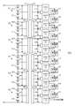
- FIG. 1 is a diagram illustrating a configuration of a power supply device 500 according to a comparative example.
- the power supply device 500 includes a battery unit 200 and a management unit 100.
- the battery unit 200 includes a series battery group 20 in which a plurality of lithium ion battery cells (hereinafter simply referred to as battery cells) are connected in series.
- the series battery group 20 is formed by a plurality of assembled batteries connected in series. Each assembled battery is formed by a plurality of battery cells connected in series.
- a harness connector is provided for each assembled battery.
- the electrodes of the plurality of battery cells forming the assembled battery and the plurality of terminals included in the harness connector are connected by wiring.
- the plurality of terminals included in the harness connector serve as output terminals of the plurality of battery cells forming the assembled battery.
- the management unit 100 includes a plurality of ASICs (Application Specific Integrated Circuit) connected in cascade. At least one ASIC is provided for each assembled battery.
- the ASIC is a dedicated custom IC for managing a plurality of battery cells included in the assembled battery.
- the ASIC has at least a function of detecting voltages at both ends of each of the plurality of battery cells included in the assembled battery.
- the ASIC includes a plurality of input terminals for detecting voltages at both ends of the plurality of battery cells.
- a board connector is provided for each at least one ASIC that manages one assembled battery.
- the plurality of input terminals provided in the at least one ASIC and the plurality of terminals of the board connector are connected by wiring.
- the plurality of terminals included in the board connector are input terminals of the at least one ASIC.
- one harness connector When the assembled battery is formed of x (x is an integer of 2 or more) battery cells, one harness connector includes at least (x + 1) voltage output terminals. When one assembled battery is managed by n (n is a natural number) ASICs, the number m (m is an integer of 2 or more) of management cells of one ASIC is x / n. One harness connector includes at least (m + 1) voltage input terminals.
- the power supply voltage and ground voltage of the ASIC are supplied from both ends of the m battery cells being managed. That is, the ASIC operates with the highest voltage of the series battery group formed by the m battery cells being managed as the power supply voltage and the lowest voltage as the ground voltage.
- the ground terminal of a certain ASIC is connected to the power supply terminal of an adjacent ASIC.
- Adjacent ASICs are connected by a communication line and can communicate with each other. At least one of the plurality of ASICs is connected to the control circuit.
- the control circuit acquires the voltage value of each battery cell from a plurality of ASICs, and performs battery control such as cell voltage equalization control with reference to the voltage value.
- the voltage of each battery cell is 4V
- the number x of battery cells forming one unit assembled battery is 12
- the number of assembled batteries forming the whole series battery group 20 is 6
- the number n of ASICs that manage a unit assembled battery is two
- the voltage of each assembled battery is about 50V
- the voltage of the whole series battery group 20 is about 300V.
- the first ASIC (1) and the second ASIC (2) are mounted on one substrate.
- This board includes a first board connector 41.
- the first assembled battery 21 and the substrate are mounted on one cell stack.
- the first harness connector 31 and the first board connector 41 are connected.
- the first assembled battery 21 may be formed by connecting two assembled batteries in series. In the above-described example, two unit batteries formed by six battery cells may be connected to form a new unit assembled battery formed by twelve battery cells.
- FIG. 1 only the wiring for supplying the power supply voltage and ground voltage of the ASIC from the assembled battery to the ASIC is illustrated.
- FIG. 1 since one assembled battery is managed by two ASICs, there is one intermediate power supply line. When managed by one ASIC, there are no intermediate power lines, and when managed by three ASICs, there are two intermediate power lines.
- the first assembled battery 21 includes a plurality (12 in the above example) of battery cells 211 to 21x.
- the highest voltage of the plurality of battery cells 211 to 21x is supplied to the power supply terminal of the first ASIC (1), and the intermediate voltage is supplied to the ground terminal of the first ASIC (1) and the power supply terminal of the second ASIC (2).
- the lowest voltage is supplied to the ground terminal of the second ASIC (2).
- the first ASIC (1) only needs to have a withstand voltage design corresponding to the voltage V1a that is half the voltage V1 across the plurality of battery cells 211 to 21x. In the above example, it is sufficient to have a breakdown voltage with a margin added to about 25V.
- the second ASIC (2) only needs to have a withstand voltage design corresponding to the voltage V1b that is half the voltage V1 across the plurality of battery cells 211 to 21x.
- the terminals of the first harness connector 31 and the terminals of the first board connector 41 are not necessarily ideally in contact with each other at the same time. If the terminal contact of the intermediate power line is delayed from the terminal contact of the power line of the first ASIC (1) and the terminal contact of the ground line of the second ASIC (2), it is formed by the first ASIC (1) and the second ASIC (2). A state in which the voltage V1 across the battery cells 211 to 21x is applied to the series circuit is instantaneously generated.
- ASIC impedance varies from one semiconductor wafer to another, and even ASICs generated from the same wafer have process variations. Therefore, it is not always the case that the voltage is divided cleanly by the number of series like the resistance voltage division. That is, 1/2 ⁇ V1 is not necessarily applied to each of the first ASIC (1) and the second ASIC (2). For example, it may occur that 1/4 ⁇ V1 is applied to the first ASIC (1) and 3/4 ⁇ V1 is applied to the second ASIC (2). In this case, the second ASIC (2) is over withstand voltage.
- the breakdown voltage is designed so that a margin is added to about 50V. If each withstand voltage of the first ASIC (1) and the second ASIC (2) is designed corresponding to the voltage V1 across the battery cells 211 to 21x, the voltage dividing ratio of the first ASIC (1) and the second ASIC (2) No matter what the value is, it is possible to avoid overvoltage resistance.
- the assembled battery is normally assembled with a low charging rate. Therefore, in the above configuration, the value of the charging rate at the time of assembly can be taken into consideration. That is, since the voltage of the unit assembled battery is low when the charging rate is low, the withstand voltage of the ASIC during assembly may be configured to be lower than the total voltage of the unit assembled battery. For example, when assembling the assembled battery in a state where the charging rate is 30%, the withstand voltage of the ASIC is set so as to withstand the voltage sum of the unit assembled battery in the state where the charging rate is 30%.
- the withstand voltage of the ASIC can be further reduced, and the over-withstand voltage at the time of assembly and maintenance of the power supply device can be reduced. Can be suppressed.
- the ASIC will withstand the breakdown voltage. It will never be over.
- the illustrated charging rate of 30% is merely an example, and is not necessarily set to this value, and can be selected as appropriate.
- each ASIC is included in the unit assembled battery in a state where the plurality of battery cells included in the series battery group are charged to a charging rate of less than 100%, more specifically, less than 50%. It can be designed to have a withstand voltage corresponding to the voltage across the battery cells.
- the charging rate may be a set charging rate at the time of assembling the assembled battery.
- the number m of battery cells managed by each ASIC is designed to be less than the ASIC withstand voltage. That is, the number of battery cells is determined so that the voltage across the plurality of battery cells connected in series managed by one ASIC is less than the withstand voltage of the ASIC.
- FIG. 2 is a diagram illustrating a state when the power supply device 500 according to the comparative example is assembled. As shown in FIG. 2, after the first harness connector 31 and the first board connector 41 are connected, the second harness connector 32 and the second board connector 42 are not connected, but the third harness connector 33 and the third board connector 42 are connected. The case where the board connector 43 is connected may occur.
- the ground terminal voltage of the second ASIC (2) is determined by the lowest voltage of the first assembled battery 21. Therefore, the power supply terminal voltage of the third ASIC (3) is also determined.
- the third harness connector 33 and the third board connector 43 are connected. At this time, the terminals of the third harness connector 33 and the third board connector 43 do not necessarily contact each other ideally at the same time.
- the ASIC impedance varies. Therefore, in the first case, the voltage of (V2 + V3) / 4 is not necessarily applied to each of the third ASIC (3), the fourth ASIC (4), the fifth ASIC (5), and the sixth ASIC (6). In the second case, a voltage of (V2 + (1/2 ⁇ V3)) / 3 is not necessarily applied to each of the third ASIC (3), the fourth ASIC (4), and the fifth ASIC (5). In the third case, the voltage V2 / 2 is not necessarily applied to each of the third ASIC (3) and the fourth ASIC (4).
- This over-voltage occurs when the intermediate potential of a series circuit formed by two or more ASICs is indefinite and the potential at both ends of the series circuit is determined. Therefore, this overvoltage will not occur if the connectors are connected in order from the high potential side or the low potential side.
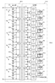
- FIG. 3 is a diagram showing a configuration of the power supply device 500 according to Embodiment 1 of the present invention.
- communication paths between adjacent ASICs are formed by non-insulated interfaces 51 to 61.
- the non-insulating interfaces 51 to 61 are electric wirings through level shift circuits. Therefore, a current flows directly between adjacent ASICs via a communication path.
- the communication path between adjacent ASICs sharing the board connector is the same as that of the power supply device 500 according to the comparative example. 57, 59, 61.
- a communication path between adjacent ASICs that do not share a board connector is formed by mixing non-insulating interfaces 52, 56, and 60 and insulating interfaces 54a and 58a.
- the ASICs connected by the insulation interfaces 54a and 58a are not connected by a power line common to both ASICs.
- the fourth ASIC (4) and the fifth ASIC (5) that do not share the board connector are connected by an insulating interface 54a, and the ground terminal of the fourth ASIC (4) and the power supply terminal of the fifth ASIC (5) are connected to the management unit 100. Is not connected.
- the insulation interfaces 54a and 58b may be configured to include a small transformer. By adopting a pulse modulation method for the communication signal, the transformer can be electrically insulated and level-shifted between the primary side coil and the secondary side coil.
- the insulation interfaces 54a and 58 may include a photocoupler. By transmitting and receiving communication signals between the ASICs as optical signals, the ASICs can be easily electrically insulated without adopting a complicated modulation method.
- the overvoltage resistance of the ASIC due to an error in the connector connection order occurs when the potential between both ends of the series circuit is determined while the intermediate potential of the series circuit formed by two or more ASICs is indefinite. This state occurs when at least one of the harness connector and the board connector is skipped and connected.
- the occurrence of the above-described state can be suppressed by insulating at least one of them. Therefore, it is possible to suppress the ASIC withstand voltage exceeding due to an error in the connector connection order.
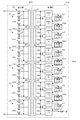
- FIG. 4 is a diagram showing a configuration of a power supply device 500 according to Embodiment 2 of the present invention.
- the communication path between adjacent ASICs sharing the board connector is the same as that of the power supply device 500 according to the first embodiment, and the non-insulated interfaces 51, 53, 55, 57, 59, 61.
- the communication paths between adjacent ASICs that do not share the board connector are all formed by the insulating interfaces 52a, 54a, 56a, 58a, and 60a.
- the power supply apparatus 500 is designed so that the withstand voltage of one ASIC exceeds the voltage across the assembled battery connected to one harness connector. As a result, it is possible to suppress the ASIC withstand voltage over which may occur when one harness connector is connected to one board connector. This is because, in principle, a voltage higher than the voltage across the assembled battery connected to one harness connector is not applied to one ASIC.
- the isolated interface uses a more expensive element than the non-isolated interface, which increases the cost. Therefore, an increase in cost can be suppressed as the use of the insulation interface is reduced.
- the first embodiment is an example in which the overvoltage resistance of the ASIC is suppressed with a minimum insulation interface.
- the second embodiment is an example in which the breakdown voltage of the ASIC is suppressed by a substrate having the same configuration. Even in the latter case, ASICs on the same substrate are formed with non-insulated interfaces. In the latter case, the types of substrates can be reduced, which is advantageous for mass production.
- 500 power supply 200 battery unit, 21-26 battery pack, 31-36 harness connector, 100 management unit, 41-46 board connector, 1-12, ASIC, 51-61 non-insulated interface, 52a, 54a, 56a, 58a 60a Isolated interface.
Landscapes
- Engineering & Computer Science (AREA)
- Power Engineering (AREA)
- Manufacturing & Machinery (AREA)
- Chemical & Material Sciences (AREA)
- Chemical Kinetics & Catalysis (AREA)
- Electrochemistry (AREA)
- General Chemical & Material Sciences (AREA)
- Life Sciences & Earth Sciences (AREA)
- Sustainable Development (AREA)
- Sustainable Energy (AREA)
- Transportation (AREA)
- Mechanical Engineering (AREA)
- Microelectronics & Electronic Packaging (AREA)
- Charge And Discharge Circuits For Batteries Or The Like (AREA)
- Secondary Cells (AREA)
- Electric Propulsion And Braking For Vehicles (AREA)
Abstract
電源装置の組み立て時およびメンテナンス時の耐圧オーバーを低コストで抑制する。 電源装置(500)において、複数の電池セルが直列に接続される。複数のセル管理ICはカスケード接続される。複数の電池セルの各端子と複数のセル管理ICの各端子は、電池側コネクタ及びIC側コネクタを介して接続される。IC側コネクタを共有するセル管理IC間は非絶縁通信される。IC側コネクタを共有しないセル管理IC間は絶縁通信される。
Description
本発明は、複数の電池セルが直列に接続された組電池を搭載した電源装置、およびその複数の電池セルを管理するための管理装置に関する。
近年、ハイブリッド車(HV)、プラグインハイブリッド車(PHV)、電気自動車(EV)が普及してきている。これらの車にはキーデバイスとして二次電池が搭載される。車載用二次電池としては主に、ニッケル水素電池およびリチウムイオン電池が普及している。今後、エネルギー密度が高いリチウムイオン電池の普及が加速すると予想される。
リチウムイオン電池は常用領域と使用禁止領域が近接しているため、他の種類の電池より厳格な電圧管理が必要である。複数のリチウムイオン電池セルが直列に接続された組電池を使用する場合、各電池セルの電圧を検出するための電圧検出回路が設けられる。検出される各電池セルの電圧は、充放電制御およびセル電圧の均等化制御などに使用される。
車載用の二次電池では高出力電圧が要求されるため、複数の組電池を直列に接続して使用されることが多い。この場合において複数の組電池と並列に、それぞれ電圧検出回路を実装した複数のICチップをカスケード接続して設ける構成が用いられる場合がある。
複数の組電池と、カスケード接続された複数のICチップを接続して電源装置を組み立てる際、組電池とICチップの接続順番によっては特定のICチップに耐圧オーバーの電圧が印加される可能性がある。この耐圧オーバーは電源装置のメンテナンス時にも発生し得る。この耐圧オーバーはICチップを高耐圧に設計すれば抑制できるが、コスト増を招く。
本発明はこうした状況に鑑みなされたものであり、その目的は、電源装置の組み立て時およびメンテナンス時の耐圧オーバーを低コストで抑制する技術を提供することにある。
上記課題を解決するために、本発明のある態様の電源装置は、複数の電池セルが直列に接続された直列電池群と、前記直列電池群に含まれる複数の電池セルを、m(mは2以上の整数)個ごとに管理する複数のセル管理IC(Integrated Circuit)と、前記複数の電池セルのm×n(nは自然数)個ごとに設けられ、m×n個の電池セルのそれぞれの端子を含む電池側コネクタと、前記複数のセル管理ICのn個ごとに設けられ、n個のセル管理ICのそれぞれの端子を含むIC側コネクタと、を備える。前記セル管理ICの電源電圧およびグラウンド電圧は、管理しているm個の電池セルの両端から供給を受け、前記複数のセル管理ICはカスケード接続され、前記IC側コネクタを共有するセル管理IC間は非絶縁通信され、前記IC側コネクタを共有しないセル管理IC間は絶縁通信される。
本発明の別の態様もまた、電源装置である。この装置は、複数の電池セルが直列に接続された直列電池群と、前記直列電池群に含まれる複数の電池セルを、m(mは2以上の整数)個ごとに管理する複数のセル管理IC(Integrated Circuit)と、前記複数の電池セルのm×n(nは自然数)個ごとに設けられ、m×n個の電池セルのそれぞれの端子を含む電池側コネクタと、前記複数のセル管理ICのn個ごとに設けられ、n個のセル管理ICのそれぞれの端子を含むIC側コネクタと、を備える。前記セル管理ICの電源電圧およびグラウンド電圧は、管理しているm個の電池セルの両端から供給を受け、前記複数のセル管理ICはカスケード接続され、前記IC側コネクタを共有するセル管理IC間は非絶縁通信され、前記IC側コネクタを共有しないセル管理IC間は、絶縁通信される箇所と非絶縁通信される箇所が混在される。
本発明のさらに別の態様は、管理装置である。この装置は、複数の電池セルが直列に接続された直列電池群を管理する管理装置であって、前記直列電池群に含まれる複数の電池セルを、m(mは2以上の整数)個ごとに管理する複数のセル管理IC(Integrated Circuit)と、前記複数の電池セルのm×n(nは自然数)個ごとに設けられ、m×n個の電池セルのそれぞれの端子を含む電池側コネクタと接続されるべきコネクタであって、前記複数のセル管理ICのn個ごとに設けられ、n個のセル管理ICのそれぞれの端子を含むIC側コネクタと、を備える。前記セル管理ICの電源電圧およびグラウンド電圧は、管理しているm個の電池セルの両端から供給を受け、前記複数のセル管理ICはカスケード接続され、前記IC側コネクタを共有するセル管理IC間は非絶縁通信され、前記IC側コネクタを共有しないセル管理IC間は絶縁通信される。
本発明のさらに別の態様もまた、管理装置である。この装置は、複数の電池セルが直列に接続された直列電池群を管理する管理装置であって、前記直列電池群に含まれる複数の電池セルを、m(mは2以上の整数)個ごとに管理する複数のセル管理IC(Integrated Circuit)と、前記複数の電池セルのm×n(nは自然数)個ごとに設けられ、m×n個の電池セルのそれぞれの端子を含む電池側コネクタと接続されるべきコネクタであって、前記複数のセル管理ICのn個ごとに設けられ、n個のセル管理ICのそれぞれの端子を含むIC側コネクタと、を備える。前記セル管理ICの電源電圧およびグラウンド電圧は、管理しているm個の電池セルの両端から供給を受け、前記複数のセル管理ICはカスケード接続され、前記IC側コネクタを共有するセル管理IC間は非絶縁通信され、前記IC側コネクタを共有しないセル管理IC間は、絶縁通信される箇所と非絶縁通信される箇所が混在される。
本発明によれば、電源装置の組み立て時およびメンテナンス時の耐圧オーバーを低コストで抑制できる。
図1は、比較例に係る電源装置500の構成を示す図である。電源装置500は電池部200および管理部100を備える。電池部200は複数のリチウムイオン電池セル(以下、単に電池セルという)が直列に接続された直列電池群20を備える。直列電池群20は、直列に接続された複数の組電池により形成される。各組電池は、直列に接続された複数の電池セルにより形成される。
組電池ごとにハーネスコネクタが設けられる。組電池を形成する複数の電池セルのそれぞれの電極とハーネスコネクタに含まれる複数の端子は配線で接続される。当該ハーネスコネクタに含まれる複数の端子は、組電池を形成する複数の電池セルのそれぞれの出力端子となる。
管理部100は、カスケード接続された複数のASIC(Application Specific Integrated Circuit)を備える。ASICは組電池ごとに少なくとも一つ設けられる。ASICは組電池に含まれる複数の電池セルを管理するための専用のカスタムICである。ASICは、組電池に含まれる複数の電池セルのそれぞれの両端電圧を検出する機能を少なくとも備える。ASICは、複数の電池セルのそれぞれの両端電圧を検出するための複数の入力端子を備える。
一つの組電池を管理する少なくとも一つのASICごとに、基板コネクタが設けられる。当該少なくとも一つのASICに設けられる複数の入力端子と、基板コネクタの複数の端子は配線で接続される。当該基板コネクタに含まれる複数の端子は、当該少なくとも一つのASICのそれぞれの入力端子となる。
組電池がx(xは2以上の整数)個の電池セルにより形成される場合、一つのハーネスコネクタは、少なくとも(x+1)本の電圧出力端子を備えることになる。一つの組電池をn(nは自然数)個のASICで管理する場合、一つのASICの管理セル数m(mは2以上の整数)は、x/n個となる。一つのハーネスコネクタは、少なくとも(m+1)本の電圧入力端子を備えることになる。
ASICの電源電圧およびグラウンド電圧は、管理しているm個の電池セルの両端から供給を受ける。即ちASICは、管理しているm個の電池セルにより形成される直列電池群の最上位電圧を電源電圧とし、最下位電圧をグラウンド電圧として動作する。あるASICのグラウンド端子は、隣接するASICの電源端子と接続される。
隣接するASIC間は通信線により接続され、相互に通信可能な構成である。また複数のASICの少なくとも一つは制御回路に接続される。当該制御回路は複数のASICから各電池セルの電圧値を取得し、その電圧値を参照してセル電圧の均等化制御などの電池制御を行う。
以下、本明細書では各電池セルの電圧が4V、1つの単位組電池を形成する電池セルの数xが12個、全体の直列電池群20を形成する組電池の数が6個、一つの単位組電池を管理するASICの数nが2個、1つのASICが管理するセル数mが6個の例を想定する。即ち、x=12、m=6、n=2の例を想定する。この例では各組電池の電圧が約50V、全体の直列電池群20の電圧が約300Vである。
図1において第1ASIC(1)および第2ASIC(2)は一つの基板に実装される。この基板は第1基板コネクタ41を備える。第1組電池21および当該基板は一つのセルスタックに搭載される。その際、第1ハーネスコネクタ31と第1基板コネクタ41が接続される。なお第1組電池21は、2個の組電池が直列に接続されて形成されてもよい。上述の例では6個の電池セルにより形成される組電池を2個接続して、12個の電池セルにより形成される新たな単位組電池を形成してもよい。
図1では組電池からASICへ、ASICの電源電圧およびグラウンド電圧となる電圧を供給する配線のみを描いている。図1では一つの組電池を二つのASICで管理するため、中間電源線は1本である。なお、一つのASICで管理する場合は中間電源線はなくなり、三つのASICで管理する場合は中間電源線が2本となる。
第1組電池21は複数(上述の例では12個)の電池セル211~21xを含む。この複数の電池セル211~21xの最上位電圧が第1ASIC(1)の電源端子に供給され、その中間電圧が第1ASIC(1)のグラウンド端子および第2ASIC(2)の電源端子に供給され、その最下位電圧が第2ASIC(2)のグラウンド端子に供給される。
第1ASIC(1)は原理的には、複数の電池セル211~21xの両端電圧V1の半分の電圧V1aに対応する耐圧設計であれば足りる。上述の例では約25Vにマージンを加えた耐圧を有すれば足りる。第2ASIC(2)も同様に原理的には、複数の電池セル211~21xの両端電圧V1の半分の電圧V1bに対応する耐圧設計であれば足りる。
しかしながら、第1ハーネスコネクタ31と第1基板コネクタ41を接続する際、第1ハーネスコネクタ31の各端子と、第1基板コネクタ41の各端子が理想的に同時に接触するとは限らない。中間電源線の端子接触が、第1ASIC(1)の電源線の端子接触および第2ASIC(2)のグラウンド線の端子接触より遅延した場合、第1ASIC(1)および第2ASIC(2)により形成される直列回路に、複数の電池セル211~21xの両端電圧V1が印加される状態が瞬間的に発生する。
ASICのインピーダンスは半導体ウェハごとに異なり、同一ウェハから生成されたASICであってもプロセスによるばらつきがある。したがって抵抗分圧のように、直列数によりきれいに分圧されるとは限らない。即ち、第1ASIC(1)および第2ASIC(2)のそれぞれに1/2・V1が印加されるとは限らない。例えば、第1ASIC(1)に1/4・V1が印加され、第2ASIC(2)に3/4・V1が印加されることも発生し得る。この場合、第2ASIC(2)は耐圧オーバーとなってしまう。
この対策として各ASICを、単位組電池に含まれるx(=m×n)個の電池セルの両端電圧に対応する耐圧を有するように設計する。上述の例では約50Vにマージンを加えた耐圧に設計する。第1ASIC(1)および第2ASIC(2)のそれぞれの耐圧を、複数の電池セル211~21xの両端電圧V1に対応して設計すれば、第1ASIC(1)および第2ASIC(2)の分圧比がどのような値になっても、耐圧オーバーを回避できる。
一方、通常、組電池の組立ては充電率が低い状態で行う。そのため、上述の構成において、組立て時における充電率の値を考慮することもできる。即ち、充電率が低いときは単位組電池の電圧が低いため、組立て時においてASICの耐圧が単位組電池の電圧総和を下回るように構成しても良い。例えば、充電率30%の状態で組電池の組立を行う場合は、充電率30%の状態の単位組電池の電圧総和に対して耐えられるようにASICの耐圧を設定する。このような構成によると、ハーネスの接続が充電率が低い状態で行われることを考慮することで、ASICの耐圧をさらに下げることができ、電源装置の組み立て時およびメンテナンス時の耐圧オーバーを低コストで抑制することができる。
なお、この構成において、組電池が充電されて電池電圧が上昇しても、すべてのハーネスが接続されている状態では、m個のセル電圧合計がASICの耐圧以下で使用されればASICが耐圧オーバーとなることはない。また、例示した充電率30%は、あくまで例示であり、必ずしもこの値とする必要はなく、適宜選択可能である。
このように各ASICを、上述の直列電池群に含まれる複数の電池セルが100%未満、より具体的には50%未満の充電率に充電されている状態において、単位組電池に含まれるx個の電池セルの両端電圧に対応する耐圧を有するように設計することができる。当該充電率は組電池の組立時の設定充電率であってもよい。
ASICの耐圧を所与のものとする場合、各ASICが管理する電池セル数mを、ASICの耐圧未満になるよう設計する。即ち、一つのASICにより管理される、直列接続される複数の電池セルの両端電圧が当該ASICの耐圧未満になるよう、電池セル数を決定する。
図2は、比較例に係る電源装置500の組み立て時の様子を示す図である。図2に示すように第1ハーネスコネクタ31と第1基板コネクタ41が接続された後、第2ハーネスコネクタ32と第2基板コネクタ42が接続されるのではなく、第3ハーネスコネクタ33と第3基板コネクタ43が接続される場合が発生し得る。
第1ハーネスコネクタ31と第1基板コネクタ41が完全に接続された状態において、第2ASIC(2)のグラウンド端子電圧は、第1組電池21の最下位電圧により確定する。したがって第3ASIC(3)の電源端子電圧も確定する。
その後、第3ハーネスコネクタ33と第3基板コネクタ43が接続される。その際、第3ハーネスコネクタ33と第3基板コネクタ43の各端子が理想的に同時に接触するとは限らない。
第6ASIC(6)のグラウンド線が一番先に端子接触した場合(第1ケース)、その瞬間、第3ASIC(3)、第4ASIC(4)、第5ASIC(5)および第6ASIC(6)により形成される直列回路の両端に、第2組電池22および第3組電池23により形成される直列電池群の両端電圧(V2+V3)が印加される。
また中間電源線が一番先に端子接触した場合(第2ケース)、その瞬間、第3ASIC(3)、第4ASIC(4)および第5ASIC(5)により形成される直列回路の両端に、第2組電池22および第3組電池23の上半分により形成される直列電池群の両端電圧(V2+(1/2・V3))が印加される。
また第5ASIC(5)の電源線が一番先に端子接触した場合(第3ケース)、その瞬間、第3ASIC(3)および第4ASIC(4)により形成される直列回路の両端に、第2組電池22の両端電圧V2が印加される。
上述したようにASICのインピーダンスには、ばらつきがある。したがって第1ケースでは、第3ASIC(3)、第4ASIC(4)、第5ASIC(5)および第6ASIC(6)のそれぞれに(V2+V3)/4の電圧が印加されるとは限らない。第2ケースでは第3ASIC(3)、第4ASIC(4)および第5ASIC(5)のそれぞれに(V2+(1/2・V3))/3の電圧が印加されるとは限らない。第3ケースでは第3ASIC(3)および第4ASIC(4)のそれぞれにV2/2の電圧が印加されるとは限らない。
上述の対策により第3ASIC(3)、第4ASIC(4)、第5ASIC(5)および第4ASIC(6)のそれぞれのASICの耐圧が、第2組電池22の両端電圧V2(=第3組電池23の両端電圧V3)より高く設計されていても、第1ケースおよび第2ケースでは、いずれかのASICに耐圧オーバーの電圧が印加される可能性がある。
この耐圧オーバーは、二つ以上のASICにより形成される直列回路の中間電位が不定な状態で、当該直列回路の両端電位が確定したとき発生する。したがって、この耐圧オーバーは、高電位側または低電位側から順番にコネクタを接続していけば発生しない。
組み立て工場の作業員のみであれば、このルールを徹底させることも可能であると考えられるが、自動車ディーラーなどを含むメンテナンス作業員やユーザにまで徹底させるのは極めて困難である。したがって複数のハーネスコネクタ31~36がどのような順番で、基板コネクタ41~46に接続されても、どのASIC(1)~(12)にも耐圧オーバーが発生しない仕組みが要求される。
図3は、本発明の実施の形態1に係る電源装置500の構成を示す図である。図1に示すように比較例に係る電源装置500では、隣接するASIC間の通信路は非絶縁インタフェース51~61で形成される。非絶縁インタフェース51~61はそれぞれレベルシフト回路を介した電気配線である。したがって、隣接するASIC間には通信路を介して直接、電流が流れる。
図3に示すように実施の形態1に係る電源装置500では、基板コネクタを共有する隣接するASIC間の通信路は、比較例に係る電源装置500と同様に非絶縁インタフェース51、53、55、57、59、61で形成される。基板コネクタを共有しない隣接するASIC間の通信路は、非絶縁インタフェース52、56、60と絶縁インタフェース54a、58aが混在して形成される。絶縁インタフェース54a、58aで接続されるASIC間は、両ASICに共通な電源線により接続されない。具体的には基板コネクタを共有しない第4ASIC(4)と第5ASIC(5)間は絶縁インタフェース54aで接続され、第4ASIC(4)のグラウンド端子と第5ASIC(5)の電源端子は管理部100では接続されない。第8ASIC(8)と第9ASIC(9)間も同様である。
絶縁インタフェース54a、58bは、小型のトランスを含む構成であってもよい。通信信号をパルス変調方式とすることにより、当該トランスの一次側コイルと二次側コイルの間で電気的に絶縁し、レベルシフトできる。また絶縁インタフェース54a、58はフォトカプラを含む構成であってもよい。ASIC間の通信信号を光信号で送受信することにより、ASIC間を複雑な変調方式を採用すること無く容易に電気的に絶縁できる。
基板コネクタを共有しないASIC間のうち、絶縁通信される箇所と非絶縁通信される箇所を交互に配置する。上述したようにコネクタの接続順番誤りによるASICの耐圧オーバーは、二つ以上のASICにより形成される直列回路の中間電位が不定な状態で、当該直列回路の両端電位が確定したとき発生する。この状態は、ハーネスコネクタと基板コネクタを、少なくとも一つ飛ばして接続する場合に発生する。
したがって基板をまたぐASIC間の接続において、少なくとも一つ飛ばして絶縁すれば上記状態の発生を抑制できる。よってコネクタの接続順番誤りによるASICの耐圧オーバーを抑制できる。
図4は、本発明の実施の形態2に係る電源装置500の構成を示す図である。実施の形態2に係る電源装置500でも、基板コネクタを共有する隣接するASIC間の通信路は、実施の形態1に係る電源装置500と同様に非絶縁インタフェース51、53、55、57、59、61で形成される。基板コネクタを共有しない隣接するASIC間の通信路は、実施の形態1に係る電源装置500と異なり全て絶縁インタフェース52a、54a、56a、58a、60aで形成される。
以上説明したように本発明の実施の形態1、2に係る電源装置500では、一つのASICの耐圧が、一つのハーネスコネクタに接続される組電池の両端電圧を超えるように設計する。これにより、一つのハーネスコネクタを一つの基板コネクタに接続する際に発生し得るASICの耐圧オーバーを抑制できる。一つのASICに、一つのハーネスコネクタに接続される組電池の両端電圧以上の電圧は原理的に印加されないためである。
また基板コネクタを共有しないASIC間の接続箇所を、少なくとも一つ飛ばしで絶縁することにより、ハーネスコネクタと基板コネクタをどのような順番で接続してもASICの耐圧オーバーが発生しないようにできる。
絶縁インタフェースは非絶縁インタフェースより高価な素子を使用するためコストが高くなる。したがって絶縁インタフェースの使用を少なくするほどコスト増大を抑制できる。実施の形態1はASICの耐圧オーバーを、最低限の絶縁インタフェースで抑制する例である。実施の形態2はASICの耐圧オーバーを、同じ構成の基板で抑制する例である。後者の場合でも同一基板内のASIC間は非絶縁インタフェースで形成される。後者の場合、基板の種類を減らすことができるため、量産化に有利である。
以上、本発明を実施の形態をもとに説明した。こられ実施の形態は例示であり、それらの各構成要素や各処理プロセスの組合せにいろいろな変形例が可能なこと、またそうした変形例も本発明の範囲にあることは当業者に理解されるところである。
500 電源装置、 200 電池部、 21~26 組電池、 31~36 ハーネスコネクタ、 100 管理部、 41~46 基板コネクタ、 1~12、 ASIC、 51~61 非絶縁インタフェース、52a、54a、56a、58a、60a 絶縁インタフェース。
Claims (6)
- 複数の電池セルが直列に接続された直列電池群と、
前記直列電池群に含まれる複数の電池セルを、m(mは2以上の整数)個ごとに管理する複数のセル管理IC(Integrated Circuit)と、
前記複数の電池セルのm×n(nは自然数)個ごとに設けられ、m×n個の電池セルのそれぞれの端子を含む電池側コネクタと、
前記複数のセル管理ICのn個ごとに設けられ、n個のセル管理ICのそれぞれの端子を含むIC側コネクタと、を備え、
前記セル管理ICの電源電圧およびグラウンド電圧は、管理しているm個の電池セルの両端から供給を受け、
前記複数のセル管理ICはカスケード接続され、前記IC側コネクタを共有するセル管理IC間は非絶縁通信され、前記IC側コネクタを共有しないセル管理IC間は絶縁通信されることを特徴とする電源装置。 - 複数の電池セルが直列に接続された直列電池群と、
前記直列電池群に含まれる複数の電池セルを、m(mは2以上の整数)個ごとに管理する複数のセル管理IC(Integrated Circuit)と、
前記複数の電池セルのm×n(nは自然数)個ごとに設けられ、m×n個の電池セルのそれぞれの端子を含む電池側コネクタと、
前記複数のセル管理ICのn個ごとに設けられ、n個のセル管理ICのそれぞれの端子を含むIC側コネクタと、を備え、
前記セル管理ICの電源電圧およびグラウンド電圧は、管理しているm個の電池セルの両端から供給を受け、
前記複数のセル管理ICはカスケード接続され、前記IC側コネクタを共有するセル管理IC間は非絶縁通信され、前記IC側コネクタを共有しないセル管理IC間は、絶縁通信される箇所と非絶縁通信される箇所が混在されることを特徴とする電源装置。 - 各セル管理ICは、前記複数の電池セルが所定の充電率に充電されている状態において、前記m×n個の電池セルの両端電圧に対応する耐圧を有することを特徴とする請求項1または2に記載の電源装置。
- 各セル管理ICは、前記複数の電池セルが所定の充電率に充電されている状態において、前記m×n個の電池セルの両端電圧に対応する耐圧を有し、
前記IC側コネクタを共有しないセル管理IC間のうち、絶縁通信される箇所と非絶縁通信される箇所が交互に配置されることを特徴とする請求項2に記載の電源装置。 - 複数の電池セルが直列に接続された直列電池群を管理する管理装置であって、
前記直列電池群に含まれる複数の電池セルを、m(mは2以上の整数)個ごとに管理する複数のセル管理IC(Integrated Circuit)と、
前記複数の電池セルのm×n(nは自然数)個ごとに設けられ、m×n個の電池セルのそれぞれの端子を含む電池側コネクタと接続されるべきコネクタであって、前記複数のセル管理ICのn個ごとに設けられ、n個のセル管理ICのそれぞれの端子を含むIC側コネクタと、を備え、
前記セル管理ICの電源電圧およびグラウンド電圧は、管理しているm個の電池セルの両端から供給を受け、
前記複数のセル管理ICはカスケード接続され、前記IC側コネクタを共有するセル管理IC間は非絶縁通信され、前記IC側コネクタを共有しないセル管理IC間は絶縁通信されることを特徴とする管理装置。 - 複数の電池セルが直列に接続された直列電池群を管理する管理装置であって、
前記直列電池群に含まれる複数の電池セルを、m(mは2以上の整数)個ごとに管理する複数のセル管理IC(Integrated Circuit)と、
前記複数の電池セルのm×n(nは自然数)個ごとに設けられ、m×n個の電池セルのそれぞれの端子を含む電池側コネクタと接続されるべきコネクタであって、前記複数のセル管理ICのn個ごとに設けられ、n個のセル管理ICのそれぞれの端子を含むIC側コネクタと、を備え、
前記セル管理ICの電源電圧およびグラウンド電圧は、管理しているm個の電池セルの両端から供給を受け、
前記複数のセル管理ICはカスケード接続され、前記IC側コネクタを共有するセル管理IC間は非絶縁通信され、前記IC側コネクタを共有しないセル管理IC間は、絶縁通信される箇所と非絶縁通信される箇所が混在されることを特徴とする管理装置。
Priority Applications (1)
| Application Number | Priority Date | Filing Date | Title |
|---|---|---|---|
| JP2014534185A JP6199294B2 (ja) | 2012-09-05 | 2013-09-03 | 電源装置および管理装置 |
Applications Claiming Priority (2)
| Application Number | Priority Date | Filing Date | Title |
|---|---|---|---|
| JP2012-195488 | 2012-09-05 | ||
| JP2012195488 | 2012-09-05 |
Publications (1)
| Publication Number | Publication Date |
|---|---|
| WO2014038180A1 true WO2014038180A1 (ja) | 2014-03-13 |
Family
ID=50236809
Family Applications (1)
| Application Number | Title | Priority Date | Filing Date |
|---|---|---|---|
| PCT/JP2013/005192 Ceased WO2014038180A1 (ja) | 2012-09-05 | 2013-09-03 | 電源装置および管理装置 |
Country Status (2)
| Country | Link |
|---|---|
| JP (1) | JP6199294B2 (ja) |
| WO (1) | WO2014038180A1 (ja) |
Cited By (1)
| Publication number | Priority date | Publication date | Assignee | Title |
|---|---|---|---|---|
| CN106505265A (zh) * | 2015-09-04 | 2017-03-15 | 丰田自动车株式会社 | 电压监视系统 |
Families Citing this family (2)
| Publication number | Priority date | Publication date | Assignee | Title |
|---|---|---|---|---|
| KR20200100967A (ko) | 2019-02-19 | 2020-08-27 | 주식회사 엘지화학 | Ic 칩 및 이를 이용한 회로 시스템 |
| KR102754697B1 (ko) | 2019-05-14 | 2025-01-13 | 주식회사 엘지에너지솔루션 | 배터리 관리 시스템 |
Citations (2)
| Publication number | Priority date | Publication date | Assignee | Title |
|---|---|---|---|---|
| JP2010141971A (ja) * | 2008-12-09 | 2010-06-24 | Mitsubishi Heavy Ind Ltd | 電池装置 |
| JP2010249793A (ja) * | 2009-02-27 | 2010-11-04 | Hitachi Ltd | 電池監視装置および電池監視装置の診断方法 |
-
2013
- 2013-09-03 WO PCT/JP2013/005192 patent/WO2014038180A1/ja not_active Ceased
- 2013-09-03 JP JP2014534185A patent/JP6199294B2/ja active Active
Patent Citations (2)
| Publication number | Priority date | Publication date | Assignee | Title |
|---|---|---|---|---|
| JP2010141971A (ja) * | 2008-12-09 | 2010-06-24 | Mitsubishi Heavy Ind Ltd | 電池装置 |
| JP2010249793A (ja) * | 2009-02-27 | 2010-11-04 | Hitachi Ltd | 電池監視装置および電池監視装置の診断方法 |
Cited By (1)
| Publication number | Priority date | Publication date | Assignee | Title |
|---|---|---|---|---|
| CN106505265A (zh) * | 2015-09-04 | 2017-03-15 | 丰田自动车株式会社 | 电压监视系统 |
Also Published As
| Publication number | Publication date |
|---|---|
| JPWO2014038180A1 (ja) | 2016-08-08 |
| JP6199294B2 (ja) | 2017-09-20 |
Similar Documents
| Publication | Publication Date | Title |
|---|---|---|
| JP6522513B2 (ja) | 電池管理装置および電源装置 | |
| US11626741B2 (en) | Management device and power supply system | |
| CN108494041B (zh) | 平衡校正装置及蓄电系统 | |
| US9219367B2 (en) | Method and apparatus for controlling a power supply device with aid of full-featured modularized functional blocks | |
| CN101789530B (zh) | 电池控制器的电位固定方式 | |
| JP6869966B2 (ja) | 管理装置および電源システム | |
| WO2013057820A1 (ja) | 電池システムの監視装置およびこれを備えた蓄電装置 | |
| CN109116262B (zh) | 电池监视系统、信号传输方法以及半导体装置 | |
| JP2009089453A (ja) | 電池監視回路および電池制御システム | |
| EP2239810A1 (en) | Battery pack and secondary battery system | |
| US9882491B2 (en) | Power supply system | |
| JP2014082152A (ja) | 電圧検出装置 | |
| EP3432409A1 (en) | Cell supervision circuit carrier, battery system and electric vehicle | |
| US20180231613A1 (en) | Semiconductor device and battery monitoring system | |
| JP6199294B2 (ja) | 電源装置および管理装置 | |
| US20140045004A1 (en) | Battery Management Unit Comprising a Plurality of Monitoring Units | |
| US20220123577A1 (en) | Battery control device | |
| US20170066343A1 (en) | Voltage monitoring system | |
| EP2517243B1 (en) | Hybrid circuit | |
| JPWO2017110049A1 (ja) | 電池管理システム | |
| EP3316389B1 (en) | Battery system, communication circuit for a battery system and vehicle | |
| US11204390B2 (en) | Battery monitoring circuit board and battery monitoring device | |
| Tarle et al. | Design of a battery management system for formula Student electric race vehicle | |
| JP5378290B2 (ja) | 蓄電システム | |
| US20200152947A1 (en) | Battery System Monitoring Device and Battery Pack |
Legal Events
| Date | Code | Title | Description |
|---|---|---|---|
| 121 | Ep: the epo has been informed by wipo that ep was designated in this application |
Ref document number: 13835265 Country of ref document: EP Kind code of ref document: A1 |
|
| ENP | Entry into the national phase |
Ref document number: 2014534185 Country of ref document: JP Kind code of ref document: A |
|
| NENP | Non-entry into the national phase |
Ref country code: DE |
|
| 122 | Ep: pct application non-entry in european phase |
Ref document number: 13835265 Country of ref document: EP Kind code of ref document: A1 |