WO2014037974A1 - カード挿入排出口ユニット、カード処理装置 - Google Patents
カード挿入排出口ユニット、カード処理装置 Download PDFInfo
- Publication number
- WO2014037974A1 WO2014037974A1 PCT/JP2012/005623 JP2012005623W WO2014037974A1 WO 2014037974 A1 WO2014037974 A1 WO 2014037974A1 JP 2012005623 W JP2012005623 W JP 2012005623W WO 2014037974 A1 WO2014037974 A1 WO 2014037974A1
- Authority
- WO
- WIPO (PCT)
- Prior art keywords
- card
- magnetic field
- card insertion
- discharge port
- port unit
- Prior art date
- Legal status (The legal status is an assumption and is not a legal conclusion. Google has not performed a legal analysis and makes no representation as to the accuracy of the status listed.)
- Ceased
Links
Images







Classifications
-
- G—PHYSICS
- G06—COMPUTING OR CALCULATING; COUNTING
- G06K—GRAPHICAL DATA READING; PRESENTATION OF DATA; RECORD CARRIERS; HANDLING RECORD CARRIERS
- G06K13/00—Conveying record carriers from one station to another, e.g. from stack to punching mechanism
- G06K13/02—Conveying record carriers from one station to another, e.g. from stack to punching mechanism the record carrier having longitudinal dimension comparable with transverse dimension, e.g. punched card
- G06K13/08—Feeding or discharging cards
-
- G—PHYSICS
- G07—CHECKING-DEVICES
- G07F—COIN-FREED OR LIKE APPARATUS
- G07F19/00—Complete banking systems; Coded card-freed arrangements adapted for dispensing or receiving monies or the like and posting such transactions to existing accounts, e.g. automatic teller machines
- G07F19/20—Automatic teller machines [ATMs]
-
- G—PHYSICS
- G07—CHECKING-DEVICES
- G07F—COIN-FREED OR LIKE APPARATUS
- G07F19/00—Complete banking systems; Coded card-freed arrangements adapted for dispensing or receiving monies or the like and posting such transactions to existing accounts, e.g. automatic teller machines
- G07F19/20—Automatic teller machines [ATMs]
- G07F19/205—Housing aspects of ATMs
-
- G—PHYSICS
- G07—CHECKING-DEVICES
- G07F—COIN-FREED OR LIKE APPARATUS
- G07F7/00—Mechanisms actuated by objects other than coins to free or to actuate vending, hiring, coin or paper currency dispensing or refunding apparatus
- G07F7/08—Mechanisms actuated by objects other than coins to free or to actuate vending, hiring, coin or paper currency dispensing or refunding apparatus by coded identity card or credit card or other personal identification means
- G07F7/0873—Details of the card reader
Definitions
- the present invention relates to a card insertion and ejection unit for inserting and ejecting cards, and a card processing apparatus provided with the unit.
- a transaction processing device such as an ATM (automatic cash dispenser) is equipped with a card processing device that processes information with respect to a magnetic card.
- the card processing apparatus takes in the magnetic card inserted from the card insertion and ejection port into the main body, and reads the magnetic information recorded on the magnetic stripe of the magnetic card with the magnetic head. Then, after the end of the transaction, the magnetic card is discharged from the inside of the main body to the card insertion and discharge port.
- an illegal device with a fake card insertion and ejection port equipped with a magnetic head is installed so as to cover a legitimate card insertion and ejection port, and a crime called skimming illegally acquires magnetic information of a magnetic card. is there.
- the magnetic field generating unit is composed of a coil and a loop antenna, and is installed in the front surface of the main body of the card processing apparatus or in a card slot unit installed on the front surface.
- a control unit that controls the drive of the magnetic field generation unit is installed in the main body.
- the card insertion and discharge port is exposed and disposed near the user, so it is easily damaged by unauthorized means.
- the magnetic field generating unit in the vicinity of the card insertion and discharge port is also easily damaged by an unauthorized means.
- An object of the present invention is to provide a card insertion and discharge port unit and a card processing device with improved maintainability while preventing unauthorized reading of magnetic information of a magnetic card.
- the card insertion and ejection port unit comprises an opening for inserting and ejecting the card, and a magnetic field generation unit for generating a disturbing magnetic field, and can be detachably attached to the card entry and exit portion of the main body of the card processor There is.
- a card processing apparatus comprises the above-mentioned card insertion discharge port unit, a magnetic reading unit for reading magnetic information recorded on a card in the main body, and a card transport unit for transporting the card in the main body.
- the card insertion and ejection port unit is attached to the card entry and exit portion of the main body of the card processing device, and the magnetic field generation unit generates the disturbing magnetic field to illegally read the magnetic information of the magnetic card by the illegal device ( Skimming) can be prevented. Further, by removing the card insertion and ejection port unit from the card entry and exit portion, maintenance work such as replacement, repair, and cleaning of the unit, the magnetic field generation unit, and the card entry and exit portion can be easily performed. Therefore, the maintainability of the card insertion and ejection port unit and the card processing apparatus can be improved.
- the card insertion and discharge port unit may further include a magnetic field control unit for controlling generation and stop of the disturbing magnetic field from the magnetic field generation unit.
- the maintainability of the magnetic field control unit can also be improved. Further, by arranging the magnetic field generation unit and the magnetic field control unit in the close state and connecting them by the shortest wiring path, it is possible to reduce the occurrence of unnecessary parasitic circuits due to the long wiring path. In addition, even if a high voltage is generated between the magnetic field generation unit and the magnetic field control unit, the risk of an electric shock and the like can be suppressed.
- the magnetic field generation unit may include a loop antenna, and the loop antenna may surround the periphery of the card entrance and exit portion.
- the loop antenna in the card insertion and ejection port unit, may be embedded in the unit with resin.
- the loop antenna is damaged or deformed by an illegal means such as a rod-like foreign object being thrust through the opening of the card insertion and discharge port unit or the hole made illegally in the transaction processing device housing covering the unit. It is possible to prevent the movement, the misalignment and the removal.
- the loop antenna is formed of a coil, it is possible to effectively prevent the deformation and disconnection of the coil by the above-mentioned illegal means. And it becomes possible to hold
- the outer dimensions of the loop antenna are 56 mm to 110 mm in width, 2 mm to 100 mm in height, and depth
- the dimensions in the loop portion of the loop antenna may be 55 mm to 109 mm in width, 1 mm to 99 mm in height, and 1 mm to 40 mm in depth.
- the dimensions of the loop antenna can be set in accordance with the dimensions of the card to be handled and the dimensions of each part of the card processing apparatus.
- the dimensions of the card insertion and discharge port unit can be set according to the dimensions of the loop antenna.
- the card insertion and discharge unit may further include a magnetic field changing member fixed in the unit and changing characteristics of the magnetic field radiated from the loop antenna.
- the magnetic field changing member is fixed in the card insertion and discharge port unit, it is possible to prevent the magnetic field changing member from being displaced or removed by unauthorized means.
- the magnetic field changing member may absorb a magnetic field directed from the loop antenna to the main body side of the card processing device.
- the magnetic field changing member may increase the magnetic field from the loop antenna to the side opposite to the main body of the card processing device.
- the magnetic field changing member may be a magnetic body made of ferrite, permalloy, silicon steel, iron, aluminum, or stainless steel.
- the characteristics of the disturbing magnetic field emitted from the loop antenna can be arbitrarily changed by appropriately setting the material, the size, the shape, and the arrangement of the magnetic field changing member. Further, by forming the magnetic field changing member so as to increase the rigidity, it is possible to prevent the magnetic field changing member from being damaged or deformed by unauthorized means, and the magnetic field changing function can be stably held. .
- the magnetic field changing member may cover the card insertion detection sensor provided at the card entry and exit portion from the outside.
- the magnetic field changing member can prevent the card insertion detection sensor from being damaged or deformed by unauthorized means. Also, the magnetic field from the loop antenna to the card insertion detection sensor can be reduced. Therefore, when the card insertion detection sensor is formed of a magnetic head, it is possible to prevent the deterioration of the detection performance of the magnetic information of the magnetic card by the magnetic head.
- FIG. 1 is an electrical block diagram of a card processing apparatus according to an embodiment of the present invention.
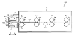
- FIG. 2 is a schematic structural view of the card processing apparatus of FIG.
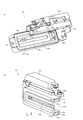
- FIG. 3 is an exploded view of a main body of the card processing apparatus of FIG. 1 and a card insertion and ejection port unit.
- FIG. 4 is an assembly view of the card processing apparatus of FIG.
- FIG. 5 is a perspective view of a card insertion and ejection port unit according to a first embodiment of the present invention.
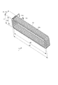
- FIG. 6 is a perspective view of a loop antenna according to a first embodiment of the present invention.
- FIG. 7 is a perspective view of a card slot unit according to a second embodiment of the present invention.
- FIG. 1 is an electrical block diagram of a card processing apparatus according to an embodiment of the present invention.
- FIG. 2 is a schematic structural view of the card processing apparatus of FIG.
- FIG. 3 is an exploded view of a main body of the card processing apparatus of FIG. 1 and a card
- FIG. 8 is a perspective view of a magnetic field changing member according to a second embodiment of the present invention.
- FIG. 9 is a structural view of the vicinity of the card insertion and discharge port unit of the card processing apparatus according to the second embodiment of the present invention.
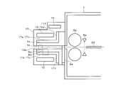
- FIG. 10 is a structural view of the vicinity of a card insertion and discharge port unit of a card processing apparatus according to another embodiment of the present invention.
- FIG. 11 is a view showing an arrangement example of an antenna according to another embodiment of the present invention.
- the card processing apparatus 100 is mounted on, for example, an ATM installed in a financial institution.
- the card processing apparatus 100 includes a card reader that receives the magnetic card 20 (FIG. 2) owned by the customer and reads the magnetic information recorded on the magnetic stripe of the magnetic card 20.
- the card processing apparatus 100 includes a main body 1 and a card insertion and ejection port unit 10.
- the main body 1 includes a control unit 2, a storage unit 3, a magnetic reading unit 4, a card conveyance unit 5, a card position detection sensor 6, a host interface 7, a card insertion detection sensor 8, and a shutter drive unit 9.
- the control unit 2, the storage unit 3, the magnetic reading unit 4, the card conveyance unit 5, the card position detection sensor 6, and the host interface 7 are provided inside the main body 1.
- the card insertion detection sensor 8 and the shutter drive unit 9 are provided on the outer side of the main body 1.
- the control unit 2 includes a microcomputer and controls the operation of each unit.
- the storage unit 3 includes a memory and stores various types of information.
- the magnetic reading unit 4 comprises a magnetic head 4a (FIG. 2) and a circuit (not shown) for driving the magnetic head 4a.
- the magnetic reading unit 4 reads magnetic information from the magnetic stripe of the magnetic card 20 by the magnetic head 4 a in the main body 1.
- the card conveyance unit 5 is composed of a plurality of rollers 5a (FIG. 2) and a motor or circuit (not shown) for rotating the rollers 5a.
- the card conveyance unit 5 sandwiches the magnetic card 20 between the rollers 5a in the main body 1, rotates the roller 5a by the driving force of the motor, and reciprocates the magnetic card 20.
- the card position detection sensor 6 is composed of a plurality of light sensors 6a (FIG. 2).
- the control unit 2 detects the position of the magnetic card 20 in the main body 1 based on the output state of each card position detection sensor 6.
- the host interface 7 is composed of a circuit that transmits and receives information to and from the ATM.
- the card insertion detection sensor 8 comprises a micro switch 8a (FIG. 2) and a small magnetic head 8b (FIG. 2).
- the control unit 2 detects the insertion of the magnetic card 20 into the card insertion and ejection port unit 10 based on the output state of the card insertion detection sensor 8.
- the shutter drive unit 9 is composed of a solenoid and a circuit (not shown) for opening and closing the shutter 9a (FIG. 2).
- the card insertion and discharge port unit 10 is provided with a magnetic field generation unit 11 and a magnetic field control unit 13.
- the magnetic field generation unit 11 includes a loop antenna 12 and a circuit (not shown) for driving the loop antenna 12.
- the magnetic field generation unit 11 causes the loop antenna 12 to emit a disturbing magnetic field by supplying a current to the loop antenna 12.
- the magnetic field control unit 13 is composed of a microcomputer.
- the magnetic field control unit 13 controls generation and stop of the disturbance magnetic field from the loop antenna 12 of the magnetic field generation unit 11.
- FIG. 5 shows a perspective view of the card insertion / discharge port unit 10 as viewed from the back side, and (b) shows a partially broken perspective view. The same applies to FIG. 7 described later.
- a card inlet / outlet portion 1 a is provided on the front surface 1 f of the main body 1 of the card processing apparatus 100.
- the card inlet / outlet portion 1a protrudes forward (in the direction T in FIG. 3), and an inlet / outlet 1b is formed at the center.
- the inlet / outlet 1b is in communication with the inside of the main body 1 as shown in FIG.
- the magnetic card 20 enters and exits the main body 1 through the entry and exit 1b.
- screw holes 1c are formed on both sides of the card entry / exit portion 1a.
- the depth direction of the inlet / outlet 1 b and the screw hole 1 c is parallel to the card insertion direction S.
- a microswitch 8a and a small magnetic head 8b are provided on the convex portion 1e at the tip of the card entry / exit portion 1a.
- the actuator 8c of the micro switch 8a projects from the left side into the inlet / outlet 1b in FIG. When the side edge of the magnetic card 20 inserted into the inlet / outlet 1b abuts on the actuator 8c, the micro switch 8a is turned ON, and it is detected that a card of a predetermined width is inserted.
- the small magnetic head 8b protrudes into the inlet / outlet 1b from below. By detecting the magnetic stripe of the magnetic card 20 inserted into the entry / exit 1b, the small magnetic head 8b detects that the card on which the magnetic information is recorded is inserted. Although the small magnetic head 8b may be affected by the disturbing magnetic field of the loop antenna 12, it is sufficient if the magnetic information can be detected at a predetermined level even if the magnetic information of the magnetic card 20 can not be read accurately. There is no problem in detection performance.
- FIG. 2 shows a state where the shutter 9a is lowered to open the inlet / outlet 1b. A state in which the shutter 9a is lifted and the inlet / outlet 1b is closed is shown in FIG. 9 described later.
- an opening 10 b for inserting and discharging the magnetic card 20 is formed at the center of the card insertion and discharge port unit 10.
- Through holes 10 c are formed on both sides of the card insertion and discharge port unit 10. The depth direction of the opening 10 b and the through hole 10 c is parallel to the card insertion direction S.
- a recess 10a is formed on the back side of the card insertion and discharge port unit 10. As shown in FIG. The recess 10a is in communication with the opening 10b. The size of the concave portion 10a is larger than the size of the convex portion 1e at the tip of the card entry / exit portion 1a shown in FIG.
- the card insertion discharge port unit 10 is provided with a loop antenna 12.
- the loop antenna 12 is embedded in the card insertion and ejection port unit 10 with resin 14 a and 14 b so as to surround the periphery of the recess 10 a with the loop portion 12 a.
- the resin 14 a is a synthetic resin having thermoplasticity, and constitutes a frame of the card insertion and discharge port unit 10.
- the resin 14 b is a synthetic resin such as epoxy that cures in a short time. After the loop antenna 12 is mounted on the mounting portion 10s (FIG. 5B) formed of the resin 14a, the resin 14b before curing is applied so as to cover the loop antenna 12. Then, the loop antenna 12 is embedded in the card insertion and discharge port unit 10 by curing the resin 14 b.
- the loop antenna 12 is composed of an air core coil wound with a copper wire as shown in FIG.
- the external dimensions of the loop antenna 12 as viewed from the card insertion direction S are 56 mm to 110 mm in width W1, 2 mm to 100 mm in height H1, and 1 mm to 40 mm in depth D1.
- the width W2 is 55 mm to 109 mm
- the vertical width H2 is 1 mm to 99 mm
- the depth D2 is 1 mm to 40 mm.
- the dimensions of the loop antenna 12 are set from the above-described range in consideration of the dimensions of the magnetic card 20, the card processing apparatus 100, and each part of the ATM.
- a substrate storage portion 10 d is provided on the top of the card insertion and ejection port unit 10 so as to protrude in the card insertion direction S.
- the substrate 15 is fixed in the substrate storage portion 10d.
- the lead 12 b of the loop antenna 12, the circuit of the magnetic field generation unit 11 of FIG. 1, and the magnetic field control unit 13 are mounted on the substrate 15.
- the substrate 15 and the loop antenna 12 are connected by the shortest wiring path.
- the convex portion 1e of the card inlet / outlet portion 1a and the concave portion 10a (FIG. 5A) of the card insertion / ejection port unit 10 are fitted. Then, the screw holes 1c of the card inlet / outlet portion 1a communicate with the through holes 10c of the card insertion / discharge port unit 10. Therefore, as shown in FIG. 4, the card insertion and ejection port unit 10 is formed by inserting a screw 16 into each through hole 10 c and screwing each through the through holes 10 c with a driver or the like (not shown). It is attached to the part 1a and is in a fixed state.
- the connector 18 a of the harness 18 exposed from the main body 1 is fitted to the connector 18 b mounted on the substrate 15 of the card insertion and ejection port unit 10 as shown in FIG. 4. Then, the main body 1 and the card insertion and ejection port unit 10 are electrically connected.
- the unit 10 covers the card entry / exit portion 1a, the micro switch 8a, and the small magnetic head 8b from the outside.
- the loop portion 12a of the loop antenna 12 surrounds the periphery of the card entry / exit portion 1a.
- the opening 10b of the card insertion and discharge port unit 10 and the inlet and outlet 1b of the card inlet and outlet portion 1a communicate with each other. Therefore, by inserting the magnetic card 20 in the S direction from the opening 10 b, the magnetic card 20 enters the main body 1 through the entrance / exit 1 b.
- the control unit 2 shown in FIG. 1 transmits a magnetic field generation command to the magnetic field control unit 13.
- the magnetic field generation unit 11 causes the loop antenna 12 to emit a disturbing magnetic field.
- the control unit 2 when the user stands in front of the ATM, an activation command is transmitted from the ATM to the card processing apparatus 100. Then, the control unit 2 having received the start-up command by the host interface 7 may transmit a magnetic field generation command to the magnetic field control unit 13 and cause the magnetic field generation unit 11 to emit the disturbing magnetic field. In this case, before or at the same time as the insertion of the magnetic card 20 into the card insertion and ejection port unit 10, the disturbance magnetic field is emitted by the magnetic field generation unit 11.
- the control unit 2 conveys the magnetic card 20 by the card conveyance unit 5 (FIG. 1).
- the magnetic field control unit 13 transmits a magnetic field stop command.
- the magnetic field generation unit 11 causes the radiation of the disturbance magnetic field from the loop antenna 12 to be stopped.
- the disturbance magnetic field may be stopped after being emitted for a predetermined time.
- the magnetic information of the magnetic card 20 is read by the magnetic reading unit 4 (FIG. 1).
- the card conveyance unit 5 conveys the magnetic card 20 to the card insertion / discharge port unit 10 through the card inlet / outlet portion 1a and is discharged from the opening 10b in the T direction (FIG. 2).
- the magnetic field control unit 13 may cause the loop antenna 12 to emit a disturbing magnetic field by the magnetic field generation unit 11.
- the card insertion / discharge port unit 10 can be inserted into the card inlet / outlet portion of the main body 1 by removing the screw 16 from each screw hole 1c and each through hole 10c with a driver or the like. It is possible to leave 1a. Further, by disconnecting the connector 18a from the connector 18b, the main body 1 and the card insertion discharge port unit 10 are electrically disconnected.
- the card insertion and ejection port unit 10 provided with the opening 10 b and the magnetic field generation unit 11 is attachable to and detachable from the card entry and exit portion 1 a of the main body 1 of the card processing apparatus 100. For this reason, the card insertion and ejection port unit 10 is attached to the card entry and exit portion 1a, and the magnetic field generation unit 11 generates a disturbing magnetic field, whereby illegal reading (skimming) of magnetic information of the magnetic card 20 by the illegal device is performed. It can be prevented.
- the card insertion and ejection port unit 10 is detached from the card entry and exit section 1a, thereby replacing the unit 10, the magnetic field generation section 11, the card entry and exit section 1a, the card insertion detection sensor 8 and the shutter drive section 9 and the like. Easy to do maintenance work such as repair and cleaning. Therefore, the maintainability of the card insertion and ejection port unit 10 and the card processing apparatus 100 can be improved.
- the magnetic field control unit 13 is provided in the card insertion and discharge port unit 10, the maintainability of the magnetic field control unit 13 can also be improved. Further, by arranging the loop antenna 12 of the magnetic field generation unit 11, the drive circuit, and the magnetic field control unit 13 in close proximity and connecting them by the shortest wiring path, generation of unnecessary parasitic circuits due to long wiring paths is reduced. Can. In addition, even if a high voltage is generated between the magnetic field generation unit 11 and the magnetic field control unit 13, the risk of an electric shock or the like can be suppressed.
- a loop antenna 12 surrounds the periphery of the card entry / exit portion 1a. For this reason, it is possible to generate a disturbing magnetic field with respect to the card entry / exit portion 1a and to prevent unauthorized reading of the magnetic information of the magnetic card 20 by the unauthorized device.
- the loop antenna 12 is embedded in the card insertion and discharge port unit 10 with the resins 14a and 14b. For this reason, even if a rod-like foreign object is thrust into the card insertion and discharge port unit 10 through the hole formed in the opening 10b or the case of the ATM, the loop antenna 12 is damaged or deformed by the incorrect means. Misalignment and removal can be prevented.
- the loop antenna 12 is formed of a coil as in the present embodiment, it is possible to effectively prevent the deformation and disconnection of the coil by the above-described illegal means.
- the dimensions of the loop antenna 12 can be adjusted according to the external dimensions of the card to be handled and the dimensions of each part of the card processing apparatus 100. It can be set.
- the card insertion and ejection port unit 10 is provided with a pair of magnetic field changing members 17a and 17b.
- the magnetic field changing members 17a and 17b are magnetic members made of ferrite, permalloy, silicon steel, iron, aluminum or stainless steel, and are formed in a shape as shown in FIG.
- the horizontal portions 17c of the magnetic field changing members 17a and 17b are inserted into the recesses 10a of the card insertion and ejection port unit 10 and held by the claws 10g, as shown in FIG. Further, the lock claws 17d of the magnetic field changing members 17a and 17b are fitted into the lock holes 10h of the card insertion and discharge port unit 10. Thereby, the magnetic field changing members 17 a and 17 b are fixed in the card insertion and discharge port unit 10.
- the card insertion / discharge port unit 10 provided with such magnetic field changing members 17a and 17b is attached to the card entry / exit portion 1a of the main body 1 of the card processing apparatus 100 as shown in FIG. Do. Then, as shown in FIG. 9, the horizontal portions 17c of the magnetic field changing members 17a and 17b cover the card inlet / outlet portion 1a from above and below. Between the loop antenna 12 and the main body 1, the vertical portions 17f of the magnetic field changing members 17a and 17b are interposed.
- the small magnetic head 8b is fitted into the notch 17e (FIG. 7) of the magnetic field changing member 17b (not shown). Other parts (not shown) fit into the notches 17 g of the magnetic field changing member 17 a (not shown).
- the magnetic field changing members 17 a and 17 b change the characteristics (distribution) of the magnetic field emitted from the loop antenna 12. Specifically, the vertical portions 17f of the magnetic field changing members 17a and 17b absorb the magnetic field directed from the loop antenna 12 toward the main body 1 side. Also, the horizontal portions 17c of the magnetic field changing members 17a and 17b increase the magnetic field from the loop antenna 12 to the side opposite to the main body 1.
- the characteristics such as the direction and the magnitude of the disturbance magnetic field radiated from the loop antenna 12 can be changed by the magnetic field change members 17a and 17b.
- directivity is given to the disturbing magnetic field radiated from the loop antenna 12 by the vertical portion 17f and the horizontal portion 17c of the magnetic field changing members 17a and 17b so that the disturbing magnetic field does not easily flow into the main body 1 of the card processing apparatus 100. can do. For this reason, it becomes possible to prevent the reading performance of the magnetic information of the magnetic card 20 by the magnetic head 4a provided in the main body 1 from being deteriorated by the disturbing magnetic field.
- the characteristics of the disturbing magnetic field radiated from the loop antenna 12 can be arbitrarily changed.
- the magnetic field changing members 17 a and 17 b are fixed in the card insertion and discharge port unit 10. For this reason, the magnetic field changing members 17a and 17b are dislocated or removed by an illegal means such as a rod-like foreign object being thrust through the hole 10b of the unit 10 or the case of the ATM. Can be prevented.
- the magnetic field changing members 17a and 17b are formed so as to increase the rigidity, the magnetic field changing members 17a and 17b are prevented from being damaged or deformed by unauthorized means, and the magnetic field changing function is stabilized. Can be held in
- the present invention can adopt various embodiments other than the embodiments described above.
- the second embodiment in order to avoid the collision with the small magnetic head 8b, the example in which the notch portion 17e is provided in the magnetic field changing member 17b is shown, but the present invention is not limited to this.
- the notch 17e may be omitted from the magnetic field changing member 17b, and the small magnetic head 8b may be covered from the outside with the magnetic field changing member 17b as shown in FIG. 10, for example.
- the magnetic field changing member 17b can prevent the small magnetic head 8b for detecting card insertion from being damaged or deformed by unauthorized means. Further, the magnetic field from the loop antenna 12 to the small magnetic head 8b can be reduced to prevent the deterioration of the magnetic detection performance of the small magnetic head 8b.
- the notch 17g (FIG. 8) of the magnetic field changing member 17a may be omitted.
- the loop antenna 12 is used to surround the opening 10b of the card insertion / ejection slot unit 10 and the card entry / exit portion 1a of the main body 1, but the present invention is limited thereto. It is not a thing. Other than this, for example, as shown by oblique lines in FIGS. 11A and 11B, upper portion A1, lower portion A2, left side portion A3, right side portion A4, and the card inlet / outlet portion 1a in the card insertion / discharge port unit 10. Alternatively, one or more magnetic field radiation antennas 12 'may be provided at any one or more locations in the front part A5.
- the antennas 12 and 12 'for magnetic field radiation are not limited to the loop antenna composed of coils, and may be, for example, a rod-like, plate-like or other antenna formed in a curved shape. Furthermore, without embedding the antenna 12, 12 'in the card insertion and discharge port unit 10 with resin, it is fixed by lock fitting like the magnetic field changing member 17a, 17b or fixed by a fixing member such as screw or adhesive. You may
- the present invention is not limited to this.
- a hook piece (not shown) provided on one of the card insertion / discharge port unit 10 and the card inlet / outlet portion 1 into a recess or a notch (not shown) provided on the other, card insertion / discharge
- the outlet unit 10 may be detachably attached to the card inlet / outlet portion 1a.
- the present invention is applied to the card processing device 100 and the card insertion and ejection port unit 10 dedicated to the magnetic card.
- the present invention can be applied to other card processing devices and card insertion and discharge port units which can handle, for example, any of a magnetic card, an IC card, and an IC card with a magnetic stripe.
Landscapes
- Physics & Mathematics (AREA)
- General Physics & Mathematics (AREA)
- Business, Economics & Management (AREA)
- Accounting & Taxation (AREA)
- Finance (AREA)
- Engineering & Computer Science (AREA)
- Theoretical Computer Science (AREA)
- Conveying Record Carriers (AREA)
- Credit Cards Or The Like (AREA)
- Control Of Vending Devices And Auxiliary Devices For Vending Devices (AREA)
Abstract
本体(1)内でカード搬送部(5)により磁気カード(20)を搬送して、磁気読み取り部(4)により磁気カード(20)に記録された磁気情報を読み取るカード処理装置(100)に、カード挿入排出口ユニット(10)を備える。カード挿入排出口ユニット(10)は、磁気カード(20)を挿入および排出する開口(10b)と、妨害磁界を発生する磁界発生部(11)とを備え、カード処理装置(100)の本体(1)のカード入出口部(1a)に対して着脱可能になっている。
Description
本発明は、カードを挿入および排出するカード挿入排出口ユニットと、該ユニットを備えたカード処理装置に関する。
ATM(現金自動預金支払機)などの取引処理装置には、磁気カードに対して情報の処理を行うカード処理装置が搭載されている。このカード処理装置は、カード挿入排出口から挿入された磁気カードを本体内に取り込んで、磁気カードの磁気ストライプに記録された磁気情報を磁気ヘッドで読み込む。そして、取引終了後に、磁気カードを本体内からカード挿入排出口へ排出する。
ATMにおいて、磁気ヘッドを備えた偽のカード挿入排出口を有する不正装置を、正規のカード挿入排出口に被せるように設置して、磁気カードの磁気情報を不正に取得する、スキミングと呼ばれる犯罪がある。
その対策として、たとえば特許文献1~3に開示されているように、磁界発生部により正規のカード挿入排出口の近傍に磁界を発生させて、不正装置の磁気ヘッドで磁気カードの磁気情報が読み取られるのを妨害する技術がある。
特許文献1~3では、磁界発生部は、コイルやループアンテナから成り、カード処理装置の本体前面部や、該前面部に設置されたカード挿入口ユニット内に設置されている。磁界発生部の駆動を制御する制御部は、本体内に設置されている。
カード挿入排出口は、露出していて、利用者に近い位置に配置されているため、不正な手段により破損され易い。また、カード挿入排出口の近傍にある磁界発生部も、不正な手段により破損され易い。しかしながら、カード挿入排出口や磁界発生部やこれらの周辺部分の保守作業を行うのは難しい。具体的には、カード挿入排出口や磁界発生部やこれらの近傍にあるセンサなどの交換、修理、および清掃などがし難い。
本発明の課題は、磁気カードの磁気情報の不正な読み取りを防止しつつ、保守性を向上させたカード挿入排出口ユニットおよびカード処理装置を提供することである。
本発明によるカード挿入排出口ユニットは、カードを挿入および排出する開口と、妨害磁界を発生する磁界発生部と、を備え、カード処理装置の本体のカード入出口部に対して着脱可能になっている。
また、本発明によるカード処理装置は、上記カード挿入排出口ユニットと、本体内でカードに記録された磁気情報を読み取る磁気読み取り部と、本体内でカードを搬送するカード搬送部とを備えている。
上記によると、カード挿入排出口ユニットをカード処理装置の本体のカード入出口部に装着して、磁界発生部により妨害磁界を発生させることで、不正装置による磁気カードの磁気情報の不正な読み取り(スキミング)を防止することができる。また、カード挿入排出口ユニットをカード入出口部から離脱させることで、当該ユニット、磁界発生部、およびカード入出口部などの交換、修理、および清掃などの保守作業を容易に行える。よって、カード挿入排出口ユニットやカード処理装置の保守性を向上させることができる。
また、本発明では、上記カード挿入排出口ユニットにおいて、磁界発生部からの妨害磁界の発生および停止を制御する磁界制御部を、さらに備えてもよい。
これにより、カード挿入排出口ユニットにおいて、磁界制御部の保守性も向上させることができる。また、磁界発生部と磁界制御部を接近状態で配置して、最短の配線経路で接続することで、長い配線経路による不要な寄生回路の発生を低減することができる。加えて、磁界発生部と磁界制御部の間に高電圧が発生しても、感電などの危険性を抑制することができる。
また、本発明では、上記カード挿入排出口ユニットにおいて、磁界発生部は、ループアンテナを含み、該ループアンテナは、カード入出口部の周囲を囲んでいてもよい。
これにより、カード処理装置の本体のカード入出口部に対して、妨害磁界を発生させて、不正装置による磁気カードの磁気情報の不正な読み取りを防止することができる。
また、本発明では、上記カード挿入排出口ユニットにおいて、ループアンテナは、樹脂で当該ユニット内に埋め込まれていてもよい。
これにより、カード挿入排出口ユニットの開口や、該ユニットを覆う取引処理装置の筐体に不正に空けた穴を通して、棒状の異物が突っ込まれるなどの不正な手段で、ループアンテナが損傷したり変形したり位置ずれしたり取り外されたりするのを防止することができる。特に、ループアンテナがコイルから成る場合には、上記のような不正な手段による、コイルの変形や断線を有効に防止することができる。そして、ループアンテナから放射される妨害磁界の向きを変えたり、妨害磁界を停止させたりする不正を阻止して、ループアンテナからの妨害磁界の放射機能を安定に保持することが可能となる。
また、本発明では、上記カード挿入排出口ユニットにおいて、カード挿入方向から見て、ループアンテナの外形寸法は、横幅が、56mm~110mmであり、縦幅が、2mm~100mmであり、奥行きが、1mm~40mmであり、ループアンテナのループ部内の寸法は、横幅が、55mm~109mmであり、縦幅が、1mm~99mmであり、奥行きが、1mm~40mmであってもよい。
これにより、取り扱うカードの外形寸法やカード処理装置の各部の寸法に応じて、ループアンテナの寸法を設定することができる。また、ループアンテナの寸法に応じて、カード挿入排出口ユニットの寸法を設定することができる。
また、本発明では、上記カード挿入排出口ユニットにおいて、当該ユニット内に固定され、ループアンテナから放射される磁界の特性を変化させる磁界変更部材を、さらに備えてもよい。
これにより、ループアンテナから放射された妨害磁界の向きや大きさなどの特性を、磁界変更部材で変化させることができる。また、磁界変更部材がカード挿入排出口ユニット内に固定されているので、不正な手段で磁界変更部材が位置ずれしたり取り外されたりするのを防止することができる。
また、本発明では、上記カード挿入排出口ユニットにおいて、磁界変更部材は、ループアンテナからカード処理装置の本体側へ向かう磁界を吸収してもよい。
これにより、ループアンテナから放射された妨害磁界に指向性を付与して、該妨害磁界をカード処理装置の本体内に及び難くすることができる。このため、本体内に備わる磁気読み取り部による磁気カードの磁気情報の読み取り性能が、妨害磁界により劣化するのを防止することが可能となる。
また、本発明では、上記カード挿入排出口ユニットにおいて、磁界変更部材は、ループアンテナからカード処理装置の本体と反対側へ向う磁界を増大させてもよい。
これにより、ループアンテナから放射された妨害磁界に指向性を付与して、該妨害磁界をカード処理装置の本体内に及び難くすることができる。このため、本体内に備わる磁気読み取り部による磁気カードの磁気情報の読み取り性能が、妨害磁界により劣化するのを防止することが可能となる。
また、本発明では、上記カード挿入排出口ユニットにおいて、磁界変更部材は、フェライト、パーマロイ、珪素鋼鈑、鉄、アルミニウム、またはステンレスから成る磁性体であってもよい。
これにより、磁界変更部材の材質、大きさ、形状、および配置を適宜設定することで、ループアンテナから放射された妨害磁界の特性を任意に変化させることができる。また、剛性が高くなるように、磁界変更部材を形成することで、不正な手段で磁界変更部材が損傷したり変形したりするのを防止して、磁界変更機能を安定に保持することができる。
さらに、本発明では、上記カード挿入排出口ユニットにおいて、磁界変更部材は、カード入出口部に設けられたカード挿入検知センサを外側から覆っていてもよい。
これにより、不正な手段でカード挿入検知センサが損傷したり変形したりするのを、磁界変更部材により阻止することができる。また、ループアンテナからカード挿入検知センサへ向かう磁界を減少させることができる。このため、カード挿入検知センサが磁気ヘッドから成る場合には、該磁気ヘッドによる磁気カードの磁気情報の検知性能が劣化するのを防止することが可能となる。
本発明によれば、磁気カードの磁気情報の不正な読み取りを防止しつつ、保守性を向上させたカード挿入排出口ユニットおよびカード処理装置を提供することが可能となる。
以下、本発明の実施形態につき、図面を参照しながら説明する。各図において、同一の部分または対応する部分には、同一符号を付してある。
まず、本発明の実施形態によるカード処理装置100の構成を、図1および図2を参照しながら説明する。
カード処理装置100は、たとえば、金融機関に設置されたATMに搭載される。カード処理装置100は、顧客が所有する磁気カード20(図2)を受け付けて、磁気カード20の磁気ストライプに記録された磁気情報を読み取るカードリーダから構成されている。
カード処理装置100は、本体1とカード挿入排出口ユニット10を備えている。本体1には、制御部2、記憶部3、磁気読み取り部4、カード搬送部5、カード位置検知センサ6、ホストインタフェイス7、カード挿入検知センサ8、およびシャッタ駆動部9が備わっている。
制御部2、記憶部3、磁気読み取り部4、カード搬送部5、カード位置検知センサ6、およびホストインタフェイス7は、本体1の内部に設けられている。カード挿入検知センサ8およびシャッタ駆動部9は、本体1の外側部に設けられている。
制御部2は、マイクロコンピュータから構成され、各部の動作を制御する。記憶部3は、メモリから構成され、各種の情報を記憶している。磁気読み取り部4は、磁気ヘッド4a(図2)と、該磁気ヘッド4aを駆動するための回路(図示省略)から構成されている。磁気読み取り部4は、本体1内で磁気ヘッド4aにより磁気カード20の磁気ストライプから磁気情報を読み取る。
カード搬送部5は、複数のローラ5a(図2)と、該ローラ5aを回転させるためのモータや回路(図示省略)から構成されている。カード搬送部5は、本体1内でローラ5a間に磁気カード20を挟み込み、モータの駆動力でローラ5aを回転させて、磁気カード20を往復搬送する。
カード位置検知センサ6は、複数の光センサ6a(図2)から構成されている。制御部2は、各カード位置検知センサ6の出力状態に基づいて、本体1内における磁気カード20の位置を検知する。ホストインタフェイス7は、ATMに対して情報を送受信する回路から構成されている。
カード挿入検知センサ8は、マイクロスイッチ8a(図2)および小型磁気ヘッド8b(図2)から構成されている。制御部2は、カード挿入検知センサ8の出力状態に基づいて、カード挿入排出口ユニット10への磁気カード20の挿入を検知する。シャッタ駆動部9は、シャッタ9a(図2)を開閉させるためのソレノイドや回路(図示省略)から構成されている。
カード挿入排出口ユニット10には、磁界発生部11と磁界制御部13が備わっている。磁界発生部11には、ループアンテナ12と、ループアンテナ12を駆動するための回路(図示省略)が含まれている。磁界発生部11は、ループアンテナ12に電流を流すことにより、ループアンテナ12から妨害磁界を放射させる。
磁界制御部13は、マイクロコンピュータから構成されている。磁界制御部13は、磁界発生部11のループアンテナ12からの妨害磁界の発生および停止を制御する。
次に、第1実施形態によるカード挿入排出口ユニット10の構造と、該ユニット10を取り付けるカード処理装置100の要部の構造を、図3~図6を参照しながら説明する。適宜、図1および図2も参照する。なお、図5では、カード挿入排出口ユニット10の裏側から見た斜視図を(a)に示し、一部破断斜視図を(b)に示している。後述する図7も同様である。
図3に示すように、カード処理装置100の本体1の前面1fには、カード入出口部1aが設けられている。カード入出口部1aは、前方(図3でT方向)へ突出していて、中央に入出口1bが形成されている。入出口1bは、図2に示すように、本体1内に連通している。磁気カード20は、入出口1bを通って、本体1内に対して入出する。
カード入出口部1aの両側部には、図3に示すように、ねじ孔1cが形成されている。入出口1bとねじ孔1cの奥行き方向は、カード挿入方向Sと平行である。
カード入出口部1aの先端の凸部1eには、マイクロスイッチ8aと小型磁気ヘッド8bが設けられている。マイクロスイッチ8aのアクチュエータ8cは、図3で左側から入出口1b内に突出している。入出口1bに挿入された磁気カード20の側縁がアクチュエータ8cに当接することで、マイクロスイッチ8aはON状態になり、所定の幅のカードが挿入されたことが検知される。
小型磁気ヘッド8bは、下方から入出口1b内に突出している。入出口1bに挿入された磁気カード20の磁気ストライプを検出することで、小型磁気ヘッド8bは磁気情報が記録されたカードが挿入されたことを検知する。なお、小型磁気ヘッド8bは、ループアンテナ12の妨害磁界の影響を受けるおそれがあるが、磁気カード20の磁気情報を正確に読み取れなくても、磁気情報を所定のレベルで検知できればよいので、該検知性能に支障はない。
シャッタ駆動部9(図1)の駆動力により、シャッタ9aを上下動させることにより、入出口1bが開放または閉鎖される。図2では、シャッタ9aが下降して、入出口1bを開放した状態を示している。シャッタ9aが上昇して、入出口1bを閉鎖した状態は、後述の図9に示している。
図3に示すように、カード挿入排出口ユニット10の中央には、磁気カード20を挿入および排出する開口10bが形成されている。カード挿入排出口ユニット10の両側部には、貫通孔10cが形成されている。開口10bと貫通孔10cの奥行き方向は、カード挿入方向Sと平行になっている。
図5(a)に示すように、カード挿入排出口ユニット10の裏側には、凹部10aが形成されている。凹部10aは、開口10bと連通している。凹部10aの大きさは、図3に示すカード入出口部1aの先端の凸部1eの大きさより大きくなっている。
カード挿入排出口ユニット10には、図5に示すように、ループアンテナ12が設けられている。ループアンテナ12は、ループ部12aで凹部10aの周囲を取り囲むように、樹脂14a、14bでカード挿入排出口ユニット10内に埋め込まれている。
詳しくは、樹脂14aは、熱可塑性を有する合成樹脂であり、カード挿入排出口ユニット10のフレームを構成している。樹脂14bは、短時間で硬化するエポキシなどの合成樹脂である。樹脂14aで形成された装着部10s(図5(b))にループアンテナ12を装着した後、該ループアンテナ12を覆うように、硬化前の樹脂14bを塗布する。そして、樹脂14bを硬化させることで、ループアンテナ12がカード挿入排出口ユニット10内に埋設される。
ループアンテナ12は、図6に示すような、銅線を巻き付けた空芯のコイルから構成されている。カード挿入方向Sから見た、ループアンテナ12の外形寸法は、横幅W1が、56mm~110mmであり、縦幅H1が、2mm~100mmであり、奥行きD1が、1mm~40mmである。また、ループアンテナ12のループ部12a内の寸法は、横幅W2が、55mm~109mmであり、縦幅H2が、1mm~99mmであり、奥行きD2が、1mm~40mmである。磁気カード20、カード処理装置100、およびATMの各部の寸法を考慮して、上記範囲からループアンテナ12の寸法を設定する。
図3に示すように、カード挿入排出口ユニット10の上部には、カード挿入方向Sへ突出するように、基板収納部10dが設けられている。基板収納部10d内には、図5(a)に示すように、基板15が固定されている。基板15には、ループアンテナ12のリード12b、図1の磁界発生部11の回路、および磁界制御部13が実装されている。基板15とループアンテナ12は、最短の配線経路で接続されている。
次に、カード処理装置100の本体1へのカード挿入排出口ユニット10の着脱方法と、カード処理装置100の動作を、図1~図5を参照しながら説明する。
図3に示す分離状態から、カード入出口部1aの凸部1eとカード挿入排出口ユニット10の凹部10a(図5(a))とを嵌め合わせる。すると、カード入出口部1aの各ねじ孔1cとカード挿入排出口ユニット10の各貫通孔10cとが連通する。このため、図示しないドライバなどにより、ねじ16を各貫通孔10cへ通して各ねじ孔1cに螺合することで、図4に示すように、カード挿入排出口ユニット10が本体1のカード入出口部1aに装着されて、固定状態となる。
また、図3に示すように、本体1から露出するハーネス18のコネクタ18aを、カード挿入排出口ユニット10の基板15に実装されたコネクタ18bに、図4に示すように嵌合する。すると、本体1とカード挿入排出口ユニット10とが電気的に接続される。
図2および図4に示す、カード挿入排出口ユニット10の装着状態では、該ユニット10が、カード入出口部1a、マイクロスイッチ8a、および小型磁気ヘッド8bを外側から覆っている。また、ループアンテナ12のループ部12aが、カード入出口部1aの周囲を囲んでいる。
さらに、カード挿入排出口ユニット10の開口10bと、カード入出口部1aの入出口1bとが連通している。このため、磁気カード20を開口10bからS方向に挿入することで、磁気カード20が入出口1bを通って、本体1内に進入して行く。
その際、マイクロスイッチ8aおよび小型磁気ヘッド8bにより磁気カード20の挿入を検知すると、図1に示す制御部2が、磁界制御部13に磁界発生指令を送信する。磁界制御部13は、磁界発生指令を受信すると、磁界発生部11によりループアンテナ12から妨害磁界を放射させる。
他の例として、利用者がATMの前に立ったときに、ATMからカード処理装置100に起動指令が送信される。そして、該起動指令をホストインタフェイス7により受信した制御部2が、磁界制御部13に磁界発生指令を送信し、磁界発生部11により妨害磁界を放射させてもよい。この場合、カード挿入排出口ユニット10への磁気カード20の挿入前から、または挿入と同時に、磁界発生部11により妨害磁界が放射される。
そして、カード位置検知センサ6(図1)により本体1内に磁気カード20が取り込まれたことを検知すると、制御部2が、カード搬送部5(図1)により磁気カード20を搬送し、かつ、磁界制御部13に磁界停止指令を送信する。磁界制御部13は、磁界停止指令を受信すると、磁界発生部11によりループアンテナ12からの妨害磁界の放射を停止させる。他の例として、妨害磁界を所定時間放射した後、停止してもよい。
この後、カード搬送部5により磁気カード20が搬送されながら、磁気読み取り部4(図1)により磁気カード20の磁気情報が読み取られる。そして、磁気カード20に対する処理が完了すると、カード搬送部5により磁気カード20が、カード入出口部1aを通してカード挿入排出口ユニット10へ搬送され、開口10bからT方向(図2)に排出される。このカード排出時に、磁界制御部13が、磁界発生部11によりループアンテナ12から妨害磁界を放射させてもよい。
カード処理装置100の保守時には、図4の装着状態から、ドライバなどにより、ねじ16を各ねじ孔1cと各貫通孔10cから外すことで、カード挿入排出口ユニット10は本体1のカード入出口部1aから離脱可能となる。また、コネクタ18aをコネクタ18bから抜くことで、本体1とカード挿入排出口ユニット10とが電気的に切断される。
上記第1実施形態によると、開口10bと磁界発生部11を備えたカード挿入排出口ユニット10が、カード処理装置100の本体1のカード入出口部1aに対して着脱可能になっている。このため、カード挿入排出口ユニット10をカード入出口部1aに装着して、磁界発生部11により妨害磁界を発生させることで、不正装置による磁気カード20の磁気情報の不正な読み取り(スキミング)を防止することができる。
また、カード挿入排出口ユニット10をカード入出口部1aから離脱させることで、当該ユニット10、磁界発生部11、カード入出口部1a、カード挿入検知センサ8、およびシャッタ駆動部9などの交換、修理、および清掃などの保守作業を容易に行える。よって、カード挿入排出口ユニット10やカード処理装置100の保守性を向上させることができる。
また、カード挿入排出口ユニット10に磁界制御部13が設けられているので、磁界制御部13の保守性も向上させることができる。また、磁界発生部11のループアンテナ12と駆動回路と磁界制御部13を接近状態で配置して、最短の配線経路で接続することで、長い配線経路による不要な寄生回路の発生を低減することができる。加えて、磁界発生部11と磁界制御部13の間に高電圧が発生しても、感電などの危険性を抑制することができる。
また、ループアンテナ12がカード入出口部1aの周囲を囲んでいる。このため、カード入出口部1aに対して、妨害磁界を発生させて、不正装置による磁気カード20の磁気情報の不正な読み取りを防止することができる。
また、ループアンテナ12が樹脂14a、14bでカード挿入排出口ユニット10内に埋め込まれている。このため、開口10bやATMの筐体に不正に空けた穴を通して、カード挿入排出口ユニット10内に棒状の異物が突っ込まれても、該不正な手段でループアンテナ12が損傷したり変形したり位置ずれしたり取り外されたりするのを防止することができる。特に、本実施形態のように、ループアンテナ12がコイルから成る場合には、上記のような不正な手段による、コイルの変形や断線を有効に防止することができる。
そして、ループアンテナ12から放射される妨害磁界の向きを変えたり、妨害磁界を停止させたりする不正を阻止して、ループアンテナ12からの妨害磁界の放射機能を安定に保持することが可能となる。
さらに、ループアンテナ12の外形寸法やループ部12a内の寸法を、前記のように選定することで、取り扱うカードの外形寸法やカード処理装置100の各部の寸法に応じて、ループアンテナ12の寸法を設定することができる。
次に、第2実施形態によるカード挿入排出口ユニット10の構造を、図7~図9を参照しながら説明する。適宜、図4も参照する。
第2実施形態では、前述した第1実施形態の構成に加えて、図7に示すように、カード挿入排出口ユニット10に一対の磁界変更部材17a、17bを備えている。磁界変更部材17a、17bは、フェライト、パーマロイ、珪素鋼鈑、鉄、アルミニウム、またはステンレスから成る磁性体であり、図8に示すような形状に形成されている。
磁界変更部材17a、17bの水平部17cを、図7に示すように、カード挿入排出口ユニット10の凹部10a内に挿入して、爪10gで保持する。また、磁界変更部材17a、17bのロック爪17dを、カード挿入排出口ユニット10のロック孔10hに嵌合する。これにより、磁界変更部材17a、17bが、カード挿入排出口ユニット10内に固定される。
このような、磁界変更部材17a、17bを備えたカード挿入排出口ユニット10を、図4に示すように、カード処理装置100の本体1のカード入出口部1aに装着して、ねじ16で固定する。すると、図9に示すように、磁界変更部材17a、17bの水平部17cがカード入出口部1aを上下方向から覆う。ループアンテナ12と本体1との間には、磁界変更部材17a、17bの垂直部17fが介在する。
磁界変更部材17bの切欠き部17e(図7)には、小型磁気ヘッド8bが嵌まり込む(図示省略)。磁界変更部材17aの切欠き部17gには、図示しない他の部品が嵌まり込む(図示省略)。
磁界変更部材17a、17bは、ループアンテナ12から放射される磁界の特性(分布)を変化させる。詳しくは、磁界変更部材17a、17bの垂直部17fが、ループアンテナ12から本体1側へ向かう磁界を吸収する。また、磁界変更部材17a、17bの水平部17cが、ループアンテナ12から本体1と反対側へ向う磁界を増大させる。
上記第2実施形態によると、ループアンテナ12から放射された妨害磁界の向きや大きさなどの特性を、磁界変更部材17a、17bで変化させることができる。特に、磁界変更部材17a、17bの垂直部17fや水平部17cにより、ループアンテナ12から放射された妨害磁界に指向性を付与して、該妨害磁界をカード処理装置100の本体1内に及び難くすることができる。このため、本体1内に備わる磁気ヘッド4aによる磁気カード20の磁気情報の読み取り性能が、妨害磁界により劣化するのを防止することが可能となる。
また、磁界変更部材17a、17bの材質、大きさ、形状、および配置を適宜設定することで、ループアンテナ12から放射された妨害磁界の特性を任意に変化させることができる。
また、磁界変更部材17a、17bが、カード挿入排出口ユニット10内に固定されている。このため、該ユニット10の開口10bやATMの筐体に不正に空けた穴を通して、棒状の異物が突っ込まれるなどの不正な手段で、磁界変更部材17a、17bが位置ずれしたり取り外されたりするのを防止することができる。
さらに、剛性が高くなるように、磁界変更部材17a、17bを形成することで、不正な手段で磁界変更部材17a、17bが損傷したり変形したりするのを防止して、磁界変更機能を安定に保持することができる。
本発明は、以上述べた実施形態以外にも、種々の実施形態を採用することができる。たとえば、第2実施形態では、小型磁気ヘッド8bとの衝突を避けるために、磁界変更部材17bに切欠き部17eを設けた例を示したが、本発明はこれのみに限定するものではない。これ以外に、磁界変更部材17bから切欠き部17eを省略して、たとえば図10に示すように、磁界変更部材17bで小型磁気ヘッド8bを外側から覆ってもよい。
これにより、不正な手段でカード挿入検知用の小型磁気ヘッド8bが損傷したり変形したりするのを、磁界変更部材17bで阻止することができる。また、ループアンテナ12から小型磁気ヘッド8bへ向かう磁界を減少させて、小型磁気ヘッド8bの磁気検知性能の劣化を防止することができる。なお、磁界変更部材17aの切欠き部17g(図8)も省略してもよい。
また、以上の実施形態では、カード挿入排出口ユニット10の開口10bや本体1のカード入出口部1aの周囲を、ループアンテナ12で囲んだ例を示したが、本発明はこれのみに限定するものではない。これ以外に、たとえば、図11(a)および(b)に斜線で示すように、カード挿入排出口ユニット10内のカード入出口部1aより上部A1、下部A2、左側部A3、右側部A4、または前部A5のうち、いずれか1箇所または複数箇所に、1つまたは複数の磁界放射用のアンテナ12’を設けてもよい。
また、磁界放射用のアンテナ12、12’は、コイルから成るループアンテナに限らず、たとえば、棒状や板状や湾曲状に形成された他の形態のアンテナであってもよい。さらに、アンテナ12、12’をカード挿入排出口ユニット10内に樹脂で埋設せずに、磁界変更部材17a、17bのようにロック嵌合で固定したり、ねじや接着剤などの固定部材で固定したりしてもよい。
また、以上の実施形態では、カード挿入排出口ユニット10を、ねじ16によりカード入出口部1aに着脱可能に装着した例を挙げたが、本発明はこれのみに限定するものではない。たとえば、カード挿入排出口ユニット10とカード入出口部1aの一方に設けたフック片(図示省略)を、他方に設けた凹部や切欠きなど(図示省略)に係合することにより、カード挿入排出口ユニット10をカード入出口部1aに着脱可能に装着してもよい。
さらに、以上の実施形態では、磁気カード専用のカード処理装置100およびカード挿入排出口ユニット10に、本発明を適用した。然るに、本発明はこれ以外にも、たとえば磁気カード、ICカード、および磁気ストライプ付ICカードのいずれをも取り扱うことのできるカード処理装置およびカード挿入排出口ユニットに適用することが可能である。
1 本体
1a カード入出口部
4 磁気読み取り部
4a 磁気ヘッド
5 カード搬送部
8 カード挿入検知センサ
8b 小型磁気センサ
10 カード挿入排出口ユニット
10b 開口
11 磁界発生部
12 ループアンテナ
13 磁界制御部
14a、14b 樹脂
17a、17b 磁界変更部材
20 磁気カード
100 カード処理装置
D1 ループアンテナの外形の奥行き
D2 ループアンテナのループ部内の奥行き
H1 ループアンテナの外形の縦幅
H2 ループアンテナのループ部内の縦幅
S カード挿入方向
W1 ループアンテナの外形の横幅
W2 ループアンテナのループ部内の横幅
1a カード入出口部
4 磁気読み取り部
4a 磁気ヘッド
5 カード搬送部
8 カード挿入検知センサ
8b 小型磁気センサ
10 カード挿入排出口ユニット
10b 開口
11 磁界発生部
12 ループアンテナ
13 磁界制御部
14a、14b 樹脂
17a、17b 磁界変更部材
20 磁気カード
100 カード処理装置
D1 ループアンテナの外形の奥行き
D2 ループアンテナのループ部内の奥行き
H1 ループアンテナの外形の縦幅
H2 ループアンテナのループ部内の縦幅
S カード挿入方向
W1 ループアンテナの外形の横幅
W2 ループアンテナのループ部内の横幅
Claims (11)
- カードを挿入および排出する開口と、
妨害磁界を発生する磁界発生部と、を備え、
カード処理装置の本体のカード入出口部に対して着脱可能になっている、ことを特徴とするカード挿入排出口ユニット。 - 請求項1に記載のカード挿入排出口ユニットにおいて、
前記磁界発生部からの妨害磁界の発生および停止を制御する磁界制御部を、さらに備えた、ことを特徴とするカード挿入排出口ユニット。 - 請求項1または請求項2に記載のカード挿入排出口ユニットにおいて、
前記磁界発生部は、ループアンテナを含み、
前記ループアンテナは、前記カード入出口部の周囲を囲んでいる、ことを特徴とするカード挿入排出口ユニット。 - 請求項3に記載のカード挿入排出口ユニットにおいて、
前記ループアンテナは、樹脂で当該ユニット内に埋め込まれている、ことを特徴とするカード挿入排出口ユニット。 - 請求項3または請求項4に記載のカード挿入排出口ユニットにおいて、
カード挿入方向から見て、
前記ループアンテナの外形寸法は、
横幅が、56mm~110mmであり、
縦幅が、2mm~100mmであり、
奥行きが、1mm~40mmであり、
前記ループアンテナのループ部内の寸法は、
横幅が、55mm~109mmであり、
縦幅が、1mm~99mmであり、
奥行きが、1mm~40mmである、ことを特徴とするカード挿入排出口ユニット。 - 請求項3ないし請求項5のいずれかに記載のカード挿入排出口ユニットにおいて、
当該ユニット内に固定され、前記ループアンテナから放射される磁界の特性を変化させる磁界変更部材を、さらに備えた、ことを特徴とするカード挿入排出口ユニット。 - 請求項6に記載のカード挿入排出口ユニットにおいて、
前記磁界変更部材は、前記ループアンテナから前記カード処理装置の本体側へ向かう磁界を吸収する、ことを特徴とするカード挿入排出口ユニット。 - 請求項6または請求項7に記載のカード挿入排出口ユニットにおいて、
前記磁界変更部材は、前記ループアンテナから前記カード処理装置の本体と反対側へ向う磁界を増大させる、ことを特徴とするカード挿入排出口ユニット。 - 請求項6ないし請求項8のいずれかに記載のカード挿入排出口ユニットにおいて、
前記磁界変更部材は、フェライト、パーマロイ、珪素鋼鈑、鉄、アルミニウム、またはステンレスから成る磁性体である、ことを特徴とするカード挿入排出口ユニット。 - 請求項6ないし請求項9のいずれかに記載のカード挿入排出口ユニットにおいて、
前記磁界変更部材は、前記カード入出口部に設けられたカード挿入検知センサを外側から覆っている、ことを特徴とするカード挿入排出口ユニット。 - 請求項1ないし請求項10のいずれかに記載のカード挿入排出口ユニットと、
本体内でカードに記録された磁気情報を読み取る磁気読み取り部と、
本体内でカードを搬送するカード搬送部と、を備えた、ことを特徴とするカード処理装置。
Priority Applications (3)
| Application Number | Priority Date | Filing Date | Title |
|---|---|---|---|
| CN201280074586.5A CN104487983B (zh) | 2012-09-05 | 2012-09-05 | 卡插入排出口单元、卡处理装置 |
| PCT/JP2012/005623 WO2014037974A1 (ja) | 2012-09-05 | 2012-09-05 | カード挿入排出口ユニット、カード処理装置 |
| JP2014534045A JP5886969B2 (ja) | 2012-09-05 | 2012-09-05 | カード挿入排出口ユニット、カード処理装置 |
Applications Claiming Priority (1)
| Application Number | Priority Date | Filing Date | Title |
|---|---|---|---|
| PCT/JP2012/005623 WO2014037974A1 (ja) | 2012-09-05 | 2012-09-05 | カード挿入排出口ユニット、カード処理装置 |
Publications (1)
| Publication Number | Publication Date |
|---|---|
| WO2014037974A1 true WO2014037974A1 (ja) | 2014-03-13 |
Family
ID=50236628
Family Applications (1)
| Application Number | Title | Priority Date | Filing Date |
|---|---|---|---|
| PCT/JP2012/005623 Ceased WO2014037974A1 (ja) | 2012-09-05 | 2012-09-05 | カード挿入排出口ユニット、カード処理装置 |
Country Status (3)
| Country | Link |
|---|---|
| JP (1) | JP5886969B2 (ja) |
| CN (1) | CN104487983B (ja) |
| WO (1) | WO2014037974A1 (ja) |
Cited By (4)
| Publication number | Priority date | Publication date | Assignee | Title |
|---|---|---|---|---|
| WO2016067732A1 (ja) * | 2014-10-30 | 2016-05-06 | 日立オムロンターミナルソリューションズ株式会社 | カード挿入排出口ユニット、カード処理装置及び自動取引装置 |
| JP2016206780A (ja) * | 2015-04-17 | 2016-12-08 | 日立オムロンターミナルソリューションズ株式会社 | カード挿入排出口ユニット、カード処理装置及び自動取引装置 |
| JP2016224846A (ja) * | 2015-06-03 | 2016-12-28 | 沖電気工業株式会社 | 自動取引装置 |
| JP2019169172A (ja) * | 2019-05-16 | 2019-10-03 | 日本電産サンキョー株式会社 | 磁界発生装置、磁界発生装置の制御方法、および磁気記録媒体処理装置 |
Families Citing this family (1)
| Publication number | Priority date | Publication date | Assignee | Title |
|---|---|---|---|---|
| JP7328014B2 (ja) * | 2019-06-06 | 2023-08-16 | ニデックインスツルメンツ株式会社 | カードリーダ |
Citations (2)
| Publication number | Priority date | Publication date | Assignee | Title |
|---|---|---|---|---|
| JP2011192182A (ja) * | 2010-03-16 | 2011-09-29 | Hitachi Omron Terminal Solutions Corp | 磁気読取装置 |
| JP2012103822A (ja) * | 2010-11-09 | 2012-05-31 | Oki Electric Ind Co Ltd | 自動取引装置 |
Family Cites Families (4)
| Publication number | Priority date | Publication date | Assignee | Title |
|---|---|---|---|---|
| JP3936496B2 (ja) * | 1999-08-31 | 2007-06-27 | 日本電産サンキョー株式会社 | 磁気カード取引装置 |
| JP4425674B2 (ja) * | 2004-03-17 | 2010-03-03 | 日立オムロンターミナルソリューションズ株式会社 | 磁気カード読み取り装置 |
| JP5030678B2 (ja) * | 2007-06-15 | 2012-09-19 | 日立オムロンターミナルソリューションズ株式会社 | 記録媒体処理装置 |
| JP5210900B2 (ja) * | 2009-01-23 | 2013-06-12 | 日立オムロンターミナルソリューションズ株式会社 | 取引処理装置 |
-
2012
- 2012-09-05 WO PCT/JP2012/005623 patent/WO2014037974A1/ja not_active Ceased
- 2012-09-05 JP JP2014534045A patent/JP5886969B2/ja active Active
- 2012-09-05 CN CN201280074586.5A patent/CN104487983B/zh not_active Expired - Fee Related
Patent Citations (2)
| Publication number | Priority date | Publication date | Assignee | Title |
|---|---|---|---|---|
| JP2011192182A (ja) * | 2010-03-16 | 2011-09-29 | Hitachi Omron Terminal Solutions Corp | 磁気読取装置 |
| JP2012103822A (ja) * | 2010-11-09 | 2012-05-31 | Oki Electric Ind Co Ltd | 自動取引装置 |
Cited By (5)
| Publication number | Priority date | Publication date | Assignee | Title |
|---|---|---|---|---|
| WO2016067732A1 (ja) * | 2014-10-30 | 2016-05-06 | 日立オムロンターミナルソリューションズ株式会社 | カード挿入排出口ユニット、カード処理装置及び自動取引装置 |
| JPWO2016067732A1 (ja) * | 2014-10-30 | 2017-06-01 | 日立オムロンターミナルソリューションズ株式会社 | カード挿入排出口ユニット、カード処理装置及び自動取引装置 |
| JP2016206780A (ja) * | 2015-04-17 | 2016-12-08 | 日立オムロンターミナルソリューションズ株式会社 | カード挿入排出口ユニット、カード処理装置及び自動取引装置 |
| JP2016224846A (ja) * | 2015-06-03 | 2016-12-28 | 沖電気工業株式会社 | 自動取引装置 |
| JP2019169172A (ja) * | 2019-05-16 | 2019-10-03 | 日本電産サンキョー株式会社 | 磁界発生装置、磁界発生装置の制御方法、および磁気記録媒体処理装置 |
Also Published As
| Publication number | Publication date |
|---|---|
| CN104487983B (zh) | 2017-03-22 |
| CN104487983A (zh) | 2015-04-01 |
| JP5886969B2 (ja) | 2016-03-16 |
| JPWO2014037974A1 (ja) | 2016-08-08 |
Similar Documents
| Publication | Publication Date | Title |
|---|---|---|
| JP5759807B2 (ja) | カード挿入部およびカードリーダ | |
| EP2367158B1 (en) | Magnetic reader | |
| CN101263507B (zh) | 自助终端的保护装置用的方法和该自助终端 | |
| JP6890933B2 (ja) | カードリーダ | |
| US8584947B2 (en) | Fraud prevention | |
| US8915434B2 (en) | Fraud prevention | |
| JP5705516B2 (ja) | カードリーダ | |
| JP5886969B2 (ja) | カード挿入排出口ユニット、カード処理装置 | |
| EP3435289B1 (en) | Card reader and card reader control method | |
| CN104217187B (zh) | 磁记录介质读取装置 | |
| JP5303736B2 (ja) | 非接触式情報処理装置および非接触式カード状媒体発行機 | |
| JP6225273B2 (ja) | カード挿入排出口ユニット、カード処理装置及び自動取引装置 | |
| JP5824158B2 (ja) | カード挿入排出口ユニット、カード処理装置 | |
| WO2015136614A1 (ja) | カード挿入排出口ユニット及びカード処理装置 | |
| JP5603401B2 (ja) | 磁気読取装置 | |
| JP6082824B2 (ja) | 妨害磁界発生用ループアンテナを備えた磁気読取装置 | |
| WO2014037973A1 (ja) | 磁気記録媒体読取装置 | |
| WO2018003794A1 (ja) | カードリーダ |
Legal Events
| Date | Code | Title | Description |
|---|---|---|---|
| 121 | Ep: the epo has been informed by wipo that ep was designated in this application |
Ref document number: 12884259 Country of ref document: EP Kind code of ref document: A1 |
|
| ENP | Entry into the national phase |
Ref document number: 2014534045 Country of ref document: JP Kind code of ref document: A |
|
| NENP | Non-entry into the national phase |
Ref country code: DE |
|
| 122 | Ep: pct application non-entry in european phase |
Ref document number: 12884259 Country of ref document: EP Kind code of ref document: A1 |