WO2014034511A1 - 液晶表示装置 - Google Patents
液晶表示装置 Download PDFInfo
- Publication number
- WO2014034511A1 WO2014034511A1 PCT/JP2013/072369 JP2013072369W WO2014034511A1 WO 2014034511 A1 WO2014034511 A1 WO 2014034511A1 JP 2013072369 W JP2013072369 W JP 2013072369W WO 2014034511 A1 WO2014034511 A1 WO 2014034511A1
- Authority
- WO
- WIPO (PCT)
- Prior art keywords
- electrode
- liquid crystal
- linear electrode
- linear
- common electrode
- Prior art date
- Legal status (The legal status is an assumption and is not a legal conclusion. Google has not performed a legal analysis and makes no representation as to the accuracy of the status listed.)
- Ceased
Links
Images











































Classifications
-
- G—PHYSICS
- G02—OPTICS
- G02F—OPTICAL DEVICES OR ARRANGEMENTS FOR THE CONTROL OF LIGHT BY MODIFICATION OF THE OPTICAL PROPERTIES OF THE MEDIA OF THE ELEMENTS INVOLVED THEREIN; NON-LINEAR OPTICS; FREQUENCY-CHANGING OF LIGHT; OPTICAL LOGIC ELEMENTS; OPTICAL ANALOGUE/DIGITAL CONVERTERS
- G02F1/00—Devices or arrangements for the control of the intensity, colour, phase, polarisation or direction of light arriving from an independent light source, e.g. switching, gating or modulating; Non-linear optics
- G02F1/01—Devices or arrangements for the control of the intensity, colour, phase, polarisation or direction of light arriving from an independent light source, e.g. switching, gating or modulating; Non-linear optics for the control of the intensity, phase, polarisation or colour
- G02F1/13—Devices or arrangements for the control of the intensity, colour, phase, polarisation or direction of light arriving from an independent light source, e.g. switching, gating or modulating; Non-linear optics for the control of the intensity, phase, polarisation or colour based on liquid crystals, e.g. single liquid crystal display cells
- G02F1/133—Constructional arrangements; Operation of liquid crystal cells; Circuit arrangements
- G02F1/1333—Constructional arrangements; Manufacturing methods
- G02F1/1343—Electrodes
- G02F1/134309—Electrodes characterised by their geometrical arrangement
-
- G—PHYSICS
- G02—OPTICS
- G02F—OPTICAL DEVICES OR ARRANGEMENTS FOR THE CONTROL OF LIGHT BY MODIFICATION OF THE OPTICAL PROPERTIES OF THE MEDIA OF THE ELEMENTS INVOLVED THEREIN; NON-LINEAR OPTICS; FREQUENCY-CHANGING OF LIGHT; OPTICAL LOGIC ELEMENTS; OPTICAL ANALOGUE/DIGITAL CONVERTERS
- G02F1/00—Devices or arrangements for the control of the intensity, colour, phase, polarisation or direction of light arriving from an independent light source, e.g. switching, gating or modulating; Non-linear optics
- G02F1/01—Devices or arrangements for the control of the intensity, colour, phase, polarisation or direction of light arriving from an independent light source, e.g. switching, gating or modulating; Non-linear optics for the control of the intensity, phase, polarisation or colour
- G02F1/13—Devices or arrangements for the control of the intensity, colour, phase, polarisation or direction of light arriving from an independent light source, e.g. switching, gating or modulating; Non-linear optics for the control of the intensity, phase, polarisation or colour based on liquid crystals, e.g. single liquid crystal display cells
- G02F1/133—Constructional arrangements; Operation of liquid crystal cells; Circuit arrangements
- G02F1/1333—Constructional arrangements; Manufacturing methods
- G02F1/1335—Structural association of cells with optical devices, e.g. polarisers or reflectors
- G02F1/133528—Polarisers
-
- G—PHYSICS
- G02—OPTICS
- G02F—OPTICAL DEVICES OR ARRANGEMENTS FOR THE CONTROL OF LIGHT BY MODIFICATION OF THE OPTICAL PROPERTIES OF THE MEDIA OF THE ELEMENTS INVOLVED THEREIN; NON-LINEAR OPTICS; FREQUENCY-CHANGING OF LIGHT; OPTICAL LOGIC ELEMENTS; OPTICAL ANALOGUE/DIGITAL CONVERTERS
- G02F1/00—Devices or arrangements for the control of the intensity, colour, phase, polarisation or direction of light arriving from an independent light source, e.g. switching, gating or modulating; Non-linear optics
- G02F1/01—Devices or arrangements for the control of the intensity, colour, phase, polarisation or direction of light arriving from an independent light source, e.g. switching, gating or modulating; Non-linear optics for the control of the intensity, phase, polarisation or colour
- G02F1/13—Devices or arrangements for the control of the intensity, colour, phase, polarisation or direction of light arriving from an independent light source, e.g. switching, gating or modulating; Non-linear optics for the control of the intensity, phase, polarisation or colour based on liquid crystals, e.g. single liquid crystal display cells
- G02F1/133—Constructional arrangements; Operation of liquid crystal cells; Circuit arrangements
- G02F1/136—Liquid crystal cells structurally associated with a semi-conducting layer or substrate, e.g. cells forming part of an integrated circuit
- G02F1/1362—Active matrix addressed cells
- G02F1/1368—Active matrix addressed cells in which the switching element is a three-electrode device
-
- G—PHYSICS
- G02—OPTICS
- G02F—OPTICAL DEVICES OR ARRANGEMENTS FOR THE CONTROL OF LIGHT BY MODIFICATION OF THE OPTICAL PROPERTIES OF THE MEDIA OF THE ELEMENTS INVOLVED THEREIN; NON-LINEAR OPTICS; FREQUENCY-CHANGING OF LIGHT; OPTICAL LOGIC ELEMENTS; OPTICAL ANALOGUE/DIGITAL CONVERTERS
- G02F1/00—Devices or arrangements for the control of the intensity, colour, phase, polarisation or direction of light arriving from an independent light source, e.g. switching, gating or modulating; Non-linear optics
- G02F1/01—Devices or arrangements for the control of the intensity, colour, phase, polarisation or direction of light arriving from an independent light source, e.g. switching, gating or modulating; Non-linear optics for the control of the intensity, phase, polarisation or colour
- G02F1/13—Devices or arrangements for the control of the intensity, colour, phase, polarisation or direction of light arriving from an independent light source, e.g. switching, gating or modulating; Non-linear optics for the control of the intensity, phase, polarisation or colour based on liquid crystals, e.g. single liquid crystal display cells
- G02F1/133—Constructional arrangements; Operation of liquid crystal cells; Circuit arrangements
- G02F1/1333—Constructional arrangements; Manufacturing methods
- G02F1/1335—Structural association of cells with optical devices, e.g. polarisers or reflectors
- G02F1/133528—Polarisers
- G02F1/133531—Polarisers characterised by the arrangement of polariser or analyser axes
-
- G—PHYSICS
- G02—OPTICS
- G02F—OPTICAL DEVICES OR ARRANGEMENTS FOR THE CONTROL OF LIGHT BY MODIFICATION OF THE OPTICAL PROPERTIES OF THE MEDIA OF THE ELEMENTS INVOLVED THEREIN; NON-LINEAR OPTICS; FREQUENCY-CHANGING OF LIGHT; OPTICAL LOGIC ELEMENTS; OPTICAL ANALOGUE/DIGITAL CONVERTERS
- G02F1/00—Devices or arrangements for the control of the intensity, colour, phase, polarisation or direction of light arriving from an independent light source, e.g. switching, gating or modulating; Non-linear optics
- G02F1/01—Devices or arrangements for the control of the intensity, colour, phase, polarisation or direction of light arriving from an independent light source, e.g. switching, gating or modulating; Non-linear optics for the control of the intensity, phase, polarisation or colour
- G02F1/13—Devices or arrangements for the control of the intensity, colour, phase, polarisation or direction of light arriving from an independent light source, e.g. switching, gating or modulating; Non-linear optics for the control of the intensity, phase, polarisation or colour based on liquid crystals, e.g. single liquid crystal display cells
- G02F1/133—Constructional arrangements; Operation of liquid crystal cells; Circuit arrangements
- G02F1/1333—Constructional arrangements; Manufacturing methods
- G02F1/1343—Electrodes
- G02F1/134309—Electrodes characterised by their geometrical arrangement
- G02F1/134363—Electrodes characterised by their geometrical arrangement for applying an electric field parallel to the substrate, i.e. in-plane switching [IPS]
-
- G—PHYSICS
- G02—OPTICS
- G02F—OPTICAL DEVICES OR ARRANGEMENTS FOR THE CONTROL OF LIGHT BY MODIFICATION OF THE OPTICAL PROPERTIES OF THE MEDIA OF THE ELEMENTS INVOLVED THEREIN; NON-LINEAR OPTICS; FREQUENCY-CHANGING OF LIGHT; OPTICAL LOGIC ELEMENTS; OPTICAL ANALOGUE/DIGITAL CONVERTERS
- G02F1/00—Devices or arrangements for the control of the intensity, colour, phase, polarisation or direction of light arriving from an independent light source, e.g. switching, gating or modulating; Non-linear optics
- G02F1/01—Devices or arrangements for the control of the intensity, colour, phase, polarisation or direction of light arriving from an independent light source, e.g. switching, gating or modulating; Non-linear optics for the control of the intensity, phase, polarisation or colour
- G02F1/13—Devices or arrangements for the control of the intensity, colour, phase, polarisation or direction of light arriving from an independent light source, e.g. switching, gating or modulating; Non-linear optics for the control of the intensity, phase, polarisation or colour based on liquid crystals, e.g. single liquid crystal display cells
- G02F1/133—Constructional arrangements; Operation of liquid crystal cells; Circuit arrangements
- G02F1/1333—Constructional arrangements; Manufacturing methods
- G02F1/1343—Electrodes
- G02F1/134309—Electrodes characterised by their geometrical arrangement
- G02F1/134381—Hybrid switching mode, i.e. for applying an electric field with components parallel and orthogonal to the substrates
Definitions
- the present invention relates to a liquid crystal display device. More specifically, the present invention relates to a horizontal electric field type liquid crystal display device.
- a liquid crystal display device is a device that controls transmission / blocking of light (display on / off) by controlling the orientation of liquid crystal molecules having birefringence.
- the liquid crystal alignment mode of the liquid crystal display device includes a TN (Twisted Nematic) mode in which liquid crystal molecules having positive dielectric anisotropy are aligned in a twisted state of 90 ° when viewed from the substrate normal direction, and a negative dielectric constant.
- VA Vertical alignment
- VA liquid crystal molecules having anisotropy are vertically aligned with respect to the substrate surface, and liquid crystal molecules having positive or negative dielectric anisotropy are horizontally aligned with respect to the substrate surface. Examples include an in-plane switching (IPS) mode in which a lateral electric field is applied to the layer and a fringe field switching (FFS) mode.
- IPS in-plane switching
- FFS fringe field switching
- an active matrix driving method is widely used in which an active element such as a thin film transistor (TFT) is arranged for each pixel to realize high image quality.
- TFT thin film transistor
- an array substrate including a plurality of TFTs and pixel electrodes, a plurality of scanning signal lines and a plurality of data signal lines are formed so as to intersect each other, and a TFT is provided at each of these intersections.
- the TFT is connected to the pixel electrode, and the supply of an image signal to the pixel electrode is controlled by the switching function of the TFT.
- the array substrate or the counter substrate is further provided with a common electrode, and a voltage is applied to the liquid crystal layer through the pair of electrodes.
- the pixel electrode and the common electrode are formed on the same substrate, and both electrodes are formed to have a plurality of comb teeth.
- the comb teeth of the pixel electrode and the comb teeth of the common electrode in one pixel are parallel to each other, and the orientation of liquid crystal molecules is controlled based on the potential difference between the comb teeth of the pixel electrode and the comb teeth of the common electrode (for example, , See Patent Document 1).
- the pixel electrode and the common electrode are usually formed on only one of the pair of substrates.
- an additional electrode may be provided on the counter substrate.
- the alignment of liquid crystal molecules may be controlled by an oblique electric field (see, for example, Patent Documents 2 to 4).
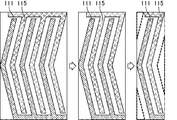
- FIG. 116 is a schematic plan view showing an example of electrode arrangement of a conventional IPS mode liquid crystal display device.
- a pixel electrode 111 and a common electrode 115 are arranged in one pixel, and each of them is a bent (V-shaped) comb.
- V-shaped bent
- the wide viewing angle characteristic can be obtained by arranging the longitudinal directions of the comb teeth of the electrodes 111 and 115 to be oblique with respect to the wirings.
- the pixel size is sufficiently large, even if a dark region occurs in some part, it is possible to obtain a bright display as a whole by supplementing the brightness in other regions, but as the pixel size decreases, Since the ratio of the area occupied by the dark region to the entire pixel becomes large, the influence of a decrease in transmittance appears more remarkably when the pixel has a higher definition.
- the present invention has been made in view of the above situation, and an object of the present invention is to provide a liquid crystal display device capable of achieving both high transmittance and wide viewing angle characteristics even when the pixel size is reduced. Is.
- the present inventors paid attention to the structure of the pixel electrode and the common electrode.
- simply changing the shape of the comb teeth of the pixel electrode and the common electrode has a high transmittance and a wide viewing angle characteristic. Judging that balancing is difficult.
- linear electrodes are arranged on the substrate on the opposite side through the liquid crystal layer along one linear electrode of the pair of linear electrodes.
- the present inventors have found that when a voltage is applied, liquid crystal molecules can be aligned in a plurality of directions to obtain wide viewing angle characteristics and high transmittance can be secured.
- one aspect of the present invention includes a first substrate, a second substrate, and a liquid crystal layer sandwiched between the first substrate and the second substrate, the first substrate being independent from each other.
- the first linear electrode and the second linear electrode included in each of the two electrode pairs adjacent to each other include a plurality of electrode pairs each including the linear electrode and the second linear electrode.
- a straight line passing between the pair is arranged so as to be symmetrical with respect to each other with respect to the reference axis, and the linear electrode located farther from the reference axis is the first linear electrode, The linear electrode closer to the reference axis is the second linear electrode, and the second substrate is formed along the first linear electrode or the second linear electrode.
- a liquid crystal display device having a third linear electrode.
- the liquid crystal display device includes a first substrate, a second substrate, and a liquid crystal layer sandwiched between the first substrate and the second substrate.
- the first substrate has a plurality of electrode pairs including a first linear electrode and a second linear electrode that are independent from each other, and the second substrate has a third linear electrode.
- An electric field is formed in the liquid crystal layer based on the potential difference between the first to third linear electrodes. Then, the orientation of the liquid crystal molecules changes according to the strength of the electric field, the amount of light transmission is adjusted, and the on / off of the display is adjusted.
- the magnitude of the potential supplied to the first to third linear electrodes is not particularly limited and can be appropriately adjusted depending on the design.
- the first linear electrode and the second linear electrode respectively included in two adjacent electrode pairs are straight lines passing between the electrode pairs.
- the linear electrode at a position farther from the axis serving as a reference for the line symmetry is the “first linear electrode”, and the linear electrode at a closer position is the “second linear electrode”. is there.
- Signals having the same potential are supplied to the first linear electrodes and the second linear electrodes respectively included in two adjacent electrode pairs.
- the third linear electrode is formed along the first linear electrode or the second linear electrode. Therefore, since a constant electric field can be partitioned between the third linear electrode and the first linear electrode or the second linear electrode, the alignment controllability of liquid crystal molecules is increased. Display performance (transmittance, viewing angle characteristics, etc.) is stable.
- the configuration of the liquid crystal display device is not particularly limited by other components as long as such components are essential.
- an electrode different from the first to third linear electrodes for example, fourth, fifth and subsequent electrodes
- the other electrode is a linear electrode. May not be a linear electrode.
- the potential supplied to the third linear electrode is applied to the first or second linear electrode formed along the third linear electrode. It is preferably the same as the supplied potential. Thereby, since the wall used as a reference potential can be formed between the first or second linear electrode and the third linear electrode, the display performance is stabilized.
- the potential supplied to the third linear electrode and the potential supplied to the first linear electrode or the second linear electrode are common potentials. Thereby, it becomes easier to form a wall having a reference potential.
- electrically connecting the third linear electrode and the first or second linear electrode to each other through, for example, an external wiring these potentials become the same.
- the means for electrically connecting the third linear electrode and the first or second linear electrode is not particularly limited.
- the third linear electrode is a linear electrode located farther from the axis serving as the reference for the line symmetry, that is, the first linear electrode. It is preferably formed along the electrodes.
- the first linear electrode and the second linear electrode are preferably arranged on the same layer. Even when the first linear electrode and the second linear electrode are formed on different layers, it is possible to form a horizontal electric field, but the vertical component is partially included In fact, an oblique electric field is formed. In this case, some liquid crystal molecules may rotate obliquely according to the electric field, thereby reducing the transmittance and viewing angle characteristics. By arranging the first linear electrode and the second linear electrode on the same layer, it becomes difficult to form an electric field of such an oblique component, so that a more uniform lateral electric field can be formed. It is possible to prevent a decrease in transmittance and viewing angle characteristics.
- the liquid crystal display device preferably further includes a scanning signal line passing between the second linear electrodes of the two electrode pairs adjacent to each other.
- the region between the second linear electrodes included in the two electrode pairs adjacent to each other cannot be used as a display because no potential difference occurs. Therefore, an efficient configuration can be obtained by arranging scanning signal lines using this region.
- the liquid crystal display device preferably further includes a switching element connected to each of the second linear electrodes of the two electrode pairs adjacent to each other. Since these two second linear electrodes are supplied with the same potential, this provides an efficient configuration. In particular, when the pixel size is reduced, the effect is great because the size of the switching element is directly linked to the size of the aperture ratio.
- the first substrate further includes a first polarizing plate
- the second substrate further includes a second polarizing plate, the polarization axis of the first polarizing plate, and the second polarizing plate
- the first linear electrode is arranged so as to be parallel or perpendicular to the polarization axis of the first polarizing plate and the polarization axis of the second polarizing plate
- the second linear electrode is preferably disposed so as to be parallel or orthogonal to the polarization axis of the first polarizing plate and the polarization axis of the second polarizing plate. That is, in this embodiment, the first polarizing plate and the second polarizing plate are in a crossed Nicols arrangement relationship with each other. Since the first linear electrode and the second linear electrode can form a uniform electric field between them, each polarizing plate is parallel or orthogonal to the direction of the electric field. By adjusting the axis, it is possible to obtain good gradation display and white display.
- the length of the first linear electrode and the length of the second linear electrode may be the same or different, but from the viewpoint of making the alignment of the liquid crystal molecules more uniform, they are the same. It is preferable that
- the first linear electrode and the first linear electrode Two ends of each of the two linear electrodes that are close to each other, a side of the first linear electrode that is closer to the second linear electrode, and the second line
- the shape of the region surrounded by the side of the electrode that is close to the first linear electrode is a rectangle, and the aspect ratio of the rectangle is preferably 0.75 or more and less than 1.00.
- the first and second linear electrodes are Two lines vertically lowered from the respective ends of the shorter linear electrode toward the longer linear electrode, and the second linear electrode of the first linear electrode.
- the region surrounded by the side closer to the first linear electrode and the side closer to the first linear electrode of the second linear electrode is a rectangle, and the aspect ratio of the rectangle is 0.75. As mentioned above, it is preferable that it is less than 1.00.
- the viewing angle characteristics obtained differ depending on the shape of a certain range of regions virtually formed by the first linear electrode and the second linear electrode.
- the design that provides the best viewing angle characteristics is when the shape of the region is square, that is, when the aspect ratio of the shape of the region is 1: 1. As the aspect ratio moves away from 1.00, the viewing angle characteristic gradually decreases. However, if the aspect ratio is 0.75 or more, a sufficiently good viewing angle characteristic can be obtained even when the pixel is downsized.
- the term “rectangular” or “square” refers to a shape that can recognize four sides that are substantially orthogonal or parallel to each other, and may have minute irregularities formed in part. .
- liquid crystal display device capable of achieving both high transmittance and wide viewing angle characteristics even when the pixel size is reduced.
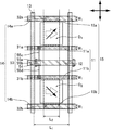
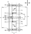
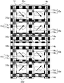
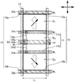
- FIG. 3 is a schematic plan view of a TFT substrate of the liquid crystal display device of Embodiment 1.
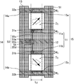
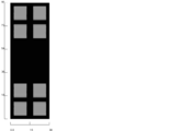
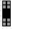
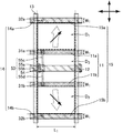
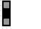
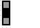
- FIG. 3 is a schematic plan view of a counter substrate of the liquid crystal display device of Embodiment 1.
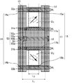
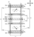
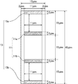
- FIG. 3 is a schematic plan view in which the position of a black matrix is added to the schematic plan view of the TFT substrate of Embodiment 1.
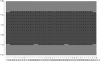
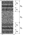
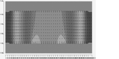
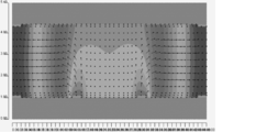
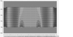
- It is a simulation image which shows the behavior of the liquid crystal molecule in Example 1, and represents the cross-sectional image at the time of no voltage application (0V).
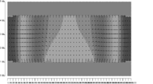
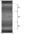
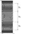
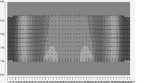
- Example 1 It is a simulation image which shows the behavior of the liquid crystal molecule in Example 1, and represents the planar image at the time of no voltage application (0V). It is a simulation image which shows the behavior of the liquid crystal molecule in Example 1, and represents the cross-sectional image at the time of white voltage application (5.5V). It is a simulation image which shows the behavior of the liquid crystal molecule in Example 1, and represents the planar image at the time of white voltage application (5.5V).
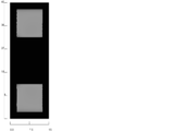
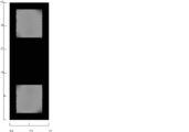
- it is the plane image which represented the light transmittance with the monochrome gradation.
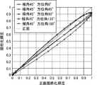
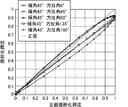
- it is a graph showing each brightness
- FIG. 6 is a schematic plan view of a TFT substrate of a liquid crystal display device of Embodiment 2.
- FIG. 6 is a schematic plan view in which the position of a black matrix is added to the schematic plan view of the TFT substrate of Embodiment 2.
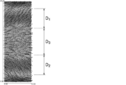
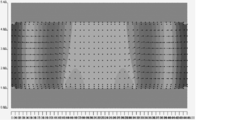
- FIG. 6 is a simulation plane image showing the behavior of liquid crystal molecules in Example 2. In Example 2, it is the plane image which represented the light transmittance with the monochrome gradation.
- 6 is a schematic plan view of a TFT substrate of a liquid crystal display device according to Embodiment 3.
- FIG. 6 is a schematic plan view in which the position of a black matrix is added to the schematic plan view of the TFT substrate of Embodiment 3.
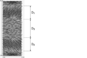
- FIG. 6 is a simulation plane image showing the behavior of liquid crystal molecules in Example 3.
- Example 3 it is the plane image which represented the light transmittance with the monochrome gradation.
- 6 is a schematic plan view of a TFT substrate of a liquid crystal display device of Embodiment 4.
- FIG. 6 is a schematic plan view in which the position of a black matrix is added to the schematic plan view of a TFT substrate of Embodiment 4.
- FIG. 6 is a simulation plane image showing the behavior of liquid crystal molecules in Example 4.
- 6 is a schematic plan view of a TFT substrate of a liquid crystal display device of Embodiment 5.
- 10 is a schematic plan view in which the position of a black matrix is added to the schematic plan view of the TFT substrate of Embodiment 5.
- 10 is a simulation plane image showing the behavior of liquid crystal molecules in Example 5.
- it is the plane image which represented the light transmittance with the monochrome gradation.
- 7 is a schematic plan view of a TFT substrate of a liquid crystal display device according to Embodiment 6.
- FIG. 10 is a schematic plan view in which the position of a black matrix is added to the schematic plan view of the TFT substrate of Embodiment 6.
- 10 is a simulation plane image showing the behavior of liquid crystal molecules in Example 6.
- Example 6 it is the plane image which represented the light transmittance with the monochrome gradation.
- FIG. 10 is a schematic plan view of a TFT substrate of a liquid crystal display device according to a seventh embodiment.
- FIG. 10 is a schematic plan view of a TFT substrate of a liquid crystal display device of a preferred example of Embodiment 7.
- FIG. 5 is a schematic diagram illustrating a configuration of a pixel serving as a reference (Ref) for each sample in evaluation tests 1 to 5, and represents a TFT substrate side.
- FIG. 5 is a schematic diagram illustrating a configuration of a pixel that serves as a reference (Ref) for each sample in evaluation tests 1 to 5, and represents a counter substrate side.
- It is a simulation image (planar image) which shows the behavior of a liquid crystal molecule at the time of white voltage application (5.5V) in sample A.
- the light transmittance is a flat image in monochrome gradation. It is a graph showing each brightness
- Sample I it is a planar image in which light transmittance is expressed in monochrome gradation. It is a graph showing each brightness
- the light transmittance is a flat image representing monochrome gradation.
- 6 is a simulation image (planar image) showing the behavior of liquid crystal molecules when white voltage is applied to Sample N (7.0 V).
- 6 is a simulation image (cross-sectional image) showing the behavior of liquid crystal molecules when white voltage is applied to Sample N (7.0 V).
- the light transmittance is a flat image representing monochrome gradation. It is a graph showing each brightness
- the light transmittance is a flat image representing monochrome gradation. It is a graph showing each brightness
- the light transmittance is a flat image representing monochrome gradation.
- FIG. 6 is a simulation image (planar image) showing the behavior of liquid crystal molecules when white voltage is applied (3.2 V) in sample W.
- FIG. 4 is a simulation image (cross-sectional image) showing the behavior of liquid crystal molecules when white voltage is applied (3.2 V) in sample W.
- the light transmittance is a flat image representing monochrome gradation. It is a graph showing each brightness
- FIG. 6 is a simulation image (planar image) showing the behavior of liquid crystal molecules when white voltage is applied (2.7 V) in Sample X.
- FIG. 4 is a simulation image (cross-sectional image) showing the behavior of liquid crystal molecules when white voltage is applied (2.7 V) in Sample X.
- FIG. In Sample X the light transmittance is a flat image representing monochrome gradation. It is a graph showing each brightness
- liquid crystal display devices of the following first to seventh embodiments can be applied to televisions, personal computers, mobile phones, car navigation systems, information displays, and the like.
- a region in which the orientation of liquid crystal molecules is controlled by a pixel electrode controlled by one switching element and a common electrode facing the pixel electrode is defined as one “pixel”.
- the orientation of liquid crystal molecules is controlled by each of the plurality of pixel electrodes and each of the common electrodes facing each of the plurality of pixel electrodes. The entire area becomes one “pixel”.
- the effect of the present invention is prominent when the pixel size is small.
- the present invention may be applied when the pixel size is large as in the fifth or sixth embodiment described later.
- the pixel size there is a case where at least one side of the pixel is 20 ⁇ m or less, and further, 17 ⁇ m or less.
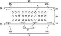
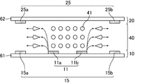
- Embodiment 1 1 and 2 are schematic cross-sectional views of the liquid crystal display device of Embodiment 1.
- FIG. FIG. 1 shows the time when no voltage is applied
- FIG. 2 shows the time when a white voltage is applied.
- the liquid crystal display device of Embodiment 1 includes a TFT substrate (first substrate) 10, a counter substrate (second substrate) 20, and a liquid crystal layer 40 sandwiched between the TFT substrate 10 and the counter substrate 20.
- the liquid crystal layer 40 contains liquid crystal molecules 41 having positive dielectric anisotropy, and the liquid crystal molecules 41 are horizontal to the surfaces of the substrates 10 and 20 when no voltage is applied and when a voltage is applied. Oriented in various directions.
- the TFT substrate 10 includes a support substrate 61, a TFT (switching element), a scanning signal line, a data signal line, a common signal line, a pixel electrode (second linear electrode) 11, and a TFT common electrode (first linear electrode). 15, an insulating film, an alignment film, and the like that separate the pixel electrode 11 and the TFT common electrode 15 into different layers.
- the counter substrate 20 includes a support substrate 62, a color filter, a black matrix, a counter common electrode (third linear electrode) 25, an alignment film, and the like.
- the pixel electrode 11 and the TFT common electrode 15 are independent from each other, and signals having different potentials are supplied thereto. Thereby, a voltage can be applied in the liquid crystal layer 40.
- the pixel electrode 11 is further divided into a first pixel electrode 11a and a second pixel electrode 11b.
- the first pixel electrode 11a and the second pixel electrode 11b are arranged on the same layer, and an image signal (pixel potential) having the same potential is supplied to each of them.
- one TFT 53 is connected to each of the first pixel electrode 11a and the second pixel electrode 11b.
- the first pixel electrode 11a and the second pixel electrode 11b may or may not be connected to each other by a member other than the TFT.
- the TFT common electrode 15 is a common electrode provided on the TFT substrate 10 side, and is further divided into a first TFT common electrode 15a and a second TFT common electrode 15b.
- the first TFT common electrode 15a and the second TFT common electrode 15b are disposed on the same layer, and a common signal having the same potential is supplied to each of them.
- the first TFT common electrode 15a and the second TFT common electrode 15b may or may not be connected to each other by other members.
- the first pixel electrode 11a, the second pixel electrode 11b, the first TFT common electrode 15a, and the second TFT common electrode 15b are all disposed on the same layer. As a result, an electric field having an oblique component with respect to the substrate surface is hardly formed, so that a uniform lateral electric field can be formed, and deterioration of transmittance and viewing angle characteristics can be prevented.
- Examples of the member positioned in the lower layer include an insulating film formed on the support substrate 61.
- the insulating film may be formed of an organic material or an inorganic material, and may be a single film. There may be a plurality of films.
- the counter common electrode 25 is a common electrode provided on the counter substrate 20 side, and is further divided into a first counter common electrode 25a and a second counter common electrode 25b.
- the first counter common electrode 25a and the second counter common electrode 25b are electrodes arranged on the same layer, and a common signal having the same potential is supplied to each of them.
- the first counter common electrode 25a and the second counter common electrode 25b may be connected to each other through wiring provided inside or outside the counter substrate 20, or may not be connected to each other.
- the counter common electrode 25 is disposed along the TFT common electrode 15 with the liquid crystal layer 40 interposed therebetween, that is, the TFT common electrode 15 and the counter common electrode 25 are disposed so as to overlap each other with the liquid crystal layer 40 interposed therebetween. ing. Further, a common signal (common potential) having the same potential is supplied to the TFT common electrode 15 and the counter common electrode 25. Thereby, a wall of a reference potential that virtually serves as a partition for partitioning the liquid crystal layer 40 into a plurality of regions can be formed. For example, the TFT common electrode 15 and the counter common electrode 25 may or may not be electrically connected to each other via an external wiring.
- a polarizing plate On the surface of the TFT substrate 10 opposite to the liquid crystal layer 40 side, a polarizing plate (first polarizing plate) is attached. A polarizing plate (second polarizing plate) is attached to the surface of the counter substrate 20 opposite to the liquid crystal layer 40 side.
- the first polarizing plate attached on the surface of the TFT substrate 10 and the second polarizing plate attached on the surface of the counter substrate 20 are arranged so that their polarization axes are orthogonal to each other. Yes. Further, the first polarizing plate and the second polarizing plate have respective polarization axes that are common to the first pixel electrode 11a, the second pixel electrode 11b, the first TFT common electrode 15a, and the second TFT. It arrange
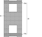
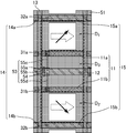
- FIG. 3 to 5 are schematic plan views of the liquid crystal display device according to the first embodiment.
- FIG. 3 is a schematic plan view of the TFT substrate
- FIG. 4 is a schematic plan view of the counter substrate.
- FIG. 5 is obtained by adding the position of the black matrix to the schematic plan view of the TFT substrate.
- the scanning signal lines 12 and the data signal lines 13 are arranged so as to cross each other. Near the contact point between the scanning signal line 12 and the data signal line 13, a TFT (thin film transistor) 53 is provided.
- a common signal line 14 extending in parallel with the scanning signal line 12 is provided between the scanning signal lines 12.
- the term “parallel” used for the electrodes and the wiring includes those that can be said to be substantially parallel, and specifically includes those having an error of 7.5 ° or less.
- the double-headed arrow in FIG. 3 represents the direction of the polarization axis of the polarizing plate.
- the TFT 53 is a switching element including a semiconductor layer 54, a gate electrode 55a, a source electrode 55b, a first drain electrode 55c, and a second drain electrode 55d.
- a part of the scanning signal line 12 is used as it is for the gate electrode 55a.
- the source electrode 55 b is branched from the data signal line 13.
- the drain electrode is divided into a first drain electrode 55c extended toward the first pixel electrode 11a and a second drain electrode 55d extended toward the second pixel electrode 11b.
- the first drain electrode 55c is formed wide at a position overlapping the first pixel electrode 11a, and is connected to the first pixel electrode 11 via a first contact portion 31a penetrating the insulating film. .
- the second drain electrode 55d is formed wide at a position overlapping the second pixel electrode 11b, and is connected to the second pixel electrode via a second contact portion 31b penetrating the insulating film.
- the gate electrode 55a and the semiconductor layer 54 overlap each other with a gate insulating film interposed therebetween.
- the source electrode 55b is connected to the drain electrodes 55c and 55d through the semiconductor layer 54, and the amount of current flowing through the semiconductor layer 54 is adjusted by the scanning signal input to the gate electrode through the scanning signal line 12, and the data signal Transmission of image signals inputted in order of the source electrode 55b, the semiconductor layer 54, the first drain electrode 55c or the first drain electrode 55d, and the first pixel electrode 11a or the second pixel electrode 11b through the line 13 is performed. Be controlled.
- the first pixel electrode 11a and the second pixel electrode 11b are both linear and parallel to each other.
- the scanning signal line 12 is formed in parallel with each of the first pixel electrode 11a and the second pixel electrode 11b and between the first pixel electrode 11a and the second pixel electrode 11b.
- the first TFT common electrode 15a and the second TFT common electrode 15b are both linear and parallel to each other.
- the first TFT common electrode 15a is arranged in parallel to the first common signal line 14a and so as to overlap each other via an insulating film.
- the first TFT common electrode 15a is connected to the first common signal line 14a through a first contact portion 32a penetrating the insulating film.
- the second TFT common electrode 15b is arranged so as to be parallel to the second common signal line 14b and to overlap each other via an insulating film.
- the second TFT common electrode 15b is connected to the second common signal line 14b through a second contact portion 32b penetrating the insulating film.
- the first common signal line 14a and the second common signal line 14b may be connected to each other through, for example, a common bus line, but are connected to each other as long as the same potential is supplied. It does not have to be. In the first embodiment, it is not always necessary to provide a common signal line separately from the TFT common electrode. For example, each of the first TFT common electrode and the second TFT common electrode may be long regardless of the pixel boundary. It may be stretched.
- the first counter common electrode 25a and the second counter common electrode 25b are both linear and parallel to each other. No common signal line is provided on the counter substrate 20 side, and each of the first counter common electrode 25a and the second counter common electrode 25b itself is extended long regardless of the boundary of the first pixel. Yes.
- a separate signal line may be provided separately from the above.
- the combination of the first pixel electrode 11a and the first TFT common electrode 15a and the combination of the second pixel electrode 11b and the second TFT common electrode 15b are each a pair of electrode pairs.
- a plurality of such electrode pairs are formed on the TFT substrate 10.
- a straight line that is parallel to the first pixel electrode 11a and the second pixel electrode 11b and passes between the first pixel electrode 11a and the second pixel electrode 11b is a reference axis.
- the arrangement of the first pixel electrode 11a, the second pixel electrode 11b, the first TFT common electrode 15a, and the second TFT common electrode 15b is determined so as to be line-symmetric with each other.
- all of the first pixel electrode 11a, the second pixel electrode 11b, the first TFT common electrode 15a, and the second TFT common electrode 15b have the same length and width. And parallel to each other.
- the length of each of the first pixel electrode 11a, the second pixel electrode 11b, the first TFT common electrode 15a, and the second TFT common electrode 15b varies depending on the size of the set pixel. It is set in the range of 10 to 15 ⁇ m.
- the widths of the first pixel electrode 11a, the second pixel electrode 11b, the first TFT common electrode 15a, and the second TFT common electrode 15b vary depending on the size of the set pixel. It is set in the range of ⁇ 4 ⁇ m.
- the straight line that bisects the first pixel electrode 11a vertically and the straight line that bisects the first TFT common electrode 15a vertically have the same relationship. That is, the combination of the first pixel electrode 11a and the first TFT common electrode 15a has a symmetrical structure with respect to each other about a straight line that bisects the two vertically.
- the straight line that bisects the second pixel electrode 11b vertically and the straight line that bisects the second TFT common electrode 15b vertically use the straight line that bisects these vertically as a reference axis. They are in a mutually consistent relationship.
- the combination of the second pixel electrode 11b and the second TFT common electrode 15b also has a line-symmetric structure with respect to a straight line that bisects them vertically as a reference axis. Furthermore, the straight lines that bisect each of the electrodes vertically coincide with each other. In other words, it can be said that the electrode pair has a line-symmetric structure with respect to a line that bisects each of the electrodes included in the electrode pair perpendicularly.
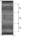
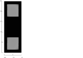
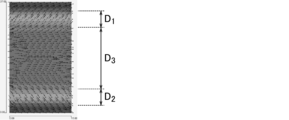
- the black matrix 51 is provided with openings in accordance with regions in which the alignment of liquid crystal molecules is controlled by the respective electrodes. That is, the first pixel electrode 11a, the first TFT common electrode 15a, and regions surrounded by two straight lines that connect the ends of these electrodes close to each other (hereinafter also referred to as the first divided region D1). ), And the second pixel electrode 11b, the second TFT common electrode 15b, and a region surrounded by two straight lines that connect the ends of these electrodes close to each other (hereinafter referred to as the second pixel electrode 11b).
- the black matrix 51 is formed so that the outer edge of the opening is formed along the divided region D2.
- the black matrix 51 forms a lattice shape when viewed as a whole.
- the black matrix 51 is covered.
- the plurality of openings formed so as to be surrounded by the black matrix 51 thus serve as a region that transmits display light.
- the lengths L1 of the first pixel electrode 11a, the second pixel electrode 11b, the first TFT common electrode 15a, and the second TFT common electrode 15b are all the same. It is set so that it is slightly larger than one side of the opening formed along these. That is, preferably, the length L1 of each of the first pixel electrode 11a, the second pixel electrode 11b, the first TFT common electrode 15a, and the second TFT common electrode 15b is formed along these. It is equal to or greater than one side of the opening and 110% or less. Note that the widths W1 of the first pixel electrode 11a, the second pixel electrode 11b, the first TFT common electrode 15a, and the second TFT common electrode 15b are all set to be the same.
- the liquid crystal molecules 41 when no voltage is applied, are composed of the first pixel electrode 11a, the second pixel electrode 11b, the first TFT common electrode 15a, and the second TFT. They are oriented substantially parallel to each of the common electrodes 15b (specifically, including an error of 7.5 ° or less). Such alignment of the liquid crystal molecules 41 can be realized, for example, by an alignment film that has been subjected to alignment treatment. 3 and 5, the white dotted arrow indicates the orientation direction (major axis direction) of the liquid crystal molecules when no voltage is applied.
- the liquid crystal molecules 41 are composed of the first pixel electrode 11a, the second pixel electrode 11b, the first TFT common electrode 15a, and The second TFT common electrode 15b is oriented in an oblique direction.
- the angle in the oblique direction varies depending on the magnitude of the voltage applied in the liquid crystal layer 40.
- the black arrow in FIG.3 and FIG.5 has shown the orientation direction (major axis direction) of the liquid crystal molecule at the time of white voltage application.
- both the first divided region D1 and the second divided region D2 have a rectangle or a square. Thereby, excellent transmittance and wide viewing angle characteristics can be obtained.
- Example 1 When a specific simulation was actually performed assuming the liquid crystal display device of Embodiment 1, the following results were obtained (Example 1).
- the simulation conditions of Example 1 were set as follows.
- the pixel size was 15 ⁇ m ⁇ 45 ⁇ m.
- the width per pixel electrode and TFT common electrode was 2 ⁇ m, and the length was 11 ⁇ m.
- the width and length of the counter common electrode were the same as the width and length of the TFT common electrode.
- the distance between the first pixel electrode 11a and the first TFT common electrode 15a and the distance between the second pixel electrode 11b and the second TFT common electrode 15b are both 11 ⁇ m. . That is, the aspect ratio of the first divided area D1 and the second divided area D2 is 1: 1.
- the size of the opening of the black matrix was 10 ⁇ m ⁇ 10 ⁇ m. That is, the aspect ratio of the opening of the black matrix is 1: 1.
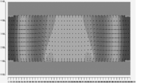
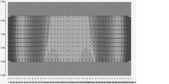
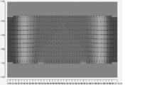
- FIG. 6 to 9 are simulation images showing the behavior of the liquid crystal molecules in Example 1.
- FIG. 6 and 7 show the case when no voltage is applied (0 V)
- FIGS. 8 and 9 show the case when a white voltage is applied (5.5 V).
- 6 and 8 represent cross-sectional images
- FIGS. 7 and 9 represent planar images.
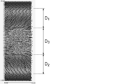
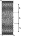
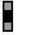
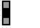
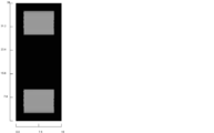
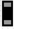
- FIG. 10 is a plane image in which light transmittance is expressed in monochrome gradation in the first embodiment
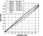
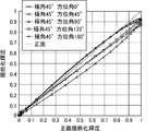
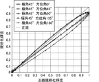
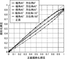
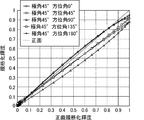
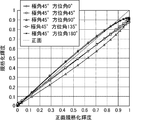
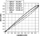
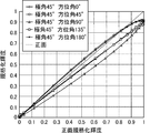
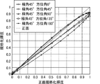
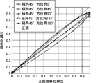
- FIG. 11 is a diagram in which the polar angle is fixed at 45 ° with the display screen as a reference plane in the first embodiment. It is a graph showing each brightness
- the liquid crystal molecules 41 are uniformly aligned in the same direction (a direction parallel to each electrode).
- the liquid crystal molecules 41 located in the region between the first pixel electrode 11a and the second pixel electrode 11b become the first pixel.
- the initial alignment is maintained in the vicinity of the TFT substrate 10 on which the electrode 11a and the second pixel electrode 11b are arranged, but the alignment changes in the vicinity of the counter substrate 20.
- each pixel electrode 11 and common electrodes 15 and 25 opposed thereto (for example, (i) the first TFT common electrode 15a and the first counter common electrode 25a correspond to the first pixel electrode 11a).
- the second pixel electrode 11b corresponds to the second TFT common electrode 15b and the second counter common electrode 25b).
- the electrodes are oriented so as to face an oblique direction.
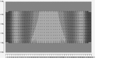
- each region is shown in gradation according to the strength of the electric field. As can be seen from FIG. 8, the region surrounded by the first pixel electrode 11a, the second pixel electrode 11b, and the point of the counter substrate 20 facing the pixel electrodes 11a and 11b is tapered (roughly shaped).
- the electric field distribution is not uniform between the TFT substrate 10 and the counter substrate 20.
- the first pixel electrode 11a, the first TFT common electrode 15a, the first counter common electrode 25a, the region surrounded by the point facing the first pixel electrode of the counter substrate 20, and the first In the region surrounded by the second pixel electrode 11b, the second TFT common electrode 15b, the second counter common electrode 25b, and the point of the counter substrate 20 facing the second pixel electrode 11b the electric field distribution is the TFT substrate. It is uniform between near 10 and near the counter substrate 20, indicating that the potential change is stable.
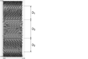
- Most of the liquid crystal molecules 41 included in the enclosed intermediate region D3 are aligned parallel to the electrodes 11a and 11b, and some of the liquid crystal molecules 41 are aligned obliquely to the electrodes 11a and 11b. ing.
- the side of the first pixel electrode 11a on the side close to the first TFT common electrode 15a, the side of the first TFT common electrode 15a on the side close to the first pixel electrode 11a, and the ends thereof are mutually connected.
- the liquid crystal molecules 41 included in the first divided region D1 surrounded by two straight lines connecting the close ones differ in angle depending on the regions, most of them are oriented in a direction of about 45 ° with respect to the electrodes 11a and 15a. Therefore, the change in angle is smooth and uniform.
- the side of the second pixel electrode 11b near the second TFT common electrode 15b, the side of the second TFT common electrode 15b near the second pixel electrode 11b, and the ends of these sides Although the liquid crystal molecules 41 included in the second divided region D2 surrounded by two straight lines that connect each other close to each other have different angles depending on the regions, most of them are in a direction of about 45 ° with respect to the electrodes 11b and 15b. It is oriented and the change in angle is smooth and uniform.
- the characteristic point here is that the alignment distribution (director distribution) of these liquid crystal molecules is a straight line passing between the first pixel electrode 11a and the second pixel electrode 11b, more specifically, The point is that they are symmetrical with respect to each other about a straight line that bisects one pixel.
- two regions including a plurality of liquid crystal molecules having alignment orientations in different directions and having a symmetrical alignment pattern around a certain reference axis can be formed.
- the alignment of the liquid crystal molecules can be made uniform in the portion used as the display region, and two regions having alignment orientations in different directions can be formed. Therefore, it is possible to efficiently use light and obtain excellent viewing angle characteristics.
- the configuration of the first embodiment even if the pixel size is designed to be small, an excellent effect that the characteristics are not deteriorated can be exhibited.
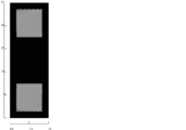
- the transmittance As shown in FIG. 10, it is understood that light is uniformly transmitted through the entire region serving as the opening of the black matrix 51, and a high transmittance can be secured.
- the viewing angle characteristics as shown in FIG. 11, since there is no great difference in luminance depending on the angle, almost uniform display can be obtained regardless of the angle at which the viewing angle is tilted. Recognize.
- the aspect ratio of the first divided area D1 and the second divided area D2 and the aspect ratio of the opening of the black matrix 51 are not necessarily matched as shown in the first embodiment. There is no need.
- the shape of the opening of the black matrix 51 may be determined according to a region suitable for display, and is not limited to a rectangle or a square. Further, the magnitude relationship between the size of the first divided region D1 and the second divided region D2 and the size of the opening of the black matrix 51 is not particularly limited.
- a transparent material such as glass or plastic is preferably used.
- a transparent material such as silicon nitride, silicon oxide, or photosensitive acrylic resin is preferably used.
- a silicon nitride film is formed by a plasma-enhanced chemical vapor deposition (PECVD) method, and a photosensitive acrylic resin film is formed on the silicon nitride film by a die coating (coating) method. It is formed by film formation.
- the holes provided in the insulating film for forming the contact portions 31 and 32 can be formed by performing dry etching (channel etching).
- Various electrodes constituting the scanning signal line 12, the data signal line 13, and the TFT 53 are formed of a single layer or a plurality of layers of a metal such as titanium, chromium, aluminum, molybdenum, or an alloy thereof by a sputtering method or the like.
- the film can be formed and then patterned by photolithography or the like. For these various wirings and electrodes formed on the same layer, the same material is used to make the manufacturing more efficient.
- the semiconductor layer 54 of the TFT 53 for example, a high resistance semiconductor layer (i layer) made of amorphous silicon, polysilicon or the like, and a low resistance semiconductor layer made of n + amorphous silicon or the like in which amorphous silicon is doped with an impurity such as phosphorus or the like ( n + layer), but the can be used as a laminate of, as the other, IGZO (indium - gallium - zinc - oxygen) oxide semiconductor such as is preferably used.
- IGZO indium - gallium - zinc - oxygen
- an oxide semiconductor such as IGZO as the material of the semiconductor layer 54, the electron mobility is high and the size of the TFT can be reduced, so that a large aperture ratio can be secured. Therefore, an oxide semiconductor using IGZO is advantageous when reducing the size of a pixel. In addition, since the off-leakage characteristic is low, the charge can be held for a long time, and the advantage that low frequency driving is possible can be obtained.
- the pixel electrode 11, the TFT common electrode 15, and the counter common electrode 25 are, for example, transparent conductive materials such as indium tin oxide (ITO), indium zinc oxide (IZO), zinc oxide (ZnO), tin oxide (SnO), Alternatively, an alloy of these can be formed into a single layer or a plurality of layers by a sputtering method or the like, and then patterned using a photolithography method or the like.
- a photosensitive resin (color resist) that transmits light corresponding to each color is preferably used.
- the material of the black matrix 51 is not particularly limited as long as it has a light shielding property, and a resin material containing a black pigment or a metal material having a light shielding property is preferably used.
- the color filter and the black matrix 51 may be arranged not on the counter substrate 20 side but on the TFT substrate 10 side.
- the TFT substrate 10 and the counter substrate 20 manufactured in this way are provided with a plurality of columnar spacers made of an insulating material on one substrate, and then bonded to each other using a sealing material.
- a liquid crystal layer 40 is formed between the TFT substrate 10 and the counter substrate 20, but when the dropping method is used, the liquid crystal material is dropped before the substrates are bonded, and the vacuum injection method is used. The liquid crystal material is injected after the substrates are bonded.
- a material having a positive dielectric anisotropy is preferably used.
- a liquid crystal display device is completed by affixing a polarizing plate, retardation film, etc. on the surface on the opposite side to the liquid crystal layer 40 side of each board
- Embodiment 2 In the second embodiment, the length of the pixel electrode and the length of the common electrode facing the pixel electrode (for example, (i) the first TFT common electrode corresponds to the first pixel electrode, and (ii) the second The second TFT common electrode corresponds to the pixel electrode of FIG. 5), but is the same as that of the first embodiment except that each pixel electrode is different.
- the length of the pixel electrode is designed to be larger than the length of the common electrode facing the pixel electrode.
- FIG. 12 is a schematic plan view of the TFT substrate of the liquid crystal display device according to the second embodiment
- FIG. 13 is a diagram in which the position of the black matrix is further added.
- the first pixel electrode 11a and the first TFT common electrode 15a are parallel to each other, but the length of the first pixel electrode 11a is the same as that of the first TFT common electrode 15a. The length is 1.0 to 1.7 times.
- the second pixel electrode 11b and the second TFT common electrode 15b are parallel to each other, but the length of the second pixel electrode 11b is the length of the second TFT common electrode 15b.
- the width of the first pixel electrode 11a, the width of the second pixel electrode 11b, the width of the first TFT common electrode 15a, and the width of the second TFT common electrode 15b are the same.
- the lengths L2 of the first TFT common electrode 15a and the second TFT common electrode 15b are the openings of the black matrix 51 formed along these lengths.
- the length L1 of each of the first pixel electrode 11a and the second pixel electrode 11b and the black matrix 51 respectively formed along these are designed to be shorter than the length of one side. It is designed to be longer than the length of one side of the opening.
- the length of each of the first TFT common electrode 15a and the second TFT common electrode 15b is 0.9 which is the length of one side of the opening of the black matrix 51 formed along these.
- the length of each of the first pixel electrode 11a and the second pixel electrode 11b is .0 times the length of one side of the opening of the black matrix 51 formed along these. 9 to 1.5 times.
- Example 2 When a specific simulation was actually performed assuming the liquid crystal display device of Embodiment 2, the following results were obtained (Example 2).
- the simulation conditions of Example 2 were set as follows.
- the pixel size was 15 ⁇ m ⁇ 45 ⁇ m.
- the width per pixel electrode 11a, 11b was 2 ⁇ m, and the length per pixel electrode 11a, 11b was 15 ⁇ m.
- the width per common electrode 15a, 15b was 2 ⁇ m, and the length per common electrode 15a, 15b was 9 ⁇ m.
- the width and length of the counter common electrode were the same as the width and length of the TFT common electrode.
- the distance between the first pixel electrode 11a and the first TFT common electrode 15a and the distance between the second pixel electrode 11b and the second TFT common electrode 15b are both 11 ⁇ m. . That is, the aspect ratio of the first divided area D1 and the second divided area D2 is 9:11.
- the size of the opening of the black matrix was 10 ⁇ m ⁇ 10 ⁇ m. That is, the aspect ratio of the opening of the black matrix is 1: 1.
- FIG. 14 is a simulation plane image showing the behavior of liquid crystal molecules in Example 2.
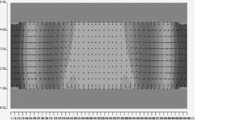
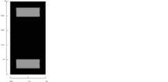
- FIG. 15 is a planar image in which light transmittance is expressed in monochrome gradation in the second embodiment. Based on FIG. 14 and FIG. 15, in the case of Example 2, the orientation distribution of liquid crystal molecules and the transmittance in each opening region were confirmed. As a result, almost the same orientation characteristics as Example 1 were obtained, Since substantially the same transmittance could be obtained, it was confirmed that excellent transmittance and viewing angle characteristics can be obtained also in the second embodiment.
- the length of the pixel electrode and the length of the common electrode facing the pixel electrode (for example, (i) the first TFT common electrode corresponds to the first pixel electrode, and (ii) the second electrode).
- the second TFT common electrode corresponds to the above-mentioned pixel electrode.
- all of them are smaller than the length of each side of the opening of the black matrix formed along these electrodes. Is the same as in the first embodiment.
- the third embodiment is common to the first embodiment in that the length of the pixel electrode is designed to be the same as the length of the common electrode facing the pixel electrode.
- FIG. 16 is a schematic plan view of the TFT substrate of the liquid crystal display device according to the third embodiment
- FIG. 17 is a diagram in which the position of the black matrix is further added.
- the lengths L2 of the first pixel electrode 11a, the second pixel electrode 11b, the first TFT common electrode 15a, and the second TFT common electrode 15b are as follows. Are designed so as to be shorter than the length of one side of the opening of the black matrix 51 formed along each.
- the first pixel electrode 11a, the second pixel electrode 11a, the first TFT common electrode 15a, and the second TFT common electrode 15b have the same length L2 and width W1, respectively. It is 0.7 to 0.9 times the length of one side of the opening of the black matrix 51 formed along each.
- Example 3 When a specific simulation was actually performed assuming the liquid crystal display device of Embodiment 3, the following results were obtained (Example 3).
- the simulation conditions of Example 3 were set as follows.
- the pixel size was 15 ⁇ m ⁇ 45 ⁇ m.
- the width per pixel electrode 11a, 11b and each common electrode 15a, 15b was 2 ⁇ m
- the length per pixel electrode 11a, 11b and each common electrode 15a, 15b was 7 ⁇ m.
- the width and length of the counter common electrode were the same as the width and length of the TFT common electrode.
- the distance between the first pixel electrode 11a and the first TFT common electrode 15a and the distance between the second pixel electrode 11b and the second TFT common electrode 15b are both 11 ⁇ m. . That is, the aspect ratio of the first divided area D1 and the second divided area D2 is 7:11.
- the size of the opening of the black matrix was 10 ⁇ m ⁇ 10 ⁇ m. That is, the aspect ratio of the opening of the
- FIG. 18 is a simulation plane image showing the behavior of liquid crystal molecules in Example 3.
- FIG. 19 is a planar image in which light transmittance is expressed in monochrome gradation in the third embodiment. Based on FIGS. 18 and 19, the alignment distribution of the liquid crystal molecules was confirmed in the case of Example 3. As a result, it was confirmed that substantially the same alignment characteristics as Example 1 could be obtained. In addition, the transmittance is slightly lower in the vicinity of the corner of the opening of the black matrix due to the shortening of each electrode, which is slightly inferior to the first and second embodiments, but is sufficient as display characteristics. High transmittance was obtained. From the above, according to Embodiment 3, it was confirmed that excellent viewing angle characteristics and sufficient transmittance can be obtained.
- Embodiment 4 the width of the pixel electrode and the width of the common electrode facing the pixel electrode (for example, (i) the first TFT common electrode corresponds to the first pixel electrode, and (ii) the second electrode)
- the second TFT common electrode corresponds to the pixel electrode.) Except that the pixel electrodes are different from each other.
- the width of the pixel electrode is designed to be smaller than the width of the common electrode facing it.
- FIG. 20 is a schematic plan view of the TFT substrate of the liquid crystal display device of Embodiment 4, and FIG. 21 is a diagram in which the position of the black matrix is further added.
- the first pixel electrode 11a and the first TFT common electrode 15a are parallel to each other, but the width of the first pixel electrode 11a is the width of the first TFT common electrode 15a. Is 0.75 to 1.0 times greater than
- the second pixel electrode 11b and the second TFT common electrode 15b are parallel to each other, but the width of the second pixel electrode 11b is 0 of the width of the second TFT common electrode 15b. .75 to 1.0 times.
- the first pixel electrode 11a and the second pixel electrode 11b have the same width W1, and the first TFT common electrode 15a and the second TFT common electrode 15b have the same width W2.
- the length L1 of the first pixel electrode 11a, the second pixel electrode 11b, the first TFT common electrode 15a, and the second TFT common electrode 15b is the same.
- the first TFT common electrode 15a and the second TFT common electrode 15b are designed to have a large width. A part of the TFT common electrode 15b slightly extends to the inside of the opening of the black matrix 51 formed along these electrodes.
- Example 4 When a specific simulation was actually performed assuming the liquid crystal display device of Embodiment 4, the following results were obtained (Example 4).
- the simulation conditions of Example 4 were set as follows.
- the pixel size was 15 ⁇ m ⁇ 45 ⁇ m.
- the width per pixel electrode 11a, 11b was 2 ⁇ m, and the length per pixel electrode 11a, 11b was 11 ⁇ m.
- the width per common electrode 15a, 15b was 3 ⁇ m, and the length per common electrode 11a, 11b was 11 ⁇ m.
- the width and length of the counter common electrode were the same as the width and length of the TFT common electrode.
- the distance between the first pixel electrode 11a and the first TFT common electrode 15a and the distance between the second pixel electrode 11b and the second TFT common electrode 15b are both 10 ⁇ m. . That is, the aspect ratio of the first divided region D1 and the second divided region D2 is 11:10.
- the size of the opening of the black matrix was 10 ⁇ m ⁇ 10 ⁇ m. That is, the aspect ratio of the opening of the black matrix is 1: 1.
- FIG. 22 is a simulation plane image showing the behavior of liquid crystal molecules in Example 4.
- FIG. 23 is a planar image in which light transmittance is expressed in monochrome gradation in the fourth embodiment. Based on FIG. 22 and FIG. 23, the alignment distribution of the liquid crystal molecules was confirmed in the case of Example 4, and it was found that substantially the same alignment characteristics as Example 1 could be obtained. Further, with respect to the transmittance, the transmittance spreads slightly along the upper side or the lower side of the opening portion of the black matrix because each electrode extends to the opening portion, which is slightly inferior to the first and second embodiments. However, sufficient transmittance was obtained as display characteristics. From the above, according to Embodiment 4, it was confirmed that excellent viewing angle characteristics and sufficient transmittance can be obtained.
- one pixel is not composed of two electrode pairs composed of a combination of one pixel electrode and one common electrode opposed to the pixel electrode, but two pixel electrodes and one electrode arranged therebetween. Although it differs from Embodiment 1 by the point comprised by the two electrode pairs which consist of a combination of a common electrode, other than that is the same as that of Embodiment 1.
- the fifth embodiment is preferably used when the pixel size is larger than that of the first embodiment.
- FIG. 24 is a schematic plan view of the TFT substrate of the liquid crystal display device according to the fifth embodiment
- FIG. 25 is a diagram in which the position of the black matrix is further added.
- a combination of the first pixel electrode 11a, the first TFT common electrode 15a and the third pixel electrode 11c, and the second pixel electrode 11b, the second TFT common electrode 15b and the fourth pixel electrode Each of the combinations of the pixel electrodes 11d constitutes one electrode pair, and a plurality of such electrode pairs are formed on the TFT substrate.
- the first pixel electrode 11a is further divided into two structural units 11a1 and 11a2, and the first TFT common electrode 15a is further divided into two structural units 15a1 and 15a2.
- the third pixel electrode 11c is further divided into two structural units 11c1 and 11c2.
- the second pixel electrode 11b is further divided into two structural units 11b1 and 11b2, and the second TFT common electrode 15b is further divided into two structural units 15b1 and 15b2.
- the fourth pixel electrode 11d is further divided into two structural units 11d1 and 11d2.
- Each constituent unit 11a1, 11a2 of the first pixel electrode, each constituent unit 11b, 11b2 of the second pixel electrode, each constituent unit 11c1, 11c2 of the third pixel electrode, and each constituent unit of the fourth pixel electrode Each of 11d1 and 11d2 is connected to one TFT 53, and an image signal (pixel potential) having the same potential is supplied to each of them.
- a straight line that is parallel to and passes between the constituent units 11a1 and 11a2 of the first pixel electrode and the constituent units 11b and 11b2 of the second pixel electrode The first pixel electrode constituent units 11a1 and 11a2, the second pixel electrode constituent units 11b1 and 11b2, the third pixel electrode constituent units 11c1 and 11c2, The arrangement of the constituent units 11d1 and 11d2 of the four pixel electrodes, the constituent units 15a1 and 15a2 of the first TFT common electrode, and the constituent units 15b1 and 15b2 of the second TFT common electrode is determined.
- the respective structural units 11a1 and 11a2 of the first pixel electrode, the respective structural units 11b1 and 11b2 of the second pixel electrode, the respective structural units 11c1 and 11c2 of the third pixel electrode, and the fourth pixel electrode are identical length and width. And parallel to each other.
- the black matrix 51 is provided with openings in accordance with regions where the orientation of liquid crystal molecules is controlled by the respective electrodes. That is, the respective structural units 11a1 and 11a2 of the first pixel electrode 11a, the respective structural units 15a1 and 15a2 of the first TFT common electrode 15a, the structural units 11c1 and 11c2 of the third pixel electrode 11c, and the second pixel electrode 11b.
- each divided region configured based on each of the structural units 11b1 and 11b2 of the second TFT common electrode 15b, each of the structural units 15b1 and 15b2 of the second TFT common electrode 15b, and each of the structural units 11d1 and 11d2 of the fourth pixel electrode 11d.
- a black matrix 51 is formed so that the outer edge of the opening is formed along the edge.
- the third divided region D4 and the fourth divided region D5 are configured based on the third divided region D4, the third divided region D4 includes the third sub divided regions d1 and d2, and the fourth divided region D5 includes the fourth sub-divided regions d3 and d4.
- the first divided region D1 and the second divided region D2 are each further divided into four parts, but each sub divided region d1 and d2 per one
- the size is equivalent to each size of the first divided region D1 and the second divided region D2 in the first embodiment.
- the plurality of openings formed in the black matrix 51 in this manner serve as a region that transmits display light.
- Example 5 When a specific simulation was actually performed assuming the liquid crystal display device of Embodiment 5, the following results were obtained (Example 5).
- the simulation conditions of Example 5 were set as follows.
- the pixel size was 30 ⁇ m ⁇ 90 ⁇ m.
- the width of each unit of the pixel electrode and the TFT common electrode was 2 ⁇ m, and the length was 11 ⁇ m.
- the width and length of each constituent unit of the counter common electrode were the same as the width and length of each constituent unit of the TFT common electrode.
- the size of the opening of the black matrix was 10 ⁇ m ⁇ 10 ⁇ m. That is, the aspect ratio of the opening of the black matrix is 1: 1.
- FIG. 26 is a simulation plane image showing the behavior of liquid crystal molecules in Example 5.
- FIG. 27 is a plane image in which light transmittance is expressed in monochrome gradation in the fifth embodiment. 26 the alignment distribution of the liquid crystal molecules in Example 5 was confirmed. As a result, a well-balanced oblique alignment could be obtained as in Example 1, although the alignment distribution of the liquid crystal molecules was different.
- the transmittance in the case of Example 5 was confirmed based on FIG. 27, it was confirmed that uniform transmittance was obtained in each divided region. However, there are many areas that need to be shielded from light by the black matrix, and the transmittance was substantially the same as that of Example 1 with a smaller pixel size. For this reason, even if the pixel size is large, the present invention can be applied, but the result shows that the first embodiment is more efficient in consideration of the light utilization efficiency.
- Embodiment 6 In the sixth embodiment, one pixel is not composed of two electrode pairs composed of a combination of one pixel electrode and one common electrode opposed thereto, but two common electrodes and one arranged between them.
- the second embodiment is the same as the fifth embodiment except that the second embodiment is different from the fifth embodiment in that it is composed of two electrode pairs composed of combinations of pixel electrodes.
- Embodiment 6 is a form in which the position of the pixel electrode and the position of the common electrode in Embodiment 5 are interchanged.
- the sixth embodiment is preferably used when the pixel size is larger than that in the first embodiment.
- FIG. 28 is a schematic plan view of the TFT substrate of the liquid crystal display device of Embodiment 6, and FIG. 29 is a diagram in which the position of the black matrix is further added.
- the combination of the fourth TFT common electrode 15d constitutes one set of electrode pairs, and a plurality of such electrode pairs are formed on the TFT substrate.
- the first TFT common electrode 15a is further divided into two structural units 15a1 and 15a2, and the first pixel electrode 11a is further divided into two structural units 11a1 and 11a2.
- the three TFT common electrodes 15c are further divided into two structural units 15c1 and 15c2.
- the second TFT common electrode 15b is further divided into two structural units 15b1 and 15b2
- the second pixel electrode 11b is further divided into two structural units 11b1 and 11b2.
- the fourth TFT common electrode 15d is further divided into two structural units 15d1 and 15d2.
- Each of the constituent units 11a1 and 11a2 of the first pixel electrode and the constituent units 11b1 and 11b2 of the second pixel electrode are connected to one TFT 53, and each has an image signal having the same potential. (Pixel potential) is supplied.
- a straight line that is parallel to and passes between the constituent units 15a1 and 15a2 of the first TFT common electrode and the constituent units 15b1 and 15b2 of the second TFT common electrode As the reference axis, the constituent units 15a1 and 15a2 of the first TFT common electrode, the constituent units 15b and 15b2 of the second TFT common electrode, and the constituent units of the third TFT common electrode so as to be line-symmetric with each other. 15c1, 15c2, the fourth TFT common electrode constituent units 15d1, 15d2, the first pixel electrode constituent units 11a1, 11a2, and the second pixel electrode constituent units 11b1, 11b2 are determined. ing.
- the same length and width are the same for each of the structural units 15d1 and 15d2 of the TFT common electrode, the structural units 11a1 and 11a2 of the first pixel electrode, and the structural units 11b1 and 11b2 of the second pixel electrode. And parallel to each other.
- the black matrix 51 is provided with openings in accordance with regions where the orientation of liquid crystal molecules is controlled by the respective electrodes. That is, the respective structural units 15a1 and 15a2 of the first TFT common electrode, the respective structural units 15b and 15b2 of the second TFT common electrode, the respective structural units 15c1 and 15c2 of the third TFT common electrode, and the fourth TFT common electrode Opening along each divided region configured on the basis of each of the structural units 15d1, 15d2, each of the structural units 11a1, 11a2 of the first pixel electrode, and each of the structural units 11b1, 11b2 of the second pixel electrode
- the black matrix 51 is formed so that the outer edge of the part is formed.
- the third divided region D4 and the fourth divided region D5 are configured based on the fourth TFT common electrode 15d, and the third divided region D4 includes the third sub-divided regions d1 and d2.
- the fourth divided region D5 includes the fourth sub divided regions d3 and d4.
- the first divided region D1 and the second divided region D2 are each configured to be further divided into four, but the size of each divided region is It is equivalent to each size of the 1st division area D1 and the 2nd division area D2 in form 1.
- the plurality of openings formed in the black matrix 51 in this manner serve as a region that transmits display light.
- Example 6 When a specific simulation was actually performed assuming the liquid crystal display device of Embodiment 6, the following results were obtained (Example 6).
- the conditions for the simulation of Example 6 were set as follows.
- the pixel size was 30 ⁇ m ⁇ 90 ⁇ m.
- the width of each unit of the pixel electrode and the TFT common electrode was 2 ⁇ m, and the length was 11 ⁇ m.
- the width and length of each constituent unit of the counter common electrode were the same as the width and length of each constituent unit of the TFT common electrode.
- the size of the opening of the black matrix was 10 ⁇ m ⁇ 10 ⁇ m. That is, the aspect ratio of the opening of the black matrix is 1: 1.
- Embodiment 7 is the same as Embodiment 1 except that the liquid crystal layer contains liquid crystal molecules having negative dielectric anisotropy and the initial alignment orientation of the liquid crystal molecules is different.
- FIG. 32 is a schematic plan view of a TFT substrate of the liquid crystal display device according to the seventh embodiment. As shown in FIG. 32, in the seventh embodiment, each component of the liquid crystal display device including various electrodes and the arrangement thereof are the same as those in the first embodiment.
- the liquid crystal molecules when no voltage is applied, are the first pixel electrode 11a, the second pixel electrode 11b, the first TFT common electrode 15a, and the second TFT common electrode 15b. They are oriented so as to be substantially orthogonal to each other (specifically, including an error of 7.5 ° or less). Further, a region D1 sandwiched between the first pixel electrode 11a and the first TFT common electrode 15a and a region D2 sandwiched between the second pixel electrode 11b and the second TFT common electrode 15b The initial alignment orientation of the liquid crystal molecules contained in each region is substantially the reverse direction (specifically, including an error of 15.0 ° or less). Such alignment of liquid crystal molecules can be realized by, for example, an alignment film that has been subjected to alignment treatment. Note that white dotted arrows in FIG. 32 indicate the orientation direction (major axis direction) of the liquid crystal molecules when no voltage is applied.
- the liquid crystal molecules are the first pixel electrode 11a, the second pixel electrode 11b, the first TFT common electrode 15a, and the second TFT. It is oriented in an oblique direction with respect to each of the common electrodes 15b. The angle in the oblique direction varies depending on the magnitude of the voltage applied in the liquid crystal layer. Note that black arrows in FIG. 32 indicate the orientation direction (major axis direction) of the liquid crystal molecules when a white voltage is applied.
- both the first divided region D1 and the second divided region D2 have a rectangle or a square. Thereby, excellent transmittance and wide viewing angle characteristics can be obtained.
- FIG. 33 is a schematic plan view of a TFT substrate of a liquid crystal display device of a preferred example of Embodiment 7.
- the initial alignment direction of the liquid crystal molecules is set to the first pixel electrode 11a, the second pixel electrode 11b, the first TFT common electrode 15a, and the second TFT common electrode. It is preferable that the tilt angle is 5 to 7 ° without being completely orthogonal to each of 15b.
- the liquid crystal molecules included in the region D1 sandwiched between the first pixel electrode 11a and the first TFT common electrode 15a and the second pixel electrode 11b and the second TFT common electrode 15b are sandwiched.
- the liquid crystal molecules included in the region D2 to be tilted are preferably inclined by 5 to 7 ° in the same direction.
- the liquid crystal molecules included in the regions D1 and D2 are uniformly aligned in the direction of the black arrow in FIG. 33 when a voltage higher than the threshold is applied. Thereby, more excellent display characteristics can be obtained.
- Evaluation test 1 When viewed in plan, verification of transmittance and viewing angle characteristics for different aspect ratios of regions D1 and D2 sandwiched between a pair of linear electrodes independent of each other (more specifically, a pixel electrode and a TFT common electrode) Results are shown.
- the sample B having an aspect ratio of 9:11
- the sample C having an aspect ratio of 7:11
- Sample D and sample E with an aspect ratio of 3:11 were prepared.
- the aspect ratio was adjusted by adjusting the length of the pixel electrode (second linear electrode).
- the width of the pixel electrode is 2 ⁇ m.
- Samples A to E have the same size per pixel, and the width is 15 ⁇ m and the length is 45 ⁇ m.
- the size per TFT in Samples A to E is the same. Samples A to E use the same liquid crystal material.
- the TFT common electrode (first linear electrode) and the counter common electrode (third linear electrode) each have a width of 2 ⁇ m and a length of 11 ⁇ m.
- the counter common electrode is disposed at a position overlapping the TFT common electrode.
- the length of the pixel electrode is 11 ⁇ m for sample A, 9 ⁇ m for sample B, 7 ⁇ m for sample C, 5 ⁇ m for sample D, and 3 ⁇ m for sample E.
- the shape of the opening of the black matrix is a square, and the length of one side is 10 ⁇ m.
- FIG. 34 and FIG. 35 are schematic diagrams showing the configuration of a sample pixel serving as a reference (Ref) in evaluation test 1 and evaluation tests 2 to 5 described later.
- FIG. 34 shows the TFT substrate side.
- Reference numeral 35 denotes the counter substrate side.
- the sample serving as the reference (Ref) matches the following samples A, F, J, and T.
- FIG. 36 and 37 are simulation images showing the behavior of liquid crystal molecules when white voltage is applied (5.5 V) in Sample A, FIG. 36 shows a planar image, and FIG. 37 shows a cross-sectional image.
- FIG. 38 is a plane image in which light transmittance is expressed in monochrome gradation.
- FIG. 39 is a graph when the polar angle is fixed at 45 ° and the azimuth value is changed with the display screen as a reference plane. It is a graph showing each brightness
- FIG. 40 and 41 are simulation images showing the behavior of liquid crystal molecules when white voltage is applied (5.7 V) in sample B, FIG. 40 shows a planar image, and FIG. 41 shows a cross-sectional image.
- FIG. 42 is a plane image in which light transmittance is expressed in monochrome gradation.
- FIG. 43 shows a case where the polar angle is fixed at 45 ° and the value of the azimuth is changed with the display screen as a reference plane. It is a graph showing each brightness
- FIG. 44 and 45 are simulation images showing the behavior of liquid crystal molecules when white voltage is applied (5.9 V) in Sample C, FIG. 44 shows a planar image, and FIG. 45 shows a cross-sectional image.
- FIG. 46 is a plane image in which light transmittance is expressed in monochrome gradation.
- FIG. 47 shows a case where the polar angle is fixed at 45 ° and the value of the azimuth is changed with the display screen as a reference plane. It is a graph showing each brightness
- FIG. 48 and 49 are simulation images showing the behavior of liquid crystal molecules when white voltage is applied (6.2 V) in Sample D, FIG. 48 shows a planar image, and FIG. 49 shows a cross-sectional image.
- FIG. 50 is a plane image in which light transmittance is expressed in monochrome gradation.
- FIG. 51 shows a case where the polar angle is fixed at 45 ° and the value of the azimuth is changed with the display screen as a reference plane. It is a graph showing each brightness
- FIG. 52 and 53 are simulation images showing the behavior of liquid crystal molecules when white voltage is applied (6.7 V) in Sample E, FIG. 52 shows a planar image, and FIG. 53 shows a cross-sectional image.
- FIG. 54 is a plane image showing the light transmittance in monochrome gradation.
- FIG. 55 is a diagram when the polar angle is fixed at 45 ° with the display screen as a reference plane and the value of the azimuth is changed. It is a graph showing each brightness
- the sample D is further disturbed by the boundary line between the divided region D1 and the other region and the boundary line between the divided region D2 and the other region as compared with the samples A to C.
- the boundary lines of different electric fields are not perpendicular to the normal direction of the substrate surface near the respective boundaries as shown in FIG. It has a swelled composition.
- the strength of the electric field is the same as that of Samples A to C in that it gradually changes from the pixel electrode toward the TFT common electrode, and there is no great disturbance in the alignment of the liquid crystal.
- the transmittance as shown in FIG.
- the transmittance is reduced in the vicinity of the pixel electrode, but it is a part of the opening as a whole, and it can be said that the transmittance is sufficiently secured as a whole.
- the viewing angle characteristics as shown in FIG. 51, since there is no great difference in luminance depending on the angle, it can be said that almost uniform display is obtained no matter what angle the viewing angle is tilted.
- the sample E is further disturbed by the boundary line between the divided region D1 and the other region and the boundary line between the divided region D2 and the other region as compared with the samples A to D.
- the boundary lines of different electric fields are not perpendicular to the normal direction of the substrate surface in the vicinity of each boundary, and further toward the TFT common electrode.
- the composition is swelled.
- the strength of the electric field is the same as that of Samples A to D in that it gradually changes from the pixel electrode to the TFT common electrode, and there is no great disturbance in the alignment of the liquid crystal.
- the transmittance as shown in FIG.
- the transmittance is reduced in the vicinity of the pixel electrode, and its area is larger than that of the sample C, but it can be said that the transmittance can be secured as a whole.
- the viewing angle characteristics as shown in FIG. 55, since there is no great difference in luminance depending on the angle, it can be said that almost uniform display is obtained regardless of the viewing angle.
- the aspect ratio is preferably close to 1. .
- the aspect ratio is preferably 1/5 or more, more preferably 1/3 or more, further preferably 7/15 or more, and extremely preferably 3/5 or more. preferable.
- it is preferably 11/15 or more, but if the transmittance is 3/5 or more, it is sufficiently excellent without much difference.
- the viewing angle characteristics were good regardless of the aspect ratio.
- Evaluation test 2 When viewed in plan, verification of transmittance and viewing angle characteristics for different aspect ratios of regions D1 and D2 sandwiched between a pair of linear electrodes independent of each other (more specifically, a pixel electrode and a TFT common electrode) Results are shown.
- Four samples of 11 samples I were prepared. The aspect ratio was adjusted by adjusting the lengths of the TFT common electrode (first linear electrode) and the counter common electrode (third linear electrode).
- Samples F to I have the same size per pixel, 15 ⁇ m in width and 45 ⁇ m in length. The size of each TFT in the samples F to I is the same. Samples F to I use the same liquid crystal material.
- the width of the pixel electrode (second linear electrode) is 2 ⁇ m and the length is 11 ⁇ m.
- the counter common electrode is disposed at a position overlapping the TFT common electrode.
- the lengths of the TFT common electrode and the counter common electrode are 11 ⁇ m for sample F, 9 ⁇ m for sample G, 7 ⁇ m for sample H, and 5 ⁇ m for sample I.
- the shape of the opening of the black matrix is a square, and the length of one side is 10 ⁇ m.
- the sample F (Ref) is the same sample as the sample A in the evaluation test 1, and thus description thereof is omitted.
- FIG. 56 and 57 are simulation images showing the behavior of liquid crystal molecules when white voltage is applied (5.7 V) in sample G, FIG. 56 shows a planar image, and FIG. 57 shows a cross-sectional image.
- FIG. 58 is a plane image in which light transmittance is expressed in monochrome gradation.
- FIG. 59 is a diagram in which the polar angle is fixed at 45 ° with the display screen as a reference plane and the value of the azimuth is changed. It is a graph showing each brightness
- the sample G is somewhat disturbed in the boundary line between the divided region D1 and the other region and the boundary line between the divided region D2 and the other region as compared with the sample F.
- the electric field strength gradually changes from the pixel electrode to the TFT common electrode as shown in FIG. Nearly perpendicular to the normal direction of the surface.
- the transmittance as shown in FIG. 58, it can be seen that light is uniformly transmitted through the entire region serving as the opening of the black matrix, and a high transmittance can be secured.
- the viewing angle characteristics as shown in FIG. 59, since there is no great difference in luminance depending on the angle, it can be said that almost uniform display is obtained regardless of the viewing angle.
- FIG. 60 and 61 are simulation images showing the behavior of liquid crystal molecules when white voltage is applied (5.8 V) in sample H, FIG. 60 shows a planar image, and FIG. 61 shows a cross-sectional image.
- FIG. 62 is a plane image representing the light transmittance in monochrome gradation
- FIG. 63 is a diagram when the polar angle is fixed at 45 ° and the value of the azimuth is changed with the display screen as a reference plane. It is a graph showing each brightness
- the sample H is disturbed in the boundary line between the divided region D1 and the other region and the boundary line between the divided region D2 and the other region as compared with the sample F.
- FIG. 61 even in a cross-sectional view, there are portions where the boundary lines of different electric fields are not perpendicular to the normal direction of the substrate surface in the vicinity of each of the boundaries. However, the region with such disturbance is only a part, and the strength of the electric field gradually changes from the pixel electrode to the TFT common electrode, and the boundary line between the electric field regions is almost vertical. From this, it can be concluded that good liquid crystal orientation is obtained.
- the transmittance as shown in FIG.
- FIG. 64 and 65 are simulation images showing the behavior of liquid crystal molecules when white voltage is applied (6.1 V) in Sample I, FIG. 64 shows a planar image, and FIG. 65 shows a cross-sectional image.
- FIG. 66 is a plane image in which light transmittance is expressed in monochrome gradation.
- FIG. 67 is a diagram when the polar angle is fixed at 45 ° with the display screen as a reference plane and the value of the azimuth is changed. It is a graph showing each brightness
- the sample I is further disturbed by the boundary line between the divided region D1 and the other region and the boundary line between the divided region D2 and the other region as compared with the samples F to H.
- the boundary lines of different electric fields are not perpendicular to the normal direction of the substrate surface near the respective boundaries, as shown in FIG. It has a swelled composition.
- the strength of the electric field is the same as that of Samples F to H in that it gradually changes from the pixel electrode toward the TFT common electrode, and there is no great disturbance in the alignment of the liquid crystal.
- the transmittance as shown in FIG.
- the transmittance is reduced in the vicinity of the pixel electrode, but it is a part of the entire opening, and it can be said that the transmittance is sufficiently secured as a whole.
- the viewing angle characteristics as shown in FIG. 67, since there is no great difference in luminance depending on the angle, it can be said that almost uniform display is obtained no matter what angle the viewing angle is tilted.
- Evaluation test 3 When viewed in plan, verification of transmittance and viewing angle characteristics for different aspect ratios of regions D1 and D2 sandwiched between a pair of linear electrodes independent of each other (more specifically, a pixel electrode and a TFT common electrode) Results are shown.
- the sample K has an aspect ratio of 9:11
- the sample L has an aspect ratio of 7:11
- the aspect ratio is 5:11.
- Sample M and Sample N with an aspect ratio of 3:11 were prepared. The aspect ratio is adjusted by adjusting the lengths of the pixel electrode (second linear electrode), the TFT common electrode (first linear electrode), and the counter common electrode (third linear electrode) in plan view.
- Samples J to N have the same size per pixel, and the width is 15 ⁇ m and the length is 45 ⁇ m. The size per TFT in samples J to N is the same. Samples J to N use the same liquid crystal material.
- the width of each of the pixel electrode, the TFT common electrode, and the counter common electrode is 2 ⁇ m.
- the counter common electrode is disposed at a position overlapping the TFT common electrode.
- the lengths of the pixel electrode, TFT common electrode, and counter common electrode in plan view are 11 ⁇ m for sample J, 9 ⁇ m for sample K, 7 ⁇ m for sample L, 5 ⁇ m for sample M, and 3 ⁇ m for sample N.
- the shape of the opening of the black matrix is a square, and the length of one side is 10 ⁇ m.
- sample J (Ref) is the same sample as the sample A in the evaluation test 1, description thereof is omitted.
- FIG. 68 and 69 are simulation images showing the behavior of liquid crystal molecules when white voltage is applied (5.9 V) in sample K
- FIG. 68 shows a planar image
- FIG. 69 shows a cross-sectional image
- FIG. 70 is a plane image in which light transmittance is expressed in monochrome gradation.
- FIG. 71 shows a case where the polar angle is fixed at 45 ° and the value of the azimuth is changed with the display screen as a reference plane. It is a graph showing each brightness
- FIG. 72 and 73 are simulation images showing the behavior of liquid crystal molecules when white voltage is applied (6.2 V) in sample L, FIG. 72 shows a planar image, and FIG. 73 shows a cross-sectional image.
- FIG. 74 is a plane image in which light transmittance is expressed in monochrome gradation.
- FIG. 75 shows a case where the polar angle is fixed at 45 ° and the value of the azimuth is changed with the display screen as a reference plane. It is a graph showing each brightness
- FIG. 76 and 77 are simulation images showing the behavior of liquid crystal molecules when white voltage is applied (6.6 V) in Sample M, FIG. 76 shows a planar image, and FIG. 77 shows a cross-sectional image.
- FIG. 78 is a plane image in which light transmittance is expressed in monochrome gradation.
- FIG. 79 is a graph when the polar angle is fixed at 45 ° with the display screen as a reference plane and the value of the azimuth is changed. It is a graph showing each brightness
- FIG. 80 and 81 are simulation images showing the behavior of liquid crystal molecules when white voltage is applied (7.0 V) in sample N, FIG. 80 shows a planar image, and FIG. 81 shows a cross-sectional image.
- FIG. 82 is a plane image showing the light transmittance in monochrome gradation
- FIG. 83 is a graph when the polar angle is fixed at 45 ° and the azimuth value is changed with the display screen as the reference plane. It is a graph showing each brightness
- the sample K is somewhat disturbed in the boundary line between the divided region D1 and the other region and the boundary line between the divided region D2 and the other region as compared with the sample J.
- the intensity of the electric field gradually changes from the pixel electrode toward the TFT common electrode as shown in FIG. Nearly perpendicular to the normal direction of the surface.
- the transmittance as shown in FIG. 70, it can be seen that light is uniformly transmitted through the entire region serving as the opening of the black matrix, and a high transmittance can be secured.
- the viewing angle characteristics as shown in FIG. 71, since there is no great difference in luminance depending on the angle, it can be said that almost uniform display is obtained no matter what angle the viewing angle is tilted.
- the sample L is disturbed in the boundary line between the divided region D1 and the other region and the boundary line between the divided region D2 and the other region as compared with the sample K.
- FIG. 73 even when viewed in a cross section, there are portions where the boundary lines of different electric fields are not perpendicular to the normal direction of the substrate surface in the vicinity of each boundary. However, the region with such disturbance is only a part, and the strength of the electric field gradually changes from the pixel electrode to the TFT common electrode, and the boundary line between the electric field regions is almost vertical. From this, it can be concluded that good liquid crystal orientation is obtained. With respect to the transmittance, as shown in FIG.
- the boundary line between the divided region D1 and the other region and the boundary line between the divided region D2 and the other region are further disturbed.
- the boundary lines of different electric fields are not perpendicular to the normal direction of the substrate surface but swell toward the TFT common electrode in the vicinity of each boundary. It has a composition like this.
- the strength of the electric field is the same as that of Samples J to L in that it gradually changes from the pixel electrode toward the TFT common electrode, and there is no great disturbance in the alignment of the liquid crystal.
- the transmittance as shown in FIG.
- the transmittance is reduced in the vicinity of the pixel electrode and the TFT common electrode, but it is a part of the entire opening, and the transmittance can be sufficiently secured as a whole. It can be said.
- the viewing angle characteristics as shown in FIG. 79, since there is no great difference in luminance depending on the angle, it can be said that almost uniform display is obtained no matter what angle the viewing angle is tilted.
- the sample N is further disturbed by the boundary line between the divided region D1 and the other region and the boundary line between the divided region D2 and the other region as compared with the samples J to M.
- the boundary lines of different electric fields are not perpendicular to the normal direction of the substrate surface in the vicinity of each of the above-mentioned boundaries, as shown in FIG. 81, and further toward the TFT common electrode.
- the composition is swelled.
- the strength of the electric field is the same as that of Samples J to M in that it gradually changes from the pixel electrode toward the TFT common electrode, and there is no great disturbance in the alignment of the liquid crystal.
- the transmittance as shown in FIG.
- the transmittance is reduced in the vicinity of the pixel electrode, and the area is larger than that of the sample J, but it can be said that the transmittance can be secured as a whole.
- the viewing angle characteristics as shown in FIG. 83, since there is no great difference in luminance depending on the angle, it can be said that almost uniform display is obtained no matter what angle the viewing angle is tilted.
- Evaluation test 4 when viewed in a plan view, the transmittance for each angle formed by the pair of linear electrodes in the regions D1 and D2 sandwiched between the pair of linear electrodes independent of each other (more specifically, the pixel electrode and the TFT common electrode). And the verification result regarding a viewing angle characteristic is shown.
- the sample O in which the angle formed by the pair of linear electrodes is 0 °, the sample P in which the angle formed by the pair of linear electrodes is 3.8 ° (anti-parallel), and the pair of linear electrodes Sample Q having an angle of 7.6 ° (antiparallel), Sample R having an angle of 3.8 ° (parallel) formed by a pair of linear electrodes, and an angle formed by a pair of linear electrodes of 7.6 °
- Five samples of sample S (anti-parallel) were prepared. To adjust the angle between each other, fix the orientation of the pixel electrode (second linear electrode) and adjust the orientation of the TFT common electrode (first linear electrode) and the counter common electrode (third common electrode). Went by.
- the above “antiparallel” means that the inclination of the TFT common electrode and the counter common electrode with respect to the pixel electrode is different (for example, 3.8 ° (antiparallel) means that the direction of the pixel electrode is 0 °). Then, one of the TFT common electrode and the counter common electrode forms an angle of + 3.8 ° with respect to the pixel electrode, and the other one forms an angle of ⁇ 3.8 ° with respect to the pixel electrode. )
- Each of the pixel electrode, the TFT common electrode, and the counter common electrode has a width of 2 ⁇ m and a length of 11 ⁇ m.
- the sizes of the samples O to S per pixel are all the same, and the width is 15 ⁇ m and the length is 45 ⁇ m.
- the size of each TFT in the samples O to S is the same. Samples O to S use the same liquid crystal material.
- the shape of the opening of the black matrix was a square, and the length of one side was 10 ⁇ m.
- the sample O (Ref) is the same sample as the sample A in the evaluation test 1 and will not be described.
- FIG. 84 and 85 are simulation images showing the behavior of liquid crystal molecules when white voltage is applied (5.7 V) in sample P, FIG. 84 shows a planar image, and FIG. 85 shows a cross-sectional image.
- FIG. 86 is a plane image in which light transmittance is expressed in monochrome gradation.
- FIG. 87 is a graph when the polar angle is fixed at 45 ° and the azimuth value is changed with the display screen as a reference plane. It is a graph showing each brightness
- FIG. 88 and 89 are simulation images showing the behavior of liquid crystal molecules when white voltage is applied (5.9 V) in sample Q, FIG. 88 shows a planar image, and FIG. 89 shows a cross-sectional image.
- FIG. 90 is a plane image in which the light transmittance is expressed in monochrome gradation.
- FIG. 91 is a diagram when the polar angle is fixed at 45 ° and the azimuth value is changed with the display screen as a reference plane. It is a graph showing each brightness
- FIG. 92 and 93 are simulation images showing the behavior of liquid crystal molecules when white voltage is applied (5.7 V) in sample R, FIG. 92 shows a planar image, and FIG. 93 shows a cross-sectional image.
- FIG. 94 is a plane image representing the light transmittance in monochrome gradation.
- FIG. 95 is a graph obtained when the polar angle is fixed at 45 ° and the azimuth value is changed with the display screen as the reference plane. It is a graph showing each brightness
- FIG. 96 and 97 are simulation images showing the behavior of liquid crystal molecules when white voltage is applied (5.9 V) in sample S, FIG. 96 shows a planar image, and FIG. 97 shows a cross-sectional image.
- FIG. 98 is a plane image in which light transmittance is expressed in monochrome gradation.
- FIG. 99 is a graph when the polar angle is fixed at 45 ° and the azimuth value is changed with the display screen as a reference plane. It is a graph showing each brightness
- Evaluation test 5 when viewed in plan, verification of transmittance and viewing angle characteristics for different aspect ratios of regions D1 and D2 sandwiched between a pair of linear electrodes independent of each other (more specifically, a pixel electrode and a TFT common electrode) Results are shown.
- the sample U has an aspect ratio of 9:11
- the sample V has an aspect ratio of 7:11
- the aspect ratio is 5:11.
- Sample W and sample X with an aspect ratio of 3:11 were prepared. The aspect ratio is adjusted between the pixel electrode (second linear electrode) and the TFT common electrode (first linear electrode) or the counter common electrode (third linear electrode) in plan view. Was done by adjusting the distance.
- the position of the pixel electrode (second linear electrode) was fixed, and the positions of the TFT common electrode (first linear electrode) and the counter common electrode (third common electrode) were adjusted.
- the size of each pixel of the samples T to X the horizontal length is 15 ⁇ m and they are all the same, but the vertical lengths are all different.
- the sample T is 45 ⁇ m
- the sample U is 39 ⁇ m
- sample W is 27 ⁇ m
- sample X is 21 ⁇ m.
- the size per TFT in samples J to N is the same.
- Samples T to X use the same liquid crystal material.
- the pixel electrode, the TFT common electrode, and the counter common electrode have a width of 2 ⁇ m and a length of 11 ⁇ m.
- the counter common electrode is disposed at a position overlapping the TFT common electrode.
- the distance between the pixel electrode and the TFT common electrode or the counter common electrode in plan view is 11 ⁇ m for sample T, 9 ⁇ m for sample U, 7 ⁇ m for sample V, 5 ⁇ m for sample X, and 3 ⁇ m for sample X. .
- the shape of the opening of the black matrix was changed according to the region surrounded by the pixel electrode, the TFT common electrode, and the counter common electrode.
- the length of the opening of the black matrix in the direction parallel to each electrode is 10 ⁇ m
- the length in the direction orthogonal to each electrode is 10 ⁇ m for sample T, 8 ⁇ m for sample U, and for sample V
- the thickness was 6 ⁇ m
- the sample W was 4 ⁇ m
- the sample X was 2 ⁇ m.
- the sample T (Ref) is the same sample as the sample A in the evaluation test 1 and will not be described.
- FIG. 100 and 101 are simulation images showing the behavior of liquid crystal molecules when white voltage is applied (4.5 V) in sample U, FIG. 100 shows a planar image, and FIG. 101 shows a cross-sectional image.
- FIG. 102 is a plane image in which light transmittance is expressed in monochrome gradation.
- FIG. 103 is a diagram when the polar angle is fixed at 45 ° with the display screen as a reference plane and the azimuth value is changed. It is a graph showing each brightness
- FIG. 104 and 105 are simulation images showing the behavior of liquid crystal molecules when white voltage is applied (3.9 V) in sample V, FIG. 104 shows a planar image, and FIG. 105 shows a cross-sectional image.
- FIG. 106 is a plane image in which light transmittance is expressed in monochrome gradation.
- FIG. 107 is a diagram when the polar angle is fixed at 45 ° and the azimuth value is changed with the display screen as a reference plane. It is a graph showing each brightness
- FIG. 110 is a plane image in which light transmittance is expressed in monochrome gradation
- FIG. 111 is a diagram when the polar angle is fixed at 45 ° with the display screen as a reference plane and the value of the azimuth is changed. It is a graph showing each brightness
- FIG. 112 and 113 are simulation images showing the behavior of liquid crystal molecules when white voltage is applied (2.7 V) in sample X, FIG. 112 shows a planar image, and FIG. 113 shows a cross-sectional image.
- FIG. 114 is a plane image in which light transmittance is expressed in monochrome gradation
- FIG. 115 is a case where the polar angle is fixed at 45 ° with the display screen as a reference plane and the value of the azimuth is changed. It is a graph showing each brightness
- the sample U is somewhat disturbed in the boundary line between the divided region D1 and the other region and the boundary line between the divided region D2 and the other region as compared with the sample.
- the electric field strength gradually changes as it approaches the TFT common electrode from the pixel electrode, as shown in FIG. Nearly perpendicular to the normal direction.
- the transmittance as shown in FIG. 102, it can be seen that light is uniformly transmitted through the entire region serving as the opening of the black matrix, and a high transmittance can be secured.
- the aperture ratio is reduced as the aperture area of the black matrix is reduced.
- the viewing angle characteristics as shown in FIG. 103, since there is no great difference in luminance depending on the angle, it can be said that almost uniform display is obtained no matter what angle the viewing angle is tilted.
- the sample W is further disturbed by the boundary line between the divided region D1 and the other region and the boundary line between the divided region D2 and the other region as compared with the samples T to V.
- the boundary lines of different electric fields are not perpendicular to the normal direction of the substrate surface near the respective boundaries but toward the TFT common electrode. It has a swelled composition.
- the strength of the electric field is the same as that of the samples T to U in that it gradually changes from the pixel electrode toward the TFT common electrode, and no significant disturbance occurs in the alignment of the liquid crystal.
- the transmittance as shown in FIG.
- the sample X is further disturbed by the boundary line between the divided region D1 and the other region and the boundary line between the divided region D2 and the other region as compared with the samples T to W.
- the boundary lines of different electric fields are not perpendicular to the normal direction of the substrate surface near the boundaries, and further toward the TFT common electrode.
- the composition is swelled.
- the strength of the electric field is the same as that of the samples T to V in that it gradually changes from the pixel electrode toward the TFT common electrode, and there is no great disturbance in the alignment of the liquid crystal.
- the transmittance as shown in FIG.
- TFT substrate 11 Pixel electrode (second linear electrode) 11a: first pixel electrode 11a1, 11a2: first pixel electrode constituent unit 11b: second pixel electrode 11b1, 11b2: second pixel electrode constituent unit 11c: third pixel electrode 11c1, 11c2: first Third pixel electrode constituent unit 11d: fourth pixel electrode 11d1, 11d2: fourth pixel electrode constituent unit 12: scanning signal line 13: data signal line 14: common signal line 14a: first common signal line 14b : Second common signal line 15: TFT common electrode (first linear electrode) 15a: first TFT common electrode 15a1, 15a2: first TFT common electrode constituent unit 15b: second TFT common electrode 15b1, 15b2: second TFT common electrode constituent unit 15c: third TFT common electrode 15c1, 15c2: third TFT common electrode constituent unit 15d: fourth TFT common electrode 15d1, 15d2: fourth TFT common electrode constituent unit 20: counter substrate 25: counter common electrode (third linear electrode) ) 25a: first counter common electrode 25a1, 25a2: first counter common
Landscapes
- Physics & Mathematics (AREA)
- Nonlinear Science (AREA)
- Mathematical Physics (AREA)
- Chemical & Material Sciences (AREA)
- Crystallography & Structural Chemistry (AREA)
- General Physics & Mathematics (AREA)
- Optics & Photonics (AREA)
- Geometry (AREA)
- Liquid Crystal (AREA)
- Engineering & Computer Science (AREA)
- Microelectronics & Electronic Packaging (AREA)
Abstract
本発明は、画素のサイズを小さくしたとしても、高透過率と広視野角特性とを両立することができる液晶表示装置を提供する。本発明の液晶表示装置は、第一基板、第二基板、並びに、該第一基板及び該第二基板の間に挟持された液晶層を備え、該第一基板は、互いに独立した第一の線状電極と第二の線状電極とを含む電極対を複数組有し、互いに隣り合う二つの電極対にそれぞれ含まれる第一の線状電極及び第二の線状電極は、各電極対の間を通る直線を基準軸として、互いに線対称となるように配置されており、該基準軸に対して、より遠い位置にある線状電極が該第一の線状電極であり、該基準軸に対して、より近い位置にある線状電極が該第二の線状電極であり、該第二基板は、該第一の線状電極又は該第二の線状電極に沿って形成された第三の線状電極を有するものである。
Description
本発明は、液晶表示装置に関する。より詳しくは、横電界方式の液晶表示装置に関するものである。
液晶表示装置は、複屈折性を有する液晶分子の配向を制御することにより光の透過/遮断(表示のオン/オフ)を制御する機器である。液晶表示装置の液晶配向モードとしては、正の誘電率異方性を有する液晶分子を基板法線方向から見たときに90°捩れた状態で配向させるTN(Twisted Nematic)モード、負の誘電率異方性を有する液晶分子を基板面に対して垂直配向させる垂直配向(VA:Vertical Alignment)モード、正又は負の誘電率異方性を有する液晶分子を基板面に対して水平配向させて液晶層に対し横電界を印加する面内スイッチング(IPS:In-Plane Switching)モード及びフリンジ電界スイッチング(FFS:Fringe Field Switching)モード等が挙げられる。
液晶表示装置の駆動方式としては、画素ごとに薄膜トランジスタ(TFT:Thin Film Transistor)等の能動素子を配置し、高画質を実現するアクティブマトリクス型の駆動方式が普及している。複数のTFT及び画素電極を備えるアレイ基板においては、複数の走査信号線と複数のデータ信号線とが互いに交差するように形成され、これらの交差点ごとにTFTが設けられる。TFTは画素電極と接続されており、TFTのスイッチング機能により、画素電極への画像信号の供給が制御される。アレイ基板又は対向基板には、更に共通電極が設けられ、一対の電極を通じて液晶層内に電圧が印加される。
横電界を印加して液晶分子の配向を制御する方式のうち、IPSモードでは、画素電極と共通電極とは同じ基板に形成され、両方の電極が複数の櫛歯を持つように形成される。一画素内における画素電極の櫛歯及び共通電極の櫛歯は互いに平行であり、画素電極の櫛歯と共通電極の櫛歯との間の電位差に基づき、液晶分子の配向が制御される(例えば、特許文献1参照。)。
このようなIPSモードでは、通常は、一対の基板の一方にしか画素電極及び共通電極が形成されないが、対向基板に更なる追加の電極を設けてもよく、単なる横電界のみではなく、縦電界又は斜め電界によって液晶分子の配向を制御する場合もある(例えば、特許文献2~4参照。)。
本発明者らは、現在、画素の高精細化が進んでいることに鑑み、画素のサイズを小さくしたときの設計について種々の検討を行っているうちに、従来の横電界方式(IPSモード、FFSモード等)の電極構造では、充分な透過率を確保することができない場合があることを見出した。図116は、従来のIPSモードの液晶表示装置の電極配置の一例を示す平面模式図である。図116に示すように、従来のIPSモードの液晶表示装置では、一つの画素内に画素電極111と共通電極115とが配置され、いずれも一部が折れ曲がったくの字(V字)形状の櫛歯を複数有している。このように各電極111、115の櫛歯の長手方向が各配線に対して斜めになるように配置されることで、広視野角特性を得ることができる。
しかしながら、このようなくの字(V字)形状の櫛歯を採用した場合、画素のサイズが小さくなるにつれ、形成することができる櫛歯の本数は限られてくるため、一つの画素あたりの透過率は低下する。これは、電極から遠く離れた位置にある液晶分子については、電界の強さが充分に行き渡りにくく、所望の配向を得ることができないためである。これにより、実際には、画素の隅部に位置する領域が暗い領域(図116の右端の図の点線領域)となる。画素のサイズが充分に大きければ、一部に暗い領域が生じたとしても、その他の領域で明るさを補填することによって全体として明るい表示を得ることができるが、画素のサイズが小さくなるにつれ、画素全体に対する暗い領域の占める面積比率は大きくなるため、画素の高精細化の際には、より顕著に透過率低下の影響が現れる。
一方、画素電極111及び共通電極115の櫛歯を、画素の形状に合わせるために、くの字ではなく直線状にすることも考えられるが、その場合、IPSモードの利点である視野角特性の効果が充分に得られない。
また、そもそもIPSモードではなく、他のモードを利用することも考えられるが、画素のサイズを小さくしたときに高い透過率が得られるのはTNモードぐらいであり、TNモードは視野角特性に課題がある。このように、現時点では、高透過率と広視野角特性とを両立する手段がない。
本発明は、上記現状に鑑みてなされたものであり、画素のサイズを小さくしたとしても、高透過率と広視野角特性とを両立することができる液晶表示装置を提供することを目的とするものである。
本発明者らは、画素電極及び共通電極の構造に着目したところ、従来のように、画素電極及び共通電極の櫛歯の形状を単に変化させるのみでは、高透過率と広視野角特性との両立は難しいと判断した。そして、従来においては、それぞれが複数の櫛歯を有する一組の画素電極と共通電極との組み合わせによって一つの画素が構成されていた点に着目するとともに、鋭意検討を行った結果、画素電極及び共通電極のそれぞれを線状の電極とし、一対の線状電極によって液晶分子の配向を制御するものとし、かつ一対の線状電極を、隣り合う一対の線状電極間で互いに線対称な構造を持つように配置する構成に至った。そして、その上で更に、該一対の線状電極のうちの一方の線状電極に沿って、液晶層を介して対向する側の基板にも線状電極を配置することで、これらの各電極に電圧を印加した際に、液晶分子を複数の方位に配向させて広視野角特性を得ることができるとともに、高い透過率を確保することができることを見出した。
こうして、本発明者らは上記課題をみごとに解決することができることに想到し、本発明に到達したものである。
すなわち、本発明の一側面は、第一基板、第二基板、並びに、該第一基板及び該第二基板の間に挟持された液晶層を備え、該第一基板は、互いに独立した第一の線状電極と第二の線状電極とを含む電極対を複数組有し、互いに隣り合う二つの電極対にそれぞれ含まれる第一の線状電極及び第二の線状電極は、各電極対の間を通る直線を基準軸として、互いに線対称となるように配置されており、該基準軸に対して、より遠い位置にある線状電極が該第一の線状電極であり、該基準軸に対して、より近い位置にある線状電極が第二の線状電極であり、該第二基板は、該第一の線状電極又は該第二の線状電極に沿って形成された第三の線状電極を有する液晶表示装置である。
上記液晶表示装置は、第一基板、第二基板、並びに、該第一基板及び該第二基板の間に挟持された液晶層を備える。上記第一基板は、互いに独立した第一の線状電極と第二の線状電極とを含む電極対を複数組有し、上記第二基板は、第三の線状電極を有する。これら第一~第三の線状電極間の電位差に基づき、液晶層内に電界が形成される。そして、その電界の強さに応じて液晶分子の配向は変化し、光の透過量が調整されて、表示のオン及びオフが調整される。第一~第三の線状電極に供給される電位の大きさは、特に限定されず、設計によって適宜調整することができる。
上記第一基板に形成される複数組の電極対のうち、互いに隣り合う二つの電極対にそれぞれ含まれる第一の線状電極及び第二の線状電極は、各電極対の間を通る直線を基準軸として、互いに線対称となるように配置されている。上記線対称の基準となる軸に対して、より遠い位置にある線状電極が「第一の線状電極」であり、より近い位置にある線状電極が「第二の線状電極」である。互いに隣り合う二つの電極対にそれぞれ含まれる各第一の線状電極、及び、各第二の線状電極に対しては、同じ大きさの電位を持つ信号が供給される。このような電極配置により、画素サイズを小さくしたとしても、液晶分子を広い範囲で一定の規則性をもって配向させることができ、透過率を低下させることなく、広視野角特性を得ることができる。
上記第三の線状電極は、上記第一の線状電極又は上記第二の線状電極に沿って形成されている。これにより、上記第三の線状電極と、上記第一の線状電極又は上記第二の線状電極との間で、一定の電界の仕切りができるため、液晶分子の配向制御性が増し、表示性能(透過率、視野角特性等)が安定する。
上記液晶表示装置の構成としては、このような構成要素を必須として形成されるものである限り、その他の構成要素により特に限定されるものではない。例えば、上記第一~第三の線状電極とは別の電極(例えば、第四、第五以降の電極)が設けられていてもよいし、該別の電極は、線状電極であっても線状電極でなくてもよい。
以下、上記液晶表示装置の好ましい形態について詳述する。なお、以下に記載される上記液晶表示装置の個々の好ましい形態を2つ以上組み合わせた形態も、上記液晶表示装置の好ましい一形態である。
より液晶分子の配向制御性を高める上では、上記第三の線状電極に供給される電位は、上記第三の線状電極に沿って形成される上記第一又は第二の線状電極に供給される電位と同一であることが好ましい。これにより、上記第一又は上記第二の線状電極と、上記第三の線状電極との間に、基準電位となる壁を形成することができるため、表示性能が安定する。好ましくは、更に上記第三の線状電極に供給される電位、及び、上記第一の線状電極又は上記第二の線状電極に供給される電位が、共通電位である場合である。これにより、より基準電位となる壁を形成しやすくなる。上記第三の線状電極と、上記第一又は上記第二の線状電極とを、例えば、外部配線を介して、互いに電気的に接続させることで、これらの電位は同一となる。上記第三の線状電極と、上記第一又は上記第二の線状電極とを電気的に接続させる手段は、特に限定されない。
より液晶分子の配向制御性を高める上では、上記第三の線状電極は、上記線対称の基準となる軸に対して、より遠い位置にある線状電極、すなわち、上記第一の線状電極に沿って形成されていることが好ましい。これにより、隣り合う二つの電極対によって形成される一定範囲の電界領域を挟みこむように電界の仕切りを形成することができるため、より表示性能が安定する。
上記第一の線状電極と上記第二の線状電極とは、同一層上に配置されていることが好ましい。上記第一の線状電極と上記第二の線状電極とが異なる層上に形成された場合であっても、横方向の電界を形成することは可能であるが、一部に縦成分も含まれることになり、実際には斜め方向の電界が形成されることになる。この場合、いくつかの液晶分子は、該電界に合わせて斜めに回転し、それによって透過率及び視野角特性が低下することがある。上記第一の線状電極と上記第二の線状電極とを同一層上に配置することで、このような斜め成分の電界は形成されにくくなるので、より均一な横電界を形成することができ、透過率及び視野角特性の低下を防ぐことができる。
上記液晶表示装置は、更に、上記互いに隣り合う二つの電極対の各第二の線状電極の間を通る走査信号線を備えることが好ましい。上記互いに隣り合う二つの電極対に含まれる各第二の線状電極の間の領域は電位差が生じないため表示として利用することができない。そのため、この領域を利用して、走査信号線を配置することで、効率的な構成が得られる。
上記液晶表示装置は、更に、上記互いに隣り合う二つの電極対の各第二の線状電極のそれぞれと接続されたスイッチング素子を備えることが好ましい。これら二つの第二の線状電極には同じ電位が供給されるため、これにより、効率的な構成が得られる。特に、画素サイズを小さくする場合には、スイッチング素子の大きさが開口率の大きさに直結するため、効果が大きい。
上記第一基板は、更に第一の偏光板を有し、上記第二基板は、更に第二の偏光板を有し、上記第一の偏光板の偏光軸と、上記第二の偏光板の偏光軸とは、直交しており、上記第一の線状電極は、上記第一の偏光板の偏光軸及び上記第二の偏光板の偏光軸と平行又は直交するように配置されており、上記第二の線状電極は、上記第一の偏光板の偏光軸及び上記第二の偏光板の偏光軸と平行又は直交するように配置されていることが好ましい。すなわち、本形態では、上記第一の偏光板及び上記第二の偏光板は、互いにクロスニコルの配置関係にある。上記第一の線状電極と、上記第二の線状電極とは、これらの間で均一な電界を形成することができるので、該電界の向きに対して平行又は直交するように各偏光板の軸を調節することで、良好な階調表示及び白表示を得ることができる。
上記第一の線状電極の長さと上記第二の線状電極の長さとは、同一であっても異なっていてもよいが、液晶分子の配向をより均一なものとする観点からは、同一であることが好ましい。
上記第一の線状電極の長さと上記第二の線状電極の長さとが同一である場合は、上記第一基板を平面的に見たときに、上記第一の線状電極及び上記第二の線状電極のそれぞれの末端の、互いに近いもの同士を結んだ2つの線と、上記第一の線状電極の上記第二の線状電極に近い側の辺と、上記第二の線状電極の上記第一の線状電極に近い側の辺とによって囲まれる領域の形状は、矩形であり、該矩形のアスペクト比は、0.75以上、1.00未満であることが好ましい。
上記第一の線状電極の長さと上記第二の線状電極の長さとが異なる場合は、上記第一基板を平面的に見たときに、上記第一及び第二の線状電極のうち、より長さの短い線状電極のそれぞれの末端から、より長さの長い線状電極に向かって垂直に下ろした2つの線と、上記第一の線状電極の上記第二の線状電極に近い側の辺と、上記第二の線状電極の上記第一の線状電極に近い側の辺とによって囲まれる領域の形状は、矩形であり、該矩形のアスペクト比は、0.75以上、1.00未満であることが好ましい。
第一の線状電極と第二の線状電極とによって仮想的に形成される一定の範囲の領域の形状によって、得られる視野角特性は異なる。最も良好な視野角特性が得られる設計は、上記領域の形状が正方形のときであり、すなわち、上記領域の形状のアスペクト比が1:1のときである。アスペクト比が1.00から離れるにつれ、視野角特性は徐々に低下するが、0.75以上であれば、画素を小型化したときであっても、充分に良好な視野角特性が得られる。なお、本明細書において「矩形」又は「正方形」とは、実質的に互いに直交又は平行な4つの辺を認定することができる形状をいい、一部に微小な凹凸が形成されていてもよい。
本発明によれば、画素のサイズを小さくしたとしても、高透過率と広視野角特性とを両立することができる液晶表示装置を得ることができる。
以下に実施形態を掲げ、本発明について図面を参照して更に詳細に説明するが、本発明はこれらの実施形態のみに限定されるものではない。
以下の実施形態1~7の液晶表示装置は、具体的には、テレビジョン、パーソナルコンピュータ、携帯電話、カーナビ、インフォメーションディスプレイ等に適用することができる。
本発明においては、一つのスイッチング素子によって制御される画素電極と、該画素電極と対向する共通電極とによって液晶分子の配向が制御される領域を一つの「画素」と定義する。一つのスイッチング素子が複数の画素電極の制御に同時に寄与する場合は、該複数の画素電極のそれぞれと、該複数の画素電極のそれぞれと対向する共通電極のそれぞれとによって液晶分子の配向が制御される領域全体が一つの「画素」となる。
本発明は、画素のサイズが小さい場合にその効果が顕著に表れるが、後述する実施形態5又は6のように、画素のサイズが大きい場合に適用してもよい。ただし、本発明の効果を効率的に得ることができる画素サイズの一つの基準としては、画素の少なくとも一辺が、20μm以下、更には、17μm以下である場合が挙げられる。
実施形態1
図1及び図2は、実施形態1の液晶表示装置の断面模式図である。図1は、電圧無印加時を表し、図2は、白電圧印加時を表す。実施形態1の液晶表示装置は、TFT基板(第一基板)10と、対向基板(第二基板)20と、TFT基板10及び対向基板20に挟持された液晶層40とを備える。液晶層40は、正の誘電率異方性を有する液晶分子41を含有しており、液晶分子41は電圧無印加時及び電圧印加時のいずれにおいても、各基板10、20面に対して水平な方向に配向している。TFT基板10は、支持基板61、TFT(スイッチング素子)、走査信号線、データ信号線、共通信号線、画素電極(第二の線状電極)11、TFT共通電極(第一の線状電極)15、該画素電極11と該TFT共通電極15とを異なる層に隔離する絶縁膜、配向膜等を備える。対向基板20は、支持基板62、カラーフィルタ、ブラックマトリクス、対向共通電極(第三の線状電極)25、配向膜等を備える。画素電極11とTFT共通電極15とは、互いに独立した電極であり、それぞれ異なる大きさの電位を持つ信号が供給される。これにより、液晶層40内に電圧を印加することが可能となる。
図1及び図2は、実施形態1の液晶表示装置の断面模式図である。図1は、電圧無印加時を表し、図2は、白電圧印加時を表す。実施形態1の液晶表示装置は、TFT基板(第一基板)10と、対向基板(第二基板)20と、TFT基板10及び対向基板20に挟持された液晶層40とを備える。液晶層40は、正の誘電率異方性を有する液晶分子41を含有しており、液晶分子41は電圧無印加時及び電圧印加時のいずれにおいても、各基板10、20面に対して水平な方向に配向している。TFT基板10は、支持基板61、TFT(スイッチング素子)、走査信号線、データ信号線、共通信号線、画素電極(第二の線状電極)11、TFT共通電極(第一の線状電極)15、該画素電極11と該TFT共通電極15とを異なる層に隔離する絶縁膜、配向膜等を備える。対向基板20は、支持基板62、カラーフィルタ、ブラックマトリクス、対向共通電極(第三の線状電極)25、配向膜等を備える。画素電極11とTFT共通電極15とは、互いに独立した電極であり、それぞれ異なる大きさの電位を持つ信号が供給される。これにより、液晶層40内に電圧を印加することが可能となる。
画素電極11は、更に、第一の画素電極11aと第二の画素電極11bとに分けられる。第一の画素電極11aと第二の画素電極11bとは同一層上に配置されており、それぞれには同じ大きさの電位を持つ画像信号(画素電位)が供給される。実施形態1においては、一つのTFT53が、第一の画素電極11a及び第二の画素電極11bのそれぞれと接続されている。第一の画素電極11aと第二の画素電極11bとは、TFT以外の他の部材によって互いに接続されていても、互いに接続されていなくてもよい。
TFT共通電極15は、TFT基板10側に設けられた共通電極であり、更に、第一のTFT共通電極15aと第二のTFT共通電極15bとに分けられる。第一のTFT共通電極15aと第二のTFT共通電極15bとは同一層上に配置されており、それぞれには同じ大きさの電位を持つ共通信号が供給される。第一のTFT共通電極15aと第二のTFT共通電極15bとは、他の部材によって互いに接続されていても、互いに接続されていなくてもよい。
第一の画素電極11aと第二の画素電極11bと第一のTFT共通電極15aと第二のTFT共通電極15bとは全て同一層上に配置されている。これにより、基板面に対して斜め成分の電界は形成されにくくなるので、均一な横電界を形成することができ、透過率及び視野角特性の低下を防ぐことができる。これらの下層に位置する部材としては、支持基板61上に形成された絶縁膜が挙げられ、該絶縁膜は、有機材料で構成されていても無機材料で構成されていてもよく、単数膜であっても複数膜であってもよい。
対向共通電極25は、対向基板20側に設けられた共通電極であり、更に、第一の対向共通電極25aと第二の対向共通電極25bとに分けられる。第一の対向共通電極25aと第二の対向共通電極25bとは同一層上に配置された電極であり、それぞれには同じ大きさの電位を持つ共通信号が供給される。第一の対向共通電極25aと第二の対向共通電極25bとは、対向基板20の内部又は外部に設けられた配線を通じて互いに接続されていてもよいし、互いに接続されていなくてもよい。
対向共通電極25は、液晶層40を間に介してTFT共通電極15に沿うように、すなわち、TFT共通電極15と対向共通電極25とが液晶層40を間に介して互いに重なるように配置されている。また、TFT共通電極15及び対向共通電極25には、同じ大きさの電位を持つ共通信号(共通電位)が供給される。これにより、仮想的に、液晶層40を複数の領域に区画する仕切りとしての役目を果たす基準電位の壁を形成することができる。TFT共通電極15と対向共通電極25とは、例えば、外部配線を介して互いに電気的に接続されていてもよいし、接続されていなくてもよい。
TFT基板10の液晶層40側と反対側の面上には、偏光板(第一の偏光板)が貼り付けられている。また、対向基板20の液晶層40側と反対側の面上には、偏光板(第二の偏光板)が貼り付けられている。
TFT基板10の面上に貼り付けられた第一の偏光板、及び、対向基板20の面上に貼り付けられた第二の偏光板は、それぞれの偏光軸が互いに直交するように配置されている。また、第一の偏光板及び第二の偏光板は、それぞれの偏光軸が、第一の画素電極11a、第二の画素電極11b、第一のTFT共通電極15a、及び、第二のTFT共通電極15bのそれぞれに対して平行又は直交するように配置されている。更に、両基板に形成された配向膜に対しては、第一の偏光板及び第二の偏光板のそれぞれの偏光軸に対して平行又は直交する方向に配向処理がなされている。これにより、電圧無印加時においては、液晶分子41を透過する光が偏光板によって遮られて黒表示となるが、閾値以上の電圧を印加し、更にその電圧の大きさを調節することで液晶分子の配向方位を変化させて光の透過量を調節することができ、階調表示、そして白表示を実現することができる。なお、ここでの「平行」又は「直交」とは、完全に平行又は直交するもののみならず、実質的に平行又は直交といえるものも含まれ、むしろ例えば、配向処理の方向を偏光板の偏光軸に対して数°傾けることで、液晶分子の配向方向を均一にそろえることができる等の利点が得られる場合もある。ここでの偏光軸及び配向処理方向に関して、実質的に「平行」又は「直交」とは、具体的には、7.5°以下の誤差を含む。
図3~5は、実施形態1の液晶表示装置の平面模式図である。図3は、TFT基板の平面模式図であり、図4は、対向基板の平面模式図である。また、図5は、TFT基板の平面模式図にブラックマトリクスの位置を追加したものである。図3に示すように、実施形態1におけるTFT基板10を平面視したときに、走査信号線12及びデータ信号線13は、互いに交差するように配置されている。走査信号線12とデータ信号線13との接点近傍には、TFT(薄膜トランジスタ)53が設けられている。各走査信号線12間には、走査信号線12と平行に伸びる共通信号線14が設けられている。なお、本明細書において、電極及び配線に対して用いられる「平行」の用語は、実質的に平行といえるものも含まれ、具体的には、7.5°以下の誤差のものを含む。図3における両矢印は、偏光板の偏光軸の向きを表す。
TFT53は、半導体層54、ゲート電極55a、ソース電極55b、第一のドレイン電極55c、及び、第二のドレイン電極55dを備えるスイッチング素子である。ゲート電極55aは走査信号線12の一部がそのまま利用されている。ソース電極55bはデータ信号線13から分岐して構成されている。ドレイン電極は、第一の画素電極11aに向かって引き伸ばされた第一のドレイン電極55cと、第二の画素電極11bに向かって引き伸ばされた第二のドレイン電極55dとに分けられる。第一のドレイン電極55cは、第一の画素電極11aと重なる位置において幅広に形成されており、絶縁膜を貫通する第一のコンタクト部31aを介して第一の画素電極11と接続されている。第二のドレイン電極55dは、第二の画素電極11bと重なる位置において幅広に形成されており、絶縁膜を貫通する第二のコンタクト部31bを介して第二の画素電極と接続されている。ゲート電極55aと半導体層54とは、ゲート絶縁膜を介して互いに重なっている。ソース電極55bは半導体層54を介してドレイン電極55c、55dと接続されており、走査信号線12を通じてゲート電極に入力される走査信号によって半導体層54を流れる電流量の調整が行われ、データ信号線13を通じてソース電極55b、半導体層54、第一のドレイン電極55c又は第一のドレイン電極55d、及び、第一の画素電極11a又は第二の画素電極11bの順に入力される画像信号の伝達が制御される。
図3に示すように、第一の画素電極11a及び第二の画素電極11bは、いずれも直線状であり、かつ互いに平行である。走査信号線12は、第一の画素電極11a及び第二の画素電極11bのそれぞれと平行に、かつ第一の画素電極11a及び第二の画素電極11bの間を通るように形成されている。
図3に示すように、第一のTFT共通電極15a及び第二のTFT共通電極15bは、いずれも直線状であり、かつ互いに平行である。第一のTFT共通電極15aは、第一の共通信号線14aと互いに平行に、かつ絶縁膜を介して互いに重なるように配置されている。第一のTFT共通電極15aは、絶縁膜を貫通する第一のコンタクト部32aを介して第一の共通信号線14aと接続されている。第二のTFT共通電極15bは、第二の共通信号線14bと互いに平行に、かつ絶縁膜を介して互いに重なるように配置されている。第二のTFT共通電極15bは、絶縁膜を貫通する第二のコンタクト部32bを介して第二の共通信号線14bと接続されている。第一の共通信号線14aと第二の共通信号線14bとは、例えば、共通のバスラインを介して互いに接続されていてもよいが、同じ大きさの電位が供給される限り、互いに接続されていなくてもよい。なお、実施形態1においては、必ずしもTFT共通電極と別に共通信号線を設ける必要はなく、例えば、第一のTFT共通電極及び第二のTFT共通電極のそれぞれ自体を、画素の境界にかかわらず長く延伸させてもよい。
図4に示すように、第一の対向共通電極25a及び第二の対向共通電極25bは、いずれも直線状であり、かつ互いに平行である。対向基板20側には共通信号線は設けられておらず、第一の対向共通電極25a及び第二の対向共通電極25bのそれぞれ自体が、第一の画素の境界にかかわらず、長く延伸されている。なお、実施形態1においては、第一の対向共通電極25a及び第二の対向共通電極25bのそれぞれを、液晶層を挟んで対向する第一のTFT共通電極及び第二のTFT共通電極の長さに合わせて分断形成するとともに、これらとは別に、共通信号線を設けてもよい。
図3に示すように、第一の画素電極11a及び第一のTFT共通電極15aの組み合わせ、並びに、第二の画素電極11b及び第二のTFT共通電極15bの組み合わせは、それぞれ一組の電極対を構成しており、TFT基板10には、このような電極対が複数組形成されている。また、これらの電極対については、第一の画素電極11a及び第二の画素電極11bと平行であり、かつ第一の画素電極11aと第二の画素電極11bとの間を通る直線を基準軸として、互いに線対称となるように、第一の画素電極11a、第二の画素電極11b、第一のTFT共通電極15a、及び、第二のTFT共通電極15bの配置が決定されている。実施形態1においては、第一の画素電極11a、第二の画素電極11b、第一のTFT共通電極15a、及び、第二のTFT共通電極15bのいずれについても、長さ及び幅が同一であり、かつ互いに平行である。
第一の画素電極11a、第二の画素電極11b、第一のTFT共通電極15a、及び、第二のTFT共通電極15bのそれぞれの長さは、設定される画素のサイズによって異なるが、例えば、10~15μmの範囲で設定される。また、第一の画素電極11a、第二の画素電極11b、第一のTFT共通電極15a、第二のTFT共通電極15bのそれぞれの幅は、設定される画素のサイズによって異なるが、例えば、2~4μmの範囲で設定される。
第一の画素電極11aを垂直に二等分する直線、及び、第一のTFT共通電極15aを垂直に二等分する直線は、互いに一致する関係にある。すなわち、第一の画素電極11a、及び、第一のTFT共通電極15aの組み合わせは、これらを垂直に二等分する直線を基準軸として、互いに線対称な構造を有している。また、第二の画素電極11bを垂直に二等分する直線、及び、第二のTFT共通電極15bを垂直に二等分する直線は、これらを垂直に二等分する直線を基準軸として、互いに一致する関係にある。すなわち、第二の画素電極11b、及び、第二のTFT共通電極15bの組み合わせもまた、これらを垂直に二等分する直線を基準軸として、互いに線対称な構造を有している。そして更に、上記各電極を垂直に二等分する各直線は、それぞれ一致する。すなわち、上記電極対は、該電極対に含まれる各電極の垂直に二等分する線を基準軸として、互いに線対称な構造を有しているということもできる。
図4及び図5に示すように、ブラックマトリクス51には、各電極によって液晶分子の配向が制御される領域に合わせて開口部が設けられている。すなわち、第一の画素電極11a、第一のTFT共通電極15a、及び、これらの電極の末端の、互いに近いもの同士をそれぞれ結ぶ2つの直線で囲まれる領域(以下、第一の分割領域D1ともいう。)、並びに、第二の画素電極11b、第二のTFT共通電極15b、及び、これらの電極の末端の、互いに近いもの同士をそれぞれ結ぶ2つの直線で囲まれる領域(以下、第二の分割領域D2ともいう。)に沿って開口部の外縁が形成されるように、ブラックマトリクス51が形成されている。また、その結果、ブラックマトリクス51は、全体として見たときに格子状を構成している。一方、第一の画素電極11a、第二の画素電極11b、及び、これらの電極の末端の、互いに近いもの同士をそれぞれ結ぶ2つの直線で囲まれる領域(以下、中間領域D3ともいう。)は、ブラックマトリクス51で覆われている。
そして、このようにしてブラックマトリクス51に囲まれて形成された複数の開口部が、表示光を透過する領域の役割を果たす。
図3~5に示す例では、第一の画素電極11a、第二の画素電極11b、第一のTFT共通電極15a、及び、第二のTFT共通電極15bの長さL1は、全て同じになるように設定されており、かつ、これらに沿って形成された開口部の一辺よりもやや大きめに設定されている。すなわち、好ましくは、第一の画素電極11a、第二の画素電極11b、第一のTFT共通電極15a、及び、第二のTFT共通電極15bのそれぞれの長さL1は、これらに沿って形成された開口部の一辺と同じ以上、110%以下である。なお、第一の画素電極11a、第二の画素電極11b、第一のTFT共通電極15a、及び、第二のTFT共通電極15bの幅W1は、全て同じになるように設定されている。
図3及び図5に示すように、電圧無印加時においては、液晶分子41は、第一の画素電極11a、第二の画素電極11b、第一のTFT共通電極15a、及び、第二のTFT共通電極15bのそれぞれに対して実質的に平行(具体的には、7.5°以下の誤差を含む)に配向している。このような液晶分子41の配向性は、例えば、配向処理がなされた配向膜によって実現することができる。なお、図3及び図5における白抜き点線矢印が、電圧無印加時の液晶分子の配向方位(長軸方向)を示している。
一方、図3及び図5に示すように、閾値以上の電圧印加時においては、液晶分子41は、第一の画素電極11a、第二の画素電極11b、第一のTFT共通電極15a、及び、第二のTFT共通電極15bのそれぞれに対して斜め方向に配向している。液晶層40内に印加される電圧の大きさによってこの斜め方向の角度は異なる。なお、図3及び図5における黒塗り矢印が、白電圧印加時の液晶分子の配向方位(長軸方向)を示している。
実施形態1においては、第一の分割領域D1及び第二の分割領域D2のいずれもが矩形又は正方形を有している。これにより、優れた透過率と広視野角特性を得ることができる。
実際に実施形態1の液晶表示装置を想定して具体的なシミュレーションを行ったところ、以下のような結果が得られた(実施例1)。実施例1のシミュレーションの条件は、以下のように設定した。画素のサイズは、15μm×45μmとした。画素電極及びTFT共通電極の一つあたりの幅は、2μmとし、長さは、11μmとした。対向共通電極の幅及び長さは、TFT共通電極の幅及び長さと同一とした。また、第一の画素電極11aと第一のTFT共通電極15aとの間の距離、及び、第二の画素電極11bと第二のTFT共通電極15bとの間の距離は、いずれも11μmとした。すなわち、第一の分割領域D1及び第二の分割領域D2のアスペクト比は1:1である。また、ブラックマトリクスの開口部の大きさは、10μm×10μmとした。すなわち、ブラックマトリクスの開口部のアスペクト比は、1:1である。
図6~図9は、実施例1における液晶分子の挙動を示すシミュレーション画像である。図6及び図7は電圧無印加時(0V)を表し、図8及び図9は、白電圧印加時(5.5V)を表す。図6及び図8は断面画像を表し、図7及び図9は平面画像を表す。また、図10は、実施例1において、光の透過率をモノクロ階調で表した平面画像であり、図11は、実施例1において、表示画面を基準面として極角を45°に固定し、方位角の値を振ったときの各輝度を表すグラフである。
図6及び図7に示すように、電圧無印加時では、液晶分子41は一律に同じ方向(各電極に対して平行な方向)に配向している。一方、図8及び図9に示すように、閾値以上の電圧を印加すると、第一の画素電極11aと第二の画素電極11bとの間の領域に位置する液晶分子41は、第一の画素電極11aと第二の画素電極11bが配置されたTFT基板10近傍においては初期配向を維持するが、対向基板20近傍においては配向が変化する。また、各画素電極11とそれに対向する共通電極15、25(例えば、(i)第一の画素電極11aに対しては、第一のTFT共通電極15a及び第一の対向共通電極25aが相当し、(ii)第二の画素電極11bに対しては、第二のTFT共通電極15b及び第二の対向共通電極25bが相当する。)との間に位置する液晶分子41は、各電極からの距離に応じて角度は異なるが、各電極に対して斜めの方向を向くように配向している。なお、図8では、電界の強さに応じて各領域をグラデーションで示している。図8からわかるように、第一の画素電極11a、第二の画素電極11b、及び、対向基板20のこれらの画素電極11a、11bと対向する地点によって囲まれる領域は、先細りの形状(とっくり状)の等電位領域を含んでおり、電界分布がTFT基板10近くと対向基板20近くとで均一となっていない。ただし一方で、第一の画素電極11a、第一のTFT共通電極15a、第一の対向共通電極25a、及び、対向基板20の第一の画素電極と対向する地点によって囲まれる領域、並びに、第二の画素電極11b、第二のTFT共通電極15b、第二の対向共通電極25b、及び、対向基板20の第二の画素電極11bと対向する地点によって囲まれる領域においては、電界分布がTFT基板10近くと対向基板20近くとで均一となっており、電位の変化が安定していることを示している。
これらの様子を平面的に見ると、図7及び図9で表されるように、第一の画素電極11a、第二の画素電極11b、及び、これらの末端からそれぞれ引き出された2つの直線で囲まれる中間領域D3に含まれる液晶分子41のほとんどが、各電極11a、11bに対して平行に配向しており、一部の液晶分子41が、各電極11a、11bに対して斜めに配向している。一方、第一の画素電極11aの第一のTFT共通電極15aに近い側の辺、第一のTFT共通電極15aの第一の画素電極11aに近い側の辺、及び、これらの末端の、互いに近いもの同士をそれぞれ結ぶ2つの直線で囲まれる第一の分割領域D1に含まれる液晶分子41は、領域によって角度は異なるものの、ほとんどが各電極11a、15aに対して約45°の方向に配向しており、角度の変化がなめらか、かつ均一なものとなっている。同様に、第二の画素電極11bの第二のTFT共通電極15bに近い側の辺、第二のTFT共通電極15bの第二の画素電極11bに近い側の辺、及び、これらの末端の、互いに近いもの同士をそれぞれ結ぶ2つの直線で囲まれる第二の分割領域D2に含まれる液晶分子41は、領域によって角度は異なるものの、ほとんどが各電極11b、15bに対して約45°の方向に配向しており、角度の変化がなめらか、かつ均一なものとなっている。
更に、ここで特徴的といえる点は、これらの液晶分子の配向分布(ダイレクタ分布)が、第一の画素電極11aと第二の画素電極11bとの間を通る直線、より具体的には、一つの画素を二等分する直線を軸として、互いに線対称となっている点である。これにより、液晶層内の一つの画素に相当する領域内に、異なる方向に配向方位を持ち、かつ一定の基準軸を中心に対称的な配向パターンをもつ複数の液晶分子を含む二つの領域(マルチドメイン)を形成することができる。
このように、実施形態1の構成によれば、表示領域として用いられる部分において、液晶分子の配向を均一にすることができ、更に、異なる方向に配向方位を持つ二つの領域を形成することができるので、効率的に光を利用するとともに、優れた視野角特性を得ることができる。また、実施形態1の構成によれば、画素サイズを小さく設計したとしても、その特性が低下しないという優れた効果を発揮することができる。
透過率については、図10で示されるように、ブラックマトリクス51の開口部となっている領域全体で、均一に光が透過しており、高い透過率が確保できていることがわかる。また、視野角特性については、図11で示されるように、角度によって輝度に大きな差が出ていないことから、どの角度に視角を傾けたとしても、ほぼ均一な表示が得られていることがわかる。
実施形態1においては、上記第一の分割領域D1及び上記第二の分割領域D2のアスペクト比と、ブラックマトリクス51の開口部のアスペクト比とは、実施例1で示したように、必ずしも一致させる必要はない。ブラックマトリクス51の開口部の形状は、表示に適した領域に応じて決定すればよく、矩形又は正方形に限定されない。また、上記第一の分割領域D1及び上記第二の分割領域D2の大きさと、ブラックマトリクス51の開口部の大きさとの大小関係についても特に限定されない。
以下、その他の部材の材料及び製造方法について説明する。
支持基板61、62の材料としては、ガラス、プラスチック等の透明な材料が好適に用いられる。絶縁膜の材料としては、窒化シリコン、酸化シリコン、感光性アクリル樹脂等の透明な材料が好適に用いられる。絶縁膜は、例えば、窒化シリコン膜をプラズマ誘起化学気相成長(Plasma Enhanced Chemical Vapor Deposition:PECVD)法により成膜し、窒化シリコン膜の上に、感光性アクリル樹脂膜をダイコート(塗布)法により成膜して形成される。コンタクト部31、32を形成するために絶縁膜中に設けられる穴は、ドライエッチング(チャネルエッチング)を行うことにより形成することができる。
走査信号線12、データ信号線13、及び、TFT53を構成する各種電極は、スパッタリング法等により、チタン、クロム、アルミニウム、モリブデン等の金属、又は、それらの合金を、単層又は複数層で成膜し、続いて、フォトリソグラフィ法等でパターニングを行うことで形成することができる。これら各種配線及び電極は、同一層上に形成されるものについては、それぞれ同じ材料を用いることで製造が効率化される。
TFT53の半導体層54としては、例えば、アモルファスシリコン、ポリシリコン等からなる高抵抗半導体層(i層)と、アモルファスシリコンにリン等の不純物をドープしたn+アモルファスシリコン等からなる低抵抗半導体層(n+層)とを積層させたものを用いることができるが、その他としては、IGZO(インジウム-ガリウム-亜鉛-酸素)等の酸化物半導体が好適に用いられる。
IGZO等の酸化物半導体を半導体層54の材料として用いることにより、電子移動度が高く、TFTのサイズを小さくすることができるので、開口率を多く確保することができる。そのため、IGZOを用いた酸化物半導体は、画素のサイズを小さくする場合に有利である。また、オフリーク特性が低いので、長時間電荷を保持することができ、低周波駆動が可能となるという利点を得ることもできる。
画素電極11、TFT共通電極15、及び、対向共通電極25は、例えば、酸化インジウム錫(ITO)、酸化インジウム亜鉛(IZO)、酸化亜鉛(ZnO)、酸化スズ(SnO)等の透明導電材料、又は、それらの合金を、スパッタリング法等により単層又は複数層で成膜して形成した後、フォトリソグラフィ法等を用いてパターニングすることができる。
カラーフィルタの材料としては、各色に対応する光を透過する感光性樹脂(カラーレジスト)が好適に用いられる。ブラックマトリクス51の材料としては、遮光性を有するものである限り特に限定されず、黒色顔料を含有した樹脂材料、又は、遮光性を有する金属材料が好適に用いられる。カラーフィルタ及びブラックマトリクス51は、対向基板20側ではなく、TFT基板10側に配置されていてもよい。
このようにして作製されたTFT基板10及び対向基板20は、絶縁材料からなる柱状のスペーサを一方の基板に複数設けた後、シール材を用いて互いに貼り合わされる。TFT基板10と対向基板20との間には液晶層40が形成されるが、滴下法を用いる場合には、基板の貼合せ前に液晶材料の滴下が行われ、真空注入法を用いる場合には、基板の貼合せ後に液晶材料が注入される。液晶材料としては、誘電率異方性が正のものが好適に用いられる。
そして、各基板の液晶層40側と反対側の面上に、偏光板、位相差フィルム等を貼り付けることにより、液晶表示装置が完成する。更に、液晶表示装置に、ゲートドライバー、ソースドライバー、表示制御回路等を実装するとともに、バックライト等を組み合わせることによって、用途に応じた液晶表示装置が完成する。
実施形態2
実施形態2は、画素電極の長さと、それに対向する共通電極の長さ(例えば、(i)第一の画素電極に対しては、第一のTFT共通電極が相当し、(ii)第二の画素電極に対しては、第二のTFT共通電極が相当する。)が、それぞれ異なっている点以外は、実施形態1と同様である。実施形態2では、画素電極の長さが、それに対向する共通電極の長さよりも大きくなるように設計されている。
実施形態2は、画素電極の長さと、それに対向する共通電極の長さ(例えば、(i)第一の画素電極に対しては、第一のTFT共通電極が相当し、(ii)第二の画素電極に対しては、第二のTFT共通電極が相当する。)が、それぞれ異なっている点以外は、実施形態1と同様である。実施形態2では、画素電極の長さが、それに対向する共通電極の長さよりも大きくなるように設計されている。
図12は、実施形態2の液晶表示装置のTFT基板の平面模式図であり、図13は、更にブラックマトリクスの位置を追加したものである。図12に示すように、第一の画素電極11aと、第一のTFT共通電極15aとは、互いに平行であるが、第一の画素電極11aの長さは、第一のTFT共通電極15aの長さの1.0~1.7倍となっている。また、同様に、第二の画素電極11bと、第二のTFT共通電極15bとは、互いに平行であるが、第二の画素電極11bの長さは、第二のTFT共通電極15bの長さの1.0~1.7倍となっている。なお、第一の画素電極11aの長さと、第二の画素電極11bの長さとは同一であり、第一のTFT共通電極15aの長さと、第二のTFT共通電極15bの長さとは同一である。また、第一の画素電極11aの幅と、第二の画素電極11bの幅と、第一のTFT共通電極15aの幅と、第二のTFT共通電極15bの幅とは、同一である。
また、実施形態2では、図13に示すように、第一のTFT共通電極15a及び第二のTFT共通電極15bのそれぞれの長さL2は、これらに沿ってそれぞれ形成されるブラックマトリクス51の開口部の一辺の長さよりも短くなるように設計されており、一方、第一の画素電極11a及び第二の画素電極11bのそれぞれの長さL1と、これらに沿ってそれぞれ形成されるブラックマトリクス51の開口部の一辺の長さよりも長くなるように設計されている。
具体的には、第一のTFT共通電極15a及び第二のTFT共通電極15bのそれぞれの長さは、これらに沿ってそれぞれ形成されるブラックマトリクス51の開口部の一辺の長さの0.9~1.5倍であり、第一の画素電極11a及び第二の画素電極11bのそれぞれの長さは、これらに沿ってそれぞれ形成されるブラックマトリクス51の開口部の一辺の長さの0.9~1.5倍である。
実際に実施形態2の液晶表示装置を想定して具体的なシミュレーションを行ったところ、以下のような結果が得られた(実施例2)。実施例2のシミュレーションの条件は、以下のように設定した。画素のサイズは、15μm×45μmとした。各画素電極11a、11b一つあたりの幅は、2μmとし、各画素電極11a、11b一つあたりの長さは、15μmとした。各共通電極15a、15b一つあたりの幅は、2μmとし、各共通電極15a、15b一つあたりの長さは、9μmとした。対向共通電極の幅及び長さは、TFT共通電極の幅及び長さと同一とした。また、第一の画素電極11aと第一のTFT共通電極15aとの間の距離、及び、第二の画素電極11bと第二のTFT共通電極15bとの間の距離は、いずれも11μmとした。すなわち、第一の分割領域D1及び第二の分割領域D2のアスペクト比は9:11である。また、ブラックマトリクスの開口部の大きさは、10μm×10μmとした。すなわち、ブラックマトリクスの開口部のアスペクト比は、1:1である。
図14は、実施例2における液晶分子の挙動を示すシミュレーション平面画像である。図15は、実施例2において、光の透過率をモノクロ階調で表した平面画像である。図14及び図15をもとに、実施例2の場合において液晶分子の配向分布及び各開口領域における透過率について確認したところ、実施例1とほぼ同様の配向特性を得ることができ、また、ほぼ同等の透過率を得ることができたため、実施形態2によっても、優れた透過率と視野角特性を得ることができることが確認された。
実施形態3
実施形態3は、画素電極の長さと、それに対向する共通電極の長さ(例えば、(i)第一の画素電極に対しては、第一のTFT共通電極が相当し、(ii)第二の画素電極に対しては、第二のTFT共通電極が相当する。)が、いずれも、これらの電極に沿って形成されるブラックマトリクスの開口部の各辺の長さに比べて小さい点以外は、実施形態1と同様である。なお、画素電極の長さが、それに対向する共通電極の長さと同一になるように設計されている点では、実施形態3は、実施形態1と共通する。
実施形態3は、画素電極の長さと、それに対向する共通電極の長さ(例えば、(i)第一の画素電極に対しては、第一のTFT共通電極が相当し、(ii)第二の画素電極に対しては、第二のTFT共通電極が相当する。)が、いずれも、これらの電極に沿って形成されるブラックマトリクスの開口部の各辺の長さに比べて小さい点以外は、実施形態1と同様である。なお、画素電極の長さが、それに対向する共通電極の長さと同一になるように設計されている点では、実施形態3は、実施形態1と共通する。
図16は、実施形態3の液晶表示装置のTFT基板の平面模式図であり、図17は、更にブラックマトリクスの位置を追加したものである。図17に示すように、実施形態3では、第一の画素電極11a、第二の画素電極11b、第一のTFT共通電極15a及び第二のTFT共通電極15bのそれぞれの長さL2は、これらに沿ってそれぞれ形成されるブラックマトリクス51の開口部の一辺の長さよりも短くなるように設計されている。
具体的には、第一の画素電極11a、第二の画素電極11a、第一のTFT共通電極15a及び第二のTFT共通電極15bのそれぞれの長さL2及び幅W1は同一であり、これらに沿ってそれぞれ形成されるブラックマトリクス51の開口部の一辺の長さの0.7~0.9倍である。
実際に実施形態3の液晶表示装置を想定して具体的なシミュレーションを行ったところ、以下のような結果が得られた(実施例3)。実施例3のシミュレーションの条件は、以下のように設定した。画素のサイズは、15μm×45μmとした。各画素電極11a、11b及び各共通電極15a、15b一つあたりの幅は、2μmとし、各画素電極11a、11b及び各共通電極15a、15b一つあたりの長さは、7μmとした。対向共通電極の幅及び長さは、TFT共通電極の幅及び長さと同一とした。また、第一の画素電極11aと第一のTFT共通電極15aとの間の距離、及び、第二の画素電極11bと第二のTFT共通電極15bとの間の距離は、いずれも11μmとした。すなわち、第一の分割領域D1及び第二の分割領域D2のアスペクト比は7:11である。また、ブラックマトリクスの開口部の大きさは、10μm×10μmとした。すなわち、ブラックマトリクスの開口部のアスペクト比は、1:1である。
図18は、実施例3における液晶分子の挙動を示すシミュレーション平面画像である。図19は、実施例3において、光の透過率をモノクロ階調で表した平面画像である。図18及び図19をもとに、実施例3の場合において液晶分子の配向分布について確認したところ、実施例1とほぼ同様の配向特性を得ることができることが確認された。また、透過率については、各電極が短くなったことによって、ブラックマトリクスの開口部の隅部付近で透過率が少し落ちており、実施例1及び2と比べるとやや劣るが、表示特性として充分な透過率を得ることができた。以上より、実施形態3によれば、優れた視野角特性と、充分な透過率を得ることができることが確認された。
実施形態4
実施形態4は、画素電極の幅と、それに対向する共通電極の幅(例えば、(i)第一の画素電極に対しては、第一のTFT共通電極が相当し、(ii)第二の画素電極に対しては、第二のTFT共通電極が相当する。)が、それぞれ異なっている点以外は、実施形態1と同様である。実施形態4では、画素電極の幅が、それに対向する共通電極の幅よりも小さくなるように設計されている。
実施形態4は、画素電極の幅と、それに対向する共通電極の幅(例えば、(i)第一の画素電極に対しては、第一のTFT共通電極が相当し、(ii)第二の画素電極に対しては、第二のTFT共通電極が相当する。)が、それぞれ異なっている点以外は、実施形態1と同様である。実施形態4では、画素電極の幅が、それに対向する共通電極の幅よりも小さくなるように設計されている。
図20は、実施形態4の液晶表示装置のTFT基板の平面模式図であり、図21は、更にブラックマトリクスの位置を追加したものである。図20に示すように、第一の画素電極11aと、第一のTFT共通電極15aとは、互いに平行であるが、第一の画素電極11aの幅は、第一のTFT共通電極15aの幅の0.75~1.0倍となっている。また、同様に、第二の画素電極11bと、第二のTFT共通電極15bとは、互いに平行であるが、第二の画素電極11bの幅は、第二のTFT共通電極15bの幅の0.75~1.0倍となっている。なお、第一の画素電極11a及び第二の画素電極11bの幅W1は同一であり、第一のTFT共通電極15a及び第二のTFT共通電極15bの幅W2は同一である。また、第一の画素電極11a、第二の画素電極11b、第一のTFT共通電極15a、及び、第二のTFT共通電極15bの長さL1は同一である。
実施形態4では、図21に示すように、第一のTFT共通電極15a及び第二のTFT共通電極15bのそれぞれの幅が大きく設計されている分、第一のTFT共通電極15a及び第二のTFT共通電極15bの一部が、これらの電極に沿って形成されるブラックマトリクス51の開口部の内側にまで若干広がっている。
実際に実施形態4の液晶表示装置を想定して具体的なシミュレーションを行ったところ、以下のような結果が得られた(実施例4)。実施例4のシミュレーションの条件は、以下のように設定した。画素のサイズは、15μm×45μmとした。各画素電極11a、11b一つあたりの幅は、2μmとし、各画素電極11a、11b一つあたりの長さは、11μmとした。各共通電極15a、15b一つあたりの幅は、3μmとし、各共通電極11a、11b一つあたりの長さは、11μmとした。対向共通電極の幅及び長さは、TFT共通電極の幅及び長さと同一とした。また、第一の画素電極11aと第一のTFT共通電極15aとの間の距離、及び、第二の画素電極11bと第二のTFT共通電極15bとの間の距離は、いずれも10μmとした。すなわち、第一の分割領域D1及び第二の分割領域D2のアスペクト比は11:10である。また、ブラックマトリクスの開口部の大きさは、10μm×10μmとした。すなわち、ブラックマトリクスの開口部のアスペクト比は、1:1である。
図22は、実施例4における液晶分子の挙動を示すシミュレーション平面画像である。図23は、実施例4において、光の透過率をモノクロ階調で表した平面画像である。図22及び図23をもとに、実施例4の場合において液晶分子の配向分布について確認したところ、実施例1とほぼ同様の配向特性を得ることができることがわかった。また、透過率については、各電極が開口部にまで広がっていることによって、ブラックマトリクスの開口部の上辺又は下辺に沿って透過率がやや落ち込んでおり、実施例1及び2と比べるとやや劣るが、表示特性としては充分な透過率を得ることができた。以上より、実施形態4によれば、優れた視野角特性と、充分な透過率を得ることができることが確認された。
以下に、実施例1~4における透過率と白表示時における電圧の大きさをまとめた表を掲載する。

実施形態5
実施形態5は、一つの画素が、一つの画素電極及びそれに対向する一つの共通電極の組み合わせからなる二つの電極対で構成されるのではなく、二つの画素電極及びその間に配置された一つの共通電極の組み合わせからなる二つの電極対で構成されている点で、実施形態1とは異なるが、それ以外は、実施形態1と同様である。実施形態5は、実施形態1よりも画素サイズが大きい場合において好適に用いられる。
実施形態5は、一つの画素が、一つの画素電極及びそれに対向する一つの共通電極の組み合わせからなる二つの電極対で構成されるのではなく、二つの画素電極及びその間に配置された一つの共通電極の組み合わせからなる二つの電極対で構成されている点で、実施形態1とは異なるが、それ以外は、実施形態1と同様である。実施形態5は、実施形態1よりも画素サイズが大きい場合において好適に用いられる。
図24は、実施形態5の液晶表示装置のTFT基板の平面模式図であり、図25は、更にブラックマトリクスの位置を追加したものである。図24に示すように、第一の画素電極11a、第一のTFT共通電極15a及び第三の画素電極11cの組み合わせ、並びに、第二の画素電極11b、第二のTFT共通電極15b及び第四の画素電極11dの組み合わせは、それぞれ一組の電極対を構成しており、TFT基板には、このような電極対が複数組形成されている。また、第一の画素電極11aは、更に、二つの構成単位11a1、11a2に分割されており、第一のTFT共通電極15aは、更に、二つの構成単位15a1、15a2に分割されており、第三の画素電極11cは、更に、二つの構成単位11c1、11c2に分割されている。同様に、第二の画素電極11bは、更に、二つの構成単位11b1、11b2に分割されており、第二のTFT共通電極15bは、更に、二つの構成単位15b1、15b2に分割されており、第四の画素電極11dは、更に、二つの構成単位11d1、11d2に分割されている。
第一の画素電極の各構成単位11a1、11a2、第二の画素電極の各構成単位11b、11b2、第三の画素電極の各構成単位11c1、11c2、及び、第四の画素電極の各構成単位11d1、11d2は、いずれも一つのTFT53と接続されており、それぞれには同じ大きさの電位を持つ画像信号(画素電位)が供給される。
また、これらの電極対については、第一の画素電極の各構成単位11a1、11a2及び第二の画素電極の各構成単位11b、11b2と平行であり、かつ、これらの間を通る直線を基準軸として、互いに線対称となるように、第一の画素電極の各構成単位11a1、11a2、第二の画素電極の各構成単位11b1、11b2、第三の画素電極の各構成単位11c1、11c2、第四の画素電極の各構成単位11d1、11d2、第一のTFT共通電極の各構成単位15a1、15a2、及び、第二のTFT共通電極の各構成単位15b1、15b2の配置が決定されている。
実施形態5においては、第一の画素電極の各構成単位11a1、11a2、第二の画素電極の各構成単位11b1、11b2、第三の画素電極の各構成単位11c1、11c2、第四の画素電極の各構成単位11d1、11d2、第一のTFT共通電極の各構成単位15a1、15a2、及び、第二のTFT共通電極の各構成単位15b1、15b2のいずれについても、長さ及び幅が同一であり、かつ互いに平行である。
図25に示すように、ブラックマトリクス51には、各電極によって液晶分子の配向が制御される領域に合わせて開口部が設けられている。すなわち、第一の画素電極11aの各構成単位11a1、11a2、第一のTFT共通電極15aの各構成単位15a1、15a2、第三の画素電極11cの構成単位11c1、11c2、第二の画素電極11bの各構成単位11b1、11b2、第二のTFT共通電極15bの各構成単位15b1、15b2、及び、第四の画素電極11dの各構成単位11d1、11d2のそれぞれに基づいて構成される各分割領域に沿って開口部の外縁が形成されるように、ブラックマトリクス51が形成されている。
実施形態5では、第一の画素電極11a、第一のTFT共通電極15a、第三の画素電極11c、第二の画素電極11b、第二のTFT共通電極15b、及び、第四の画素電極11dに基づき、第三の分割領域D4及び第四の分割領域D5が構成されており、第三の分割領域D4が、第三のサブ分割領域d1、d2を包含しており、第四の分割領域D5が、第四のサブ分割領域d3、d4を包含している。実施形態1と比較すると、第一の分割領域D1及び第二の分割領域D2が、それぞれ、更に4分割されたような構成となっているが、各サブ分割領域d1及びd2の一つあたりのサイズは、実施形態1における第一の分割領域D1及び第二の分割領域D2の各サイズと同等となっている。
そして、このようにしてブラックマトリクス51に形成された複数の開口部が、表示光を透過する領域の役割を果たす。
実際に実施形態5の液晶表示装置を想定して具体的なシミュレーションを行ったところ、以下のような結果が得られた(実施例5)。実施例5のシミュレーションの条件は、以下のように設定した。画素のサイズは、30μm×90μmとした。画素電極及びTFT共通電極の各構成単位一つあたりの幅は、2μmとし、長さは、11μmとした。対向共通電極の各構成単位の幅及び長さは、TFT共通電極の各構成単位の幅及び長さと同一とした。また、第一のTFT共通電極の各構成単位15a1、15a2と第一の画素電極の各構成単位11a1、11a2との間の距離、第一のTFT共通電極の各構成単位15a1、15a2と第三の画素電極の各構成単位11c1、11c2との間の距離、第二のTFT共通電極の各構成単位15b1、15b2と第二の画素電極の各構成単位11b1、11b2との間の距離、及び、第二のTFT共通電極の各構成単位15b1、15b2と第四の画素電極の各構成単位11d1、11d2との間の距離は、いずれも11μmとした。すなわち、各分割領域のアスペクト比は1:1である。また、ブラックマトリクスの開口部の大きさは、10μm×10μmとした。すなわち、ブラックマトリクスの開口部のアスペクト比は、1:1である。
図26は、実施例5における液晶分子の挙動を示すシミュレーション平面画像である。図27は、実施例5において、光の透過率をモノクロ階調で表した平面画像である。図26をもとに、実施例5の場合における液晶分子の配向分布について確認したところ、液晶分子の配向分布は異なるが、実施例1と同様、バランスの良い斜め配向を得ることができた。図27をもとに、実施例5の場合における透過率について確認したところ、各分割領域においては、均一な透過率を得ることが確認できた。ただし、ブラックマトリクスによって遮光する必要のある領域も多く、実質的には、画素のサイズがより小さな実施例1と同等の透過率となった。そのため、画素のサイズが大きい場合であっても、適用可能ではあるが、光利用効率を考慮すると、実施形態1がより効率的であることが示される結果となった。
以上より、実施形態5によれば、優れた視野角特性と透過率とを得ることができることが確認された。
実施形態6
実施形態6は、一つの画素が、一つの画素電極及びそれに対向する一つの共通電極の組み合わせからなる二つの電極対で構成されるのではなく、二つの共通電極及びその間に配置された一つの画素電極の組み合わせからなる二つの電極対で構成されている点で、実施形態5とは異なるが、それ以外は、実施形態5と同様である。言い換えれば、実施形態6は、実施形態5における画素電極の位置と共通電極の位置とを入れ替えた形態である。なお、実施形態5と同様、実施形態6は、実施形態1よりも画素サイズが大きい場合において好適に用いられる。
実施形態6は、一つの画素が、一つの画素電極及びそれに対向する一つの共通電極の組み合わせからなる二つの電極対で構成されるのではなく、二つの共通電極及びその間に配置された一つの画素電極の組み合わせからなる二つの電極対で構成されている点で、実施形態5とは異なるが、それ以外は、実施形態5と同様である。言い換えれば、実施形態6は、実施形態5における画素電極の位置と共通電極の位置とを入れ替えた形態である。なお、実施形態5と同様、実施形態6は、実施形態1よりも画素サイズが大きい場合において好適に用いられる。
図28は、実施形態6の液晶表示装置のTFT基板の平面模式図であり、図29は、更にブラックマトリクスの位置を追加したものである。図28に示すように、第一のTFT共通電極15a、第一の画素電極11a、及び、第三のTFT共通電極15cの組み合わせ、並びに、第二のTFT共通電極15b、第二の画素電極11b、及び、第四のTFT共通電極15dの組み合わせは、それぞれ一組の電極対を構成しており、TFT基板には、このような電極対が複数組形成されている。また、第一のTFT共通電極15aは、更に、二つの構成単位15a1、15a2に分割されており、第一の画素電極11aは、更に、二つの構成単位11a1、11a2に分割されており、第三のTFT共通電極15cは、更に、二つの構成単位15c1、15c2に分割されている。同様に、第二のTFT共通電極15bは、更に、二つの構成単位15b1、15b2に分割されており、第二の画素電極11bは、更に、二つの構成単位11b1、11b2に分割されており、第四のTFT共通電極15dは、更に、二つの構成単位15d1、15d2に分割されている。
第一の画素電極の各構成単位11a1、11a2及び第二の画素電極の各構成単位11b1、11b2は、いずれも一つのTFT53と接続されており、それぞれには同じ大きさの電位を持つ画像信号(画素電位)が供給される。
また、これらの電極対については、第一のTFT共通電極の各構成単位15a1、15a2及び第二のTFT共通電極の各構成単位15b1、15b2と平行であり、かつ、これらの間を通る直線を基準軸として、互いに線対称となるように、第一のTFT共通電極の各構成単位15a1、15a2、第二のTFT共通電極の各構成単位15b、15b2、第三のTFT共通電極の各構成単位15c1、15c2、第四のTFT共通電極の各構成単位15d1、15d2、第一の画素電極の各構成単位11a1、11a2、及び、第二の画素電極の各構成単位11b1、11b2の配置が決定されている。
実施形態5においては、第一のTFT共通電極の各構成単位15a1、15a2、第二のTFT共通電極の各構成単位15b1、15b2、第三のTFT共通電極の各構成単位15c1、15c2、第四のTFT共通電極の各構成単位15d1、15d2、第一の画素電極の各構成単位11a1、11a2、及び、第二の画素電極の各構成単位11b1、11b2のいずれについても、長さ及び幅が同一であり、かつ互いに平行である。
図29に示すように、ブラックマトリクス51には、各電極によって液晶分子の配向が制御される領域に合わせて開口部が設けられている。すなわち、第一のTFT共通電極の各構成単位15a1、15a2、第二のTFT共通電極の各構成単位15b、15b2、第三のTFT共通電極の各構成単位15c1、15c2、第四のTFT共通電極の各構成単位15d1、15d2、第一の画素電極の各構成単位11a1、11a2、及び、第二の画素電極の各構成単位11b1、11b2のそれぞれに基づいて構成される各分割領域に沿って開口部の外縁が形成されるように、ブラックマトリクス51が形成されている。
実施形態6では、第一の画素電極11a、第一のTFT共通電極15a、第一の画素電極11a、第三のTFT共通電極15c、第二のTFT共通電極15b、第二の画素電極11b、及び、第四のTFT共通電極15dに基づき、第三の分割領域D4及び第四の分割領域D5が構成されており、第三の分割領域D4が、第三のサブ分割領域d1、d2を包含しており、第四の分割領域D5が、第四のサブ分割領域d3、d4を包含している。実施形態1と比較すると、第一の分割領域D1及び第二の分割領域D2が、それぞれ、更に4分割されたような構成となっているが、各分割領域の一つあたりのサイズは、実施形態1における第一の分割領域D1及び第二の分割領域D2の各サイズと同等となっている。
そして、このようにしてブラックマトリクス51に形成された複数の開口部が、表示光を透過する領域の役割を果たす。
実際に実施形態6の液晶表示装置を想定して具体的なシミュレーションを行ったところ、以下のような結果が得られた(実施例6)。実施例6のシミュレーションの条件は、以下のように設定した。画素のサイズは、30μm×90μmとした。画素電極及びTFT共通電極の各構成単位一つあたりの幅は、2μmとし、長さは、11μmとした。対向共通電極の各構成単位の幅及び長さは、TFT共通電極の各構成単位の幅及び長さと同一とした。また、第一の画素電極の各構成単位11a1、11a2と第一のTFT共通電極の各構成単位15a1、15a2との間の距離、第一の画素電極の各構成単位11a1、11a2と第三のTFT共通電極の各構成単位15c1、15c2との間の距離、第二の画素電極の各構成単位11b1、11b2と第二のTFT共通電極の各構成単位15b、15b2との間の距離、及び、第二の画素電極の各構成単位11b1、11b2と第四のTFT共通電極の各構成単位15d1、15d2との間の距離は、いずれも11μmとした。すなわち、各分割領域のアスペクト比は1:1である。また、ブラックマトリクスの開口部の大きさは、10μm×10μmとした。すなわち、ブラックマトリクスの開口部のアスペクト比は、1:1である。
図30は、実施例6における液晶分子の挙動を示すシミュレーション平面画像である。図31は、実施例6において、光の透過率をモノクロ階調で表した平面画像である。図30をもとに、実施例6の場合における液晶分子の配向分布について確認したところ、液晶分子の配向分布は異なるが、実施例1と同様、バランスの良い斜め配向を得ることができた。図31をもとに、実施例6の場合における透過率について確認したところ、各分割領域においては、均一な透過率を得ることが確認できた。ただし、ブラックマトリクスによって遮光する必要のある領域も多く、実質的には、画素のサイズがより小さな実施例1と同等の透過率となった。そのため、画素のサイズが大きい場合であっても、適用可能ではあるが、光利用効率を考慮すると、実施形態1がより効率的であることが示される結果となった。
以上より、実施形態6によれば、優れた視野角特性と透過率とを得ることができることが確認された。
以下に、実施例5、6における透過率と白表示時における電圧の大きさをまとめた表を掲載する。

実施形態7
実施形態7は、液晶層が負の誘電率異方性を有する液晶分子を含有している点、及び、液晶分子の初期配向方位が異なる点以外は、実施形態1と同様である。
実施形態7は、液晶層が負の誘電率異方性を有する液晶分子を含有している点、及び、液晶分子の初期配向方位が異なる点以外は、実施形態1と同様である。
図32は、実施形態7の液晶表示装置のTFT基板の平面模式図である。図32に示すように、実施形態7においては、各種電極を初めとする液晶表示装置の各構成要素及びその配置は、実施形態1と同様である。
図32に示すように、電圧無印加時においては、液晶分子は、第一の画素電極11a、第二の画素電極11b、第一のTFT共通電極15a、及び、第二のTFT共通電極15bのそれぞれに対して実質的に直交(具体的には、7.5°以下の誤差を含む)するように配向している。また、第一の画素電極11aと第一のTFT共通電極15aとの間に挟まれる領域D1と、第二の画素電極11bと第二のTFT共通電極15bとの間に挟まれる領域D2とでは、それぞれの領域に含まれる液晶分子の初期配向方位が実質的に逆方向(具体的には、15.0°以下の誤差を含む。)である。このような液晶分子の配向性は、例えば、配向処理がなされた配向膜によって実現することができる。なお、図32における白抜き点線矢印が、電圧無印加時の液晶分子の配向方位(長軸方向)を示している。
一方、図32に示すように、閾値以上の電圧印加時においては、液晶分子は、第一の画素電極11a、第二の画素電極11b、第一のTFT共通電極15a、及び、第二のTFT共通電極15bのそれぞれに対して斜め方向に配向している。液晶層内に印加される電圧の大きさによってこの斜め方向の角度は異なる。なお、図32における黒塗り矢印が、白電圧印加時の液晶分子の配向方位(長軸方向)を示している。
実施形態7においては、第一の分割領域D1及び第二の分割領域D2のいずれもが矩形又は正方形を有している。これにより、優れた透過率と広視野角特性を得ることができる。
実施形態7の好ましい例について説明する。図33は、実施形態7の好ましい例の液晶表示装置のTFT基板の平面模式図である。図33に示すように、実施形態7では、液晶分子の初期配向方向を、第一の画素電極11a、第二の画素電極11b、第一のTFT共通電極15a、及び、第二のTFT共通電極15bのそれぞれに対して完全に直交させず、5~7°傾けることが好ましい。また、第一の画素電極11aと第一のTFT共通電極15aとの間に挟まれる領域D1に含まれる液晶分子と、第二の画素電極11bと第二のTFT共通電極15bとの間に挟まれる領域D2に含まれる液晶分子とは、図33に示すように、同じ方位に5~7°傾いていることが好ましい。
こうすることで、閾値以上の電圧印加時において、各領域D1及びD2に含まれる液晶分子が、図33における黒塗り矢印方向に一律に配向することになる。これにより、より優れた表示特性を得ることができる。
評価試験1
以下、平面視したときに、互いに独立した一対の線状電極(より詳しくは、画素電極及びTFT共通電極)によって挟まれる領域D1、D2の、異なるアスペクト比ごとの透過率及び視野角特性に関する検証結果を示す。評価試験1を行うに当たっては、アスペクト比が11:11(=1:1)のサンプルA、アスペクト比が9:11のサンプルB、アスペクト比が7:11のサンプルC、アスペクト比が5:11のサンプルD、及び、アスペクト比が3:11のサンプルEの5つのサンプルを用意した。アスペクト比の調整は、画素電極(第二の線状電極)の長さの調整によって行った。画素電極の幅は2μmとしている。サンプルA~Eの画素一つあたりの大きさは全て同一であり、横を15μm、縦を45μmとしている。サンプルA~EにおけるTFT一つあたりのサイズは、同一である。サンプルA~Eでは同一の液晶材料を用いている。
以下、平面視したときに、互いに独立した一対の線状電極(より詳しくは、画素電極及びTFT共通電極)によって挟まれる領域D1、D2の、異なるアスペクト比ごとの透過率及び視野角特性に関する検証結果を示す。評価試験1を行うに当たっては、アスペクト比が11:11(=1:1)のサンプルA、アスペクト比が9:11のサンプルB、アスペクト比が7:11のサンプルC、アスペクト比が5:11のサンプルD、及び、アスペクト比が3:11のサンプルEの5つのサンプルを用意した。アスペクト比の調整は、画素電極(第二の線状電極)の長さの調整によって行った。画素電極の幅は2μmとしている。サンプルA~Eの画素一つあたりの大きさは全て同一であり、横を15μm、縦を45μmとしている。サンプルA~EにおけるTFT一つあたりのサイズは、同一である。サンプルA~Eでは同一の液晶材料を用いている。
各サンプルA~Eのいずれについても、TFT共通電極(第一の線状電極)、及び、対向共通電極(第三の線状電極)のそれぞれの幅を2μm、長さを11μmとしている。対向共通電極は、TFT共通電極と重なる位置に配置されている。画素電極の長さは、サンプルAでは11μm、サンプルBでは9μm、サンプルCでは7μm、サンプルDでは5μm、サンプルEでは3μmとしている。
各サンプルA~Eのいずれについても、ブラックマトリクスの開口部の形状は正方形とし、一辺の長さは10μmとしている。
図34及び図35は、評価試験1、及び、後述する評価試験2~5においてリファレンス(Ref)となるサンプルの画素の構成を表す概略図であり、図34は、TFT基板側を表し、図35は、対向基板側を表す。なお、このリファレンス(Ref)となるサンプルは、下記サンプルA、F、J、Tと一致する。
図36及び図37は、サンプルAにおける白電圧印加時(5.5V)の液晶分子の挙動を示すシミュレーション画像であり、図36は平面画像を表し、図37は断面画像を表す。また、図38は、光の透過率をモノクロ階調で表した平面画像であり、図39は、表示画面を基準面として極角を45°に固定し、方位角の値を振ったときの各輝度を表すグラフである。
図40及び図41は、サンプルBにおける白電圧印加時(5.7V)の液晶分子の挙動を示すシミュレーション画像であり、図40は平面画像を表し、図41は断面画像を表す。また、図42は、光の透過率をモノクロ階調で表した平面画像であり、図43は、表示画面を基準面として極角を45°に固定し、方位角の値を振ったときの各輝度を表すグラフである。
図44及び図45は、サンプルCにおける白電圧印加時(5.9V)の液晶分子の挙動を示すシミュレーション画像であり、図44は平面画像を表し、図45は断面画像を表す。また、図46は、光の透過率をモノクロ階調で表した平面画像であり、図47は、表示画面を基準面として極角を45°に固定し、方位角の値を振ったときの各輝度を表すグラフである。
図48及び図49は、サンプルDにおける白電圧印加時(6.2V)の液晶分子の挙動を示すシミュレーション画像であり、図48は平面画像を表し、図49は断面画像を表す。また、図50は、光の透過率をモノクロ階調で表した平面画像であり、図51は、表示画面を基準面として極角を45°に固定し、方位角の値を振ったときの各輝度を表すグラフである。
図52及び図53は、サンプルEにおける白電圧印加時(6.7V)の液晶分子の挙動を示すシミュレーション画像であり、図52は平面画像を表し、図53は断面画像を表す。また、図54は、光の透過率をモノクロ階調で表した平面画像であり、図55は、表示画面を基準面として極角を45°に固定し、方位角の値を振ったときの各輝度を表すグラフである。
サンプルA(Ref)については、図36に示すように、分割領域D1及び分割領域D2において、なめらかで、かつ均一に液晶分子の配向が変化している。また、分割領域D1とそれ以外の領域との境界線、及び、分割領域D2とそれ以外の領域との境界線を明確に認識することができることから、液晶分子が各ドメインに的確に配分されていることがわかる。また、図37に示すように、電界の強さは、画素電極からTFT共通電極に近づくにつれて徐々に変化しており、かつ異なる電界の境界線が、基板面の法線方向に垂直に近い。透過率については、図38に示すように、ブラックマトリクスの開口部となっている領域全体で、均一に光が透過しており、高い透過率が確保できていることがわかる。また、視野角特性については、図39に示すように、角度によって輝度に大きな差が出ていないことから、どの角度に視角を傾けたとしても、ほぼ均一な表示が得られていることがわかる。
サンプルBについては、図40に示すように、サンプルAと比べると、分割領域D1とそれ以外の領域との境界線、及び、分割領域D2とそれ以外の領域との境界線にやや乱れが生じているように見えるが、図41に示すように、断面的に見ると、電界の強さは、画素電極からTFT共通電極に近づくにつれて徐々に変化しており、かつ異なる電界の境界線が、基板面の法線方向に垂直に近い。透過率については、図42に示すように、ブラックマトリクスの開口部となっている領域全体で、均一に光が透過しており、高い透過率が確保できていることがわかる。また、視野角特性については、図43に示すように、角度によって輝度に大きな差が出ていないことから、どの角度に視角を傾けたとしても、ほぼ均一な表示が得られていることがわかる。
サンプルCについては、図44に示すように、サンプルA及びBと比べると、分割領域D1とそれ以外の領域との境界線、及び、分割領域D2とそれ以外の領域との境界線に乱れが生じており、図45に示すように、断面的に見ても、上記各境界付近において、異なる電界の境界線が、基板面の法線方向に対して垂直でない部分が見られる。しかしながら、そのような乱れのある領域はほんの一部であり、電界の強さは、画素電極からTFT共通電極に近づくにつれて徐々に変化しており、電界領域間の境界線はほぼ垂直に近いことから、良好な液晶配向性が得られていると結論できる。透過率については、図46に示すように、画素電極側の角部付近の一部で透過率が落ちた部分が見られるが、ほとんど影響はなく、良好な透過率が確保できているといえる。また、視野角特性については、図47に示すように、角度によって輝度に大きな差が出ていないことから、どの角度に視角を傾けたとしても、ほぼ均一な表示が得られているといえる。
サンプルDについては、図48に示すように、サンプルA~Cと比べると、分割領域D1とそれ以外の領域との境界線、及び、分割領域D2とそれ以外の領域との境界線に更に乱れが生じており、図49に示すように、断面的に見ても、上記各境界付近において、異なる電界の境界線が基板面の法線方向に対して垂直でなく、TFT共通電極に向かって膨らんだような構図となっている。ただし、電界の強さは、画素電極からTFT共通電極に近づくにつれて徐々に変化しているという点では、サンプルA~Cと共通しており、液晶の配向に大きな乱れは発生していない。透過率については、図50に示すように、画素電極付近で透過率が落ちているが、開口部全体として見れば一部であり、全体として充分に透過率が確保できているといえる。また、視野角特性については、図51に示すように、角度によって輝度に大きな差が出ていないことから、どの角度に視角を傾けたとしても、ほぼ均一な表示が得られているといえる。
サンプルEについては、図52に示すように、サンプルA~Dと比べると、分割領域D1とそれ以外の領域との境界線、及び、分割領域D2とそれ以外の領域との境界線に更に乱れが生じており、図53に示すように、断面的に見ても、上記各境界付近において、異なる電界の境界線が基板面の法線方向に対して垂直でなく、更にTFT共通電極に向かって膨らんだような構図となっている。ただし、電界の強さは、画素電極からTFT共通電極に近づくにつれて徐々に変化しているという点では、サンプルA~Dと共通しており、液晶の配向に大きな乱れは発生していない。透過率については、図54に示すように、画素電極付近で透過率が落ちており、その面積はサンプルCの場合よりも大きいが、全体として見れば透過率が確保できているといえる。また、視野角特性については、図55に示すように、角度によって輝度に大きな差が出ていないことから、どの角度に視角を傾けたとしても、ほぼ均一な表示が得られているといえる。
以上をまとめると、本発明の実施形態によれば、分割領域D1及びD2のアスペクト比によらず、充分な透過率及び視野角特性を得ることができるが、アスペクト比は1に近いことが好ましい。具体的には、アスペクト比は、1/5以上であることが好ましく、1/3以上であることがより好ましく、7/15以上であることが更に好ましく、3/5以上であることが極めて好ましい。上記検討結果によると、液晶の配向乱れをより抑制する観点からは、更に11/15以上であることが好ましいが、透過率については、3/5以上であれば、それほど大きな差なく充分に優れた結果を得ることができ、視野角特性については、アスペクト比と関係なく良好な結果を得ることができた。
評価試験2
以下、平面視したときに、互いに独立した一対の線状電極(より詳しくは、画素電極及びTFT共通電極)によって挟まれる領域D1、D2の、異なるアスペクト比ごとの透過率及び視野角特性に関する検証結果を示す。評価試験1を行うに当たっては、アスペクト比が11:11(=1:1)のサンプルF、アスペクト比が9:11のサンプルG、アスペクト比が7:11のサンプルH、及び、アスペクト比が5:11のサンプルIの4つのサンプルを用意した。アスペクト比の調整は、TFT共通電極(第一の線状電極)、及び、対向共通電極(第三の線状電極)の長さの調整によって行った。サンプルF~Iの画素一つあたりの大きさは同一であり、横を15μm、縦を45μmとしている。サンプルF~IにおけるTFT一つあたりのサイズは、同一である。サンプルF~Iでは同一の液晶材料を用いている。
以下、平面視したときに、互いに独立した一対の線状電極(より詳しくは、画素電極及びTFT共通電極)によって挟まれる領域D1、D2の、異なるアスペクト比ごとの透過率及び視野角特性に関する検証結果を示す。評価試験1を行うに当たっては、アスペクト比が11:11(=1:1)のサンプルF、アスペクト比が9:11のサンプルG、アスペクト比が7:11のサンプルH、及び、アスペクト比が5:11のサンプルIの4つのサンプルを用意した。アスペクト比の調整は、TFT共通電極(第一の線状電極)、及び、対向共通電極(第三の線状電極)の長さの調整によって行った。サンプルF~Iの画素一つあたりの大きさは同一であり、横を15μm、縦を45μmとしている。サンプルF~IにおけるTFT一つあたりのサイズは、同一である。サンプルF~Iでは同一の液晶材料を用いている。
各サンプルF~Iのいずれについても、画素電極(第二の線状電極)の幅を2μm、長さを11μmとしている。対向共通電極は、TFT共通電極と重なる位置に配置されている。TFT共通電極及び対向共通電極の長さは、いずれもサンプルFでは11μm、サンプルGでは9μm、サンプルHでは7μm、サンプルIでは5μmとしている。
各サンプルF~Iのいずれについても、ブラックマトリクスの開口部の形状は正方形とし、一辺の長さは10μmとしている。
サンプルF(Ref)は、上記評価試験1におけるサンプルAと全く同じサンプルであるため、説明は省略する。
図56及び図57は、サンプルGにおける白電圧印加時(5.7V)の液晶分子の挙動を示すシミュレーション画像であり、図56は平面画像を表し、図57は断面画像を表す。また、図58は、光の透過率をモノクロ階調で表した平面画像であり、図59は、表示画面を基準面として極角を45°に固定し、方位角の値を振ったときの各輝度を表すグラフである。
サンプルGについては、図56に示すように、サンプルFと比べると分割領域D1とそれ以外の領域との境界線、及び、分割領域D2とそれ以外の領域との境界線にやや乱れが生じているように見えるが、図57に示すように、断面的に見ると、電界の強さは、画素電極からTFT共通電極に近づくにつれて徐々に変化しており、かつ異なる電界の境界線が、基板面の法線方向に垂直に近い。透過率については、図58に示すように、ブラックマトリクスの開口部となっている領域全体で、均一に光が透過しており、高い透過率が確保できていることがわかる。また、視野角特性については、図59に示すように、角度によって輝度に大きな差が出ていないことから、どの角度に視角を傾けたとしても、ほぼ均一な表示が得られているといえる。
図60及び図61は、サンプルHにおける白電圧印加時(5.8V)の液晶分子の挙動を示すシミュレーション画像であり、図60は平面画像を表し、図61は断面画像を表す。また、図62は、光の透過率をモノクロ階調で表した平面画像であり、図63は、表示画面を基準面として極角を45°に固定し、方位角の値を振ったときの各輝度を表すグラフである。
サンプルHについては、図60に示すように、サンプルFと比べると分割領域D1とそれ以外の領域との境界線、及び、分割領域D2とそれ以外の領域との境界線に乱れが生じており、図61に示すように、断面的に見ても、上記各境界付近において、異なる電界の境界線が、基板面の法線方向に対して垂直でない部分が見られる。しかしながら、そのような乱れのある領域はほんの一部であり、電界の強さは、画素電極からTFT共通電極に近づくにつれて徐々に変化しており、電界領域間の境界線はほぼ垂直に近いことから、良好な液晶配向性が得られていると結論できる。透過率については、図62に示すように、TFT共通電極側の角部付近の一部で透過率が落ちた部分が見られるが、ほとんど影響はなく、良好な透過率が確保できているといえる。また、視野角特性については、図63に示すように、角度によって輝度に大きな差が出ていないことから、どの角度に視角を傾けたとしても、ほぼ均一な表示が得られているといえる。
図64及び図65は、サンプルIにおける白電圧印加時(6.1V)の液晶分子の挙動を示すシミュレーション画像であり、図64は平面画像を表し、図65は断面画像を表す。また、図66は、光の透過率をモノクロ階調で表した平面画像であり、図67は、表示画面を基準面として極角を45°に固定し、方位角の値を振ったときの各輝度を表すグラフである。
サンプルIについては、図64に示すように、サンプルF~Hと比べると、分割領域D1とそれ以外の領域との境界線、及び、分割領域D2とそれ以外の領域との境界線に更に乱れが生じており、図65に示すように、断面的に見ても、上記各境界付近において、異なる電界の境界線が基板面の法線方向に対して垂直でなく、TFT共通電極に向かって膨らんだような構図となっている。ただし、電界の強さは、画素電極からTFT共通電極に近づくにつれて徐々に変化しているという点では、サンプルF~Hと共通しており、液晶の配向に大きな乱れは発生していない。透過率については、図66に示すように、画素電極付近で透過率が落ちているが、開口部全体として見れば一部であり、全体として充分に透過率が確保できているといえる。また、視野角特性については、図67に示すように、角度によって輝度に大きな差が出ていないことから、どの角度に視角を傾けたとしても、ほぼ均一な表示が得られているといえる。
以上のことから、画素電極ではなく、TFT共通電極及び対向共通電極の長さを調整することでアスペクト比の調整を行ったとしても、画素電極の長さを調整した場合と同様の結果が得られ、アスペクト比と、透過率及び視野角特性との関係については、上記評価試験1で説明したことと同じ結論がいえることがわかった。
評価試験3
以下、平面視したときに、互いに独立した一対の線状電極(より詳しくは、画素電極及びTFT共通電極)によって挟まれる領域D1、D2の、異なるアスペクト比ごとの透過率及び視野角特性に関する検証結果を示す。評価試験3を行うに当たっては、アスペクト比が11:11(=1:1)のサンプルJ、アスペクト比が9:11のサンプルK、アスペクト比が7:11のサンプルL、アスペクト比が5:11のサンプルM、及び、アスペクト比が3:11のサンプルNの5つのサンプルを用意した。アスペクト比の調整は、平面視したときの、画素電極(第二の線状電極)、TFT共通電極(第一の線状電極)及び対向共通電極(第三の線状電極)の長さを同時に調整することによって行った。サンプルJ~Nの画素一つあたりの大きさは全て同一であり、横を15μm、縦を45μmとしている。サンプルJ~NにおけるTFT一つあたりのサイズは、同一である。サンプルJ~Nでは同一の液晶材料を用いている。
以下、平面視したときに、互いに独立した一対の線状電極(より詳しくは、画素電極及びTFT共通電極)によって挟まれる領域D1、D2の、異なるアスペクト比ごとの透過率及び視野角特性に関する検証結果を示す。評価試験3を行うに当たっては、アスペクト比が11:11(=1:1)のサンプルJ、アスペクト比が9:11のサンプルK、アスペクト比が7:11のサンプルL、アスペクト比が5:11のサンプルM、及び、アスペクト比が3:11のサンプルNの5つのサンプルを用意した。アスペクト比の調整は、平面視したときの、画素電極(第二の線状電極)、TFT共通電極(第一の線状電極)及び対向共通電極(第三の線状電極)の長さを同時に調整することによって行った。サンプルJ~Nの画素一つあたりの大きさは全て同一であり、横を15μm、縦を45μmとしている。サンプルJ~NにおけるTFT一つあたりのサイズは、同一である。サンプルJ~Nでは同一の液晶材料を用いている。
各サンプルJ~Nのいずれについても、画素電極、TFT共通電極、及び、対向共通電極のそれぞれの幅を2μmとしている。対向共通電極は、TFT共通電極と重なる位置に配置されている。平面視したときの、画素電極、TFT共通電極及び対向共通電極の長さは、サンプルJでは11μm、サンプルKでは9μm、サンプルLでは7μm、サンプルMでは5μm、サンプルNでは3μmとしている。
各サンプルJ~Nのいずれについても、ブラックマトリクスの開口部の形状は正方形とし、一辺の長さは10μmとしている。
サンプルJ(Ref)は、上記評価試験1におけるサンプルAと全く同じサンプルであるため、説明は省略する。
図68及び図69は、サンプルKにおける白電圧印加時(5.9V)の液晶分子の挙動を示すシミュレーション画像であり、図68は平面画像を表し、図69は断面画像を表す。また、図70は、光の透過率をモノクロ階調で表した平面画像であり、図71は、表示画面を基準面として極角を45°に固定し、方位角の値を振ったときの各輝度を表すグラフである。
図72及び図73は、サンプルLにおける白電圧印加時(6.2V)の液晶分子の挙動を示すシミュレーション画像であり、図72は平面画像を表し、図73は断面画像を表す。また、図74は、光の透過率をモノクロ階調で表した平面画像であり、図75は、表示画面を基準面として極角を45°に固定し、方位角の値を振ったときの各輝度を表すグラフである。
図76及び図77は、サンプルMにおける白電圧印加時(6.6V)の液晶分子の挙動を示すシミュレーション画像であり、図76は平面画像を表し、図77は断面画像を表す。また、図78は、光の透過率をモノクロ階調で表した平面画像であり、図79は、表示画面を基準面として極角を45°に固定し、方位角の値を振ったときの各輝度を表すグラフである。
図80及び図81は、サンプルNにおける白電圧印加時(7.0V)の液晶分子の挙動を示すシミュレーション画像であり、図80は平面画像を表し、図81は断面画像を表す。また、図82は、光の透過率をモノクロ階調で表した平面画像であり、図83は、表示画面を基準面として極角を45°に固定し、方位角の値を振ったときの各輝度を表すグラフである。
サンプルKについては、図68に示すように、サンプルJと比べると分割領域D1とそれ以外の領域との境界線、及び、分割領域D2とそれ以外の領域との境界線にやや乱れが生じているように見えるが、図69に示すように、断面的に見ると、電界の強さは、画素電極からTFT共通電極に近づくにつれて徐々に変化しており、かつ異なる電界の境界線が、基板面の法線方向に垂直に近い。透過率については、図70に示すように、ブラックマトリクスの開口部となっている領域全体で、均一に光が透過しており、高い透過率が確保できていることがわかる。また、視野角特性については、図71に示すように、角度によって輝度に大きな差が出ていないことから、どの角度に視角を傾けたとしても、ほぼ均一な表示が得られているといえる。
サンプルLについては、図72に示すように、サンプルKと比べると、分割領域D1とそれ以外の領域との境界線、及び、分割領域D2とそれ以外の領域との境界線に乱れが生じており、図73に示すように、断面的に見ても、上記各境界付近において、異なる電界の境界線が、基板面の法線方向に対して垂直でない部分が見られる。しかしながら、そのような乱れのある領域はほんの一部であり、電界の強さは、画素電極からTFT共通電極に近づくにつれて徐々に変化しており、電界領域間の境界線はほぼ垂直に近いことから、良好な液晶配向性が得られていると結論できる。透過率については、図74に示すように、画素電極側の角部付近の一部、及び、TFT共通電極側の角部付近の一部で透過率が落ちた部分が見られるが、ほとんど影響はなく、良好な透過率が確保できているといえる。また、視野角特性については、図75に示すように、角度によって輝度に大きな差が出ていないことから、どの角度に視角を傾けたとしても、ほぼ均一な表示が得られているといえる。
サンプルMについては、図76に示すように、サンプルLと比べると、分割領域D1とそれ以外の領域との境界線、及び、分割領域D2とそれ以外の領域との境界線に更に乱れが生じており、図77に示すように、断面的に見ても、上記各境界付近において、異なる電界の境界線が基板面の法線方向に対して垂直でなく、TFT共通電極に向かって膨らんだような構図となっている。ただし、電界の強さは、画素電極からTFT共通電極に近づくにつれて徐々に変化しているという点では、サンプルJ~Lと共通しており、液晶の配向に大きな乱れは発生していない。透過率については、図78に示すように、画素電極及びTFT共通電極付近で透過率が落ちているが、開口部全体として見れば一部であり、全体として充分に透過率が確保できているといえる。また、視野角特性については、図79に示すように、角度によって輝度に大きな差が出ていないことから、どの角度に視角を傾けたとしても、ほぼ均一な表示が得られているといえる。
サンプルNについては、図80に示すように、サンプルJ~Mと比べると、分割領域D1とそれ以外の領域との境界線、及び、分割領域D2とそれ以外の領域との境界線に更に乱れが生じており、図81に示すように、断面的に見ても、上記各境界付近において、異なる電界の境界線が基板面の法線方向に対して垂直でなく、更にTFT共通電極に向かって膨らんだような構図となっている。ただし、電界の強さは、画素電極からTFT共通電極に近づくにつれて徐々に変化しているという点では、サンプルJ~Mと共通しており、液晶の配向に大きな乱れは発生していない。透過率については、図82に示すように、画素電極付近で透過率が落ちており、その面積はサンプルJの場合よりも大きいが、全体として見れば透過率が確保できているといえる。また、視野角特性については、図83に示すように、角度によって輝度に大きな差が出ていないことから、どの角度に視角を傾けたとしても、ほぼ均一な表示が得られているといえる。
以上のことから、電極の長さではなく、電極間距離を調整することでアスペクト比の調整を行ったとしても、電極の長さを調整した場合と同様の結果が得られ、アスペクト比と、透過率及び視野角特性との関係については、上記評価試験1及び2で説明したことと同じ結論がいえることがわかった。
評価試験4
以下、平面視したときに、互いに独立した一対の線状電極(より詳しくは、画素電極及びTFT共通電極)によって挟まれる領域D1、D2の、該一対の線状電極がなす角度ごとの透過率及び視野角特性に関する検証結果を示す。評価試験4を行うに当たっては、一対の線状電極のなす角度が0°のサンプルO、一対の線状電極のなす角度が3.8°(反平行)のサンプルP、一対の線状電極のなす角度が7.6°(反平行)のサンプルQ、一対の線状電極のなす角度が3.8°(平行)のサンプルR、及び、一対の線状電極のなす角度が7.6°(反平行)のサンプルSの5つのサンプルを用意した。互いのなす角度の調整は、画素電極(第二の線状電極)の向きを固定し、TFT共通電極(第一の線状電極)及び対向共通電極(第三の共通電極)の向きを調整することによって行った。なお、上記「反平行」とは、画素電極に対するTFT共通電極と対向共通電極の傾きがそれぞれ異なることを表す(例えば、3.8°(反平行)とは、画素電極の向きを0°とすると、TFT共通電極及び対向共通電極の一方が、画素電極に対して+3.8°の角度をなし、他の一方が、画素電極に対して-3.8°の角度をなすことを表す。)
以下、平面視したときに、互いに独立した一対の線状電極(より詳しくは、画素電極及びTFT共通電極)によって挟まれる領域D1、D2の、該一対の線状電極がなす角度ごとの透過率及び視野角特性に関する検証結果を示す。評価試験4を行うに当たっては、一対の線状電極のなす角度が0°のサンプルO、一対の線状電極のなす角度が3.8°(反平行)のサンプルP、一対の線状電極のなす角度が7.6°(反平行)のサンプルQ、一対の線状電極のなす角度が3.8°(平行)のサンプルR、及び、一対の線状電極のなす角度が7.6°(反平行)のサンプルSの5つのサンプルを用意した。互いのなす角度の調整は、画素電極(第二の線状電極)の向きを固定し、TFT共通電極(第一の線状電極)及び対向共通電極(第三の共通電極)の向きを調整することによって行った。なお、上記「反平行」とは、画素電極に対するTFT共通電極と対向共通電極の傾きがそれぞれ異なることを表す(例えば、3.8°(反平行)とは、画素電極の向きを0°とすると、TFT共通電極及び対向共通電極の一方が、画素電極に対して+3.8°の角度をなし、他の一方が、画素電極に対して-3.8°の角度をなすことを表す。)
画素電極、TFT共通電極、及び、対向共通電極のそれぞれの幅は2μm、長さは11μmとしている。サンプルO~Sの画素一つあたりの大きさは全て同一であり、横を15μm、縦を45μmとしている。サンプルO~SにおけるTFT一つあたりのサイズは、同一である。サンプルO~Sでは同一の液晶材料を用いている。
各サンプルO~Sのいずれについても、ブラックマトリクスの開口部の形状は正方形とし、一辺の長さは10μmとした。
サンプルO(Ref)は、上記評価試験1におけるサンプルAと全く同じサンプルであるため、説明は省略する。
図84及び図85は、サンプルPにおける白電圧印加時(5.7V)の液晶分子の挙動を示すシミュレーション画像であり、図84は平面画像を表し、図85は断面画像を表す。また、図86は、光の透過率をモノクロ階調で表した平面画像であり、図87は、表示画面を基準面として極角を45°に固定し、方位角の値を振ったときの各輝度を表すグラフである。
図88及び図89は、サンプルQにおける白電圧印加時(5.9V)の液晶分子の挙動を示すシミュレーション画像であり、図88は平面画像を表し、図89は断面画像を表す。また、図90は、光の透過率をモノクロ階調で表した平面画像であり、図91は、表示画面を基準面として極角を45°に固定し、方位角の値を振ったときの各輝度を表すグラフである。
図92及び図93は、サンプルRにおける白電圧印加時(5.7V)の液晶分子の挙動を示すシミュレーション画像であり、図92は平面画像を表し、図93は断面画像を表す。また、図94は、光の透過率をモノクロ階調で表した平面画像であり、図95は、表示画面を基準面として極角を45°に固定し、方位角の値を振ったときの各輝度を表すグラフである。
図96及び図97は、サンプルSにおける白電圧印加時(5.9V)の液晶分子の挙動を示すシミュレーション画像であり、図96は平面画像を表し、図97は断面画像を表す。また、図98は、光の透過率をモノクロ階調で表した平面画像であり、図99は、表示画面を基準面として極角を45°に固定し、方位角の値を振ったときの各輝度を表すグラフである。
各サンプルP~Sについて、図84、図88、図92及び図96(平面画像)から分かるように、いずれも、サンプルOの場合と白電圧印加時の液晶分子の挙動に大きな違いはない。また、図85、図89、図93及び図97(断面画像)を見ても、白電圧印加時のサンプルOの場合と液晶分子の挙動に大きな違いはない。
透過率についても、図86、図90、図94及び図98から分かるように、いずれも、サンプルLの場合と大きな違いはない。
視野角特性についても、図87、図91、図95及び図99から分かるように、いずれも、サンプルLの場合と大きな違いはない。
以上のことから、画素電極とTFT共通電極とは、完全に平行である場合のみならず、一定の範囲であれば互いに角度をなしていても、充分な透過率及び視野角特性が得られることが分かった。また、少なくとも画素電極とTFT共通電極とがなす角度が7.5°以下であれば、完全に平行な場合(すなわち、互いのなす角度が0°)の場合と同等の透過率及び視野角特性を得ることができることが分かった。
評価試験5
以下、平面視したときに、互いに独立した一対の線状電極(より詳しくは、画素電極及びTFT共通電極)によって挟まれる領域D1、D2の、異なるアスペクト比ごとの透過率及び視野角特性に関する検証結果を示す。評価試験5を行うに当たっては、アスペクト比が11:11(=1:1)のサンプルT、アスペクト比が9:11のサンプルU、アスペクト比が7:11のサンプルV、アスペクト比が5:11のサンプルW、及び、アスペクト比が3:11のサンプルXの5つのサンプルを用意した。アスペクト比の調整は、平面視したときの、画素電極(第二の線状電極)と、TFT共通電極(第一の線状電極)又は対向共通電極(第三の線状電極)との間の距離の調整によって行った。なお、画素電極(第二の線状電極)の位置を固定し、TFT共通電極(第一の線状電極)及び対向共通電極(第三の共通電極)の位置を調整することによって行った。サンプルT~Xの画素一つあたりの大きさについては、横の長さは15μmで全て同一であるが、縦の長さは全て異なっており、サンプルTでは45μm、サンプルUでは39μm、サンプルVでは33μm、サンプルWでは27μm、サンプルXでは21μmとしている。サンプルJ~NにおけるTFT一つあたりのサイズは、同一である。サンプルT~Xでは同一の液晶材料を用いている。
以下、平面視したときに、互いに独立した一対の線状電極(より詳しくは、画素電極及びTFT共通電極)によって挟まれる領域D1、D2の、異なるアスペクト比ごとの透過率及び視野角特性に関する検証結果を示す。評価試験5を行うに当たっては、アスペクト比が11:11(=1:1)のサンプルT、アスペクト比が9:11のサンプルU、アスペクト比が7:11のサンプルV、アスペクト比が5:11のサンプルW、及び、アスペクト比が3:11のサンプルXの5つのサンプルを用意した。アスペクト比の調整は、平面視したときの、画素電極(第二の線状電極)と、TFT共通電極(第一の線状電極)又は対向共通電極(第三の線状電極)との間の距離の調整によって行った。なお、画素電極(第二の線状電極)の位置を固定し、TFT共通電極(第一の線状電極)及び対向共通電極(第三の共通電極)の位置を調整することによって行った。サンプルT~Xの画素一つあたりの大きさについては、横の長さは15μmで全て同一であるが、縦の長さは全て異なっており、サンプルTでは45μm、サンプルUでは39μm、サンプルVでは33μm、サンプルWでは27μm、サンプルXでは21μmとしている。サンプルJ~NにおけるTFT一つあたりのサイズは、同一である。サンプルT~Xでは同一の液晶材料を用いている。
各サンプルT~Xのいずれについても、画素電極、TFT共通電極、及び、対向共通電極のそれぞれの幅を2μm、長さを11μmとしている。対向共通電極は、TFT共通電極と重なる位置に配置されている。平面視したときの、画素電極と、TFT共通電極又は対向共通電極との間の距離は、サンプルTでは11μm、サンプルUでは9μm、サンプルVでは7μm、サンプルXでは5μm、サンプルXでは3μmとしている。
各サンプルT~Xのいずれについても、ブラックマトリクスの開口部の形状は、画素電極と、TFT共通電極及び対向共通電極とで囲まれる領域に合わせて変更した。なお、ブラックマトリクスの開口部の、各電極と平行な方向の長さは、10μmとし、各電極と直交する方向の長さは、サンプルTについては10μm、サンプルUについては8μm、サンプルVについては6μm、サンプルWについては4μm、サンプルXについては2μmとした。
サンプルT(Ref)は、上記評価試験1におけるサンプルAと全く同じサンプルであるため、説明は省略する。
図100及び図101は、サンプルUにおける白電圧印加時(4.5V)の液晶分子の挙動を示すシミュレーション画像であり、図100は平面画像を表し、図101は断面画像を表す。また、図102は、光の透過率をモノクロ階調で表した平面画像であり、図103は、表示画面を基準面として極角を45°に固定し、方位角の値を振ったときの各輝度を表すグラフである。
図104及び図105は、サンプルVにおける白電圧印加時(3.9V)の液晶分子の挙動を示すシミュレーション画像であり、図104は平面画像を表し、図105は断面画像を表す。また、図106は、光の透過率をモノクロ階調で表した平面画像であり、図107は、表示画面を基準面として極角を45°に固定し、方位角の値を振ったときの各輝度を表すグラフである。
図108及び図109は、サンプルWにおける白電圧印加時(3.2V)の液晶分子の挙動を示すシミュレーション画像であり、図108は平面画像を表し、図109は断面画像を表す。また、図110は、光の透過率をモノクロ階調で表した平面画像であり、図111は、表示画面を基準面として極角を45°に固定し、方位角の値を振ったときの各輝度を表すグラフである。
図112及び図113は、サンプルXにおける白電圧印加時(2.7V)の液晶分子の挙動を示すシミュレーション画像であり、図112は平面画像を表し、図113は断面画像を表す。また、図114は、光の透過率をモノクロ階調で表した平面画像であり、図115は、表示画面を基準面として極角を45°に固定し、方位角の値を振ったときの各輝度を表すグラフである。
サンプルUについては、図100に示すように、サンプルさと比べると分割領域D1とそれ以外の領域との境界線、及び、分割領域D2とそれ以外の領域との境界線にやや乱れが生じているように見えるが、図101に示すように、断面的に見ると、電界の強さは、画素電極からTFT共通電極に近づくにつれて徐々に変化しており、かつ異なる電界の境界線が、基板面の法線方向に垂直に近い。透過率については、図102に示すように、ブラックマトリクスの開口部となっている領域全体で、均一に光が透過しており、高い透過率が確保できていることがわかる。ただし、ブラックマトリクスの開口面積が小さくなっている分、開口率は低下している。また、視野角特性については、図103に示すように、角度によって輝度に大きな差が出ていないことから、どの角度に視角を傾けたとしても、ほぼ均一な表示が得られているといえる。
サンプルVについては、図104に示すように、サンプルT及びUと比べると、分割領域D1とそれ以外の領域との境界線、及び、分割領域D2とそれ以外の領域との境界線に乱れが生じており、図105に示すように、断面的に見ても、上記各境界付近において、異なる電界の境界線が、基板面の法線方向に対して垂直でない部分が見られる。しかしながら、そのような乱れのある領域はほんの一部であり、電界の強さは、画素電極からTFT共通電極に近づくにつれて徐々に変化しており、電界領域間の境界線はほぼ垂直に近いことから、良好な液晶配向性が得られていると結論できる。透過率については、図106に示すように、ブラックマトリクスの開口部となっている領域全体で、均一に光が透過しており、高い透過率が確保できていることがわかる。ただし、ブラックマトリクスの開口面積が小さくなっている分、開口率は低下している。また、視野角特性については、図107に示すように、角度によって輝度に大きな差が出ていないことから、どの角度に視角を傾けたとしても、ほぼ均一な表示が得られているといえる。
サンプルWについては、図108に示すように、サンプルT~Vと比べると、分割領域D1とそれ以外の領域との境界線、及び、分割領域D2とそれ以外の領域との境界線に更に乱れが生じており、図109に示すように、断面的に見ても、上記各境界付近において、異なる電界の境界線が基板面の法線方向に対して垂直でなく、TFT共通電極に向かって膨らんだような構図となっている。ただし、電界の強さは、画素電極からTFT共通電極に近づくにつれて徐々に変化しているという点では、サンプルT~Uと共通しており、液晶の配向に大きな乱れは発生していない。透過率については、図110に示すように、ブラックマトリクスの開口部となっている領域全体で、均一に光が透過しており、高い透過率が確保できていることがわかる。ただし、ブラックマトリクスの開口面積が小さくなっている分、開口率は低下している。また、視野角特性については、図111に示すように、角度によって一部輝度に差が出ているが、大きく乱れが発生しているわけではないので、どの角度に視角を傾けたとしても、最低限の均一な表示は得られているといえる。
サンプルXについては、図112に示すように、サンプルT~Wと比べると、分割領域D1とそれ以外の領域との境界線、及び、分割領域D2とそれ以外の領域との境界線に更に乱れが生じており、図113に示すように、断面的に見ても、上記各境界付近において、異なる電界の境界線が基板面の法線方向に対して垂直でなく、更にTFT共通電極に向かって膨らんだような構図となっている。ただし、電界の強さは、画素電極からTFT共通電極に近づくにつれて徐々に変化しているという点では、サンプルT~Vと共通しており、液晶の配向に大きな乱れは発生していない。透過率については、図114に示すように、ブラックマトリクスの開口部となっている領域全体で、均一に光が透過しており、高い透過率が確保できていることがわかる。ただし、ブラックマトリクスの開口面積が小さくなっている分、開口率は低下している。また、視野角特性については、図115に示すように、角度によって一部輝度に差が出ているが、大きく乱れが発生しているわけではないので、どの角度に視角を傾けたとしても、最低限の均一な表示は得られているといえる。
以上のことから、評価試験3と同様、電極の長さではなく、電極間距離を調整することでアスペクト比の調整を行ったとしても、電極の長さを調整した場合と同様の結果が得られ、アスペクト比と、透過率及び視野角特性との関係については、上記評価試験1~3で説明したことと同じ結論がいえることがわかった。
また、ブラックマトリクスの開口部の形状を調整することで液晶の配向の乱れが生じた領域を覆い隠すことができるので、開口率は犠牲になるものの、必要に応じて、ブラックマトリクスの開口部の形状を調整する手段も有効であることが分かった。
10:TFT基板
11:画素電極(第二の線状電極)
11a:第一の画素電極
11a1、11a2:第一の画素電極の構成単位
11b:第二の画素電極
11b1、11b2:第二の画素電極の構成単位
11c:第三の画素電極
11c1、11c2:第三の画素電極の構成単位
11d:第四の画素電極
11d1、11d2:第四の画素電極の構成単位
12:走査信号線
13:データ信号線
14:共通信号線
14a:第一の共通信号線
14b:第二の共通信号線
15:TFT共通電極(第一の線状電極)
15a:第一のTFT共通電極
15a1、15a2:第一のTFT共通電極の構成単位
15b:第二のTFT共通電極
15b1、15b2:第二のTFT共通電極の構成単位
15c:第三のTFT共通電極
15c1、15c2:第三のTFT共通電極の構成単位
15d:第四のTFT共通電極
15d1、15d2:第四のTFT共通電極の構成単位
20:対向基板
25:対向共通電極(第三の線状電極)
25a:第一の対向共通電極
25a1、25a2:第一の対向共通電極の構成単位
25b:第二の対向共通電極
25b1、25b2:第二の対向共通電極の構成単位
31、32:コンタクト部
31a、32a:第一のコンタクト部
31b、32b:第二のコンタクト部
31c、32c:第三のコンタクト部
31d、32d:第四のコンタクト部
40:液晶層
41:液晶分子
51:ブラックマトリクス
53:TFT
54:半導体層
55a:ゲート電極
55b:ソース電極
55c:第一のドレイン電極
55d:第二のドレイン電極
61、62:支持基板
111:画素電極(櫛歯状)
115:共通電極(櫛歯状)
D1:第一の分割領域
D2:第二の分割領域
D3:中間領域
D4:第三の分割領域
D5:第四の分割領域
11:画素電極(第二の線状電極)
11a:第一の画素電極
11a1、11a2:第一の画素電極の構成単位
11b:第二の画素電極
11b1、11b2:第二の画素電極の構成単位
11c:第三の画素電極
11c1、11c2:第三の画素電極の構成単位
11d:第四の画素電極
11d1、11d2:第四の画素電極の構成単位
12:走査信号線
13:データ信号線
14:共通信号線
14a:第一の共通信号線
14b:第二の共通信号線
15:TFT共通電極(第一の線状電極)
15a:第一のTFT共通電極
15a1、15a2:第一のTFT共通電極の構成単位
15b:第二のTFT共通電極
15b1、15b2:第二のTFT共通電極の構成単位
15c:第三のTFT共通電極
15c1、15c2:第三のTFT共通電極の構成単位
15d:第四のTFT共通電極
15d1、15d2:第四のTFT共通電極の構成単位
20:対向基板
25:対向共通電極(第三の線状電極)
25a:第一の対向共通電極
25a1、25a2:第一の対向共通電極の構成単位
25b:第二の対向共通電極
25b1、25b2:第二の対向共通電極の構成単位
31、32:コンタクト部
31a、32a:第一のコンタクト部
31b、32b:第二のコンタクト部
31c、32c:第三のコンタクト部
31d、32d:第四のコンタクト部
40:液晶層
41:液晶分子
51:ブラックマトリクス
53:TFT
54:半導体層
55a:ゲート電極
55b:ソース電極
55c:第一のドレイン電極
55d:第二のドレイン電極
61、62:支持基板
111:画素電極(櫛歯状)
115:共通電極(櫛歯状)
D1:第一の分割領域
D2:第二の分割領域
D3:中間領域
D4:第三の分割領域
D5:第四の分割領域
Claims (14)
- 第一基板、第二基板、並びに、該第一基板及び該第二基板の間に挟持された液晶層を備え、
該第一基板は、互いに独立した第一の線状電極と第二の線状電極とを含む電極対を複数組有し、
互いに隣り合う二つの電極対にそれぞれ含まれる第一の線状電極及び第二の線状電極は、各電極対の間を通る直線を基準軸として、互いに線対称となるように配置されており、
該基準軸に対して、より遠い位置にある線状電極が該第一の線状電極であり、
該基準軸に対して、より近い位置にある線状電極が該第二の線状電極であり、
該第二基板は、該第一の線状電極又は該第二の線状電極に沿って形成された第三の線状電極を有する
ことを特徴とする液晶表示装置。 - 前記第三の線状電極に供給される電位は、前記第三の線状電極に沿って形成される前記第一の線状電極又は前記第二の線状電極に供給される電位と同一であることを特徴とする請求項1記載の液晶表示装置。
- 前記第三の線状電極に供給される電位、及び、前記第一の線状電極又は前記第二の線状電極に供給される電位は、共通電位であることを特徴とする請求項2記載の液晶表示装置。
- 前記第三の線状電極は、前記第一の線状電極に沿って形成されていることを特徴とする請求項1~3のいずれかに記載の液晶表示装置。
- 前記第一の線状電極と前記第二の線状電極とは、同一層上に配置されていることを特徴とする請求項1~4のいずれかに記載の液晶表示装置。
- 更に、前記互いに隣り合う二つの電極対の各第二の線状電極の間を通る走査信号線を備えることを特徴とする請求項1~5のいずれかに記載の液晶表示装置。
- 更に、前記互いに隣り合う二つの電極対の各第二の線状電極のそれぞれと接続されたスイッチング素子を備えることを特徴とする請求項1~6のいずれかに記載の液晶表示装置。
- 前記第一基板は、更に第一の偏光板を有し、前記第二基板は、更に第二の偏光板を有し、
該第一の偏光板の偏光軸と、該第二の偏光板の偏光軸とは、直交しており、
前記第一の線状電極は、該第一の偏光板の偏光軸及び該第二の偏光板の偏光軸と平行又は直交するように配置されており、
前記第二の線状電極は、該第一の偏光板の偏光軸及び該第二の偏光板の偏光軸と平行又は直交するように配置されている
ことを特徴とする請求項1~7のいずれかに記載の液晶表示装置。 - 前記第一の線状電極の長さと前記第二の線状電極の長さとは、同一であることを特徴とする請求項1~8のいずれかに記載の液晶表示装置。
- 前記第一基板を平面的に見たときに、前記第一の線状電極及び前記第二の線状電極のそれぞれの末端の、互いに近いもの同士を結んだ2つの線と、前記第一の線状電極の前記第二の線状電極に近い側の辺と、前記第二の線状電極の前記第一の線状電極に近い側の辺とによって囲まれる領域の形状は、矩形であり、
該矩形のアスペクト比は、0.75以上、1.00未満である
ことを特徴とする請求項9記載の液晶表示装置。 - 前記第一基板を平面的に見たときに、前記第一の線状電極及び前記第二の線状電極のそれぞれの末端の、互いに近いもの同士を結んだ2つの線と、前記第一の線状電極の前記第二の線状電極に近い側の辺と、前記第二の線状電極の前記第一の線状電極に近い側の辺とによって囲まれる領域の形状は、正方形である
ことを特徴とする請求項9記載の液晶表示装置。 - 前記第一の線状電極の長さと前記第二の線状電極の長さとは、異なっていることを特徴とする請求項1~8のいずれかに記載の液晶表示装置。
- 前記第一基板を平面的に見たときに、前記第一の線状電極及び前記第二の線状電極のうち、より長さの短い線状電極のそれぞれの末端から、より長さの長い線状電極に向かって垂直に下ろした2つの線と、前記第一の線状電極の前記第二の線状電極に近い側の辺と、前記第二の線状電極の前記第一の線状電極に近い側の辺とによって囲まれる領域の形状は、矩形であり、
該矩形のアスペクト比は、0.75以上、1.00未満である
ことを特徴とする請求項12記載の液晶表示装置。 - 前記第一基板を平面的に見たときに、前記第一の線状電極及び前記第二の線状電極のうち、より長さの短い線状電極のそれぞれの末端から、より長さの長い線状電極に向かって垂直に下ろした2つの線と、前記第一の線状電極の前記第二の線状電極に近い側の辺と、前記第二の線状電極の前記第一の線状電極に近い側の辺とによって囲まれる領域の形状は、正方形である
ことを特徴とする請求項12記載の液晶表示装置。
Priority Applications (1)
| Application Number | Priority Date | Filing Date | Title |
|---|---|---|---|
| US14/424,006 US9612488B2 (en) | 2012-08-30 | 2013-08-22 | Liquid crystal display device |
Applications Claiming Priority (2)
| Application Number | Priority Date | Filing Date | Title |
|---|---|---|---|
| JP2012190644 | 2012-08-30 | ||
| JP2012-190644 | 2012-08-30 |
Publications (1)
| Publication Number | Publication Date |
|---|---|
| WO2014034511A1 true WO2014034511A1 (ja) | 2014-03-06 |
Family
ID=50183326
Family Applications (1)
| Application Number | Title | Priority Date | Filing Date |
|---|---|---|---|
| PCT/JP2013/072369 Ceased WO2014034511A1 (ja) | 2012-08-30 | 2013-08-22 | 液晶表示装置 |
Country Status (2)
| Country | Link |
|---|---|
| US (1) | US9612488B2 (ja) |
| WO (1) | WO2014034511A1 (ja) |
Cited By (1)
| Publication number | Priority date | Publication date | Assignee | Title |
|---|---|---|---|---|
| WO2021248618A1 (zh) * | 2020-06-08 | 2021-12-16 | 深圳市华星光电半导体显示技术有限公司 | 显示面板及显示装置 |
Families Citing this family (3)
| Publication number | Priority date | Publication date | Assignee | Title |
|---|---|---|---|---|
| JP6714880B2 (ja) * | 2018-09-25 | 2020-07-01 | セイコーエプソン株式会社 | 電気光学装置、および電子機器 |
| CN110187551A (zh) * | 2019-06-21 | 2019-08-30 | 京东方科技集团股份有限公司 | 彩膜基板及其制备方法、液晶显示面板及液晶显示装置 |
| WO2021142582A1 (zh) * | 2020-01-13 | 2021-07-22 | 京东方科技集团股份有限公司 | 液晶面板及显示装置 |
Citations (2)
| Publication number | Priority date | Publication date | Assignee | Title |
|---|---|---|---|---|
| JP2005352091A (ja) * | 2004-06-09 | 2005-12-22 | Sharp Corp | 液晶表示装置 |
| JP2009237554A (ja) * | 2008-03-03 | 2009-10-15 | Hitachi Displays Ltd | 電気光学素子および表示装置 |
Family Cites Families (7)
| Publication number | Priority date | Publication date | Assignee | Title |
|---|---|---|---|---|
| TW454101B (en) | 1995-10-04 | 2001-09-11 | Hitachi Ltd | In-plane field type liquid crystal display device comprising liquid crystal molecules with more than two different kinds of reorientation directions and its manufacturing method |
| JP3427611B2 (ja) | 1996-03-27 | 2003-07-22 | 株式会社日立製作所 | 液晶表示装置 |
| US6549258B1 (en) | 1997-09-04 | 2003-04-15 | Lg. Philips Lcd Co., Ltd. | Hybrid switching mode liquid crystal display device |
| JPH11231344A (ja) | 1998-02-18 | 1999-08-27 | Hoshiden Philips Display Kk | 液晶表示素子 |
| KR101098891B1 (ko) * | 2004-09-30 | 2011-12-26 | 엘지디스플레이 주식회사 | 횡전계형 액정표시장치 |
| KR20070042824A (ko) * | 2005-10-19 | 2007-04-24 | 삼성전자주식회사 | 액정 표시 장치 |
| JP5079448B2 (ja) * | 2007-10-24 | 2012-11-21 | 株式会社ジャパンディスプレイウェスト | 液晶装置及びそれを備えた電子機器 |
-
2013
- 2013-08-22 US US14/424,006 patent/US9612488B2/en not_active Expired - Fee Related
- 2013-08-22 WO PCT/JP2013/072369 patent/WO2014034511A1/ja not_active Ceased
Patent Citations (2)
| Publication number | Priority date | Publication date | Assignee | Title |
|---|---|---|---|---|
| JP2005352091A (ja) * | 2004-06-09 | 2005-12-22 | Sharp Corp | 液晶表示装置 |
| JP2009237554A (ja) * | 2008-03-03 | 2009-10-15 | Hitachi Displays Ltd | 電気光学素子および表示装置 |
Cited By (1)
| Publication number | Priority date | Publication date | Assignee | Title |
|---|---|---|---|---|
| WO2021248618A1 (zh) * | 2020-06-08 | 2021-12-16 | 深圳市华星光电半导体显示技术有限公司 | 显示面板及显示装置 |
Also Published As
| Publication number | Publication date |
|---|---|
| US20150253633A1 (en) | 2015-09-10 |
| US9612488B2 (en) | 2017-04-04 |
Similar Documents
| Publication | Publication Date | Title |
|---|---|---|
| US9213205B2 (en) | Liquid crystal display having multiple pixel regions for improved transmittance | |
| JP6240432B2 (ja) | 液晶表示装置 | |
| US9360715B2 (en) | Liquid crystal display device | |
| US9151994B2 (en) | Display panel | |
| US7940358B2 (en) | Liquid crystal display device and manufacturing method thereof | |
| JP5756860B2 (ja) | 液晶ディスプレイ | |
| US9329440B2 (en) | Pixel structure | |
| CN103529607B (zh) | 一种液晶显示面板、显示装置及其驱动方法 | |
| US9274392B2 (en) | Liquid crystal display | |
| JP2010014794A (ja) | 液晶表示装置 | |
| US9664965B2 (en) | Liquid crystal display device with a shielding electrode | |
| US10520779B2 (en) | Liquid crystal display device | |
| WO2013001983A1 (ja) | 液晶表示パネル及び液晶表示装置 | |
| WO2018131533A1 (ja) | 液晶表示装置 | |
| WO2014017329A1 (ja) | 液晶表示装置 | |
| JP2011158690A (ja) | 液晶表示パネル及び電子機器 | |
| US9989815B2 (en) | Liquid crystal display device | |
| US10809579B2 (en) | Liquid crystal display | |
| JP2007011259A (ja) | Ipsモード液晶表示素子 | |
| US20190139987A1 (en) | Pixel unit, array substrate and display panel | |
| WO2014034511A1 (ja) | 液晶表示装置 | |
| WO2014050672A1 (ja) | 液晶表示装置 | |
| WO2015012092A1 (ja) | 液晶表示装置 | |
| JP5961752B2 (ja) | 液晶表示装置 | |
| KR101297737B1 (ko) | 액정 표시 장치 |
Legal Events
| Date | Code | Title | Description |
|---|---|---|---|
| 121 | Ep: the epo has been informed by wipo that ep was designated in this application |
Ref document number: 13832295 Country of ref document: EP Kind code of ref document: A1 |
|
| WWE | Wipo information: entry into national phase |
Ref document number: 14424006 Country of ref document: US |
|
| NENP | Non-entry into the national phase |
Ref country code: DE |
|
| 122 | Ep: pct application non-entry in european phase |
Ref document number: 13832295 Country of ref document: EP Kind code of ref document: A1 |
|
| NENP | Non-entry into the national phase |
Ref country code: JP |