WO2014030569A1 - セルバランス装置及びセルバランス方法 - Google Patents
セルバランス装置及びセルバランス方法 Download PDFInfo
- Publication number
- WO2014030569A1 WO2014030569A1 PCT/JP2013/071806 JP2013071806W WO2014030569A1 WO 2014030569 A1 WO2014030569 A1 WO 2014030569A1 JP 2013071806 W JP2013071806 W JP 2013071806W WO 2014030569 A1 WO2014030569 A1 WO 2014030569A1
- Authority
- WO
- WIPO (PCT)
- Prior art keywords
- cells
- cell
- average voltage
- group
- boundary
- Prior art date
- Legal status (The legal status is an assumption and is not a legal conclusion. Google has not performed a legal analysis and makes no representation as to the accuracy of the status listed.)
- Ceased
Links
Images


Classifications
-
- H—ELECTRICITY
- H02—GENERATION; CONVERSION OR DISTRIBUTION OF ELECTRIC POWER
- H02J—ELECTRIC POWER NETWORKS; CIRCUIT ARRANGEMENTS OR SYSTEMS FOR SUPPLYING OR DISTRIBUTING ELECTRIC POWER; SYSTEMS FOR STORING ELECTRIC ENERGY
- H02J7/00—Circuit arrangements for charging or discharging batteries or for supplying loads from batteries
- H02J7/50—Circuit arrangements for charging or discharging batteries or for supplying loads from batteries acting upon multiple batteries simultaneously or sequentially
- H02J7/52—Circuit arrangements for charging or discharging batteries or for supplying loads from batteries acting upon multiple batteries simultaneously or sequentially for charge balancing, e.g. equalisation of charge between batteries
- H02J7/54—Passive balancing, e.g. using resistors or parallel MOSFETs
Definitions
- the present invention relates to a cell balance device and a cell balance method for equalizing voltages of a plurality of power storage elements (hereinafter referred to as “cells”) connected in series.
- cell balancing is performed to equalize the voltage of each cell in order to effectively use power and extend the life.
- a resistor is connected in parallel with each cell, and a high-voltage cell is discharged through the resistor. There is a problem of growing.
- a circuit using a switch element and an inductor without using a resistor is known as a cell balance circuit that equalizes each voltage of a plurality of cells with low loss (see, for example, Patent Document 1). .
- FIG. 5 shows an example of a circuit that performs cell balance using a switch element and an inductor.
- Ce1, Ce2, Ce3, Ce4, and Ce5 are cells
- L12, L23, L34, and L45 are inductors
- Sw12, Sw21, Sw23, Sw32, Sw34, Sw43, Sw45, and Sw54 are switch elements.
- switch elements Sw12 to Sw54 are connected in parallel with the cells Ce1 to Ce5 of this series circuit. That is, the switch element Sw12 is provided in the cell Ce1, the switch elements Sw21 and Sw23 are provided in the cell Ce2, the switch elements Sw32 and Sw34 are provided in the cell Ce3, the switch elements Sw43 and Sw45 are provided in the cell Ce4, and the switch elements are provided in the cell Ce5. Sw54 is connected in parallel.
- the inductor L12 has one end connected to the connection point between the cells Ce1 and Ce2 and the other end connected to the connection point between the switch elements Sw12 and Sw21.
- One end of the inductor L23 is connected to a connection point between the cells Ce2 and Ce3, and the other end is connected to a connection point between the switch elements Sw23 and Sw32.
- One end of the inductor L34 is connected to a connection point between the cells Ce3 and Ce4, and the other end is connected to a connection point between the switch elements Sw34 and Sw43.
- the inductor L45 has one end connected to a connection point between the cells Ce4 and Ce5 and the other end connected to a connection point between the switch elements Sw45 and Sw54.
- two adjacent cells Ce1 and Ce2, Ce2 and Ce3, Ce3 and Ce4, and Ce4 and Ce5 are each set to transfer charges between cells in each set.
- Four sets of switching converters SC12, SC23, SC34, and SC45 are configured.
- the voltages of two cells in each set are compared, and the switch elements connected in parallel to the higher voltage cell are in a conductive state ( The switch elements connected in parallel to the cell with the lower voltage are turned off (off), and control is performed so that the cell voltages are equal for each group.
- the switch element Sw12 is turned on and the switch Sw21 is turned off.
- the switch element Sw12 is turned on, a closed loop of the cell Ce1 ⁇ switch element Sw12 ⁇ inductor L12 ⁇ cell Ce1 is formed, and electric energy is transferred from the cell Ce1 to the inductor L12.
- the switch element Sw21 is turned off and the switch Sw12 is turned on, the electric energy transferred to the inductor L12 is transferred to the cell Ce1 by the closed circuit through the switch Sw12, and the charge is transferred from the cell Ce2 to the cell Ce1.
- the voltage of the cell Ce1 and the voltage of the cell Ce2 can be equalized.
- the voltage of two cells for each pair is the same as described above.
- the cells can be balanced so that the voltages of the cells connected in series are equal without any current consumption due to resistance.
- the conventional cell balance using a switching converter compares voltages between two adjacent cells and determines the direction of charge transfer based on the comparison result. Thereby, the switching converter is driven and stopped. Therefore, it is affected by the voltage fluctuations of the surrounding cells one by one, and the voltage level in the adjacent cells repeatedly inverts and the charge reciprocates repeatedly. It took a lot of time.
- the present invention provides a cell balance device and a cell balance method that can improve the operation efficiency of cell balance and can reduce the time required for cell balance.
- one end of an inductor is connected to a connection point of adjacent cells with respect to at least three power storage elements (cells) connected in series, and the other end of the inductor is connected to the adjacent cell.
- the cell balance device that connects the other end of each cell via a switch element, moves the charge between adjacent cells by on / off control of the switch element, and equalizes the voltage of each cell.
- a plurality of cells are divided into two groups while maintaining the column order of the series connection, and the average voltage calculation means for calculating the average voltage of the cells in each group, and the average voltage calculation means 2 Based on the comparison result of the average voltage comparison means for comparing the average voltages of the two groups and the average voltage comparison means, the average voltage is compared with the average voltage from the cells located at the boundary of the group having a high average voltage. To adjacent cells located at a lower group of the boundary of the voltage, to move the charge, and on / off control means for performing on / off control of the switching element, in which having a.
- all cells are divided into two groups with the inductor of the switching converter to be driven as a boundary, and the average voltage of the two groups is compared to determine the charge transfer direction.
- the direction of charge movement is uniquely determined based on the cell voltage bias in the entire battery, and the amount of charge movement for cell balancing can be minimized.
- the charge movement direction for cell balancing is uniquely determined without being affected by voltage fluctuations in the surrounding cells, so that it is possible to repeat wasteful reciprocation of charges in adjacent cells. Therefore, the amount of charge transfer can be minimized and cell balancing can be performed efficiently, and the cell voltage equalization efficiency can be improved and the time required for cell balancing can be shortened.
- FIG. 1 shows a configuration example of a cell balance device.
- the configuration and operation of each switching converter SC12, SC23, SC34, and SC45 are the same as the configuration and operation described with reference to FIG.
- the cell balance device divides all the cells into two groups with the inductor of the switching converter to be driven as a boundary, compares the average voltages of the two groups, determines the charge movement direction, and moves the movement direction. 2 groups of average voltage calculation unit 1-1, two groups of average voltage comparison unit 1-2, switch element on / off control unit 1-3, and control unit 1-4. Prepare.
- the two groups of average voltage calculators 1-1 input the cell voltages of the cells Ce1, Ce2, Ce3, Ce4, and Ce5 from the voltage measuring means (not shown) of the cells Ce1, Ce2, Ce3, Ce4, and Ce5.
- the average voltage calculation unit 1-1 of two groups sequentially divides at least three cells connected in series into two groups while maintaining the column order of the series connection, and the average voltage of the cells in each group Calculate
- the two-group average voltage comparison unit 1-2 compares the average voltages of the two groups calculated by the two-group average voltage calculation unit 1-1. Based on the comparison result of the two groups of average voltage comparison units 1-2, the switch element on / off control unit 1-3 moves from the cell located at the boundary of the group having a high average voltage to the boundary of the group having a low average voltage. On / off control of the switch element is performed so as to move the charge to the adjacent cell located.
- the average voltage calculation unit 1-1 of the two groups sequentially divides at least three cells connected in series into two groups while maintaining the order of the series connection, and averages the cells of one group.
- the voltage and the average voltage of all the cells may be calculated, and the two groups of average voltage comparison units 1-2 may be configured to compare the average voltage of one group with the average voltage of all the cells.
- the switch element on / off control unit 1-3 is positioned at the boundary of the other group from the cell positioned at the boundary of the one group.
- the switch element on / off control unit 1-3 is positioned at the boundary of the other group from the cell positioned at the boundary of the one group.
- the charge is transferred from the adjacent cell located at the boundary of the other group to the cell located at the boundary of the other group.
- On / off control of the switch element is performed so that the switch element is moved.
- the control unit 1-4 controls the operation of each of the above-described functional units 1-1 to 1-3, and the switch element on / off control unit 1-3 has an adjacent cell located at the boundary of each group. The timing of on / off control of the switch element for charge transfer is controlled.
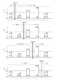
- FIG. 2 shows an example of the average voltage of the cells for each group when the cells Ce1 to Ce5 are divided into two groups.
- the five cells Ce1 to Ce5 connected in series are sequentially divided into two groups while maintaining the column order of the series connection. Then, the average voltage of the cells in each group is calculated.
- the average voltage of the entire cell is a reference voltage of 0V
- the cell Ce1 is ⁇ 1V
- the cell Ce2 is ⁇ 2V
- the cell Ce3 is + 1V
- the cell Ce4 is + 3V
- the cell Ce5 is ⁇ 1V.
- FIG. 2 (a) shows that when divided into the group of only the cell Ce1 and the group of the cells Ce2 to Ce5, the average voltage of the group of only the cell Ce1 is ⁇ 1V and the average voltage of the group of the cells Ce2 to Ce5 is +0 An example calculated as .25V is shown.
- the group boundary is between the cell Ce1 and the cell Ce2.
- the cell Ce1 and the cell Ce2 are cells located at the boundary of the group, and are also adjacent cells located at the boundary of the two groups.
- FIG. 2B shows an average voltage ⁇ 1.5 V of the group of cell Ce1 to cell Ce2 and cell Ce3 to cell Ce5 when divided into a group of cell Ce1 to cell Ce2 and a group of cell Ce3 to cell Ce5.
- FIG. 2 (c) shows that when the cell Ce1 to cell Ce3 and the cell Ce4 to cell Ce5 are divided into groups, the average voltage of the cell Ce1 to cell Ce3 is ⁇ 0.67 V, and the cell Ce4 to cell Ce5.
- the average voltage of the cell Ce1 to cell Ce3 is ⁇ 0.67 V
- FIG. 2D shows an average voltage + 0.25V of the group of the cells Ce1 to Ce4 and an average voltage of the group of only the cell Ce5 when divided into the group of the cells Ce1 to Ce4 and the group of only the cell Ce5.
- An example calculated as ⁇ 1V is shown.
- a switching converter SC12 is interposed between the cell Ce1 and the cell Ce2
- a switching converter SC23 is interposed between the cell Ce2 and the cell Ce3
- a switching converter SC34 is interposed between the cell Ce3 and the cell Ce4.
- a switching converter SC45 is interposed between the cell Ce4 and the cell Ce5.
- the average voltage ⁇ 1.5V of the cells Ce1 and Ce2 is compared with the average voltage + 1V of the cells Ce3 to Ce5.
- Cell Ce2 of the group with the lower average voltage adjacent cell located at the boundary of the group with the lower average voltage
- cell Ce3 of the group with the higher average voltage cell located at the boundary of the group with the higher average voltage
- the outflow / inflow of current by the switching converter SC23 stops when the average voltage of the cells Ce1, C2 and 2 becomes equal to or exceeds the average voltage of the cells Ce3 to Ce5.
- it may be configured to stop when any one of the average voltage of the cells Ce1 and Ce2 or the average voltage of the cells Ce3 to Ce5 is equal to or less than a predetermined threshold value.
- the charge moving direction is determined based on the average voltage of the cells in the groups on both sides.
- Each switching converter SC12, SC23, SC34, SC45 can be configured to drive each switch element simultaneously or in parallel.
- each switching converter is not affected by the operation of other switching converters. This is because, for example, when attention is paid to the switching converter SC23, the operation of the switching converter SC23 is charge transfer only between the cell Ce2 and the cell Ce3, and the average voltage of the group due to other grouping does not change by this charge transfer. Because.
- the charge transfer by the other switching converters SC12, SC34, SC45 does not affect the operation of the switching converter SC23. That is, the charge transfer by the switching converter SC12 is only charge transfer between the cell Ce1 and the cell Ce2, and the charge transfer by the switching converter SC34 is only charge transfer between the cell Ce3 and the cell Ce4. Since the charge transfer by the SC45 is a charge transfer only between the cell Ce4 and the cell Ce5, it does not affect the average voltage of the group of the cell Ce1 and the cell Ce2 and the group of the cell Ce3 to the cell Ce5.
- the switching converters SC12, SC23, SC34, and SC45 can be driven independently, and the control unit 1-4 drives the switching converters SC12, SC23, SC34, and SC45 simultaneously or in parallel, thereby It is possible to shorten the balance operation time.
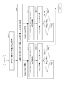
- FIG. 3 shows the flow of the first embodiment of the cell balance method according to the present invention.
- FIG. 3 shows an operation example of charge transfer with respect to adjacent cells in the m-th and m + 1-th column order of cells connected in series. It is assumed that the total number of cells is n.
- Av m is larger than Av m + 1 as a result of the comparison, ON / OFF control of the switch element is performed so as to move the charge from the m-th cell to the m + 1-th cell (S3-2). Then, Av m and Av m + 1 after the charge transfer are calculated, and the magnitudes are compared (S3-3). When Av m is still larger than Av m + 1 (S3-4 YES), ON / OFF control of the switch element is performed again so as to move the charge from the mth cell to the m + 1st cell (S3-2). If Av m is equal to Av m + 1 less than or Av m + 1 (S3-4NO), the operation ends.
- FIG. 4 shows a flow of a second embodiment of the cell balance method according to the present invention.
- FIG. 4 shows an example of the charge transfer operation for the m-th and m + 1-th adjacent columns of cells connected in series, and the total number of cells is n.
- the average voltage of only one cell in the group divided into two and the average voltage of the whole cell are calculated, and the charge movement direction is determined by comparing the magnitudes.
- the average voltage of one group is lower than the average voltage of the other group, the average voltage of the one group is lower than the average voltage of the whole cell. Is higher than the average voltage of the entire cell.
- the charge transfer direction can be determined by comparing the average voltage of one group with the average voltage of the entire cell.
- the second embodiment is based on such an operation principle.
- the average voltage Av n of all n cells is calculated (S4-1).
- the average voltage Av m of the first to m-th cell groups is calculated, and Av m and Av n are compared in magnitude (S4-2).
- Av m is larger than Av n as a result of the comparison, ON / OFF control of the switch element is performed so as to move the charge from the m-th cell to the m + 1-th cell (S4-3). Then, Av m after the charge transfer is calculated, and the magnitude is compared with Av n (S4-4). When Av m is still larger than Av n (S4-5 YES), the switch element is turned ON / OFF again to move the charge from the mth cell to the m + 1st cell (S4-3). If Av m is equal to Av n less than or Av n (S4-5NO), the operation ends.
- the cell balance by the charge transfer between the adjacent cells at the group boundary position by the two grouping described above may be performed simultaneously between the adjacent cells at the group boundary position of each grouping. You may go sequentially in sequence.
- the present invention is not limited to the above-described embodiment, and various configurations or embodiments can be taken without departing from the gist of the present invention.
Landscapes
- Engineering & Computer Science (AREA)
- Power Engineering (AREA)
- Charge And Discharge Circuits For Batteries Or The Like (AREA)
- Secondary Cells (AREA)
Priority Applications (3)
| Application Number | Priority Date | Filing Date | Title |
|---|---|---|---|
| EP13830364.9A EP2887495A4 (en) | 2012-08-20 | 2013-08-12 | CELL COMPENSATOR AND CELL COMPENSATION METHOD |
| CN201380040340.0A CN104508940A (zh) | 2012-08-20 | 2013-08-12 | 单元电池平衡设备和单元电池平衡方法 |
| US14/412,075 US20150171643A1 (en) | 2012-08-20 | 2013-08-12 | Cell balance apparatus and cell balance method |
Applications Claiming Priority (2)
| Application Number | Priority Date | Filing Date | Title |
|---|---|---|---|
| JP2012-181591 | 2012-08-20 | ||
| JP2012181591A JP5817678B2 (ja) | 2012-08-20 | 2012-08-20 | セルバランス装置及びセルバランス方法 |
Publications (1)
| Publication Number | Publication Date |
|---|---|
| WO2014030569A1 true WO2014030569A1 (ja) | 2014-02-27 |
Family
ID=50149878
Family Applications (1)
| Application Number | Title | Priority Date | Filing Date |
|---|---|---|---|
| PCT/JP2013/071806 Ceased WO2014030569A1 (ja) | 2012-08-20 | 2013-08-12 | セルバランス装置及びセルバランス方法 |
Country Status (5)
| Country | Link |
|---|---|
| US (1) | US20150171643A1 (enExample) |
| EP (1) | EP2887495A4 (enExample) |
| JP (1) | JP5817678B2 (enExample) |
| CN (1) | CN104508940A (enExample) |
| WO (1) | WO2014030569A1 (enExample) |
Families Citing this family (6)
| Publication number | Priority date | Publication date | Assignee | Title |
|---|---|---|---|---|
| JP6133110B2 (ja) * | 2013-04-09 | 2017-05-24 | Evtd株式会社 | バランス補正装置および蓄電システム |
| JP6234049B2 (ja) * | 2013-04-09 | 2017-11-22 | NExT−e Solutions株式会社 | バランス補正装置および蓄電システム |
| CN105210259B (zh) | 2013-04-09 | 2018-07-27 | 日商艾达司股份有限公司 | 平衡校正装置及蓄电系统 |
| EP3333008B1 (en) * | 2016-12-12 | 2022-06-15 | Honeywell International Inc. | Adaptive balancing for battery management |
| JP2025039244A (ja) * | 2023-09-08 | 2025-03-21 | 株式会社東芝 | 電池パックの管理装置、蓄電システム、電池パックの管理方法、及び、電池パックの管理プログラム |
| CN118399554B (zh) * | 2024-06-26 | 2024-10-29 | 比亚迪股份有限公司 | 均衡电路、均衡方法、电子设备、电池管理系统和车辆 |
Citations (4)
| Publication number | Priority date | Publication date | Assignee | Title |
|---|---|---|---|---|
| JP2003513605A (ja) * | 1999-11-05 | 2003-04-08 | パワー デザイナーズ リミテッド ライアビリティ カンパニー | モジュール式バッテリ充電等化器及び制御方法 |
| JP2008042970A (ja) * | 2006-08-01 | 2008-02-21 | Fdk Corp | 多直列蓄電セル |
| JP2010220373A (ja) | 2009-03-17 | 2010-09-30 | Fuji Electric Systems Co Ltd | 蓄電素子のバランス回路 |
| WO2013114696A1 (ja) * | 2012-01-31 | 2013-08-08 | 株式会社豊田自動織機 | 均等化装置 |
Family Cites Families (4)
| Publication number | Priority date | Publication date | Assignee | Title |
|---|---|---|---|---|
| US5479083A (en) * | 1993-06-21 | 1995-12-26 | Ast Research, Inc. | Non-dissipative battery charger equalizer |
| KR101220339B1 (ko) * | 2007-10-16 | 2013-01-09 | 한국과학기술원 | 직렬연결 배터리 스트링을 위한 자동 전하 균일 방법 및장치 |
| JP5197891B2 (ja) * | 2011-05-24 | 2013-05-15 | パナソニック株式会社 | 蓄電装置、携帯機器及び電動車両 |
| EP2541728A2 (en) * | 2011-06-30 | 2013-01-02 | Kabushiki Kaisha Toyota Jidoshokki | Cell balancing device |
-
2012
- 2012-08-20 JP JP2012181591A patent/JP5817678B2/ja not_active Expired - Fee Related
-
2013
- 2013-08-12 EP EP13830364.9A patent/EP2887495A4/en not_active Withdrawn
- 2013-08-12 US US14/412,075 patent/US20150171643A1/en not_active Abandoned
- 2013-08-12 CN CN201380040340.0A patent/CN104508940A/zh active Pending
- 2013-08-12 WO PCT/JP2013/071806 patent/WO2014030569A1/ja not_active Ceased
Patent Citations (4)
| Publication number | Priority date | Publication date | Assignee | Title |
|---|---|---|---|---|
| JP2003513605A (ja) * | 1999-11-05 | 2003-04-08 | パワー デザイナーズ リミテッド ライアビリティ カンパニー | モジュール式バッテリ充電等化器及び制御方法 |
| JP2008042970A (ja) * | 2006-08-01 | 2008-02-21 | Fdk Corp | 多直列蓄電セル |
| JP2010220373A (ja) | 2009-03-17 | 2010-09-30 | Fuji Electric Systems Co Ltd | 蓄電素子のバランス回路 |
| WO2013114696A1 (ja) * | 2012-01-31 | 2013-08-08 | 株式会社豊田自動織機 | 均等化装置 |
Non-Patent Citations (1)
| Title |
|---|
| See also references of EP2887495A4 |
Also Published As
| Publication number | Publication date |
|---|---|
| US20150171643A1 (en) | 2015-06-18 |
| EP2887495A1 (en) | 2015-06-24 |
| JP2014039435A (ja) | 2014-02-27 |
| JP5817678B2 (ja) | 2015-11-18 |
| EP2887495A4 (en) | 2016-01-13 |
| CN104508940A (zh) | 2015-04-08 |
Similar Documents
| Publication | Publication Date | Title |
|---|---|---|
| WO2014030569A1 (ja) | セルバランス装置及びセルバランス方法 | |
| CN106575928B (zh) | 模块化能量存储器直接转换器系统 | |
| JP6465358B2 (ja) | 電圧均等化回路システム | |
| CN102170029B (zh) | 能量转移型的动力电池组快速均衡系统及控制方法 | |
| US9270132B2 (en) | Balancing method and battery system | |
| US9356467B2 (en) | Charge balancing circuit for series connected chains of charge storage elements | |
| CN105656142B (zh) | 一种锂离子动力电池组充放电主动均衡电路 | |
| JP6065782B2 (ja) | 蓄電装置、充電方法及び放電方法 | |
| CN102882242B (zh) | 蓄电池组充电及放电平衡的电路 | |
| KR20140106982A (ko) | 배터리에 포함된 셀들의 밸런싱을 수행하는 밸런싱 장치 및 배터리 모듈 | |
| US20180309384A1 (en) | Single-Phase Four-Level Inverter Circuit Topology and Three-Phase Four-Level Inverter Circuit Topology | |
| CN108599282A (zh) | 一种锂离子动力电池组充放电主动均衡系统及方法 | |
| JP6135375B2 (ja) | 蓄電装置、充電方法及び放電方法 | |
| CN103607115B (zh) | 电荷泵装置 | |
| CN103684018A (zh) | 新颖的多电平逆变器电容电压平衡电路及控制方法 | |
| JP2014039435A5 (enExample) | ||
| JP2013192371A (ja) | 蓄電装置、充電方法及び放電方法 | |
| WO2021010388A1 (ja) | 電池管理回路および蓄電装置 | |
| CN203747684U (zh) | 多电平逆变器电容电压平衡电路 | |
| CN105490329A (zh) | 基于电感充放电能量转移的串联电池组均衡电路 | |
| CN120481753A (zh) | 一种充电方法、充电桩及充电系统 | |
| CN204258365U (zh) | 电池组主动均衡级联结构 | |
| JP2016046836A (ja) | 非絶縁型セルバランス回路 | |
| CN204258367U (zh) | 基于外部控制反激电路的电池组双向主动均衡电路 | |
| CN203590027U (zh) | 功率电荷泵 |
Legal Events
| Date | Code | Title | Description |
|---|---|---|---|
| 121 | Ep: the epo has been informed by wipo that ep was designated in this application |
Ref document number: 13830364 Country of ref document: EP Kind code of ref document: A1 |
|
| WWE | Wipo information: entry into national phase |
Ref document number: 14412075 Country of ref document: US |
|
| REEP | Request for entry into the european phase |
Ref document number: 2013830364 Country of ref document: EP |
|
| WWE | Wipo information: entry into national phase |
Ref document number: 2013830364 Country of ref document: EP |
|
| NENP | Non-entry into the national phase |
Ref country code: DE |