WO2014027588A1 - 固体撮像装置および電子機器 - Google Patents
固体撮像装置および電子機器 Download PDFInfo
- Publication number
- WO2014027588A1 WO2014027588A1 PCT/JP2013/071338 JP2013071338W WO2014027588A1 WO 2014027588 A1 WO2014027588 A1 WO 2014027588A1 JP 2013071338 W JP2013071338 W JP 2013071338W WO 2014027588 A1 WO2014027588 A1 WO 2014027588A1
- Authority
- WO
- WIPO (PCT)
- Prior art keywords
- photoelectric conversion
- imaging device
- pixel
- solid
- state imaging
- Prior art date
- Legal status (The legal status is an assumption and is not a legal conclusion. Google has not performed a legal analysis and makes no representation as to the accuracy of the status listed.)
- Ceased
Links
Images














Classifications
-
- H—ELECTRICITY
- H10—SEMICONDUCTOR DEVICES; ELECTRIC SOLID-STATE DEVICES NOT OTHERWISE PROVIDED FOR
- H10K—ORGANIC ELECTRIC SOLID-STATE DEVICES
- H10K39/00—Integrated devices, or assemblies of multiple devices, comprising at least one organic radiation-sensitive element covered by group H10K30/00
- H10K39/30—Devices controlled by radiation
- H10K39/32—Organic image sensors
-
- H—ELECTRICITY
- H04—ELECTRIC COMMUNICATION TECHNIQUE
- H04N—PICTORIAL COMMUNICATION, e.g. TELEVISION
- H04N23/00—Cameras or camera modules comprising electronic image sensors; Control thereof
- H04N23/10—Cameras or camera modules comprising electronic image sensors; Control thereof for generating image signals from different wavelengths
- H04N23/12—Cameras or camera modules comprising electronic image sensors; Control thereof for generating image signals from different wavelengths with one sensor only
-
- H—ELECTRICITY
- H04—ELECTRIC COMMUNICATION TECHNIQUE
- H04N—PICTORIAL COMMUNICATION, e.g. TELEVISION
- H04N25/00—Circuitry of solid-state image sensors [SSIS]; Control thereof
- H04N25/70—SSIS architectures; Circuits associated therewith
-
- H—ELECTRICITY
- H04—ELECTRIC COMMUNICATION TECHNIQUE
- H04N—PICTORIAL COMMUNICATION, e.g. TELEVISION
- H04N25/00—Circuitry of solid-state image sensors [SSIS]; Control thereof
- H04N25/70—SSIS architectures; Circuits associated therewith
- H04N25/76—Addressed sensors, e.g. MOS or CMOS sensors
- H04N25/78—Readout circuits for addressed sensors, e.g. output amplifiers or A/D converters
-
- H—ELECTRICITY
- H10—SEMICONDUCTOR DEVICES; ELECTRIC SOLID-STATE DEVICES NOT OTHERWISE PROVIDED FOR
- H10F—INORGANIC SEMICONDUCTOR DEVICES SENSITIVE TO INFRARED RADIATION, LIGHT, ELECTROMAGNETIC RADIATION OF SHORTER WAVELENGTH OR CORPUSCULAR RADIATION
- H10F39/00—Integrated devices, or assemblies of multiple devices, comprising at least one element covered by group H10F30/00, e.g. radiation detectors comprising photodiode arrays
- H10F39/10—Integrated devices
- H10F39/12—Image sensors
- H10F39/18—Complementary metal-oxide-semiconductor [CMOS] image sensors; Photodiode array image sensors
- H10F39/182—Colour image sensors
-
- H—ELECTRICITY
- H10—SEMICONDUCTOR DEVICES; ELECTRIC SOLID-STATE DEVICES NOT OTHERWISE PROVIDED FOR
- H10F—INORGANIC SEMICONDUCTOR DEVICES SENSITIVE TO INFRARED RADIATION, LIGHT, ELECTROMAGNETIC RADIATION OF SHORTER WAVELENGTH OR CORPUSCULAR RADIATION
- H10F39/00—Integrated devices, or assemblies of multiple devices, comprising at least one element covered by group H10F30/00, e.g. radiation detectors comprising photodiode arrays
- H10F39/10—Integrated devices
- H10F39/12—Image sensors
- H10F39/199—Back-illuminated image sensors
-
- H—ELECTRICITY
- H10—SEMICONDUCTOR DEVICES; ELECTRIC SOLID-STATE DEVICES NOT OTHERWISE PROVIDED FOR
- H10K—ORGANIC ELECTRIC SOLID-STATE DEVICES
- H10K19/00—Integrated devices, or assemblies of multiple devices, comprising at least one organic element specially adapted for rectifying, amplifying, oscillating or switching, covered by group H10K10/00
- H10K19/20—Integrated devices, or assemblies of multiple devices, comprising at least one organic element specially adapted for rectifying, amplifying, oscillating or switching, covered by group H10K10/00 comprising components having an active region that includes an inorganic semiconductor
-
- H—ELECTRICITY
- H10—SEMICONDUCTOR DEVICES; ELECTRIC SOLID-STATE DEVICES NOT OTHERWISE PROVIDED FOR
- H10K—ORGANIC ELECTRIC SOLID-STATE DEVICES
- H10K30/00—Organic devices sensitive to infrared radiation, light, electromagnetic radiation of shorter wavelength or corpuscular radiation
- H10K30/80—Constructional details
- H10K30/81—Electrodes
-
- Y—GENERAL TAGGING OF NEW TECHNOLOGICAL DEVELOPMENTS; GENERAL TAGGING OF CROSS-SECTIONAL TECHNOLOGIES SPANNING OVER SEVERAL SECTIONS OF THE IPC; TECHNICAL SUBJECTS COVERED BY FORMER USPC CROSS-REFERENCE ART COLLECTIONS [XRACs] AND DIGESTS
- Y02—TECHNOLOGIES OR APPLICATIONS FOR MITIGATION OR ADAPTATION AGAINST CLIMATE CHANGE
- Y02E—REDUCTION OF GREENHOUSE GAS [GHG] EMISSIONS, RELATED TO ENERGY GENERATION, TRANSMISSION OR DISTRIBUTION
- Y02E10/00—Energy generation through renewable energy sources
- Y02E10/50—Photovoltaic [PV] energy
- Y02E10/549—Organic PV cells
Definitions
- the present disclosure relates to a solid-state imaging device and an electronic device including a photoelectric conversion element as a pixel.
- a solid-state imaging device such as a CCD (Charge-Coupled Device) image sensor or a CMOS (Complementary Metal-Oxide Semiconductor) image sensor
- photoelectric conversion layers of a plurality of colors for example, R, G, B
- a device that obtains signals of three colors from a pixel has been proposed (for example, Patent Document 1).
- an organic photoelectric conversion unit that detects green light and generates a signal charge according to the green light is provided on a silicon substrate, and red light and blue light are detected in the silicon substrate, respectively.
- a photodiode inorganic photoelectric conversion unit
- a solid-state imaging device includes a plurality of pixels each including at least two first and second photoelectric conversion units stacked, and the first and second photoelectric devices are provided for each pixel.
- the rates of change of the sensitivity of the conversion units with respect to the light incident angle are equal to each other.
- An electronic apparatus includes the solid-state imaging device according to the embodiment of the present disclosure.
- the rate of change of the sensitivity of each of the stacked first and second photoelectric conversion units with respect to the light incident angle (the light incident angle is changed) for each pixel. are equal to each other), the ratio of the pixel output obtained from each photoelectric conversion unit becomes constant regardless of the light incident angle.
- the rate of change of the sensitivity of each of the stacked first and second photoelectric conversion units with respect to the light incident angle is equal to each other for each pixel. Therefore, fluctuations in the ratio of pixel outputs obtained from the respective photoelectric conversion units can be reduced. Therefore, color reproducibility can be improved regardless of signal processing.
- FIG. 10 is a cross-sectional diagram illustrating a process following the process in FIG. 9.
- FIG. 11 is a cross-sectional diagram illustrating a process following the process in FIG. 10. It is sectional drawing showing the process of following FIG. 11A.
- FIG. 10 is a cross-sectional diagram illustrating a process following the process in FIG. 9.
- FIG. 11B is a cross-sectional diagram illustrating a process following the process in FIG. 11B.
- FIG. 13 is a cross-sectional diagram illustrating a process following the process in FIG. 12.
- FIG. 14 is a cross-sectional diagram illustrating a process following the process in FIG. 13. It is a characteristic view for demonstrating the light incident angle dependence of a sensitivity. It is a characteristic view for demonstrating the light incident angle dependence of a sensitivity. It is a schematic diagram for demonstrating the relationship between an opening area and a sensitivity. It is a schematic diagram for demonstrating the relationship between an opening area and a sensitivity. It is a schematic diagram for demonstrating the relationship between an opening area and a sensitivity. It is a schematic diagram for demonstrating the relationship between an opening area and a sensitivity.
- FIG. 21A and FIG. 21B It is a schematic diagram showing the example of a layout of the pixel shown to FIG. 21A and FIG. 21B. It is sectional drawing showing the principal part structure of the photoelectric conversion element (pixel) of 6th Embodiment of this indication. It is sectional drawing showing the principal part structure of the photoelectric conversion element (pixel) of 6th Embodiment of this indication. It is a characteristic view for demonstrating the light incident angle dependence of the sensitivity of the pixel shown to FIG. 23A. It is a characteristic view for demonstrating the light incident angle dependence of the sensitivity of the pixel shown to FIG. 23A. It is a characteristic view for demonstrating the light incident angle dependence of the sensitivity of the pixel shown to FIG. 23B. It is a characteristic view for demonstrating the light incident angle dependence of the sensitivity of the pixel shown to FIG. It is a functional block diagram of a solid-state imaging device. It is a functional block diagram of the electronic device which concerns on an application example.
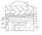
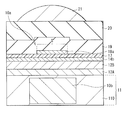
- FIG. 1 illustrates a schematic cross-sectional configuration of a pixel (photoelectric conversion element 10) in the solid-state imaging device according to the first embodiment of the present disclosure.
- the solid-state imaging device is, for example, a CCD (Charge Coupled Device) or a CMOS (Complementary Metal Oxide Semiconductor) image sensor.
- CMOS Complementary Metal Oxide Semiconductor
- pixel transistors including transfer transistors Tr1 to 3 described later
- a layer multilayer wiring layer 51
- the photoelectric conversion element 10 includes, for example, an organic photoelectric conversion unit 10a (first photoelectric conversion unit) and an inorganic photoelectric conversion unit 10b (second photoelectric conversion unit) that perform photoelectric conversion by selectively detecting light having different wavelengths. ) In the vertical direction.
- the organic photoelectric conversion unit 10a is formed on the semiconductor substrate 11 and includes an organic photoelectric conversion layer (organic photoelectric conversion layer 17).
- the inorganic photoelectric conversion unit 10 b is formed in the semiconductor substrate 11. Thereby, in the solid-state imaging device described later, a plurality of types of color signals can be acquired in one pixel without using a color filter.
- the photoelectric conversion element 10 has a laminated structure of one organic photoelectric conversion unit 11G and two inorganic photoelectric conversion layers 11B and 11R. Each color signal of red (R), green (G), and blue (B) is acquired.
- the organic photoelectric conversion unit 11G includes, for example, an organic photoelectric conversion layer 17G that detects green light (performs green light photoelectric conversion), and the inorganic photoelectric conversion unit 10b includes, for example, an inorganic photoelectric conversion layer 11B that detects blue light. And an inorganic photoelectric conversion layer 11R that detects red light.
- the semiconductor substrate 11 is, for example, one in which inorganic photoelectric conversion layers 11B and 11R and a green power storage layer 110G are embedded in a predetermined region of an n-type silicon (Si) layer 110. Also embedded in the semiconductor substrate 11 is a conductive plug 120a1 serving as a transmission path for charges (electrons or holes) from the organic photoelectric conversion unit 11G.
- the back surface (surface S1) of the semiconductor substrate 11 is a light receiving surface.
- a peripheral circuit composed of a logic circuit or the like is formed.
- Examples of the pixel transistor include a transfer transistor, a reset transistor, an amplification transistor, and a selection transistor.
- Each of these pixel transistors is formed of a MOS transistor, for example, and is formed in the p-type semiconductor well region on the surface S2.
- a circuit including such a pixel transistor is formed for each of the red, green, and blue photoelectric conversion units.
- Each circuit may have a three-transistor configuration including a total of three transistors, such as a transfer transistor, a reset transistor, and an amplifying transistor, among these pixel transistors, or four transistors including a selection transistor. It may be a configuration.
- the transfer transistors Tr1 to Tr3 are illustrated.
- the pixel transistors other than the transfer transistor can be shared between the photoelectric conversion units or between the pixels. Further, a so-called pixel sharing structure that shares a floating diffusion can also be applied.
- the transfer transistors Tr1 to Tr3 are configured to include gate electrodes (gate electrodes TG1 to TG3) and floating diffusions (FDs 113, 114, and 116).
- the transfer transistor Tr1 transfers the signal charge corresponding to green (electrons in the present embodiment) generated in the organic photoelectric conversion unit 11G and accumulated in the green power storage layer 110G to a vertical signal line Lsig described later. It is.
- the transfer transistor Tr2 transfers signal charges (electrons in the present embodiment) corresponding to blue generated and accumulated in the inorganic photoelectric conversion layer 11B to a vertical signal line Lsig described later.
- the transfer transistor Tr3 transfers signal charges (electrons in the present embodiment) corresponding to red color generated and accumulated in the inorganic photoelectric conversion layer 11R to a vertical signal line Lsig described later.
- Each of the inorganic photoelectric conversion layers 11B and 11R is a photodiode having a pn junction (Photo Diode), and is formed in the semiconductor substrate 11 in the order of, for example, the surface S1 side (light incident side) to the inorganic photoelectric conversion layers 11B and 11R.
- the inorganic photoelectric conversion layer 11 ⁇ / b> B selectively detects blue light and accumulates signal charges corresponding to blue.
- the inorganic photoelectric conversion layer 11 ⁇ / b> B has a multilayer structure from a selective region along the surface S ⁇ b> 1 of the semiconductor substrate 11. It is formed to extend over a region near the interface with the wiring layer 51.
- the inorganic photoelectric conversion layer 11R selectively detects red light and accumulates signal charges corresponding to red, and is formed, for example, in a region below the inorganic photoelectric conversion layer 11B (surface S2 side). .
- blue (B) is a color corresponding to, for example, a wavelength range of 450 nm to 495 nm
- red (R) is a color corresponding to a wavelength range of, for example, 620 nm to 750 nm
- the inorganic photoelectric conversion layers 11B and 11R are respectively the above wavelength ranges. It is sufficient that light in a part or all of the wavelength region can be detected.
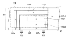
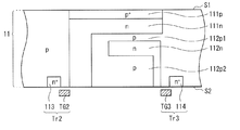
- FIG. 3A and 3B show detailed configuration examples of the inorganic photoelectric conversion layers 11B and 11R.
- FIG. 3A and FIG. 3B show configurations in different cross sections. Note that in this embodiment, a case where electrons out of a pair of electrons and holes generated by photoelectric conversion are read as signal charges (when an n-type semiconductor region is a photoelectric conversion layer) will be described. In the figure, “+ (plus)” superscripted on “p” and “n” represents a high p-type or n-type impurity concentration.
- the gate electrodes TG2 and TG3 of the transfer transistors Tr2 and Tr3 are also shown.
- the inorganic photoelectric conversion layer 11B includes, for example, a p-type semiconductor region serving as a hole storage layer (hereinafter also referred to simply as a p-type region, the same applies to an n-type case) 111p, and an n-type photoelectric conversion layer serving as an electron storage layer ( n-type region) 111n.
- a p-type semiconductor region serving as a hole storage layer (hereinafter also referred to simply as a p-type region, the same applies to an n-type case) 111p
- an n-type photoelectric conversion layer serving as an electron storage layer ( n-type region) 111n.
- Each of the p-type region 111p and the n-type photoelectric conversion layer 111n is formed in a selective region in the vicinity of the surface S1, and a part thereof is bent so as to extend to reach the interface with the surface S2. .
- the p-type region 111p is connected to a p-type semiconductor well region (
- the n-type photoelectric conversion layer 111n is connected to the FD 113 (n-type region) of the blue transfer transistor Tr2. Note that a p-type region 113p (a hole accumulation layer) is formed in the vicinity of the interface between each surface S2 side end of the p-type region 111p and the n-type photoelectric conversion layer 111n and the surface S2.
- the inorganic photoelectric conversion layer 11R is formed, for example, by sandwiching an n-type photoelectric conversion layer 112n (electron storage layer) between p-type regions 112p1 and 112p2 (hole storage layer) (p-np stacked structure). Have). A part of the n-type photoelectric conversion layer 112n is bent and extended so as to reach the interface with the surface S2. The n-type photoelectric conversion layer 112n is connected to the FD 114 (n-type region) of the red transfer transistor Tr3. Note that a p-type region 113p (hole accumulation layer) is formed at least near the interface between the end of the n-type photoelectric conversion layer 111n on the surface S2 side and the surface S2.
- FIG. 4 shows a detailed configuration example of the green electricity storage layer 110G.
- a description will be given of a case where electrons are read out from the lower electrode 14a side as signal charges out of a pair of electrons and holes generated by the organic photoelectric conversion unit 11G.
- FIG. 4 also shows the gate electrode TG1 of the transfer transistor Tr1 among the pixel transistors.
- the green power storage layer 110G includes an n-type region 115n that serves as an electron storage layer.
- a part of the n-type region 115n is connected to the conductive plug 120a1, and accumulates electrons supplied from the lower electrode 14a side through the conductive plug 120a1.
- the n-type region 115n is also connected to the FD 116 (n-type region) of the green transfer transistor Tr1.
- a p-type region 115p (hole accumulation layer) is formed in the vicinity of the interface between the n-type region 115n and the surface S2.
- the conductive plug 120a1 together with a conductive plug 120a2 described later, functions as a connector between the organic photoelectric conversion unit 11G and the semiconductor substrate 11, and forms a transmission path for electrons or holes generated in the organic photoelectric conversion unit 11G. is there.
- the conductive plug 120a1 is electrically connected to the lower electrode 14a of the organic photoelectric conversion unit 11G and is connected to the green power storage layer 110G.
- the conductive plug 120a1 is formed of, for example, a conductive semiconductor layer and is embedded in the semiconductor substrate 11. In this case, since it becomes an electron transmission path, the conductive plug 120a1 is preferably an n-type. Alternatively, the conductive plug 120a1 may be, for example, a through via filled with a conductive film material such as tungsten. In this case, for example, in order to suppress a short circuit with silicon, it is desirable that the via side surface be covered with an insulating film such as silicon oxide (SiO 2 ) or silicon nitride (SiN).
- SiO 2 silicon oxide
- SiN silicon nitride
- a support substrate 53 made of, for example, silicon is bonded to the surface S2 side of the semiconductor substrate 11 as described above with a multilayer wiring layer 51 interposed therebetween.
- a multilayer wiring layer 51 a plurality of wirings 51 a and wirings 51 b are arranged via an interlayer insulating film 52.
- the multilayer wiring layer 51 is formed on the side opposite to the light receiving surface, and a so-called back-illuminated solid-state imaging device can be realized.
- the organic photoelectric conversion unit 10a uses an organic semiconductor to absorb light having a selective wavelength (here, green light) and generate an electron / hole pair. It is a conversion element.
- the organic photoelectric conversion unit 10a (11G) has a configuration in which an organic photoelectric conversion layer 17 (17G) is sandwiched between a pair of electrodes (lower electrode 14a and upper electrode 18) for taking out signal charges.
- the lower electrode 14a (first electrode) is electrically connected to a conductive plug 120a1 embedded in the semiconductor substrate 11.
- the upper electrode 18 (second electrode) is connected to the wiring 51a in the multilayer wiring layer 51 via a contact portion (not shown), for example, at the periphery of the solid-state imaging device, and thereby charges (here, holes) are discharged. It has come to be.
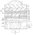
- FIG. 5 is a diagram for explaining a detailed configuration of the organic photoelectric conversion unit 11G.
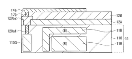
- the organic photoelectric conversion unit 11G is formed on the surface S1 of the semiconductor substrate 11 via interlayer insulating films 12A and 12B.
- a conductive plug 120a2 is embedded in a region facing the conductive plug 120a1
- a wiring layer 13a is embedded in a region facing the conductive plug 120a2.
- a lower electrode 14a is disposed on the interlayer insulating film 12B.
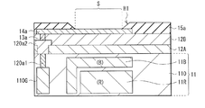
- An inter-pixel insulating film 15a is provided on the lower electrode 14a, and an opening H1 is provided in the inter-pixel insulating film 15a so as to face the lower electrode 14a.
- An organic photoelectric conversion layer 17G is formed from the inside of the opening H1 of the inter-pixel insulating film 15a (the upper surface of the lower electrode 14a) to the peripheral region thereof.
- An upper electrode 18 is provided so as to cover the organic photoelectric conversion layer 17G, and a protective film 19 and a planarizing layer 20 are laminated on the upper electrode 18 in this order.
- the conductive plug 120a2 functions as a connector together with the conductive plug 120a1, and together with the conductive plug 120a1 and the wiring layer 13a, a conductive (electron) transmission path from the lower electrode 14a to the green power storage layer 110G.
- the conductive plug 120a2 may function as a light shielding film.
- it is desirable that the conductive plug 120a2 is formed of a laminated film of a metal material such as titanium (Ti), titanium nitride (TiN), and tungsten.
- the interlayer insulating film 12A is made of an insulating film having a small interface state in order to reduce the interface state with the semiconductor substrate 11 (silicon layer 110) and to suppress the generation of dark current from the interface with the silicon layer 110. Desirably configured.
- an insulating film for example, a stacked film of a hafnium oxide (HfO 2 ) film and a silicon oxide (SiO 2 ) film can be used.
- the interlayer insulating film 12B is composed of, for example, a single layer film made of one of silicon oxide, silicon nitride, silicon oxynitride (SiON), or a laminated film made of two or more of these.
- the lower electrode 14a is provided in a region that faces the light receiving surfaces of the inorganic photoelectric conversion layers 11B and 11R formed in the semiconductor substrate 11 and covers these light receiving surfaces.
- the lower electrode 14a is light transmissive and is made of, for example, a conductive film having a refractive index of 1.8 to 2.0, such as ITO (indium tin oxide).
- ITO indium tin oxide
- tin oxide (TO), tin oxide (SnO 2 ) -based material added with a dopant, or zinc oxide-based material obtained by adding a dopant to zinc oxide (ZnO) may be used.
- the zinc oxide-based material examples include aluminum zinc oxide (AZO) to which aluminum (Al) is added as a dopant, gallium zinc oxide (GZO) to which gallium (Ga) is added, and indium zinc oxide to which indium (In) is added. (IZO).
- AZO aluminum zinc oxide
- GZO gallium zinc oxide
- Indium zinc oxide to which indium (In) is added.
- IZO indium zinc oxide to which indium (In) is added.
- CuI, InSbO 4 , ZnMgO, CuInO 2 , MgIN 2 O 4 , CdO, ZnSnO 3, or the like may be used.
- signal charges are extracted from the lower electrode 14a as described above, in the solid-state imaging device described later using the photoelectric conversion element 10 as a pixel, the lower electrode 14a is a pixel. Each pixel is separated by the inter-layer insulating film 15a.
- the inter-pixel insulating film 15a is composed of, for example, a single layer film made of one of silicon oxide, silicon nitride, silicon oxynitride (SiON), or the like, or a laminated film made of two or more of these. .
- These inter-pixel insulating films 15a have a function of electrically separating the lower electrodes 14a of the respective pixels when the photoelectric conversion element 10 is used as a pixel of the solid-state imaging device.
- the opening shape and size of the opening H1 of the inter-pixel insulating film 15a are set so that the sensitivity (sensitivity to the light incident angle) in the organic photoelectric conversion unit 11G exhibits predetermined characteristics. Yes.
- the organic photoelectric conversion layer 17 is composed of an organic semiconductor that absorbs light in a selective wavelength range and performs photoelectric conversion while transmitting light in other wavelength ranges.
- the organic semiconductor is preferably configured to include one or both of an organic p-type semiconductor and an organic n-type semiconductor.
- an organic semiconductor any one of quinacridone derivatives, naphthalene derivatives, anthracene derivatives, phenanthrene derivatives, tetracene derivatives, pyrene derivatives, perylene derivatives, and fluoranthene derivatives is preferably used.
- a polymer such as phenylene vinylene, fluorene, carbazole, indole, pyrene, pyrrole, picoline, thiophene, acetylene, diacetylene, or a derivative thereof may be used.
- metal complex dyes rhodamine dyes, cyanine dyes, merocyanine dyes, phenylxanthene dyes, triphenylmethane dyes, rhodacyanine dyes, xanthene dyes, macrocyclic azaannulene dyes, azulene dyes, naphthoquinones , Anthraquinone dyes, chain compounds condensed with condensed polycyclic aromatics and aromatic rings or heterocyclic compounds such as anthracene and pyrene, or quinoline, benzothiazole, benzoxazole having a squarylium group and a croconic methine group as a binding chain Or the like, or a cyanine-like dye bonded by two nitrogen-containing heterocycles or the like, or a squarylium group and a croconite methine group can be preferably used.
- the metal complex dye is preferably a dithiol metal complex dye, a metal phthalocyanine dye, a metal porphyrin dye, or a ruthenium complex dye, but is not limited thereto.
- the organic photoelectric conversion layer 17G can photoelectrically convert green light corresponding to a part or all of the wavelength range of 495 nm to 570 nm, for example, and one or more of the above materials It is comprised including the material of.
- the thickness of such an organic photoelectric conversion layer 17G is, for example, 50 nm to 500 nm.
- an organic co-deposition film that is a composite film of these organic semiconductors may be used as the organic photoelectric conversion layer 17.
- other layers may be provided between the lower electrode 14 a of the organic photoelectric conversion layer 17 and the upper electrode 18.
- an undercoat film, an electron blocking film, an organic photoelectric conversion layer 17, a hole blocking film, a buffer film, a work function adjusting film, and the like may be stacked sequentially from the lower electrode 14a side.
- the upper electrode 18 is composed of an inorganic conductive film having light transmittance similar to that of the lower electrode 14a. In the case where signal charges are extracted from the lower electrode 14a side as in the present embodiment, the upper electrode 18 is provided in common for each pixel.
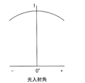
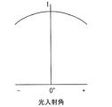
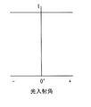
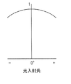
- the sensitivity of the organic photoelectric conversion unit 10a (11G) with respect to the light incident angle is equal to the light incident angle-sensitivity characteristic of the inorganic photoelectric conversion unit 10b (11B, 11R).
- FIG. 6A shows the light incident angle-sensitivity characteristic of the organic photoelectric conversion unit 10a (11G)
- FIG. 6B shows the light incident angle-sensitivity characteristic of the inorganic photoelectric conversion unit 10b (11B, 11R).
- the incident angle of the light beam incident along the direction perpendicular to the main surface of the semiconductor substrate 11 is a light incident angle of 0 °
- the sensitivity when the light incident angle is 0 ° is normalized as 1. Yes.
- the inorganic photoelectric conversion unit 10b has a structure in which two inorganic photoelectric conversion layers 11B and 11R are stacked, but the distance between these inorganic photoelectric conversion layers 11B and 11R (several tens nm to several hundreds nm). ) Is smaller than the distance (about several ⁇ m or less) between the organic photoelectric conversion portion.
- the light incident angle-sensitivity characteristics of the inorganic photoelectric conversion layers 11B and 11R formed in the semiconductor substrate 11 can be regarded as equivalent to each other.
- the light incident angle-sensitivity characteristic of the organic photoelectric conversion unit 10a (11G) is equivalent to the light incident angle-sensitivity characteristic of such an inorganic photoelectric conversion unit 10b (11B, 11R) (preferably The organic photoelectric conversion unit 10a (11G) is designed so as to completely match.
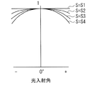
- the junction area S is determined for each pixel. Has been adjusted. As shown in FIG. 7, when the junction area S is gradually reduced (S1> S2> S3> S4), the sensitivity decreases in a range where the light incident angle is larger. In this embodiment, since the junction area S is equal to the opening area of the opening H1, the opening area is adjusted so that the above-described light incident angle-sensitivity characteristics can be obtained.
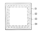
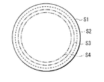
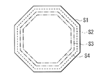
- FIG. 8A to 8C show examples of the shape of the opening H1 and the opening area.
- the opening shape of the opening H1 include a square (FIG. 8A), a circle (FIG. 8B), a regular octagon (FIG. 8C), and the like.
- the aperture area (S1, S2, S3, S4,...) Is set for each pixel so as to exhibit the above-described light incident angle-sensitivity characteristics. The smaller the aperture area, the higher the dependency of the sensitivity on the light incident angle (the sensitivity tends to decrease as the light incident angle increases).
- the protective film 19 is made of, for example, a light-transmitting inorganic material, and is made of, for example, a single-layer film made of any of silicon oxide, silicon nitride, silicon oxynitride, or the like, or two or more of them. It is a laminated film.
- the thickness of the protective film 19 is, for example, 0.1 ⁇ m to 30 ⁇ m.
- the planarizing layer 20 is made of, for example, an acrylic resin material, a styrene resin material, an epoxy resin material, or the like.
- An on-chip lens 21 is provided on the planarizing layer 20.
- the planarization layer 20 may be provided as necessary, and the protective layer 19 may also serve as the planarization layer 20.
- the on-chip lens 21 condenses light incident from above on the light receiving surfaces of the organic photoelectric conversion layer 17G and the inorganic photoelectric conversion layers 11B and 11R.
- the multilayer wiring layer 51 is formed on the surface S2 side of the semiconductor substrate 11, the light receiving surfaces of the organic photoelectric conversion layer 17G and the inorganic photoelectric conversion layers 11B and 11R are arranged close to each other. Thus, it is possible to reduce the variation in sensitivity between the colors depending on the F value of the on-chip lens 21.
- the photoelectric conversion element 10 as described above can be manufactured, for example, as follows. 9 to 14 show the method of manufacturing the photoelectric conversion element 10 in the order of steps. However, here, only the main configuration of the photoelectric conversion element 10 is illustrated, and a procedure for forming the organic photoelectric conversion unit 11G on the surface S1 side of the semiconductor substrate 11 will be specifically described.
- the semiconductor substrate 11 having the inorganic photoelectric conversion portions 10b (11B, 11R) is formed before the organic photoelectric conversion portion 11G is formed, and a multilayer wiring layer is formed on the surface S2 side of the semiconductor substrate 11. 51 and a support substrate 53 are formed. Specifically, first, a silicon layer 110 is formed on a temporary substrate made of, for example, a silicon oxide film, and the conductive plug 120a1, the green storage layer 110G, and the inorganic photoelectric conversion layers 11B and 11R are formed on the silicon layer 110. For example, the semiconductor substrate 11 is formed by embedding by ion implantation.
- a pixel transistor including transfer transistors Tr1 to Tr3, a peripheral circuit such as a logic circuit, and a multilayer wiring layer 51 are formed on the surface S2 side of the semiconductor substrate 11. Subsequently, after the support substrate 53 is bonded onto the multilayer wiring layer 51, the temporary substrate is peeled off from the surface S1 side of the semiconductor substrate 11 to expose the surface S1 of the semiconductor substrate 11.
- interlayer insulating films 12 ⁇ / b> A and 12 ⁇ / b> B are formed on the surface S ⁇ b> 1 of the semiconductor substrate 11.
- an interlayer insulating film 12A made of a laminated film of a hafnium oxide film and a silicon oxide film as described above is formed on the surface S1 of the semiconductor substrate 11.
- a hafnium oxide film is formed by an ALD (atomic layer deposition) method
- a silicon oxide film is formed by a plasma CVD method, for example.
- a region facing the conductive plug 120a1 of the interlayer insulating film 12A is opened, and the conductive plug 120a2 made of the above-described material is formed.
- an interlayer insulating film 12B made of the above-described material is formed on the interlayer insulating film 12A by, for example, a plasma CVD method. Next, a region of the interlayer insulating film 12B facing the conductive plug 120a2 is opened, and the wiring layer 13a made of the above-described material is formed.
- a lower electrode 14a is formed on the interlayer insulating film 12B.
- the above-described transparent conductive film is formed over the entire surface of the interlayer insulating film 12B.
- film forming methods include sol-gel method, spin coating method, spray method, roll coating method, ion beam deposition (Ion Beam deposition) method, electron beam deposition (electron beam deposition) method, laser ablation (laser ablation) method, CVD Method or sputtering method.
- Ion Beam deposition ion Beam deposition
- electron beam deposition electron beam deposition
- laser ablation laser ablation
- CVD Method or sputtering method.
- the lower electrode 14a is formed by patterning, for example, using dry etching (or wet etching) using a photolithography method. At this time, by forming the lower electrode 14a in a region facing the wiring layer 13a, the lower electrode 14a is electrically connected to the green power storage layer 110G via the wiring layer 13a and the conductive plugs 120a1 and 120a2. Like that.
- an inter-pixel insulating film 15a is formed.
- the inter-pixel insulating film 15a made of the above-described material is formed by, for example, the plasma CVD method so as to cover the interlayer insulating film 12B and the lower electrode 14a over the entire surface of the semiconductor substrate 11.
- the surface of the formed inter-pixel insulating film 15a is planarized by using, for example, a CMP (Chemical Mechanical Polishing) method.
- an opening H1 is formed in the inter-pixel insulating film 15a.
- the region facing the lower electrode 14a of the inter-pixel insulating film 15a is selectively removed by, for example, dry etching using a photolithography method. Thereby, the surface of the lower electrode 14a is exposed from the inter-pixel insulating film 15a.
- the opening area (contact area S), the shape, and the like of the opening H1 are set so as to exhibit the above-described light incident angle-sensitivity characteristics.
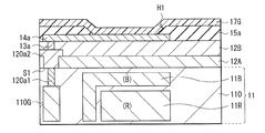
- an organic photoelectric conversion layer 17G made of the above-described material or the like is formed using, for example, a vacuum evaporation method. Thereby, the organic photoelectric conversion layer 17G is formed in contact with the lower electrode 14a in the opening H1.
- the upper electrode 18 is formed as shown in FIG. Specifically, the above-described conductive film is formed over the entire surface of the semiconductor substrate 11 on the organic photoelectric conversion layer 17 by, for example, a vacuum deposition method, a sputtering method, or the like. At this time, it is desirable to form the conductive film continuously with the organic photoelectric conversion layer 17 in a vacuum atmosphere (by a consistent vacuum process). After forming the conductive film in this way, the upper electrode 18 is formed by patterning the conductive film by etching using, for example, a photolithography method. At this time, the organic photoelectric conversion layer 17G may be patterned at the same time.
- the planarization layer 20 is formed by, for example, spin coating. Thereafter, an on-chip lens 21 is formed on the planarizing layer 20 to complete the photoelectric conversion element 10 shown in FIG.
- signal charges are acquired as follows, for example, as a pixel of a solid-state imaging device. That is, when light enters the photoelectric conversion element 10 through the on-chip lens 21, the incident light is in the order of the organic photoelectric conversion unit 10a (11G) and the inorganic photoelectric conversion unit 10b (inorganic photoelectric conversion layers 11B and 11R). Passes through and undergoes photoelectric conversion for each color light of red, green, and blue in the passing process.
- green light is selectively detected (absorbed) in the organic photoelectric conversion unit 11G and subjected to photoelectric conversion.
- electrons out of the generated electron / hole pairs are extracted from the lower electrode 14a side, and then stored in the green power storage layer 110G via the wiring layer 13a and the conductive plugs 120a1 and 120a2.
- the holes are discharged from the upper electrode 18 side through a wiring layer (not shown).
- blue light is absorbed in this order in the inorganic photoelectric conversion layer 11B, and red light is absorbed in this order in the inorganic photoelectric conversion layer 11R.
- inorganic photoelectric conversion layer 11B electrons corresponding to blue light are accumulated in the n-type region (n-type photoelectric conversion layer 111n).
- inorganic photoelectric conversion layer 11R electrons corresponding to red light are accumulated in the n-type region (n-type photoelectric conversion layer 112n).
- the transfer transistors Tr1, Tr2, and Tr3 are turned on, and the electrons accumulated in the green power storage layer 110G and the n-type photoelectric conversion layers 111n and 112n are transferred to the FDs 113, 114, and 116, respectively. .
- the light reception signals of the respective colors are read out to a vertical signal line Lsig described later through other pixel transistors (not shown).
- the organic photoelectric conversion unit 11G and the inorganic photoelectric conversion layers 11B and 11R in the vertical direction, the color light of red, green, and blue is separated and detected without providing a color filter, and each color signal is detected. Charge can be obtained.
- FIG. 15A and 15B show the light incident angle-sensitivity characteristics of the photoelectric conversion element according to the comparative example of the present embodiment.
- FIG. 15A shows the light incident angle-sensitivity characteristic of the organic photoelectric conversion unit
- FIG. 15B shows the light incident angle-sensitivity characteristic of the inorganic photoelectric conversion unit.
- the comparative example it is assumed that the inorganic photoelectric conversion part is formed in the semiconductor substrate and the organic photoelectric conversion part is formed on the semiconductor substrate.
- opening H100 opening
- P a focused spot P by an on-chip lens
- the condensing spot P is formed at the end portion shifted from the central portion C of the opening H100. Since the organic photoelectric conversion unit and the on-chip lens are relatively close to each other, the condensing spot P is unlikely to be detached from the opening H100. For this reason, the pixel output from the organic photoelectric conversion unit tends to be a constant value regardless of the light incident angle.
- the sensitivity in the inorganic photoelectric conversion part tends to decrease as the light incident angle increases. This is because the inorganic photoelectric conversion part is formed at a position far from the on-chip lens, and as the light incident angle ⁇ increases, the condensing spot P moves greatly, and the inorganic photoelectric conversion part becomes difficult to condense. Because. In order to increase the sensitivity when the light incident angle is large, it may be possible to form a larger inorganic photoelectric conversion portion. However, various transistors and wiring layers as described above are formed in the semiconductor substrate. Therefore, the size and layout of the inorganic photoelectric conversion unit are limited, and such a method is difficult to design.
- a metal light-shielding film may be provided so that light does not enter a region other than the inorganic photoelectric conversion part.
- the ratio between the pixel output from the organic photoelectric conversion unit and the pixel output from the inorganic photoelectric conversion unit varies as the light incident angle changes. Therefore, if these pixel outputs are used to perform the same signal processing without considering the light incident angle to obtain color information of each pixel, the color reproducibility is degraded.
- a circuit for signal processing is separately mounted on the solid-state imaging device, or a semiconductor chip for signal processing is used separately from the solid-state imaging device Cost.
- the light incident angle-sensitivity characteristic of the organic photoelectric conversion unit 10a (11G) is the light of the inorganic photoelectric conversion unit 10b (11B, 11R).
- the organic photoelectric conversion unit 10a (11G) is designed so as to be equivalent to the incident angle-sensitivity characteristic (preferably perfectly coincident).
- the opening area of the opening H1 of the inter-pixel insulating film 15a is adjusted.
- the focused spot P is formed at substantially the center C of the opening H1.
- the condensing spot P is shifted from the central portion C of the opening H1 and partially accommodated in the opening H1.
- the pixel output from the organic photoelectric conversion unit 10a (11G) can be reduced as the light incident angle increases.
- the light incident angle dependency of the sensitivity in the organic photoelectric conversion unit 10a (11G) is equivalent to the light incident angle dependency of the sensitivity of the inorganic photoelectric conversion unit 10b (11B, 11R) (the light incident angle dependency in each photoelectric conversion unit). Difference is reduced). Therefore, even when the light incident angle varies, the ratio of pixel outputs from the organic photoelectric conversion unit 10a (11G) and the inorganic photoelectric conversion unit 10b (11B, 11R) becomes substantially constant.
- the light incident angle-sensitivity characteristics of the stacked organic photoelectric conversion unit 10a and inorganic photoelectric conversion unit 10b are made equal to each other for each pixel.
- the fluctuation of the ratio can be reduced. Therefore, color reproducibility can be improved regardless of signal processing.
- the organic photoelectric conversion unit 10a performs green light photoelectric conversion and the inorganic photoelectric conversion unit 10b performs blue light and red light photoelectric conversion has been described.
- the combination of colors (P, G, B allocation) in the photoelectric conversion unit is not limited to this. That is, an organic photoelectric conversion layer that performs photoelectric conversion of blue light (or red light) is provided in the organic photoelectric conversion unit 10a, and green light and red light (or blue light and green light) photoelectrics are provided in the inorganic photoelectric conversion unit 10b. Two inorganic photoelectric conversion layers for conversion may be provided. However, in each of the organic photoelectric conversion unit 10a and the inorganic photoelectric conversion unit 10b (for each photoelectric conversion unit), it is desirable that a photoelectric conversion layer having a shorter wavelength is formed on the light incident side.
- FIG. 18 illustrates a main configuration of the photoelectric conversion element according to the second embodiment.
- the first embodiment the case where the signal charge is extracted from the lower electrode 14a in the configuration in which the lower electrode 14a is separated for each pixel has been described.
- the upper electrode 18a may be separated for each pixel.
- signal charges can be extracted from the upper electrode 18a, and the lower electrode 14b can be provided in common for each pixel.
- the light incident angle-sensitivity characteristics of the organic photoelectric conversion unit 10a and the inorganic photoelectric conversion unit 10b are equal to each other for each pixel.
- the light incident angle-sensitivity characteristic in the organic photoelectric conversion unit 10a is set according to the contact area S between the upper electrode 18a and the organic photoelectric conversion layer 17. That is, the sensitivity is defined by the area of the surface of the upper electrode 18a on the organic photoelectric conversion layer 17 side.
- the planarizing film 20 and the on-chip lens 21 can be easily formed.
- FIG. 19 illustrates a main configuration of the photoelectric conversion element according to the third embodiment.
- the organic photoelectric conversion unit 10a is provided with one organic photoelectric conversion layer 17G
- the inorganic photoelectric conversion unit 10b is provided with two inorganic photoelectric conversion layers 11B and 11R.
- the combination of the number of laminated photoelectric conversion layers is not limited to this. That is, two organic photoelectric conversion layers may be provided in the organic photoelectric conversion unit 10a, and one inorganic photoelectric conversion layer may be provided in the inorganic photoelectric conversion unit 10b.
- an organic photoelectric conversion unit 11B that performs photoelectric conversion of blue light and an organic photoelectric conversion unit 11G that performs photoelectric conversion of green light are provided, and the inorganic photoelectric conversion unit 10b receives red light.
- An inorganic photoelectric conversion layer 11R that performs photoelectric conversion is provided.
- an organic photoelectric conversion unit 11G and an organic photoelectric conversion unit 11B are formed in order from the semiconductor substrate 11 side.
- the organic photoelectric conversion unit 11B is provided on the organic photoelectric conversion unit 11G via an interlayer insulating film 16a.
- the inter-pixel insulating film 15b is formed on the lower electrode 14c.
- the inter-pixel insulating film 15b has an opening H2 facing the lower electrode 14c, and the organic photoelectric conversion layer 17B is formed from the inside of the opening H2 (the upper surface of the lower electrode 14c) to the peripheral region thereof. .
- An upper electrode 18b is provided so as to cover the organic photoelectric conversion layer 17B, and a protective film 19 and a planarization layer 20 are stacked in this order on the upper electrode 18b.
- the lower electrode 14c is separated for each pixel, and signal charges (signal charges corresponding to blue light) are extracted from the lower electrodes 14c through a wiring layer (not shown). It has become.
- the upper electrode 18b is provided in common for each pixel.
- the light incident angle-sensitivity characteristics of the organic photoelectric conversion units 11B and 11G are equal to the light incident angle-sensitivity characteristics of the inorganic photoelectric conversion unit 10b as shown in FIG. 6B. Yes.
- the opening area Sb of the opening H1 of the inter-pixel insulating film 15a in the organic photoelectric conversion unit 11B and the opening area Sa of the opening H2 of the inter-pixel insulating film 15b in the organic photoelectric conversion unit 11G are respectively It has been adjusted.
- the opening area Sb of the opening H2 on the light incident side (side closer to the on-chip lens 21) is set to be smaller than the opening area Sa of the opening H1.
- the light incident angle-sensitivity characteristics of the organic photoelectric conversion unit 10a and the inorganic photoelectric conversion unit 10b are equal to each other for each pixel.
- the fluctuation of the output ratio can be reduced. Therefore, an effect equivalent to that of the first embodiment can be obtained.
- the combination of colors in each photoelectric conversion unit is not limited, and the organic photoelectric conversion unit 10a performs photoelectric conversion of green light and red light (or blue light and green light), thereby performing inorganic photoelectric conversion.
- the converter 10b photoelectric conversion of blue light (or red light) may be performed.
- a photoelectric conversion layer having a shorter wavelength is formed on the light incident side.
- FIG. 20 illustrates a main configuration of the photoelectric conversion element according to the fourth embodiment.
- the organic photoelectric conversion unit 10a is formed on the semiconductor substrate 11 and the inorganic photoelectric conversion unit 10b is formed in the semiconductor substrate 11 has been described.
- the organic photoelectric conversion unit 10a is described.
- the structure which consists of may be sufficient.
- the organic photoelectric conversion unit 10a includes two or more organic photoelectric conversion units, for example, organic photoelectric conversion units 11R, 11G, and 11B that photoelectrically convert light of three colors R, G, and B, respectively.
- organic photoelectric conversion units 11R, 11G, and 11B are formed in order from the semiconductor substrate 11 side. Similar to the organic photoelectric conversion unit 11G of the first embodiment, the organic photoelectric conversion unit 11R is provided on the interlayer insulating film 12B and has an inter-pixel insulating film 15a on the lower electrode 14a. The inter-pixel insulating film 15a has an opening H1 facing the lower electrode 14c, and an organic photoelectric conversion layer 17R is formed from the inside of the opening H1 to the peripheral region thereof. An upper electrode 18a is provided so as to cover the organic photoelectric conversion layer 17R.
- the organic photoelectric conversion unit 11B is provided on the organic photoelectric conversion unit 11R via an interlayer insulating film 16a, and has an inter-pixel insulating film 15b on the lower electrode 14c.
- the inter-pixel insulating film 15b has an opening H2 facing the lower electrode 14c, and an organic photoelectric conversion layer 17B is formed from the inside of the opening H2 to the peripheral region thereof.
- An upper electrode 18b is provided so as to cover the organic photoelectric conversion layer 17B.
- the organic photoelectric conversion unit 11G is provided on the organic photoelectric conversion unit 11B via an interlayer insulating film 16b, and has an inter-pixel insulating film 15c on the lower electrode 14d.
- the inter-pixel insulating film 15c has an opening H3 facing the lower electrode 14d, and an organic photoelectric conversion layer 17G is formed from the inside of the opening H3 to its peripheral region.
- An upper electrode 18c is provided so as to cover the organic photoelectric conversion layer 17G.
- a protective film 19 and a planarizing layer 20 are stacked in this order on the upper electrode 18c.
- the lower electrodes lower electrodes 14a, 14b, and 14c
- signal charges are separated from the lower electrodes through a wiring layer (not shown). Is to be taken out.
- the upper electrodes (upper electrodes 18a, 18b, 18c) are provided in common for each pixel.
- the light incident angle-sensitivity characteristics of the organic photoelectric conversion units 11R, 11G, and 11B are equal to each other.
- the opening area Sc of the opening H3 in the organic photoelectric conversion unit 11G, the opening area Sb of the opening H2 in the organic photoelectric conversion unit 11B, and the opening area Sa of the opening H1 in the organic photoelectric conversion unit 11R. Each has been adjusted.
- the opening area of the opening on the light incident side (side closer to the on-chip lens 21) is set to be smaller (Sc ⁇ Sb ⁇ Sa).
- the light incident angle-sensitivity characteristics of the photoelectric conversion units in the organic photoelectric conversion unit 10a are equal to each other for each pixel.
- the fluctuation of the ratio can be reduced. Therefore, an effect equivalent to that of the first embodiment can be obtained.
- the stacking order of the R, G, and B photoelectric conversion units is not limited to the above, and may be another stacking order. However, as described above, it is desirable that the photoelectric conversion layer having a shorter wavelength is formed on the light incident side.
- FIG. 21A and FIG. 21B represent the principal part structure of the photoelectric conversion element of 5th Embodiment.
- the first embodiment the case where three photoelectric conversion layers for photoelectrically converting each color of R, G, and B are stacked in one pixel has been described. However, these three layers are not necessarily included in the same pixel. It is not necessary to arrange.
- the pixel A (FIG. 21A) having the organic photoelectric conversion unit 11G as the organic photoelectric conversion unit 10a and the inorganic photoelectric conversion layer 11B as the inorganic photoelectric conversion unit 10b, and the organic photoelectric conversion unit 11G and the inorganic photoelectric conversion unit 10a as the organic photoelectric conversion unit 10a.
- the pixels B (FIG.
- each having the inorganic photoelectric conversion layer 11 ⁇ / b> R as the conversion unit 10 b may be two-dimensionally arranged.
- the inorganic photoelectric conversion layer 11 ⁇ / b> B is formed in a relatively shallow region in the semiconductor substrate 11, while in the pixel B, the inorganic photoelectric conversion layer 11 ⁇ / b> R is formed in a relatively deep region in the semiconductor substrate 11. .
- a two-dimensional array of these pixels A and B has a staggered pattern as shown in FIG. 22, for example.
- FIG. 23A and FIG. 23B show the principal part structure of the photoelectric conversion element of 6th Embodiment.
- FIG. 23A shows a pixel arranged in the center of a pixel region (a pixel unit 1a, chip described later) in a solid-state imaging device described later, and
- FIG. 23B shows an end (region away from the center) of the pixel region.
- the light incident angle-sensitivity characteristic of the organic photoelectric conversion unit 10a is equivalent to the light incident angle-sensitivity characteristic of the inorganic photoelectric conversion unit 10b for each pixel. It is set to be.
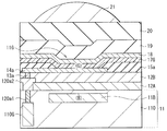
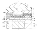
- the on-chip lens 21 is arranged so as to be shifted according to the pixel position (so-called pupil correction is performed).
- the optical axis Z of the on-chip lens 21 is arranged to be equal to the pixel central axis A, and in the end pixel, the optical axis Z of the on-chip lens 21 is the pixel central axis. It is arranged at a position shifted from A by a predetermined distance B.
- the lens position is offset so that the sensitivity becomes maximum at a certain light incident angle (incident angle ⁇ ).
- the shift amount of the on-chip lens 21 in each pixel gradually changes from the central portion toward the end portion (set according to the distance from the central portion).
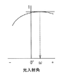
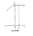
- FIG. 23A shows the light incident angle-sensitivity characteristic of the organic photoelectric conversion unit 10a in the central pixel (FIG. 23A), and FIG. 23AB shows the light incident angle-sensitivity characteristic of the inorganic photoelectric conversion unit 10b in the pixel.
- 25A shows the light incident angle-sensitivity characteristic of the organic photoelectric conversion unit 10a in the end pixel (FIG. 23B), and
- FIG. 25B shows the light incident angle-sensitivity characteristic of the inorganic photoelectric conversion unit 10b in the pixel.
- Show. 23A and 23B the sensitivity at a light incident angle of 0 ° is normalized as 1
- FIGS. 25A and 25B the sensitivity at a light incident angle ⁇ is normalized as 1.
- the illuminance E of light incident at the light incident angle ⁇ is expressed by the following equation (1), where E 0 is the illuminance on the optical axis (illuminance when the light incident angle is 0 °).
- E E 0 cos 4 ⁇ (1)
- the openings H11 and H12 are set so that the sensitivity in the central pixel (light incident angle 0 °, no lens offset) is equal to the sensitivity in the end pixel (light incident angle ⁇ , with lens offset). It is desirable that the area ratio of the respective areas S11 and S12 satisfies the following expression (2).
- S11: S12 cos 4 ⁇ : 1 (2)
- the opening area is set for each pixel (according to the pixel position) as described above.
- the organic photoelectric conversion unit 10a and the inorganic photoelectric conversion are performed for each pixel.
- the sensitivity of the organic photoelectric conversion unit 10a in each pixel is not limited to the case where the sensitivity is controlled by the opening area (the junction area of the organic photoelectric conversion layer 17 with the lower electrode 14), and has been described in the second embodiment. In such a pixel structure, it may be controlled by the area of the upper electrode 18a.
- the sensitivity control in consideration of the pupil correction of the present embodiment can be applied to each stacked structure as described in the third to fifth embodiments.
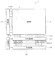
- FIG. 26 is a functional block diagram of a solid-state imaging device (solid-state imaging device 1) using the photoelectric conversion element described in the above embodiment for each pixel.
- the solid-state imaging device 1 is a CMOS image sensor and includes a pixel unit 1a as an imaging area, and includes a circuit unit 130 including, for example, a row scanning unit 131, a horizontal selection unit 133, a column scanning unit 134, and a system control unit 132. Have.
- the circuit unit 130 may be provided in the peripheral region of the pixel unit 1a or the pixel unit 1a, and may be provided in the peripheral region of the pixel unit 1a, or may be stacked with the pixel unit 1a (opposing the pixel unit 1a). May be provided).
- the pixel unit 1a has, for example, a plurality of unit pixels P (corresponding to the photoelectric conversion element 10) arranged two-dimensionally in a matrix.
- a pixel drive line Lread (specifically, a row selection line and a reset control line) is wired for each pixel row, and a vertical signal line Lsig is wired for each pixel column.
- the pixel drive line Lread transmits a drive signal for reading a signal from the pixel.
- One end of the pixel drive line Lread is connected to an output end corresponding to each row of the row scanning unit 131.
- the row scanning unit 131 includes a shift register, an address decoder, and the like, and is a pixel driving unit that drives each pixel P of the pixel unit 1a, for example, in units of rows.
- a signal output from each pixel P in the pixel row selected and scanned by the row scanning unit 131 is supplied to the horizontal selection unit 133 through each of the vertical signal lines Lsig.
- the horizontal selection unit 133 is configured by an amplifier, a horizontal selection switch, and the like provided for each vertical signal line Lsig.
- the column scanning unit 134 includes a shift register, an address decoder, and the like, and drives the horizontal selection switches in the horizontal selection unit 133 in order while scanning. By the selective scanning by the column scanning unit 134, the signal of each pixel transmitted through each of the vertical signal lines Lsig is sequentially transmitted to the horizontal signal line 135 and output to the outside through the horizontal signal line 135.
- the system control unit 132 receives a clock given from the outside, data for instructing an operation mode, and the like, and outputs data such as internal information of the solid-state imaging device 1.
- the system control unit 132 further includes a timing generator that generates various timing signals.
- the row scanning unit 131, the horizontal selection unit 133, the column scanning unit 134, and the like are based on the various timing signals generated by the timing generator. Drive control is performed.
- FIG. 27 shows a schematic configuration of the electronic apparatus 2 (camera) as an example.
- the electronic device 2 is, for example, a video camera capable of shooting a still image or a moving image, and drives the solid-state imaging device 1, the optical system (optical lens) 310, the shutter device 311, the solid-state imaging device 1 and the shutter device 311. And a signal processing unit 312.
- the optical system 310 guides image light (incident light) from a subject to the pixel unit 1 a of the solid-state imaging device 1.
- the optical system 310 may be composed of a plurality of optical lenses.
- the shutter device 311 controls the light irradiation period and the light shielding period for the solid-state imaging device 1.
- the drive unit 313 controls the transfer operation of the solid-state imaging device 1 and the shutter operation of the shutter device 311.
- the signal processing unit 312 performs various types of signal processing on the signal output from the solid-state imaging device 1.
- the video signal Dout after the signal processing is stored in a storage medium such as a memory, or is output to a monitor or the like.
- the organic photoelectric conversion unit has exemplified the case where the inter-pixel insulating film is provided on the lower electrode, and the lower electrode and the organic photoelectric conversion layer are joined at the opening.
- the insulating film is not necessarily provided.
- the above-described light incident angle-sensitivity characteristic may be set according to the area of the surface of the lower electrode on the organic photoelectric conversion layer side.
- the backside illumination type solid-state imaging device has been described as an example, but the present disclosure can be applied to a frontside illumination type.
- the photoelectric conversion element of the present disclosure does not need to include all the constituent elements described in the above-described embodiments and the like, and conversely, may include other layers.
- the present disclosure may be configured as follows. (1) Each includes a plurality of pixels having at least two first and second photoelectric conversion units stacked, The solid-state imaging device in which the rate of change of the sensitivity of each of the first and second photoelectric conversion units with respect to the light incident angle is equal for each pixel. (2) The solid-state imaging device according to (1), wherein at least a first photoelectric conversion unit of the first and second photoelectric conversion units is provided on a semiconductor substrate. (3) The solid-state imaging device according to (2), wherein the first photoelectric conversion unit includes an organic photoelectric conversion layer. (4) The first photoelectric conversion unit has a first electrode, an organic photoelectric conversion layer, and a second electrode in this order on a semiconductor substrate.
- the solid-state imaging device (2), wherein the first electrode is separated for each pixel.
- the sensitivity in the first photoelectric conversion unit is set according to a bonding area between the first electrode and the organic photoelectric conversion layer.
- the solid-state imaging device (4).
- the sensitivity in the first photoelectric conversion unit is set according to an opening area of the opening.
- the solid-state imaging device (5).
- the sensitivity in the first photoelectric conversion unit is set according to the area of the surface of the first electrode on the organic photoelectric conversion layer side.
- the solid-state imaging device (5).
- the first photoelectric conversion unit has a first electrode, an organic photoelectric conversion layer, and a second electrode in this order on a semiconductor substrate.
- the solid-state imaging device according to (2) wherein the second electrode is separated for each pixel.
- the sensitivity in the first photoelectric conversion unit is set in accordance with a bonding area between the second electrode and the organic photoelectric conversion layer.
- the first photoelectric conversion unit includes an organic photoelectric conversion layer,
- the solid state imaging device according to (2), wherein the second photoelectric conversion unit is provided in the semiconductor substrate and includes an inorganic photoelectric conversion layer.
- the solid-state imaging device wherein the organic photoelectric conversion layer and the inorganic photoelectric conversion layer as a whole include each photoelectric conversion layer of red light, green light, and blue light.
- the organic photoelectric conversion layer performs green light photoelectric conversion
- the second photoelectric conversion unit includes, as the inorganic photoelectric conversion layer, a photoelectric conversion layer that performs photoelectric conversion of blue light and a photoelectric conversion layer that performs photoelectric conversion of red light. apparatus.
- the first photoelectric conversion unit includes, as the organic photoelectric conversion layer, a photoelectric conversion layer that performs photoelectric conversion of blue light, and a photoelectric conversion layer that performs photoelectric conversion of green light,
- each of the first and second photoelectric conversion units is provided with a shorter wavelength photoelectric conversion layer on a light incident side.
- the solid-state imaging device wherein the first and second photoelectric conversion units as a whole include organic photoelectric conversion layers of red light, green light, and blue light.
- the red organic photoelectric conversion layer, the green organic photoelectric conversion layer, and the blue organic photoelectric conversion layer are provided in order from the semiconductor substrate side.
- the solid-state imaging device according to (16) above.
- the plurality of pixels are two-dimensionally arranged, In each pixel, a microlens is provided on the light incident side of the first and second photoelectric conversion units, and the optical axis of the microlens is shifted from the pixel center according to the pixel position in the two-dimensional array.
- the solid-state imaging device according to any one of (1) to (17).
- At least a first photoelectric conversion unit of the first and second photoelectric conversion units is provided on a semiconductor substrate, The solid-state imaging device according to (18), wherein the sensitivity in the first photoelectric conversion unit is set according to the pixel position.
- Each includes a plurality of pixels having at least two first and second photoelectric conversion units stacked, An electronic apparatus having a solid-state imaging device in which the rate of change of the sensitivity of each of the first and second photoelectric conversion units with respect to the light incident angle is equal to each other for each pixel.
Landscapes
- Engineering & Computer Science (AREA)
- Multimedia (AREA)
- Signal Processing (AREA)
- Physics & Mathematics (AREA)
- Electromagnetism (AREA)
- Chemical & Material Sciences (AREA)
- Inorganic Chemistry (AREA)
- Solid State Image Pick-Up Elements (AREA)
- Transforming Light Signals Into Electric Signals (AREA)
Abstract
Description
1.第1の実施の形態(半導体基板上に有機光電変換部(G)、半導体基板内に無機光電変換部(B,R)を設けた光電変換素子の例)
2.第2の実施の形態(上部電極を画素毎に分離した場合の例)
3.第3の実施の形態(有機光電変換部(G,B)および無機光電変換部(R)を積層した場合の例)
4.第4の実施の形態(有機光電変換部(R,G,B)のみを積層した場合の例)
5.第5の実施の形態(受光波長の異なる画素を並列配置させた場合の例)
6.第6の実施の形態(オンチップレンズによる瞳補正を付加した場合の例)
7.固体撮像装置の全体構成例
8.適用例(電子機器(カメラ)の例)
[構成]
図1は、本開示の第1の実施の形態に係る固体撮像装置における画素(光電変換素子10)の概略断面構成を表すものである。固体撮像装置は、詳細は後述するが、例えばCCD(Charge Coupled Device)またはCMOS(Complementary Metal Oxide Semiconductor)イメージセンサなどである。光電変換素子10では、半導体基板11の表面(受光面と反対側の面S2)側に、画素トランジスタ(後述の転送トランジスタTr1~3を含む)が形成されると共に、この面S2側に多層配線層(多層配線層51)が設けられている。
半導体基板11は、例えばn型のシリコン(Si)層110の所定の領域に、無機光電変換層11B,11Rと緑用蓄電層110Gとが埋め込まれたものである。半導体基板11には、また、有機光電変換部11Gからの電荷(電子または正孔(ホール))の伝送経路となる導電性プラグ120a1が埋設されている。本実施の形態では、この半導体基板11の裏面(面S1)が受光面となっている。半導体基板11の表面(面S2)側には、有機光電変換部11G,無機光電変換層11B,11Rのそれぞれに対応する複数の画素トランジスタ(転送トランジスタTr1~Tr3を含む)が形成されると共に、ロジック回路等からなる周辺回路が形成されている。
有機光電変換部10a(ここでは、有機光電変換部11G)は、有機半導体を用いて、選択的な波長の光(ここでは、緑色光)を吸収して、電子・ホール対を発生させる有機光電変換素子である。この有機光電変換部10a(11G)は、信号電荷を取り出すための一対の電極(下部電極14a,上部電極18)間に有機光電変換層17(17G)を挟み込んだ構成を有している。下部電極14a(第1電極)は、半導体基板11内に埋設された導電性プラグ120a1に電気的に接続されている。上部電極18(第2電極)は、例えば固体撮像装置の周縁部において、図示しないコンタクト部を介して多層配線層51内の配線51aに接続されており、これにより電荷(ここではホール)が排出されるようになっている。
上記のような光電変換素子10は、例えば次のようにして製造することができる。図9~図14は、光電変換素子10の製造方法を工程順に表したものである。但し、ここでは、光電変換素子10の要部構成のみを図示し、半導体基板11の面S1側に、有機光電変換部11Gを形成する際の手順について具体的に説明する。
本実施の形態の光電変換素子10では、例えば固体撮像装置の画素として、次のようにして信号電荷が取得される。即ち、光電変換素子10に、オンチップレンズ21を介して光が入射すると、この入射光は、有機光電変換部10a(11G)、無機光電変換部10b(無機光電変換層11B,11R)の順に通過し、その通過過程において赤、緑、青の色光毎に光電変換される。
図15Aおよび図15Bは、本実施の形態の比較例に係る光電変換素子の光入射角-感度特性を示すものである。図15Aは、有機光電変換部の光入射角-感度特性を、図15Bは、無機光電変換部の光入射角-感度特性をそれぞれ示す。尚、比較例においても、半導体基板内に無機光電変換部が形成され、有機光電変換部は半導体基板上に形成されているものとする。
図18は、第2の実施の形態の光電変換素子の要部構成を表したものである。上記第1の実施の形態では、下部電極14aを画素毎に分離した構成において、下部電極14aから信号電荷の取り出しを行う場合について説明したが、上部電極18aを画素毎に分離した構成としてもよい。この場合、上部電極18aから信号電荷の取り出しを行うことができ、下部電極14bについては、各画素に共通して設けることができる。
図19は、第3の実施の形態の光電変換素子の要部構成を表したものである。上記第1の実施の形態では、有機光電変換部10aに、1つの有機光電変換層17G、無機光電変換部10bに、2つの無機光電変換層11B,11Rを設けたが、各光電変換部に積層される光電変換層数の組み合わせは、これに限定されない。即ち、有機光電変換部10aに、2つの有機光電変換層、無機光電変換部10bに、1つの無機光電変換層が設けられていてもよい。例えば、有機光電変換部10aとして、青色光の光電変換を行う有機光電変換部11Bと、緑色光の光電変換を行う有機光電変換部11Gとが設けられ、無機光電変換部10bに、赤色光の光電変換を行う無機光電変換層11Rが設けられている。
図20は、第4の実施の形態の光電変換素子の要部構成を表したものである。上記第1および第2の実施の形態では、半導体基板11上に有機光電変換部10a、半導体基板11内に無機光電変換部10bが形成されている場合について説明したが、有機光電変換部10aのみからなる構成であってもよい。但し、この場合、有機光電変換部10aが2以上の有機光電変換部、例えば、R,G,Bの3色の光をそれぞれ光電変換する有機光電変換部11R,11G,11Bからなる。
図21Aおよび図21Bは、第5の実施の形態の光電変換素子の要部構成を表したものである。上記第1の実施の形態では、1つの画素内に、R,G,Bの各色を光電変換する3つの光電変換層を積層した場合について説明したが、必ずしもこれらの3層を同一画素内に配置しなくともよい。例えば、有機光電変換部10aとして有機光電変換部11G、無機光電変換部10bとして無機光電変換層11Bをそれぞれ有する画素A(図21A)と、有機光電変換部10aとして有機光電変換部11G、無機光電変換部10bとして無機光電変換層11Rをそれぞれ有する画素B(図21B)とが、2次元配列していてもよい。画素Aでは、半導体基板11内の比較的浅い領域に無機光電変換層11Bが形成されている一方、画素Bでは、半導体基板11内の比較的深い領域に無機光電変換層11Rが形成されている。これらの画素A,Bの2次元配列は、例えば図22に示したように、千鳥格子状となっている。
図23Aおよび図23Bは、第6の実施の形態の光電変換素子の要部構成を表したものである。図23Aは、後述の固体撮像装置において、画素領域(後述の画素部1a,チップ)の中央部に配置された画素、図23Bは、画素領域の端部(中央部から離れた領域)に配置された画素にそれぞれ対応している。本実施の形態においても、上記第1の実施の形態と同様、画素毎に、有機光電変換部10aの光入射角-感度特性が、無機光電変換部10bの光入射角-感度特性と同等となるように設定されている。ところで、複数の画素が2次元配置された固体撮像装置では、その画素位置に応じて光入射角が異なる。このため、本実施の形態では、オンチップレンズ21が、画素位置に応じてシフトして配置されている(いわゆる瞳補正がなされている)。具体的には、中央部の画素では、オンチップレンズ21の光軸Zが画素中心軸Aに等しくなるように配置され、端部の画素では、オンチップレンズ21の光軸Zが画素中心軸Aから所定の距離Bだけシフトした位置に配置されている。即ち、端部の画素では、ある光入射角(入射角ω)において感度が最大となるようにレンズ位置がオフセットされている。尚、図示は省略するが、各画素におけるオンチップレンズ21のシフト量は、中央部から端部に向かって徐々に変化している(中央部からの距離に応じて設定されている)。
E=E0cos4θ ………(1)
S11:S12=cos4ω:1 ………(2)
図26は、上記実施の形態において説明した光電変換素子を各画素に用いた固体撮像装置(固体撮像装置1)の機能ブロック図である。この固体撮像装置1は、CMOSイメージセンサであり、撮像エリアとしての画素部1aを有すると共に、例えば行走査部131、水平選択部133、列走査部134およびシステム制御部132からなる回路部130を有している。この画素部1aの周辺領域あるいは画素部1aと積層されて、回路部130は、画素部1aの周辺領域に設けられていてもよいし、画素部1aと積層されて(画素部1aに対向する領域に)設けられていてもよい。
上述の固体撮像装置1は、例えばデジタルスチルカメラやビデオカメラ等のカメラシステムや、撮像機能を有する携帯電話など、撮像機能を備えたあらゆるタイプの電子機器に適用することができる。図27に、その一例として、電子機器2(カメラ)の概略構成を示す。この電子機器2は、例えば静止画または動画を撮影可能なビデオカメラであり、固体撮像装置1と、光学系(光学レンズ)310と、シャッタ装置311と、固体撮像装置1およびシャッタ装置311を駆動する駆動部313と、信号処理部312とを有する。
(1)
各々が、積層された少なくとも2つの第1および第2の光電変換部を有する複数の画素を備え、
前記画素毎に、前記第1および第2の光電変換部のそれぞれの感度の光入射角に対する変化率が互いに等しくなっている
固体撮像装置。
(2)
前記第1および第2の光電変換部のうちの少なくとも第1の光電変換部は、半導体基板上に設けられている
上記(1)に記載の固体撮像装置。
(3)
前記第1の光電変換部は有機光電変換層を含む
上記(2)に記載の固体撮像装置。
(4)
前記第1の光電変換部は、半導体基板上に、第1電極、有機光電変換層および第2電極をこの順に有し、
前記第1電極は前記画素毎に分離されている
上記(2)に記載の固体撮像装置。
(5)
前記第1の光電変換部における前記感度は、前記第1電極と前記有機光電変換層との接合面積に応じて設定されている
上記(4)に記載の固体撮像装置。
(6)
前記第1電極と前記有機光電変換層との間に設けられると共に、前記第1電極に対向して開口部を有する絶縁膜を更に有し、
前記第1の光電変換部における前記感度は、前記開口部の開口面積に応じて設定されている
上記(5)に記載の固体撮像装置。
(7)
前記第1の光電変換部における前記感度は、前記第1電極の前記有機光電変換層側の面の面積に応じて設定されている
上記(5)に記載の固体撮像装置。
(8)
前記第1の光電変換部は、半導体基板上に、第1電極、有機光電変換層および第2電極をこの順に有し、
前記第2電極は前記画素毎に分離されている
上記(2)に記載の固体撮像装置。
(9)
前記第1の光電変換部における前記感度は、前記第2電極と前記有機光電変換層との接合面積に応じて設定されている
上記(8)に記載の固体撮像装置。
(10)
前記第1の光電変換部は有機光電変換層を含み、
前記第2の光電変換部は、前記半導体基板内に設けられると共に無機光電変換層を含む
上記(2)に記載の固体撮像装置。
(11)
前記有機光電変換層および前記無機光電変換層が全体として、赤色光、緑色光および青色光の各光電変換層を含む
上記(10)に記載の固体撮像装置。
(12)
前記第1の光電変換部では、前記有機光電変換層が緑色光の光電変換を行い、
前記第2の光電変換部は、前記無機光電変換層として、青色光の光電変換を行う光電変換層と、赤色光の光電変換を行う光電変換層とを含む
上記(11)に記載の固体撮像装置。
(13)
前記第1の光電変換部は、前記有機光電変換層として、青色光の光電変換を行う光電変換層と、緑色光の光電変換を行う光電変換層とを含み、
前記第2の光電変換部では、前記無機光電変換層が赤色光の光電変換を行う
上記(11)に記載の固体撮像装置。
(14)
前記第1および第2の光電変換部のそれぞれにおいて、光入射側に、より短波長の光電変換層が設けられている
上記(11)に記載の固体撮像装置。
(15)
前記第1および第2の光電変換部の両方が、前記半導体基板上に設けられると共に1または2以上の有機光電変換層を含む
上記(2)に記載の固体撮像装置。
(16)
前記第1および第2の光電変換部が全体として、赤色光、緑色光および青色光の有機光電変換層を含む
上記(15)に記載の固体撮像装置。
(17)
前記半導体基板側から順に、赤色有機光電変換層、緑色有機光電変換層および青色有機光電変換層が設けられている
上記(16)に記載の固体撮像装置。
(18)
前記複数の画素は2次元配列され、
各画素では、前記第1および第2の光電変換部よりも光入射側に、マイクロレンズが設けられ、かつ
前記マイクロレンズは、前記2次元配列における画素位置に応じて光軸が画素中心からシフトして配置されている
上記(1)~(17)のいずれかに記載の固体撮像装置。
(19)
前記第1および第2の光電変換部のうちの少なくとも第1の光電変換部は、半導体基板上に設けられ、
前記第1の光電変換部における前記感度は、前記画素位置に応じて設定されている
上記(18)に記載の固体撮像装置。
(20)
各々が、積層された少なくとも2つの第1および第2の光電変換部を有する複数の画素を備え、
前記画素毎に、前記第1および第2の光電変換部のそれぞれの感度の光入射角に対する変化率が互いに等しくなっている
固体撮像装置を有する電子機器。
Claims (20)
- 各々が、積層された少なくとも2つの第1および第2の光電変換部を有する複数の画素を備え、
前記画素毎に、前記第1および第2の光電変換部のそれぞれの感度の光入射角に対する変化率が互いに等しくなっている
固体撮像装置。 - 前記第1および第2の光電変換部のうちの少なくとも第1の光電変換部は、半導体基板上に設けられている
請求項1に記載の固体撮像装置。 - 前記第1の光電変換部は有機光電変換層を含む
請求項2に記載の固体撮像装置。 - 前記第1の光電変換部は、半導体基板上に、第1電極、有機光電変換層および第2電極をこの順に有し、
前記第1電極は前記画素毎に分離されている
請求項2に記載の固体撮像装置。 - 前記第1の光電変換部における前記感度は、前記第1電極と前記有機光電変換層との接合面積に応じて設定されている
請求項4に記載の固体撮像装置。 - 前記第1電極と前記有機光電変換層との間に設けられると共に、前記第1電極に対向して開口部を有する絶縁膜を更に有し、
前記第1の光電変換部における前記感度は、前記開口部の開口面積に応じて設定されている
請求項5に記載の固体撮像装置。 - 前記第1の光電変換部における前記感度は、前記第1電極の前記有機光電変換層側の面の面積に応じて設定されている
請求項5に記載の固体撮像装置。 - 前記第1の光電変換部は、半導体基板上に、第1電極、有機光電変換層および第2電極をこの順に有し、
前記第2電極は前記画素毎に分離されている
請求項2に記載の固体撮像装置。 - 前記第1の光電変換部における前記感度は、前記第2電極と前記有機光電変換層との接合面積に応じて設定されている
請求項8に記載の固体撮像装置。 - 前記第1の光電変換部は有機光電変換層を含み、
前記第2の光電変換部は、前記半導体基板内に設けられると共に無機光電変換層を含む
請求項2に記載の固体撮像装置。 - 前記有機光電変換層および前記無機光電変換層が全体として、赤色光、緑色光および青色光の各光電変換層を含む
請求項10に記載の固体撮像装置。 - 前記第1の光電変換部では、前記有機光電変換層が緑色光の光電変換を行い、
前記第2の光電変換部は、前記無機光電変換層として、青色光の光電変換を行う光電変換層と、赤色光の光電変換を行う光電変換層とを含む
請求項11に記載の固体撮像装置。 - 前記第1の光電変換部は、前記有機光電変換層として、青色光の光電変換を行う光電変換層と、緑色光の光電変換を行う光電変換層とを含み、
前記第2の光電変換部では、前記無機光電変換層が赤色光の光電変換を行う
請求項11に記載の固体撮像装置。 - 前記第1および第2の光電変換部のそれぞれにおいて、光入射側に、より短波長の光電変換層が設けられている
請求項11に記載の固体撮像装置。 - 前記第1および第2の光電変換部の両方が、前記半導体基板上に設けられると共に1または2以上の有機光電変換層を含む
請求項2に記載の固体撮像装置。 - 前記第1および第2の光電変換部が全体として、赤色光、緑色光および青色光の有機光電変換層を含む
請求項15に記載の固体撮像装置。 - 前記半導体基板側から順に、赤色有機光電変換層、緑色有機光電変換層および青色有機光電変換層が設けられている
請求項16に記載の固体撮像装置。 - 前記複数の画素は2次元配列され、
各画素では、前記第1および第2の光電変換部よりも光入射側に、マイクロレンズが設けられ、かつ
前記マイクロレンズは、前記2次元配列における画素位置に応じて光軸が画素中心からシフトして配置されている
請求項1に記載の固体撮像装置。 - 前記第1および第2の光電変換部のうちの少なくとも第1の光電変換部は、半導体基板上に設けられ、
前記第1の光電変換部における前記感度は、前記画素位置に応じて設定されている
請求項18に記載の固体撮像装置。 - 各々が、積層された少なくとも2つの第1および第2の光電変換部を有する複数の画素を備え、
前記画素毎に、前記第1および第2の光電変換部のそれぞれの感度の光入射角に対する変化率が互いに等しくなっている
固体撮像装置を有する電子機器。
Priority Applications (3)
| Application Number | Priority Date | Filing Date | Title |
|---|---|---|---|
| JP2014530526A JPWO2014027588A1 (ja) | 2012-08-14 | 2013-08-07 | 固体撮像装置および電子機器 |
| US14/420,002 US9601547B2 (en) | 2012-08-14 | 2013-08-07 | Solid-state image pickup device and electronic apparatus |
| US15/443,663 US10096657B2 (en) | 2012-08-14 | 2017-02-27 | Solid-state image pickup device and electronic apparatus |
Applications Claiming Priority (2)
| Application Number | Priority Date | Filing Date | Title |
|---|---|---|---|
| JP2012-179688 | 2012-08-14 | ||
| JP2012179688 | 2012-08-14 |
Related Child Applications (2)
| Application Number | Title | Priority Date | Filing Date |
|---|---|---|---|
| US14/420,002 A-371-Of-International US9601547B2 (en) | 2012-08-14 | 2013-08-07 | Solid-state image pickup device and electronic apparatus |
| US15/443,663 Continuation US10096657B2 (en) | 2012-08-14 | 2017-02-27 | Solid-state image pickup device and electronic apparatus |
Publications (1)
| Publication Number | Publication Date |
|---|---|
| WO2014027588A1 true WO2014027588A1 (ja) | 2014-02-20 |
Family
ID=50685564
Family Applications (1)
| Application Number | Title | Priority Date | Filing Date |
|---|---|---|---|
| PCT/JP2013/071338 Ceased WO2014027588A1 (ja) | 2012-08-14 | 2013-08-07 | 固体撮像装置および電子機器 |
Country Status (3)
| Country | Link |
|---|---|
| US (2) | US9601547B2 (ja) |
| JP (1) | JPWO2014027588A1 (ja) |
| WO (1) | WO2014027588A1 (ja) |
Cited By (10)
| Publication number | Priority date | Publication date | Assignee | Title |
|---|---|---|---|---|
| KR20160025320A (ko) * | 2014-08-27 | 2016-03-08 | 삼성전자주식회사 | 적층형 촬상 소자 |
| WO2017110515A1 (ja) * | 2015-12-24 | 2017-06-29 | ソニー株式会社 | 撮像装置、電子機器 |
| WO2017163559A1 (ja) * | 2016-03-23 | 2017-09-28 | ソニー株式会社 | 固体撮像素子及び電子機器 |
| WO2019044103A1 (ja) * | 2017-08-31 | 2019-03-07 | ソニーセミコンダクタソリューションズ株式会社 | 撮像素子、積層型撮像素子及び固体撮像装置 |
| JP2019165250A (ja) * | 2019-06-10 | 2019-09-26 | キヤノン株式会社 | 光電変換装置 |
| WO2019220897A1 (ja) * | 2018-05-18 | 2019-11-21 | ソニーセミコンダクタソリューションズ株式会社 | 撮像素子および電子機器並びに撮像素子の駆動方法 |
| WO2019240121A1 (ja) | 2018-06-15 | 2019-12-19 | ソニー株式会社 | 固体撮像素子、固体撮像装置、電子機器、及び、固体撮像素子の製造方法 |
| JP2019216256A (ja) * | 2014-05-13 | 2019-12-19 | ソニーセミコンダクタソリューションズ株式会社 | 光電変換膜、固体撮像素子、および電子機器 |
| WO2021100605A1 (ja) * | 2019-11-20 | 2021-05-27 | ソニーセミコンダクタソリューションズ株式会社 | 固体撮像装置および固体撮像装置の製造方法 |
| JP2022173277A (ja) * | 2014-09-26 | 2022-11-18 | 株式会社半導体エネルギー研究所 | 撮像装置 |
Families Citing this family (14)
| Publication number | Priority date | Publication date | Assignee | Title |
|---|---|---|---|---|
| JPWO2014027588A1 (ja) * | 2012-08-14 | 2016-07-25 | ソニー株式会社 | 固体撮像装置および電子機器 |
| JP5777825B2 (ja) * | 2012-12-05 | 2015-09-09 | 富士フイルム株式会社 | 撮像装置、異常斜め入射光検出方法及びプログラム、並びに記録媒体 |
| WO2014087804A1 (ja) * | 2012-12-07 | 2014-06-12 | 富士フイルム株式会社 | 撮像装置、画像処理方法及びプログラム |
| JP5802858B2 (ja) * | 2013-03-05 | 2015-11-04 | 富士フイルム株式会社 | 撮像装置、画像処理装置、画像処理方法及びプログラム |
| KR102192570B1 (ko) * | 2014-07-30 | 2020-12-17 | 삼성전자주식회사 | 컬러 필터들 사이에 위치하는 금속 패턴을 포함하는 이미지 센서 |
| JP6541313B2 (ja) * | 2014-07-31 | 2019-07-10 | キヤノン株式会社 | 光電変換装置、及び撮像システム |
| JP6429525B2 (ja) * | 2014-07-31 | 2018-11-28 | キヤノン株式会社 | 撮像装置、撮像システムおよび撮像装置の製造方法 |
| KR102395050B1 (ko) * | 2015-02-05 | 2022-05-04 | 삼성전자주식회사 | 광전자 소자 및 이를 포함하는 이미지 센서와 전자 장치 |
| JP2017208496A (ja) * | 2016-05-20 | 2017-11-24 | ソニー株式会社 | 固体撮像装置、及び、電子機器 |
| JP2018060910A (ja) * | 2016-10-05 | 2018-04-12 | ソニーセミコンダクタソリューションズ株式会社 | 固体撮像素子および固体撮像装置 |
| KR102514047B1 (ko) | 2018-02-20 | 2023-03-24 | 삼성전자주식회사 | 복수의 기능이 통합된 이미지 센서 및 이를 포함하는 이미지 센서 모듈 |
| CN112385044B (zh) | 2018-07-17 | 2024-09-17 | 索尼半导体解决方案公司 | 摄像元件、层叠型摄像元件和固态摄像装置 |
| US12235392B2 (en) * | 2019-03-06 | 2025-02-25 | Sony Semiconductor Solutions Corporation | Sensor and distance measurement apparatus having an avalanche photodiode and on-chip lens |
| KR20250009152A (ko) * | 2023-07-10 | 2025-01-17 | 삼성전자주식회사 | 이미지 픽셀 및 그것을 포함하는 이미지 센서 장치 |
Citations (4)
| Publication number | Priority date | Publication date | Assignee | Title |
|---|---|---|---|---|
| WO2008010292A1 (en) * | 2006-07-21 | 2008-01-24 | Renesas Technology Corp. | Photoelectric conversion device and imaging device |
| JP2010067828A (ja) * | 2008-09-11 | 2010-03-25 | Fujifilm Corp | 固体撮像素子及び撮像装置 |
| JP2010129548A (ja) * | 2008-11-25 | 2010-06-10 | Sony Corp | 固体撮像装置および電子機器 |
| JP2012084873A (ja) * | 2011-09-20 | 2012-04-26 | Dainippon Printing Co Ltd | 固体撮像素子の製造方法 |
Family Cites Families (5)
| Publication number | Priority date | Publication date | Assignee | Title |
|---|---|---|---|---|
| JP5564847B2 (ja) | 2009-07-23 | 2014-08-06 | ソニー株式会社 | 固体撮像装置とその製造方法、及び電子機器 |
| JP5671789B2 (ja) * | 2009-08-10 | 2015-02-18 | ソニー株式会社 | 固体撮像装置とその製造方法および撮像装置 |
| JP5509846B2 (ja) * | 2009-12-28 | 2014-06-04 | ソニー株式会社 | 固体撮像装置とその製造方法、及び電子機器 |
| JP2012129358A (ja) * | 2010-12-15 | 2012-07-05 | Toshiba Corp | 固体撮像装置及びその製造方法 |
| JPWO2014027588A1 (ja) * | 2012-08-14 | 2016-07-25 | ソニー株式会社 | 固体撮像装置および電子機器 |
-
2013
- 2013-08-07 JP JP2014530526A patent/JPWO2014027588A1/ja active Pending
- 2013-08-07 WO PCT/JP2013/071338 patent/WO2014027588A1/ja not_active Ceased
- 2013-08-07 US US14/420,002 patent/US9601547B2/en not_active Expired - Fee Related
-
2017
- 2017-02-27 US US15/443,663 patent/US10096657B2/en active Active
Patent Citations (4)
| Publication number | Priority date | Publication date | Assignee | Title |
|---|---|---|---|---|
| WO2008010292A1 (en) * | 2006-07-21 | 2008-01-24 | Renesas Technology Corp. | Photoelectric conversion device and imaging device |
| JP2010067828A (ja) * | 2008-09-11 | 2010-03-25 | Fujifilm Corp | 固体撮像素子及び撮像装置 |
| JP2010129548A (ja) * | 2008-11-25 | 2010-06-10 | Sony Corp | 固体撮像装置および電子機器 |
| JP2012084873A (ja) * | 2011-09-20 | 2012-04-26 | Dainippon Printing Co Ltd | 固体撮像素子の製造方法 |
Cited By (27)
| Publication number | Priority date | Publication date | Assignee | Title |
|---|---|---|---|---|
| JP2019216256A (ja) * | 2014-05-13 | 2019-12-19 | ソニーセミコンダクタソリューションズ株式会社 | 光電変換膜、固体撮像素子、および電子機器 |
| KR20160025320A (ko) * | 2014-08-27 | 2016-03-08 | 삼성전자주식회사 | 적층형 촬상 소자 |
| KR102296736B1 (ko) | 2014-08-27 | 2021-08-31 | 삼성전자주식회사 | 적층형 촬상 소자 |
| JP2022173277A (ja) * | 2014-09-26 | 2022-11-18 | 株式会社半導体エネルギー研究所 | 撮像装置 |
| WO2017110515A1 (ja) * | 2015-12-24 | 2017-06-29 | ソニー株式会社 | 撮像装置、電子機器 |
| JPWO2017110515A1 (ja) * | 2015-12-24 | 2018-10-11 | ソニー株式会社 | 撮像装置、電子機器 |
| US10546898B2 (en) | 2015-12-24 | 2020-01-28 | Sony Corporation | Imaging apparatus and electronic device |
| WO2017163559A1 (ja) * | 2016-03-23 | 2017-09-28 | ソニー株式会社 | 固体撮像素子及び電子機器 |
| CN109075179A (zh) * | 2016-03-23 | 2018-12-21 | 索尼公司 | 固态成像元件和电子设备 |
| CN109075179B (zh) * | 2016-03-23 | 2024-02-13 | 索尼公司 | 固态成像元件和电子设备 |
| US11411034B2 (en) | 2016-03-23 | 2022-08-09 | Sony Corporation | Solid-state imaging device and electronic apparatus |
| US10651222B2 (en) | 2016-03-23 | 2020-05-12 | Sony Corporation | Solid-state imaging device and electronic apparatus |
| JPWO2019044103A1 (ja) * | 2017-08-31 | 2020-10-15 | ソニーセミコンダクタソリューションズ株式会社 | 撮像素子、積層型撮像素子及び固体撮像装置 |
| US11621290B2 (en) | 2017-08-31 | 2023-04-04 | Sony Semiconductor Solutions Corporation | Imaging element, laminated imaging element, and solid-state imaging device |
| US12538604B2 (en) | 2017-08-31 | 2026-01-27 | Sony Semiconductor Solutions Corp. | Imaging element, laminated imaging element, and solid-state imaging device |
| WO2019044103A1 (ja) * | 2017-08-31 | 2019-03-07 | ソニーセミコンダクタソリューションズ株式会社 | 撮像素子、積層型撮像素子及び固体撮像装置 |
| JP7164532B2 (ja) | 2017-08-31 | 2022-11-01 | ソニーセミコンダクタソリューションズ株式会社 | 撮像素子、積層型撮像素子及び固体撮像装置 |
| US11387279B2 (en) | 2018-05-18 | 2022-07-12 | Sony Semiconductor Solutions Corporation | Imaging element, electronic apparatus, and method of driving imaging element |
| WO2019220897A1 (ja) * | 2018-05-18 | 2019-11-21 | ソニーセミコンダクタソリューションズ株式会社 | 撮像素子および電子機器並びに撮像素子の駆動方法 |
| JP7242655B2 (ja) | 2018-05-18 | 2023-03-20 | ソニーセミコンダクタソリューションズ株式会社 | 撮像素子の駆動方法 |
| JPWO2019220897A1 (ja) * | 2018-05-18 | 2021-06-17 | ソニーセミコンダクタソリューションズ株式会社 | 撮像素子および電子機器並びに撮像素子の駆動方法 |
| WO2019240121A1 (ja) | 2018-06-15 | 2019-12-19 | ソニー株式会社 | 固体撮像素子、固体撮像装置、電子機器、及び、固体撮像素子の製造方法 |
| US11974444B2 (en) | 2018-06-15 | 2024-04-30 | Sony Corporation | Solid-state image sensor, solid-state imaging device, electronic apparatus, and method of manufacturing solid-state image sensor |
| JP2019165250A (ja) * | 2019-06-10 | 2019-09-26 | キヤノン株式会社 | 光電変換装置 |
| WO2021100605A1 (ja) * | 2019-11-20 | 2021-05-27 | ソニーセミコンダクタソリューションズ株式会社 | 固体撮像装置および固体撮像装置の製造方法 |
| JP7615047B2 (ja) | 2019-11-20 | 2025-01-16 | ソニーセミコンダクタソリューションズ株式会社 | 固体撮像装置および固体撮像装置の製造方法 |
| JPWO2021100605A1 (ja) * | 2019-11-20 | 2021-05-27 |
Also Published As
| Publication number | Publication date |
|---|---|
| JPWO2014027588A1 (ja) | 2016-07-25 |
| US20150187843A1 (en) | 2015-07-02 |
| US10096657B2 (en) | 2018-10-09 |
| US9601547B2 (en) | 2017-03-21 |
| US20170170240A1 (en) | 2017-06-15 |
Similar Documents
| Publication | Publication Date | Title |
|---|---|---|
| WO2014027588A1 (ja) | 固体撮像装置および電子機器 | |
| US9614010B2 (en) | Solid-state image sensing device having an organic photoelectric conversion section fills a depression section and solid-state image pickup unit including same | |
| JP6136663B2 (ja) | 固体撮像素子およびその製造方法、並びに電子機器 | |
| JP5780402B2 (ja) | 半導体素子、半導体素子の製造方法、固体撮像装置および電子機器 | |
| US9219100B2 (en) | Semiconductor device and solid-state image pickup unit | |
| WO2014007132A1 (ja) | 固体撮像装置およびその製造方法、並びに電子機器 | |
| JP5032954B2 (ja) | カラー撮像装置 | |
| JP2013183056A (ja) | 光電変換素子、光電変換素子の製造方法、固体撮像装置および電子機器 | |
| JP2014078673A (ja) | 固体撮像装置および固体撮像装置の製造方法ならびに電子機器 | |
| US20140077324A1 (en) | Solid-state image pickup device, method of manufacturing solid-state image pickup device, and electronic apparatus | |
| WO2014021177A1 (ja) | 半導体素子、半導体素子の製造方法、固体撮像装置、および電子機器 | |
| JP2014011392A (ja) | 固体撮像装置及びその製造方法、電子機器 | |
| WO2013111676A1 (ja) | 光電変換素子、光電変換素子の製造方法、固体撮像装置および電子機器 | |
| WO2013164948A1 (ja) | 固体撮像装置及びその製造方法、電子機器 | |
| WO2017169231A1 (ja) | 撮像素子および電子機器 | |
| WO2017061176A1 (ja) | 固体撮像素子および固体撮像素子の製造方法 | |
| WO2016190217A1 (ja) | 光電変換素子および固体撮像装置ならびに電子機器 |
Legal Events
| Date | Code | Title | Description |
|---|---|---|---|
| 121 | Ep: the epo has been informed by wipo that ep was designated in this application |
Ref document number: 13879535 Country of ref document: EP Kind code of ref document: A1 |
|
| ENP | Entry into the national phase |
Ref document number: 2014530526 Country of ref document: JP Kind code of ref document: A |
|
| WWE | Wipo information: entry into national phase |
Ref document number: 14420002 Country of ref document: US |
|
| NENP | Non-entry into the national phase |
Ref country code: DE |
|
| 122 | Ep: pct application non-entry in european phase |
Ref document number: 13879535 Country of ref document: EP Kind code of ref document: A1 |