WO2014024692A1 - 電源平滑用lcフィルタの等価回路モデルの導出方法 - Google Patents
電源平滑用lcフィルタの等価回路モデルの導出方法 Download PDFInfo
- Publication number
- WO2014024692A1 WO2014024692A1 PCT/JP2013/070190 JP2013070190W WO2014024692A1 WO 2014024692 A1 WO2014024692 A1 WO 2014024692A1 JP 2013070190 W JP2013070190 W JP 2013070190W WO 2014024692 A1 WO2014024692 A1 WO 2014024692A1
- Authority
- WO
- WIPO (PCT)
- Prior art keywords
- equivalent circuit
- circuit model
- choke coil
- model
- smoothing capacitor
- Prior art date
- Legal status (The legal status is an assumption and is not a legal conclusion. Google has not performed a legal analysis and makes no representation as to the accuracy of the status listed.)
- Ceased
Links
Images





Classifications
-
- H—ELECTRICITY
- H02—GENERATION; CONVERSION OR DISTRIBUTION OF ELECTRIC POWER
- H02M—APPARATUS FOR CONVERSION BETWEEN AC AND AC, BETWEEN AC AND DC, OR BETWEEN DC AND DC, AND FOR USE WITH MAINS OR SIMILAR POWER SUPPLY SYSTEMS; CONVERSION OF DC OR AC INPUT POWER INTO SURGE OUTPUT POWER; CONTROL OR REGULATION THEREOF
- H02M1/00—Details of apparatus for conversion
- H02M1/14—Arrangements for reducing ripples from DC input or output
-
- G—PHYSICS
- G06—COMPUTING OR CALCULATING; COUNTING
- G06F—ELECTRIC DIGITAL DATA PROCESSING
- G06F30/00—Computer-aided design [CAD]
- G06F30/30—Circuit design
- G06F30/36—Circuit design at the analogue level
-
- G—PHYSICS
- G06—COMPUTING OR CALCULATING; COUNTING
- G06F—ELECTRIC DIGITAL DATA PROCESSING
- G06F30/00—Computer-aided design [CAD]
- G06F30/30—Circuit design
- G06F30/36—Circuit design at the analogue level
- G06F30/367—Design verification, e.g. using simulation, simulation program with integrated circuit emphasis [SPICE], direct methods or relaxation methods
-
- H—ELECTRICITY
- H02—GENERATION; CONVERSION OR DISTRIBUTION OF ELECTRIC POWER
- H02M—APPARATUS FOR CONVERSION BETWEEN AC AND AC, BETWEEN AC AND DC, OR BETWEEN DC AND DC, AND FOR USE WITH MAINS OR SIMILAR POWER SUPPLY SYSTEMS; CONVERSION OF DC OR AC INPUT POWER INTO SURGE OUTPUT POWER; CONTROL OR REGULATION THEREOF
- H02M3/00—Conversion of DC power input into DC power output
- H02M3/02—Conversion of DC power input into DC power output without intermediate conversion into AC
- H02M3/04—Conversion of DC power input into DC power output without intermediate conversion into AC by static converters
- H02M3/10—Conversion of DC power input into DC power output without intermediate conversion into AC by static converters using discharge tubes with control electrode or semiconductor devices with control electrode
- H02M3/145—Conversion of DC power input into DC power output without intermediate conversion into AC by static converters using discharge tubes with control electrode or semiconductor devices with control electrode using devices of a triode or transistor type requiring continuous application of a control signal
- H02M3/155—Conversion of DC power input into DC power output without intermediate conversion into AC by static converters using discharge tubes with control electrode or semiconductor devices with control electrode using devices of a triode or transistor type requiring continuous application of a control signal using semiconductor devices only
- H02M3/156—Conversion of DC power input into DC power output without intermediate conversion into AC by static converters using discharge tubes with control electrode or semiconductor devices with control electrode using devices of a triode or transistor type requiring continuous application of a control signal using semiconductor devices only with automatic control of output voltage or current, e.g. switching regulators
- H02M3/158—Conversion of DC power input into DC power output without intermediate conversion into AC by static converters using discharge tubes with control electrode or semiconductor devices with control electrode using devices of a triode or transistor type requiring continuous application of a control signal using semiconductor devices only with automatic control of output voltage or current, e.g. switching regulators including plural semiconductor devices as final control devices for a single load
- H02M3/1588—Conversion of DC power input into DC power output without intermediate conversion into AC by static converters using discharge tubes with control electrode or semiconductor devices with control electrode using devices of a triode or transistor type requiring continuous application of a control signal using semiconductor devices only with automatic control of output voltage or current, e.g. switching regulators including plural semiconductor devices as final control devices for a single load comprising at least one synchronous rectifier element
-
- Y—GENERAL TAGGING OF NEW TECHNOLOGICAL DEVELOPMENTS; GENERAL TAGGING OF CROSS-SECTIONAL TECHNOLOGIES SPANNING OVER SEVERAL SECTIONS OF THE IPC; TECHNICAL SUBJECTS COVERED BY FORMER USPC CROSS-REFERENCE ART COLLECTIONS [XRACs] AND DIGESTS
- Y02—TECHNOLOGIES OR APPLICATIONS FOR MITIGATION OR ADAPTATION AGAINST CLIMATE CHANGE
- Y02B—CLIMATE CHANGE MITIGATION TECHNOLOGIES RELATED TO BUILDINGS, e.g. HOUSING, HOUSE APPLIANCES OR RELATED END-USER APPLICATIONS
- Y02B70/00—Technologies for an efficient end-user side electric power management and consumption
- Y02B70/10—Technologies improving the efficiency by using switched-mode power supplies [SMPS], i.e. efficient power electronics conversion e.g. power factor correction or reduction of losses in power supplies or efficient standby modes
Definitions
- the present invention relates to a derivation method for deriving an equivalent circuit model of a power source smoothing LC filter composed of a choke coil and a smoothing capacitor for stabilizing the output voltage of a direct current stabilized power circuit.
- Non-Patent Document 1 the buck converter PWM (Pulse Width Modulation) switch blocks, divided into LC filter block and the constant voltage control unit blocks, seeking a transfer function X LC of divided LC filter block.
- An input / output characteristic of the power supply smoothing LC filter is simulated by the obtained transfer function XLC to derive an equivalent circuit model of the power supply smoothing LC filter.
- the equivalent circuit model of the power supply smoothing LC filter can be derived from the equivalent circuit models of the inductor and the capacitor constituting the LC filter.
- Patent Document 1 an RC circuit shown in FIG. 1A and a circuit that can be simulated in the time domain using a frequency-independent resistor (R), capacitance (C), and inductance (L) are shown.
- One of the RL circuit shown in FIG. 2B and the RCL circuit shown in FIG. 2C is formed as an equivalent circuit model of MLCC (Multi-Layer Ceramic Capacitor). Then, an evaluation function for determining the accuracy of the formed equivalent circuit model is synthesized, and a circuit constant is determined by minimizing the synthesized evaluation function.
- MLCC Multi-Layer Ceramic Capacitor
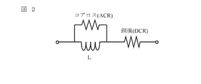
- Non-Patent Document 2 discloses a model in which a copper loss resistance DCR is connected in series to a parallel circuit of an inductance L and a core loss resistance ACR shown in FIG. 2 as an equivalent circuit model of an inductor. The same document describes which factor of the inductor represented by the equivalent circuit model affects the voltage conversion efficiency.
- the power supply disclosed in the conventional non-patent document 1 described above since the characteristics of the choke coil constituting the DC stabilized power supply circuit depend on the output current of the power supply circuit and the smoothing capacitor depends on the output voltage of the power supply circuit, the power supply disclosed in the conventional non-patent document 1 described above. In the method of deriving the equivalent circuit model of the smoothing LC filter, it is difficult to accurately represent the characteristics of the power smoothing LC filter during operation of the power supply circuit.
- the equivalent circuit model of the inductor disclosed in Non-Patent Document 2 does not take into account the superposition characteristics due to the output current, and when applied to the equivalent circuit model of the power supply smoothing LC filter, any output current of the power supply circuit can be obtained. An equivalent circuit model cannot be derived for.
- the present invention has been made to solve such problems, Power source smoothing LC filter for deriving an equivalent circuit model of a power source smoothing LC filter composed of a choke coil and a smoothing capacitor for stabilizing the output voltage of the DC stabilized power circuit from each equivalent circuit model of the choke coil and the smoothing capacitor
- the derivation method of the equivalent circuit model of The capacitance change rate of the smoothing capacitor according to the applied DC voltage to the smoothing capacitor is measured and expressed as a function with the applied DC voltage as a variable, and the capacitance of the capacitive element constituting the equivalent circuit model of the smoothing capacitor
- the equivalent circuit model of the smoothing capacitor is adapted to the DC output voltage of the DC stabilized power supply circuit.
- Model The value of each element constituting the equivalent circuit model of the choke coil is measured for a plurality of levels of DC current flowing through the choke coil, and the impedance of the choke coil is obtained for the plurality of levels.
- the impedance of the choke coil is obtained by interpolating from the impedance of the choke coil for the obtained multiple levels, so that the equivalent circuit model of the choke coil corresponds to the level of the DC output current of the DC stabilized power supply circuit. It is a model.
- the equivalent circuit model of the smoothing capacitor is obtained by multiplying the capacitance of the capacitive element constituting the model by the capacitance change rate corresponding to the DC output voltage of the DC stabilized power supply circuit.
- a model corresponding to the DC output voltage of the DC stabilized power supply circuit is obtained.
- the impedance of the choke coil is obtained for a plurality of levels of DC current flowing through the choke coil, and the impedance of the choke coil for a level between the plurality of levels is obtained by the plurality of levels obtained. Is obtained by interpolating from the impedance of the choke coil, and a model corresponding to the level of the DC output current of the DC stabilized power supply circuit is obtained.
- the equivalent circuit model of the power supply smoothing LC filter derived from the equivalent circuit models of the choke coil and the smoothing capacitor is accurately derived in accordance with the DC output voltage and DC output current of the DC stabilized power supply circuit.
- the characteristics of the power supply smoothing LC filter during the operation of the power supply circuit are accurately expressed. For this reason, the simulation in the DC stabilized power circuit design is performed with high accuracy, and it is possible to contribute to the reduction in the number of trials and the shortening of the trial period in the DC stabilized power circuit design.
- the present invention also provides: Using the equivalent circuit model of the smoothing capacitor that has been converted into table data when the equivalent circuit model of the smoothing capacitor is converted into table data and the equivalent circuit model of the power supply smoothing LC filter is derived.
- the equivalent circuit model of the smoothing capacitor is a model corresponding to the DC output voltage of the DC stabilized power supply circuit
- the measured values of each element constituting the equivalent circuit model of the choke coil are converted into table data for a plurality of levels, and each equivalent of the choke coil converted into table data when the equivalent circuit model of the power source smoothing LC filter is derived.
- the equivalent circuit model of the choke coil is a model corresponding to the DC output current of the DC stabilized power supply circuit.
- the present invention is characterized in that an equivalent circuit model of a smoothing capacitor and an equivalent circuit model of a choke coil for a plurality of levels are converted into table data according to each type of the smoothing capacitor and the choke coil, and are made into a library. .
- the table data about the measured value of each element constituting the equivalent circuit model of the smoothing capacitor, and the table data about the measured value of each element constituting the equivalent circuit model of the choke coil are the direct current to be simulated.
- it can be immediately extracted from the library.
- the equivalent circuit model of the choke coil and smoothing capacitor during operation of the DC stabilized power supply circuit is easily and immediately derived according to the type of smoothing capacitor and choke coil used in the DC stabilized power supply circuit to be simulated. Is done.
- the present invention also provides a capacitive circuit in which an equivalent circuit model of a smoothing capacitor is formed by connecting a capacitive element and a resistive element in parallel, an inductive circuit formed by connecting an inductive element and a resistive element in parallel, and a capacitance At least one of the sub-resonant circuits formed by connecting the element, the inductive element, and the resistive element in parallel is connected in series to the main resonant circuit formed by connecting the main capacitive element, the inductive element, and the resistive element in series. Configured The electrostatic capacity correction is performed on the main capacitive element constituting the main resonant circuit.
- the equivalent circuit model of the smoothing capacitor is configured such that at least one of the capacitive circuit, the inductive circuit, and the sub-resonant circuit is connected in series to the main resonant circuit.
- the capacitance change rate corresponding to the DC output voltage is multiplied by the main capacitance element constituting the main resonance circuit, and the capacitance of the main capacitance element constituting the main resonance circuit is corrected. For this reason, the characteristic of the main resonance circuit that most significantly represents the characteristic of the smoothing capacitor is corrected, and the capacitance of the smoothing capacitor is corrected most effectively according to the DC output voltage of the DC stabilized power supply circuit.
- an equivalent circuit model of the choke coil is configured with a circuit formed by connecting a resistance element in series to a parallel circuit of an induction element and a resistance element as a minimum unit.
- the equivalent circuit model of the choke coil is based on the accuracy and purpose of the simulation of the DC stabilized power supply circuit with the minimum unit of the circuit formed by connecting the resistive element in series to the parallel circuit of the inductive element and the resistive element.
- the equivalent circuit model of the choke coil is based on the accuracy and purpose of the simulation of the DC stabilized power supply circuit with the minimum unit of the circuit formed by connecting the resistive element in series to the parallel circuit of the inductive element and the resistive element.
- the present invention also provides: A first step for inputting the type of the smoothing capacitor and the choke coil, a second step for inputting each value of the DC output voltage and DC output current of the DC stabilized power supply circuit, and the type input in the first step.
- the equivalent circuit model of table data prepared in advance for the smoothing capacitor is selected from the library, and the equivalent circuit model of the smoothing capacitor is input in the second step using the equivalent circuit model of the selected smoothing capacitor.
- the third step of making a model according to the output voltage and the equivalent circuit model of the table data prepared in advance for the type of choke coil input in the first step are selected from the library, and the selected choke coil
- the equivalent circuit model of the choke coil was input in the second step using the equivalent circuit model of In the second step, using the fourth step as a model corresponding to the current output current, the equivalent circuit model of the smoothing capacitor derived in the third step, and the equivalent circuit model of the choke coil derived in the fourth step
- the types of the smoothing capacitor and choke coil constituting the DC stabilized power supply circuit to be simulated, and the DC output voltage and DC output current values of the DC stabilized power supply circuit are input to the computer program.
- the above-described method for deriving the equivalent circuit model of the power supply smoothing LC filter is caused to function by a computer program. That is, the computer program automatically sets the equivalent circuit model of the smoothing capacitor to a model according to the input type of smoothing capacitor and the DC output voltage of the input value, and the equivalent circuit model of the choke coil is input.
- the model is determined according to the type of choke coil and the DC output current of the input value.
- the user of this derivation method can specify the types of smoothing capacitors and choke coils constituting the DC stabilized power circuit to be simulated, and the DC output voltage and DC output current values of the DC stabilized power circuit. Just input into the input, and accurate simulation of the DC stabilized power supply circuit can be performed with high accuracy and ease. As a result, even a general user who does not have specialized knowledge about circuit simulation can accurately and easily perform accurate circuit simulation of the stabilized DC power supply circuit.
- the present invention is configured to use a computer program that accesses a server including the computer program via an Internet network and uses the computer program from a terminal connected to the Internet network.
- the user can easily use the computer program by accessing a server including the computer program from a terminal connected to the Internet network. Therefore, it is possible to provide a large number of users with the method for deriving the equivalent circuit model of the power supply smoothing LC filter according to the present invention.
- the characteristics of the power supply smoothing LC filter during the operation of the DC stabilized power supply circuit are accurately expressed. For this reason, the simulation in the DC stabilized power circuit design is performed with high accuracy, and it is possible to contribute to the reduction in the number of trials and the shortening of the trial period in the DC stabilized power circuit design.
- FIG. 1 is a circuit diagram of a step-down DC-DC converter to which an equivalent circuit model derivation method for a power supply smoothing LC filter according to an embodiment of the present invention is applied.
- FIG. 4 is a circuit diagram showing an equivalent circuit model of a smoothing capacitor constituting a power supply smoothing LC filter in the DC-DC converter shown in FIG. 3.
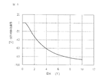
- FIG. 5 is a graph showing a change in capacitance according to a DC voltage applied to a smoothing capacitor whose equivalent circuit model is shown in FIG. 4 as a rate of change.
- FIG. 4 is a circuit diagram showing an equivalent circuit model of a choke coil constituting a power supply smoothing LC filter in the DC-DC converter shown in FIG. 3. It is a graph which shows the change (DC superposition characteristic) of the inductance in each load current of the choke coil by which an equivalent circuit model is shown in FIG. In this Embodiment, it is explanatory drawing used for description at the time of calculating
- the step-down DC-DC converter 1 is shown in a circuit diagram in FIG. 3, and includes a PWM switch block 2, an LC filter block 3, and a constant voltage control block 4.
- the PWM switch block 2 is provided with the input voltage V in to the input terminal 1a smoothed by the capacitor C in .
- the two MOSFETs (Moss structure field effect transistors) Q1 and Q2 are switched by the control circuit 5 so that the input voltage Vin is converted into a pulse train. Further, the duty cycle ratio of the output pulse train is changed by switching the MOSFETs Q1 and Q2, and the average value of the output pulse train is set to a desired output voltage.
- the LC filter block 3 includes a choke coil L and a smoothing capacitor Cout .
- the choke coil L and the smoothing capacitor Cout constitute a power supply smoothing LC filter, which attenuates the high-frequency component of the pulse train and smoothes the output voltage of the DC-DC converter 1 to a direct current.
- the output voltage V appearing at the output terminal 1b is divided by the resistor R1 and the resistor R2, and is compared with the reference voltage Vref by the error amplifier 6.
- An error signal between the output voltage V and the reference voltage V ref is amplified by the error amplifier 6 and output to the PWM comparator 7.
- the PWM comparator 7 compares the amplified error signal with a triangular wave or a sawtooth wave, and sends a control signal to the control circuit 5 so that the output voltage of the DC-DC converter 1 becomes a desired value.
- DC-DC converter 1 is limited by the input voltage V in, and outputs any of the DC current I and DC voltage V to the output terminal 1b in response to the control signal.
- FIG. 4 shows an equivalent circuit model of the smoothing capacitor Cout constituting the power supply smoothing LC filter.
- the equivalent circuit model of the smoothing capacitor C out is the main capacitive element C1 and the inductive element L2 and the resistor element R3 in series with the main resonance circuit 11 formed by connecting in series, resistor and capacitor elements C i capacitive circuit 12 formed by connecting the elements R i in parallel, the inductive element L i and the resistance element R i and a formed by connecting in parallel an inductive circuit 13, and the capacitor C i and the inductive element L i resistance
- a sub-resonant circuit 14 formed by connecting the element R i in parallel is connected.
- an insulation resistance IR is connected in parallel to the main capacitive element C1 of the main resonance circuit 11.
- a laminated ceramic chip capacitor 100 [microfarads] of 3216 size to the smoothing capacitor C out a laminated ceramic chip capacitor 100 [microfarads] of 3216 size to the smoothing capacitor C out.
- Table 1 below in which the values of the elements constituting the equivalent circuit model shown in Figure 4 the smoothing capacitor C out actually measured, and table data of the measured value.
- Table 2 is a table showing measured values obtained by changing the DC voltage applied to the smoothing capacitor C out [V] to the measured electrostatic capacitance [F] of a smoothing capacitor C out.
- FIG. 5 is a graph showing the change in capacitance according to the DC voltage applied to the smoothing capacitor C out as the rate of change from the actual measurement values shown in Table 2 above.
- the horizontal axis of the graph represents the applied DC voltage [V]
- the vertical axis represents the capacitance change rate [%].
- the capacitance change rate at which the smoothing capacitor Cout decreases increases gradually as the applied DC voltage increases.
- the capacitance change rate is expressed as the function k (V) shown in the following equation (1) using the applied DC voltage V as a variable: expressed.
- the capacitance change rate k (V) is expressed as a polynomial of the applied DC voltage V.
- k j is a constant
- the capacitance change rate k (V) in the graph shown in FIG. 5 is expressed by the following equation (2).
- the capacitance of the main capacitive element C1 of the main resonant circuit 11 constituting the equivalent circuit model of the smoothing capacitor Cout is expressed by the equation (2) corresponding to the DC output voltage of the DC-DC converter 1.
- the equivalent circuit model of the smoothing capacitor Cout is adapted to the DC output voltage V of the DC-DC converter 1 by multiplying the capacitance change rate k (V) to be corrected and correcting the capacitance of the main capacitive element C1.
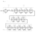
- FIG. 6 shows an equivalent circuit model of the choke coil L constituting the power supply smoothing LC filter in the DC-DC converter 1 shown in FIG.
- Equivalent circuit model of the choke coil L is configured to circuit comprising a resistance element R 4 in parallel circuit X 4 of the inductive element L 3 and the resistance element R 3 connected in series as a minimum unit.
- this minimum unit circuits circuit X 3 composed connected capacitive elements C 1 is in parallel to the series circuit of the circuit X 1 and the circuit X 2 are connected in series, it is constituted.
- Circuit X 1 is made to a series circuit of a resistance element R 1 and the capacitor C 2 is inductive element L 1 is connected in parallel circuit X 2 are connected to the resistance element R 2 and inductive element L 2 is in parallel Made up.
- Such impedance Z L of the choke coil L represented by the equivalent circuit model, assuming that the respective impedance of the circuit X 3 and circuit X 4 each X 3 and X 4, are represented by the following equation (3).
- each impedance X 3 and X 4 when the respective impedance of the circuit X 1 and circuit X 2 and X 1 and X 2, respectively, are expressed by the following equation (4) and (5).
- Each impedance X 1 and X 2 are represented by the following equation (6) and (7).
- the choke coil L is a 3030 size 4.7 [ ⁇ H] power inductor.
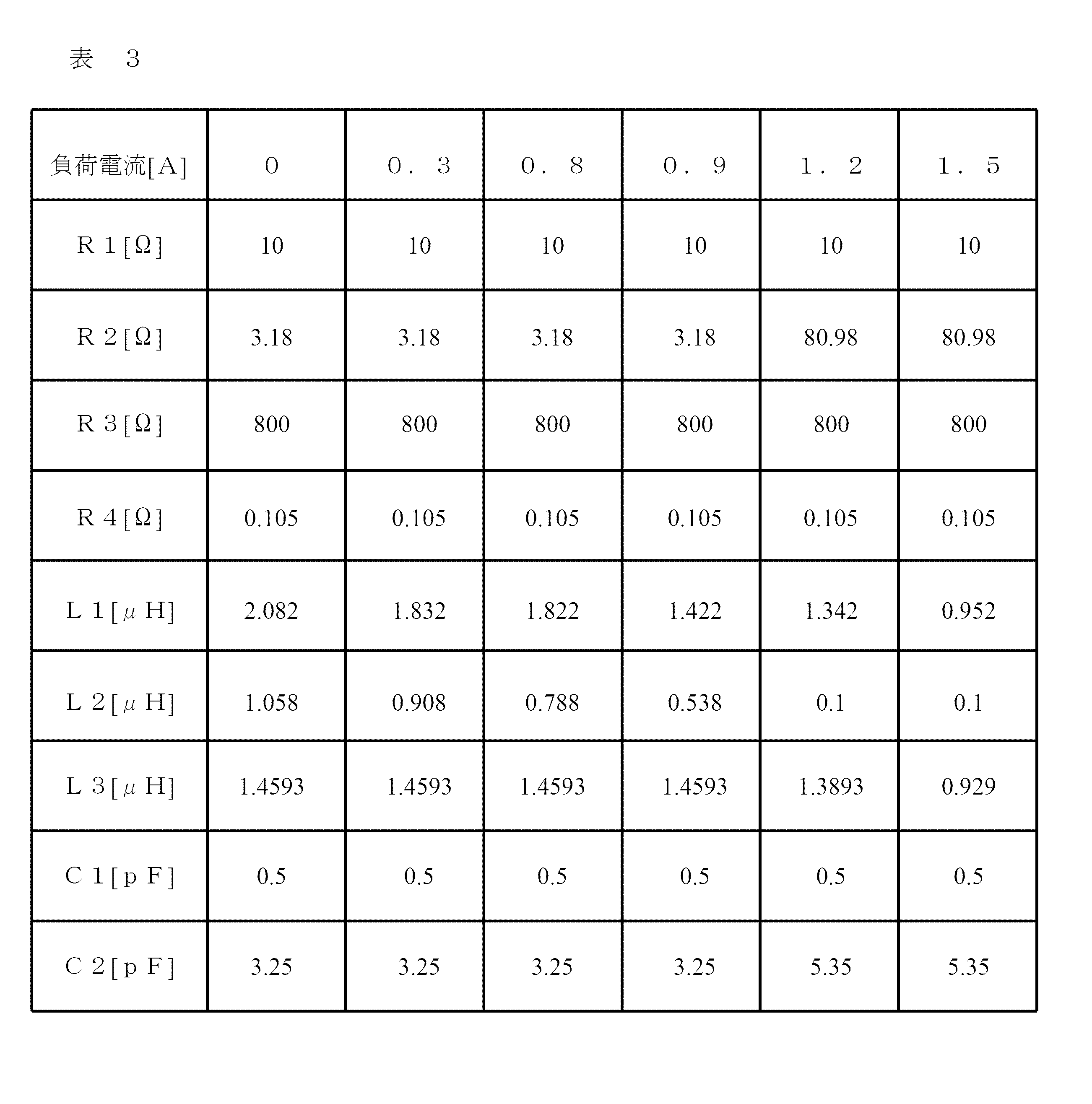
- Table 3 below shows the values of the elements constituting the equivalent circuit model of the choke coil L shown in FIG. 6 for a plurality of levels of the DC load current [A] flowing through the choke coil L, and the measured values are shown in Table 3 below. It is a table data.
- FIG. 7 is a graph showing the change (DC superposition characteristics) of the inductance [H] at each load current [A] of the choke coil L.
- the horizontal axis of the graph represents load current [A]
- the vertical axis represents inductance [H].
- the inductance of the choke coil L gradually decreases as the load current increases.
- Each inductance of the choke coil L at a plurality of levels of load current shown in Table 3 above can be obtained by applying the measured values shown in Table 3 to the equations (3) to (7). . Further, the inductance of the choke coil L at a load current other than the level shown in Table 3 is interpolated from the impedance of the choke coil L for a plurality of levels obtained based on the actually measured values shown in Table 3. Can be obtained.
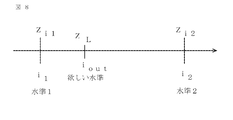
- the choke coil L at the desired level of load current i out is shown.
- the value of each element constituting the equivalent circuit model of the choke coil L is measured for a plurality of levels of direct current flowing through the choke coil L, and the impedance Z L of the choke coil L is determined.
- the impedance Z L of the choke coil L for the levels between the plurality of levels is obtained by interpolating from the impedance Z L of the choke coil L for the obtained levels.
- the equivalent circuit model of the choke coil L is a model corresponding to the level of the DC output current I of the DC-DC converter 1.
- the power supply smoothing LC filter in the DC-DC converter 1 generally has a transfer function G LC ( ⁇ ) expressed by the following equation (9).
- ⁇ angular frequency
- C out capacitance of smoothing capacitor C out
- L inductance of choke coil L
- ESR L real part of impedance of choke coil L
- RD S on-resistance of MOSFET Q1
- R d ON resistance of MOSFET Q2
- ESR C real part of impedance of smoothing capacitor C out
- R L output resistance.
- Re represents the real part of the impedance Z C.
- the equivalent circuit model of the power supply smoothing LC filter is derived by obtaining the transfer function G LC ( ⁇ ) expressed by the equation (9), as described above, the main capacitance of the main resonance circuit 11 is calculated.
- the capacitance C1 of the element C1 is multiplied by the capacitance change rate k (V) shown in the equation (2) corresponding to the DC output voltage V of the DC-DC converter 1 as shown in the equation (11).
- the electrostatic capacitance C1 of the main capacitive element C1 is corrected.
- the value according to the level of the load current of ESR L and L in the equation (9) representing the transfer function G LC ( ⁇ ) is the impedance Z L obtained in the equation (3) or (8 ) from the impedance Z L as determined by interpolating complete represented in formula, obtained by the following equation (13) and (14).
- Re represents the real part of the impedance Z L.
- the transfer function G LC ( ⁇ ) expressed by the equation (9) is obtained to derive the equivalent circuit model of the power supply smoothing LC filter
- the impedance Z L of the choke coil L is derived as described above.
- I is a value corresponding to the level of the DC load current I of the DC-DC converter 1.
- the transfer function G LC ( ⁇ ) represented by the equation (9) is transferred in accordance with the DC output voltage V and the DC output current I of the DC-DC converter 1 in this embodiment.
- the function G LC ( ⁇ , V, I) is obtained.
- FIG. 9 is a Bode diagram representing the transfer function G LC ( ⁇ , V, I) calculated as described above according to the present embodiment in comparison with the transfer function G LC ( ⁇ ) calculated using a one-element model. is there.
- this one-element model is composed of a one-element choke coil L and a one-element smoothing capacitor Cout .
- inductance 4.7 [.mu.H] choke coil L one element model was the electrostatic capacitance value of the smoothing capacitor C out and the conditions of 47 [ ⁇ F].
- the vertical axis of the Bode diagram is the absolute value [dB] of gain (Gain) and its phase (Phase) [°], and the horizontal axis is frequency ⁇ [Hz].
- the gain characteristic A1 according to the present embodiment is represented by a thick solid line, and the phase characteristic A2 is represented by a thick dotted line.
- the gain characteristic B1 by the one element model is represented by a thin solid line, and the phase characteristic B2 is represented by a thin dotted line.
- the gain characteristic A1 according to the present embodiment has a saturated gain attenuation at a high frequency
- the gain characteristic B1 based on the one-element model has a monotonically attenuated gain at a high frequency. is doing.
- phase characteristic A2 according to the present embodiment shows a tendency to return to 0 [°] at a high frequency
- phase characteristic B2 according to the one-element model is 180 [°] at a high frequency.
- the equivalent circuit model of the smoothing capacitor Cout is obtained by adding the DC output voltage of the DC-DC converter 1 to the electrostatic capacitance C1 of the main capacitive element C1 constituting the model.
- the capacitance change rate k (V) corresponding to V is multiplied as shown in the equation (11), and the capacitance C1 of the main capacitance element C1 is corrected, whereby the DC output of the DC-DC converter 1 is corrected.
- a model corresponding to the voltage V is used.
- the equivalent circuit model of the choke coil L is obtained by obtaining the impedance Z L of the choke coil L according to the equation (3) for a plurality of levels of the direct current I flowing through the choke coil L, and for the levels between the plurality of levels.
- the impedance Z L of the choke coil L is obtained by interpolating the impedance Z L of the choke coil L for the plurality of obtained levels using the equation (8), so that the DC output of the DC-DC converter 1 is obtained.
- the model corresponds to the level of the current I. Therefore, the equivalent circuit model of the power supply smoothing LC filter derived from the equivalent circuit models of the choke coil L and the smoothing capacitor is accurately derived according to the DC output voltage V and the DC output current I of the DC-DC converter 1.
- the characteristics of the power supply smoothing LC filter during the operation of the DC-DC converter 1 are accurately expressed. For this reason, the simulation in the circuit design of the DC-DC converter 1 is performed with high accuracy, and it is possible to contribute to the reduction in the number of trials and the shortening of the trial period in the circuit design of the DC-DC converter 1.
- the measured values of the elements constituting the equivalent circuit model of the smoothing capacitor Cout shown in FIG. 4 are converted into table data as shown in Table 1, and the choke coil L shown in FIG.
- the measured values of each element for a plurality of levels constituting the equivalent circuit model are converted into table data as shown in Table 3, so that the transfer function G LC ( ⁇ , V, I) is obtained and the power supply smoothing LC filter is obtained.
- the equivalent circuit model of the smoothing capacitor Cout is such that the capacitive circuit 12, the inductive circuit 13, and the sub-resonant circuit 14 are connected in series to the main resonant circuit 11, as shown in FIG.
- the capacitance change rate k (V) corresponding to the DC output voltage V of the DC-DC converter 1 is multiplied by the main capacitance element C1 constituting the main resonance circuit 11, and the main resonance circuit 11 is The electrostatic capacitance of the main capacitive element C1 is corrected. For this reason, the characteristic of the main resonance circuit 11 that most significantly represents the characteristic of the smoothing capacitor Cout is corrected, and the electrostatic capacitance of the smoothing capacitor Cout is most effective according to the DC output voltage V of the DC-DC converter 1. It is corrected to.
- the equivalent circuit model of the choke coil L as shown in FIG. 6, a resistance element R 4 connected in series with the parallel circuit X 4 of the inductive element L 3 and the resistance element R 3
- Various circuits are configured according to the accuracy and purpose of the simulation of the DC-DC converter 1 with the circuit as a minimum unit.
- the equivalent circuit model of the choke coil L of an equivalent circuit model and the plurality of levels of the smoothing capacitor C out, and the table data of in response to each type of the smoothing capacitor C out and the choke coil L may be configured as a library.
- the table data regarding the measured values of the elements constituting the equivalent circuit model of the smoothing capacitor C out and the measured values of the elements configuring the equivalent circuit model of the choke coil L are described.
- the table data (see Table 3) can be immediately extracted from the library according to each type of the smoothing capacitor C out and the choke coil L used in the DC-DC converter 1 to be simulated.
- the equivalent circuit models of the choke coil L and the smoothing capacitor C out during the operation of the DC-DC converter 1 correspond to the types of the smoothing capacitor C out and the choke coil L used in the DC-DC converter 1 to be simulated. Easily derived immediately.
- the equivalent circuit model of the smoothing capacitor Cout is illustrated as shown in FIG. 4, and the equivalent circuit model of the choke coil L is configured as shown in FIG.
- the shape of the circuit model is not limited to these.
- the equivalent circuit model of the smoothing capacitor Cout may be configured by connecting at least one of the capacitive circuit 12, the inductive circuit 13, and the sub-resonant circuit 14 to the main resonant circuit 11 in series. Good.
- the method for deriving the equivalent circuit model of the present embodiment described above can be easily used by using the following computer program.
- the computer program includes a first step for inputting the types of the smoothing capacitor Cout and the choke coil L, and a second step for inputting the values of the DC output voltage V and the DC output current I of the DC-DC converter 1.
- the equivalent circuit model (see FIG. 4) of the table data (see Table 1) prepared in advance for the type of smoothing capacitor Cout input in the first step is selected from the library, and the selected smoothing capacitor C
- the equivalent circuit model of the smoothing capacitor C out is determined according to the DC output voltage V input in the second step.
- the third step of making the model and the type of choke coil L input in the first step A prepared table data equivalent circuit model (see Table 3) (see FIG. 6) selected from the library Te, the impedance Z C of the choke coil L using the equivalent circuit model of the choke coil L selected
- a fifth step of deriving Le to function method of deriving the equivalent circuit model of the LC filter power supply smoothing of the present embodiment described above.
- the method for deriving the equivalent circuit model of the power supply smoothing LC filter of the present embodiment includes the types of the smoothing capacitor C out and the choke coil L constituting the DC-DC converter 1 to be simulated, and the DC output of the DC-DC converter 1.
- Each value of the voltage V and the DC output current I is input to the computer program, so that the computer program functions as described above.
- the equivalent circuit model of the smoothing capacitor C out is automatically set to a model corresponding to the input type smoothing capacitor C out and the input DC output voltage V by the computer program, and the choke coil L
- the equivalent circuit model is a model corresponding to the input type choke coil L and the DC output current I of the input value.
- the user of this derivation method determines the types of the smoothing capacitor Cout and the choke coil L constituting the DC-DC converter 1 to be simulated, and the DC output voltage V and the DC output current I of the DC-DC converter 1.
- an accurate simulation of the DC-DC converter 1 can be performed with high accuracy and ease.
- an accurate circuit simulation of the DC-DC converter 1 can be accurately and easily performed even by a general user who does not have specialized knowledge regarding circuit simulation.
- the computer program can be used from a terminal such as a personal computer connected to the Internet network by accessing a server such as an electronic component manufacturer having the computer program via the Internet network. According to this configuration, the user can easily use the computer program by accessing a server including the computer program from a terminal connected to the Internet network. Therefore, it is possible to provide a large number of users with a method for deriving an equivalent circuit model of the power supply smoothing LC filter according to the present embodiment.
Landscapes
- Engineering & Computer Science (AREA)
- Computer Hardware Design (AREA)
- Physics & Mathematics (AREA)
- Theoretical Computer Science (AREA)
- Evolutionary Computation (AREA)
- Geometry (AREA)
- General Engineering & Computer Science (AREA)
- General Physics & Mathematics (AREA)
- Power Engineering (AREA)
- Microelectronics & Electronic Packaging (AREA)
- Dc-Dc Converters (AREA)
Description
本発明は、直流安定化電源回路の出力電圧を安定化するチョークコイルと平滑コンデンサとから構成される電源平滑用LCフィルタの等価回路モデルを導出する導出方法に関するものである。
従来、この種の電源平滑用LCフィルタの等価回路モデルの導出方法としては、例えば、非特許文献1に開示されたスイッチング・レギュレータにおけるものがある。同文献では、降圧型コンバータをPWM(Pulse Width Modulation)スイッチブロック、LCフィルタブロックおよび定電圧制御部ブロックに分割し、分割したLCフィルタブロックの伝達関数XLCを求めている。そして、電源平滑用LCフィルタの入出力特性を、求めた伝達関数XLCによってシミュレーションすることで、電源平滑用LCフィルタの等価回路モデルを導出している。
また、電源平滑用LCフィルタの等価回路モデルは、LCフィルタを構成するインダクタおよびコンデンサの各等価回路モデルから導出することができる。
特許文献1では、周波数に依存しない抵抗(R)、キャパシタンス(C)、インダクタンス(L)を用いた、時間領域でのシミュレーションが可能な回路として、図1(a)に示すRC回路、および同図(b)に示すRL回路と、同図(c)に示すRCL回路のいずれかを、MLCC(Multi-Layer Ceramic Capacitor)の等価回路モデルとして、形成している。そして、形成した等価回路モデルの精度を判定するための評価関数を合成し、合成した評価関数を最小化することによって回路定数を決定している。
また、非特許文献2には、図2に示す、インダクタンスLとコアロス抵抗ACRとの並列回路に銅損抵抗DCRを直列に接続したモデルが、インダクタの等価回路モデルとして開示されている。そして、この等価回路モデルで表されるインダクタのどのファクターが電圧変換効率に影響するかが、同文献に記載されている。
馬場清太郎著「電源回路設計 成功のかぎ」、CQ出版、2009年8月1 日第2版、p253~p256
「1.電力変換効率に影響するインダクタのファクターの調査(降圧編)」、技術情報/テクニカルガイド/村田製作所、[online]、[平成24年6月12日検索]、インターネット<URL:http://www.murata.co.jp/products/power_inductor/tech_guide/tech_info.html>
近年、コスト削減を目的として、製品開発における試作回数の減少や、試作期間の短縮が実施されている。そのため、試作品の特性を事前にシミュレーションする重要性が以前より増してきており、試作回数の削減や試作期間の短縮のために、精度の良いシミュレーションの実施が不可欠になってきている。直流安定化電源回路設計におけるシミュレーションでは、電源平滑用LCフィルタの等価回路モデルを精度良く導出することが要請される。
しかしながら、直流安定化電源回路を構成するチョークコイルは電源回路の出力電流に、平滑コンデンサは電源回路の出力電圧に依存して特性が変化するので、上記従来の非特許文献1に開示された電源平滑用LCフィルタの等価回路モデルの導出方法では、電源回路の動作時における電源平滑用LCフィルタの特性を正確に表現するのは困難である。
また、特許文献1に開示されたコンデンサの等価回路モデルの導出方法では、コンデンサに重畳印加されるDCバイアス電圧の各値毎に等価回路モデルを導出する手間が必要となり、電源平滑用LCフィルタの等価回路モデルに適用した場合、電源回路の任意の出力電圧について等価回路モデルを導出することはできない。
また、非特許文献2に開示されたインダクタの等価回路モデルも、出力電流による重畳特性が加味されておらず、電源平滑用LCフィルタの等価回路モデルに適用した場合、電源回路の任意の出力電流について等価回路モデルを導出することはできない。
本発明はこのような課題を解決するためになされたもので、
直流安定化電源回路の出力電圧を安定化するチョークコイルと平滑コンデンサとから構成される電源平滑用LCフィルタの等価回路モデルをチョークコイルおよび平滑コンデンサの各等価回路モデルから導出する電源平滑用LCフィルタの等価回路モデルの導出方法において、
平滑コンデンサへの印加直流電圧に応じた平滑コンデンサの静電容量変化率を実測して印加直流電圧を変数とする関数として表し、平滑コンデンサの等価回路モデルを構成する容量素子の静電容量に直流安定化電源回路の直流出力電圧に応じた静電容量変化率を乗算して容量素子の静電容量を補正することで、平滑コンデンサの等価回路モデルを直流安定化電源回路の直流出力電圧に応じたモデルとし、
チョークコイルの等価回路モデルを構成する各要素の値をチョークコイルを流れる直流電流の複数の水準について実測してチョークコイルのインピーダンスを複数の水準について求めておき、複数の水準の間の水準についてのチョークコイルのインピーダンスは、求めておいた複数の水準についてのチョークコイルのインピーダンスから内挿補完して求めることで、チョークコイルの等価回路モデルを直流安定化電源回路の直流出力電流の水準に応じたモデルとする
ことを特徴とする。
直流安定化電源回路の出力電圧を安定化するチョークコイルと平滑コンデンサとから構成される電源平滑用LCフィルタの等価回路モデルをチョークコイルおよび平滑コンデンサの各等価回路モデルから導出する電源平滑用LCフィルタの等価回路モデルの導出方法において、
平滑コンデンサへの印加直流電圧に応じた平滑コンデンサの静電容量変化率を実測して印加直流電圧を変数とする関数として表し、平滑コンデンサの等価回路モデルを構成する容量素子の静電容量に直流安定化電源回路の直流出力電圧に応じた静電容量変化率を乗算して容量素子の静電容量を補正することで、平滑コンデンサの等価回路モデルを直流安定化電源回路の直流出力電圧に応じたモデルとし、
チョークコイルの等価回路モデルを構成する各要素の値をチョークコイルを流れる直流電流の複数の水準について実測してチョークコイルのインピーダンスを複数の水準について求めておき、複数の水準の間の水準についてのチョークコイルのインピーダンスは、求めておいた複数の水準についてのチョークコイルのインピーダンスから内挿補完して求めることで、チョークコイルの等価回路モデルを直流安定化電源回路の直流出力電流の水準に応じたモデルとする
ことを特徴とする。
本構成によれば、平滑コンデンサの等価回路モデルは、そのモデルを構成する容量素子の静電容量に直流安定化電源回路の直流出力電圧に応じた静電容量変化率が乗算されて、容量素子の静電容量が補正されることで、直流安定化電源回路の直流出力電圧に応じたモデルとされる。チョークコイルの等価回路モデルは、チョークコイルを流れる直流電流の複数の水準についてチョークコイルのインピーダンスを求めておき、複数の水準の間の水準についてのチョークコイルのインピーダンスは、求めておいた複数の水準についてのチョークコイルのインピーダンスから内挿補完して求めることで、直流安定化電源回路の直流出力電流の水準に応じたモデルとされる。従って、チョークコイルおよび平滑コンデンサの各等価回路モデルから導出される電源平滑用LCフィルタの等価回路モデルは、直流安定化電源回路の直流出力電圧および直流出力電流に応じて精度良く導出され、直流安定化電源回路の動作時における電源平滑用LCフィルタの特性は正確に表現される。このため、直流安定化電源回路設計におけるシミュレーションが精度良く実施されて、直流安定化電源回路設計における試作回数の削減や試作期間の短縮に資することが可能となる。
また、本発明は、
平滑コンデンサの等価回路モデルを構成する各要素の測定値をテーブルデータ化しておき、電源平滑用LCフィルタの等価回路モデルを導出する際にテーブルデータ化しておいた平滑コンデンサの等価回路モデルを使って平滑コンデンサの等価回路モデルを直流安定化電源回路の直流出力電圧に応じたモデルとし、
チョークコイルの等価回路モデルを構成する各要素の測定値を複数の水準についてテーブルデータ化しておき、電源平滑用LCフィルタの等価回路モデルを導出する際にテーブルデータ化しておいたチョークコイルの各等価回路モデルを使ってチョークコイルの等価回路モデルを直流安定化電源回路の直流出力電流に応じたモデルとする
ことを特徴とする。
平滑コンデンサの等価回路モデルを構成する各要素の測定値をテーブルデータ化しておき、電源平滑用LCフィルタの等価回路モデルを導出する際にテーブルデータ化しておいた平滑コンデンサの等価回路モデルを使って平滑コンデンサの等価回路モデルを直流安定化電源回路の直流出力電圧に応じたモデルとし、
チョークコイルの等価回路モデルを構成する各要素の測定値を複数の水準についてテーブルデータ化しておき、電源平滑用LCフィルタの等価回路モデルを導出する際にテーブルデータ化しておいたチョークコイルの各等価回路モデルを使ってチョークコイルの等価回路モデルを直流安定化電源回路の直流出力電流に応じたモデルとする
ことを特徴とする。
本構成によれば、平滑コンデンサの等価回路モデルを構成する各要素の測定値、およびチョークコイルの等価回路モデルを構成する複数の水準についての各要素の測定値をテーブルデータ化しておくことで、電源平滑用LCフィルタの等価回路モデルを導出する際に、容易に、直流安定化電源回路の直流出力電圧に応じた平滑コンデンサの等価回路モデルおよび直流安定化電源回路の直流出力電流に応じたチョークコイルの等価回路モデルを導出することができる。このため、直流安定化電源回路の動作時におけるチョークコイルおよび平滑コンデンサの各等価回路モデルを簡単に再現して用いることができるようになる。
また、本発明は、平滑コンデンサの等価回路モデルおよび複数の水準についてのチョークコイルの等価回路モデルを平滑コンデンサおよびチョークコイルの各種類に応じてテーブルデータ化してライブラリー化しておくことを特徴とする。
本構成によれば、平滑コンデンサの等価回路モデルを構成する各要素の測定値についてのテーブルデータ、およびチョークコイルの等価回路モデルを構成する各要素の測定値についてのテーブルデータは、シミュレートする直流安定化電源回路に用いる平滑コンデンサおよびチョークコイルの各種類に応じて、ライブラリから直ちに引き出すことができる。このため、直流安定化電源回路の動作時におけるチョークコイルおよび平滑コンデンサの各等価回路モデルは、シミュレートする直流安定化電源回路に用いる平滑コンデンサおよびチョークコイルの各種類に応じて、容易に直ちに導出される。
また、本発明は、平滑コンデンサの等価回路モデルが、容量素子と抵抗素子とを並列に接続して成る容量性回路、誘導素子と抵抗素子とを並列に接続して成る誘導性回路、および容量素子と誘導素子と抵抗素子とを並列に接続して成る副共振回路のうちの少なくとも1つが、主容量素子と誘導素子と抵抗素子とを直列に接続して成る主共振回路に直列に接続されて構成され、
静電容量の補正が主共振回路を構成する主容量素子に対して行われることを特徴とする。
静電容量の補正が主共振回路を構成する主容量素子に対して行われることを特徴とする。
本構成によれば、平滑コンデンサの等価回路モデルは、容量性回路、誘導性回路、および副共振回路のうちの少なくとも1つが主共振回路に直列に接続されて構成され、直流安定化電源回路の直流出力電圧に応じた静電容量変化率は主共振回路を構成する主容量素子に対して乗算されて、主共振回路を構成する主容量素子の静電容量が補正される。このため、平滑コンデンサの特性を最も顕著に表す主共振回路の特性が補正されて、平滑コンデンサの静電容量は直流安定化電源回路の直流出力電圧に応じて最も効果的に補正される。
また、本発明は、チョークコイルの等価回路モデルが、誘導素子と抵抗素子との並列回路に抵抗素子を直列に接続して成る回路を最小単位として構成されることを特徴とする。
本構成によれば、チョークコイルの等価回路モデルは、誘導素子と抵抗素子との並列回路に抵抗素子を直列に接続して成る回路を最小単位として、直流安定化電源回路のシミュレーションの精度や目的に応じて多様に構成される。
また、本発明は、
平滑コンデンサおよびチョークコイルの種類を入力する第1のステップと、直流安定化電源回路の直流出力電圧および直流出力電流の各値を入力する第2のステップと、第1のステップで入力された種類の平滑コンデンサについて予め用意されたテーブルデータの等価回路モデルをライブラリーの中から選択し、選択した平滑コンデンサの等価回路モデルを使って平滑コンデンサの等価回路モデルを第2のステップで入力された直流出力電圧に応じたモデルとする第3のステップと、第1のステップで入力された種類のチョークコイルについて予め用意されたテーブルデータの等価回路モデルをライブラリーの中から選択し、選択したチョークコイルの等価回路モデルを使ってチョークコイルの等価回路モデルを第2のステップで入力された直流出力電流に応じたモデルとする第4のステップと、第3のステップで導出した平滑コンデンサの等価回路モデルおよび第4のステップで導出したチョークコイルの等価回路モデルを使って第2のステップで入力された直流出力電圧および直流出力電流に応じた電源平滑用LCフィルタの等価回路モデルを導出する第5のステップとを備え、電源平滑用LCフィルタの等価回路モデルの導出方法を機能させるコンピュータプログラムを構成した。
平滑コンデンサおよびチョークコイルの種類を入力する第1のステップと、直流安定化電源回路の直流出力電圧および直流出力電流の各値を入力する第2のステップと、第1のステップで入力された種類の平滑コンデンサについて予め用意されたテーブルデータの等価回路モデルをライブラリーの中から選択し、選択した平滑コンデンサの等価回路モデルを使って平滑コンデンサの等価回路モデルを第2のステップで入力された直流出力電圧に応じたモデルとする第3のステップと、第1のステップで入力された種類のチョークコイルについて予め用意されたテーブルデータの等価回路モデルをライブラリーの中から選択し、選択したチョークコイルの等価回路モデルを使ってチョークコイルの等価回路モデルを第2のステップで入力された直流出力電流に応じたモデルとする第4のステップと、第3のステップで導出した平滑コンデンサの等価回路モデルおよび第4のステップで導出したチョークコイルの等価回路モデルを使って第2のステップで入力された直流出力電圧および直流出力電流に応じた電源平滑用LCフィルタの等価回路モデルを導出する第5のステップとを備え、電源平滑用LCフィルタの等価回路モデルの導出方法を機能させるコンピュータプログラムを構成した。
本構成によれば、シミュレートする直流安定化電源回路を構成する平滑コンデンサおよびチョークコイルの種類、並びに直流安定化電源回路の直流出力電圧および直流出力電流の各値がコンピュータプログラムに入力されることで、上記の電源平滑用LCフィルタの等価回路モデルの導出方法がコンピュータプログラムによって機能させられる。つまり、コンピュータプログラムにより、自動的に、平滑コンデンサの等価回路モデルは入力された種類の平滑コンデンサおよび入力された値の直流出力電圧に応じたモデルとされ、また、チョークコイルの等価回路モデルは入力された種類のチョークコイルおよび入力された値の直流出力電流に応じたモデルとされる。このため、本導出方法の利用者は、シミュレートする直流安定化電源回路を構成する平滑コンデンサおよびチョークコイルの種類、並びに直流安定化電源回路の直流出力電圧および直流出力電流の各値をコンピュータプログラムに入力するだけで、直流安定化電源回路の的確なシミュレーションを高精度かつ簡単に行える。この結果、回路シミュレートに関する専門知識を持たない一般の利用者であっても、直流安定化電源回路の的確な回路シミュレーションを高精度かつ簡単に行える。
また、本発明は、前記コンピュータプログラムを備えるサーバにインターネット網を介してアクセスし、インターネット網に接続された端末から前記コンピュータプログラムを使用するコンピュータプログラムの使用方法を構成した。
本構成によれば、利用者は、インターネット網に接続された端末から前記コンピュータプログラムを備えるサーバにアクセスすることで、前記コンピュータプログラムを容易に使用することが出来る。このため、本発明による電源平滑用LCフィルタの等価回路モデルの導出方法を多数の利用者に提供することが可能になる。
本発明によれば、上記のように、直流安定化電源回路の動作時における電源平滑用LCフィルタの特性は正確に表現される。このため、直流安定化電源回路設計におけるシミュレーションが精度良く実施されて、直流安定化電源回路設計における試作回数の削減や試作期間の短縮に資することが可能となる。
次に、本発明の一実施の形態による電源平滑用LCフィルタの等価回路モデルの導出方法を、降圧型DC-DCコンバータにおける電源平滑用LCフィルタに適用した場合について、説明する。
降圧型DC-DCコンバータ1は、図3に回路図が示され、PWMスイッチブロック2、LCフィルタブロック3および定電圧制御部ブロック4から構成されている。
PWMスイッチブロック2には、入力端子1aへの入力電圧VinがコンデンサCinで平滑されたものが与えられる。PWMスイッチブロック2では、2個のMOSFET(モス構造電界効果トランジスタ)Q1,Q2が制御回路5によってスイッチングされることで、入力電圧Vinがパルス列に変換される。また、MOSFETQ1,Q2のスイッチングにより、出力パルス列のデューティーサイクル比が変えられ、出力パルス列の平均値は所望の出力電圧にされる。LCフィルタブロック3は、チョークコイルLと平滑コンデンサCoutとから構成されている。チョークコイルLと平滑コンデンサCoutとは電源平滑用LCフィルタを構成し、パルス列の高周波成分を減衰させて、DC-DCコンバータ1の出力電圧を直流に平滑化する。
定電圧制御部ブロック4では、出力端子1bに現れる出力電圧Vが抵抗R1と抵抗R2とによって分圧されて、エラーアンプ6において基準電圧Vrefと比較される。出力電圧Vと基準電圧Vrefとの誤差信号はエラーアンプ6によって増幅されて、PWMコンパレータ7へ出力される。PWMコンパレータ7は、増幅された誤差信号を三角波あるいはのこぎり波と比較して、DC-DCコンバータ1の出力電圧が所望の値になるように、制御回路5に制御信号を送る。DC-DCコンバータ1は、入力電圧Vinの制限を受けるが、この制御信号に応じて任意の直流電流Iおよび直流電圧Vを出力端子1bへ出力する。
図4は、上記の電源平滑用LCフィルタを構成する平滑コンデンサCoutの等価回路モデルを示す。
本実施の形態では、平滑コンデンサCoutの等価回路モデルは、主容量素子C1と誘導素子L2と抵抗素子R3とを直列に接続して成る主共振回路11に直列に、容量素子Ciと抵抗素子Riとを並列に接続して成る容量性回路12、誘導素子Liと抵抗素子Riとを並列に接続して成る誘導性回路13、および容量素子Ciと誘導素子Liと抵抗素子Riとを並列に接続して成る副共振回路14が接続されて、構成されている。ここで、各素子の添え字iはノード番号を示し、これら各回路12~14ではi=4~15に設定されている。また、各回路12~14は容量素子Ciと誘導素子Liと抵抗素子Riとの並列回路として表されており、容量性回路における誘導素子Li=0、誘導性回路における容量素子Ci=0である。また、主共振回路11の主容量素子C1には絶縁抵抗IRが並列に接続されて表現されている。
本実施の形態では、平滑コンデンサCoutに3216サイズの100[μF]の積層セラミック・チップ・コンデンサを用いた。下記の表1は、この平滑コンデンサCoutの図4に示す等価回路モデルを構成する各要素の値を実測し、その測定値をテーブルデータ化したものである。
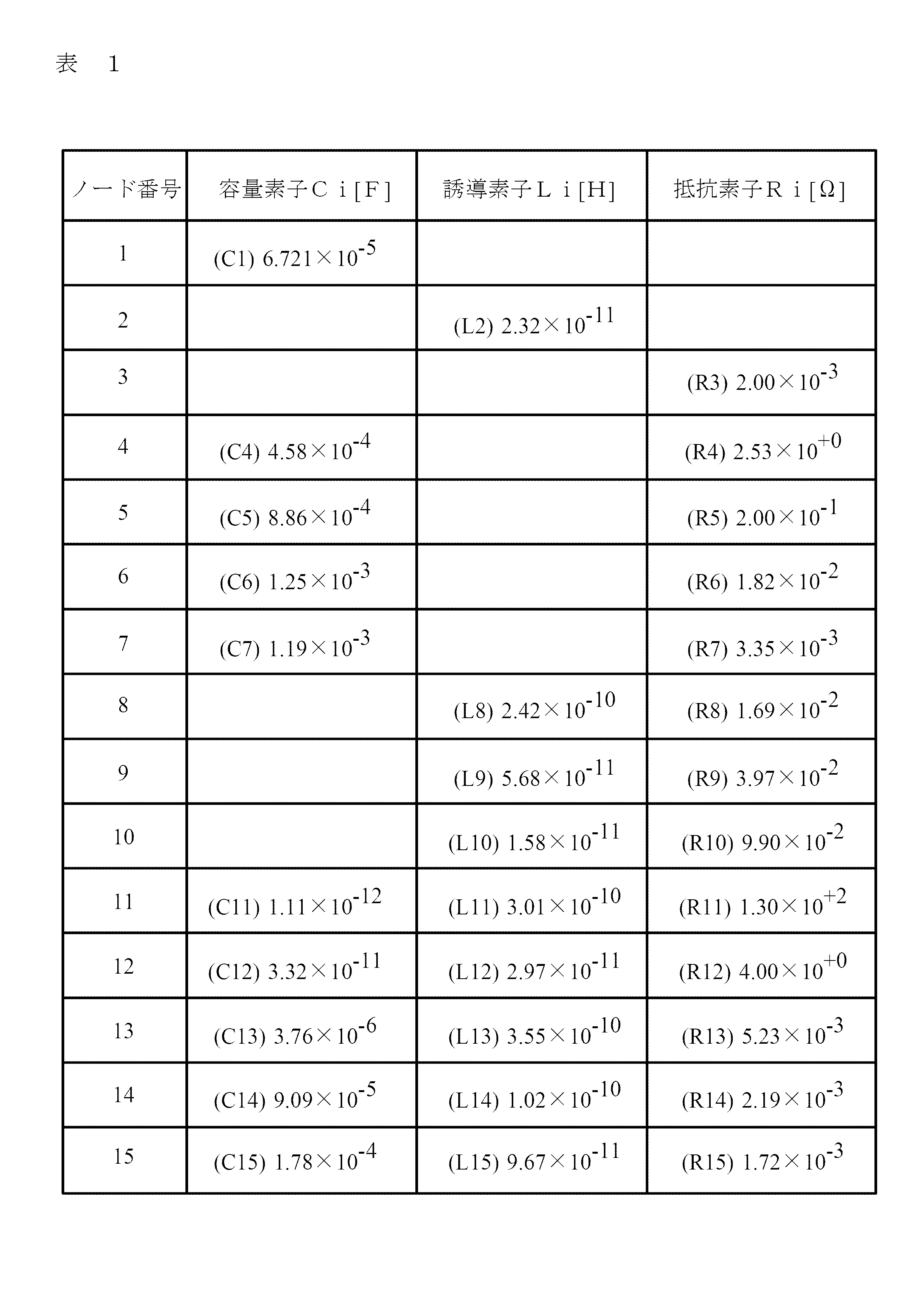
ここで、空欄は、素子値=0で、対応する素子が存在しないことを表している。また、下記の表2は、平滑コンデンサCoutへ印加する直流電圧[V]を変化させて平滑コンデンサCoutの静電容量[F]を実測して得られた実測値を示すテーブルである。
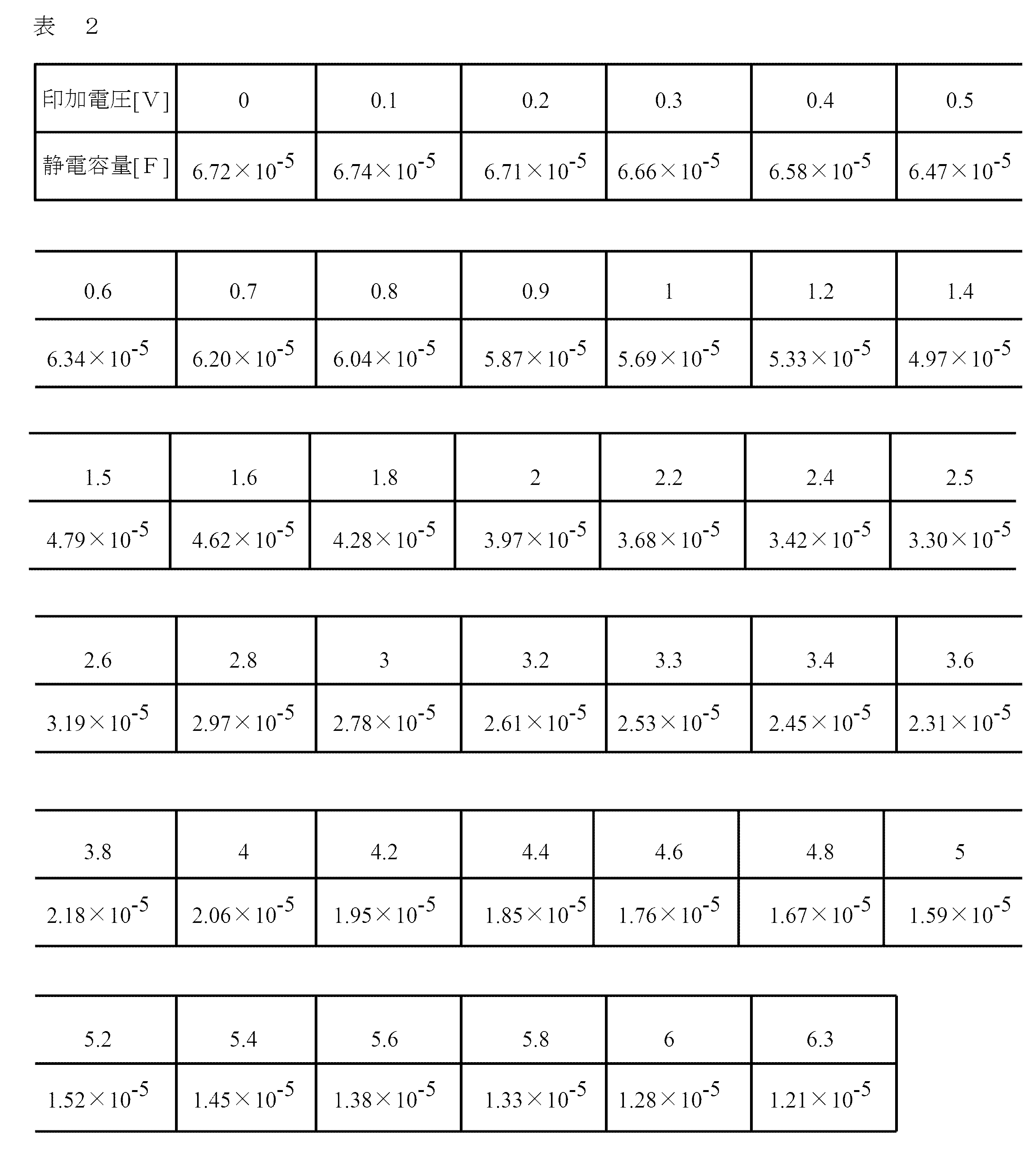
また、図5は、上記の表2に示される実測値から、平滑コンデンサCoutへの印加直流電圧に応じた静電容量の変化を変化率として表したグラフである。同グラフの横軸は印加直流電圧[V]、縦軸は静電容量変化率[%]を表す。同グラフに示されるように、平滑コンデンサCoutの減少する静電容量変化率は、印加直流電圧の増加に応じて漸次増加する。この静電容量変化率は、本実施の形態のように平滑コンデンサCoutがセラミックコンデンサの場合は、印加直流電圧Vを変数とする次の(1)式に示される関数k(V)として、表される。

(1)式に示されるように、静電容量変化率k(V)は印加直流電圧Vの多項式として表される。ここで、kjは定数であり、図5に示すグラフにおける静電容量変化率k(V)は次の(2)式に表される。

本実施の形態では、平滑コンデンサCoutの等価回路モデルを構成する主共振回路11の主容量素子C1の静電容量に、DC-DCコンバータ1の直流出力電圧に応じた式(2)に示される静電容量変化率k(V)を乗算して、主容量素子C1の静電容量を補正することで、平滑コンデンサCoutの等価回路モデルをDC-DCコンバータ1の直流出力電圧Vに応じたモデルとする。
図6は、図3に示すDC-DCコンバータ1において上記の電源平滑用LCフィルタを構成するチョークコイルLの等価回路モデルを示す。
チョークコイルLの等価回路モデルは、誘導素子L3と抵抗素子R3との並列回路X4に抵抗素子R4を直列に接続して成る回路を最小単位として構成される。本実施の形態では、この最小単位回路に、回路X1と回路X2との直列回路に容量素子C1が並列に接続されて成る回路X3が直列に接続されて、構成されている。回路X1は、抵抗素子R1と容量素子C2との直列回路に誘導素子L1が並列に接続されて成り、回路X2は、抵抗素子R2と誘導素子L2とが並列に接続されて成る。
このような等価回路モデルで表されるチョークコイルLのインピーダンスZLは、回路X3および回路X4の各インピーダンスをそれぞれX3およびX4とすると、次の(3)式によって表される。

ここで、各インピーダンスX3およびX4は、回路X1および回路X2の各インピーダンスをそれぞれX1およびX2とすると、次の(4)式および(5)式によって表される。

また、各インピーダンスX1およびX2は、次の(6)式および(7)式によって表される。

本実施の形態では、チョークコイルLに3030サイズの4.7[μH]のパワーインダクタを用いた。下記の表3は、このチョークコイルLの図6に示す等価回路モデルを構成する各要素の値を、チョークコイルLに流れる直流負荷電流[A]の複数の水準について実測し、その測定値をテーブルデータ化したものである。
また、図7は、チョークコイルLの各負荷電流[A]におけるインダクタンス[H]の変化(直流重畳特性)を示すグラフである。同グラフの横軸は負荷電流[A]、縦軸はインダクタンス[H]を表す。同グラフに示されるように、チョークコイルLのインダクタンスは、負荷電流の増加に応じて漸次小さくなる。
上記の表3に示される複数の水準の負荷電流におけるチョークコイルLの各インダクタンスは、表3に示される実測値を(3)~(7)式に適用することで、求めておくことが出来る。また、表3に示される水準以外の負荷電流におけるチョークコイルLのインダクタンスは、表3に示される実測値に基づいて求めておいた複数の水準についてのチョークコイルLのインピーダンスから、内挿補完して求めことが出来る。
例えば、図8に示すように、欲しい水準の負荷電流ioutが水準1の負荷電流i1と水準2の負荷電流i2との間に有る場合、欲しい水準の負荷電流ioutにおけるチョークコイルLのインピーダンスZLは、負荷電流i1におけるインピーダンスZi1と負荷電流i2におけるインピーダンスZi2とから、次の(8)式に示される内挿補完よって求められる。

本実施の形態では、上記のように、チョークコイルLの等価回路モデルを構成する各要素の値をチョークコイルLを流れる直流電流の複数の水準について実測して、チョークコイルLのインピーダンスZLを複数の水準について求めておき、複数の水準の間の水準についてのチョークコイルLのインピーダンスZLは、求めておいた複数の水準についてのチョークコイルLのインピーダンスZLから内挿補完して求めることで、チョークコイルLの等価回路モデルをDC-DCコンバータ1の直流出力電流Iの水準に応じたモデルとする。
DC-DCコンバータ1における電源平滑用LCフィルタは、一般的にその伝達関数GLC(ω)が次の(9)式に表される。

ここで、ω:角周波数、Cout:平滑コンデンサCoutの静電容量、L:チョークコイルLのインダクタンス、ESRL:チョークコイルLのインピーダンスの実部、RDS:MOSFETQ1のオン抵抗、Rd:MOSFETQ2のオン抵抗、ESRC:平滑コンデンサCoutのインピーダンスの実部、RL:出力抵抗である。
平滑コンデンサCoutの印加直流電圧Vに応じたインピーダンスZC(V)は、平滑コンデンサCoutの等価回路モデルを構成する主共振回路11の主容量素子C1の静電容量をC1とすると、次の(10)式に表される。

従って、伝達関数GLC(ω)を表す(9)式におけるCoutおよびESRCの印加直流電圧Vに応じた値Cout(V)およびESRC(V)は、上記の(10)式に表されるインピーダンスZC(V)から、次の(11)式および(12)式によって求められる。

ここで、ReはインピーダンスZCの実部を表す。本実施の形態では、(9)式に表される伝達関数GLC(ω)を求めて電源平滑用LCフィルタの等価回路モデルを導出する際、上記のように、主共振回路11の主容量素子C1の静電容量C1に、DC-DCコンバータ1の直流出力電圧Vに応じた式(2)に示される静電容量変化率k(V)を(11)式に示すように乗算して、主容量素子C1の静電容量C1を補正する。
また、伝達関数GLC(ω)を表す(9)式におけるESRLおよびLの負荷電流の水準に応じた値は、(3)式に表される求めておいたインピーダンスZL、または(8)式に表される内挿補完によって求められるインピーダンスZLから、次の(13)式および(14)式によって求められる。

ここで、ReはインピーダンスZLの実部を表す。本実施の形態では、(9)式に表される伝達関数GLC(ω)を求めて電源平滑用LCフィルタの等価回路モデルを導出する際、上記のように、チョークコイルLのインピーダンスZLをDC-DCコンバータ1の直流負荷電流Iの水準に応じた値とする。この結果、一般的に(9)式に表される伝達関数GLC(ω)は、本実施の形態では、DC-DCコンバータ1の直流出力電圧Vおよび直流出力電流Iに応じた値の伝達関数GLC(ω,V,I)となる。
図9は、本実施の形態によって上記のように計算した伝達関数GLC(ω,V,I)を、一素子モデルによって計算した伝達関数GLC(ω)と比較して表すボーデ線図である。
この一素子モデルは、図3の回路図におけるLCフィルタブロック3に表されるように、一素子のチョークコイルLと一素子の平滑コンデンサCoutとから構成される。また、この計算では、一素子モデルのチョークコイルLのインダクタンスを4.7[μH]、平滑コンデンサCoutの静電容量値を47[μF]の条件とした。また、DC-DCコンバータ1の直流出力電圧Vを1.8[V]、直流出力電流Iを1.5[A]、スイッチング周波数を400[kHz]とし、MOSFETQ1のオン抵抗RDSを27[mΩ]、MOSFETQ2のオン抵抗Rdを21[mΩ]、負荷抵抗RLを100[Ω]とした。
ボーデ線図の縦軸はゲイン(Gain)の絶対値[dB]とその位相(Phase)[°]であり、横軸は周波数ω[Hz]である。また、本実施の形態によるゲイン特性A1は太い実線で表し、位相特性A2は太い点線で表している。一素子モデルによるゲイン特性B1は細い実線で表し、位相特性B2は細い点線で表している。同図に示されるように、本実施の形態によるゲイン特性A1は、高い周波数においてゲインの減衰が飽和しているのに対し、一素子モデルによるゲイン特性B1は、高い周波数においてゲインが単調に減衰している。また、本実施の形態による位相特性A2は、高い周波数において0[°]に戻る傾向を示しているのに対し、一素子モデルによる位相特性B2は、高い周波数において180[°]になっている。このことから、本実施の形態によるシミュレーションでは、チョークコイルLおよび平滑コンデンサCoutの動特性が加味され、実回路に近い振る舞いが得られたことが分かる。
このような本実施の形態によれば、上記のように、平滑コンデンサCoutの等価回路モデルは、そのモデルを構成する主容量素子C1の静電容量C1にDC-DCコンバータ1の直流出力電圧Vに応じた静電容量変化率k(V)が(11)式に示すように乗算されて、主容量素子C1の静電容量C1が補正されることで、DC-DCコンバータ1の直流出力電圧Vに応じたモデルとされる。また、チョークコイルLの等価回路モデルは、チョークコイルLを流れる直流電流Iの複数の水準についてチョークコイルLのインピーダンスZLを(3)式に従って求めておき、複数の水準の間の水準についてのチョークコイルLのインピーダンスZLは、求めておいた複数の水準についてのチョークコイルLのインピーダンスZLから(8)式を用いて内挿補完して求めることで、DC-DCコンバータ1の直流出力電流Iの水準に応じたモデルとされる。従って、チョークコイルLおよび平滑コンデンサの各等価回路モデルから導出される電源平滑用LCフィルタの等価回路モデルは、DC-DCコンバータ1の直流出力電圧Vおよび直流出力電流Iに応じて精度良く導出され、DC-DCコンバータ1の動作時における電源平滑用LCフィルタの特性は正確に表現される。このため、DC-DCコンバータ1の回路設計におけるシミュレーションが精度良く実施されて、DC-DCコンバータ1の回路設計における試作回数の削減や試作期間の短縮に資することが可能となる。
また、本実施の形態では、図4に示す平滑コンデンサCoutの等価回路モデルを構成する各要素の測定値を表1に示すようにテーブルデータ化しておくと共に、図6に示すチョークコイルLの等価回路モデルを構成する複数の水準についての各要素の測定値を表3に示すようにテーブルデータ化しておくことで、伝達関数GLC(ω,V,I)を求めて電源平滑用LCフィルタの等価回路モデルを導出する際に、容易に、平滑コンデンサCoutのインピーダンスZCおよびチョークコイルLのインピーダンスZLの計算が出来て、容易に、DC-DCコンバータ1の直流出力電圧Vに応じた平滑コンデンサCoutの等価回路モデルおよびDC-DCコンバータ1の直流出力電流Iに応じたチョークコイルLの等価回路モデルを導出することができる。このため、DC-DCコンバータ1の動作時におけるチョークコイルLおよび平滑コンデンサCoutの各等価回路モデルを簡単に再現して用いることができるようになる。
また、本実施の形態では、平滑コンデンサCoutの等価回路モデルが、図4に示すように、容量性回路12、誘導性回路13、および副共振回路14が主共振回路11に直列に接続されて構成され、DC-DCコンバータ1の直流出力電圧Vに応じた静電容量変化率k(V)は主共振回路11を構成する主容量素子C1に対して乗算されて、主共振回路11を構成する主容量素子C1の静電容量が補正される。このため、平滑コンデンサCoutの特性を最も顕著に表す主共振回路11の特性が補正されて、平滑コンデンサCoutの静電容量はDC-DCコンバータ1の直流出力電圧Vに応じて最も効果的に補正される。
また、本実施の形態では、チョークコイルLの等価回路モデルは、図6に示すように、誘導素子L3と抵抗素子R3との並列回路X4に抵抗素子R4を直列に接続して成る回路を最小単位として、DC-DCコンバータ1のシミュレーションの精度や目的に応じて多様に構成される。
なお、上記の実施の形態において、平滑コンデンサCoutの等価回路モデルおよび複数の水準についてのチョークコイルLの等価回路モデルを、平滑コンデンサCoutおよびチョークコイルLの各種類に応じてテーブルデータ化して、ライブラリー化しておくように構成してもよい。
本構成によれば、平滑コンデンサCoutの等価回路モデルを構成する各要素の測定値についてのテーブルデータ(表1参照)、およびチョークコイルLの等価回路モデルを構成する各要素の測定値についてのテーブルデータ(表3参照)は、シミュレートするDC-DCコンバータ1に用いる平滑コンデンサCoutおよびチョークコイルLの各種類に応じて、ライブラリから直ちに引き出すことができる。このため、DC-DCコンバータ1の動作時におけるチョークコイルLおよび平滑コンデンサCoutの各等価回路モデルは、シミュレートするDC-DCコンバータ1に用いる平滑コンデンサCoutおよびチョークコイルLの各種類に応じて、容易に直ちに導出される。
また、上記の実施の形態においては、平滑コンデンサCoutの等価回路モデルを図4に示すように、チョークコイルLの等価回路モデルを図6に示すように構成した場合について説明したが、各等価回路モデルの形はこれらに限定されることは無い。例えば、平滑コンデンサCoutの等価回路モデルは、容量性回路12、誘導性回路13、および副共振回路14のうちの少なくとも1つを主共振回路11に直列に接続して構成するようにしてもよい。
上述した本実施の形態の等価回路モデルの導出方法は、次のコンピュータプログラムを用いることで、簡単に利用することが出来る。このコンピュータプログラムは、平滑コンデンサCoutおよびチョークコイルLの種類を入力する第1のステップと、DC-DCコンバータ1の直流出力電圧Vおよび直流出力電流Iの各値を入力する第2のステップと、第1のステップで入力された種類の平滑コンデンサCoutについて予め用意されたテーブルデータ(表1参照)の等価回路モデル(図4参照)をライブラリーの中から選択し、選択した平滑コンデンサCoutの等価回路モデルを使って平滑コンデンサCoutのインピーダンスZCを(10)式によって計算することで、平滑コンデンサCoutの等価回路モデルを第2のステップで入力された直流出力電圧Vに応じたモデルとする第3のステップと、第1のステップで入力された種類のチョークコイルLについて予め用意されたテーブルデータ(表3参照)の等価回路モデル(図6参照)をライブラリーの中から選択し、選択したチョークコイルLの等価回路モデルを使ってチョークコイルLのインピーダンスZCを(3)式および(8)式によって計算することで、チョークコイルLの等価回路モデルを第2のステップで入力された直流出力電流Iに応じたモデルとする第4のステップと、第3のステップで導出した平滑コンデンサCoutの等価回路モデルおよび第4のステップで導出したチョークコイルLの等価回路モデルを使って電源平滑用LCフィルタの伝達関数GLC(ω,V,I)を(9)式によって求めることで、第2のステップで入力された直流出力電圧Vおよび直流出力電流Iに応じた電源平滑用LCフィルタの等価回路モデルを導出する第5のステップとを備え、上述した本実施の形態の電源平滑用LCフィルタの等価回路モデルの導出方法を機能させる。
本実施の形態の電源平滑用LCフィルタの等価回路モデルの導出方法は、シミュレートするDC-DCコンバータ1を構成する平滑コンデンサCoutおよびチョークコイルLの種類、並びにDC-DCコンバータ1の直流出力電圧Vおよび直流出力電流Iの各値がコンピュータプログラムに入力されることで、上記のようにコンピュータプログラムによって機能させられる。つまり、コンピュータプログラムにより、自動的に、平滑コンデンサCoutの等価回路モデルは入力された種類の平滑コンデンサCoutおよび入力された値の直流出力電圧Vに応じたモデルとされ、また、チョークコイルLの等価回路モデルは入力された種類のチョークコイルLおよび入力された値の直流出力電流Iに応じたモデルとされる。このため、本導出方法の利用者は、シミュレートするDC-DCコンバータ1を構成する平滑コンデンサCoutおよびチョークコイルLの種類、並びにDC-DCコンバータ1の直流出力電圧Vおよび直流出力電流Iの各値をコンピュータプログラムに入力するだけで、DC-DCコンバータ1の的確なシミュレーションを高精度かつ簡単に行える。この結果、回路シミュレートに関する専門知識を持たない一般の利用者であっても、DC-DCコンバータ1の的確な回路シミュレーションを高精度かつ簡単に行える。
また、上記のコンピュータプログラムは、上記コンピュータプログラムを備える電子部品製造メーカなどのサーバにインターネット網を介してアクセスすることで、インターネット網に接続されたパーソナルコンピュータ等の端末から使用することが出来る。本構成によれば、利用者は、インターネット網に接続された端末から上記コンピュータプログラムを備えるサーバにアクセスすることで、上記コンピュータプログラムを容易に使用することが出来る。このため、本実施の形態による電源平滑用LCフィルタの等価回路モデルの導出方法を多数の利用者に提供することが可能になる。
1…降圧型DC-DCコンバータ
2…PWMスイッチブロック
3…LCフィルタブロック
4…定電圧制御部ブロック
5…制御回路
6…エラーアンプ
7…PWMコンパレータ
11…主共振回路
12…容量性回路
13…誘導性回路
14…副共振回路
Cout…平滑コンデンサ
L…チョークコイル
C1…主容量素子
2…PWMスイッチブロック
3…LCフィルタブロック
4…定電圧制御部ブロック
5…制御回路
6…エラーアンプ
7…PWMコンパレータ
11…主共振回路
12…容量性回路
13…誘導性回路
14…副共振回路
Cout…平滑コンデンサ
L…チョークコイル
C1…主容量素子
Claims (7)
- 直流安定化電源回路の出力電圧を安定化するチョークコイルと平滑コンデンサとから構成される電源平滑用LCフィルタの等価回路モデルを前記チョークコイルおよび前記平滑コンデンサの各等価回路モデルから導出する電源平滑用LCフィルタの等価回路モデルの導出方法において、
前記平滑コンデンサへの印加直流電圧に応じた前記平滑コンデンサの静電容量変化率を実測して前記印加直流電圧を変数とする関数として表し、前記平滑コンデンサの等価回路モデルを構成する容量素子の静電容量に前記直流安定化電源回路の直流出力電圧に応じた前記静電容量変化率を乗算して前記容量素子の静電容量を補正することで、前記平滑コンデンサの等価回路モデルを前記直流安定化電源回路の直流出力電圧に応じたモデルとし、
前記チョークコイルの等価回路モデルを構成する各要素の値を前記チョークコイルを流れる直流電流の複数の水準について実測して前記チョークコイルのインピーダンスを前記複数の水準について求めておき、前記複数の水準の間の水準についての前記チョークコイルのインピーダンスは、求めておいた前記複数の水準についての前記チョークコイルのインピーダンスから内挿補完して求めることで、前記チョークコイルの等価回路モデルを前記直流安定化電源回路の直流出力電流の水準に応じたモデルとする
ことを特徴とする電源平滑用LCフィルタの等価回路モデルの導出方法。 - 前記平滑コンデンサの等価回路モデルを構成する各要素の測定値をテーブルデータ化しておき、電源平滑用LCフィルタの等価回路モデルを導出する際にテーブルデータ化しておいた前記平滑コンデンサの等価回路モデルを使って前記平滑コンデンサの等価回路モデルを前記直流安定化電源回路の直流出力電圧に応じたモデルとし、
前記チョークコイルの等価回路モデルを構成する各要素の測定値を前記複数の水準についてテーブルデータ化しておき、電源平滑用LCフィルタの等価回路モデルを導出する際にテーブルデータ化しておいた前記チョークコイルの各等価回路モデルを使って前記チョークコイルの等価回路モデルを前記直流安定化電源回路の直流出力電流に応じたモデルとする
ことを特徴とする請求項1に記載の電源平滑用LCフィルタの等価回路モデルの導出方法。 - 前記平滑コンデンサの等価回路モデルおよび前記複数の水準についての前記チョークコイルの等価回路モデルを前記平滑コンデンサおよび前記チョークコイルの各種類に応じてテーブルデータ化してライブラリー化しておくことを特徴とする請求項2に記載の電源平滑用LCフィルタの等価回路モデルの導出方法。
- 前記平滑コンデンサの等価回路モデルは、容量素子と抵抗素子とを並列に接続して成る容量性回路、誘導素子と抵抗素子とを並列に接続して成る誘導性回路、および容量素子と誘導素子と抵抗素子とを並列に接続して成る副共振回路のうちの少なくとも1つが、主容量素子と誘導素子と抵抗素子とを直列に接続して成る主共振回路に直列に接続されて構成され、
静電容量の前記補正は前記主共振回路を構成する前記主容量素子に対して行われる
ことを特徴とする請求項1から請求項3のいずれか1項に記載の電源平滑用LCフィルタの等価回路モデルの導出方法。 - 前記チョークコイルの等価回路モデルは、誘導素子と抵抗素子との並列回路に抵抗素子を直列に接続して成る回路を最小単位として構成されることを特徴とする請求項1から請求項4のいずれか1項に記載の電源平滑用LCフィルタの等価回路モデルの導出方法。
- 前記平滑コンデンサおよび前記チョークコイルの種類を入力する第1のステップと、前記直流安定化電源回路の直流出力電圧および直流出力電流の各値を入力する第2のステップと、前記第1のステップで入力された種類の前記平滑コンデンサについて予め用意されたテーブルデータの等価回路モデルをライブラリーの中から選択し、選択した前記平滑コンデンサの等価回路モデルを使って前記平滑コンデンサの等価回路モデルを前記第2のステップで入力された直流出力電圧に応じたモデルとする第3のステップと、前記第1のステップで入力された種類の前記チョークコイルについて予め用意されたテーブルデータの等価回路モデルをライブラリーの中から選択し、選択した前記チョークコイルの等価回路モデルを使って前記チョークコイルの等価回路モデルを前記第2のステップで入力された直流出力電流に応じたモデルとする第4のステップと、前記第3のステップで導出した前記平滑コンデンサの等価回路モデルおよび前記第4のステップで導出した前記チョークコイルの等価回路モデルを使って前記第2のステップで入力された直流出力電圧および直流出力電流に応じた電源平滑用LCフィルタの等価回路モデルを導出する第5のステップとを備え、請求項3に記載の電源平滑用LCフィルタの等価回路モデルの導出方法を機能させるコンピュータプログラム。
- 前記コンピュータプログラムを備えるサーバにインターネット網を介してアクセスし、インターネット網に接続された端末から前記コンピュータプログラムを使用する請求項6に記載のコンピュータプログラムの使用方法。
Priority Applications (1)
| Application Number | Priority Date | Filing Date | Title |
|---|---|---|---|
| JP2014529420A JP5943080B2 (ja) | 2012-08-07 | 2013-07-25 | 電源平滑用lcフィルタの等価回路モデルの導出方法 |
Applications Claiming Priority (2)
| Application Number | Priority Date | Filing Date | Title |
|---|---|---|---|
| JP2012175189 | 2012-08-07 | ||
| JP2012-175189 | 2012-08-07 |
Publications (1)
| Publication Number | Publication Date |
|---|---|
| WO2014024692A1 true WO2014024692A1 (ja) | 2014-02-13 |
Family
ID=50067925
Family Applications (1)
| Application Number | Title | Priority Date | Filing Date |
|---|---|---|---|
| PCT/JP2013/070190 Ceased WO2014024692A1 (ja) | 2012-08-07 | 2013-07-25 | 電源平滑用lcフィルタの等価回路モデルの導出方法 |
Country Status (2)
| Country | Link |
|---|---|
| JP (1) | JP5943080B2 (ja) |
| WO (1) | WO2014024692A1 (ja) |
Cited By (3)
| Publication number | Priority date | Publication date | Assignee | Title |
|---|---|---|---|---|
| WO2015015910A1 (ja) * | 2013-07-29 | 2015-02-05 | 株式会社村田製作所 | 印加交流電圧を考慮したコンデンサの静電容量値決定方法およびプログラム |
| KR20160000165A (ko) * | 2014-06-24 | 2016-01-04 | 삼성전기주식회사 | 복합 전자부품 및 그 실장 기판 |
| JP2024114995A (ja) * | 2023-02-14 | 2024-08-26 | 三菱電機株式会社 | 電磁波計算システムおよびバックデータの取得方法 |
Family Cites Families (2)
| Publication number | Priority date | Publication date | Assignee | Title |
|---|---|---|---|---|
| JP2004318416A (ja) * | 2003-04-15 | 2004-11-11 | Toshiba Tec Corp | 回路設計支援サーバ、回路設計支援方法及び回路設計支援プログラム |
| JP2010033369A (ja) * | 2008-07-29 | 2010-02-12 | Fujitsu Ltd | 解析装置および解析方法 |
-
2013
- 2013-07-25 WO PCT/JP2013/070190 patent/WO2014024692A1/ja not_active Ceased
- 2013-07-25 JP JP2014529420A patent/JP5943080B2/ja active Active
Non-Patent Citations (3)
| Title |
|---|
| GIJUTSU JOHO: "Denryoku Henkan Koritsu ni Eikyo suru Inductor no Factor no Chosa (Koatsu Hen)", TECHNICAL GUIDE, 28 June 2010 (2010-06-28), Retrieved from the Internet <URL:http://web.archive.org/web/20100628044739> [retrieved on 20130930] * |
| HIDEAKI DEGUCHI ET AL.: "Measurement for current dependency of coil inductance using a transient current switching circuit", IEICE TECHNICAL REPORT, vol. 106, no. 361, 10 November 2006 (2006-11-10), pages 13 - 16 * |
| PRYMAK, JOHN D.: "SPICE Modeling of Capacitors", CARTS, 1995, pages 1 - 5, Retrieved from the Internet <URL:http://www.kemet.com/kemet/web/homepage/kfbk3.nsf/vaFeedbackFAQ/BF2C1E6AF9D9BB3085257225006B3082/$file/1995%20CARTS%20-%20SPICE.pdf> [retrieved on 20130930] * |
Cited By (6)
| Publication number | Priority date | Publication date | Assignee | Title |
|---|---|---|---|---|
| WO2015015910A1 (ja) * | 2013-07-29 | 2015-02-05 | 株式会社村田製作所 | 印加交流電圧を考慮したコンデンサの静電容量値決定方法およびプログラム |
| JP5999266B2 (ja) * | 2013-07-29 | 2016-09-28 | 株式会社村田製作所 | 印加交流電圧を考慮したコンデンサの静電容量値決定方法およびプログラム |
| US10184967B2 (en) | 2013-07-29 | 2019-01-22 | Murata Manufacturing Co., Ltd. | Method of determining capacitance value of capacitor while taking applied alternating voltage into consideration, and program |
| KR20160000165A (ko) * | 2014-06-24 | 2016-01-04 | 삼성전기주식회사 | 복합 전자부품 및 그 실장 기판 |
| KR102004794B1 (ko) * | 2014-06-24 | 2019-07-29 | 삼성전기주식회사 | 복합 전자부품 및 그 실장 기판 |
| JP2024114995A (ja) * | 2023-02-14 | 2024-08-26 | 三菱電機株式会社 | 電磁波計算システムおよびバックデータの取得方法 |
Also Published As
| Publication number | Publication date |
|---|---|
| JP5943080B2 (ja) | 2016-06-29 |
| JPWO2014024692A1 (ja) | 2016-07-25 |
Similar Documents
| Publication | Publication Date | Title |
|---|---|---|
| CN102326130B (zh) | 确定来自滤波器组件信息的操作特性的开关电源(smps)控制器集成电路 | |
| US10521533B2 (en) | Inductor simulation method and inductor nonlinear equivalent circuit model | |
| JP5861774B2 (ja) | コンデンサの等価回路モデルの導出方法 | |
| US9563728B2 (en) | Equivalent circuit model, program, and recording medium | |
| Zhang | Modeling and loop compensation design of switching mode power supplies | |
| US10650180B2 (en) | Capacitor simulation method and capacitor nonlinear equivalent circuit model | |
| CN109962638A (zh) | 电力转换装置 | |
| Siddhartha et al. | Systematic circuit design and analysis of a non‐ideal DC–DC pulse width modulation boost converter | |
| US10789399B2 (en) | Compensation design of power converters | |
| CN110518801A (zh) | 一种双重移相调制下双有源全桥变换器小信号建模方法 | |
| CN120528225B (zh) | 多路输出ac-dc开关电源的电压纹波抑制及补偿方法 | |
| JP5943080B2 (ja) | 電源平滑用lcフィルタの等価回路モデルの導出方法 | |
| CN110249517B (zh) | 电源装置及电源装置的控制方法 | |
| Erickson et al. | Converter transfer functions | |
| Huang et al. | A novel describing function small-signal modeling approach for passive ripple constant on-time controlled converter with exponentially varying slope | |
| Wang et al. | Stability prediction of integrated-circuit based constant ON-time controlled buck converters | |
| Subasinghage et al. | Stability analysis and experimental validation of the supercapacitor‐assisted low‐dropout regulator | |
| Li et al. | Analysis of parameter effects on the small-signal dynamics of Buck converters with average current mode control | |
| Tishechkin et al. | Adaptive capacitance impedance matching (ACIM) of WPT systems by voltage controlled capacitors | |
| Yao | Modeling and design of a current mode control boost converter | |
| CN110543703B (zh) | 一种考虑不同时间尺度的准谐振变换器建模分析方法 | |
| CN116317456B (zh) | 一种分数阶电感构造的控制方法及控制结构 | |
| CN119078555B (zh) | 一种电动汽车的充电效率优化方法、装置及电动汽车 | |
| Shetty | A quick and simplified approach for understanding the dynamics of the SEPIC converter for low voltage applications: Simulation study | |
| CN119226808A (zh) | 电感匹配方法、装置、通信设备及存储介质 |
Legal Events
| Date | Code | Title | Description |
|---|---|---|---|
| 121 | Ep: the epo has been informed by wipo that ep was designated in this application |
Ref document number: 13827927 Country of ref document: EP Kind code of ref document: A1 |
|
| ENP | Entry into the national phase |
Ref document number: 2014529420 Country of ref document: JP Kind code of ref document: A |
|
| NENP | Non-entry into the national phase |
Ref country code: DE |
|
| 122 | Ep: pct application non-entry in european phase |
Ref document number: 13827927 Country of ref document: EP Kind code of ref document: A1 |