WO2014020988A1 - 有機薄膜太陽電池及びその製造方法 - Google Patents
有機薄膜太陽電池及びその製造方法 Download PDFInfo
- Publication number
- WO2014020988A1 WO2014020988A1 PCT/JP2013/065580 JP2013065580W WO2014020988A1 WO 2014020988 A1 WO2014020988 A1 WO 2014020988A1 JP 2013065580 W JP2013065580 W JP 2013065580W WO 2014020988 A1 WO2014020988 A1 WO 2014020988A1
- Authority
- WO
- WIPO (PCT)
- Prior art keywords
- layer
- bulk heterojunction
- organic semiconductor
- type organic
- solar cell
- Prior art date
- Legal status (The legal status is an assumption and is not a legal conclusion. Google has not performed a legal analysis and makes no representation as to the accuracy of the status listed.)
- Ceased
Links
Images

Classifications
-
- H—ELECTRICITY
- H10—SEMICONDUCTOR DEVICES; ELECTRIC SOLID-STATE DEVICES NOT OTHERWISE PROVIDED FOR
- H10K—ORGANIC ELECTRIC SOLID-STATE DEVICES
- H10K30/00—Organic devices sensitive to infrared radiation, light, electromagnetic radiation of shorter wavelength or corpuscular radiation
- H10K30/30—Organic devices sensitive to infrared radiation, light, electromagnetic radiation of shorter wavelength or corpuscular radiation comprising bulk heterojunctions, e.g. interpenetrating networks of donor and acceptor material domains
-
- H—ELECTRICITY
- H10—SEMICONDUCTOR DEVICES; ELECTRIC SOLID-STATE DEVICES NOT OTHERWISE PROVIDED FOR
- H10K—ORGANIC ELECTRIC SOLID-STATE DEVICES
- H10K30/00—Organic devices sensitive to infrared radiation, light, electromagnetic radiation of shorter wavelength or corpuscular radiation
- H10K30/50—Photovoltaic [PV] devices
-
- H—ELECTRICITY
- H10—SEMICONDUCTOR DEVICES; ELECTRIC SOLID-STATE DEVICES NOT OTHERWISE PROVIDED FOR
- H10K—ORGANIC ELECTRIC SOLID-STATE DEVICES
- H10K85/00—Organic materials used in the body or electrodes of devices covered by this subclass
- H10K85/10—Organic polymers or oligomers
- H10K85/111—Organic polymers or oligomers comprising aromatic, heteroaromatic, or aryl chains, e.g. polyaniline, polyphenylene or polyphenylene vinylene
-
- H—ELECTRICITY
- H10—SEMICONDUCTOR DEVICES; ELECTRIC SOLID-STATE DEVICES NOT OTHERWISE PROVIDED FOR
- H10K—ORGANIC ELECTRIC SOLID-STATE DEVICES
- H10K85/00—Organic materials used in the body or electrodes of devices covered by this subclass
- H10K85/10—Organic polymers or oligomers
- H10K85/111—Organic polymers or oligomers comprising aromatic, heteroaromatic, or aryl chains, e.g. polyaniline, polyphenylene or polyphenylene vinylene
- H10K85/113—Heteroaromatic compounds comprising sulfur or selene, e.g. polythiophene
-
- H—ELECTRICITY
- H10—SEMICONDUCTOR DEVICES; ELECTRIC SOLID-STATE DEVICES NOT OTHERWISE PROVIDED FOR
- H10K—ORGANIC ELECTRIC SOLID-STATE DEVICES
- H10K85/00—Organic materials used in the body or electrodes of devices covered by this subclass
- H10K85/40—Organosilicon compounds, e.g. TIPS pentacene
-
- Y—GENERAL TAGGING OF NEW TECHNOLOGICAL DEVELOPMENTS; GENERAL TAGGING OF CROSS-SECTIONAL TECHNOLOGIES SPANNING OVER SEVERAL SECTIONS OF THE IPC; TECHNICAL SUBJECTS COVERED BY FORMER USPC CROSS-REFERENCE ART COLLECTIONS [XRACs] AND DIGESTS
- Y02—TECHNOLOGIES OR APPLICATIONS FOR MITIGATION OR ADAPTATION AGAINST CLIMATE CHANGE
- Y02E—REDUCTION OF GREENHOUSE GAS [GHG] EMISSIONS, RELATED TO ENERGY GENERATION, TRANSMISSION OR DISTRIBUTION
- Y02E10/00—Energy generation through renewable energy sources
- Y02E10/50—Photovoltaic [PV] energy
- Y02E10/549—Organic PV cells
-
- Y—GENERAL TAGGING OF NEW TECHNOLOGICAL DEVELOPMENTS; GENERAL TAGGING OF CROSS-SECTIONAL TECHNOLOGIES SPANNING OVER SEVERAL SECTIONS OF THE IPC; TECHNICAL SUBJECTS COVERED BY FORMER USPC CROSS-REFERENCE ART COLLECTIONS [XRACs] AND DIGESTS
- Y02—TECHNOLOGIES OR APPLICATIONS FOR MITIGATION OR ADAPTATION AGAINST CLIMATE CHANGE
- Y02P—CLIMATE CHANGE MITIGATION TECHNOLOGIES IN THE PRODUCTION OR PROCESSING OF GOODS
- Y02P70/00—Climate change mitigation technologies in the production process for final industrial or consumer products
- Y02P70/50—Manufacturing or production processes characterised by the final manufactured product
Definitions
- the present invention relates to an organic thin film solar cell including a bulk heterojunction layer and a method for manufacturing the same.
- a bulk heterojunction type organic thin film solar cell in which a bulk heterojunction layer is formed between a transparent electrode layer and a counter electrode layer as one of thin film solar cells using an organic material (hereinafter referred to as an organic thin film solar cell). (See Non-Patent Document 1).
- a bulk heterojunction type organic thin film solar cell is formed by applying a coating liquid containing a p-type organic semiconductor, an n-type organic semiconductor, and an organic solvent on one electrode layer. It is manufactured by forming a bulk heterojunction layer.
- the first requirement is related to the domain size.
- the bulk heterojunction layer absorbs light, excitons are generated in the domain, and the excitons diffuse into the domain and reach the pn interface, and then are separated into free charges.
- the exciton diffusion length in the bulk heterojunction layer is small and is 10 to 20 nm.
- the domain size is larger than this diffusion length, free charges are not generated because excitons are deactivated before reaching the pn interface. Therefore, it is ideal that the domain size is 10 nm or less.
- the second requirement is related to the connection structure between domains.
- the domains In the bulk heterojunction layer, it is considered that holes conduct through a domain of a p-type material and electrons conduct through a domain of an n-type material. Therefore, in a situation where the domains are separated from each other, even if free charge is generated, it cannot be conducted to the electrode. Under these circumstances, it is ideal that the domains are in contact with each other to form a percolation structure.
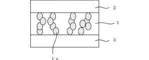
- the structure of the bulk heterojunction layer 1 is that the domain 1a has a size smaller than the diffusion length of excitons and the domain 1a is an electrode as shown in FIG. What has the percolation structure connected to a few is ideal.
- an object of the present invention is to provide an organic thin-film solar cell with excellent power generation performance by optimizing the structure of the bulk heterojunction layer. Moreover, it is providing the manufacturing method for it.
- the present inventors have shown that the structure that has been considered to be ideal as the structure of the bulk heterojunction layer shown in FIG. 4 is not necessarily preferable for solar cell performance, and the short circuit current is reduced. Found that it is likely to bring
- the organic thin-film solar cell of the present invention includes a bulk heterojunction layer in which a domain of a p-type organic semiconductor and a domain of an n-type organic semiconductor are phase-separated, and either directly on the one side of the bulk heterojunction layer
- An organic thin-film solar cell comprising an anode disposed via a layer and a cathode disposed directly or via another layer on the other side of the bulk heterojunction layer,
- domains of a p-type organic semiconductor having an average diameter of 1 nm or more and 30 nm or less are dispersed, and a percolation structure in which the domains of the p-type organic semiconductor are connected to connect both electrodes is formed. It is characterized by not.
- the domain of the p-type organic semiconductor has a substantially spherical shape and is dispersed in the bulk heterojunction layer.
- the p-type organic semiconductor is an amorphous material and the n-type semiconductor is a fullerene derivative.
- a hole blocking layer is preferably inserted between the bulk heterojunction layer and the cathode.
- the manufacturing method of the organic thin-film solar cell of the present invention includes a step of forming a first electrode layer on a substrate, and a p-type organic semiconductor on the first electrode layer directly or via another layer. a step of applying a coating solution containing an n-type organic semiconductor and an organic solvent to form a coating film; a step of forming a second electrode layer on the coating film directly or via another layer; A step of heat-treating the coating film at 50 ° C. or more and 140 ° C. or less for 10 minutes or more and 30 minutes or less after forming the second electrode layer.
- the short-circuit current, the open-circuit voltage, and the fill factor are improved, and high energy conversion efficiency can be realized.
- the coating liquid containing a p-type organic semiconductor, an n-type organic semiconductor, and an organic solvent on the 1st electrode layer directly or through another layer After forming a coating film, a second electrode layer is formed on the coating film directly or via another layer, and then the coating film is formed at 50 ° C. or more and 140 ° C. or less for 10 minutes or more and 30 minutes.
- the domain of the p-type organic semiconductor having an average diameter of 1 nm or more and 30 nm or less is dispersed, and the domain of the p-type organic semiconductor is connected to form a percolation structure that connects the electrodes.
- An organic thin film solar cell having a bulk heterojunction layer that is not formed can be manufactured.
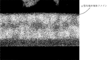
- FIG. 4 is a cross-sectional projection view of a bulk heterojunction layer of Test Example 1.
- FIG. 6 is a cross-sectional projection view of a bulk heterojunction layer of Test Example 2.
- FIG. It is the schematic of the bulk heterojunction layer considered conventionally ideal.
- the organic thin film solar cell shown in FIG. 1 is formed by sequentially laminating a first electrode layer 12, a bulk heterojunction layer 13, and a second electrode layer 14 on a substrate 11.
- the substrate 11 is not particularly limited.
- an insulating plastic film substrate such as a polyimide film, a polyethylene terephthalate film, a polyethylene naphthalate film, a polyethersulfone film, an acrylic film, an aramid film, a glass substrate, a stainless steel substrate, or the like can be used.
- substrate is distribute
- FIG. Examples of the electrode material of the electrode layer disposed on the light incident side include transparent conductive oxides such as ITO (indium oxide + tin oxide), ZnO, TiO 2 , SnO 2 , and IZO (indium oxide + zinc oxide).
- Examples of the electrode material of the electrode layer disposed on the non-light-receiving side include metals such as Al, Mg, Ca, and alloys thereof.
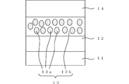
- the bulk heterojunction layer 13 has a structure in which a domain 13a of a p-type organic semiconductor and a domain 13b of an n-type organic semiconductor are phase-separated.
- the p-type organic semiconductor domains 13a having an average diameter of 1 nm to 30 nm are dispersed almost uniformly in the bulk heterojunction layer 13, and the p-type organic semiconductor domains 13a The percolation structure by 13a is not formed.
- an organic thin-film solar cell capable of realizing high energy conversion efficiency with improved short-circuit current, open-circuit voltage, and fill factor. Can do. The reason for this is not known in detail, but is probably because some of the holes generated at the pn interface are conducted to the n-type organic semiconductor domain in addition to the p-type organic semiconductor domain. It is assumed.
- the domain size of the domain 13a of the p-type organic semiconductor is an average diameter of 1 nm or more and 30 nm or less.
- the average diameter is more preferably 1 nm or more and 20 nm or less, and particularly preferably 1 nm or more and 10 nm or less. If the domain size exceeds 30 nm, excitons are deactivated before reaching the pn interface, and free charges are hardly generated. Further, if the domain size is too small, the number of absorbed photons per unit film thickness tends to decrease and the short circuit current tends to decrease, so the lower limit is 1 nm.
- the shape of the domain 13a of the p-type organic semiconductor is preferably substantially spherical. If it is substantially spherical, the internal electric field generated in the film thickness direction efficiently acts on the pn interface, and the charge separation efficiency is increased.
- phase separation structure of the bulk heterojunction layer 13 is prepared by using Scanning Transmission Electron Microscope (STEM), Electron Energy Loss SpectroEL, Spectral Spectroscopy, etc. This can be confirmed by observing the image.
- STEM Scanning Transmission Electron Microscope
- Electron Energy Loss SpectroEL Electron Energy Loss SpectroEL
- Spectral Spectroscopy etc. This can be confirmed by observing the image.
- any organic material having an electron donating property can be used.
- compounds such as thiophene, phenylene vinylene, thienylene vinylene, carbazole, vinyl carbazole, pyrrole, isothiaphene and heptadiene, and the above compounds having a hydroxyl group, an alkyl group, an amino group, a methyl group, a nitro group, a halogen group, etc.
- Examples include, but are not limited to, polymers of derivatives. These may be used alone or in combination of two or more.
- compounds of the following formulas (1) to (14) can be mentioned as an example.
- n is preferably 5 to 150, more preferably 10 to 100.
- the compounds represented by the formulas (1) and (6) are crystalline compounds. Further, the compounds represented by the formulas (7) to (14) are amorphous (non-crystalline).
- the p-type organic semiconductor may be crystalline or amorphous (amorphous). Since the crystalline organic semiconductor material has high domain elasticity, the domain 13a of the p-type organic semiconductor as shown in FIG. 1 is dispersed almost uniformly in the bulk heterojunction layer 13, and the domain of the p-type organic semiconductor is obtained. It is easy to adopt the bulk heterojunction layer 13 having a structure in which the percolation structure by 13a is not formed. Therefore, a crystalline material is particularly preferably used for the p-type organic semiconductor. The degree of stereoregularity of the p-type organic semiconductor is not questioned.
- the weight average molecular weight of the p-type organic semiconductor depends on the material used and cannot be generally mentioned, but is preferably 2,000 to 150,000.
- any organic material having an electron accepting property can be used.
- examples thereof include fullerene derivatives and perylene derivatives.
- fullerene derivatives are particularly preferable because electron transfer from the p-type organic semiconductor is particularly fast.
- Preferred examples of the fullerene derivative include a fullerene C 60 derivative, a fullerene C 70 derivative, and a fullerene C 80 derivative.
- PCBM Phenyl-C 61 -Butyric-Acid -Methyl Ester
- bis-PCBM Bisadduct-Phenyl-C 61 -Butyric- Acid-Methyl Ester
- the first electrode layer 12 and the second electrode layer 14 are directly formed on both sides of the bulk heterojunction layer 13.
- a hole blocking layer may be formed between the electrode layer serving as a cathode of the layer 14 and the bulk heterojunction layer 13. According to this aspect, hole-electron recombination in the vicinity of the cathode can be suppressed, rectification is improved, and short-circuit current is improved.
- the hole blocking layer is not particularly limited as long as it has a hole blocking effect.
- Examples thereof include a lithium fluoride (LiF) film, a Bathocupline (BCP) film, a TiO x film, a TiO 2 film, and a ZnO nanoparticle.
- the film thickness of the hole blocking layer is preferably from 0.1 nm to 1.0 nm, and more preferably from 0.3 nm to 0.5 nm.
- the thickness is less than 0.1 nm, the hole blocking effect cannot be sufficiently obtained.
- the thickness exceeds 1.0 nm, the insulating property becomes high and charge injection tends to be inhibited.
- a hole transport layer may be formed between the electrode layer serving as an anode and the bulk heterojunction layer 13 among the first electrode layer 12 and the second electrode layer 14. According to this aspect, the injection of charge from the bulk heterojunction layer 13 to the anode can be promoted, the rectification is improved, and the short-circuit current is improved.
- hole transport layer examples include poly (3,4-ethylenediothiophene / poly (styrene sulfate) (PEDOT / PSS).
- the first electrode layer 12 is formed on the substrate 11.
- a method for forming the first electrode layer 12 is not particularly limited, and a conventionally known method such as a sputtering method, a CVD method, or a spray film forming method can be used.
- the organic solvent has sufficient solubility with respect to the p-type organic semiconductor and the n-type organic semiconductor.
- the solvent volatilizes immediately after application of the coating solution, and phase separation between the p-type organic semiconductor and the n-type organic semiconductor cannot proceed sufficiently.
- the present inventors have found that if the phase separation is insufficient, the domains of the p-type organic semiconductor are connected to each other and a percolation structure is easily formed. Therefore, it is desirable that the organic solvent has a high boiling point above a certain level.
- the organic solvent is preferably 100 ° C. or higher and 300 ° C. or lower, and more preferably 120 ° C.
- organic solvent examples include chlorobenzene (boiling point: 131 ° C.), anisole (boiling point: 154 ° C.), 1,2-dichlorobenzene (boiling point: 181 ° C.), 1,2,3-trichlorobenzene (boiling point: 221). ° C) and the like.
- 70 mass% or more and 99.9 mass% or less are preferable, and, as for content of the organic solvent in a coating liquid, 80 mass% or more and 99 mass% or less are more preferable.
- content of the organic solvent in a coating liquid 80 mass% or more and 99 mass% or less are more preferable.
- the content of the organic solvent is less than 70% by mass, organic semiconductors as solutes tend to aggregate together, and phase separation tends not to occur.
- the content exceeds 99.9% by mass the viscosity of the solution decreases. It becomes difficult to form a coating film having an appropriate film thickness by applying the coating liquid.
- the coating liquid can contain additives such as an antioxidant, a compatibilizing agent and a crystallization accelerator as long as the physical properties are not impaired.
- the coating liquid is preferably applied in an inert gas atmosphere with a humidity of 0.01% or less, such as dry nitrogen or dry argon.
- a humidity of 0.01% or less such as dry nitrogen or dry argon.
- the coating method of the coating liquid is not particularly limited, and conventionally known methods such as spin coating, dip coating, spray coating, ink jet printing, and screen printing can be used.
- the second electrode layer 14 is formed directly or via another layer such as a hole blocking layer or a hole transporting layer on the coating film formed by applying the coating liquid.
- a method for forming the second electrode layer 14 is not particularly limited, and a conventionally known method such as a sputtering method, a CVD method, or a spray film forming method can be used.
- the coating film is heat-processed and the bulk heterojunction layer 13 is formed, and an organic thin-film solar cell is manufactured.
- the coating film is heated at a temperature of 140 ° C. or lower, and the detailed reason is not clear, but the heating temperature corresponds to the metastable region of the phase diagram.
- the phase separation between the p-type organic semiconductor and the n-type organic semiconductor is sufficiently advanced, the domains of the p-type organic semiconductor having an average diameter of 1 nm to 30 nm are dispersed, and the p-type organic semiconductor Organic thin-film solar cells having a bulk heterojunction layer in which the percolation structure that connects the two domains and connects the two electrodes are not formed can be manufactured. If the heat treatment is performed at a temperature of 150 ° C.
- the domains of the p-type organic semiconductor are connected to form a percolation structure that connects the two electrodes.
- the reason for this is considered to be that the heating temperature corresponds to the spinodal region of the phase diagram.
- thermo treatment method There is no particular limitation on the heat treatment method.
- a method using a hot plate can be used.
- the heat treatment is performed so that the coating film is 50 ° C. or more and 140 ° C. or less and is performed for 10 minutes or more and 30 minutes or less.
- the temperature is preferably 100 ° C. or higher and 140 ° C. or lower.
- the heating time is preferably 10 minutes or more and 20 minutes or less.
- the temperature is lower than 50 ° C., the phase separation does not reach an equilibrium structure, and the phase separation hardly occurs.
- the temperature exceeds 140 ° C. it becomes easy to form a percolation structure in which the domains of the p-type organic semiconductor are connected to connect the two electrodes.
- the heating time is less than 10 minutes, the phase separation does not reach an equilibrium structure, and phase separation hardly occurs. Moreover, the phase separation structure no longer changes even if it continues for 30 minutes or more.
- a glass substrate on which a first electrode layer (ITO) was formed was prepared, and the surface was dry-cleaned with oxygen plasma. Then, the said coating liquid was apply
- the rotation condition was 2000 rpm ⁇ 120 seconds. Application was performed in a glove box filled with dry nitrogen.
- the substrate is put back into the glove box and subjected to heat treatment (130 ° C. ⁇ 15 minutes) using a hot plate to form a bulk heterojunction layer.
- An organic thin film solar cell was manufactured.
- a thin sample (thickness 50 nm) was cut out from the bulk heterojunction layer using Focused Ion Beam (FIB), and transmission observation was performed using Scanning Transmission Electron Microscope (STEM) to examine the phase separation structure. Separately, domain components of the bulk heterojunction layer were confirmed using Electron Energy Loss Spectroscopy (EELS). The results are shown in FIG.
- the domain (white portion) of the p-type organic semiconductor had a substantially spherical shape with a diameter of 15 ⁇ 5 nm, and was almost uniformly dispersed in the bulk heterojunction layer. Moreover, the percolation structure was not formed.
- Test Example 2 In Test Example 1, except that the heat treatment condition was changed to 160 ° C. ⁇ 15 minutes, a bulk heterojunction layer was formed in the same manner as in Test Example 1 to produce an organic thin film solar cell.
- Test Example 3 LiF was deposited on the coating film to form a hole blocking layer (thickness 0.1 nm), and a second electrode layer (Al) was deposited on the hole blocking layer. Next, the substrate was returned to the glove box, and heat treatment (160 ° C. ⁇ 15 minutes) was performed using a hot plate to form a bulk heterojunction layer, thereby manufacturing an organic thin film solar cell.
- the light receiving cells (2 mm ⁇ 2 mm) of the organic thin film solar cells of Test Examples 1 to 3 were irradiated with simulated sunlight (AM1.5), and the solar cell performance (short circuit current (Jsc), open circuit voltage (Voc)), FF (curve factor), energy conversion efficiency (PCE)) were examined.
- For irradiation with simulated sunlight OTE-XL manufactured by Spectrometer Co., Ltd. was used.
- Test Example 1 showed the highest short-circuit current (Jsc). Moreover, also about the open circuit voltage (Voc), FF (fill factor), and energy conversion efficiency (PCE), the test example 1 showed the solar cell performance comparable as the test example 3 which formed the hole block layer.
- Substrate 12 First electrode layer 13: Bulk heterojunction layer 13a: Domain of p-type organic semiconductor 13b: Domain of n-type organic semiconductor 14: Second electrode layer
Landscapes
- Physics & Mathematics (AREA)
- Electromagnetism (AREA)
- Photovoltaic Devices (AREA)
- Electroluminescent Light Sources (AREA)
Abstract
バルクヘテロ接合層の構造を最適化して、発電性能に優れた有機薄膜太陽電池を提供する。 この有機薄膜太陽電池は、p型有機半導体のドメイン13aとn型有機半導体のドメイン13bとが相分離しているバルクヘテロ接合層13と、バルクヘテロ接合層13の一方の面側に直接又は他の層を介して配置された陽極12(14)と、バルクヘテロ接合層13の他方の面側に直接又は他の層を介して配置された陰極14(12)とを備え、バルクヘテロ接合層13は、平均直径1nm以上30nm以下のp型有機半導体のドメイン13aが分散しており、かつ、p型有機半導体のドメイン13aどうしが連結して両電極間を接続するパーコレーション構造が形成されていない構造をなしている。
Description
本発明は、バルクヘテロ接合層を備えた有機薄膜太陽電池及びその製造方法に関する。
有機材料を用いた薄膜太陽電池(以下、有機薄膜太陽電池という)の一つとして、透明電極層と対向電極層との間にバルクヘテロ接合層を形成してなる、バルクヘテロ接合型の有機薄膜太陽電池がある(非特許文献1参照)。
バルクヘテロ接合型の有機薄膜太陽電池は、例えば特許文献1に開示されるように、p型有機半導体とn型有機半導体と有機溶媒とを含む塗工液を、一方の電極層上に塗布してバルクへテロ接合層を形成することにより製造される。
バルクヘテロ接合層の構造としては、以下の二つの要件が想定されている。
第一の要件は、ドメインサイズに関するものである。バルクヘテロ接合層が光を吸収すると、ドメイン内に励起子が生成され、励起子がドメイン内を拡散してpn界面に到達した後、自由電荷に分離される。バルクヘテロ接合層での励起子の拡散長は小さく、10~20nmとされている。ドメインサイズがこの拡散長より大きい場合は、励起子はpn界面に到達する以前に失活してしまうため、自由電荷が生成されない。そのため、ドメインサイズは10nm以下であることが理想とされている。
第二の要件は、ドメイン同士の連結構造に関するものである。バルクヘテロ接合層では、正孔はp型材料、電子はn型材料のドメインを、それぞれ伝導すると考えられる。したがって、ドメインが互いに分離して存在しているような状況では、例え自由電荷が生じたとしても、電極まで伝導してゆくことが出来ない。これらの事情から、ドメイン同士は互いに接触してパーコレーション構造を形成していることが理想とされている。
このため、バルクヘテロ接合型の有機薄膜太陽電池においては、バルクヘテロ接合層1の構造として、図4に示されるように、ドメイン1aが励起子の拡散長より小さなサイズを持ち、かつ、ドメイン1aが電極2,3まで連結したパーコレーション構造を有するものが理想とされている。
F.Padinger,R.S.Rittberger,N.S.Sariciftci,Adv.Funct.Mater.2003,13,85
バルクヘテロ接合層の構造を直接観察した研究例は少なく、バルクヘテロ接合層の構造と、太陽電池性能との関係は十分に明らかではなかった。上述したバルクヘテロ接合構造の要件についても、これまでは仮説の域を出なかった。このため、理想的なバルクヘテロ接合構造が必ずしも明確となってはいないために、素子の設計指針を確立出来ていないという状況が続いてきた。
よって、本発明の目的は、バルクヘテロ接合層の構造を最適化して、発電性能に優れた有機薄膜太陽電池を提供することにある。また、そのための製造方法を提供することにある。
本発明者らは、鋭意研究の結果、図4に示される、バルクヘテロ接合層の構造として従来理想的であると考えられてきた構造は、必ずしも太陽電池性能にとって好ましいものではなく、短絡電流の低下をもたらす可能性が高いことを見出した。
そして、ドメイン同士が分離した構造は、従来の仮説に従うと、自由電荷が電極まで伝導してゆくことが出来ないため、好ましくないと考えられていたが、ドメインサイズが適切に制御された限りにおいて、短絡電流、開放電圧、曲線因子が向上して、高いエネルギー変換効率などを実現することが出来ることを見出し、本発明を完成するに至った。
すなわち、本発明の有機薄膜太陽電池は、p型有機半導体のドメインとn型有機半導体のドメインとが相分離しているバルクヘテロ接合層と、前記バルクヘテロ接合層の一方の面側に直接又は他の層を介して配置された陽極と、前記バルクヘテロ接合層の他方の面側に直接又は他の層を介して配置された陰極とを備えた有機薄膜太陽電池であって、
前記バルクヘテロ接合層は、平均直径1nm以上30nm以下のp型有機半導体のドメインが分散しており、かつ、p型有機半導体のドメインどうしが連結して両電極間を接続するパーコレーション構造が形成されていないことを特徴とする。
前記バルクヘテロ接合層は、平均直径1nm以上30nm以下のp型有機半導体のドメインが分散しており、かつ、p型有機半導体のドメインどうしが連結して両電極間を接続するパーコレーション構造が形成されていないことを特徴とする。
本発明の有機薄膜太陽電池は、前記p型有機半導体のドメインが略球状をなして、前記バルクヘテロ接合層に分散していることが好ましい。
本発明の有機薄膜太陽電池は、前記p型有機半導体がアモルファス性材料であり、前記n型半導体がフラーレン誘導体であることが好ましい。
本発明の有機薄膜太陽電池は、前記バルクヘテロ接合層と前記陰極との間に、正孔ブロック層が挿入されていることが好ましい。
また、本発明の有機薄膜太陽電池の製造方法は、基板上に、第1電極層を形成する工程と、前記第1電極層上に、直接又は他の層を介して、p型有機半導体とn型有機半導体と有機溶媒とを含む塗工液を塗布して塗膜を形成する工程と、前記塗膜上に、直接又は他の層を介して、第2電極層を形成する工程と、前記第2電極層を形成したのち、前記塗膜を50℃以上140℃以下で、10分間以上30分間以下加熱処理する工程とを含むことを特徴とする。
本発明の有機薄膜太陽電池によれば、短絡電流、開放電圧、曲線因子が向上して、高いエネルギー変換効率を実現できる。
また、本発明の有機薄膜太陽電池の製造方法によれば、第1電極層上に、直接又は他の層を介して、p型有機半導体とn型有機半導体と有機溶媒とを含む塗工液を塗布して塗膜を形成した後、該塗膜上に、直接又は他の層を介して第2電極層を形成し、その後、塗膜を50℃以上140℃以下で、10分間以上30分間以下加熱処理することで、平均直径1nm以上30nm以下のp型有機半導体のドメインが分散しており、かつ、p型有機半導体のドメインどうしが連結して両電極間を接続するパーコレーション構造が形成されていないバルクヘテロ接合層を備えた有機薄膜太陽電池を製造できる。
本発明の有機薄膜太陽電池について、図1を用いて説明する。
図1に示す有機薄膜太陽電池は、基板11上に、第1電極層12、バルクヘテロ接合層13、第2電極層14が順次積層されて形成されている。
基板11としては、特に限定されない。例えば、ポリイミドフィルム、ポリエチレンテレフタレートフィルム、ポリエチレンナフタレートフィルム、ポリエーテルスルホンフィルム、アクリルフィルム、アラミドフィルム等の絶縁性プラスチックフィルム基板、ガラス基板、ステンレス基板などを用いることができる。なお、この基板が光入射側に配される場合には、光透過性の材料で構成すべきことはいうまでもない。
第1電極層12、第2電極層14を構成する電極材料としては、特に限定はない。光入射側に配される電極層の電極材料としては、ITO(酸化インジウム+酸化スズ)、ZnO、TiO2、SnO2、IZO(酸化インジウム+酸化亜鉛)などの透明導電性酸化物が挙げられる。非受光側に配される電極層の電極材料としては、Al、Mg、Ca等の金属あるいはこれらの合金が挙げられる。
バルクヘテロ接合層13は、p型有機半導体のドメイン13aと、n型有機半導体のドメイン13bとが相分離した構造をなしている。そして、本発明においては、図1に示すように、平均直径1nm以上30nm以下のp型有機半導体のドメイン13aが、バルクヘテロ接合層13中にほぼ均一に分散しており、p型有機半導体のドメイン13aによるパーコレーション構造が形成されていないことが特徴である。
バルクヘテロ接合層13がこのような構造をなすことで、後述する実施例に示すように、短絡電流、開放電圧、曲線因子が向上して、高いエネルギー変換効率を実現できる有機薄膜太陽電池とすることができる。この理由は、詳細には分からないが、おそらく、pn界面で生じた正孔の一部が、p型有機半導体のドメインに加えて、n型有機半導体のドメインにも伝導しているためであると想定される。
p型有機半導体のドメイン13aのドメインサイズは、平均直径1nm以上30nm以下である。その平均直径は、1nm以上20nm以下がより好ましく、1nm以上10nm以下が特に好ましい。ドメインサイズが30nmを超えると、励起子がpn界面に到達する以前に失活して自由電荷が生成され難くなる。また、ドメインサイズが小さすぎると単位膜厚あたりの吸収フォトン数が少なくなって、短絡電流が低下する傾向にあるので、その下限は1nmである。
p型有機半導体のドメイン13aの形状は、略球状が好ましい。略球状であれば膜厚方向に生じる内部電場が効率良くpn界面に作用して、電荷分離効率が高まる。
なお、バルクヘテロ接合層13の相分離構造は、Focused Ion Beam(FIB)を用いて薄片サンプルを作製したのちに、Scanning Transmission Electron Microscope(STEM)、Electron Energy Loss Spectroscopy(EELS)等を用いて、透過像を観察することで確認できる。
バルクヘテロ接合層13を構成するp型有機半導体としては、電子供与性を有する任意の有機材料を用いることができる。例えば、チオフェン、フェニレンビニレン、チエニレンビニレン、カルバゾール、ビニルカルバゾール、ピロール、イソチアナフェンおよびヘプタジエンなどの化合物、ならびに水酸基、アルキル基、アミノ基、メチル基、ニトロ基およびハロゲン基などを有する上記化合物の誘導体の重合体が挙げられるが、これらには限定されない。これらは、単独で用いてもよいし、二種以上を組み合わせて用いてもよい。例えば、下記式(1)~(14)の化合物が一例として挙げられる。


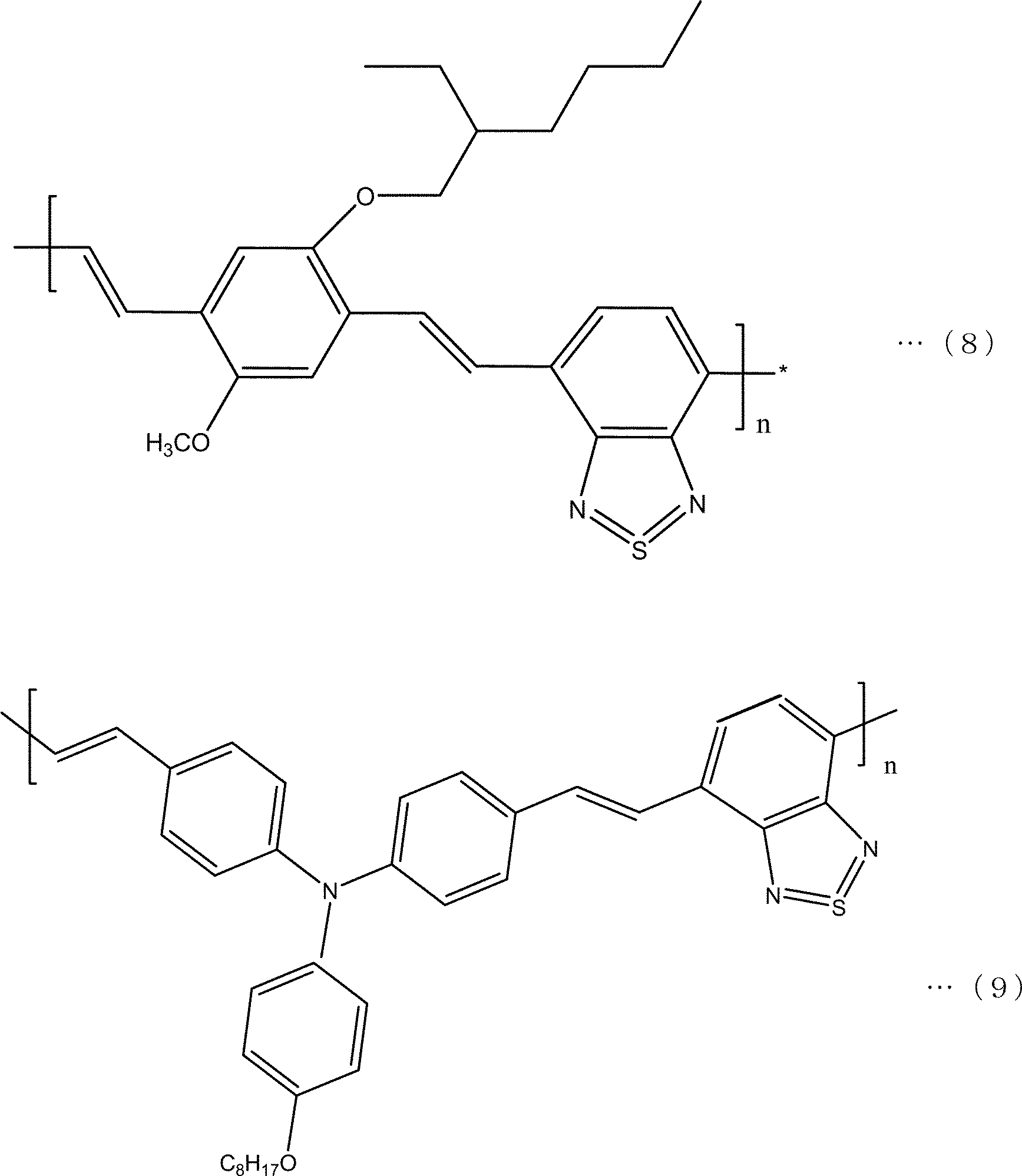
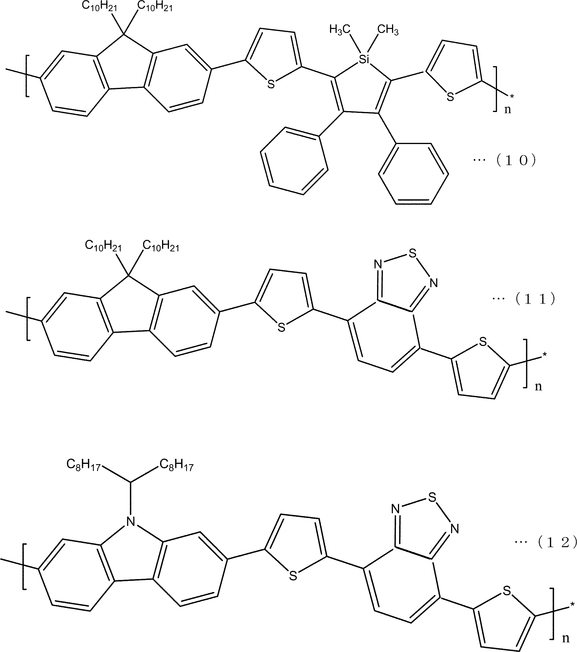
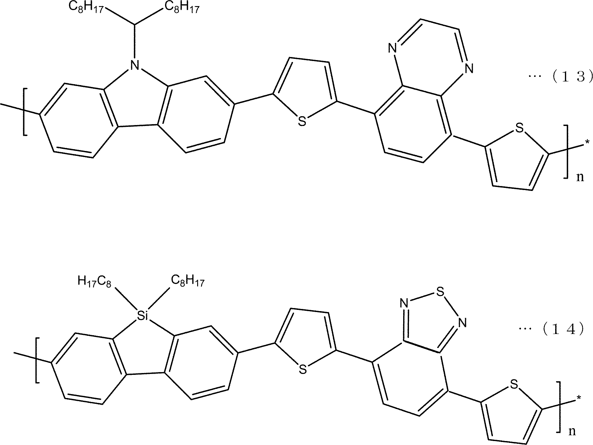
上記式(1)~(14)におけるnは5~150が好ましく、10~100がより好ましい。
上記化合物のうち、式(1)、(6)で表される化合物は、結晶性の化合物である。また、式(7)~(14)で表される化合物は、アモルファス性(非晶性)である。p型有機半導体は、結晶性でもアモルファス性(非晶性)であってもよい。結晶性の有機半導体材料は、ドメインの弾性が高いために、図1に示すような、p型有機半導体のドメイン13aが、バルクヘテロ接合層13中にほぼ均一に分散し、p型有機半導体のドメイン13aによるパーコレーション構造が形成されていない構造のバルクヘテロ接合層13を採り易い。そのため、p型有機半導体は、結晶性の材料が特に好ましく用いられる。また、p型有機半導体の立体規則性の程度については問われない。
p型有機半導体の重量平均分子量は、用いる材料にも依存し、一概には言及出来ないが、2,000~150,000が望ましい。
バルクヘテロ接合層を構成するn型有機半導体としては、電子受容性を有する任意の有機材料を用いることができる。例えば、フラーレン誘導体、ペリレン誘導体等が挙げられる。なかでも、フラーレン誘導体は、p型有機半導体からの電子移動が取り分け早いので、特に好ましい。フラーレン誘導体としては、フラーレンC60の誘導体、フラーレンC70の誘導体、フラーレンC80の誘導体等が好ましく挙げられる。具体的な一例としては、Phenyl-C61-Butyric-Acid-Methyl Ester(PCBM)、Bisadduct-Phenyl-C61-Butyric-Acid-Methyl Ester(bis-PCBM)等が挙げられる。
図1に示す実施形態の有機薄膜太陽電池は、バルクヘテロ接合層13の両側に、第1電極層12、第2電極層14がそれぞれ直接形成されているが、第1電極層12及び第2電極層14のうち、陰極となる電極層と、バルクヘテロ接合層13との間に、正孔ブロック層が形成されていてもよい。この態様によれば、陰極近傍における正孔―電子の再結合を抑制でき、整流性が改善されて短絡電流が向上する。
正孔ブロック層としては、正孔のブロック効果があるものであれば良く、特に限定はない。例えば、フッ化リチウム(LiF)膜、Bathocuproine(BCP)膜、TiOx膜、TiO2膜、ZnOナノパーティクルなどが挙げられる。
正孔ブロック層の膜厚は、0.1nm以上1.0nm以下が好ましく、0.3nm以上0.5nm以下がより好ましい。0.1nm未満であると、正孔のブロック効果が十分に得られない。1.0nmを超えると、絶縁性が高くなって、電荷注入が阻害される傾向にある。
また、第1電極層12及び第2電極層14のうち、陽極となる電極層と、バルクヘテロ接合層13との間に、正孔輸送層が形成されていてもよい。この態様によれば、バルクヘテロ接合層13から陽極への電荷の注入を促進でき、整流性が改善されて短絡電流が向上する。
正孔輸送層としては、poly(3,4-ethylenedioxythiophene/poly(styrene sulfonate)(PEDOT/PSS)等が挙げられる。
次に、本発明の有機薄膜太陽電池の製造方法について説明する。
まず、基板11上に、第1電極層12を形成する。第1電極層12の形成方法としては、特に限定は無く、スパッタ法、CVD法、スプレー成膜法等、従来公知の方法を用いることができる。
次に、第1電極層12上に、直接又は、正孔ブロック層、正孔輸送層等の他の層を介して、p型有機半導体とn型有機半導体と有機溶媒とを含む塗工液を塗布し、塗膜を形成する。
塗工液中におけるp型有機半導体とn型有機半導体との混合割合は、モル比で、p型有機半導体:n型有機半導体=1:0.5~7が好ましく、1:0.7~3がより好ましい。混合割合が上記範囲内であれば、電子と正孔がバランス良く輸送されるため、高いFF値を得ることが出来る。
有機溶媒は、p型有機半導体及びn型有機半導体に対して、十分な溶解性を持つものであることが望ましい。また、有機溶媒の沸点があまり低いと、塗工液の塗布後直ちに溶媒が揮発してしまい、p型有機半導体とn型有機半導体の相分離が十分に進行することが出来ない。本発明者らは、研究の結果、相分離の進行が不十分であると、p型有機半導体のドメインどうしが互いに連結して、パーコレーション構造が形成され易くなることを見出した。そのため、有機溶媒は、一定以上の高い沸点を持つものであることが望ましく、具体的には100℃以上300℃以下が好ましく、120℃以上250℃以下がより好ましい。有機溶媒の好ましい具体例としては、クロロベンゼン(沸点:131℃)、アニソール(沸点:154℃)、1,2-ジクロロベンゼン(沸点:181℃)、1,2,3-トリクロロベンゼン(沸点:221℃)等が挙げられる。
塗工液中における有機溶媒の含有量は、70質量%以上99.9質量%以下が好ましく、80質量%以上99質量%以下がより好ましい。有機溶媒の含有量が70質量%未満であると、溶質である有機半導体同士が凝集して、相分離が生じ難くなる傾向があり、99.9質量%を超えると溶液の粘度が低下して、塗工液の塗布により適切な膜厚を有する塗膜を形成し難くなる。
塗工液には、酸化防止剤、相溶化剤、結晶化促進剤等の添加剤を、物性を損なわない範囲で含有できる。
塗工液の塗布は、乾燥窒素、乾燥アルゴン等の湿度0.01%以下の不活性ガス雰囲気下で行うことが好ましい。酸素や水分の存在下で塗膜を形成すると、これらの成分が塗膜中に残存して、高分子材料を劣化させる恐れがある。
塗工液の塗布方法は、特に限定はなく、スピン塗布、ディップ塗布、スプレー塗布、インクジェット印刷、スクリーン印刷など従来公知の方法を用いることができる。
次に、上記塗工液を塗布して形成した塗膜上に、直接又は、正孔ブロック層、正孔輸送層等の他の層を介して、第2電極層14を形成する。第2電極層14の形成方法としては、特に限定は無く、スパッタ法、CVD法、スプレー成膜法等、従来公知の方法を用いることができる。
そして、本発明では、塗膜上に第2電極層14を形成した後、塗膜を加熱処理してバルクヘテロ接合層13を形成し、有機薄膜太陽電池を製造する。
第2電極層14を形成した後、塗膜を140℃以下の温度で加熱処理することで、詳細な理由は定かではないが、該加熱温度が相図の準安定領域に対応していると推定される理由により、p型有機半導体とn型有機半導体との相分離が十分に進行し、平均直径1nm以上30nm以下のp型有機半導体のドメインが分散しており、かつ、p型有機半導体のドメインどうしが連結して両電極間を接続するパーコレーション構造が形成されていないバルクヘテロ接合層を備えた有機薄膜太陽電池を製造できる。なお、第2電極層14を形成する前に、150℃以上の温度で加熱処理すると、p型有機半導体のドメインどうしが連結して、両電極間を接続するパーコレーション構造が形成される。この理由は、該加熱温度が相図のスピノーダル領域に対応していることによるものと考えられる。
加熱処理方法としては、特に限定は無い。例えば、ホットプレートを用いる方法等が挙げられる。
加熱処理は、塗膜が50℃以上140℃以下になるように加熱し、10分間以上30分間以下行う。温度は100℃以上140℃以下が好ましい。加熱時間は10分間以上20分間以下が好ましい。温度が50℃未満であると、相分離が平衡構造に到達せず、相分離が生じ難い。また、温度が140℃を超えると、p型有機半導体のドメインどうしが連結して両電極間を接続するパーコレーション構造が形成され易くなる。また、加熱時間が10分未満であると相分離が平衡構造に到達せず、相分離が生じ難い。また、30分以上続けても相分離構造はもはや変化しない。
(試験例1)
p型有機半導体としてポリ3-ヘキシルチオフェン(P3HT)を20mgと、n型有機半導体としてPhenyl-C61-Butyric-Acid-Methyl Ester(PCBM)を14mg採取し、溶媒クロロベンゼン(沸点131℃)1mLに溶解させて、20時間攪拌し、塗工液を調製した。
p型有機半導体としてポリ3-ヘキシルチオフェン(P3HT)を20mgと、n型有機半導体としてPhenyl-C61-Butyric-Acid-Methyl Ester(PCBM)を14mg採取し、溶媒クロロベンゼン(沸点131℃)1mLに溶解させて、20時間攪拌し、塗工液を調製した。
第1電極層(ITO)の形成されたガラス基板を用意して、酸素プラズマで表面をドライ洗浄した。その後、スピンコーターを用いて基板上に上記塗工液を塗布し、塗膜を形成した。回転条件は2000rpm×120秒とした。塗布は乾燥窒素が封入されたグローブボックス内で行った。
次に、塗膜上に、第2電極層(Al)を蒸着形成した後に、基板をグローブボックス内に戻し、ホットプレートを用いて加熱処理(130℃×15分)を施してバルクヘテロ接合層を形成し、有機薄膜太陽電池を製造した。
Focused Ion Beam(FIB)を用いて、バルクヘテロ接合層から薄片サンプル(厚み50nm)を切り出し、Scanning Transmission Electron Microscope(STEM)を用いて透過観察を行い、相分離構造を調べた。別に、Electron Energy Loss Spectroscopy(EELS)を用いてバルクヘテロ接合層のドメインの成分を確認した。結果を図2に記す。
図2に示されるように、このバルクヘテロ接合層は、p型有機半導体のドメイン(白色部位)が直径15±5nmの略球状をなしており、バルクヘテロ接合層にほぼ均一に分散していた。また、パーコレーション構造が形成されていなかった。
(試験例2)
試験例1において、加熱処理条件を160℃×15分に変更した以外は、試験例1と同様にしてバルクヘテロ接合層を形成し、有機薄膜太陽電池を製造した。
試験例1において、加熱処理条件を160℃×15分に変更した以外は、試験例1と同様にしてバルクヘテロ接合層を形成し、有機薄膜太陽電池を製造した。
得られた有機薄膜太陽電池について、試験例1と同様にしてFIB、STEM,及びEELSを用い、バルクヘテロ接合層の相分離構造を調べた。結果を図3に記す。
図3に示されるように、より高温で加熱処理して形成したバルクヘテロ接合層は、p型有機半導体のドメイン(白色部位)どうしが連結しており、両電極間を接続するパーコレーション構造が形成されていた。
(試験例3)
試験例1において、塗膜上にLiFを蒸着して正孔ブロック層(厚み0.1nm)を形成し、その正孔ブロック層上に第2電極層(Al)を蒸着形成した。次いで、基板をグローブボックス内に戻し、ホットプレートを用いて加熱処理(160℃×15分)を施してバルクヘテロ接合層を形成し、有機薄膜太陽電池を製造した。
試験例1において、塗膜上にLiFを蒸着して正孔ブロック層(厚み0.1nm)を形成し、その正孔ブロック層上に第2電極層(Al)を蒸着形成した。次いで、基板をグローブボックス内に戻し、ホットプレートを用いて加熱処理(160℃×15分)を施してバルクヘテロ接合層を形成し、有機薄膜太陽電池を製造した。
試験例1~3の有機機薄膜太陽電池の受光セル(2mm×2mm)に、擬似太陽光(AM1.5)を照射して、太陽電池性能(短絡電流(Jsc)、開放電圧(Voc)、FF(曲線因子)、エネルギー変換効率(PCE))を調べた。擬似太陽光の照射には、分光計器製OTE-XLを用いた。電流密度と電圧の測定には、KEITHLEY製2400を用いた。表1に、結果をまとめて記す。

表1に示すように、試験例1は最も高い短絡電流(Jsc)を示した。また、開放電圧(Voc)、FF(曲線因子)、エネルギー変換効率(PCE)についても、試験例1は、正孔ブロック層を形成した試験例3と同程度の太陽電池性能を示した。
11:基板
12:第1電極層
13:バルクヘテロ接合層
13a:p型有機半導体のドメイン
13b:n型有機半導体のドメイン
14:第2電極層
12:第1電極層
13:バルクヘテロ接合層
13a:p型有機半導体のドメイン
13b:n型有機半導体のドメイン
14:第2電極層
Claims (5)
- p型有機半導体のドメインとn型有機半導体のドメインとが相分離しているバルクヘテロ接合層と、前記バルクヘテロ接合層の一方の面側に直接又は他の層を介して配置された陽極と、前記バルクヘテロ接合層の他方の面側に直接又は他の層を介して配置された陰極とを備えた有機薄膜太陽電池であって、
前記バルクヘテロ接合層は、平均直径1nm以上30nm以下のp型有機半導体のドメインが分散しており、かつ、p型有機半導体のドメインどうしが連結して両電極間を接続するパーコレーション構造が形成されていないことを特徴とする有機薄膜太陽電池。 - 前記p型有機半導体のドメインが略球状をなして、前記バルクヘテロ接合層に分散している、請求項1に記載の有機薄膜太陽電池。
- 前記p型有機半導体がアモルファス性材料であり、前記n型半導体がフラーレン誘導体である、請求項1に記載の有機薄膜太陽電池。
- 前記バルクヘテロ接合層と前記陰極との間に、正孔ブロック層が挿入されている、請求項1に記載の有機薄膜太陽電池。
- 基板上に、第1電極層を形成する工程と、
前記第1電極層上に、直接又は他の層を介して、p型有機半導体とn型有機半導体と有機溶媒とを含む塗工液を塗布して塗膜を形成する工程と、
前記塗膜上に、直接又は他の層を介して、第2電極層を形成する工程と、
前記第2電極層を形成したのち、前記塗膜を50℃以上140℃以下で、10分間以上30分間以下加熱処理する工程とを含むことを特徴とする有機薄膜太陽電池の製造方法。
Applications Claiming Priority (2)
| Application Number | Priority Date | Filing Date | Title |
|---|---|---|---|
| JP2012169236A JP2014029904A (ja) | 2012-07-31 | 2012-07-31 | 有機薄膜太陽電池及びその製造方法 |
| JP2012-169236 | 2012-07-31 |
Publications (1)
| Publication Number | Publication Date |
|---|---|
| WO2014020988A1 true WO2014020988A1 (ja) | 2014-02-06 |
Family
ID=50027679
Family Applications (1)
| Application Number | Title | Priority Date | Filing Date |
|---|---|---|---|
| PCT/JP2013/065580 Ceased WO2014020988A1 (ja) | 2012-07-31 | 2013-06-05 | 有機薄膜太陽電池及びその製造方法 |
Country Status (2)
| Country | Link |
|---|---|
| JP (1) | JP2014029904A (ja) |
| WO (1) | WO2014020988A1 (ja) |
Cited By (1)
| Publication number | Priority date | Publication date | Assignee | Title |
|---|---|---|---|---|
| EP3410507A4 (en) * | 2016-03-11 | 2019-03-27 | LG Chem, Ltd. | ORGANIC SOLAR CELL AND METHOD FOR THE PRODUCTION THEREOF |
Families Citing this family (3)
| Publication number | Priority date | Publication date | Assignee | Title |
|---|---|---|---|---|
| DE112018005911T5 (de) * | 2017-11-20 | 2020-07-30 | Sony Corporation | Photoelektrisches umwandlungselement und festkörper-bildaufnahmevorrichtung |
| JP2020188231A (ja) * | 2019-05-17 | 2020-11-19 | ソニー株式会社 | 光電変換素子および撮像装置 |
| US20230157040A1 (en) * | 2020-06-19 | 2023-05-18 | Sony Group Corporation | Photoelectric conversion element and imaging device |
Citations (3)
| Publication number | Priority date | Publication date | Assignee | Title |
|---|---|---|---|---|
| JP2004165474A (ja) * | 2002-11-14 | 2004-06-10 | Matsushita Electric Ind Co Ltd | 光電変換素子及びその製造方法 |
| JP2011155154A (ja) * | 2010-01-27 | 2011-08-11 | Fujifilm Corp | 透明導電フィルム、その製造方法及び有機薄膜太陽電池 |
| JP2011222903A (ja) * | 2010-04-14 | 2011-11-04 | Kinyosha Co Ltd | 有機薄膜太陽電池の製造方法 |
-
2012
- 2012-07-31 JP JP2012169236A patent/JP2014029904A/ja active Pending
-
2013
- 2013-06-05 WO PCT/JP2013/065580 patent/WO2014020988A1/ja not_active Ceased
Patent Citations (3)
| Publication number | Priority date | Publication date | Assignee | Title |
|---|---|---|---|---|
| JP2004165474A (ja) * | 2002-11-14 | 2004-06-10 | Matsushita Electric Ind Co Ltd | 光電変換素子及びその製造方法 |
| JP2011155154A (ja) * | 2010-01-27 | 2011-08-11 | Fujifilm Corp | 透明導電フィルム、その製造方法及び有機薄膜太陽電池 |
| JP2011222903A (ja) * | 2010-04-14 | 2011-11-04 | Kinyosha Co Ltd | 有機薄膜太陽電池の製造方法 |
Cited By (2)
| Publication number | Priority date | Publication date | Assignee | Title |
|---|---|---|---|---|
| EP3410507A4 (en) * | 2016-03-11 | 2019-03-27 | LG Chem, Ltd. | ORGANIC SOLAR CELL AND METHOD FOR THE PRODUCTION THEREOF |
| US10672985B2 (en) | 2016-03-11 | 2020-06-02 | Lg Chem, Ltd. | Organic solar cell and method for manufacturing same |
Also Published As
| Publication number | Publication date |
|---|---|
| JP2014029904A (ja) | 2014-02-13 |
Similar Documents
| Publication | Publication Date | Title |
|---|---|---|
| Miao et al. | A non-fullerene small molecule processed with green solvent as an electron transporting material for high efficiency pin perovskite solar cells | |
| Xie et al. | Improved performance and air stability of planar perovskite solar cells via interfacial engineering using a fullerene amine interlayer | |
| Liu et al. | Fluorinated fused nonacyclic interfacial materials for efficient and stable perovskite solar cells | |
| Li et al. | Achieving efficient thick film all-polymer solar cells using a green solvent additive | |
| Tan et al. | Chemical linkage and passivation at buried interface for thermally stable inverted perovskite solar cells with efficiency over 22% | |
| US20100147386A1 (en) | Doped interfacial modification layers for stability enhancement for bulk heterojunction organic solar cells | |
| Aryal et al. | Highly efficient polyacetylene–based polyelectrolytes as cathode interfacial layers for organic solar cell applications | |
| Shin et al. | Electronic structure of nonionic surfactant-modified PEDOT: PSS and its application in perovskite solar cells with reduced interface recombination | |
| CN103236503B (zh) | 一种聚合物太阳能电池及其制备方法 | |
| Aslan et al. | Sol–gel derived In2S3 buffer layers for inverted organic photovoltaic cells | |
| Ryu et al. | Effect of solution processed graphene oxide/nickel oxide bi-layer on cell performance of bulk-heterojunction organic photovoltaic | |
| JP2019054142A (ja) | 光電変換素子、その製造方法、およびその製造装置 | |
| Kim et al. | A Thiophene based dopant-free hole-transport polymer for efficient and stable perovskite solar cells | |
| Ge et al. | Core-expanded naphthalenediimide derivatives as non-fullerene electron transport materials for inverted perovskite solar cells | |
| Yu et al. | Optimization of the energy level alignment between the photoactive layer and the cathode contact utilizing solution-processed hafnium acetylacetonate as buffer layer for efficient polymer solar cells | |
| Shah et al. | Optimization of active-layer thickness, top electrode and annealing temperature for polymeric solar cells | |
| JP5444743B2 (ja) | 有機光電変換素子 | |
| WO2014020988A1 (ja) | 有機薄膜太陽電池及びその製造方法 | |
| Park et al. | Water-processable electron-collecting layers of a hybrid poly (ethylene oxide): Caesium carbonate composite for flexible inverted polymer solar cells | |
| Zhang et al. | Efficient ternary organic solar cells with small aggregation phases and low bimolecular recombination using ICBA: ITIC double electron acceptors | |
| US20130328018A1 (en) | Fluorine-modification process and applications thereof | |
| WO2014020989A1 (ja) | 有機薄膜太陽電池の製造方法 | |
| CN104011892B (zh) | 高聚物太阳能电池器件及其制备方法 | |
| Lampande et al. | Solution processed n-type mixed metal oxide layer for electron extraction in inverted polymer solar cells | |
| Li et al. | Improving electron transport by using a NaCl/Polyethylenimine ethoxylated double layer for high-efficiency polymer solar cells |
Legal Events
| Date | Code | Title | Description |
|---|---|---|---|
| 121 | Ep: the epo has been informed by wipo that ep was designated in this application |
Ref document number: 13824751 Country of ref document: EP Kind code of ref document: A1 |
|
| NENP | Non-entry into the national phase |
Ref country code: DE |
|
| 122 | Ep: pct application non-entry in european phase |
Ref document number: 13824751 Country of ref document: EP Kind code of ref document: A1 |