WO2014017148A1 - 積層研磨パッド及びその製造方法 - Google Patents
積層研磨パッド及びその製造方法 Download PDFInfo
- Publication number
- WO2014017148A1 WO2014017148A1 PCT/JP2013/063894 JP2013063894W WO2014017148A1 WO 2014017148 A1 WO2014017148 A1 WO 2014017148A1 JP 2013063894 W JP2013063894 W JP 2013063894W WO 2014017148 A1 WO2014017148 A1 WO 2014017148A1
- Authority
- WO
- WIPO (PCT)
- Prior art keywords
- layer
- polishing
- laminated
- polishing pad
- melt adhesive
- Prior art date
- Legal status (The legal status is an assumption and is not a legal conclusion. Google has not performed a legal analysis and makes no representation as to the accuracy of the status listed.)
- Ceased
Links
Images

Classifications
-
- H—ELECTRICITY
- H10—SEMICONDUCTOR DEVICES; ELECTRIC SOLID-STATE DEVICES NOT OTHERWISE PROVIDED FOR
- H10P—GENERIC PROCESSES OR APPARATUS FOR THE MANUFACTURE OR TREATMENT OF DEVICES COVERED BY CLASS H10
- H10P52/00—Grinding, lapping or polishing of wafers, substrates or parts of devices
-
- B—PERFORMING OPERATIONS; TRANSPORTING
- B24—GRINDING; POLISHING
- B24B—MACHINES, DEVICES, OR PROCESSES FOR GRINDING OR POLISHING; DRESSING OR CONDITIONING OF ABRADING SURFACES; FEEDING OF GRINDING, POLISHING, OR LAPPING AGENTS
- B24B37/00—Lapping machines or devices; Accessories
- B24B37/11—Lapping tools
- B24B37/20—Lapping pads for working plane surfaces
- B24B37/22—Lapping pads for working plane surfaces characterised by a multi-layered structure
-
- B—PERFORMING OPERATIONS; TRANSPORTING
- B24—GRINDING; POLISHING
- B24B—MACHINES, DEVICES, OR PROCESSES FOR GRINDING OR POLISHING; DRESSING OR CONDITIONING OF ABRADING SURFACES; FEEDING OF GRINDING, POLISHING, OR LAPPING AGENTS
- B24B37/00—Lapping machines or devices; Accessories
- B24B37/11—Lapping tools
- B24B37/20—Lapping pads for working plane surfaces
- B24B37/26—Lapping pads for working plane surfaces characterised by the shape of the lapping pad surface, e.g. grooved
-
- B—PERFORMING OPERATIONS; TRANSPORTING
- B32—LAYERED PRODUCTS
- B32B—LAYERED PRODUCTS, i.e. PRODUCTS BUILT-UP OF STRATA OF FLAT OR NON-FLAT, e.g. CELLULAR OR HONEYCOMB, FORM
- B32B27/00—Layered products comprising a layer of synthetic resin
- B32B27/06—Layered products comprising a layer of synthetic resin as the main or only constituent of a layer, which is next to another layer of the same or of a different material
- B32B27/065—Layered products comprising a layer of synthetic resin as the main or only constituent of a layer, which is next to another layer of the same or of a different material of foam
-
- B—PERFORMING OPERATIONS; TRANSPORTING
- B32—LAYERED PRODUCTS
- B32B—LAYERED PRODUCTS, i.e. PRODUCTS BUILT-UP OF STRATA OF FLAT OR NON-FLAT, e.g. CELLULAR OR HONEYCOMB, FORM
- B32B27/00—Layered products comprising a layer of synthetic resin
- B32B27/36—Layered products comprising a layer of synthetic resin comprising polyesters
-
- B—PERFORMING OPERATIONS; TRANSPORTING
- B32—LAYERED PRODUCTS
- B32B—LAYERED PRODUCTS, i.e. PRODUCTS BUILT-UP OF STRATA OF FLAT OR NON-FLAT, e.g. CELLULAR OR HONEYCOMB, FORM
- B32B37/00—Methods or apparatus for laminating, e.g. by curing or by ultrasonic bonding
- B32B37/12—Methods or apparatus for laminating, e.g. by curing or by ultrasonic bonding characterised by using adhesives
- B32B37/1207—Heat-activated adhesive
-
- B—PERFORMING OPERATIONS; TRANSPORTING
- B32—LAYERED PRODUCTS
- B32B—LAYERED PRODUCTS, i.e. PRODUCTS BUILT-UP OF STRATA OF FLAT OR NON-FLAT, e.g. CELLULAR OR HONEYCOMB, FORM
- B32B37/00—Methods or apparatus for laminating, e.g. by curing or by ultrasonic bonding
- B32B37/14—Methods or apparatus for laminating, e.g. by curing or by ultrasonic bonding characterised by the properties of the layers
- B32B37/16—Methods or apparatus for laminating, e.g. by curing or by ultrasonic bonding characterised by the properties of the layers with all layers existing as coherent layers before laminating
- B32B37/18—Methods or apparatus for laminating, e.g. by curing or by ultrasonic bonding characterised by the properties of the layers with all layers existing as coherent layers before laminating involving the assembly of discrete sheets or panels only
-
- B—PERFORMING OPERATIONS; TRANSPORTING
- B32—LAYERED PRODUCTS
- B32B—LAYERED PRODUCTS, i.e. PRODUCTS BUILT-UP OF STRATA OF FLAT OR NON-FLAT, e.g. CELLULAR OR HONEYCOMB, FORM
- B32B37/00—Methods or apparatus for laminating, e.g. by curing or by ultrasonic bonding
- B32B37/14—Methods or apparatus for laminating, e.g. by curing or by ultrasonic bonding characterised by the properties of the layers
- B32B37/16—Methods or apparatus for laminating, e.g. by curing or by ultrasonic bonding characterised by the properties of the layers with all layers existing as coherent layers before laminating
- B32B37/20—Methods or apparatus for laminating, e.g. by curing or by ultrasonic bonding characterised by the properties of the layers with all layers existing as coherent layers before laminating involving the assembly of continuous webs only
- B32B37/203—One or more of the layers being plastic
-
- B—PERFORMING OPERATIONS; TRANSPORTING
- B32—LAYERED PRODUCTS
- B32B—LAYERED PRODUCTS, i.e. PRODUCTS BUILT-UP OF STRATA OF FLAT OR NON-FLAT, e.g. CELLULAR OR HONEYCOMB, FORM
- B32B38/00—Ancillary operations in connection with laminating processes
- B32B38/0004—Cutting, tearing or severing, e.g. bursting; Cutter details
-
- B—PERFORMING OPERATIONS; TRANSPORTING
- B32—LAYERED PRODUCTS
- B32B—LAYERED PRODUCTS, i.e. PRODUCTS BUILT-UP OF STRATA OF FLAT OR NON-FLAT, e.g. CELLULAR OR HONEYCOMB, FORM
- B32B7/00—Layered products characterised by the relation between layers; Layered products characterised by the relative orientation of features between layers, or by the relative values of a measurable parameter between layers, i.e. products comprising layers having different physical, chemical or physicochemical properties; Layered products characterised by the interconnection of layers
- B32B7/04—Interconnection of layers
- B32B7/12—Interconnection of layers using interposed adhesives or interposed materials with bonding properties
-
- B—PERFORMING OPERATIONS; TRANSPORTING
- B32—LAYERED PRODUCTS
- B32B—LAYERED PRODUCTS, i.e. PRODUCTS BUILT-UP OF STRATA OF FLAT OR NON-FLAT, e.g. CELLULAR OR HONEYCOMB, FORM
- B32B37/00—Methods or apparatus for laminating, e.g. by curing or by ultrasonic bonding
- B32B37/12—Methods or apparatus for laminating, e.g. by curing or by ultrasonic bonding characterised by using adhesives
- B32B37/1207—Heat-activated adhesive
- B32B2037/1215—Hot-melt adhesive
-
- B—PERFORMING OPERATIONS; TRANSPORTING
- B32—LAYERED PRODUCTS
- B32B—LAYERED PRODUCTS, i.e. PRODUCTS BUILT-UP OF STRATA OF FLAT OR NON-FLAT, e.g. CELLULAR OR HONEYCOMB, FORM
- B32B37/00—Methods or apparatus for laminating, e.g. by curing or by ultrasonic bonding
- B32B37/12—Methods or apparatus for laminating, e.g. by curing or by ultrasonic bonding characterised by using adhesives
- B32B37/1207—Heat-activated adhesive
- B32B2037/1215—Hot-melt adhesive
- B32B2037/1223—Hot-melt adhesive film-shaped
-
- B—PERFORMING OPERATIONS; TRANSPORTING
- B32—LAYERED PRODUCTS
- B32B—LAYERED PRODUCTS, i.e. PRODUCTS BUILT-UP OF STRATA OF FLAT OR NON-FLAT, e.g. CELLULAR OR HONEYCOMB, FORM
- B32B2266/00—Composition of foam
- B32B2266/02—Organic
- B32B2266/0214—Materials belonging to B32B27/00
- B32B2266/0278—Polyurethane
-
- B—PERFORMING OPERATIONS; TRANSPORTING
- B32—LAYERED PRODUCTS
- B32B—LAYERED PRODUCTS, i.e. PRODUCTS BUILT-UP OF STRATA OF FLAT OR NON-FLAT, e.g. CELLULAR OR HONEYCOMB, FORM
- B32B2305/00—Condition, form or state of the layers or laminate
- B32B2305/02—Cellular or porous
- B32B2305/022—Foam
-
- B—PERFORMING OPERATIONS; TRANSPORTING
- B32—LAYERED PRODUCTS
- B32B—LAYERED PRODUCTS, i.e. PRODUCTS BUILT-UP OF STRATA OF FLAT OR NON-FLAT, e.g. CELLULAR OR HONEYCOMB, FORM
- B32B2307/00—Properties of the layers or laminate
- B32B2307/70—Other properties
- B32B2307/704—Crystalline
-
- B—PERFORMING OPERATIONS; TRANSPORTING
- B32—LAYERED PRODUCTS
- B32B—LAYERED PRODUCTS, i.e. PRODUCTS BUILT-UP OF STRATA OF FLAT OR NON-FLAT, e.g. CELLULAR OR HONEYCOMB, FORM
- B32B2457/00—Electrical equipment
- B32B2457/14—Semiconductor wafers
-
- B—PERFORMING OPERATIONS; TRANSPORTING
- B32—LAYERED PRODUCTS
- B32B—LAYERED PRODUCTS, i.e. PRODUCTS BUILT-UP OF STRATA OF FLAT OR NON-FLAT, e.g. CELLULAR OR HONEYCOMB, FORM
- B32B2551/00—Optical elements
-
- B—PERFORMING OPERATIONS; TRANSPORTING
- B32—LAYERED PRODUCTS
- B32B—LAYERED PRODUCTS, i.e. PRODUCTS BUILT-UP OF STRATA OF FLAT OR NON-FLAT, e.g. CELLULAR OR HONEYCOMB, FORM
- B32B38/00—Ancillary operations in connection with laminating processes
- B32B38/04—Punching, slitting or perforating
-
- Y—GENERAL TAGGING OF NEW TECHNOLOGICAL DEVELOPMENTS; GENERAL TAGGING OF CROSS-SECTIONAL TECHNOLOGIES SPANNING OVER SEVERAL SECTIONS OF THE IPC; TECHNICAL SUBJECTS COVERED BY FORMER USPC CROSS-REFERENCE ART COLLECTIONS [XRACs] AND DIGESTS
- Y10—TECHNICAL SUBJECTS COVERED BY FORMER USPC
- Y10T—TECHNICAL SUBJECTS COVERED BY FORMER US CLASSIFICATION
- Y10T156/00—Adhesive bonding and miscellaneous chemical manufacture
- Y10T156/10—Methods of surface bonding and/or assembly therefor
- Y10T156/1052—Methods of surface bonding and/or assembly therefor with cutting, punching, tearing or severing
-
- Y—GENERAL TAGGING OF NEW TECHNOLOGICAL DEVELOPMENTS; GENERAL TAGGING OF CROSS-SECTIONAL TECHNOLOGIES SPANNING OVER SEVERAL SECTIONS OF THE IPC; TECHNICAL SUBJECTS COVERED BY FORMER USPC CROSS-REFERENCE ART COLLECTIONS [XRACs] AND DIGESTS
- Y10—TECHNICAL SUBJECTS COVERED BY FORMER USPC
- Y10T—TECHNICAL SUBJECTS COVERED BY FORMER US CLASSIFICATION
- Y10T156/00—Adhesive bonding and miscellaneous chemical manufacture
- Y10T156/10—Methods of surface bonding and/or assembly therefor
- Y10T156/1052—Methods of surface bonding and/or assembly therefor with cutting, punching, tearing or severing
- Y10T156/1082—Partial cutting bonded sandwich [e.g., grooving or incising]
Definitions
- the present invention stabilizes flattening processing of optical materials such as lenses and reflecting mirrors, silicon wafers, glass substrates for hard disks, aluminum substrates, and materials that require high surface flatness such as general metal polishing processing
- the present invention also relates to a laminated polishing pad that can be performed with high polishing efficiency and a method for manufacturing the same.
- the laminated polishing pad of the present invention is particularly suitable for a step of planarizing a silicon wafer and a device having an oxide layer, a metal layer, etc. formed thereon, before further laminating and forming these oxide layers and metal layers. Preferably used.
- a step of forming a conductive layer on the wafer surface and forming a wiring layer by photolithography, etching, or the like, or a step of forming an interlayer insulating film on the wiring layer cause irregularities made of a conductor such as metal or an insulator on the wafer surface.
- miniaturization of wiring and multilayer wiring have been advanced for the purpose of increasing the density of semiconductor integrated circuits, and along with this, technology for flattening the irregularities on the wafer surface has become important.
- CMP chemical mechanical polishing
- slurry a slurry-like abrasive
- abrasive grains are dispersed in a state where the surface to be polished of a wafer is pressed against the polishing surface of a polishing pad.
- a polishing apparatus generally used in CMP includes a polishing surface plate 2 that supports a polishing pad 1 and a support base (polishing head) 5 that supports a material to be polished (semiconductor wafer) 4.
- the polishing pad 1 is attached to the polishing surface plate 2 by attaching it with a double-sided tape, for example.
- the polishing surface plate 2 and the support base 5 are disposed so that the polishing pad 1 and the material to be polished 4 supported by each of the polishing surface plate 2 and the support base 5 are opposed to each other, and are provided with rotating shafts 6 and 7 respectively. Further, a pressurizing mechanism for pressing the workpiece 4 against the polishing pad 1 is provided on the support base 5 side.
- a polyurethane resin foam sheet is generally used as a polishing pad used for high-precision polishing.
- the polyurethane resin foam sheet is excellent in local flattening ability, it is difficult to apply a uniform pressure to the entire wafer surface because of insufficient cushioning properties. For this reason, usually, a soft cushion layer is separately provided on the back surface of the polyurethane resin foam sheet, and is used for polishing as a laminated polishing pad.
- conventional laminated polishing pads generally have a polishing layer and a cushion layer bonded to each other with a double-sided tape, but the slurry enters between the polishing layer and the cushion layer during polishing, reducing the durability of the double-sided tape.
- the polishing layer and the cushion layer are easily peeled off.
- Patent Document 1 discloses that a plastic film and a polishing pad are bonded using a reactive hot melt adhesive.
- Patent Document 2 discloses a polishing pad in which a base layer and a polishing layer are bonded by a hot melt adhesive layer.
- a hot-melt adhesive layer for laminating a hard pad main body is formed on one side of a base material, and a pressure-sensitive adhesive layer for laminating a cushioning subpad is formed on the other side.
- the hot-melt adhesive layer of the double-sided pressure-sensitive adhesive tape for a multi-layer polishing pad is heated to laminate the hard pad body on one side of the substrate via the hot-melt adhesive layer, and then the pressure-sensitive adhesive
- a method for producing a multi-layer polishing pad is disclosed, in which a cushioning subpad is pressed onto the agent layer, and the cushioning subpad is laminated on the other surface of the substrate via the pressure-sensitive adhesive layer.
- Patent Document 4 discloses a polishing pad in which a polishing layer and a base layer are bonded to each other by a double-sided tape.
- the polishing pad is made of a hot-melt adhesive between the back surface of the polishing layer and the double-sided tape and blocks the polishing slurry.
- a technique for providing a water blocking layer is disclosed.
- Patent Document 5 discloses a polishing pad in which a polishing layer and a lower layer are bonded by a hot melt adhesive containing EVA.
- Patent Document 6 provides a polishing layer; Providing a subpad layer having a top surface and a bottom surface; Providing an uncured reactive hot melt adhesive; Applying an uncured reactive hot melt adhesive to the upper surface of the subpad layer in a parallel line pattern; Placing a polishing layer on a parallel line pattern of uncured reactive hot melt adhesive to form a polishing pad laminate; Applying force to the polishing pad laminate to press the polishing layer and the subpad layer; and curing the uncured reactive hot melt adhesive to bond the reactive hot melt adhesive between the polishing layer and the subpad layer Form; A method for manufacturing a multi-layer chemical mechanical polishing pad is disclosed.
- Delamination can be prevented by using a hot melt adhesive.
- a hot melt adhesive using a laminate roll on a continuous line
- the cushion layer is likely to be wrinkled.
- JP 2002-224944 A JP 2005-167200 A JP 2006-265410 A JP 2009-95945 A Japanese translation of PCT publication 2010-52595 JP 2010-28113 A
- An object of the present invention is to provide a method for producing a laminated polishing pad that is difficult to peel between the polishing layer and the support layer even when the temperature becomes high due to long-time polishing and that the support layer is less likely to be wrinkled.
- the present inventors have found that the above object can be achieved by the following method for producing a laminated polishing pad, and have completed the present invention.
- a laminate in which a polishing layer and a support layer are laminated via a hot-melt adhesive member is passed between a pair of laminate rolls, and the polishing layer and the support layer are bonded together with a hot-melt adhesive member.
- the ratio (TD1 / TD2) between the length of the polishing layer in the TD direction (TD1) and the length of the support layer in the TD direction (TD2) (TD1 / TD2) is always adjusted to 0.3 or more.
- the present invention relates to a manufacturing method of a featured laminated polishing pad.
- a polishing layer and a support layer are bonded together with a hot-melt adhesive using a laminate roll on a continuous line
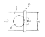
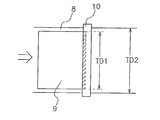
- a hot-melt adhesive (not shown) is provided, and then a circular polishing layer 9 is laminated on the hot-melt adhesive, and the resulting laminate is passed between a pair of laminating rolls 10 to polish the polishing layer 9.
- the support layer 8 were bonded together with a hot melt adhesive.
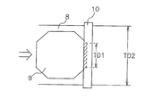
- the inventor always sets the ratio (TD1 / TD2) of the length (TD1) of the polishing layer 9 in the TD direction to the length (TD2) of the support layer 8 in the TD direction.
- the pressure By adjusting the pressure to 0.3 or more and uniformly applying linear pressure to the support layer portion (shaded portions in FIGS. 3 and 4) on which the polishing layer 9 is laminated, the support layer 8 after bonding is less likely to be wrinkled.
- FIG. 2 when the circular polishing layer 9 is used, or when TD1 / TD2 is less than 0.3, it is difficult to prevent the generation of wrinkles.
- the method for producing a laminated polishing pad of the present invention may include a step of cutting the laminated abrasive sheet into a circle. In the case of manufacturing a circular laminated polishing pad, it is necessary to produce a laminated abrasive sheet and then cut it into a circle.
- the method for producing a laminated polishing pad according to the present invention may include a step of grooving the surface of the laminated abrasive sheet.
- the hot melt adhesive member is an adhesive layer containing a polyester hot melt adhesive, or a double-sided tape having the adhesive layer on both sides of a base material, and the polyester hot melt adhesive is a base polymer. It is preferable to contain 2 to 10 parts by weight of an epoxy resin having two or more glycidyl groups in one molecule with respect to 100 parts by weight of the polyester resin.
- the polyester resin By adding 2 to 10 parts by weight of an epoxy resin having two or more glycidyl groups in one molecule with respect to 100 parts by weight of the polyester resin as a base polymer, the polyester resin is cross-linked so that a high temperature can be obtained by long-time polishing. Even in this case, the durability of the adhesive member against “slipping” generated during polishing is improved, and a laminated polishing pad that does not easily peel between the polishing layer and the support layer is obtained.
- the addition amount of the epoxy resin is less than 2 parts by weight, the durability of the adhesive member against “slipping” generated during polishing becomes insufficient when the temperature becomes high due to long-time polishing. It becomes easy to peel between layers.
- it exceeds 10 parts by weight the hardness of the adhesive layer becomes too high and the adhesiveness is lowered, so that it is easy to peel between the polishing layer and the support layer.
- the polyester resin as the base polymer is preferably a crystalline polyester resin.
- the chemical resistance to the slurry is improved, and the adhesive force of the adhesive layer is hardly lowered.
- the present invention relates to a laminated polishing pad obtained by the production method and a method for producing a semiconductor device including a step of polishing a surface of a semiconductor wafer using the laminated polishing pad.
- the laminated polishing pad having no wrinkle on the support layer is obtained. Obtainable.
- the polishing layer and the support layer are laminated via an adhesive member containing a specific polyester-based hot melt adhesive. However, it is difficult to peel between the polishing layer and the support layer.
- Schematic configuration diagram showing an example of a polishing apparatus used in CMP polishing Schematic showing an example of a conventional method for manufacturing a laminated polishing pad
- Schematic which shows an example of the manufacturing method of the lamination
- Schematic which shows an example of the manufacturing method of the lamination
- a laminate in which a polishing layer and a support layer are laminated via a hot-melt adhesive member is passed between a pair of laminate rolls, and the polishing layer and the support layer are made into a hot-melt type. It includes a step of producing a laminated abrasive sheet by bonding with an adhesive member.
- the polishing layer is not particularly limited as long as it is a foam having fine bubbles.
- polyurethane resin polyurethane resin, polyester resin, polyamide resin, acrylic resin, polycarbonate resin, halogen resin (polyvinyl chloride, polytetrafluoroethylene, polyvinylidene fluoride, etc.), polystyrene, olefin resin (polyethylene, polypropylene, etc.), epoxy resin 1 type, or 2 or more types of mixtures, such as a photosensitive resin, is mentioned.
- Polyurethane resin is a particularly preferable material for forming the polishing layer because it has excellent wear resistance and a polymer having desired physical properties can be easily obtained by variously changing the raw material composition.
- the polyurethane resin will be described on behalf of the foam.
- the polyurethane resin is composed of an isocyanate component, a polyol component (high molecular weight polyol, low molecular weight polyol), and a chain extender.
- the isocyanate component a known compound in the field of polyurethane can be used without particular limitation.
- the isocyanate component 2,4-toluene diisocyanate, 2,6-toluene diisocyanate, 2,2′-diphenylmethane diisocyanate, 2,4′-diphenylmethane diisocyanate, 4,4′-diphenylmethane diisocyanate, 1,5-naphthalene diisocyanate, aromatic diisocyanates such as p-phenylene diisocyanate, m-phenylene diisocyanate, p-xylylene diisocyanate, m-xylylene diisocyanate; ethylene diisocyanate, 2,2,4-trimethylhexamethylene diisocyanate, 1,6-hexamethylene diisocyanate, etc.
- Aliphatic diisocyanate 1,4-cyclohexane diisocyanate, 4,4'-dicyclohexylmethane diisocyanate, isophorone diisocyanate Isocyanate, alicyclic diisocyanates such as norbornane diisocyanate. These may be used alone or in combination of two or more.
- Examples of the high molecular weight polyol include those usually used in the technical field of polyurethane. Examples include polyether polyols typified by polytetramethylene ether glycol, polyethylene glycol, etc., polyester polyols typified by polybutylene adipate, polycaprolactone polyols, reactants of polyester glycols such as polycaprolactone and alkylene carbonate, etc. Polyester polycarbonate polyol obtained by reacting ethylene carbonate with polyhydric alcohol and then reacting the obtained reaction mixture with organic dicarboxylic acid, polycarbonate polyol obtained by transesterification of polyhydroxyl compound and aryl carbonate Etc. These may be used alone or in combination of two or more.
- low molecular weight polyamines such as ethylenediamine, tolylenediamine, diphenylmethanediamine, and diethylenetriamine
- alcohol amines such as monoethanolamine, 2- (2-aminoethylamino) ethanol, and monopropanolamine can be used in combination.
- These low molecular weight polyols and low molecular weight polyamines may be used alone or in combination of two or more.
- the blending amount of the low molecular weight polyol, the low molecular weight polyamine or the like is not particularly limited, and is appropriately determined depending on the properties required for the polishing pad (polishing layer) to be produced.
- a chain extender is used for curing the prepolymer.
- the chain extender is an organic compound having at least two active hydrogen groups, and examples of the active hydrogen group include a hydroxyl group, a primary or secondary amino group, and a thiol group (SH).
- the polyurethane resin foam can be produced by applying a known urethanization technique such as a melting method or a solution method, but is preferably produced by a melting method in consideration of cost, working environment, and the like.
- the polyurethane resin foam can be produced by either the prepolymer method or the one-shot method.
- an isocyanate-terminated prepolymer is synthesized beforehand from an isocyanate component and a polyol component, and this is reacted with a chain extender.
- the polymer method is preferred because the resulting polyurethane resin has excellent physical properties.
- Examples of the method for producing a polyurethane resin foam include a method of adding hollow beads, a mechanical foaming method, and a chemical foaming method.
- a mechanical foaming method using a silicon surfactant which is a copolymer of polyalkylsiloxane and polyether and does not have an active hydrogen group is preferable.
- stabilizers such as antioxidants, lubricants, pigments, fillers, antistatic agents, and other additives may be added.
- the polyurethane resin foam may be a closed cell type or an open cell type.
- the average cell diameter of the polyurethane resin foam is preferably 30 to 80 ⁇ m, more preferably 30 to 60 ⁇ m. When deviating from this range, the polishing rate tends to decrease, or the planarity of the polished material (wafer) after polishing tends to decrease.
- the specific gravity of the polyurethane resin foam is preferably 0.5 to 1.3.
- the specific gravity is less than 0.5, the surface strength of the polishing layer decreases, and the planarity of the material to be polished tends to decrease.
- the ratio is larger than 1.3, the number of bubbles on the surface of the polishing layer is reduced and planarity is good, but the polishing rate tends to decrease.
- the hardness of the polyurethane resin foam is preferably 40 to 75 degrees as measured by an Asker D hardness meter.
- Asker D hardness is less than 40 degrees, the planarity of the material to be polished is lowered, and when it is larger than 75 degrees, the planarity is good, but the uniformity (uniformity) of the material to be polished is lowered. There is a tendency.
- the thickness of the polishing layer is not particularly limited, but is usually about 0.8 to 4 mm, preferably 1.2 to 2.5 mm.
- the support layer supplements the characteristics of the polishing layer.
- a layer having a lower elastic modulus than the polishing layer (cushion layer) may be used, or a layer having a higher elastic modulus than the polishing layer (high elastic layer) may be used.
- the cushion layer is necessary in order to achieve both planarity and uniformity in a trade-off relationship in CMP.
- Planarity refers to the flatness of a pattern portion when a material having fine irregularities generated during pattern formation is polished
- uniformity refers to the uniformity of the entire material to be polished. The planarity is improved by the characteristics of the polishing layer, and the uniformity is improved by the characteristics of the cushion layer.
- the high elastic layer is used for improving the planarization characteristics of the polishing pad when a soft polishing layer is used in CMP to suppress the occurrence of scratches.
- a highly elastic layer it is possible to suppress excessive cutting of the edge portion of the material to be polished.
- the cushion layer examples include fiber nonwoven fabrics such as polyester nonwoven fabric, nylon nonwoven fabric, and acrylic nonwoven fabric; resin-impregnated nonwoven fabrics such as polyester nonwoven fabric impregnated with polyurethane; polymer resin foams such as polyurethane foam and polyethylene foam; butadiene rubber and Examples thereof include rubber resins such as isoprene rubber; and photosensitive resins.
- the thickness of the cushion layer is not particularly limited, but is preferably 300 to 1800 ⁇ m, more preferably 700 to 1400 ⁇ m.
- Examples of the highly elastic layer include a metal sheet and a resin film.
- Examples of the resin film include polyester films such as polyethylene terephthalate film and polyethylene naphthalate film; polyolefin films such as polyethylene film and polypropylene film; nylon film; polyimide film and the like.
- the thickness of the highly elastic layer is not particularly limited, but is preferably 10 to 200 ⁇ m, more preferably 15 to 55 ⁇ m from the viewpoints of rigidity and dimensional stability during heating.
- the laminate is prepared by laminating a polishing layer and a support layer via a hot-melt adhesive member.
- an adhesive layer containing a general hot-melt adhesive can be used, but an adhesive layer containing a polyester-based hot-melt adhesive is particularly preferred.
- the polyester-based hot melt adhesive contains at least a polyester resin as a base polymer and an epoxy resin having two or more glycidyl groups in one molecule as a crosslinking component.
- polyester resin known ones obtained by condensation polymerization of an acid component and a polyol component can be used, and it is particularly preferable to use a crystalline polyester resin.
- the acid component examples include aromatic dicarboxylic acids, aliphatic dicarboxylic acids, and alicyclic dicarboxylic acids. These may be used alone or in combination of two or more.
- aromatic dicarboxylic acid examples include terephthalic acid, isophthalic acid, phthalic anhydride, ⁇ -naphthalenedicarboxylic acid, ⁇ -naphthalenedicarboxylic acid, and ester formers thereof.
- aliphatic dicarboxylic acid examples include succinic acid, glutaric acid, adipic acid, pimelic acid, suberic acid, azelaic acid, sebacic acid, undecylenic acid, dodecanedioic acid, and ester formers thereof.
- alicyclic dicarboxylic acid examples include 1,4-cyclohexanedicarboxylic acid, tetrahydrophthalic anhydride, hexahydrophthalic anhydride and the like.
- unsaturated acids such as maleic acid, fumaric acid and dimer acid
- polyvalent carboxylic acids such as trimellitic acid and pyromellitic acid
- polyol component examples include dihydric alcohols such as aliphatic glycols and alicyclic glycols, and polyhydric alcohols. These may be used alone or in combination of two or more.
- aliphatic glycol examples include ethylene glycol, 1,2-propylene glycol, 1,3-propylene glycol, 1,3-butanediol, 1,4-butanediol, 1,5-pentanediol, 1,6 -Hexanediol, 1,8-octanediol, 1,9-nonanediol, neopentyl glycol, 3-methylpentanediol, 2,2,3-trimethylpentanediol, diethylene glycol, triethylene glycol, dipropylene glycol, etc. It is done.
- alicyclic glycol examples include 1,4-cyclohexanedimethanol and hydrogenated bisphenol A.
- polyhydric alcohol examples include glycerin, trimethylolethane, trimethylolpropane, and pentaerythritol.
- the crystalline polyester resin can be synthesized by a known method. For example, there are a melt polymerization method in which raw materials and a catalyst are charged and heated at a temperature equal to or higher than the melting point of the product, a solid phase polymerization method in which the polymerization is performed at a temperature lower than the melting point of the product, a solution polymerization method using a solvent, It may be adopted.
- the melting point of the crystalline polyester resin is preferably 100 to 200 ° C.
- the adhesive force of the hot melt adhesive is reduced due to heat generated during polishing, and when it exceeds 200 ° C., the temperature at which the hot melt adhesive is melted increases, The pad is warped and tends to adversely affect the polishing characteristics.
- the number average molecular weight of the crystalline polyester resin is preferably 5000 to 50000.
- the number average molecular weight is less than 5,000, the mechanical properties of the hot melt adhesive deteriorate, so that sufficient adhesion and durability cannot be obtained.
- the number average molecular weight exceeds 50,000, the crystalline polyester resin is synthesized. There is a tendency for production problems such as gelation to occur, and the performance as a hot melt adhesive tends to deteriorate.
- epoxy resin examples include bisphenol A type epoxy resin, brominated bisphenol A type epoxy resin, bisphenol F type epoxy resin, bisphenol AD type epoxy resin, stilbene type epoxy resin, biphenyl type epoxy resin, and bisphenol A novolak type epoxy resin. , Cresol novolac type epoxy resin, diaminodiphenylmethane type epoxy resin, and polyphenyl base epoxy resin such as tetrakis (hydroxyphenyl) ethane base, fluorene-containing epoxy resin, triglycidyl isocyanurate, heteroaromatic ring (for example, triazine ring) Aromatic epoxy resin such as epoxy resin contained; aliphatic glycidyl ether type epoxy resin, aliphatic glycidyl ester type epoxy resin, alicyclic glycine Ether type epoxy resin, aromatic epoxy resins such as alicyclic glycidyl ester type epoxy resins. These may be used alone or in combination of two or more.
- the epoxy resin needs to be added in an amount of 2 to 10 parts by weight, preferably 3 to 7 parts by weight with respect to 100 parts by weight of the polyester resin as the base polymer.
- the polyester hot melt adhesive may contain known additives such as softeners such as olefin resins, tackifiers, fillers, stabilizers, and coupling agents. Moreover, you may contain well-known inorganic fillers, such as a talc.
- the polyester-based hot melt adhesive is prepared by mixing at least the polyester resin, the epoxy resin, and the like by an arbitrary method.
- single-screw extruder meshing same-direction parallel-shaft twin-screw extruder, mesh-type different-direction parallel-shaft twin-screw extruder, mesh-type different-direction oblique-shaft twin-screw extruder, non-meshing-type twin-screw extrusion
- Each raw material is mixed by an extruder, a kneader, etc.
- the melting point of the polyester hot melt adhesive is preferably 100 to 200 ° C.
- the specific gravity of the polyester hot melt adhesive is preferably 1.1 to 1.3.
- the melt flow index (MI) of the polyester hot melt adhesive is preferably 16 to 26 g / 10 min under conditions of 150 ° C. and a load of 2.16 kg.
- the thickness of the adhesive layer is preferably 10 to 200 ⁇ m, more preferably 25 to 125 ⁇ m.
- the method for laminating the polishing layer and the support layer via the hot-melt adhesive member is not particularly limited.
- the abrasive layer to be laminated may be in the form of a web or may be an individual piece. However, the use of a web-like abrasive layer can more reliably prevent wrinkling of the support layer. .
- the ratio (TD1 / TD2) of the length of the polishing layer in the TD direction (TD1) to the length of the support layer in the TD direction (TD2) is always 0.3 or more. It is necessary to adjust.
- TD1 / TD2 is preferably 0.3 to 1.2, more preferably 0.8 to 1.
- TD1 / TD2 exceeds 1.2, it is disadvantageous in terms of manufacturing cost, and air biting tends to occur.
- a double-sided tape having the adhesive layer on both sides of the substrate may be used.
- the base material can prevent the slurry from penetrating to the support layer side and can prevent peeling between the support layer and the adhesive member.
- the base material examples include a resin film
- examples of the resin film include a polyester film such as a polyethylene terephthalate film and a polyethylene naphthalate film; a polyolefin film such as a polyethylene film and a polypropylene film; a nylon film; and a polyimide film.
- a polyester film having excellent properties for preventing water permeation.
- the surface of the substrate may be subjected to easy adhesion treatment such as corona treatment or plasma treatment.
- the thickness of the substrate is not particularly limited, but is preferably 10 to 200 ⁇ m, more preferably 15 to 55 ⁇ m from the viewpoint of transparency, flexibility, rigidity, dimensional stability during heating, and the like.
- the thickness of the adhesive layer is preferably 10 to 200 ⁇ m, more preferably 30 to 100 ⁇ m.
- the laminate is passed between a pair of laminate rolls, and the abrasive layer and the support layer are bonded with a hot-melt adhesive member to produce a laminate abrasive sheet.
- the laminate is passed between a pair of laminate rolls, it is preferable to transport the laminate so that the starting end of the polishing layer is parallel to the rotation axis of the laminate roll.
- a laminated abrasive sheet is prepared and then cut into a circle.
- grooves are not particularly limited as long as it holds and renews the slurry.
- XY lattice groove concentric circular groove, through hole, non-through hole, polygonal column, cylinder, spiral groove, eccentricity Examples include circular grooves, radial grooves, and combinations of these grooves.
- these grooves are generally regular, but the groove pitch, groove width, groove depth, etc. may be changed for each range in order to improve the retention and renewability of the slurry. .
- a double-sided tape may be provided on the surface to be bonded to the platen (polishing surface plate).
- the semiconductor device is manufactured through a step of polishing the surface of the semiconductor wafer using the laminated polishing pad.
- a semiconductor wafer is generally a laminate of a wiring metal and an oxide film on a silicon wafer.
- the method and apparatus for polishing the semiconductor wafer are not particularly limited.
- a polishing surface plate 2 that supports the laminated polishing pad 1
- a support table (polishing head) 5 that supports the semiconductor wafer 4
- This is carried out using a backing material for performing uniform pressurization and a polishing apparatus equipped with a polishing agent 3 supply mechanism.
- the laminated polishing pad 1 is attached to the polishing surface plate 2 by attaching it with a double-sided tape, for example.
- the polishing surface plate 2 and the support base 5 are arranged so that the laminated polishing pad 1 and the semiconductor wafer 4 supported on each of the polishing surface plate 2 and the support table 5 face each other, and are provided with rotating shafts 6 and 7 respectively. Further, a pressure mechanism for pressing the semiconductor wafer 4 against the laminated polishing pad 1 is provided on the support base 5 side. In polishing, the semiconductor wafer 4 is pressed against the laminated polishing pad 1 while rotating the polishing surface plate 2 and the support base 5, and polishing is performed while supplying slurry.
- the flow rate of the slurry, the polishing load, the polishing platen rotation speed, and the wafer rotation speed are not particularly limited and are appropriately adjusted.
- the protruding portion of the surface of the semiconductor wafer 4 is removed and polished flat. Thereafter, a semiconductor device is manufactured by dicing, bonding, packaging, or the like. The semiconductor device is used for an arithmetic processing device, a memory, and the like.
- melt flow index (MI)
- MI melt flow index
- the polyurethane resin foam block heated to about 80 ° C. was sliced using a slicer (AGW), VGW-125, and a polyurethane resin foam sheet (average cell diameter: 50 ⁇ m, specific gravity: 0.86, hardness: 52 degrees).
- a buffing machine made by Amitech
- the surface of the polyurethane resin foam sheet is sequentially cut with # 120, # 240 and # 400 sand peppers to adjust the thickness accuracy.
- a polishing layer (thickness 2 mm, width 550 mm, length 1200 mm) was prepared.
- Production Example 2 (Preparation of polishing layer) A polishing layer (thickness 2 mm, minimum width 200 mm, maximum width 550 mm, length 1200 mm) is produced in the same manner as in Production Example 1 except that an octagonal bread type open mold is used instead of the square bread type open mold. did.
- Production Example 3 (Preparation of polishing layer) A polishing layer (thickness 2 mm, minimum width 150 mm, maximum width 550 mm, length 1200 mm) is produced in the same manner as in Production Example 1 except that an octagonal pan-type open mold is used instead of the square pan-type open mold. did.
- Example 1 While transporting a supporting layer made of urethane foam (Nippon Hojo Co., Ltd., Nipplay EXT, width 550 mm), 100 parts by weight of crystalline polyester resin (Toyobo Co., Ltd., Byron GM420) and one molecule Polyester hot melt adhesive (melting point: 142 ° C., specific gravity: 1.22) containing 5 parts by weight of an o-cresol novolak type epoxy resin (Nippon Kayaku Co., Ltd., EOCN4400) having two or more glycidyl groups in it , Melt flow index: 21 g / 10 min) was laminated, and the surface of the adhesive layer was heated to 150 ° C. using an infrared heater to melt the adhesive layer.
- a supporting layer made of urethane foam Nippon Hojo Co., Ltd., Nipplay EXT, width 550 mm
- 100 parts by weight of crystalline polyester resin Toyobo Co., Ltd., Byron GM420
- the polishing layer produced in Production Example 1 was laminated on the melted adhesive layer using a laminating machine to obtain a laminate.
- the laminated body is passed between a pair of laminate rolls so that the starting end of the abrasive layer is parallel to the rotation axis of the laminate roll, and the abrasive layer and the support layer are bonded together with an adhesive layer and laminated.
- a sheet was produced. Wrinkles and air bites were not generated in the produced laminated abrasive sheet.
- the pressure sensitive double-sided tape (3M company make, 442JA) was bonded together to the support layer of the lamination
- a concentric groove having a groove width of 0.25 mm, a groove pitch of 1.5 mm, and a groove depth of 0.6 mm is formed on the surface of the polishing layer to produce a laminated polishing pad. did.
- the semiconductor wafer was polished using the produced laminated polishing pad, but the semiconductor wafer could be polished without spots. Moreover, when the peeling test was done by the said method, the peeling state of the sample was material destruction.
- Example 2 A laminated abrasive sheet was produced in the same manner as in Example 1. Thereafter, concentric grooves having a groove width of 0.25 mm, a groove pitch of 1.5 mm, and a groove depth of 0.6 mm are formed on the surface of the polishing layer using a groove processing machine (manufactured by Techno), and a laminated polishing sheet is further formed. It cut
- a groove processing machine manufactured by Techno
- Example 3 A laminated polishing pad was produced in the same manner as in Example 2 except that the polishing layer produced in Production Example 2 was used instead of the polishing layer produced in Production Example 1 (see FIG. 4).
- the minimum value of TD1 / TD2 is 0.36 (200 mm / 550 mm). Moreover, wrinkles and air bites were not generated in the produced laminated polishing sheet.
- the semiconductor wafer was polished using the produced laminated polishing pad, but the semiconductor wafer could be polished without spots. Moreover, when the peeling test was done by the said method, the peeling state of the sample was material destruction.
- Example 4 While transporting a supporting layer made of urethane foam (Nippon Hojo Co., Ltd., Nipplay EXT, width 550 mm), 100 parts by weight of crystalline polyester resin (Toyobo Co., Ltd., Byron GM420) and one molecule Polyester hot melt adhesive (melting point: 140 ° C., specific gravity: 1.24) containing 2 parts by weight of an o-cresol novolak type epoxy resin (manufactured by Nippon Kayaku Co., Ltd., EOCN4400) having two or more glycidyl groups , Melt flow index: 26 g / 10 min) was laminated, and the surface of the adhesive layer was heated to 150 ° C.
- a supporting layer made of urethane foam Nippon Hojo Co., Ltd., Nipplay EXT, width 550 mm
- 100 parts by weight of crystalline polyester resin Toyobo Co., Ltd., Byron GM420
- Polyester hot melt adhesive melting point: 140
- Example 2 a laminated polishing pad was produced in the same manner as in Example 1.
- the semiconductor wafer was polished using the produced laminated polishing pad, but the semiconductor wafer could be polished without spots.
- the peeling state of the sample was material destruction.
- Example 5 While transporting a supporting layer made of urethane foam (Nippon Hojo Co., Ltd., Nipplay EXT, width 550 mm), 100 parts by weight of crystalline polyester resin (Toyobo Co., Ltd., Byron GM420) and one molecule Polyester-based hot melt adhesive (melting point: 145 ° C., specific gravity: 1.19) containing 10 parts by weight of o-cresol novolac type epoxy resin (Nippon Kayaku Co., Ltd., EOCN4400) having two or more glycidyl groups. , Melt flow index: 16 g / 10 min) was laminated, and the surface of the adhesive layer was heated to 150 ° C. using an infrared heater to melt the adhesive layer.
- a supporting layer made of urethane foam Nippon Hojo Co., Ltd., Nipplay EXT, width 550 mm
- 100 parts by weight of crystalline polyester resin Toyobo Co., Ltd., Byron GM420
- Example 2 Thereafter, a laminated polishing pad was produced in the same manner as in Example 1.
- the semiconductor wafer was polished using the produced laminated polishing pad, but the semiconductor wafer could be polished without spots. Moreover, when the peeling test was done by the said method, the peeling state of the sample was material destruction.
- Comparative Example 1 The polishing layer produced in Production Example 1 was cut into a diameter of 508 mm. While transporting a support layer made of urethane foam (Nippon Hojo Co., Ltd., Nipperlay EXT, width 550 mm), the adhesive layer (thickness 50 ⁇ m) used in Example 1 was laminated thereon, and an infrared heater was used. The surface of the adhesive layer was heated to 150 ° C. to melt the adhesive layer. Thereafter, a polishing layer having a diameter of 508 mm was laminated on the melted adhesive layer using a laminating machine to obtain a laminate.
- urethane foam Nippon Hojo Co., Ltd., Nipperlay EXT, width 550 mm
- the laminate was passed between a pair of laminate rolls, and the abrasive layer and the support layer were bonded together with an adhesive layer to produce a laminate abrasive sheet.
- the produced laminated abrasive sheet was wrinkled and air-engaged.
- the pressure sensitive double-sided tape (3M company make, 442JA) was bonded together to the support layer of the lamination
- a concentric groove having a groove width of 0.25 mm, a groove pitch of 1.5 mm, and a groove depth of 0.6 mm is formed on the surface of the polishing layer to produce a laminated polishing pad.
- the semiconductor wafer was polished using the produced laminated polishing pad, but polishing spots were generated on the semiconductor wafer.
- the peeling state of the sample was interface peeling. Wrinkles and air chewing are considered to cause polishing spots and interface peeling.
- Comparative Example 2 A laminated polishing pad was produced in the same manner as in Example 1 except that the polishing layer produced in Production Example 3 was used instead of the polishing layer produced in Production Example 1 (see FIG. 4).
- the minimum value of TD1 / TD2 is 0.27 (150 mm / 550 mm). Further, wrinkles and air bites occurred in the produced laminated polishing sheet.
- the semiconductor wafer was polished using the produced laminated polishing pad, but polishing spots were generated on the semiconductor wafer. Moreover, when the peeling test was done by the said method, the peeling state of the sample was interface peeling. Wrinkles and air chewing are considered to cause polishing spots and interface peeling.
- the laminated polishing pad of the present invention can be used to planarize optical materials such as lenses and reflecting mirrors, silicon wafers, glass substrates for hard disks, aluminum substrates, and materials that require high surface flatness such as general metal polishing. Processing can be performed stably and with high polishing efficiency.
- the laminated polishing pad of the present invention is particularly suitable for a step of planarizing a silicon wafer and a device having an oxide layer, a metal layer, etc. formed thereon, before further laminating and forming these oxide layers and metal layers. It can be used suitably.
- polishing surface plate 3 Abrasive (slurry) 4: Material to be polished (semiconductor wafer) 5: Support base (polishing head) 6, 7: Rotating shaft 8: Support layer 9: Polishing layer 10: Laminate roll
Landscapes
- Engineering & Computer Science (AREA)
- Mechanical Engineering (AREA)
- Finish Polishing, Edge Sharpening, And Grinding By Specific Grinding Devices (AREA)
- Mechanical Treatment Of Semiconductor (AREA)
Abstract
Description
上面および底面を有するサブパッド層を提供し;
未硬化の反応性ホットメルト接着剤を提供し;
未硬化の反応性ホットメルト接着剤をサブパッド層の上面に平行線パターンで適用し;
未硬化の反応性ホットメルト接着剤の平行線パターン上に研磨層を配置して、研磨パッド積層物を形成し;
研磨層とサブパッド層とを押しつけるように研磨パッド積層物に力を加え;並びに
未硬化の反応性ホットメルト接着剤を硬化させて、研磨層とサブパッド層との間に反応性ホットメルト接着剤結合を形成する;
ことを含む、複数層化学機械研磨パッドを製造する方法が開示されている。
前記積層体は、研磨層のTD方向の長さ(TD1)と支持層のTD方向の長さ(TD2)との比(TD1/TD2)が、常に0.3以上に調整されていることを特徴とする積層研磨パッドの製造方法、に関する。
(融点の測定)
ポリエステル系ホットメルト接着剤の融点は、TOLEDO DSC822(METTLER社製)を用い、昇温速度20℃/minにて測定した。
JIS Z8807-1976に準拠して行った。ポリエステル系ホットメルト接着剤からなる接着剤層を4cm×8.5cmの短冊状(厚み:任意)に切り出したものを比重測定用試料とし、温度23℃±2℃、湿度50%±5%の環境で16時間静置した。測定には比重計(ザルトリウス社製)を用い、比重を測定した。
ASTM-D-1238に準じて150℃、2.16kgの条件で、ポリエステル系ホットメルト接着剤のメルトフローインデックスを測定した。
作製した積層研磨パッドから幅25mm×長さ200mmのサンプルを切り取り、サンプルの研磨層と支持層を引張り角度180°、引張り速度300mm/minで引張り、その時のサンプルの剥離状態を観察した。
(研磨層の作製)
容器にトルエンジイソシアネート(2,4-体/2,6-体=80/20の混合物)1229重量部、4,4’-ジシクロヘキシルメタンジイソシアネート272重量部、数平均分子量1018のポリテトラメチレンエーテルグリコール1901重量部、ジエチレングリコール198重量部を入れ、70℃で4時間反応させてイソシアネート末端プレポリマーを得た。
該プレポリマー100重量部及びシリコン系界面活性剤(東レダウコーニングシリコン製、SH-192)3重量部を重合容器内に加えて混合し、80℃に調整して減圧脱泡した。その後、撹拌翼を用いて、回転数900rpmで反応系内に気泡を取り込むように激しく約4分間撹拌を行った。そこへ予め120℃に温度調整したMOCA(イハラケミカル社製、キュアミンMT)26重量部を添加した。該混合液を約1分間撹拌した後、四角形のパン型オープンモールド(注型容器)へ流し込んだ。この混合液の流動性がなくなった時点でオーブン内に入れ、100℃で16時間ポストキュアを行い、ポリウレタン樹脂発泡体ブロックを得た。
約80℃に加熱した前記ポリウレタン樹脂発泡体ブロックをスライサー(アミテック社製、VGW-125)を使用してスライスし、ポリウレタン樹脂発泡体シート(平均気泡径:50μm、比重:0.86、硬度:52度)を得た。次に、バフ機(アミテック社製)を使用して、ポリウレタン樹脂発泡体シートの表面を#120番、#240番、及び#400番のサンドペパーにて順次切削加工して厚み精度を整えて研磨層(厚さ2mm、幅550mm、長さ1200mm)を作製した。
(研磨層の作製)
四角形のパン型オープンモールドの代わりに八角形のパン型オープンモールドを用いた以外は製造例1と同様の方法で研磨層(厚さ2mm、最小幅200mm、最大幅550mm、長さ1200mm)を作製した。
(研磨層の作製)
四角形のパン型オープンモールドの代わりに八角形のパン型オープンモールドを用いた以外は製造例1と同様の方法で研磨層(厚さ2mm、最小幅150mm、最大幅550mm、長さ1200mm)を作製した。
発泡ウレタンからなる支持層(日本発条社製、ニッパレイEXT、幅550mm)を搬送しつつ、その上に、結晶性ポリエステル樹脂(東洋紡績(株)社製、バイロンGM420)100重量部、及び1分子中にグリシジル基を2つ以上有するo-クレゾールノボラック型エポキシ樹脂(日本化薬(株)社製、EOCN4400)5重量部を含むポリエステル系ホットメルト接着剤(融点:142℃、比重:1.22、メルトフローインデックス:21g/10min)からなる接着剤層(厚み50μm)を積層し、赤外ヒーターを用いて接着剤層表面を150℃に加熱して接着剤層を溶融させた。その後、溶融させた接着剤層上にラミネート機を用いて製造例1で作製した研磨層を積層して積層体を得た。なお、TD1/TD2=550mm/550mm=1である。その後、研磨層の始端がラミネートロールの回転軸に対して平行になるように、積層体を一対のラミネートロール間を通過させて、研磨層と支持層とを接着剤層で貼り合せて積層研磨シートを作製した。作製した積層研磨シートにシワ及びエア噛みは生じていなかった。その後、積層研磨シートの支持層にラミネート機を使用して感圧式両面テープ(3M社製、442JA)を貼り合わせ、積層研磨シートを直径508mmの大きさに裁断した。その後、溝加工機(テクノ社製)を用いて研磨層の表面に溝幅0.25mm、溝ピッチ1.5mm、溝深さ0.6mmの同心円状の溝を形成して積層研磨パッドを作製した。
作製した積層研磨パッドを用いて半導体ウエハを研磨したが、半導体ウエハを斑なく研磨することができた。また、上記方法で剥離試験を行ったところ、サンプルの剥離状態は材料破壊であった。
実施例1と同様の方法で積層研磨シートを作製した。その後、溝加工機(テクノ社製)を用いて研磨層の表面に溝幅0.25mm、溝ピッチ1.5mm、溝深さ0.6mmの同心円状の溝を形成し、さらに積層研磨シートを直径508mmの大きさに裁断した。作製した積層研磨シートにシワ及びエア噛みは生じていなかった。その後、積層研磨シートの支持層にラミネート機を使用して感圧式両面テープ(3M社製、442JA)を貼り合わせて積層研磨パッドを作製した。
作製した積層研磨パッドを用いて半導体ウエハを研磨したが、半導体ウエハを斑なく研磨することができた。また、上記方法で剥離試験を行ったところ、サンプルの剥離状態は材料破壊であった。
製造例1で作製した研磨層の代わりに製造例2で作製した研磨層を用いた以外は実施例2と同様の方法で積層研磨パッドを作製した(図4参照)。なお、TD1/TD2の最小値は、0.36(200mm/550mm)である。また、作製した積層研磨シートにシワ及びエア噛みは生じていなかった。
作製した積層研磨パッドを用いて半導体ウエハを研磨したが、半導体ウエハを斑なく研磨することができた。また、上記方法で剥離試験を行ったところ、サンプルの剥離状態は材料破壊であった。
発泡ウレタンからなる支持層(日本発条社製、ニッパレイEXT、幅550mm)を搬送しつつ、その上に、結晶性ポリエステル樹脂(東洋紡績(株)社製、バイロンGM420)100重量部、及び1分子中にグリシジル基を2つ以上有するo-クレゾールノボラック型エポキシ樹脂(日本化薬(株)社製、EOCN4400)2重量部を含むポリエステル系ホットメルト接着剤(融点:140℃、比重:1.24、メルトフローインデックス:26g/10min)からなる接着剤層(厚み50μm)を積層し、赤外ヒーターを用いて接着剤層表面を150℃に加熱して接着剤層を溶融させた。その後、実施例1と同様の方法で積層研磨パッドを作製した。
作製した積層研磨パッドを用いて半導体ウエハを研磨したが、半導体ウエハを斑なく研磨することができた。また、上記方法で剥離試験を行ったところ、サンプルの剥離状態は材料破壊であった。
発泡ウレタンからなる支持層(日本発条社製、ニッパレイEXT、幅550mm)を搬送しつつ、その上に、結晶性ポリエステル樹脂(東洋紡績(株)社製、バイロンGM420)100重量部、及び1分子中にグリシジル基を2つ以上有するo-クレゾールノボラック型エポキシ樹脂(日本化薬(株)社製、EOCN4400)10重量部を含むポリエステル系ホットメルト接着剤(融点:145℃、比重:1.19、メルトフローインデックス:16g/10min)からなる接着剤層(厚み50μm)を積層し、赤外ヒーターを用いて接着剤層表面を150℃に加熱して接着剤層を溶融させた。その後、実施例1と同様の方法で積層研磨パッドを作製した。
作製した積層研磨パッドを用いて半導体ウエハを研磨したが、半導体ウエハを斑なく研磨することができた。また、上記方法で剥離試験を行ったところ、サンプルの剥離状態は材料破壊であった。
製造例1で作製した研磨層を直径508mmの大きさに裁断した。
発泡ウレタンからなる支持層(日本発条社製、ニッパレイEXT、幅550mm)を搬送しつつ、その上に、実施例1で用いた接着剤層(厚み50μm)を積層し、赤外ヒーターを用いて接着剤層表面を150℃に加熱して接着剤層を溶融させた。その後、溶融させた接着剤層上にラミネート機を用いて直径508mmの研磨層を積層して積層体を得た。その後、積層体を一対のラミネートロール間を通過させて、研磨層と支持層とを接着剤層で貼り合せて積層研磨シートを作製した。作製した積層研磨シートにはシワ及びエア噛みが生じていた。その後、積層研磨シートの支持層にラミネート機を使用して感圧式両面テープ(3M社製、442JA)を貼り合わせ、積層研磨シートを直径508mmの大きさに裁断した。その後、溝加工機(テクノ社製)を用いて研磨層の表面に溝幅0.25mm、溝ピッチ1.5mm、溝深さ0.6mmの同心円状の溝を形成して積層研磨パッドを作製した。
作製した積層研磨パッドを用いて半導体ウエハを研磨したが、半導体ウエハに研磨斑が生じた。また、上記方法で剥離試験を行ったところ、サンプルの剥離状態は界面剥離であった。シワ及びエア噛みが、研磨斑及び界面剥離の原因と考えられる。
製造例1で作製した研磨層の代わりに製造例3で作製した研磨層を用いた以外は実施例1と同様の方法で積層研磨パッドを作製した(図4参照)。なお、TD1/TD2の最小値は、0.27(150mm/550mm)である。また、作製した積層研磨シートにはシワ及びエア噛みが生じていた。
作製した積層研磨パッドを用いて半導体ウエハを研磨したが、半導体ウエハに研磨斑が生じた。また、上記方法で剥離試験を行ったところ、サンプルの剥離状態は界面剥離であった。シワ及びエア噛みが、研磨斑及び界面剥離の原因と考えられる。
2:研磨定盤
3:研磨剤(スラリー)
4:被研磨材(半導体ウエハ)
5:支持台(ポリシングヘッド)
6、7:回転軸
8:支持層
9:研磨層
10:ラミネートロール
Claims (7)
- 研磨層と支持層とをホットメルト型接着部材を介して積層した積層体を一対のラミネートロール間を通過させ、研磨層と支持層とをホットメルト型接着部材で貼り合せて積層研磨シートを作製する工程を含む積層研磨パッドの製造方法において、
前記積層体は、研磨層のTD方向の長さ(TD1)と支持層のTD方向の長さ(TD2)との比(TD1/TD2)が、常に0.3以上に調整されていることを特徴とする積層研磨パッドの製造方法。 - 前記積層研磨シートを円形に切断する工程を含む請求項1記載の積層研磨パッドの製造方法。
- 前記積層研磨シートの表面に溝加工を施す工程を含む請求項1又は2記載の積層研磨パッドの製造方法。
- 前記ホットメルト型接着部材は、ポリエステル系ホットメルト接着剤を含む接着剤層、又は基材の両面に前記接着剤層を有する両面テープであり、前記ポリエステル系ホットメルト接着剤は、ベースポリマーであるポリエステル樹脂100重量部に対して、1分子中にグリシジル基を2つ以上有するエポキシ樹脂を2~10重量部含有する、請求項1~3のいずれかに記載の積層研磨パッドの製造方法。
- 前記ポリエステル樹脂は、結晶性ポリエステル樹脂である請求項4記載の積層研磨パッドの製造方法。
- 請求項1~5のいずれかに記載の製造方法によって得られる積層研磨パッド。
- 請求項6記載の積層研磨パッドを用いて半導体ウエハの表面を研磨する工程を含む半導体デバイスの製造方法。
Priority Applications (3)
| Application Number | Priority Date | Filing Date | Title |
|---|---|---|---|
| CN201380027692.2A CN104379304A (zh) | 2012-07-24 | 2013-05-20 | 层叠抛光垫及其制造方法 |
| KR1020147027946A KR20140141638A (ko) | 2012-07-24 | 2013-05-20 | 적층 연마 패드 및 그 제조 방법 |
| US14/416,031 US20150174725A1 (en) | 2012-07-24 | 2013-05-20 | Laminated polishing pad and method for manufacturing same |
Applications Claiming Priority (2)
| Application Number | Priority Date | Filing Date | Title |
|---|---|---|---|
| JP2012-163652 | 2012-07-24 | ||
| JP2012163652A JP5985287B2 (ja) | 2012-07-24 | 2012-07-24 | 積層研磨パッド及びその製造方法 |
Publications (1)
| Publication Number | Publication Date |
|---|---|
| WO2014017148A1 true WO2014017148A1 (ja) | 2014-01-30 |
Family
ID=49996966
Family Applications (1)
| Application Number | Title | Priority Date | Filing Date |
|---|---|---|---|
| PCT/JP2013/063894 Ceased WO2014017148A1 (ja) | 2012-07-24 | 2013-05-20 | 積層研磨パッド及びその製造方法 |
Country Status (6)
| Country | Link |
|---|---|
| US (1) | US20150174725A1 (ja) |
| JP (1) | JP5985287B2 (ja) |
| KR (1) | KR20140141638A (ja) |
| CN (1) | CN104379304A (ja) |
| TW (1) | TWI513546B (ja) |
| WO (1) | WO2014017148A1 (ja) |
Cited By (1)
| Publication number | Priority date | Publication date | Assignee | Title |
|---|---|---|---|---|
| US10434726B1 (en) * | 2015-07-13 | 2019-10-08 | The Boeing Company | Forming thermoplastic composite parts having steered fiber orientations |
Families Citing this family (8)
| Publication number | Priority date | Publication date | Assignee | Title |
|---|---|---|---|---|
| TWI630982B (zh) * | 2014-09-19 | 2018-08-01 | 三芳化學工業股份有限公司 | 研磨墊、研磨裝置及製造研磨墊之方法 |
| EP3272457B1 (en) * | 2016-07-21 | 2019-03-27 | Delamare Sovra | A method for manufacturing in series optical grade polishing tools |
| EP3272456B1 (en) * | 2016-07-21 | 2019-03-13 | Delamare Sovra | A method for manufacturing in series optical grade polishing tools |
| EP3272458B1 (en) * | 2016-07-21 | 2019-03-27 | Delamare Sovra | A method for manufacturing in series optical grade polishing tools |
| CN112238670B (zh) * | 2020-10-16 | 2022-11-15 | 上海江丰平芯电子科技有限公司 | 一种研磨垫的制备方法 |
| CN112428165B (zh) * | 2020-10-22 | 2021-10-22 | 德阳展源新材料科技有限公司 | 一种阻尼布抛光垫的制备方法 |
| TWI744098B (zh) * | 2020-11-18 | 2021-10-21 | 中華精測科技股份有限公司 | 砂紙安裝方法與砂紙安裝裝置 |
| CN112757153B (zh) * | 2021-03-09 | 2022-07-12 | 万华化学集团电子材料有限公司 | 一种多结构体化学机械抛光垫、制造方法及其应用 |
Citations (4)
| Publication number | Priority date | Publication date | Assignee | Title |
|---|---|---|---|---|
| JP2002371258A (ja) * | 2001-06-13 | 2002-12-26 | Toyobo Co Ltd | 溶剤可溶型結晶性ポリエステル接着剤組成物および積層体並びにフラットケーブル |
| JP2007518277A (ja) * | 2004-01-09 | 2007-07-05 | マイポックス インターナショナル コーポレーション | Cmpパッドをラミネートする層状支持体及び方法 |
| JP2009190107A (ja) * | 2008-02-13 | 2009-08-27 | Toyo Tire & Rubber Co Ltd | 研磨パッドの製造方法及び製造装置、研磨パッド、並びに該研磨パッドを用いた半導体デバイスの製造方法 |
| JP2012101339A (ja) * | 2010-11-12 | 2012-05-31 | Toray Coatex Co Ltd | 研磨パッド |
Family Cites Families (6)
| Publication number | Priority date | Publication date | Assignee | Title |
|---|---|---|---|---|
| JPH03157473A (ja) * | 1989-11-15 | 1991-07-05 | Unitika Ltd | ポリエステル系ホットメルト接着剤 |
| US7101275B2 (en) * | 2003-09-26 | 2006-09-05 | Rohm And Haas Electronic Materials Cmp Holdings, Inc. | Resilient polishing pad for chemical mechanical polishing |
| US20080274674A1 (en) * | 2007-05-03 | 2008-11-06 | Cabot Microelectronics Corporation | Stacked polishing pad for high temperature applications |
| CN100445037C (zh) * | 2007-09-21 | 2008-12-24 | 南京航空航天大学 | 用于化学机械抛光的分层冷冻磨料抛光垫及其制备方法 |
| WO2009081821A1 (ja) * | 2007-12-21 | 2009-07-02 | Toagosei Co., Ltd. | ホットメルト接着剤組成物 |
| CN101905448B (zh) * | 2010-06-23 | 2013-05-22 | 清华大学 | 一种用于化学机械平坦化的抛光垫及其制造方法 |
-
2012
- 2012-07-24 JP JP2012163652A patent/JP5985287B2/ja active Active
-
2013
- 2013-05-20 CN CN201380027692.2A patent/CN104379304A/zh active Pending
- 2013-05-20 WO PCT/JP2013/063894 patent/WO2014017148A1/ja not_active Ceased
- 2013-05-20 KR KR1020147027946A patent/KR20140141638A/ko not_active Ceased
- 2013-05-20 US US14/416,031 patent/US20150174725A1/en not_active Abandoned
- 2013-05-24 TW TW102118437A patent/TWI513546B/zh not_active IP Right Cessation
Patent Citations (4)
| Publication number | Priority date | Publication date | Assignee | Title |
|---|---|---|---|---|
| JP2002371258A (ja) * | 2001-06-13 | 2002-12-26 | Toyobo Co Ltd | 溶剤可溶型結晶性ポリエステル接着剤組成物および積層体並びにフラットケーブル |
| JP2007518277A (ja) * | 2004-01-09 | 2007-07-05 | マイポックス インターナショナル コーポレーション | Cmpパッドをラミネートする層状支持体及び方法 |
| JP2009190107A (ja) * | 2008-02-13 | 2009-08-27 | Toyo Tire & Rubber Co Ltd | 研磨パッドの製造方法及び製造装置、研磨パッド、並びに該研磨パッドを用いた半導体デバイスの製造方法 |
| JP2012101339A (ja) * | 2010-11-12 | 2012-05-31 | Toray Coatex Co Ltd | 研磨パッド |
Cited By (1)
| Publication number | Priority date | Publication date | Assignee | Title |
|---|---|---|---|---|
| US10434726B1 (en) * | 2015-07-13 | 2019-10-08 | The Boeing Company | Forming thermoplastic composite parts having steered fiber orientations |
Also Published As
| Publication number | Publication date |
|---|---|
| CN104379304A (zh) | 2015-02-25 |
| JP5985287B2 (ja) | 2016-09-06 |
| JP2014024123A (ja) | 2014-02-06 |
| TW201404531A (zh) | 2014-02-01 |
| KR20140141638A (ko) | 2014-12-10 |
| US20150174725A1 (en) | 2015-06-25 |
| TWI513546B (zh) | 2015-12-21 |
Similar Documents
| Publication | Publication Date | Title |
|---|---|---|
| JP5893479B2 (ja) | 積層研磨パッド | |
| JP5985287B2 (ja) | 積層研磨パッド及びその製造方法 | |
| JP5858576B2 (ja) | 積層研磨パッド用ホットメルト接着剤シート、及び積層研磨パッド用接着剤層付き支持層 | |
| JP5389973B2 (ja) | 積層研磨パッド及びその製造方法 | |
| JP5759888B2 (ja) | 研磨パッド | |
| JP5893413B2 (ja) | 積層研磨パッドの製造方法 | |
| JP2013082035A (ja) | 積層研磨パッド及びその製造方法 | |
| WO2014073344A1 (ja) | 積層研磨パッド | |
| JP5087420B2 (ja) | 研磨パッドの製造方法及び製造装置、研磨パッド、並びに該研磨パッドを用いた半導体デバイスの製造方法 |
Legal Events
| Date | Code | Title | Description |
|---|---|---|---|
| 121 | Ep: the epo has been informed by wipo that ep was designated in this application |
Ref document number: 13822798 Country of ref document: EP Kind code of ref document: A1 |
|
| ENP | Entry into the national phase |
Ref document number: 20147027946 Country of ref document: KR Kind code of ref document: A |
|
| WWE | Wipo information: entry into national phase |
Ref document number: 14416031 Country of ref document: US |
|
| NENP | Non-entry into the national phase |
Ref country code: DE |
|
| 122 | Ep: pct application non-entry in european phase |
Ref document number: 13822798 Country of ref document: EP Kind code of ref document: A1 |