WO2014016893A1 - 複合粒子、複合粒子分散体、及び、光起電装置 - Google Patents
複合粒子、複合粒子分散体、及び、光起電装置 Download PDFInfo
- Publication number
- WO2014016893A1 WO2014016893A1 PCT/JP2012/068630 JP2012068630W WO2014016893A1 WO 2014016893 A1 WO2014016893 A1 WO 2014016893A1 JP 2012068630 W JP2012068630 W JP 2012068630W WO 2014016893 A1 WO2014016893 A1 WO 2014016893A1
- Authority
- WO
- WIPO (PCT)
- Prior art keywords
- composite particle
- semiconductor
- particle dispersion
- rare earth
- energy
- Prior art date
- Legal status (The legal status is an assumption and is not a legal conclusion. Google has not performed a legal analysis and makes no representation as to the accuracy of the status listed.)
- Ceased
Links
Images




Classifications
-
- H—ELECTRICITY
- H10—SEMICONDUCTOR DEVICES; ELECTRIC SOLID-STATE DEVICES NOT OTHERWISE PROVIDED FOR
- H10F—INORGANIC SEMICONDUCTOR DEVICES SENSITIVE TO INFRARED RADIATION, LIGHT, ELECTROMAGNETIC RADIATION OF SHORTER WAVELENGTH OR CORPUSCULAR RADIATION
- H10F77/00—Constructional details of devices covered by this subclass
- H10F77/40—Optical elements or arrangements
- H10F77/496—Luminescent members, e.g. fluorescent sheets
-
- H—ELECTRICITY
- H10—SEMICONDUCTOR DEVICES; ELECTRIC SOLID-STATE DEVICES NOT OTHERWISE PROVIDED FOR
- H10F—INORGANIC SEMICONDUCTOR DEVICES SENSITIVE TO INFRARED RADIATION, LIGHT, ELECTROMAGNETIC RADIATION OF SHORTER WAVELENGTH OR CORPUSCULAR RADIATION
- H10F77/00—Constructional details of devices covered by this subclass
- H10F77/10—Semiconductor bodies
- H10F77/12—Active materials
-
- H—ELECTRICITY
- H10—SEMICONDUCTOR DEVICES; ELECTRIC SOLID-STATE DEVICES NOT OTHERWISE PROVIDED FOR
- H10F—INORGANIC SEMICONDUCTOR DEVICES SENSITIVE TO INFRARED RADIATION, LIGHT, ELECTROMAGNETIC RADIATION OF SHORTER WAVELENGTH OR CORPUSCULAR RADIATION
- H10F77/00—Constructional details of devices covered by this subclass
- H10F77/10—Semiconductor bodies
- H10F77/14—Shape of semiconductor bodies; Shapes, relative sizes or dispositions of semiconductor regions within semiconductor bodies
- H10F77/143—Shape of semiconductor bodies; Shapes, relative sizes or dispositions of semiconductor regions within semiconductor bodies comprising quantum structures
- H10F77/1433—Quantum dots
-
- H—ELECTRICITY
- H10—SEMICONDUCTOR DEVICES; ELECTRIC SOLID-STATE DEVICES NOT OTHERWISE PROVIDED FOR
- H10F—INORGANIC SEMICONDUCTOR DEVICES SENSITIVE TO INFRARED RADIATION, LIGHT, ELECTROMAGNETIC RADIATION OF SHORTER WAVELENGTH OR CORPUSCULAR RADIATION
- H10F77/00—Constructional details of devices covered by this subclass
- H10F77/40—Optical elements or arrangements
- H10F77/413—Optical elements or arrangements directly associated or integrated with the devices, e.g. back reflectors
-
- H—ELECTRICITY
- H10—SEMICONDUCTOR DEVICES; ELECTRIC SOLID-STATE DEVICES NOT OTHERWISE PROVIDED FOR
- H10F—INORGANIC SEMICONDUCTOR DEVICES SENSITIVE TO INFRARED RADIATION, LIGHT, ELECTROMAGNETIC RADIATION OF SHORTER WAVELENGTH OR CORPUSCULAR RADIATION
- H10F77/00—Constructional details of devices covered by this subclass
- H10F77/40—Optical elements or arrangements
- H10F77/42—Optical elements or arrangements directly associated or integrated with photovoltaic cells, e.g. light-reflecting means or light-concentrating means
- H10F77/45—Wavelength conversion means, e.g. by using luminescent material, fluorescent concentrators or up-conversion arrangements
-
- Y—GENERAL TAGGING OF NEW TECHNOLOGICAL DEVELOPMENTS; GENERAL TAGGING OF CROSS-SECTIONAL TECHNOLOGIES SPANNING OVER SEVERAL SECTIONS OF THE IPC; TECHNICAL SUBJECTS COVERED BY FORMER USPC CROSS-REFERENCE ART COLLECTIONS [XRACs] AND DIGESTS
- Y02—TECHNOLOGIES OR APPLICATIONS FOR MITIGATION OR ADAPTATION AGAINST CLIMATE CHANGE
- Y02E—REDUCTION OF GREENHOUSE GAS [GHG] EMISSIONS, RELATED TO ENERGY GENERATION, TRANSMISSION OR DISTRIBUTION
- Y02E10/00—Energy generation through renewable energy sources
- Y02E10/50—Photovoltaic [PV] energy
- Y02E10/52—PV systems with concentrators
Definitions
- the present invention relates to composite particles that convert low energy light into high energy light, a composite particle dispersion using the composite particles, and a photovoltaic device using the composite particle dispersion.
- Solar cells are expected to contribute to the prevention of global warming and the like because they emit less carbon dioxide per power generation and do not require fuel for power generation.
- single-junction solar cells having a pair of pn junctions using single-crystal Si or polycrystalline Si have become the mainstream, aiming to improve the performance of solar cells. Therefore, research and development on various types of solar cells have been promoted.
- One of the solar cells that can achieve high performance is an up-conversion solar cell (hereinafter sometimes referred to as a “UC solar cell”).
- This solar cell includes a wavelength conversion unit that converts (up-converts) long-wavelength light that causes light transmission loss at low energy into short-wavelength light having energy that can be used by the solar cell material.
- the wavelength conversion unit uses a wavelength conversion material that converts long wavelength light into short wavelength light.
- a fluorescent material containing rare earth ions hereinafter referred to as “rare earth phosphor”). Etc.
- quantum dots semiconductor quantum dots
- Non-Patent Document 1 discloses a technique using a layer containing rare earth ions and PbS quantum dots as a layer for up-converting long wavelength light.
- Non-Patent Document 1 When the technique disclosed in Non-Patent Document 1 is used for a UC type solar cell, long-wavelength light that has passed through the light absorption layer is absorbed by the PbS quantum dot, and this PbS quantum dot is light that can be absorbed by rare earth ions. To emit. It is assumed that the rare earth ions absorb this light twice or more, and the light absorption layer absorbs the light having a short wavelength generated from the rare earth ions, thereby increasing the power generation efficiency. However, since rare earth ions have a low light absorption probability, each rare earth ion can only absorb photons once every few seconds.
- upconversion efficiency the efficiency of causing upconversion (hereinafter referred to as “upconversion efficiency”) simply by including the quantum dots and the rare earth ions in the same layer, and the power generation efficiency of the UC type solar cell is also high. It was difficult to raise.
- an object of the present invention is to provide composite particles capable of increasing upconversion efficiency, a composite particle dispersion using the composite particles, and a photovoltaic device using the composite particle dispersion.
- the rare earth ions In order to increase the up-conversion efficiency of the rare earth ions, the rare earth ions further absorb energy while the electrons that have transitioned to the first excited state due to the absorption of energy by the rare earth ions exist. It is necessary to transition the electrons present in one excited state to a higher excited second excited state.
- the present inventor has arranged quantum dots having a light absorption probability higher than that of the rare earth ions in the vicinity of the rare earth ions and realized light absorption within the quantum dots. We found that it is effective to transfer the energy of excited electrons to rare earth ions by dipole-dipole interaction.
- the frequency of absorbing light energy is increased, thereby increasing the upconversion efficiency of rare earth ions. I found it easier to increase.
- the present invention has been completed based on such findings.
- a first aspect of the present invention includes a core part having a rare earth ion having an upconversion effect and a retaining agent for holding the rare earth ion, and a semiconductor part covering a part or all of the core part, and
- the holding agent is composed of a semiconductor or an insulator having a wider band gap than the energy difference necessary for causing the second stage excitation with the rare earth ions, and the semiconductor portion has a band gap of the rare earth ions.
- rare earth ions having an upconversion effect refers to a rare-earth ion that can emit light having energy higher than energy absorbed each time by absorbing energy multiple times. More specifically, for example, by absorbing energy, electrons in the ground state of the rare earth ions (4f orbit, the same applies hereinafter) transition to the first excited state, and then transition to the first excited state. When the electrons absorb energy, the electrons in the first excited state transition to the second excited state having higher energy, and then the electrons that have transitioned to the second excited state directly return to the ground state.
- a rare earth ion capable of emitting one photon of the energy lost when an electron excited three times or more loses energy can also be included in the “rare earth ion having an upconversion effect” in the present invention.
- the second stage excitation is caused by the rare earth ions means that the electrons in the first excited state are absorbed by the electrons that have transitioned to the first excited state of the rare earth ions. , Transition to a second excited state with higher energy.
- “energy difference necessary for causing second-stage excitation by rare earth ions” refers to an energy difference between the second excited state and the ground state.
- the surface of the core part containing the activator is covered with a semiconductor part that emits energy that can be absorbed by rare earth ions having an upconversion effect (hereinafter sometimes referred to as “activator”).
- a rare earth ion having a conversion effect and a semiconductor can be present close to each other. Thereby, energy transfer from the semiconductor portion to the rare earth ions is promoted.
- the semiconductor portion even if a part or all of the semiconductor portion is covered with a semiconductor having a wider band gap than the band gap of the semiconductor included in the semiconductor portion or an insulator. good.
- the energy of electrons excited in the semiconductor portion by absorbing light is prevented from being lost on the surface of the semiconductor portion.
- the energy is transferred from the semiconductor part to the rare earth ions having an upconversion effect with high efficiency, so that the upconversion efficiency can be easily improved.
- the number of moles of the rare earth ions contained in the core portion is X and the number of moles of the semiconductor contained in the semiconductor portion is Y
- X / Y ⁇ 1/100 is preferable.
- the rare earth ions having an upconversion effect contained in the core portion may be Er ions. Even in this form, it is possible to increase the upconversion efficiency.
- Yb ions are contained in the core part and / or the semiconductor part.
- a support and a composite particle dispersed in the support wherein the composite particle has a surface modified with a ligand.
- a composite particle dispersion which is a composite particle according to the embodiment.
- supporting agent refers to a substance capable of transmitting light and capable of dispersing a plurality of composite particles therein.
- a transparent resin, liquid, or the like can be used as the support.
- a composite particle dispersion having a plurality of composite particles can be obtained. Since the composite particles according to the first aspect of the present invention can increase the upconversion efficiency, a composite particle dispersion capable of increasing the upconversion efficiency can be obtained by adopting such a form.
- quantum dots that do not contain a rare earth ion having an upconversion effect may be further dispersed in the support.
- metal fine particles may be further dispersed in the support.
- the “metal fine particles” refer to metal particles having a diameter of about several nanometers to several tens of nanometers.
- the intensity of light increases around the metal fine particles due to the effect of surface plasmon resonance. Therefore, by arranging the metal fine particles in the vicinity of the composite particles around the composite particles, light energy is easily absorbed by the semiconductor portion of the composite particles, and as a result, the upconversion efficiency is easily improved.
- a metal may be in contact with the surface of the support.
- a photoelectric conversion unit that converts light energy into electric power, a wavelength conversion unit, and a light reflection unit are arranged in order from the upstream side in the traveling direction of light, and the wavelength conversion unit includes: A photovoltaic device in which the composite particle dispersion according to the second aspect of the present invention is used.
- the “photovoltaic device” refers to a device that extracts power generated by absorbing light, for example, a solar cell. Etc. are included in photovoltaic devices. Since the composite particle dispersion according to the second aspect of the present invention can increase the upconversion efficiency, it is possible to obtain a UC type solar cell with improved power generation efficiency by using it in a photovoltaic device. become.
- a photoelectric conversion unit that converts light energy into electric power and a wavelength conversion unit are arranged in order from the upstream side in the traveling direction of light, and the wavelength conversion unit is provided on the surface of the support.
- a photovoltaic device in which the composite particle dispersion according to the second aspect of the present invention in contact with a metal is used, and a support agent is disposed between the metal and a photoelectric conversion unit. .
- the fourth aspect of the present invention corresponds to a form in which a metal is used for the light reflecting portion in the third aspect of the present invention.
- the present invention it is possible to provide composite particles capable of increasing upconversion efficiency, a composite particle dispersion using the composite particles, and a photovoltaic device using the composite particle dispersion.
- FIG. 1 is a diagram illustrating a composite particle 10.
- FIG. 4 is a diagram for explaining the energy transfer mode in the composite particle 10.
- FIG. 3 is a diagram illustrating a composite particle dispersion 30.
- FIG. 3 is a diagram illustrating a composite particle dispersion 40.
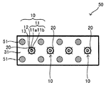
- FIG. 3 is a diagram illustrating a composite particle dispersion 50.
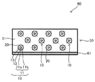
- FIG. 4 is a diagram illustrating a composite particle dispersion 60.
- FIG. 1 is a diagram illustrating a photovoltaic device 100.
- FIG. It is a figure explaining the photovoltaic apparatus.
- rare earth ions have a low light absorption probability, even if energy is given to the activator in the light state, the energy is hardly absorbed by the activator.
- the distance between the quantum dot and the activator is 10 nm or less, energy is easily transferred directly from the quantum dot to the activator by the dipole-dipole interaction. Since this dipole-dipole interaction is inversely proportional to the sixth power of the distance, the energy transfer probability suddenly increases as they approach each other. Therefore, in order to increase the up-conversion efficiency in the activator, it is effective to arrange the quantum dots and the activator so that the distance between the quantum dots and the activator is 10 nm or less.
- ⁇ Ln is the lifetime of the electrons excited by the activator
- N Ln is the number of activators existing in the vicinity of one quantum dot
- the quantum dot emits light.
- the quantum dot volume is V QD
- the photon flow from sunlight per unit area and unit time is N photon
- the quantum dot light absorption coefficient is ⁇ QD
- the quantum dot photoluminescence emission quantum yield is ⁇ PL
- ⁇ Ln >> N Ln / (V QD ⁇ N photon ⁇ ⁇ QD ⁇ ⁇ PL ) (3)
- the quantum dot has a large light absorption coefficient and that the volume (number of moles) of the quantum dot is large. It can be said that it is necessary to control and suppress so as not to increase too much.
- the upconversion intensity I UC defined by the ratio of the excitation light intensity to the incident light intensity is a power of the incident light intensity (nth power: n>) when the incident light intensity I in is weak in most rare earth phosphors. Proportional to 2).
- nth power n>
- the energy absorbed by the quantum dot according to the incident light intensity I in is present around the quantum dot.
- the energy transfer for each activator is inversely proportional to the number of activators. Therefore, the following formula (4) is established.
- the light absorption layer absorbs the light (excitation light) generated by up-conversion and only wants to increase the likelihood of up-conversion (up-conversion efficiency) when obtaining a UC type solar cell with improved power generation efficiency. It is also important to increase the intensity of the excitation light. This can also be achieved by collecting sunlight.
- FIG. 1 is a cross-sectional view illustrating a composite particle 10 of the present invention.
- a composite particle 10 shown in FIG. 1 includes a core part 11, a semiconductor part 12 that covers the surface of the core part 11, and a shell part 13 that covers the surface of the semiconductor part 12.
- the core part 11, the semiconductor The part 12 and the shell part 13 are arranged concentrically.
- the core part 11 has rare earth ions (activators 11a, 11a,...) Having an up-conversion effect and a holding agent 11b that holds the activators 11a, 11a,.
- the holding agent 11b is a semiconductor, and its band gap Eg11 is wider than the energy difference between the second excited state and the ground state of the activators 11a, 11a,.
- the diameter of the core part 11 is about 5 nm or less.
- the semiconductor portion 12 is a portion corresponding to a conventional quantum dot and includes a semiconductor.
- the semiconductor band gap Eg12 of the semiconductor portion 12 is narrower than the energy difference between the first excited state and the ground state of the activators 11a, 11a,..., And is discrete on the conduction band side and valence band side of the semiconductor. Quantum levels are formed.
- the semiconductor unit 12 can absorb light having energy greater than or equal to the band gap Eg12, and among the quantum levels formed on the conduction band side, the quantum level located closest to the conduction band end side and The energy difference Egq12 from the quantum level located closest to the valence band edge among the quantum levels formed on the valence band side becomes energy that can be absorbed by the activators 11a, 11a,.
- the thickness of the semiconductor portion 12 is less than 10 nm.
- the quantum level located closest to the conduction band edge among the quantum levels formed on the conduction band side may be referred to as “first quantum level on the conduction band side”.
- the quantum level located closest to the valence band end may be referred to as the “first quantum level on the valence band side”.
- the shell portion 13 is made of a semiconductor, and the band gap Eg13 of this semiconductor is wider than Egq12. In the composite particle 10, the thickness of the shell portion 13 is set to several nm or less.
- FIG. 2 is a diagram for explaining the energy transfer mode in the composite particle 10. 2, the same reference numerals as those used in FIG. 1 are attached to portions corresponding to the configuration shown in FIG. 1, and the description thereof is omitted as appropriate.
- ⁇ represents an electron
- ⁇ represents a hole
- a straight dashed arrow represents an energy transfer from the semiconductor portion 12 to the activator 11a.
- the semiconductor unit 12 can absorb light having energy of Egq12 or more. For example, when light whose energy is Egq12 is absorbed by the semiconductor unit 12, electrons are excited from the valence band of the semiconductor included in the semiconductor unit 12 so that the electrons exist in the first quantum level on the conduction band side. And holes are present in the first quantum level on the valence band side.
- the core part 11 exists inside the semiconductor part 12, and this core part 11 contains activators 11a, 11a,. Since the thickness of the semiconductor portion 12 is less than 10 nm and the diameter of the core portion 11 is about 5 nm or less, a site where electrons excited by absorbing light in the semiconductor portion 12 are present, and the activator 11a. The distance between and can be less than 10 nm. By causing the semiconductor of the semiconductor part 12 and the activator 11a to exist at such a distance, the energy of the semiconductor of the semiconductor part 12 is transferred to the activator 11a by dipole-dipole interaction. Is possible. As described above, Egq12 is adjusted so that the activator 11a can absorb energy.
- the energy absorbed by the semiconductor unit 12 can be absorbed by the activator 11a by being moved by the dipole-dipole interaction. In this way, when the activator 11a absorbs energy, electrons transition from the ground state of the activator 11a to the first excited state. On the other hand, in the semiconductor of the semiconductor unit 12 that has passed energy to the activator 11a, the electrons present in the first quantum level on the conduction band side lose energy.
- the energy absorbed by the semiconductor part 12 is transferred to the activator 11a, 11a,.
- the activators 11a, 11a,... Exist in the vicinity of the semiconductor of the semiconductor part 12, energy can be easily transferred from the semiconductor part 12 to the activators 11a, 11a,. Therefore, the activators 11a, 11a,... easily absorb the next energy while electrons that have transitioned from the ground state to the first excited state are present.
- the activators 11a, 11a,... Having the electrons transitioned to the first excited state absorb energy, the electrons existing in the first excited state can be further transitioned to the higher energy second excited state. Is possible.
- the electrons that have transitioned to the second excited state can emit light (excitation light) corresponding to the energy difference between the second excited state and the ground state when directly returning to the ground state.
- up-conversion is caused by the activators 11a, 11a,.
- the composite particle 10 is making the core part 11 which has activator 11a, 11a, ... and the semiconductor part 12 which has a semiconductor contact, the semiconductor of the semiconductor part 12 and activator 11a, 11a, ... are adjoining. Can be arranged. Further, by adjusting the diameter of the core portion 11 and the thickness of the semiconductor portion 12, the semiconductor of the semiconductor portion 12 and the activators 11a, 11a,... Can be moved to a distance at which energy can be transferred by dipole-dipole interaction. Can be arranged. When the light absorbed by the quantum dots is converted into light having other energy and emitted as in the prior art, the rare earth ions have a low light absorption probability, so it is difficult to improve the upconversion efficiency. On the other hand, according to the composite particle 10 that transfers energy by dipole-dipole interaction, the activators 11a, 11a,... It becomes easy.
- the semiconductor part 12 is arranged so as to cover the surface of the core part 11 having the activators 11a, 11a,.
- the semiconductor part 12 is arranged so as to cover the surface of the core part 11 having the activators 11a, 11a,.
- By suppressing the amount of activators 11a, 11a,... It is possible to increase the frequency of energy transfer from the semiconductor portion 12 toward the respective activators 11a, 11a,. It becomes easy for the activators 11a, 11a,... Having the transitioned electrons to absorb energy, and as a result, the upconversion efficiency can be increased.
- the thickness of the layer containing the activator is increased. Needs to be extremely thin. If a layer containing an activator having a very thin thickness is formed on the surface of the semiconductor, the activator in the vicinity of the surface tends to lose energy, so that up-conversion is unlikely to occur. Therefore, it is preferable to arrange the semiconductor part 12 so as to cover the surface of the core part 11 having the activators 11a, 11a,...
- the semiconductor portion 12 by arranging the semiconductor portion 12 so as to surround the core portion 11 having the activators 11a, 11a,..., The activators 11a, 11a,.
- the dipole dipole can be obtained from the semiconductor existing around the activators 11a, 11a,.
- the energy can be transferred to the activators 11a, 11a,. That is, in the composite particle 10, it is possible to collect energy absorbed by the semiconductor of the semiconductor portion 12 disposed around the activator 11a, 11a,... Disposed inside the semiconductor.
- a known rare earth ion having an up-conversion effect can be used as the activator 11a.
- examples of such rare earth include one or more selected from the group consisting of Er, Tm, Dy, and Eu.
- a known semiconductor having a wider band gap than the energy difference between the second excited state and the ground state of the activator 11a is appropriately used as the holding agent 11b that holds the activator 11a, 11a,. be able to.
- semiconductors include oxides such as Y 2 O 3 , YAlO 3 , and YAG, fluorides such as NaYF 4 , nitrides such as AlN, GaN, and SiAlON, and ZnS, ZnMgS, etc. when Yb is not included. Examples of such sulfides can be given.
- an insulating material can also be used as the core portion retention agent.
- the number of moles of the activator 11a dispersed in the holding agent 11b is not particularly limited. However, it is preferable to reduce the number of moles of the activator 11a from the viewpoint of easily increasing the upconversion efficiency and from the viewpoint of easily increasing the upconversion intensity. More specifically, when the number of moles of the activator 11a is X and the number of moles of the semiconductor used for the semiconductor portion 12 is Y, it is preferable that X / Y ⁇ 1/100.
- the manufacturing method of the core part 11 is not specifically limited,
- the core part 11 can be manufactured using the manufacturing method of a well-known quantum dot.
- a hot injection method, coprecipitation method, thermal decomposition, which are known techniques are performed using a raw material solution in which activators 11a, 11a,... Are dispersed in a liquid holding agent 11b.
- the core part 11 can be produced by a method, a solvothermal method, a sol-gel method, or the like.
- the core portion 11 further includes a rare earth ion (hereinafter referred to as "the energy transfer from the semiconductor portion 12 to the activators 11a, 11a, !). May be referred to as a “sensitizer”. Examples of the rare earth that can be used as the sensitizer include Yb.
- the semiconductor of the semiconductor part 12 can use suitably the well-known semiconductor whose band gap is less than the energy difference of the 1st excitation state of the activator 11a, and a ground state.
- semiconductors include CdSe, PbS, and InN, as well as chalcopyrite semiconductors typified by Cu 2 SnS 3 and the like.
- the semiconductor part 12 can be manufactured by the same method as the core part 11. If the core part 11 is produced by the above method, the core part 11 is separated from the liquid. Next, the separated core part 11 is put into a fluidized semiconductor (semiconductor to constitute the semiconductor part 12). Thus, when the core part 11 is put into the fluidized semiconductor, the semiconductor part 12 is formed on the surface of the core part 11 by a hot injection method, a coprecipitation method, a thermal decomposition method, a solvothermal method, a sol-gel method, or the like. Can do.
- the semiconductor part 12 can further contain a sensitizer similar to the sensitizer that can be contained in the core part 11. Even if the same sensitizer is dispersed in the core part 11 and the semiconductor part 12, for example, Yb is not easily affected by the crystal field, and a large difference in energy level occurs between Yb of the core part 11 and Yb of the semiconductor part 12. Therefore, energy can be quickly transferred from the semiconductor portion 12 to the activators 11a, 11a,.
- a known semiconductor having a wider band gap than Egq 12 can be used as the shell portion 13 as appropriate.
- a semiconductor having a wider band gap than Egq 12 can be used as the shell portion 13 as appropriate.
- examples of such a semiconductor include ZnO, ZnS, Y 2 O 3 , NaYF 4 and the like.
- an insulating material can be used for the shell portion.
- the shell part 13 can be manufactured by the same method as the core part 11 and the semiconductor part 12.
- the semiconductor portion 12 including the core portion 11 (hereinafter, simply referred to as “semiconductor portion 12”) is separated from the fluid.
- the separated semiconductor part 12 is placed in a fluidized semiconductor (semiconductor to form the shell part 13) or an insulating material.
- the shell part 13 is formed on the surface of the semiconductor part 12 by a hot injection method, a coprecipitation method, a thermal decomposition method, a solvothermal method, a sol-gel method, or the like. Can be produced.
- the intensity of the excitation light can be confirmed during the production of the semiconductor portion 12. This makes it possible to specify the thickness of the semiconductor part 12 where the intensity of the excitation light is increased. By determining the thickness of the semiconductor part 12 while checking the intensity of the excitation light, it becomes possible to match the energy Egq12 of the semiconductor part 12 with the absorbed energy of the activators 11a, 11a,. Increases efficiency and upconversion intensity.
- the composite particle 10 having the form in which the shell part 13 is disposed outside the semiconductor part 12 is illustrated, but the composite particle of the present invention is not limited to this form.
- the composite particles of the present invention may be in a form that does not have a shell portion, depending on the semiconductor material constituting the semiconductor portion 12. This is because depending on the semiconductor material constituting the semiconductor portion 12, the surrounding medium (for example, the support agent when the composite particles of the present invention are dispersed in the support agent) serves as the shell portion. That is, it is possible to play the role of preventing electrons from moving outward and the role of reducing defects on the surface that is the non-radiative recombination center of electrons and holes.
- FIG. 3 is a diagram illustrating the composite particle dispersion 30 of the present invention. 3, the same reference numerals as those used in FIG. 1 are attached to the same configuration as the composite particle 10 shown in FIG. 1, and the description thereof will be omitted as appropriate. 3, the composite particles 10, 10,... Are shown in a simplified manner.
- the composite particle dispersion 30 shown in FIG. 3 includes composite particles 10, 10,... And a support 31 that disperses these composite particles 10, 10,. Are modified with ligands 20, 20,.
- the support 31 is a transparent resin capable of transmitting light, and the ligand 20 is preferably an amine organic material having an amino group.
- the composite particles 10, 10,... With the ligands 20, 20,... Modified on the surface can be dispersed in a transparent resin in a fluid state. That is, the composite particle dispersion 30 is produced through a process in which the composite particles 10, 10,... Whose surfaces are modified with the ligands 20, 20,. Has been.
- the composite particles 10, 10,... Can increase the upconversion efficiency and increase the upconversion intensity as compared with a substance using a conventional rare earth phosphor. Therefore, by adopting the form shown in FIG. 3, it is possible to provide the composite particle dispersion 30 that can increase the upconversion efficiency and increase the upconversion intensity.
- examples of the amine-based organic substance having an amino group used for the ligand 20 that modifies the surface of the composite particles 10, 10,... include dodecylamine, hexadecylamine, octylamine, and the like. it can.
- a thiol-based organic substance such as dodecanethiol, hexadecanethiol, and benzenethiol can be used as a ligand for modifying the surface of the composite particle dispersed in the transparent resin. .
- a known transparent resin capable of allowing light to reach the composite particles 10, 10,. examples include polystyrene and acrylic resin.
- the support 31 for dispersing the composite particles 10 a mode in which a transparent resin is used as the support 31 for dispersing the composite particles 10, 10.
- the body is not limited to this form.
- the support for dispersing the composite particles may be a polar solvent such as water or a nonpolar solvent such as toluene or chloroform.
- the ligand for modifying the surface of the composite particles of the present invention includes, for example, a thiol group or an amine group coordinated to the particle surface, and On the opposite side, thioglycolic acid or ethanolamine having an acetic acid group or a hydroxyl group having high affinity with a polar solvent can be used.
- examples of the ligand that modifies the surface of the composite particles of the present invention include thiol groups and amine groups coordinated on the particle surface.
- dodecanethiol, hexadecanethiol, benzenethiol and the like having an acetic acid group and a hydrocarbon group having a high affinity with a nonpolar solvent on the opposite side can be used.
- FIG. 4 is a diagram for explaining the composite particle dispersion 40 of the present invention. 4, the same reference numerals as those used in FIG. 3 are given to the same configurations as those of the composite particle dispersion 30 shown in FIG. 3, and the description thereof will be omitted as appropriate.
- the composite particle dispersion 40 shown in FIG. 4 includes composite particles 10, 10,... Modified with ligands 20, 20,. Quantum dots 41, 41,... Modified with 20,.
- the quantum dot 41 is configured in the same manner as the composite particle 10 except that it does not have the core portion 11.
- quantum dots 41, 41,... are dispersed around the composite particle 10. By arranging the quantum dots 41, 41,... In the vicinity of the composite particle 10 (for example, a distance of about 10 nm or less), the energy absorbed by the quantum dots 41, 41,. It becomes possible to move to the composite particle 10.
- the quantum dots 41, 41,... are arranged so that the distance between the composite particle 10 and the quantum dots 41, 41,...
- the particles 10 can be absorbed.
- the energy absorbed by the quantum dots 41, 41,... Can be concentrated on the semiconductor portion 12 of the composite particle 10, and the energy that can be absorbed by the semiconductor portion 12 can be increased. become.
- the composite particle dispersion 40 in which the quantum dots 41, 41,... Are dispersed together with the composite particles 10, 10,..., It is possible to increase the upconversion intensity in each of the composite particles 10, 10,. Become.
- the quantum dots 41, 41,... Can be dispersed at a high concentration even in a liquid, the same effect as the composite particle dispersion 40 can be expected even when a liquid is used as a support.
- the upper limit concentration of the quantum dots 41, 41,... That can be dispersed in the liquid tends to be lower than the upper limit concentration of the quantum dots 41, 41,. Therefore, together with the composite particles of the present invention, in the case of a composite particle dispersion in which quantum dots configured in the same manner as the composite particles of the present invention except that they do not have a core portion are dispersed in a support, It is preferable to use a transparent resin.
- a sensitizer can be added to the quantum dots 41, 41,.
- a sensitizer can be added to the quantum dots 41, 41,.
- the quantum dots 41, 41,... And the composite particles 10, 10... The inside of the quantum dots 41, between the quantum dots 41 and the composite particles 10, and Since energy easily moves inside the composite particle 10, it is easy to increase the upconversion intensity.
- FIG. 5 is a diagram for explaining the composite particle dispersion 50 of the present invention.
- the same components as those of the composite particle dispersion 40 shown in FIG. 4 are denoted by the same reference numerals as those used in FIG.
- the composite particle dispersion 50 shown in FIG. 5 is the same as the composite particle dispersion 40 except that the metal fine particles 51, 51,... Are dispersed in the support 31 instead of the quantum dots 41, 41,.
- the configuration is the same as that of the particle dispersion 40. That is, in the composite particle dispersion 50, metal fine particles 51, 51,... Are dispersed around the composite particle 10.
- the metal fine particles 51 made of gold or silver having a diameter of several nanometers or more and several tens of nanometers or less (for example, a region having a distance of about 100 nm or less from the metal fine particles 51) Strength increases. Therefore, the composite particles 10, 10,... And the metal fine particles 51, 51,...
- the composite particle dispersion of the present invention using the metal fine particles 51, 51,..., The form using the metal fine particles 51, 51,.
- the particle dispersion is not limited to this form.
- the composite particle dispersion of the present invention is obtained by dispersing, in a support, the composite particles of the present invention, quantum dots that have the same structure as the composite particles of the present invention except that they do not have a core portion, and metal fine particles. It is also possible to adopt a different form. Even in such a form, it is possible to provide a composite particle dispersion with increased upconversion strength.
- FIG. 6 is a diagram for explaining the composite particle dispersion 60 of the present invention.
- the same components as those of the composite particle dispersion 30 shown in FIG. 3 are denoted by the same reference numerals as those used in FIG.
- the composite particle dispersion 60 shown in FIG. 6 has the composite particle dispersion 30 and a metal material 61 arranged so as to contact the support 31.
- the composite particles 10, 10, 10, 10, 10, 10, 10, 10, 10, 10, 10 10, 10 10 10 10 It is possible to increase the intensity of light absorbed by the semiconductor portions 12, 12,. In this way, by increasing the intensity of the light absorbed by the semiconductor part 12, it becomes possible to increase the intensity of the energy transferred to the core part 11, so the upconversion intensity by the activators 11a, 11a,. Can be increased. Therefore, according to the composite particle dispersion 60 having the metal material 61 arranged so as to be in contact with the support 31, the upconversion strength in the composite particles 10, 10,. It becomes possible.
- the form in which the composite particle dispersion 30 is used together with the metal material 61 is exemplified, but the metal material 61 is disposed so as to contact the support.
- the composite particle dispersion of the present invention is not limited to this form.
- the composite particle dispersion used together with the metal material may be the composite particle dispersion 40 or the composite particle dispersion 50 described above, except that the composite particle of the present invention and the core portion are not included. It may be a composite particle dispersion in which quantum dots configured in the same manner as the composite particles of the invention and metal fine particles are dispersed in a support. Even if the composite particle dispersion of these forms is used together with a metal material, it is possible to increase the up-conversion strength in the composite particles existing in the vicinity of the metal material.
- FIG. 7 is a diagram illustrating the photovoltaic device 100 of the present invention.
- the same components as those of the composite particle dispersion 30 shown in FIG. 3 are denoted by the same reference numerals as those used in FIG.
- the upper side of the drawing is the upstream side in the traveling direction of the incident light.
- the photovoltaic device 100 shown in FIG. 7 includes a first electrode 101, a photoelectric conversion unit 102, a second electrode 103, a transparent resin layer 104, a transparent glass layer 105, and a composite particle dispersion in order from the upstream side in the light traveling direction. 30 and a light reflecting portion 106.
- the first electrode 101 and the second electrode 103 that are in contact with the photoelectric conversion unit 102 are electrodes formed in a comb shape for the purpose of allowing light to enter the photoelectric conversion unit 102 and the composite particle dispersion 30, It is comprised with the well-known electroconductive material.
- the photoelectric conversion unit 102 includes an n layer 102a, an i layer 102b, and a p layer 102c in order from the top, and the electric power generated by absorbing light in these layers is the first electrode 101 or the second layer. It is taken out through the electrode 103.
- the transparent resin layer 104 is a layer provided to reduce unevenness formed on the surface of the p layer 102c on the composite particle dispersion 30 side by disposing the second electrode 103.
- the composite particle dispersion 30 The transparent glass layer 105 arranged on the upper surface side of the first electrode, the p layer 102c, and the second electrode 103 are connected via the transparent resin layer 104.
- the transparent glass layer 105 is used to (1) increase the mechanical strength, (2) as a substrate when manufacturing a battery disposed on the upper surface side, or (3) a substrate when forming the composite particle dispersion 30
- the composite particle dispersion 30 and the reflecting portion 106 that reflects light traveling from the upper side to the lower side of the paper toward the upper side of the paper surface are provided below the transparent glass layer 105. It has been.
- the composite particle dispersion 30 has improved up-conversion efficiency, and can generate light of energy that can be used from incident low-energy light to photoelectric conversion in the photoelectric conversion unit 102. .
- the light generated by the composite particle dispersion 30 travels in all directions. Of the light generated by the composite particle dispersion 30, the light traveling upward in the drawing passes through the transparent glass layer 105 and the transparent resin layer 104 and enters the photoelectric conversion unit 102, whereby the photoelectric conversion unit 102 Used for photoelectric conversion. On the other hand, the light traveling downward on the paper surface is reflected upward by the light reflecting unit 106 and passes through the composite particle dispersion 30, the transparent glass layer 105, and the transparent resin layer 104, and the photoelectric conversion unit. Incident light 102 is used for photoelectric conversion in the photoelectric conversion unit 102.
- the photovoltaic device 100 including the composite particle dispersion 30 According to the photovoltaic device 100 including the composite particle dispersion 30, light in a band that is not originally used for photoelectric conversion by the photoelectric conversion unit 102 is converted by the photoelectric conversion unit 102 using the composite particle dispersion 30. The light is converted into light having a usable bandwidth, and the converted light is incident on the photoelectric conversion unit 102 to be converted into electric power. As described above, the composite particle dispersion 30 can increase light in a band that can be used for photoelectric conversion. Therefore, according to the photovoltaic device 100, it is possible to increase power generation efficiency.
- the photoelectric conversion unit 102 may be a double-sided light receiving type in order to absorb not only light incident from the upper side of the paper but also light incident from the composite particle dispersion 30 side. is necessary.
- a photoelectric conversion part 102 can be comprised with the well-known substance which can be converted into electric power by absorbing the light produced
- FIG. In the photoelectric conversion unit 102 for example, single-crystal Si, amorphous Si, CIGS, organic solar cell, dye-sensitized solar cell, compound solar cell, etc.
- An electromotive device can be used as appropriate.
- the composite particle dispersion 30 may be formed on the transparent glass layer 105, and a battery may be attached to the opposite side. In the case of forming on the latter glass, the transparent glass layer The composite particle dispersion 30 may be formed on the opposite side of 105.
- the photovoltaic device 100 it is preferable to use a semiconductor material having a band gap energy of about 1.5 eV or more and 2.4 eV or less for the photoelectric conversion unit 102 from the viewpoint of easily increasing the power generation efficiency.
- the photoelectric conversion unit 102 configured as described above can be manufactured by a known method.
- the transparent resin layer 104 a known transparent resin that can be used for a solar cell and can adhere the p layer 102c and the second electrode 103 to the transparent glass layer 105 can be appropriately used.
- transparent resin include polyvinyl alcohol (PVA), polystyrene, acrylic resin, and the like.
- the transparent glass layer 105 a known transparent glass that can be used for solar cells can be used as appropriate.
- the light reflecting portion 106 a known reflecting material that can reflect the light incident from the composite particle dispersion 30 side to the composite particle dispersion 30 side can be appropriately used.
- the light reflection part 106 can be comprised with a well-known material, and a shape is not specifically limited, either.
- FIG. 8 is a diagram illustrating the photovoltaic device 200 of the present invention.
- the same components as those of the photovoltaic device 100 shown in FIG. 7 are denoted by the same reference symbols as used in FIG.
- the upper side of the drawing is the upstream side in the traveling direction of incident light.
- the metal material 61 of the composite particle dispersion 60 has a function of reflecting light traveling from the upper side to the lower side on the paper surface, like the light reflecting section 106 in the photovoltaic device 100. Therefore, the light that travels to the lower side of the paper among the light generated by the composite particle dispersion 60 can be incident on the photoelectric conversion unit 102 by being reflected by the metal material 61. It can be converted into electric power.
- the composite particle dispersion 60 is provided with the metal material 61, it is possible to increase the upconversion intensity in the composite particles 10, 10,... By the effect of surface plasmon resonance. That is, according to the photovoltaic device 200, light with increased intensity can be generated from the composite particle dispersion 60, and this light can be incident on the photoelectric conversion unit 102. Since the conversion efficiency can be increased by increasing the intensity of the incident light, according to the photovoltaic device 200, the conversion efficiency can be easily increased.
- SYMBOLS 10 Composite particle 11 ... Core part 11a ... Activator (rare earth ion which has an up-conversion effect) 11b ... Retaining agent 12 ... Semiconductor part 13 ... Shell part 20 ... Ligand 30, 40, 50, 60 ... Composite particle dispersion (wavelength conversion part) DESCRIPTION OF SYMBOLS 31 ... Support agent 41 ... Quantum dot 51 ... Metal fine particle 61 ... Metal material 100, 200 ... Photovoltaic device 101 ... 1st electrode 102 ... Photoelectric conversion part 102a ... n layer 102b ... i layer 102c ... p layer 103 ... 2nd Electrode 104 ... Transparent resin layer 105 ... Transparent glass layer 106 ... Light reflecting portion
Landscapes
- Photovoltaic Devices (AREA)
- Luminescent Compositions (AREA)
Abstract
Description
本発明の第1の態様は、アップコンバージョン効果を有する希土類イオン及び該希土類イオンを保持する保持剤を有するコア部と、該コア部の一部又は全部を覆う半導体部と、を有し、上記保持剤は、上記希土類イオンで二段階目の励起を生じさせるために必要なエネルギー差よりもバンドギャップが広い半導体、又は、絶縁体によって構成され、上記半導体部は、バンドギャップが、上記希土類イオンの第1励起状態と基底状態とのエネルギー差未満である半導体を有している、複合粒子である。
τLn/NLn>>ΔtQD …式(1)
なお、量子ドットにおけるアップコンバージョンで生成される光子数を量子ドットに入射した光子数で割ることによって得られる量子収率ΦUCで、ΔtQDを割ると、ほぼ、量子ドットがエネルギーを放出する平均時間間隔になる。
ΔtQD≒1/(VQD・Nphoton・αQD・ΦPL) …式(2)
が成り立つので、上記式(1)及び上記式(2)から、下記式(3)が導かれる。
τLn>>NLn/(VQD・Nphoton・αQD・ΦPL) …式(3)
IUC∝NLn×(Iin)n∝NLn×(1/NLn)n=NLn (1-n) …式(4)
以下、図面を参照しつつ、本発明の実施の形態について説明する。以下の図面では、繰り返される符号の一部を省略することがある。なお、以下に示す形態は本発明の例示であり、本発明は以下に示す形態に限定されない。
図1は、本発明の複合粒子10を説明する断面図である。図1に示した複合粒子10は、コア部11と、このコア部11の表面を覆う半導体部12と、この半導体部12の表面を覆うシェル部13と、を有し、コア部11、半導体部12、及び、シェル部13が同心円状に配置されている。
図3は、本発明の複合粒子分散体30を説明する図である。図3において、図1に示した複合粒子10と同様の構成には、図1で使用した符号と同一の符号を付し、その説明を適宜省略する。図3では、複合粒子10、10、…を簡略化して示している。
図7は、本発明の光起電装置100を説明する図である。図7において、図3に示した複合粒子分散体30と同様の構成には、図3で使用した符号と同一の符号を付し、その説明を適宜省略する。図7では、紙面上側が入射光の進行方向上流側である。
11…コア部
11a…賦活剤(アップコンバージョン効果を有する希土類イオン)
11b…保持剤
12…半導体部
13…シェル部
20…配位子
30、40、50、60…複合粒子分散体(波長変換部)
31…支持剤
41…量子ドット
51…金属微粒子
61…金属材
100、200…光起電装置
101…第1電極
102…光電変換部
102a…n層
102b…i層
102c…p層
103…第2電極
104…透明樹脂層
105…透明ガラス層
106…光反射部
Claims (11)
- アップコンバージョン効果を有する希土類イオン及び該希土類イオンを保持する保持剤を有するコア部と、該コア部の一部又は全部を覆う半導体部と、を有し、
前記保持剤は、前記希土類イオンで二段階目の励起を生じさせるために必要なエネルギー差よりもバンドギャップが広い半導体、又は、絶縁体によって構成され、
前記半導体部は、バンドギャップが、前記希土類イオンの第1励起状態と基底状態とのエネルギー差未満である半導体を有している、複合粒子。 - 前記半導体部に含まれている前記半導体のバンドギャップよりもバンドギャップが広い半導体、又は、絶縁体によって、前記半導体部の一部又は全部が覆われている、請求項1に記載の複合粒子。
- 前記コア部に含まれている前記希土類イオンのモル数をX、前記半導体部に含まれている前記半導体のモル数をY、とするとき、X/Y≦1/100である、請求項1又は2に記載の複合粒子。
- 前記コア部に含まれている前記希土類イオンがErイオンである、請求項1~3のいずれか1項に記載の複合粒子。
- 前記コア部、及び/又は、前記半導体部に、Ybイオンが含有されている、請求項4に記載の複合粒子。
- 支持剤と、該支持剤内に分散されて支持される複合粒子と、を有し、
前記複合粒子が、表面が配位子で修飾されている請求項1~5のいずれか1項に記載の複合粒子である、複合粒子分散体。 - 前記支持剤に、さらに、アップコンバージョン効果を有する前記希土類イオンを含有していない量子ドットが分散されている、請求項6に記載の複合粒子分散体。
- 前記支持剤に、さらに、金属微粒子が分散されている、請求項6又は7に記載の複合粒子分散体。
- 前記支持剤の表面に、金属が接触している、請求項6~8のいずれか1項に記載の複合粒子分散体。
- 光の進行方向上流側から順に、光エネルギーを電力に変換する光電変換部と、波長変換部と、光反射部と、が配置され、
前記波長変換部に、請求項6~8のいずれか1項に記載の複合粒子分散体が用いられている、光起電装置。 - 光の進行方向上流側から順に、光エネルギーを電力に変換する光電変換部と、波長変換部と、が配置され、
前記波長変換部に、請求項9に記載の複合粒子分散体が用いられ、且つ、前記金属と前記光電変換部との間に前記支持剤が配置されている、光起電装置。
Priority Applications (4)
| Application Number | Priority Date | Filing Date | Title |
|---|---|---|---|
| US14/413,534 US9306090B2 (en) | 2012-07-23 | 2012-07-23 | Composite particle, composite particle dispersion, and photovoltaic device, |
| CN201280074101.2A CN104379698B (zh) | 2012-07-23 | 2012-07-23 | 复合粒子、复合粒子分散体及光伏装置 |
| PCT/JP2012/068630 WO2014016893A1 (ja) | 2012-07-23 | 2012-07-23 | 複合粒子、複合粒子分散体、及び、光起電装置 |
| JP2014526630A JP5783332B2 (ja) | 2012-07-23 | 2012-07-23 | 複合粒子、複合粒子分散体、及び、光起電装置 |
Applications Claiming Priority (1)
| Application Number | Priority Date | Filing Date | Title |
|---|---|---|---|
| PCT/JP2012/068630 WO2014016893A1 (ja) | 2012-07-23 | 2012-07-23 | 複合粒子、複合粒子分散体、及び、光起電装置 |
Publications (1)
| Publication Number | Publication Date |
|---|---|
| WO2014016893A1 true WO2014016893A1 (ja) | 2014-01-30 |
Family
ID=49996730
Family Applications (1)
| Application Number | Title | Priority Date | Filing Date |
|---|---|---|---|
| PCT/JP2012/068630 Ceased WO2014016893A1 (ja) | 2012-07-23 | 2012-07-23 | 複合粒子、複合粒子分散体、及び、光起電装置 |
Country Status (4)
| Country | Link |
|---|---|
| US (1) | US9306090B2 (ja) |
| JP (1) | JP5783332B2 (ja) |
| CN (1) | CN104379698B (ja) |
| WO (1) | WO2014016893A1 (ja) |
Cited By (8)
| Publication number | Priority date | Publication date | Assignee | Title |
|---|---|---|---|---|
| JP2015143289A (ja) * | 2014-01-31 | 2015-08-06 | 国立研究開発法人物質・材料研究機構 | 蛍光体、照明器具および画像表示装置 |
| JP2015191908A (ja) * | 2014-03-27 | 2015-11-02 | 京セラ株式会社 | 量子ドット,光電変換層,光電変換装置 |
| JP2016132685A (ja) * | 2015-01-15 | 2016-07-25 | 株式会社デンソー | 波長変換材料、受光システム、及び測距システム |
| JP2016225546A (ja) * | 2015-06-02 | 2016-12-28 | シャープ株式会社 | 光電変換素子 |
| WO2017204018A1 (ja) * | 2016-05-24 | 2017-11-30 | セイコーエプソン株式会社 | スタンプ用インクおよびスタンプ台 |
| JPWO2017130943A1 (ja) * | 2016-01-28 | 2018-02-01 | 積水化学工業株式会社 | ランタノイド含有無機材料微粒子、波長変換インク、塗工物及び判定装置 |
| JP2018087328A (ja) * | 2016-11-22 | 2018-06-07 | 積水化学工業株式会社 | ランタノイド含有無機材料微粒子 |
| KR20180072798A (ko) * | 2015-11-02 | 2018-06-29 | 나노코 테크놀로지스 리미티드 | 녹색-발광 양자점들 및 적색 ksf 형광체를 포함하는 디스플레이 장치 |
Families Citing this family (8)
| Publication number | Priority date | Publication date | Assignee | Title |
|---|---|---|---|---|
| US20150357496A1 (en) * | 2013-03-05 | 2015-12-10 | Sharp Kabushiki Kaisha | Core-shell particle, upconversion layer, and photoelectric conversion device |
| US8957490B2 (en) | 2013-06-28 | 2015-02-17 | Infineon Technologies Dresden Gmbh | Silicon light trap devices |
| DE102014102848B4 (de) * | 2013-12-19 | 2025-01-02 | Osram Gmbh | Konversionselement, Verfahren zur Herstellung eines Konversionselements, optoelektronisches Bauelement umfassend ein Konversionselement |
| US10266769B2 (en) * | 2014-04-08 | 2019-04-23 | Ns Materials Inc. | Quantum dot, manufacturing method of the dot, and compact, sheet member, wavelength conversion member and light emitting apparatus using the quantum dot |
| CN108269892B (zh) * | 2016-12-30 | 2021-06-22 | Tcl科技集团股份有限公司 | 具有量子阱能级结构的合金材料、制备方法及半导体器件 |
| WO2019246175A1 (en) * | 2018-06-19 | 2019-12-26 | Flux Photon Corporation | A broadband exciton scavenger device |
| US11211458B2 (en) * | 2018-06-19 | 2021-12-28 | Flux Photon Corporation | Photocatalytic device based on rare-earth elements: methods of manufacture and use |
| JP7117170B2 (ja) * | 2018-06-20 | 2022-08-12 | スタンレー電気株式会社 | 発光装置 |
Citations (3)
| Publication number | Priority date | Publication date | Assignee | Title |
|---|---|---|---|---|
| JP2011049207A (ja) * | 2009-08-25 | 2011-03-10 | Sumitomo Bakelite Co Ltd | 複合粒子、樹脂組成物、波長変換層および光起電装置 |
| JP2012001585A (ja) * | 2010-06-15 | 2012-01-05 | Sumitomo Bakelite Co Ltd | 複合粒子、組成物、波長変換層および光起電装置。 |
| JP2012023123A (ja) * | 2010-07-13 | 2012-02-02 | Sumitomo Bakelite Co Ltd | 複合粒子、組成物、波長変換層および光起電装置。 |
Family Cites Families (2)
| Publication number | Priority date | Publication date | Assignee | Title |
|---|---|---|---|---|
| US20140076404A1 (en) * | 2010-12-15 | 2014-03-20 | Mei-Chee Tan | Ir-activated photoelectric systems |
| CN102268259B (zh) * | 2011-06-14 | 2013-09-25 | 中国科学院长春光学精密机械与物理研究所 | 发光中心分区域掺杂稀土上转换荧光材料及其制备方法 |
-
2012
- 2012-07-23 US US14/413,534 patent/US9306090B2/en active Active
- 2012-07-23 JP JP2014526630A patent/JP5783332B2/ja active Active
- 2012-07-23 CN CN201280074101.2A patent/CN104379698B/zh active Active
- 2012-07-23 WO PCT/JP2012/068630 patent/WO2014016893A1/ja not_active Ceased
Patent Citations (3)
| Publication number | Priority date | Publication date | Assignee | Title |
|---|---|---|---|---|
| JP2011049207A (ja) * | 2009-08-25 | 2011-03-10 | Sumitomo Bakelite Co Ltd | 複合粒子、樹脂組成物、波長変換層および光起電装置 |
| JP2012001585A (ja) * | 2010-06-15 | 2012-01-05 | Sumitomo Bakelite Co Ltd | 複合粒子、組成物、波長変換層および光起電装置。 |
| JP2012023123A (ja) * | 2010-07-13 | 2012-02-02 | Sumitomo Bakelite Co Ltd | 複合粒子、組成物、波長変換層および光起電装置。 |
Cited By (11)
| Publication number | Priority date | Publication date | Assignee | Title |
|---|---|---|---|---|
| JP2015143289A (ja) * | 2014-01-31 | 2015-08-06 | 国立研究開発法人物質・材料研究機構 | 蛍光体、照明器具および画像表示装置 |
| JP2015191908A (ja) * | 2014-03-27 | 2015-11-02 | 京セラ株式会社 | 量子ドット,光電変換層,光電変換装置 |
| JP2016132685A (ja) * | 2015-01-15 | 2016-07-25 | 株式会社デンソー | 波長変換材料、受光システム、及び測距システム |
| JP2016225546A (ja) * | 2015-06-02 | 2016-12-28 | シャープ株式会社 | 光電変換素子 |
| KR20180072798A (ko) * | 2015-11-02 | 2018-06-29 | 나노코 테크놀로지스 리미티드 | 녹색-발광 양자점들 및 적색 ksf 형광체를 포함하는 디스플레이 장치 |
| KR102163254B1 (ko) | 2015-11-02 | 2020-10-08 | 나노코 테크놀로지스 리미티드 | 녹색-발광 양자점들 및 적색 ksf 형광체를 포함하는 디스플레이 장치 |
| JPWO2017130943A1 (ja) * | 2016-01-28 | 2018-02-01 | 積水化学工業株式会社 | ランタノイド含有無機材料微粒子、波長変換インク、塗工物及び判定装置 |
| US11274248B2 (en) | 2016-01-28 | 2022-03-15 | Sekisui Chemical Co., Ltd. | Lanthanoid-containing inorganic material microparticles, wavelength-converting ink, coated article, and determination apparatus |
| WO2017204018A1 (ja) * | 2016-05-24 | 2017-11-30 | セイコーエプソン株式会社 | スタンプ用インクおよびスタンプ台 |
| JPWO2017204018A1 (ja) * | 2016-05-24 | 2019-03-22 | セイコーエプソン株式会社 | スタンプ用インクおよびスタンプ台 |
| JP2018087328A (ja) * | 2016-11-22 | 2018-06-07 | 積水化学工業株式会社 | ランタノイド含有無機材料微粒子 |
Also Published As
| Publication number | Publication date |
|---|---|
| CN104379698A (zh) | 2015-02-25 |
| JPWO2014016893A1 (ja) | 2016-07-07 |
| CN104379698B (zh) | 2016-05-11 |
| US20150136229A1 (en) | 2015-05-21 |
| JP5783332B2 (ja) | 2015-09-24 |
| US9306090B2 (en) | 2016-04-05 |
Similar Documents
| Publication | Publication Date | Title |
|---|---|---|
| JP5783332B2 (ja) | 複合粒子、複合粒子分散体、及び、光起電装置 | |
| CN102246314B (zh) | 发光光伏发生器以及用在光伏发生器中的波导 | |
| Lutich et al. | Multiexcitonic dual emission in CdSe/CdS tetrapods and nanorods | |
| CN104115284B (zh) | 用于作物生长的发光的发电窗 | |
| ES2804756T3 (es) | Material compuesto y dispositivo de recolección de luz | |
| KR20110131212A (ko) | 비방사성 에너지 전환을 갖는 광학 소자 | |
| Wei et al. | Mn-doped multiple quantum well perovskites for efficient large-area luminescent solar concentrators | |
| US9373740B1 (en) | Wavelength converting structure for near-infrared rays and solar cell comprising the same | |
| KR20150090035A (ko) | 고변환 효율을 갖는 광발전 소자 | |
| KR101208272B1 (ko) | 양면 구조를 가지는 태양전지 및 이의 제조방법 | |
| KR101892637B1 (ko) | 태양전지 패널 및 그를 포함하는 창호 | |
| US8759666B2 (en) | Wavelength conversion photovoltaics | |
| US20090133750A1 (en) | Solar cell | |
| KR101333978B1 (ko) | 고상 발광 소자용 픽셀 구조 | |
| Van Sark et al. | Luminescent solar concentrators: The route to 10% efficiency | |
| KR102394750B1 (ko) | 태양광 집광 장치 및 이를 포함하는 태양전지 모듈 | |
| KR101765932B1 (ko) | 태양광 발전장치 | |
| US10510915B2 (en) | Porous silicon nanowire photovoltaic cell | |
| CN207691196U (zh) | 日盲紫外单光子源 | |
| KR101210007B1 (ko) | 태양광 발전장치 | |
| US20120222733A1 (en) | Organic photovoltaic cell structure | |
| CN117769277A (zh) | 一种增强电荷传输的三端叠层太阳电池 | |
| JP2015079870A (ja) | 太陽電池 |
Legal Events
| Date | Code | Title | Description |
|---|---|---|---|
| WWE | Wipo information: entry into national phase |
Ref document number: 201280074101.2 Country of ref document: CN |
|
| 121 | Ep: the epo has been informed by wipo that ep was designated in this application |
Ref document number: 12881745 Country of ref document: EP Kind code of ref document: A1 |
|
| ENP | Entry into the national phase |
Ref document number: 2014526630 Country of ref document: JP Kind code of ref document: A |
|
| NENP | Non-entry into the national phase |
Ref country code: DE |
|
| WWE | Wipo information: entry into national phase |
Ref document number: 14413534 Country of ref document: US |
|
| 122 | Ep: pct application non-entry in european phase |
Ref document number: 12881745 Country of ref document: EP Kind code of ref document: A1 |