WO2014010478A1 - 光源装置 - Google Patents
光源装置 Download PDFInfo
- Publication number
- WO2014010478A1 WO2014010478A1 PCT/JP2013/068214 JP2013068214W WO2014010478A1 WO 2014010478 A1 WO2014010478 A1 WO 2014010478A1 JP 2013068214 W JP2013068214 W JP 2013068214W WO 2014010478 A1 WO2014010478 A1 WO 2014010478A1
- Authority
- WO
- WIPO (PCT)
- Prior art keywords
- light
- wavelength conversion
- light source
- conversion element
- optical axis
- Prior art date
Links
Images

Classifications
-
- H—ELECTRICITY
- H01—ELECTRIC ELEMENTS
- H01S—DEVICES USING THE PROCESS OF LIGHT AMPLIFICATION BY STIMULATED EMISSION OF RADIATION [LASER] TO AMPLIFY OR GENERATE LIGHT; DEVICES USING STIMULATED EMISSION OF ELECTROMAGNETIC RADIATION IN WAVE RANGES OTHER THAN OPTICAL
- H01S5/00—Semiconductor lasers
- H01S5/005—Optical components external to the laser cavity, specially adapted therefor, e.g. for homogenisation or merging of the beams or for manipulating laser pulses, e.g. pulse shaping
- H01S5/0087—Optical components external to the laser cavity, specially adapted therefor, e.g. for homogenisation or merging of the beams or for manipulating laser pulses, e.g. pulse shaping for illuminating phosphorescent or fluorescent materials, e.g. using optical arrangements specifically adapted for guiding or shaping laser beams illuminating these materials
-
- F—MECHANICAL ENGINEERING; LIGHTING; HEATING; WEAPONS; BLASTING
- F21—LIGHTING
- F21V—FUNCTIONAL FEATURES OR DETAILS OF LIGHTING DEVICES OR SYSTEMS THEREOF; STRUCTURAL COMBINATIONS OF LIGHTING DEVICES WITH OTHER ARTICLES, NOT OTHERWISE PROVIDED FOR
- F21V13/00—Producing particular characteristics or distribution of the light emitted by means of a combination of elements specified in two or more of main groups F21V1/00 - F21V11/00
- F21V13/02—Combinations of only two kinds of elements
- F21V13/04—Combinations of only two kinds of elements the elements being reflectors and refractors
-
- G—PHYSICS
- G02—OPTICS
- G02B—OPTICAL ELEMENTS, SYSTEMS OR APPARATUS
- G02B19/00—Condensers, e.g. light collectors or similar non-imaging optics
- G02B19/0004—Condensers, e.g. light collectors or similar non-imaging optics characterised by the optical means employed
- G02B19/0028—Condensers, e.g. light collectors or similar non-imaging optics characterised by the optical means employed refractive and reflective surfaces, e.g. non-imaging catadioptric systems
-
- G—PHYSICS
- G02—OPTICS
- G02B—OPTICAL ELEMENTS, SYSTEMS OR APPARATUS
- G02B19/00—Condensers, e.g. light collectors or similar non-imaging optics
- G02B19/0033—Condensers, e.g. light collectors or similar non-imaging optics characterised by the use
- G02B19/0047—Condensers, e.g. light collectors or similar non-imaging optics characterised by the use for use with a light source
- G02B19/0061—Condensers, e.g. light collectors or similar non-imaging optics characterised by the use for use with a light source the light source comprising a LED
-
- G—PHYSICS
- G02—OPTICS
- G02B—OPTICAL ELEMENTS, SYSTEMS OR APPARATUS
- G02B26/00—Optical devices or arrangements for the control of light using movable or deformable optical elements
- G02B26/007—Optical devices or arrangements for the control of light using movable or deformable optical elements the movable or deformable optical element controlling the colour, i.e. a spectral characteristic, of the light
-
- G—PHYSICS
- G02—OPTICS
- G02B—OPTICAL ELEMENTS, SYSTEMS OR APPARATUS
- G02B27/00—Optical systems or apparatus not provided for by any of the groups G02B1/00 - G02B26/00, G02B30/00
- G02B27/10—Beam splitting or combining systems
- G02B27/14—Beam splitting or combining systems operating by reflection only
- G02B27/141—Beam splitting or combining systems operating by reflection only using dichroic mirrors
-
- H—ELECTRICITY
- H04—ELECTRIC COMMUNICATION TECHNIQUE
- H04N—PICTORIAL COMMUNICATION, e.g. TELEVISION
- H04N23/00—Cameras or camera modules comprising electronic image sensors; Control thereof
- H04N23/10—Cameras or camera modules comprising electronic image sensors; Control thereof for generating image signals from different wavelengths
- H04N23/12—Cameras or camera modules comprising electronic image sensors; Control thereof for generating image signals from different wavelengths with one sensor only
-
- G—PHYSICS
- G02—OPTICS
- G02B—OPTICAL ELEMENTS, SYSTEMS OR APPARATUS
- G02B2207/00—Coding scheme for general features or characteristics of optical elements and systems of subclass G02B, but not including elements and systems which would be classified in G02B6/00 and subgroups
- G02B2207/113—Fluorescence
-
- H—ELECTRICITY
- H01—ELECTRIC ELEMENTS
- H01S—DEVICES USING THE PROCESS OF LIGHT AMPLIFICATION BY STIMULATED EMISSION OF RADIATION [LASER] TO AMPLIFY OR GENERATE LIGHT; DEVICES USING STIMULATED EMISSION OF ELECTROMAGNETIC RADIATION IN WAVE RANGES OTHER THAN OPTICAL
- H01S5/00—Semiconductor lasers
- H01S5/005—Optical components external to the laser cavity, specially adapted therefor, e.g. for homogenisation or merging of the beams or for manipulating laser pulses, e.g. pulse shaping
- H01S5/0078—Optical components external to the laser cavity, specially adapted therefor, e.g. for homogenisation or merging of the beams or for manipulating laser pulses, e.g. pulse shaping for frequency filtering
-
- H—ELECTRICITY
- H01—ELECTRIC ELEMENTS
- H01S—DEVICES USING THE PROCESS OF LIGHT AMPLIFICATION BY STIMULATED EMISSION OF RADIATION [LASER] TO AMPLIFY OR GENERATE LIGHT; DEVICES USING STIMULATED EMISSION OF ELECTROMAGNETIC RADIATION IN WAVE RANGES OTHER THAN OPTICAL
- H01S5/00—Semiconductor lasers
- H01S5/30—Structure or shape of the active region; Materials used for the active region
- H01S5/32—Structure or shape of the active region; Materials used for the active region comprising PN junctions, e.g. hetero- or double- heterostructures
- H01S5/323—Structure or shape of the active region; Materials used for the active region comprising PN junctions, e.g. hetero- or double- heterostructures in AIIIBV compounds, e.g. AlGaAs-laser, InP-based laser
- H01S5/32308—Structure or shape of the active region; Materials used for the active region comprising PN junctions, e.g. hetero- or double- heterostructures in AIIIBV compounds, e.g. AlGaAs-laser, InP-based laser emitting light at a wavelength less than 900 nm
- H01S5/32341—Structure or shape of the active region; Materials used for the active region comprising PN junctions, e.g. hetero- or double- heterostructures in AIIIBV compounds, e.g. AlGaAs-laser, InP-based laser emitting light at a wavelength less than 900 nm blue laser based on GaN or GaP
Definitions
- the present invention relates to a light source device.
- Patent Document 1 a light source device that generates light of a plurality of colors using a light source that outputs light of a single color such as a semiconductor light source is known (see, for example, Patent Document 1).
- a blue laser diode (LD) is used as a light source, and a rotation having a region transmitting blue light and a region generating red and green fluorescence and reflecting these fluorescence by blue light A wheel is provided to guide blue light and red and green light in separate light paths.
- LD blue laser diode
- Patent No. 4711154 gazette
- the present invention has been made in view of the above-described circumstances, and an object of the present invention is to provide a light source device having a small optical path configuration and capable of generating light with high efficiency.
- the present invention comprises a light source for outputting monochromatic light, a wavelength conversion element disposed on an output optical axis of the light source and generating light of a color different from the monochromatic light by being irradiated with the monochromatic light, and
- the output optical axis is disposed between the light source and the wavelength conversion element, and transmits the monochromatic light and scatters the light generated in the wavelength conversion element toward the light source in the direction of the wavelength conversion element.
- a dichroic mirror that folds back in parallel to the light source device.
- monochromatic light output from the light source is converted to light of a different color in the wavelength conversion element, and then output along the output optical axis.
- part of the light scattered to the light source side is folded back only once in parallel with the output optical axis by a single dichroic mirror, and is scattered to the opposite side to the light source It is output together with other light. Therefore, in the light after conversion, the occurrence of the deviation of the optical axis and the loss is prevented.
- light can be generated and output with high efficiency from monochromatic light output from the light source.
- the wavelength conversion element, and the dichroic mirror are all arranged in a line on the output optical axis, the optical path configuration can be miniaturized.
- a first collimating optical system which is disposed between the dichroic mirror and the wavelength conversion element and collimates the light scattered from the wavelength conversion element toward the light source, and the wavelength conversion element
- a second collimating optical system may be provided which is disposed in the subsequent stage and collimates the light scattered from the wavelength conversion element to the side opposite to the light source. In this way, light generated in the wavelength conversion element and scattered in each direction can be converted into parallel light and output by the first collimating optical system and the second collimating optical system.
- the first collimating optical system may include a lens having a flat surface, and the dichroic mirror may be integrally formed on the flat surface.
- the plurality of wavelength conversion elements may be arranged in a direction along or crossing the output optical axis in the irradiation area of the monochromatic light on the output optical axis, and a plurality of sets of The wavelength conversion element and the dichroic mirror may be arranged in series on the output optical axis.
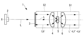
- the light source device 1 is, as shown in FIG. 1, a light source 2 for outputting monochromatic light, and an output optical axis X of the light source 2 (hereinafter, also simply referred to as an optical axis X) in line.
- the dichroic mirror 3, the first collimating optical system 4, the wavelength conversion element 5, and the second collimating optical system 6 are provided.
- the light source 2 is a semiconductor light source, a laser diode or the like that outputs monochromatic light with high directivity.
- blue laser light L having a wavelength of 450 nm is assumed as monochromatic light beam.
- a single light source 2 is shown in FIG. 1, a plurality of (for example, 2 ⁇ 2 or 3 ⁇ 3) light sources 2 outputting laser light L parallel to each other are arranged in an array. It may be
- the dichroic mirror 3 is disposed perpendicular to the optical axis X, and transmits the laser light L incident from the light source 2 along the optical axis X. Further, the dichroic mirror 3 reflects the fluorescence Lb 'back scattered in the wavelength conversion element 5 along the optical axis X as described later.
- the dichroic mirror 3 has a characteristic of transmitting light of a wavelength of 500 nm or less and reflecting light of a wavelength longer than 500 nm.
- FIG. 8 shows the relationship between the wavelength of the laser light L assumed in the present embodiment, the wavelength of the fluorescence L ′ generated by the wavelength conversion element 5 (described later), and the spectral transmission characteristics of the dichroic mirror 3.
- the left vertical axis is the light transmittance of the dichroic mirror 3, and the right vertical axis is the relative intensity of the laser light L and the fluorescence L '.
- the first collimating optical system 4 includes a meniscus lens or a plano-convex lens disposed with the convex surface facing the light source 2 side.
- the first collimating optical system 4 collimates the fluorescence L ′ backscattered by the wavelength conversion element 5 and emits the collimated fluorescence L ′ to the dichroic mirror 3. Further, the first collimating optical system 4 condenses the fluorescence L ′ reflected and returned by the dichroic mirror 3 on the wavelength conversion element 5.
- the occurrence of spherical aberration can be suppressed by arranging the meniscus lens or the plano-convex lens with the convex surface facing the light source 2 as described above.
- the first collimating optical system 4 is preferably composed of a plurality of lenses in which the above-described meniscus lens or plano-convex lens is combined with a lens (not shown). By doing so, the occurrence of spherical aberration can be further suppressed.
- the wavelength conversion element 5 is an element that emits light by being irradiated with the laser light L (monochromatic light) from the light source 2 and holds, for example, a phosphor or a quantum dot excited by the laser light L.
- the wavelength conversion element 5 is a phosphor that includes the wavelength 450 nm of the laser light L in the excitation wavelength band and generates fluorescence (light) L 'having a peak wavelength of 550 nm.
- the fluorescence L 'generated in the wavelength conversion element 5 is fluorescence Lf' which is forward scattered in the space S1 on the front side (the opposite side to the light source 2) of the optical axis X, and the rear side (the same side as the light source 2) It is divided into the fluorescent light Lb 'backscattered to space S2 of.
- the forward scattered fluorescence Lf ′ is incident on the second collimating optical system 6, and the backscattered fluorescence Lb ′ is incident on the first collimating optical system 4.
- the second collimating optical system 6 includes one meniscus lens or plano-convex lens disposed with the convex surface facing the optical axis X forward.
- the second collimating optical system 6 collimates the fluorescence L ′ incident from the wavelength conversion element 5 and emits it along the optical axis X.
- the second collimating optical system 6 is preferably composed of a plurality of lenses in which the above-described meniscus lens or plano-convex lens and a lens (not shown) are combined. By doing so, the occurrence of spherical aberration can be further suppressed.
- the blue laser light L output from the light source 2 transmits the dichroic mirror 3 and is incident on the wavelength conversion element 5 so that the green fluorescence in the wavelength conversion element 5 is generated.
- the fluorescence Lf ′ which is forward scattered is converted into parallel light by the second collimating optical system 6 and then output to the outside of the light source device 1 along the optical axis X.
- the fluorescence Lb ′ which has been backscattered and travels in the reverse direction to the optical axis X is converted into parallel light by the first collimating optical system 4 and then folded back by the dichroic mirror 3.
- the light is collected on the wavelength conversion element 5.
- the overlap between the light emission wavelength band of the wavelength conversion element 5 and the excitation wavelength band is small or not at all. Therefore, the fluorescence Lb ′ collected on the wavelength conversion element 5 excites the phosphor and hardly causes energy loss, and passes through the wavelength conversion element 5.
- the fluorescence Lb ′ transmitted through the wavelength conversion element 5 is converted into parallel light by the second collimating optical system 6 as with the forward-scattered fluorescence Lf ′ and then the outside of the light source device 1 along the optical axis X Output.
- the entire fluorescence L 'generated in the wavelength conversion element 5 is output from the light source device 1 as the final output light.
- an optical path is formed linearly along the output optical axis X of the light source 2, and the backscattered fluorescence Lb 'is a single dichroic disposed perpendicular to the optical axis X.
- the mirror 3 reflects light in a direction parallel to the optical axis X and only once. Therefore, the occurrence of optical axis misalignment and loss of the fluorescence Lb 'is prevented, and the reflected fluorescence Lb' is output along the optical axis X to the outside of the light source device 1 with sufficiently high efficiency.
- This has the advantage that the fluorescent light L 'as output light can be generated from the laser light L with high efficiency. Further, by making the optical path straight, there is an advantage that the optical path configuration can be made compact.
- the single wavelength conversion element 5 is provided to generate the green fluorescence L ′ from the blue laser light L.
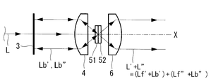
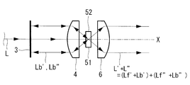
- a plurality of wavelength conversion elements 51 and 52 are provided.
- light of a plurality of colors may be generated from the blue laser light L.
- the light source device 1 includes two wavelength conversion elements 51 and 52 arranged in the direction along the optical axis X.
- the first wavelength conversion element 51 has the same characteristics as the wavelength conversion element 5 described above.
- the second wavelength conversion element 52 includes the wavelength 450 nm of the laser light L in the excitation wavelength band and a fluorescence L having a wavelength longer than that of the fluorescence L ′ generated by the first wavelength conversion element 51, for example, 650 nm. "Holding phosphor to generate”.
- the overlap between the emission wavelength bands of the wavelength conversion elements 51 and 52 and the excitation wavelength bands of the wavelength conversion elements 51 and 52 is small or not at all. Therefore, the fluorescence Lb ', Lb "hardly excites the phosphor to cause energy loss, and passes through the wavelength conversion elements 51, 52.
- the two wavelength conversion elements 51 and 52 may be arranged in the direction crossing the optical axis X, as shown in FIG. In this case, adjacent surfaces of the two wavelength conversion elements 51 and 52 are disposed substantially on the optical axis X such that the laser light L is incident on both of the wavelength conversion elements 51 and 52. Also in this case, as in the light source device 1, it is possible to simultaneously generate green fluorescence L ′ and red fluorescence L ′ ′ from the blue laser light L.
- wavelength conversion elements 51 and 52 it is not necessary to be one each of wavelength conversion elements 51 and 52, for example, one wavelength conversion element is 1 Alternatively, two wavelength conversion elements may be provided, and two wavelength conversion elements may be provided.
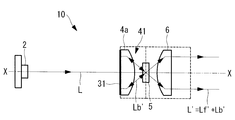
- the dichroic mirror 3 and the first collimating optical system 4 are separately configured, but instead, the light source device 10 according to the modification shown in FIG.
- the first collimating optical system 41 and the dichroic mirror 31 may be integrally formed.
- the first collimating optical system 41 includes a lens (a plano-convex lens in the illustrated example) 4a having a flat surface, and the dichroic mirror 31 is integrally formed on the flat surface of the lens 4a.
- the number of optical elements can be further reduced, and the optical path configuration can be further miniaturized.
- a plurality of wavelength conversion elements 51 and 52 as shown in FIGS. 2 and 3 may be employed.
- the lens surface disposed closest to the light source 2 among the lens surfaces of the lenses constituting the first collimating optical system 41 is a flat surface, and the dichroic mirror 31 is formed on the flat surface.
- a plurality of (two in the illustrated example) dichroic mirrors 3, 3 ', the first collimating optical system 4, 4 ', wavelength conversion elements 5, 5' and second collimating optics 6, 6 ' may be provided in series on the optical axis X.
- the wavelength conversion element 5 ′ of the latter group has a wavelength (for example, a peak wavelength of 650 nm) longer than the fluorescence L ′ generated by the wavelength conversion element 5 of the previous group.
- the second set of dichroic mirrors 3 'transmits the laser light L from the light source 2 and the fluorescence L' generated by the first set of wavelength conversion elements 5 and transmits the second set of It has a characteristic of reflecting the fluorescence L ′ ′ generated by the wavelength conversion element 5 ′. That is, as the wavelength conversion elements 5 and 5 'are disposed at positions farther from the light source 2 on the optical axis X, that is, as they are disposed downstream, the wavelength band of the generated light is longer. It is configured to hold the phosphor.
- FIG. 9 shows the wavelengths of the laser light L assumed in the configuration of the light source device 20, the wavelengths of the fluorescence L ′, L ′ ′ generated by the wavelength conversion elements 5, 5 ′, and the spectral transmission characteristics of the dichroic mirrors 3, 3 ′.
- the left vertical axis is the light transmittance of the dichroic mirror 3, 3 ′, and the right vertical axis is the relative intensity of the laser light L and the fluorescence L ′, L ′ ′.
- the laser light L that has passed through the wavelength conversion element 5 of the preceding set excites the wavelength conversion element 5 'of the subsequent set to emit light.
- a plurality of wavelength conversion elements 51 and 52 as shown in FIGS. 2 and 3 may be employed instead of the wavelength conversion elements 5 and 5 ′.
- the wavelength conversion element 5 is fixedly disposed in the optical path, but instead, a plurality of wavelength conversion elements are alternatively disposed in the optical path. It may be done.
- a plurality of wavelength conversion elements 51, 52, 53 may be provided on the rotation turret 7.
- the rotary turret 7 is arranged on the surface of the diffusion plate 8 in the circumferential direction around the central axis O, and the diffusion plate 8 transmits and diffuses light.
- the plurality of (three in the illustrated example) wavelength conversion elements 51, 52, and 53 that emit light of different colors according to the laser light L are provided.
- the rotary turret 7 is disposed in the optical path so that the central axis O is parallel to the optical axis X, and is rotated by a drive mechanism (not shown) around the central axis O, thereby turning one wavelength conversion element 51, 52, 53 It is configured to be disposed in the light path.
- the light source device 30 according to the modified example configured as described above, it is possible to easily switch the color of the output light to be finally generated.
- the light source device 1 includes the collimating optical systems 4 and 5.
- the configuration of the light source device is not limited to this, and the light source device 1 may not include the collimating optical system.
Landscapes
- Physics & Mathematics (AREA)
- Optics & Photonics (AREA)
- General Physics & Mathematics (AREA)
- Engineering & Computer Science (AREA)
- Condensed Matter Physics & Semiconductors (AREA)
- Spectroscopy & Molecular Physics (AREA)
- Multimedia (AREA)
- Signal Processing (AREA)
- Astronomy & Astrophysics (AREA)
- Electromagnetism (AREA)
- General Engineering & Computer Science (AREA)
- Projection Apparatus (AREA)
- Optical Elements Other Than Lenses (AREA)
- Lenses (AREA)
- Non-Portable Lighting Devices Or Systems Thereof (AREA)
- Semiconductor Lasers (AREA)
Abstract
光路構成が小型であるとともに高い効率で光を生成する。単色光(L)を出力する光源(2)と、該光源(2)の出力光軸(X)上に配置され、単色光(L)の照射によって該単色光(L)とは異なる色の光(L')を発生する波長変換素子(5)と、光源(2)と波長変換素子(5)との間に配置され、単色光(L)を透過し、波長変換素子(5)において発生された光(L')のうち光源2側に散乱した光(Lb')を波長変換素子(5)の方向に出力光軸(X)と平行に折り返すダイクロイックミラー(3)とを備える光源装置(1)を提供する。
Description
本発明は、光源装置に関するものである。
従来、半導体光源のような単一の色の光を出力する光源を用い、複数の色の光を生成する光源装置が知られている(例えば、特許文献1参照。)。特許文献1では、青色のレーザダイオード(LD)を光源として用い、青色の光を透過する領域と、青色の光によって赤色と緑色の蛍光を発生するとともにこれらの蛍光を反射する領域とを有する回転ホイールを備え、青色の光と赤色および緑色の光とを別々の光路で導光している。
しかしながら、特許文献1の場合、青色の光を導光する光路と、赤色および緑色の光を導光する光路とが別々に設けられているため、装置構成が大きくなり、部品点数も多くなるという問題がある。また、ミラーによって光路を複数回折り曲げているため、光を効率良く導光することができない。すなわち、光軸に対するミラーの角度がθずれていると、反射後の光の光軸の角度は2倍の2θずれることとなる。この光軸の角度のずれは、ミラーによって反射される度に累積される。また、ミラーによって反射される度に光は損失する。その結果、特許文献1の光路構成では、光源の出力に対して高い効率で光を生成して出力することができないという問題がある。
本発明は、上述した事情に鑑みてなされたものであって、光路構成が小型であるとともに高い効率で光を生成することができる光源装置を提供することを目的とする。
上記目的を達成するため、本発明は以下の手段を提供する。
本発明は、単色光を出力する光源と、該光源の出力光軸上に配置され、前記単色光が照射されることによって該単色光とは異なる色の光を発生する波長変換素子と、前記光源と前記波長変換素子との間に配置され、前記単色光を透過するとともに前記波長変換素子において発生された光のうち前記光源側に散乱した光を前記波長変換素子の方向に前記出力光軸と平行に折り返すダイクロイックミラーとを備える光源装置を提供する。
本発明は、単色光を出力する光源と、該光源の出力光軸上に配置され、前記単色光が照射されることによって該単色光とは異なる色の光を発生する波長変換素子と、前記光源と前記波長変換素子との間に配置され、前記単色光を透過するとともに前記波長変換素子において発生された光のうち前記光源側に散乱した光を前記波長変換素子の方向に前記出力光軸と平行に折り返すダイクロイックミラーとを備える光源装置を提供する。
本発明によれば、光源から出力された単色光は、波長変換素子において異なる色の光に変換された後に、出力光軸に沿って出力される。この場合に、波長変換素子において発生した光のうち光源側に散乱した一部の光は、単一のダイクロイックミラーによって出力光軸と平行に一度だけ折り返されて、光源とは反対側に散乱した他の光とともに出力される。したがって、変換後の光において光軸のずれや損失の発生が防止される。これにより、光源が出力した単色光から高効率で光を生成して出力することができる。また、光源、波長変換素子およびダイクロイックミラーは全て出力光軸上に一列に配置されているので、光路構成を小型にすることができる。
上記発明においては、前記ダイクロイックミラーと前記波長変換素子との間に配置され、該波長変換素子から前記光源側に散乱した光を平行光にする第1のコリメート光学系と、前記波長変換素子の後段に配置され、該波長変換素子から前記光源とは反対側に散乱した光を平行光にする第2のコリメート光学系とを備えた構成であってもよい。
このようにすることで、波長変換素子において発生して各方向に散乱した光を、第1のコリメート光学系および第2のコリメート光学系によって平行光にして出力することができる。
このようにすることで、波長変換素子において発生して各方向に散乱した光を、第1のコリメート光学系および第2のコリメート光学系によって平行光にして出力することができる。
上記構成においては、前記第1のコリメート光学系が、平面を有するレンズを備え、前記ダイクロイックミラーが、前記平面に一体的に形成されていてもよい。
このようにすることで、光学素子の数をさらに少なくし、光路構成をさらに小型にすることができる。
このようにすることで、光学素子の数をさらに少なくし、光路構成をさらに小型にすることができる。
上記発明においては、複数の前記波長変換素子が、前記出力光軸上の前記単色光の照射領域において、前記出力光軸に沿う方向にまたは交差する方向に配列されていてもよく、複数組の前記波長変換素子および前記ダイクロイックミラーが、前記出力光軸上に直列に配置されていてもよい。
このようにすることで、光源から出力された単色光から複数の色の光を生成することができる。
このようにすることで、光源から出力された単色光から複数の色の光を生成することができる。
本発明によれば、光路構成が小型であるとともに高い効率で光を生成することができるという効果を奏する。
以下に、本発明の一実施形態に係る光源装置1について図面を参照して説明する。
本実施形態に係る光源装置1は、図1に示されるように、単色光を出力する光源2と、該光源2の出力光軸X(以下、単に光軸Xともいう。)上に一列に配置されたダイクロイックミラー3、第1のコリメート光学系4、波長変換素子5および第2のコリメート光学系6とを備えている。
本実施形態に係る光源装置1は、図1に示されるように、単色光を出力する光源2と、該光源2の出力光軸X(以下、単に光軸Xともいう。)上に一列に配置されたダイクロイックミラー3、第1のコリメート光学系4、波長変換素子5および第2のコリメート光学系6とを備えている。
光源2は、指向性の高い単色のビーム光を出力する半導体光源やレーザダイオードなどである。本実施形態においては、単色のビーム光として、450nmの波長を有する青色のレーザ光Lを想定している。図1には単一の光源2が示されているが、レーザ光Lを互いに平行に出力する複数(例えば、2個×2個または3個×3個)の光源2がアレイ状に配置されていてもよい。
ダイクロイックミラー3は、光軸Xに対して垂直に配置され、光源2から入射してきたレーザ光Lを光軸Xに沿って透過する。また、ダイクロイックミラー3は、後述するように波長変換素子5において後方散乱した蛍光Lb’を光軸Xに沿って反射する。本実施形態においては、500nm以下の波長の光を透過し、500nmよりも長い波長の光を反射する特性を有するダイクロイックミラー3を想定している。図8は、本実施形態において想定されるレーザ光Lの波長と、波長変換素子5が発生する蛍光L’の波長(後述)と、ダイクロイックミラー3の分光透過特性との関係を示している。左縦軸はダイクロイックミラー3の光透過率であり、右縦軸はレーザ光Lおよび蛍光L’の相対強度である。
第1のコリメート光学系4は、凸面を光源2側に向けて配置されたメニスカスレンズまたは平凸レンズを備えている。第1のコリメート光学系4は、波長変換素子5において後方散乱された蛍光L’を平行化してダイクロイックミラー3へ出射する。また、第1のコリメート光学系4は、ダイクロイックミラー3によって反射されて戻ってきた蛍光L’を波長変換素子5に集光する。ここで、上記のようにメニスカスレンズまたは平凸レンズを、凸面を光源2側に向けて配置することによって、球面収差の発生を抑制することができる。第1のコリメート光学系4は、上記のメニスカスレンズまたは平凸レンズと図示しないレンズとを組み合わせた複数のレンズから構成されていることが望ましい。このようにすることで、球面収差の発生をさらに抑制することができる。
波長変換素子5は、光源2からのレーザ光L(単色光)が照射されることによって発光する素子であり、例えば、レーザ光Lによって励起される蛍光体または量子ドットを保持している。本実施形態においては、波長変換素子5として、レーザ光Lの波長450nmを励起波長帯域に含むとともに550nmのピーク波長を有する蛍光(光)L’を発生する蛍光体を想定している。波長変換素子5において発生した蛍光L’は、光軸Xの前方側(光源2とは反対側)の空間S1に前方散乱する蛍光Lf’と、光軸Xの後方側(光源2と同一側)の空間S2に後方散乱する蛍光Lb’とに分けられる。これら蛍光Lf’,Lb’のうち、前方散乱した蛍光Lf’は第2のコリメート光学系6へ入射し、後方散乱した蛍光Lb’は第1のコリメート光学系4へ入射する。
第2のコリメート光学系6は、凸面を光軸X前方に向けて配置された1つのメニスカスレンズまたは平凸レンズを備えている。第2のコリメート光学系6は、波長変換素子5から入射してきた蛍光L’を平行化し、光軸Xに沿って出射する。第2のコリメート光学系6は、上記のメニスカスレンズまたは平凸レンズと図示しないレンズとを組み合わせた複数のレンズから構成されていることが望ましい。このようにすることで、球面収差の発生をさらに抑制することができる。
次に、このように構成された光源装置1の作用について説明する。
本実施形態に係る光源装置1によれば、光源2から出力された青色のレーザ光Lがダイクロイックミラー3を透過して波長変換素子5に入射することによって、該波長変換素子5において緑色の蛍光L’が発生する。発生した蛍光L’のうち、前方散乱した蛍光Lf’は、第2のコリメート光学系6によって平行光に変換されてから光軸Xに沿って光源装置1の外部へ出力される。
本実施形態に係る光源装置1によれば、光源2から出力された青色のレーザ光Lがダイクロイックミラー3を透過して波長変換素子5に入射することによって、該波長変換素子5において緑色の蛍光L’が発生する。発生した蛍光L’のうち、前方散乱した蛍光Lf’は、第2のコリメート光学系6によって平行光に変換されてから光軸Xに沿って光源装置1の外部へ出力される。
一方、後方散乱して光軸Xを逆方向に進んだ蛍光Lb’は、第1のコリメート光学系4によって平行光に変換されてからダイクロイックミラー3によって折り返され、第1のコリメート光学系4によって波長変換素子5に集光される。ここで、波長変換素子5の発光波長帯域と励起波長帯域との重なりは少ないか、或いは全くない。したがって、波長変換素子5に集光された蛍光Lb’は、蛍光体を励起させてエネルギー損失を生じることは殆どなく、波長変換素子5を透過する。そして、波長変換素子5を透過した蛍光Lb’は、前方散乱した蛍光Lf’と同様に、第2のコリメート光学系6によって平行光に変換されてから光軸Xに沿って光源装置1の外部へ出力される。これにより、波長変換素子5において発生した蛍光L’全体が最終的な出力光として光源装置1から出力される。
この場合に、本実施形態によれば、光源2の出力光軸Xに沿って直線状に光路が形成され、後方散乱した蛍光Lb’が、光軸Xに垂直に配置された単一のダイクロイックミラー3によって光軸Xに平行な方向に、かつ、一度だけ反射される構成とされている。したがって、蛍光Lb’の光軸ずれおよび損失の発生が防止され、反射された蛍光Lb’は十分に高い効率で光軸Xに沿って光源装置1の外部へ出力される。これにより、レーザ光Lから出力光としての蛍光L’を高効率で生成することができるとうい利点がある。また、光路を直線状とすることによって、光路構成を小型にすることができるという利点がある。
なお、本実施形態においては、単一の波長変換素子5を備え、青色のレーザ光Lから緑色の蛍光L’を生成することとしたが、これに代えて、複数の波長変換素子51,52を備え、青色のレーザ光Lから複数の色の光を生成することとしてもよい。
図2に示される変形例に係る光源装置1は、光軸Xに沿う方向に配列された2つの波長変換素子51,52を備えている。第1の波長変換素子51は、上述した波長変換素子5と同一の特性を有している。第2の波長変換素子52は、レーザ光Lの波長450nmを励起波長帯域に含むとともに第1の波長変換素子51が発生する蛍光L’よりも長い波長、例えば、650nmのピーク波長を有する蛍光L”を発生する蛍光体を保持している。
ダイクロイックミラー3を透過してきた青色のレーザ光Lが第1の波長変換素子51および第2の波長変換素子52に入射すると、第1の波長変換素子51において緑色の蛍光L’が発生し、第2の波長変換素子52において赤色の蛍光L”が発生する。これら緑色の蛍光L’と赤色の蛍光L”のうち、前方散乱した蛍光Lf’,Lf”は第2のコリメート光学系6へ入射する。一方、後方散乱した蛍光Lb’,Lb”はダイクロイックミラー3で折り返されてから、第1のコリメート光学系4、第1の波長変換素子51および第2の波長変換素子52を通過し、第2のコリメート光学系6へ入射する。ここで、波長変換素子51,52の各発光波長帯域と波長変換素子51,52の各励起波長帯域との重なりは、少ないか、或いは全くない。したがって、蛍光Lb’,Lb”は、蛍光体を励起させてエネルギー損失を生じることは殆どなく、波長変換素子51,52を透過する。
このようにすることで、単色のレーザ光Lから、該レーザ光Lとは異なる2色の光L’,L”を同時に生成することができる。
2つの波長変換素子51,52は、図3に示されるように、光軸Xに交差する方向に配列されていてもよい。この場合、レーザ光Lが両方の波長変換素子51,52に入射するように、2つの波長変換素子51,52同士の隣接面が略光軸X上に配置される。このようにしても、光源装置1と同様に、青色のレーザ光Lから緑色の蛍光L’と赤色の蛍光L”とを同時に生成することができる。
2つの波長変換素子51,52は、図3に示されるように、光軸Xに交差する方向に配列されていてもよい。この場合、レーザ光Lが両方の波長変換素子51,52に入射するように、2つの波長変換素子51,52同士の隣接面が略光軸X上に配置される。このようにしても、光源装置1と同様に、青色のレーザ光Lから緑色の蛍光L’と赤色の蛍光L”とを同時に生成することができる。
また、図2および図3のように複数の波長変換素子51,52を備える構成においては、各波長変換素子51,52が1つずつである必要はなく、例えば、一方の波長変換素子を1つ、他方の波長変換素子を2つ備えていてもよく、各波長変換素子を2つずつ備えていてもよい。
また、本実施形態においては、ダイクロイックミラー3と第1のコリメート光学系4とが別体に構成されていることとしたが、これに代えて、図4に示される変形例に係る光源装置10のように、第1のコリメート光学系41とダイクロイックミラー31とが一体的に形成されていてもよい。この場合、第1のコリメート光学系41が平面を有するレンズ(図示する例では平凸レンズ)4aを備え、該レンズ4aの平面にダイクロイックミラー31が一体的に形成されていることが好ましい。
このように構成された変形例に係る光源装置10によれば、光学素子の数をさらに削減し、光路構成をさらに小型にすることができる。この構成においても、波長変換素子5に代えて、図2および図3に示されるような複数の波長変換素子51,52を採用してもよい。
このように構成された変形例に係る光源装置10によれば、光学素子の数をさらに削減し、光路構成をさらに小型にすることができる。この構成においても、波長変換素子5に代えて、図2および図3に示されるような複数の波長変換素子51,52を採用してもよい。
ここで、第1のコリメート光学系41を構成するレンズが有するレンズ面のうち最も光源2側に配されるレンズ面が平面であり、該平面にダイクロイックミラー31が形成されることが好ましい。これにより、後方散乱した蛍光Lb’は、第1のコリメート光学系41によって十分に平行光とされた状態でダイクロイックミラー31に入射することとなり、ダイクロイックミラー31による蛍光Lb’の反射効率を向上することができる。
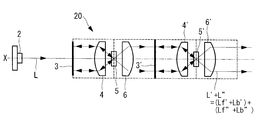
また、本実施形態においては、図5に示される変形例に係る光源装置20のように、複数組(図示する例では2組)のダイクロイックミラー3,3’、第1のコリメート光学系4,4’、波長変換素子5,5’および第2のコリメート光学系6,6’が、光軸X上に直列に備えられていてもよい。
この場合、後段の組の波長変換素子5’は、図2の波長変換素子52と同様に、前段の組の波長変換素子5が発生する蛍光L’よりも長い波長(例えば、650nmのピーク波長)を有する蛍光L”を発生する。後段の組のダイクロイックミラー3’は、光源2からのレーザ光Lおよび前段の組の波長変換素子5が発生した蛍光L’を透過し、後段の組の波長変換素子5’が発生した蛍光L”を反射するような特性を有する。すなわち、複数の波長変換素子5,5’は、光軸X上で光源2から離れた位置に配置されるほど、つまり後段側に配置されるほど、発生する光の波長帯域が長波長である蛍光体を保持するように構成されている。
図9は、光源装置20の構成において想定されるレーザ光Lの波長と、波長変換素子5,5’が発生する蛍光L’,L”の波長と、ダイクロイックミラー3,3’の分光透過特性との関係を示している。左縦軸はダイクロイックミラー3,3’の光透過率であり、右縦軸はレーザ光Lおよび蛍光L’,L”の相対強度である。
このようにして、前段の組の波長変換素子5を通過したレーザ光Lが、後段の組の波長変換素子5’を励起して発光させるようになっている。
この変形例に係る光源装置20においても、波長変換素子5,5’に代えて、図2および図3に示されるような複数の波長変換素子51,52を採用してもよい。
この変形例に係る光源装置20においても、波長変換素子5,5’に代えて、図2および図3に示されるような複数の波長変換素子51,52を採用してもよい。
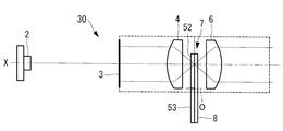
また、本実施形態においては、波長変換素子5が光路に固定配置されていることを前提としたが、これに代えて、複数の波長変換素子が択一的に光路に配されるように構成されていてもよい。例えば、図6に示されるように、複数の波長変換素子51,52,53が回転ターレット7に設けられていてもよい。
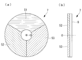
回転ターレット7は、図7の(a),(b)に示されるように、光を透過および拡散する拡散板8と、該拡散板8の表面に中心軸Oを中心にして周方向に配列して設けられ、レーザ光Lによって互いに異なる色の発光を呈する複数(図示する例では3つ)の波長変換素子51,52,53とを備えている。回転ターレット7は、中心軸Oが光軸Xと平行となるように光路に配置され、中心軸O回りに図示しない駆動機構によって回転させられることによって、一の波長変換素子51,52,53を光路に配するように構成されている。
このように構成された変形例に係る光源装置30によれば、最終的に生成する出力光の色を簡単に切り替えることができる。
このように構成された変形例に係る光源装置30によれば、最終的に生成する出力光の色を簡単に切り替えることができる。
また、本実施形態においては、波長変換素子5が保持する発光体の例として、蛍光体および量子ドットを挙げたが、波長変換素子5の例はこれに限定されるものではない。
また、本実施形態においては、光源装置1がコリメート光学系4,5を備えることとしていたが、光源装置の構成はこれに限定されるものではなく、コリメート光学系を備えない構成としてもよい。
また、本実施形態においては、光源装置1がコリメート光学系4,5を備えることとしていたが、光源装置の構成はこれに限定されるものではなく、コリメート光学系を備えない構成としてもよい。
1 光源装置
2 光源
3 ダイクロイックミラー
4 第1のコリメート光学系
5 波長変換素子
6 第2のコリメート光学系
L レーザ光(単色光)
L’ 蛍光(光)
X 出力光軸
2 光源
3 ダイクロイックミラー
4 第1のコリメート光学系
5 波長変換素子
6 第2のコリメート光学系
L レーザ光(単色光)
L’ 蛍光(光)
X 出力光軸
Claims (5)
- 単色光を出力する光源と、
該光源の出力光軸上に配置され、前記単色光が照射されることによって該単色光とは異なる色の光を発生する波長変換素子と、
前記光源と前記波長変換素子との間に配置され、前記単色光を透過するとともに前記波長変換素子において発生された光のうち前記光源側に散乱した光を前記波長変換素子の方向に前記出力光軸と平行に折り返すダイクロイックミラーとを備える光源装置。 - 前記ダイクロイックミラーと前記波長変換素子との間に配置され、該波長変換素子から前記光源側に散乱した光を平行光にする第1のコリメート光学系と、
前記波長変換素子の後段に配置され、該波長変換素子から前記光源とは反対側に散乱した光を平行光にする第2のコリメート光学系とを備える請求項1に記載の光源装置。 - 前記第1のコリメート光学系が、平面を有するレンズを備え、
前記ダイクロイックミラーが、前記平面に一体的に形成されている請求項2に記載の光源装置。 - 複数の前記波長変換素子が、前記出力光軸上の前記単色光の照射領域において、前記出力光軸に沿う方向にまたは交差する方向に配列されている請求項1から請求項3のいずれかに記載の光源装置。
- 複数組の前記波長変換素子および前記ダイクロイックミラーが、前記出力光軸上に直列に配置されている請求項1から請求項4のいずれかに記載の光源装置。
Priority Applications (1)
| Application Number | Priority Date | Filing Date | Title |
|---|---|---|---|
| US14/567,212 US20150138753A1 (en) | 2012-07-09 | 2014-12-11 | Light-source apparatus |
Applications Claiming Priority (2)
| Application Number | Priority Date | Filing Date | Title |
|---|---|---|---|
| JP2012153231A JP2014017344A (ja) | 2012-07-09 | 2012-07-09 | 光源装置 |
| JP2012-153231 | 2012-07-09 |
Related Child Applications (1)
| Application Number | Title | Priority Date | Filing Date |
|---|---|---|---|
| US14/567,212 Continuation US20150138753A1 (en) | 2012-07-09 | 2014-12-11 | Light-source apparatus |
Publications (1)
| Publication Number | Publication Date |
|---|---|
| WO2014010478A1 true WO2014010478A1 (ja) | 2014-01-16 |
Family
ID=49915939
Family Applications (1)
| Application Number | Title | Priority Date | Filing Date |
|---|---|---|---|
| PCT/JP2013/068214 WO2014010478A1 (ja) | 2012-07-09 | 2013-07-03 | 光源装置 |
Country Status (3)
| Country | Link |
|---|---|
| US (1) | US20150138753A1 (ja) |
| JP (1) | JP2014017344A (ja) |
| WO (1) | WO2014010478A1 (ja) |
Families Citing this family (3)
| Publication number | Priority date | Publication date | Assignee | Title |
|---|---|---|---|---|
| CN105008791B (zh) | 2013-08-06 | 2017-08-29 | 奥林巴斯株式会社 | 光源光学系统、光纤光源、显微镜和汽车用前照灯 |
| JP6493739B2 (ja) * | 2015-02-12 | 2019-04-03 | カシオ計算機株式会社 | 光源装置及び投影装置 |
| US10953797B2 (en) * | 2018-04-05 | 2021-03-23 | Toyota Motor Engineering & Manufacturing North America, Inc. | Cloaking devices with converging lenses and coherent image guides and vehicles comprising the same |
Citations (2)
| Publication number | Priority date | Publication date | Assignee | Title |
|---|---|---|---|---|
| JP2005347263A (ja) * | 2004-06-04 | 2005-12-15 | Lumileds Lighting Us Llc | 照明装置における離間した波長変換 |
| JP2010515096A (ja) * | 2006-12-29 | 2010-05-06 | フィリップス ルミレッズ ライティング カンパニー リミテッド ライアビリティ カンパニー | 不要な光をリサイクルするためのカラー選択パネルを含む照明デバイス |
Family Cites Families (7)
| Publication number | Priority date | Publication date | Assignee | Title |
|---|---|---|---|---|
| JP2003084168A (ja) * | 2001-09-14 | 2003-03-19 | Asahi Glass Co Ltd | 多層膜付レンズおよび光ファイバコリメータ |
| US7543959B2 (en) * | 2005-10-11 | 2009-06-09 | Philips Lumiled Lighting Company, Llc | Illumination system with optical concentrator and wavelength converting element |
| US20070236933A1 (en) * | 2006-04-06 | 2007-10-11 | Philips Lumileds Lighting Company Llc | Angular dependent element positioned for color tuning |
| JP2008040042A (ja) * | 2006-08-04 | 2008-02-21 | Toyota Central Res & Dev Lab Inc | 光学系及び光学装置 |
| US7902560B2 (en) * | 2006-12-15 | 2011-03-08 | Koninklijke Philips Electronics N.V. | Tunable white point light source using a wavelength converting element |
| US8567974B2 (en) * | 2008-02-27 | 2013-10-29 | Koninklijke Philips N.V. | Illumination device with LED and one or more transmissive windows |
| JP5659775B2 (ja) * | 2010-12-17 | 2015-01-28 | セイコーエプソン株式会社 | 光源装置及びプロジェクター |
-
2012
- 2012-07-09 JP JP2012153231A patent/JP2014017344A/ja active Pending
-
2013
- 2013-07-03 WO PCT/JP2013/068214 patent/WO2014010478A1/ja active Application Filing
-
2014
- 2014-12-11 US US14/567,212 patent/US20150138753A1/en not_active Abandoned
Patent Citations (2)
| Publication number | Priority date | Publication date | Assignee | Title |
|---|---|---|---|---|
| JP2005347263A (ja) * | 2004-06-04 | 2005-12-15 | Lumileds Lighting Us Llc | 照明装置における離間した波長変換 |
| JP2010515096A (ja) * | 2006-12-29 | 2010-05-06 | フィリップス ルミレッズ ライティング カンパニー リミテッド ライアビリティ カンパニー | 不要な光をリサイクルするためのカラー選択パネルを含む照明デバイス |
Also Published As
| Publication number | Publication date |
|---|---|
| US20150138753A1 (en) | 2015-05-21 |
| JP2014017344A (ja) | 2014-01-30 |
Similar Documents
| Publication | Publication Date | Title |
|---|---|---|
| KR102088741B1 (ko) | 발광 장치 및 프로젝션 시스템 | |
| US9677720B2 (en) | Lighting device comprising a wavelength conversion arrangement | |
| US9781394B2 (en) | Lighting device having phosphor wheel and excitation radiation source | |
| JP6215989B2 (ja) | 照明システム及び投影装置 | |
| JP5959342B2 (ja) | 光源装置 | |
| US9904160B2 (en) | Light-emitting device and related light source system | |
| KR100403599B1 (ko) | 조명계 및 이를 채용한 프로젝션 시스템 | |
| US9651220B2 (en) | Light module for generating wavelength-converted light | |
| EP3499309A1 (en) | Light-source system and projection device | |
| CN109491187B (zh) | 波长转换装置、光源系统及投影设备 | |
| WO2014109333A1 (ja) | 波長変換デバイス、照明光学系およびこれを用いた電子装置 | |
| TWM552112U (zh) | 光源裝置及投影系統 | |
| JP2012141411A (ja) | 光源装置 | |
| CN109557753B (zh) | 光源系统及投影装置 | |
| JP2017215570A (ja) | 光源装置およびプロジェクター | |
| CN113359379A (zh) | 光源组件及投影设备 | |
| WO2014010478A1 (ja) | 光源装置 | |
| RU2010154659A (ru) | Светоизлучающее устройство и способ излучения света | |
| CN110297384B (zh) | 一种用于投影的光源 | |
| JP6236744B2 (ja) | 光源装置、照明光学系及び画像表示装置 | |
| JP6741380B2 (ja) | 光源及び投影システム | |
| US20090168186A1 (en) | Device and method for reducing etendue in a diode laser | |
| JP2012094439A (ja) | 照明装置および投影型映像表示装置 | |
| JP6771932B2 (ja) | 二重光源改良型統合システム | |
| JP6711705B2 (ja) | 照明装置およびこれを用いた投射型表示装置 |
Legal Events
| Date | Code | Title | Description |
|---|---|---|---|
| 121 | Ep: the epo has been informed by wipo that ep was designated in this application |
Ref document number: 13817572 Country of ref document: EP Kind code of ref document: A1 |
|
| NENP | Non-entry into the national phase |
Ref country code: DE |
|
| 122 | Ep: pct application non-entry in european phase |
Ref document number: 13817572 Country of ref document: EP Kind code of ref document: A1 |