WO2014010037A1 - 波長合分波器、光モジュールおよびそれを用いたサーバ - Google Patents
波長合分波器、光モジュールおよびそれを用いたサーバ Download PDFInfo
- Publication number
- WO2014010037A1 WO2014010037A1 PCT/JP2012/067643 JP2012067643W WO2014010037A1 WO 2014010037 A1 WO2014010037 A1 WO 2014010037A1 JP 2012067643 W JP2012067643 W JP 2012067643W WO 2014010037 A1 WO2014010037 A1 WO 2014010037A1
- Authority
- WO
- WIPO (PCT)
- Prior art keywords
- slab waveguide
- light
- diffraction grating
- wavelength
- optical module
- Prior art date
- Legal status (The legal status is an assumption and is not a legal conclusion. Google has not performed a legal analysis and makes no representation as to the accuracy of the status listed.)
- Ceased
Links
Images






Classifications
-
- G—PHYSICS
- G02—OPTICS
- G02B—OPTICAL ELEMENTS, SYSTEMS OR APPARATUS
- G02B6/00—Light guides; Structural details of arrangements comprising light guides and other optical elements, e.g. couplings
- G02B6/24—Coupling light guides
- G02B6/42—Coupling light guides with opto-electronic elements
- G02B6/4201—Packages, e.g. shape, construction, internal or external details
- G02B6/4204—Packages, e.g. shape, construction, internal or external details the coupling comprising intermediate optical elements, e.g. lenses, holograms
- G02B6/4215—Packages, e.g. shape, construction, internal or external details the coupling comprising intermediate optical elements, e.g. lenses, holograms the intermediate optical elements being wavelength selective optical elements, e.g. variable wavelength optical modules or wavelength lockers
-
- G—PHYSICS
- G02—OPTICS
- G02B—OPTICAL ELEMENTS, SYSTEMS OR APPARATUS
- G02B6/00—Light guides; Structural details of arrangements comprising light guides and other optical elements, e.g. couplings
- G02B6/10—Light guides; Structural details of arrangements comprising light guides and other optical elements, e.g. couplings of the optical waveguide type
- G02B6/12—Light guides; Structural details of arrangements comprising light guides and other optical elements, e.g. couplings of the optical waveguide type of the integrated circuit kind
- G02B6/122—Basic optical elements, e.g. light-guiding paths
- G02B6/124—Geodesic lenses or integrated gratings
-
- G—PHYSICS
- G02—OPTICS
- G02B—OPTICAL ELEMENTS, SYSTEMS OR APPARATUS
- G02B6/00—Light guides; Structural details of arrangements comprising light guides and other optical elements, e.g. couplings
- G02B6/24—Coupling light guides
- G02B6/26—Optical coupling means
- G02B6/28—Optical coupling means having data bus means, i.e. plural waveguides interconnected and providing an inherently bidirectional system by mixing and splitting signals
- G02B6/293—Optical coupling means having data bus means, i.e. plural waveguides interconnected and providing an inherently bidirectional system by mixing and splitting signals with wavelength selective means
- G02B6/29304—Optical coupling means having data bus means, i.e. plural waveguides interconnected and providing an inherently bidirectional system by mixing and splitting signals with wavelength selective means operating by diffraction, e.g. grating
- G02B6/29305—Optical coupling means having data bus means, i.e. plural waveguides interconnected and providing an inherently bidirectional system by mixing and splitting signals with wavelength selective means operating by diffraction, e.g. grating as bulk element, i.e. free space arrangement external to a light guide
- G02B6/29308—Diffractive element having focusing properties, e.g. curved gratings
-
- G—PHYSICS
- G02—OPTICS
- G02B—OPTICAL ELEMENTS, SYSTEMS OR APPARATUS
- G02B6/00—Light guides; Structural details of arrangements comprising light guides and other optical elements, e.g. couplings
- G02B6/24—Coupling light guides
- G02B6/26—Optical coupling means
- G02B6/30—Optical coupling means for use between fibre and thin-film device
-
- G—PHYSICS
- G02—OPTICS
- G02B—OPTICAL ELEMENTS, SYSTEMS OR APPARATUS
- G02B6/00—Light guides; Structural details of arrangements comprising light guides and other optical elements, e.g. couplings
- G02B6/24—Coupling light guides
- G02B6/26—Optical coupling means
- G02B6/34—Optical coupling means utilising prism or grating
-
- G—PHYSICS
- G02—OPTICS
- G02B—OPTICAL ELEMENTS, SYSTEMS OR APPARATUS
- G02B6/00—Light guides; Structural details of arrangements comprising light guides and other optical elements, e.g. couplings
- G02B6/24—Coupling light guides
- G02B6/42—Coupling light guides with opto-electronic elements
- G02B6/4201—Packages, e.g. shape, construction, internal or external details
- G02B6/4246—Bidirectionally operating package structures
-
- G—PHYSICS
- G02—OPTICS
- G02B—OPTICAL ELEMENTS, SYSTEMS OR APPARATUS
- G02B6/00—Light guides; Structural details of arrangements comprising light guides and other optical elements, e.g. couplings
- G02B6/24—Coupling light guides
- G02B6/42—Coupling light guides with opto-electronic elements
- G02B6/43—Arrangements comprising a plurality of opto-electronic elements and associated optical interconnections
Definitions
- the present invention relates to a wavelength multiplexer / demultiplexer, and more particularly, to a wavelength multiplexing / demultiplexing device for wavelength multiplexing optical transmission, an optical module, and a server that transmit light of a plurality of wavelengths using a single optical fiber.
- Wavelength multiplex transmission is a method in which light of a plurality of wavelengths independently transmits a signal to a single transmission line, and can achieve a capacity increase of several times the wavelength.
- the transmitter has a plurality of light sources of different wavelengths and a multiplexing function for bundling them, and the receiver is configured by a function of separating light of a plurality of different wavelengths and a receiving element for receiving the separated optical signal.
- silicon photonics is attracting attention as a technology for realizing optical interconnection. Silicon photonics is a technology that uses Si as an optical element, and since highly developed silicon process technology can be used, fine processing and mass production are possible. Research and development of wavelength multiplex transmission transmitters and receivers using this silicon photonics technology is progressing.
- Non-Patent Document 1 reports a multiplexing function that bundles light of different wavelengths using a silicon photonics technology and a demultiplexing functional device that separates light of different wavelengths.
- the wavelength multiplexer / demultiplexer according to this technology is a slab waveguide having a parallel plate structure made of silicon, a reflective diffraction grating adjacent to the slab waveguide, and a side opposite to the reflective diffraction grating. And a plurality of waveguides for input and output. Further, in the multiplexer / demultiplexer disclosed in Patent Document 1, the slab waveguide is formed of a photonic crystal. The characteristics of these wavelength multiplexers / demultiplexers are shown in FIG.
- This characteristic indicates a wavelength multiplexing / demultiplexing function conforming to 100GBASE-ER4 and 100GBASE-LR4 of IEEE 802.3ba, which is a standard of Ethernet (registered trademark). That is, a wavelength multiplexer / demultiplexer having a wavelength multiplexing / demultiplexing function satisfying the wavelength interval 4.5 nm, passband 2.3 nm, and 4-wave multiplexing standards is realized.
- the slab waveguide that constitutes the wavelength multiplexer / demultiplexer is made of silicon, but the temperature dependence of the refractive index of silicon is large, so that the operating temperature changes.
- the wavelength multiplexing / demultiplexing characteristics change greatly.
- the wavelength characteristic is very sensitive to the refractive index, that is, the temperature, a normal operation cannot be performed due to the large fluctuation of the operating temperature.
- An object of the present invention relates to a wavelength multiplexing / demultiplexing device which is a multiplexing function for bundling light of different wavelengths and a demultiplexing functional device for separating light of different wavelengths in a transmitter and a receiver for realizing optical interconnection.
- An object of the present invention is to provide an optical module or a wavelength multiplexer / demultiplexer that does not require a temperature adjustment function whose characteristics do not change with respect to changes.
- a diffraction grating is provided on the inner wall on the side facing the entrance opening, which is provided on the board and has a plurality of entrance openings and one exit opening.
- a plurality of light receiving elements that receive light having different wavelengths emitted from the waveguide, and the light incident on the first slab waveguide is reflected by the diffraction grating in the slab waveguide and combined.
- the second The light incident on the Love waveguide is demultiplexed reflected by the diffraction grating in the second slab waveguide, characterized in that it is emitted from the exit of the second slab waveguide.
- an optical module and a server capable of reducing power consumption can be provided.
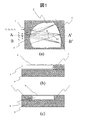
- FIG. 1 is a diagram of a wavelength multiplexer / demultiplexer according to a first embodiment of the present invention.
- FIG. 1 (a) is a top view and
- FIG. 1 (b) is an AA ′ cross section of FIG. 1 (a).
- FIG. 1 and FIG. 1C are BB ′ cross-sectional views of FIG.
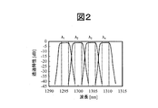
- FIG. 2 is a diagram showing the wavelength transmission characteristics of the wavelength multiplexer / demultiplexer of the present invention.
- FIG. 3 is a diagram showing the environmental temperature dependence of the wavelength characteristic change according to the present invention and the conventional example.
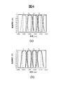
- FIG. 4 is a diagram showing a change in transmission characteristics due to a change in ambient temperature of the wavelength transmission characteristics of the wavelength multiplexer / demultiplexer.
- FIG. 1 is a diagram of a wavelength multiplexer / demultiplexer according to a first embodiment of the present invention.
- FIG. 1 (a) is a top view and
- FIG. 1 (b) is an AA ′
- FIG. 4A is a diagram showing a change in transmission characteristic due to a change in environmental temperature according to a conventional example
- FIG. 4B is a diagram showing a change in transmission characteristic due to a change in environmental temperature according to the present invention.
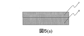
- FIG. 5A is a diagram showing a manufacturing process of the first embodiment of the present invention.
- FIG. 5B is a diagram showing a manufacturing process of the first embodiment of the present invention.
- FIG. 5C is a diagram showing a manufacturing process of the first embodiment of the present invention.
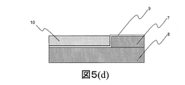
- FIG. 5D is a diagram showing a manufacturing process of the first embodiment of the present invention.
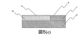
- FIG. 5 (e) is a diagram showing a manufacturing process of the first embodiment of the present invention.
- FIG. 5 (e) is a diagram showing a manufacturing process of the first embodiment of the present invention.
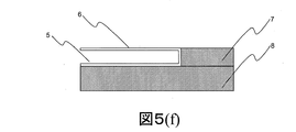
- FIG. 5 (f) is a diagram showing a manufacturing process of the first embodiment of the present invention.
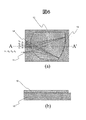
- FIG. 6 is a diagram of a wavelength multiplexer / demultiplexer according to a second embodiment of the present invention.
- FIG. 2 (a) is a top view
- FIG. 2 (b) is an AA ′ cross section of FIG. 2 (a).
- FIG. 7A is a structural diagram of a transceiver using the wavelength multiplexer / demultiplexer according to the third embodiment of the present invention.
- FIG. 7B is a structural diagram of a transceiver using a wavelength multiplexer / demultiplexer according to the third embodiment of the present invention.
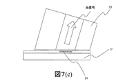
- FIG. 7 (c) is a structural diagram of a transceiver using a wavelength multiplexer / demultiplexer according to the third embodiment of the present invention.
- FIG. 8 is a structural diagram of a server and a packet optical transport device using backplane optical interconnection by a transceiver using a wavelength multiplexer / demultiplexer according to a fourth embodiment of the present invention.
- the wavelength demultiplexing function according to the present invention will be described with reference to FIG.
- the present invention is an echelle grating, that is, a wavelength multiplexer / demultiplexer using a diffraction grating having a diffraction order of 2 or more.
- Lights having wavelengths ⁇ 1 , ⁇ 2 , ⁇ 3 , and ⁇ 4 are incident on the slab waveguide 2 constituted by the air core from the optical waveguide 1 for input.
- the light incident on the slab waveguide spreads by diffraction in the plane of FIG. 1A and enters the diffraction grating 3 at an angle ⁇ i .
- the light incident on the diffraction grating 3 is diffracted at an angle of ⁇ d for each wavelength according to the equation (1), and enters the optical waveguide 4 for output corresponding to each wavelength.
- the relationship between the wavelength and the diffraction angle is as follows.
- ⁇ i is the incident angle of the light incident on the diffraction grating with respect to the diffraction grating
- ⁇ d is the diffraction angle of the light diffracted from the diffraction grating with respect to the diffraction grating
- m is the diffraction
- ⁇ is the wavelength of light
- n eff (T) is the effective refractive index of the slab waveguide and is a function of temperature.
- Light of wavelength ⁇ incident on the diffraction grating at an angle ⁇ i from the slab waveguide is diffracted by the diffraction grating, diffracted at an angle ⁇ d and guided to the waveguide for emission.
- the outlet side of the waveguide is Formed at an angle of the theta d as the light of the wavelength ⁇ can condensing.
- the effective refractive index n eff (T) changes. Since the period d of the diffraction grating, the incident angle ⁇ i of light incident on the diffraction grating, the angle ⁇ d of the waveguide on the exit side, and the diffraction order m do not change, the wavelength ⁇ changes and becomes ⁇ ′. That is, light of wavelength ⁇ ′ is collected in a wavelength demultiplexer designed to collect wavelength ⁇ . The amount of change ⁇ of the wavelength ⁇ ′ from ⁇ depends on the effective refractive index n eff (T). If the change of n eff (T) is small, the amount of change ⁇ has no problem with the actual use conditions.
- FIG. 3 shows the temperature change dependency of the wavelength change when silicon and air having such characteristics are used in the slab waveguide.
- the temperature change under actual use conditions is 100 degrees.
- the wavelength change amount ⁇ is 6.5 nm.
- the wavelength change ⁇ is 0.1 nm, which satisfies the wavelength change of 1 nm or less under the use conditions.
- the wavelength change ⁇ with respect to a temperature change of 100 degrees is 0.7 nm, which satisfies the wavelength change of 1 nm or less under the use conditions.
- a multiplexing function that bundles light of different wavelengths and a wavelength multiplexer / demultiplexer that is a demultiplexing function device that separates light of different wavelengths
- a wavelength multiplexer / demultiplexer that does not require a temperature adjustment function whose characteristics do not change with environmental temperature changes.
- FIG. 1 is a structural diagram of a wavelength multiplexer / demultiplexer according to a first embodiment of the present invention.
- 1A is a top view
- FIG. 1B is a cross-sectional view along A-A ′ in FIG. 1A
- FIG. 1C is a cross-sectional view along B-B ′ in FIG.
- an optical waveguide 1 for input formed on an SOI (Silicon on Insulator), a slab waveguide 2 composed of a metal 6 and an air core 5, a diffraction grating 3, and an output of demultiplexed light. It is comprised by the optical waveguide 4 for.
- SOI Silicon on Insulator
- the wavelength multiplexer / demultiplexer of FIG. 1 is used as a wavelength demultiplexer.
- Lights having wavelengths ⁇ 1 , ⁇ 2 , ⁇ 3 , and ⁇ 4 are incident on the slab waveguide 2 constituted by the air core from the optical waveguide 1 for input.
- the light incident on the slab waveguide spreads by diffraction in the plane of FIG. 1A and enters the diffraction grating 3 at an angle ⁇ i .
- the light incident on the diffraction grating 3 is diffracted at an angle of ⁇ d for each wavelength according to the equation (1), and enters the optical waveguide 4 for output corresponding to each wavelength.
- the optical waveguide 1 for input and the optical waveguide 4 for output are optically connected to the slab waveguide 2 on the circumference of the radius R.
- the diffraction grating 3 has a curvature with a radius of 2R, and is in contact with the radius R which is a connecting surface between the waveguide 1 for input and the waveguide 4 for output and the slab waveguide 2 described above.
- wavelength multiplexer / demultiplexer When this wavelength multiplexer / demultiplexer is used as a wavelength multiplexer, the reverse optical path of the wavelength demultiplexer is followed.
- Lights of wavelengths ⁇ 1 , ⁇ 2 , ⁇ 3 , and ⁇ 4 are input from the optical waveguide 4 for outputting light and are incident on the slab waveguide 2.
- the light incident on the slab waveguide spreads by diffraction in the plane of FIG. 1A and enters the diffraction grating 3 at an angle ⁇ d corresponding to each wavelength.
- the light incident on the diffraction grating 3 is diffracted at an angle ⁇ i according to the equation (1), and enters the optical waveguide 1.
- the silicon 7 on the silicon oxide film 8 is etched by a photoetching process to form a groove shown in FIG.
- channel is as showing to Fig.1 (a).
- a metal thin film 9 is formed.
- the metal thin film 9 is formed not only on the silicon oxide film 8 but also on the side surface of the silicon 7.
- the trench formed in FIG. After forming the sacrificial layer 10, the metal thin film 9 is formed on the sacrificial layer 10.
- the sacrificial layer 10 is removed by etching to form a waveguide composed of the metal thin film 9 and the air core 5 which are parallel flat plates as shown in FIG.
- the width of the optical waveguide 1 for input is 5 to 20 ⁇ m
- the width of the optical waveguide 4 for output is 5 to 20 ⁇ m.
- the narrow side is a request from the manufacturing error when manufacturing the optical waveguide
- the wide side is a request from the size of the wavelength multiplexer / demultiplexer.
- the order of the diffraction grating is 2 to 40.
- Fig. 2 shows the demultiplexing characteristics of the fabricated wavelength demultiplexer. Centering on wavelengths of 1295.6 nm, 1300.1 nm, 1304.6 nm, and 1309.1 nm, excellent demultiplexing characteristics are shown at 2.3 nm or more as passbands.
- the characteristic indicated by the solid line in FIG. 4B was shown. That is, the wavelength characteristic was shifted by 0.1 nn to the long wavelength side. This wavelength shift amount of 0.1 nm satisfies the wavelength change amount of 1 nm or less under the use conditions.
- FIG. 6 is a structural diagram of a wavelength multiplexer / demultiplexer according to the second embodiment of the present invention.
- 6A is a top view
- FIG. 6B is a cross-sectional view taken along the line AA in FIG. 6A.
- an optical waveguide 14 for input formed on an SOI (Silicon on Insulator), a slab waveguide 12 composed of silicon nitride 16, a diffraction grating 13, and an output for combined light. It is constituted by the optical waveguide 11.
- SOI Silicon on Insulator
- the wavelength multiplexer / demultiplexer of FIG. 6 is used as a wavelength multiplexer.
- Light having wavelengths ⁇ 1 , ⁇ 2 , ⁇ 3 , and ⁇ 4 is incident on the slab waveguide 12 made of silicon nitride from the optical waveguide 14 for input.
- the light incident on the slab waveguide spreads by diffraction in the plane of FIG.
- the optical waveguide 14 for input and the optical waveguide 11 for output exist on a curve having a radius of curvature R and are optically connected to the slab waveguide 12 on the circumference of the radius R.
- the diffraction grating 13 has a radius of curvature of 2R, and is in contact with the aforementioned waveguide 14 for input and the radius R which is a connection surface between the waveguide 11 for output and the slab waveguide 12.
- the width of the optical waveguide 1 for input is 5 to 20 ⁇ m
- the width of the optical waveguide 4 for output is 5 to 20 ⁇ m.
- the order of the diffraction grating is 2 to 40.
- this wavelength multiplexer / demultiplexer When this wavelength multiplexer / demultiplexer is used as a wavelength multiplexer, the reverse optical path of the wavelength demultiplexer is followed.
- Light having wavelengths ⁇ 1 , ⁇ 2 , ⁇ 3 , and ⁇ 4 is incident on a slab waveguide 12 made of silicon nitride from an optical waveguide 11 for input.
- the light incident on the slab waveguide spreads by diffraction in the plane of FIG. 6A and enters the diffraction grating 13 at an angle ⁇ i .
- the light incident on the diffraction grating 13 is diffracted at an angle of ⁇ d for each wavelength according to the equation (1), and enters the optical waveguide 14 for output corresponding to each wavelength.
- the optical waveguide 11 for input and the optical waveguide 14 for output are optically connected to the slab waveguide 12 on the circumference of the radius R.
- the diffraction grating 13 has a curvature with a radius of 2R, and is in contact with the aforementioned waveguide 11 for input and the radius R which is a connection surface between the waveguide 14 for output and the slab waveguide 12.
- Fig. 2 shows the demultiplexing characteristics of the fabricated wavelength demultiplexer. Centering on wavelengths of 1295.6 nm, 1300.1 nm, 1304.6 nm, and 1309.1 nm, excellent demultiplexing characteristics are shown at 2.3 nm or more as passbands. When the temperature of the wavelength demultiplexer was raised by 100 degrees and the wavelength demultiplexing characteristics were examined in the same manner, the wavelength characteristics were shifted by 0.1 nn to the long wavelength side. This wavelength shift amount of 0.7 nm satisfies the wavelength change amount of 1 nm or less under use conditions.
- FIG. 7A is a structural diagram of a transceiver using a wavelength multiplexer / demultiplexer according to the third embodiment of the present invention
- FIG. 7B is a top view of the grating coupler 24
- FIG. 3 is an enlarged cross-sectional view of a connecting portion between a grating coupler 24 and an optical fiber 23.
- FIG. 7A is a structural diagram of a transceiver using a wavelength multiplexer / demultiplexer according to the third embodiment of the present invention
- FIG. 7B is a top view of the grating coupler 24
- FIG. 3 is an enlarged cross-sectional view of a connecting portion between a grating coupler 24 and an optical fiber 23.
- FIG. 7A is a structural diagram of a transceiver using a wavelength multiplexer / demultiplexer according to the third embodiment of the present invention
- FIG. 7B is a top view of the grating coupler 24
- FIG. 3 is an enlarged cross-
- This structure is a transceiver that transmits and receives 8-wavelength signal light.
- an 8-wavelength semiconductor laser array 18 mounted on an SOI substrate 17, eight input optical waveguides 19 corresponding to each wavelength, and signal light having different input wavelengths are multiplexed.
- Wavelength multiplexer 20 output optical waveguide 21 of the combined light, grating coupler 22 for coupling signal light to the fiber, optical fiber 23, grating coupler 24 for coupling signal light from the fiber, 8 wavelengths
- An optical waveguide 25 for inputting the signal light consisting of the above into the demultiplexer, a wavelength demultiplexer 26 for demultiplexing the input optical signals of different wavelengths for each wavelength, and eight light beams for demultiplexing for each wavelength
- An output optical waveguide 27 and a photodiode array 28 for detecting light are included. Light emitted from the 8-wavelength semiconductor laser array 18 mounted on the SOI substrate 17 is input to the wavelength multiplexer 20 via the input waveguide 19.
- the lights incident from the eight input optical waveguides 19 corresponding to the respective wavelengths are multiplexed and output to the output optical waveguide 21.
- the signal light having eight wavelengths guided to the output optical waveguide 21 is input to the grating coupler 22 for coupling the signal light to the fiber.
- the grating coupler 22 has a structure shown in FIG.
- the grating coupler 22 is formed so that the input signal light is emitted at a desired angle in the upper surface direction, and the light emitted from the grating coupler 22 is input to the fiber 23 as shown in FIG.
- the signal light is output from the transceiver.
- light input from the outside to the transmitter / receiver is input from the fiber 23 to the grating coupler 24 and input to the wavelength demultiplexer 26 via the optical waveguide 25 for input.
- the light is demultiplexed and input to the eight output optical waveguides 26 corresponding to the respective wavelengths, and is input to the photodiode array 28 that detects light, and the optical signal is detected.
- a semiconductor laser that oscillates in a single mode in the vertical and horizontal directions is used as input light. Since the light emitted from the semiconductor laser 18 has a constant polarization and is stable, the polarization of the light input to the wavelength multiplexer 20 via the input waveguide 19 is also single and stable.
- the distance from the incident waveguide to the diffraction grating can be set to 200 to 600 ⁇ m.
- the plane of polarization of the light input from the fiber 23 is random.
- the wavelength demultiplexer 26 needs to be independent of polarization, and the distance from the incident waveguide to the diffraction grating needs to be 1 to 4 mm. Therefore, even in the same transmitter / receiver, the wavelength demultiplexer needs to be larger in size than the wavelength multiplexer. As described above, the wavelength multiplexer 20 and the wavelength demultiplexer 26 are different in size.
- the transmitter / receiver using the wavelength multiplexer / demultiplexer thus manufactured succeeded in transmitting / receiving eight-wave signal light in a temperature range of environmental temperature fluctuation of 100 degrees.
- FIG. 8 is a structural diagram of a server and a packet optical transport device using backplane optical interconnection by a transceiver using a wavelength multiplexer / demultiplexer according to a fourth embodiment of the present invention.
- the apparatus according to the present embodiment includes a plurality of interface cards 29 and a switch card 30, which are connected by a fiber 32 on the backplane, and signals are transmitted and received. Specifically, a signal input from the outside of the apparatus via the optical fiber 33 is converted into an electric signal by the optical transceiver 34 and processed by the integrated circuit 35. The signal-processed electrical signal is converted into an optical signal by the optical transceiver 31 and sent to the switch card 30 via the optical fiber 32.
- a signal converted into an electric signal by the transmitter / receiver 31 on the switch card 30 is switched to a path corresponding to the signal by the switching element 36, and an output thereof is converted into an optical signal by the transmitter / receiver 31, and is interfaced via the optical fiber 31. Input to the card 29.
- This optical signal is converted into an electrical signal by the optical transmitter / receiver 31, then signal-processed by the integrated circuit 35, converted again to an optical signal by the optical transmitter / receiver 34, and output through the optical fiber 33.
- the optical transceiver 31 at this time uses the optical transceiver 31 that does not require temperature adjustment using the wavelength multiplexer / demultiplexer described in the fourth embodiment.
- a transceiver that does not require a temperature adjustment function that does not change the transmission / reception characteristics of an optical signal even if there is no temperature adjustment mechanism with respect to environmental temperature changes, a large capacity can be achieved while simultaneously reducing power consumption.
- a server capable of operating power and a packet optical transport device can be provided.
- wavelength multiplexing / demultiplexing devices which are multiplexing functions that bundle light of different wavelengths and demultiplexing functional devices that separate light of different wavelengths, in transmitters and receivers that realize optical interconnection, characteristics are affected by changes in operating temperature.
- a wavelength multiplexer / demultiplexer that does not require a temperature control function that does not change can be provided.
- Optical waveguide 2 for input 12... Slab waveguide, 3, 13 ... Diffraction grating, 4, 11, 21, 27 ... optical waveguide for output, 5 ... Air core, 6 ... metal, 7 ... Silicon, 8 ... Silicon oxide film, 9 ... metal thin film, 10 ... Sacrificial layer, 16 ... silicon nitride core, 17 ... SOI substrate, 18 ... Semiconductor laser array, 20: Wavelength multiplexer, 22, 24 ... Grating coupler, 23, 32, 33 ... optical fiber, 26: Wavelength demultiplexer, 28 ... photodiode array, 29 ... Interface card, 30 ... switch card, 31, 34 ... Optical transceiver 35 ... Integrated circuit 36 ... Switching element
Landscapes
- Physics & Mathematics (AREA)
- General Physics & Mathematics (AREA)
- Optics & Photonics (AREA)
- Engineering & Computer Science (AREA)
- Microelectronics & Electronic Packaging (AREA)
- Optical Integrated Circuits (AREA)
- Optical Communication System (AREA)
- Optical Couplings Of Light Guides (AREA)
Description
本発明は、波長合分波器に係り、特に、1本の光ファイバで複数の波長の光を伝送する波長多重光伝送用波長合分波器、光モジュール、及びサーバの構造に関する。
高度情報化社会の進展とともに、ネットワークを流れる情報の伝達量は年率40%の割合で上昇し、この大容量の情報を処理するサーバやデータセンタを支える演算処理装置の高速化、高機能化が求められている。このため、この情報処理装置には、大容量化、小型化、低消費電力化が求められ、そのアプローチのひとつとしてインターコネクションの光化が進められている。光インターコネクションにおいて、大容量化を実現するための方法として波長多重伝送が有力な候補である。波長多重伝送とは、1本の伝送路に複数の波長の光がそれぞれ独立に信号を伝達する方法で、波長数倍の大容量化が実現できる。その送信器は複数の異なる波長の光源とそれらを束ねる多重機能を有し、受信器は、複数の異なる波長の光を分離する機能と、分離後の光信号を受信する受信素子により構成される。一方、光インターコネクションを実現する技術として、シリコンフォトニクスが注目されている。シリコンフォトニクスはSiを光素子として用いる技術で、高度に発達したシリコンプロセス技術を用いることができるため、微細加工、大量一括生産が可能である。このシリコンフォトニクスの技術を用いた波長多重伝送の送信器、受信器の研究開発が進んでいる。
たとえば、非特許文献1では、シリコンフォトニクス技術を用いた異なる波長の光を束ねる多重機能及び異なる波長の光を分離する分波機能デバイスが報告されている。この技術による波長合分波器は、シリコンにより構成された導波路断面が平行平板構造をしているスラブ導波路と、そのスラブ導波路に隣接した反射型回折格子、反射型回折格子の対抗側に入出力用の複数の導波路から構成されている。また、特許文献1開示されている合分波器では、スラブ導波路がフォトニック結晶により構成されている。これらの波長合分波器の特性を図2に示す。この特性は、イーサネット(登録商標)の標準化規格であるIEEE802.3baの100GBASE-ER4及び100GBASE-LR4に適合する波長合分波機能を示している。すなわち、波長間隔4.5nm、パスバンド2.3nm、4波多重の規格を満たす波長合分波機能を有する波長合分波器を実現する。
Photonics Technology Letters vol.23 284ページ (Kotura)
光インターコネクションを実現する送信器、受信器には低消費電力動作が求められている。このため、消費電力が大きい温度調節機能が不要な構成が必須である。温度調節機能が不要であるということは、動作温度が変化しても、送信器、受信器の特性が仕様範囲内の変動に収まるということを意味する。従って、波長多重伝送送信器、受信器において異なる波長の光を束ねる多重機能及び異なる波長の光を分離する分波機能デバイスについても、動作温度変化に対して特性が変化しないことが求められる。
非特許文献1で開示された方法においては、その波長合分波器を構成するスラブ導波路がシリコンにより構成されているが、シリコンの屈折率の温度依存性は大きいため、動作温度が変化することにより、その波長合分波特性も大きく変化する。たとえば、図3に示すように、動作温度が100度変化することにより、波長が6.5nm変動する。この温度範囲において、波長間隔4.5nm、パスバンド2.3nm、4波多重の規格を満たすためには波長変動を1nm以下にする必要がある。ところが、この構造では要求を満たすことができず、正常な動作を行うことができない。また、特許文献1で開示された方法においても同様に、波長特性が屈折率、すなわち温度に非常に敏感なため、同様に大きな動作温度の変動により正常な動作を行うことができない。
本発明の目的は、光インターコネクションを実現する送信器、受信器において、異なる波長の光を束ねる多重機能及び異なる波長の光を分離する分波機能デバイスである波長合分波器に関して、動作温度変化に対して特性が変化しない温度調節機能が不要な光モジュールあるいは、波長合分波器を提供することにある。
本発明では上記課題を解決するための光モジュールとして、基板と、前記基板上に設けられ、複数の入射口と1の出射口とを有し、前記入射口と対抗する側の内壁に回折格子が形成された第1のスラブ導波路と、前記基板上に設けられ、1の入射口と複数の出射口とを有し、前記入射口と対抗する側の内壁に回折格子が形成された第2のスラブ導波路と、前記基板上に設けられ、前記第1のスラブ導波路に光を入射する、それぞれ波長の異なる複数の発光素子と、前記基板上に設けられ、前記第2のスラブ導波路から出射された波長の異なる光を受光する、複数の受光素子とを有し、前記第1のスラブ導波路に入射した光は、スラブ導波路内の回折格子で反射して合波され、前記第1のスラブ導波路の前記出射口から出射され、前記第2のスラブ導波路に入射した光は、前記第2のスラブ導波路内の回折格子で反射して分波され、前記第2のスラブ導波路の前記出射口から出射されることを特徴とする。
本発明によれば、低消費電力化が可能な光モジュールおよびサーバを提供できる。
以下に詳細に実施例を説明する。
(実施例1)
本発明による波長分波機能について図1を用いて説明する。本発明はエッシェルグレーティング、すなわち回折次数は2以上の回折格子を用いた波長合分波器である。波長λ1、λ2、λ3、λ4の光は入力のための光導波路1から空気コアにより構成されるスラブ導波路2に入射される。スラブ導波路に入射した光は図1(a)面内で回折により広がり、回折格子3にθiの角度で入射する。回折格子3に入射した光は、式(1)に従い波長ごとにθdの角度で回折し、それぞれの波長に対応した出力のための光導波路4に入射する。この時、波長と回折角との関係は以下のとおりである。
本発明による波長分波機能について図1を用いて説明する。本発明はエッシェルグレーティング、すなわち回折次数は2以上の回折格子を用いた波長合分波器である。波長λ1、λ2、λ3、λ4の光は入力のための光導波路1から空気コアにより構成されるスラブ導波路2に入射される。スラブ導波路に入射した光は図1(a)面内で回折により広がり、回折格子3にθiの角度で入射する。回折格子3に入射した光は、式(1)に従い波長ごとにθdの角度で回折し、それぞれの波長に対応した出力のための光導波路4に入射する。この時、波長と回折角との関係は以下のとおりである。

ここで、dは回折格子の周期、θiは回折格子に入射する光の回折格子に対する入射角、θdは回折格子から回折された光の回折格子に対する回折角で波長に依存、mは回折次数、λは光の波長、neff(T)はスラブ導波路の実効屈折率で温度の関数である。スラブ導波路からθiの角度で回折格子に入射した波長λの光は回折格子で回折され、θdの角度で回折し、出射のための導波路に導波される。この出口側の導波路は波長λの光を集光できるようにθdの角度に形成されているのである。
ここで、この波長分波器の温度が変化すると、実効屈折率neff(T)が変化する。回折格子の周期d、回折格子に入射する光の入射角θi、出口側の導波路の角度θd、回折次数mは変化しないため、波長λが変化し、λ´となる。すなわち、波長λを集光するように設計した波長分波器において波長λ´の光が集光される。波長λ´のλからの変化量Δλは実効屈折率neff(T)に依存し、neff(T)の変化が小さければ、変化量Δλは実使用条件に対して問題ない。
ところで、シリコンの屈折率温度依存性は、1.3e-2K-1であるが、空気の屈折率温度依存性は1.0e-4K-1である。このような特性を有するシリコン及び空気をスラブ導波路に用いた場合の波長変化の温度変化依存性を図3に示す。実使用条件における温度変化は100度である。スラブ導波路をシリコンで形成した場合、温度が100度変化すると、波長は6.5nm変化する。すなわち、波長変化量Δλは6.5nmである。一方、スラブ導波路を空気によって形成した場合、温度が100度変化すると、波長変化量Δλは0.1nmであり、使用条件の波長変化量1nm以下を満たす。また、スラブ導波路に無機材料を用いても、同様に100度の温度変化に対する波長変化量Δλは0.7nmであり、使用条件の波長変化量1nm以下を満たす。
このように、本発明により、光インターコネクションを実現する送信器、受信器において、異なる波長の光を束ねる多重機能及び異なる波長の光を分離する分波機能デバイスである波長合分波器に関して、環境温度変化に対して特性が変化しない温度調節機能が不要な波長合分波器を提供できる。
図1は、本発明の第1の実施例である波長合分波器の構造図である。図1(a)は上面図、図1(b)は図1(a)のA-A’断面図、図1(c)は図1(a)のB-B’断面図である。
本発明による第1の実施例を波長分波器として用いた場合の構成について説明する。本実施例は、SOI(Silicon on Insulator)上に形成された入力のための光導波路1、金属6及び空気コア5によって構成されるスラブ導波路2、回折格子3、分波された光の出力のための光導波路4によって構成される。図1の波長合分波器を、波長分波器として用いる場合について説明する。波長λ1、λ2、λ3、λ4の光は入力のための光導波路1から空気コアにより構成されるスラブ導波路2に入射される。スラブ導波路に入射した光は図1(a)面内で回折により広がり、回折格子3にθiの角度で入射する。回折格子3に入射した光は、式(1)に従い波長ごとにθdの角度で回折し、それぞれの波長に対応した出力のための光導波路4に入射する。このとき、入力のための光導波路1、出力のための光導波路4は半径Rの円周上でスラブ導波路2と光学的に接続する。また、回折格子3は半径2Rの曲率を有し、前述の入力のための導波路1及び出力のための導波路4とスラブ導波路2との接続面である半径Rと接する。
この波長合分波器を波長合波器として用いる場合は、波長分波器の逆の光路をたどる。光の出力のための光導波路4からそれぞれ波長λ1、λ2、λ3、λ4の光を入力し、スラブ導波路2に入射される。スラブ導波路に入射した光は図1(a)面内で回折により広がり、回折格子3にそれぞれの波長に対応した角度θdの角度で入射する。回折格子3に入射した光は、式(1)に従いθiの角度で回折し、光導波路1に入射する。
次に、本波長合分波器の作製プロセスについて図5を用いて説明する。シリコン酸化膜8上のシリコン7をフォトエッチング工程によりエッチングし、図5(b)に示す溝を形成する。この溝の上面から見た構成は図1(a)に示すとおりとなっている。その後、金属薄膜9を形成する。このとき金属薄膜9はシリコン酸化膜8上のみならずシリコン7の側面にも形成する。次に、図5(d)で示すように、図5(b)で形成した溝を犠牲層10により埋め込む。犠牲層10を形成した後、犠牲層10上に金属薄膜9を形成する。その後、犠牲層10をエッチングにより除去し、図5(f)で示すような平行平板である金属薄膜9と空気コア5からなる導波路を形成する。このとき、入力のための光導波路1の幅は5から20μm、出力のための光導波路4の幅は5から20μmとする。狭幅側は光導波路を作製する際の作製誤差から、広幅側は波長合分波器の大きさからの要請である。また、回折格子の次数は2から40である。
作製した波長分波器の分波特性を図2に示す。波長1295.6nm、1300.1nm、1304.6nm、1309.1nmを中心に、それぞれパスバンドとして2.3nm以上で良好な分波特性を示している。この波長分波器の温度を100度上昇させ、同様に波長分波特性を調べたところ、図4(b)の実線で示す特性を示した。すなわち、その波長特性は長波長側に0.1nnシフトした。この波長シフト量0.1nmは、使用条件の波長変化量1nm以下を満たす。
このように、本発明により、環境温度変化に対して温度調節機構なしでも特性が変化しない温度調節機能が不要な波長合分波器を提供できる。
なお、金属薄膜9は、誘電体多層膜に置き換えても同様の効果を得ることができる。
(実施例2)
本発明の第2の実施例を、図6を用いて説明する。図6は、本発明の第2の実施例である波長合分波器の構造図である。図6(a)は上面図、図6(b)は図6(a)のA-A断面図である。
本発明の第2の実施例を、図6を用いて説明する。図6は、本発明の第2の実施例である波長合分波器の構造図である。図6(a)は上面図、図6(b)は図6(a)のA-A断面図である。
本発明による第2の実施例を波長合波器として用いた場合の構成について説明する。本実施例は、SOI(Silicon on Insulator)上に形成された入力のための光導波路14、窒化シリコン16によって構成されるスラブ導波路12、回折格子13、合波された光の出力のための光導波路11によって構成される。図6の波長合分波器を、波長合波器として用いる場合について説明する。波長λ1、λ2、λ3、λ4の光は入力のための光導波路14から窒化シリコンにより構成されるスラブ導波路12に入射される。スラブ導波路に入射した光は図6(a)面内で回折により広がり、回折格子13にθiの角度で入射する。回折格子13に入射した光は、それぞれの波長に対応した角度θdの角度で入射する。回折格子13に入射した光は、式(1)に従いθiの角度で回折し、光導波路11に入射する。このとき、入力のための光導波路14、出力のための光導波路11は曲率半径Rを有する曲線上に存在し、半径Rの円周上でスラブ導波路12と光学的に接続する。また、回折格子13は半径2Rの曲率を有し、前述の入力のための導波路14及び出力のための導波路11とスラブ導波路12との接続面である半径Rと接する。このとき、入力のための光導波路1の幅は5から20μm、出力のための光導波路4の幅は5から20μmとする。また、回折格子の次数は2から40である。
この波長合分波器を波長合波器として用いる場合は、波長分波器の逆の光路をたどる。波長λ1、λ2、λ3、λ4の光は入力のための光導波路11から窒化シリコンにより構成されるスラブ導波路12に入射される。スラブ導波路に入射した光は図6(a)面内で回折により広がり、回折格子13にθiの角度で入射する。回折格子13に入射した光は、式(1)に従い波長ごとにθdの角度で回折し、それぞれの波長に対応した出力のための光導波路14に入射する。このとき、入力のための光導波路11、出力のための光導波路14は半径Rの円周上でスラブ導波路12と光学的に接続する。また、回折格子13は半径2Rの曲率を有し、前述の入力のための導波路11及び出力のための導波路14とスラブ導波路12との接続面である半径Rと接する。
作製した波長分波器の分波特性を図2に示す。波長1295.6nm、1300.1nm、1304.6nm、1309.1nmを中心に、それぞれパスバンドとして2.3nm以上で良好な分波特性を示している。この波長分波器の温度を100度上昇させ、同様に波長分波特性を調べたところ、その波長特性は長波長側に0.1nnシフトした。この波長シフト量0.7nmは、使用条件の波長変化量1nm以下を満たす。
このように、本発明により、環境温度変化に対して温度調節機構なしでも特性が変化しない温度調節機能が不要な波長合分波器を提供できる。
(実施例3)
本発明の第3の実施例を、図7を用いて説明する。図7(a)は、本発明の第3の実施例である波長合分波器を用いた送受信器の構造図、図7(b)はグレーティングカップラ24の上面図、図7(c)はグレーティングカップラ24と光ファイバ23の接続部の断面拡大図である。
本発明の第3の実施例を、図7を用いて説明する。図7(a)は、本発明の第3の実施例である波長合分波器を用いた送受信器の構造図、図7(b)はグレーティングカップラ24の上面図、図7(c)はグレーティングカップラ24と光ファイバ23の接続部の断面拡大図である。
本構造は、8波長の信号光を送受信する送受信器である。図7(a)に示したとおり、SOI基板17上に実装された8波長の半導体レーザアレイ18、各波長に対応する8本の入力光導波路19、入力した波長が異なる信号光を合波する波長合波器20、合波した光の出力光導波路21、ファイバとへ信号光を結合するためのグレーティングカップラ22、光ファイバ23、ファイバからの信号光を結合するためのグレーティングカップラ24、8波長からなる信号光を分波器に入力するための光導波路25、入力した異なる波長の光信号を波長ごとに分波する波長分波器26、波長ごとに分波した光を出力する8本の出力光導波路27、光を検出するフォトダイオードアレイ28から構成される。SOI基板17上に実装された8波長の半導体レーザアレイ18から出射した光は入力導波路19を経由し波長合波器20に入力する。波長合波器20では各波長に対応する8本の入力光導波路19から入射した光を合波し、出力光導波路21へと出力する。出力光導波路21に導波された8波長からなる信号光はファイバへと信号光を結合するためのグレーティングカップラ22に入力する。グレーティングカップラ22は図7(b)に示された構造となっている。グレーティングカップラ22では入力した信号光を上面方向に所望の角度で出射するように形成されており、図7(c)に示したように、グレーティングカップラ22から出射した光はファイバ23へと入力され、本送受信器から信号光として出力される。一方、外部から本送受信器に入力する光はファイバ23からグレーティングカップラ24に入力され、入力のための光導波路25を経由して波長分波器26に入力され、波長分波器26において波長が分波され、それぞれの波長に対応する8本の出力光導波路26に入力され、光を検出するフォトダイオードアレイ28に入力し、光信号を検出する。本送受信器の構成では、入力光は縦横単一モード発振した半導体レーザが用いられている。半導体レーザ18から出射する光は偏波が一定で安定しているため、入力導波路19を経由して波長合波器20に入力する光の偏波も単一で安定している。このため、入射導波路から回折格子までの距離を200から600μmとすることができる。一方、ファイバ23から入力した光の偏波面はランダムになっている。このため、波長分波器26は偏波無依存化する必要があり、入射導波路から回折格子までの距離を1から4mmとする必要がある。従って、同一の送受信器においても、波長合波器よりも波長分波器の方がサイズとして大きくする必要がある。このように、波長合波器20と波長分波器26の大きさは異なる。このようにして作製した波長合分波器を用いた送受信器により、環境温度変動100度の温度範囲において8波の信号光を送受することに成功した。
このように、本発明により、環境温度変化に対して温度調節機構なしでも特性が変化しない温度調節機能が不要な波長合分波器を提供できる。
(実施例4)
本発明の第4の実施例を、図8を用いて説明する。図8は、本発明の第4の実施例である波長合分波器を用いた送受信器によるバックプレーンの光インターコネクションを用いたサーバやパケット光トランスポート装置の構造図である。
本実施例による装置は、複数のインターフェースカード29、スイッチカード30から構成されており、それらがバックプレーンにおいてファイバ32により接続され、信号が送受されている。具体的には、装置外部から光ファイバ33を介して入力された信号は光送受信器34により電気信号に変換され、集積回路35により信号処理される。この信号処理された電気信号は光送受信器31により光信号に変換され、光ファイバ32を介してスイッチカード30に送られる。スイッチカード30上の送受信器31により電気信号に変換された信号はスイッチング素子36により信号に応じた経路にスイッチされ、その出力は送受信器31により光信号に変換され、光ファイバ31を介してインターフェースカード29に入力する。この光信号は、光送受信器31により電気信号に変換され、その後集積回路35により信号処理され、再度光り送受信器34により光信号に変換され、光ファイバ33を介して出力される。このときの光送受信器31は、実施例4において説明した波長合分波器を用いた温度調節不要な光送受信器31を用いている。
本発明の第4の実施例を、図8を用いて説明する。図8は、本発明の第4の実施例である波長合分波器を用いた送受信器によるバックプレーンの光インターコネクションを用いたサーバやパケット光トランスポート装置の構造図である。
本実施例による装置は、複数のインターフェースカード29、スイッチカード30から構成されており、それらがバックプレーンにおいてファイバ32により接続され、信号が送受されている。具体的には、装置外部から光ファイバ33を介して入力された信号は光送受信器34により電気信号に変換され、集積回路35により信号処理される。この信号処理された電気信号は光送受信器31により光信号に変換され、光ファイバ32を介してスイッチカード30に送られる。スイッチカード30上の送受信器31により電気信号に変換された信号はスイッチング素子36により信号に応じた経路にスイッチされ、その出力は送受信器31により光信号に変換され、光ファイバ31を介してインターフェースカード29に入力する。この光信号は、光送受信器31により電気信号に変換され、その後集積回路35により信号処理され、再度光り送受信器34により光信号に変換され、光ファイバ33を介して出力される。このときの光送受信器31は、実施例4において説明した波長合分波器を用いた温度調節不要な光送受信器31を用いている。
このように、本発明により、環境温度変化に対して温度調節機構なしでも光信号の送受信特性が変化しない温度調節機能が不要な送受信器を用いることにより、大容量化を実現しながら同時に低消費電力動作可能なサーバ、パケット光トランスポート装置を提供できる。
光インターコネクションを実現する送信器、受信器において、異なる波長の光を束ねる多重機能及び異なる波長の光を分離する分波機能デバイスである波長合分波器に関して、動作温度変化に対して特性が変化しない温度調節機能が不要な波長合分波器を提供できる。
1、14、19、25…入力のための光導波路
2、12…スラブ導波路、
3、13…回折格子、
4、11、21、27…出力のための光導波路、
5…空気コア、
6…金属、
7…シリコン、
8…シリコン酸化膜、
9…金属薄膜、
10…犠牲層、
16…窒化シリコンコア、
17…SOI基板、
18…半導体レーザアレイ、
20…波長合波器、
22、24…グレーティングカップラ、
23、32、33…光ファイバ、
26…波長分波器、
28…フォトダイオードアレイ、
29…インターフェースカード、
30…スイッチカード、
31、34…光送受信器
35…集積回路
36…スイッチング素子
2、12…スラブ導波路、
3、13…回折格子、
4、11、21、27…出力のための光導波路、
5…空気コア、
6…金属、
7…シリコン、
8…シリコン酸化膜、
9…金属薄膜、
10…犠牲層、
16…窒化シリコンコア、
17…SOI基板、
18…半導体レーザアレイ、
20…波長合波器、
22、24…グレーティングカップラ、
23、32、33…光ファイバ、
26…波長分波器、
28…フォトダイオードアレイ、
29…インターフェースカード、
30…スイッチカード、
31、34…光送受信器
35…集積回路
36…スイッチング素子
Claims (9)
- 基板と、
前記基板上に設けられ、複数の入射口と1の出射口とを有し、前記入射口と対向する側の内壁に回折格子が形成された第1のスラブ導波路と、
前記基板上に設けられ、1の入射口と複数の出射口とを有し、前記入射口と対向する側の内壁に回折格子が形成された第2のスラブ導波路と、
前記基板上に設けられ、前記第1のスラブ導波路に光を入射する、それぞれ波長の異なる複数の発光素子と、
前記基板上に設けられ、前記第2のスラブ導波路から出射された波長の異なる光を受光する、複数の受光素子とを有し、
前記第1のスラブ導波路に入射した光は、スラブ導波路内の回折格子で反射して合波され、前記第1のスラブ導波路の前記出射口から出射され、
前記第2のスラブ導波路に入射した光は、前記第2のスラブ導波路内の回折格子で反射して分波され、前記第2のスラブ導波路の前記出射口から出射されることを特徴とする光モジュール。 - 請求項1記載の光モジュールであって、
前記回折格子は半径2Rの曲率を有し、
前記入射口と前記出射口とが設けられている側の内壁は、半径Rの曲率を有することを特徴とする光モジュール。 - 請求項1記載の光モジュールであって、
前記第1および第2のスラブ導波路の前記回折格子は、金属膜あるいは誘電体多層膜でおおわれていることを特徴とする光モジュール。 - 請求項3記載の光モジュールであって、
前記第1及び第2のスラブ導波路の内壁は、金属膜あるいは誘電体多層膜でおおわれていることを特徴とする光モジュール。 - 請求項4記載の光モジュールであって、
前記第1及び第2のスラブ導波路はシリコンでできていることを特徴とする光モジュール。 - 請求項1記載の光モジュールであって、
前記回折格子は次数が2以上であることを特徴とする光モジュール。 - 基板と、
前記基板上に設けられ、複数の入射口と1の出射口とを有し、前記入射口と対抗する側の内壁に回折格子が形成されたスラブ導波路と、を有し、
前記入射口から入射された光は前記スラブ導波路内を導波し、前記回折格子で反射し、複数波長の光が前記出射口から出射されることを特徴とする波長合波器。 - 基板と、
前記基板上に設けられ、1の入射口と複数の出射口とを有し、前記入射口と対抗する側の内壁に回折格子が形成されたスラブ導波路と、を有し、
前記入射口から入射された光は前記スラブ導波路内を導波し、前記回折格子で反射し、複数波長の光に分波され、前記出射口から出射されることを特徴とする波長分波器。 - 集積回路と、光モジュールと、光ファイバと接続されるコネクタと、を有するインターフェースカードと、
集積回路と、光モジュールと、光ファイバと接続されるコネクタと、を有するスイッチカードと、
前記インターフェースカードの前記コネクタと接続される第1のコネクタと、前記スイッチカードの前記コネクタと接続される第2のコネクタとを有するバックプレーンと、
前記第1のコネクタと前記第2のコネクタとを接続する光ファイバと、を有し、
前記光モジュールは、基板と、前記基板上に設けられ、複数の入射口と1の出射口とを有し、前記入射口と対向する側の内壁に回折格子が形成された第1のスラブ導波路と、前記基板上に設けられ、1の入射口と複数の出射口とを有し、前記入射口と対向する側の内壁に回折格子が形成された第2のスラブ導波路と、前記基板上に設けられ、前記第1のスラブ導波路に光を入射する、それぞれ波長の異なる複数の発光素子と、前記基板上に設けられ、前記第2のスラブ導波路から出射された波長の異なる光を受光する、複数の受光素子とを有し、前記第1のスラブ導波路に入射した光は、スラブ導波路内の回折格子で反射して合波され、前記第1のスラブ導波路の前記出射口から出射され、前記第2のスラブ導波路に入射した光は、前記第2のスラブ導波路内の回折格子で反射して分波され、前記第2のスラブ導波路の前記出射口から出射されることを特徴とするサーバ。
Priority Applications (2)
| Application Number | Priority Date | Filing Date | Title |
|---|---|---|---|
| JP2014524530A JP6134713B2 (ja) | 2012-07-11 | 2012-07-11 | 波長合分波器、光モジュールおよびそれを用いたサーバ |
| PCT/JP2012/067643 WO2014010037A1 (ja) | 2012-07-11 | 2012-07-11 | 波長合分波器、光モジュールおよびそれを用いたサーバ |
Applications Claiming Priority (1)
| Application Number | Priority Date | Filing Date | Title |
|---|---|---|---|
| PCT/JP2012/067643 WO2014010037A1 (ja) | 2012-07-11 | 2012-07-11 | 波長合分波器、光モジュールおよびそれを用いたサーバ |
Publications (1)
| Publication Number | Publication Date |
|---|---|
| WO2014010037A1 true WO2014010037A1 (ja) | 2014-01-16 |
Family
ID=49915540
Family Applications (1)
| Application Number | Title | Priority Date | Filing Date |
|---|---|---|---|
| PCT/JP2012/067643 Ceased WO2014010037A1 (ja) | 2012-07-11 | 2012-07-11 | 波長合分波器、光モジュールおよびそれを用いたサーバ |
Country Status (2)
| Country | Link |
|---|---|
| JP (1) | JP6134713B2 (ja) |
| WO (1) | WO2014010037A1 (ja) |
Citations (2)
| Publication number | Priority date | Publication date | Assignee | Title |
|---|---|---|---|---|
| JPH0685374A (ja) * | 1992-09-01 | 1994-03-25 | Fuji Xerox Co Ltd | 光通信用波長多重送受信器 |
| JP2007114809A (ja) * | 2004-12-14 | 2007-05-10 | Korea Electronics Telecommun | 光偏向器を備えた波長可変逆多重化器および波長可変レーザ |
Family Cites Families (2)
| Publication number | Priority date | Publication date | Assignee | Title |
|---|---|---|---|---|
| JPH10107387A (ja) * | 1996-09-30 | 1998-04-24 | Canon Inc | 多波長光源装置及びそれを用いた光通信システム |
| JP3778113B2 (ja) * | 2002-03-26 | 2006-05-24 | 旭硝子株式会社 | 光導波路グレーティングおよびその製造方法 |
-
2012
- 2012-07-11 WO PCT/JP2012/067643 patent/WO2014010037A1/ja not_active Ceased
- 2012-07-11 JP JP2014524530A patent/JP6134713B2/ja not_active Expired - Fee Related
Patent Citations (2)
| Publication number | Priority date | Publication date | Assignee | Title |
|---|---|---|---|---|
| JPH0685374A (ja) * | 1992-09-01 | 1994-03-25 | Fuji Xerox Co Ltd | 光通信用波長多重送受信器 |
| JP2007114809A (ja) * | 2004-12-14 | 2007-05-10 | Korea Electronics Telecommun | 光偏向器を備えた波長可変逆多重化器および波長可変レーザ |
Non-Patent Citations (2)
| Title |
|---|
| FUMIO KOYAMA ET AL.: "Tunable Hollow Optical Waveguides and Their Applications for Photonic Integrated Circuits", THE TRANSACTIONS OF THE INSTITUTE OF ELECTRONICS, INFORMATION AND COMMUNICATION ENGINEERS C, vol. J88-C, no. 6, 1 June 2005 (2005-06-01), pages 388 - 396 * |
| MAYUMI ISHIKAWA ET AL.: "Grating Demultiplexer Using Hollow Optical Waveguide", 2003 NEN IEICE INFORMATION AND SYSTEM SOCIETY CONFERENCE KOEN RONBUNSHU 1, 10 September 2003 (2003-09-10), pages 156 * |
Also Published As
| Publication number | Publication date |
|---|---|
| JPWO2014010037A1 (ja) | 2016-06-20 |
| JP6134713B2 (ja) | 2017-05-24 |
Similar Documents
| Publication | Publication Date | Title |
|---|---|---|
| US10797817B2 (en) | Optical signal processing device | |
| CN111226147B (zh) | 中阶梯光栅复用器或解复用器 | |
| US20160209590A1 (en) | Silicon photonics device and communication system therefor | |
| CN105452950A (zh) | 光信号处理装置 | |
| KR101629121B1 (ko) | 어레이 도파로 회절격자, 당해 어레이 도파로 회절격자를 포함한 광모듈 및 광통신 시스템 | |
| Feng et al. | Fabrication insensitive echelle grating in silicon-on-insulator platform | |
| US8532494B2 (en) | Optical bidirectional communication module and optical bidirectional communication apparatus | |
| JP2009244326A (ja) | 光波長フィルタ | |
| US20100150499A1 (en) | Photonics device having arrayed waveguide grating structures | |
| JP6134713B2 (ja) | 波長合分波器、光モジュールおよびそれを用いたサーバ | |
| US6690852B2 (en) | Optical multiplexer/demultiplexer | |
| US9329345B2 (en) | Hybrid wavelength selective switch | |
| EP1353201A2 (en) | Dual wavelength division multiplexing/demultiplexing device using one planar lightguide circuit | |
| CN117270101A (zh) | 一种粗波分复用器/解复用器和光子集成芯片 | |
| JP3832741B2 (ja) | 波長タップ回路 | |
| KR20210023511A (ko) | 배열도파로 격자 형태의 파장역다중화 소자 및 그 제조방법 | |
| KR100970583B1 (ko) | 복합 온도 무의존 광도파로열 격자 모듈 및 그 제작 방법 | |
| KR20140107747A (ko) | 평판형 광도파로 및 박막 필터를 이용한 파장분할 다중화기 | |
| JP2010060653A (ja) | 光デバイスおよび光信号選択方法 | |
| JP6660985B2 (ja) | 波長フィルタ | |
| JP6656435B1 (ja) | 光導波路回路 | |
| Pintus et al. | Silicon photonic toolkit for integrated switching matrices | |
| CN117289396A (zh) | 一种低偏振敏感阵列波导光栅粗波分复用器 | |
| JP6131285B2 (ja) | 光導波路素子 | |
| US20020131705A1 (en) | Arrayed waveguide grating |
Legal Events
| Date | Code | Title | Description |
|---|---|---|---|
| 121 | Ep: the epo has been informed by wipo that ep was designated in this application |
Ref document number: 12880782 Country of ref document: EP Kind code of ref document: A1 |
|
| ENP | Entry into the national phase |
Ref document number: 2014524530 Country of ref document: JP Kind code of ref document: A |
|
| NENP | Non-entry into the national phase |
Ref country code: DE |
|
| 122 | Ep: pct application non-entry in european phase |
Ref document number: 12880782 Country of ref document: EP Kind code of ref document: A1 |