WO2014009847A1 - Compositions for anti pattern collapse treatment comprising gemini additives - Google Patents
Compositions for anti pattern collapse treatment comprising gemini additives Download PDFInfo
- Publication number
- WO2014009847A1 WO2014009847A1 PCT/IB2013/055392 IB2013055392W WO2014009847A1 WO 2014009847 A1 WO2014009847 A1 WO 2014009847A1 IB 2013055392 W IB2013055392 W IB 2013055392W WO 2014009847 A1 WO2014009847 A1 WO 2014009847A1
- Authority
- WO
- WIPO (PCT)
- Prior art keywords
- photoresist
- linear
- branched
- anyone
- optionally
- Prior art date
Links
- 239000000203 mixture Substances 0.000 title claims abstract description 37
- 239000000654 additive Substances 0.000 title claims abstract description 35
- 229920002120 photoresistant polymer Polymers 0.000 claims abstract description 100
- 238000000034 method Methods 0.000 claims abstract description 45
- 239000000758 substrate Substances 0.000 claims abstract description 38
- 230000000996 additive effect Effects 0.000 claims abstract description 17
- 238000004519 manufacturing process Methods 0.000 claims abstract description 15
- 239000004065 semiconductor Substances 0.000 claims abstract description 15
- 230000008569 process Effects 0.000 claims abstract description 14
- 230000003287 optical effect Effects 0.000 claims abstract description 9
- 239000000243 solution Substances 0.000 claims description 44
- 239000000463 material Substances 0.000 claims description 32
- -1 hexane-1 ,6-diyl Chemical group 0.000 claims description 26
- 238000004140 cleaning Methods 0.000 claims description 20
- 238000007654 immersion Methods 0.000 claims description 20
- 239000000126 substance Substances 0.000 claims description 19
- 239000007788 liquid Substances 0.000 claims description 15
- 150000003839 salts Chemical class 0.000 claims description 15
- 239000004094 surface-active agent Substances 0.000 claims description 15
- 230000007547 defect Effects 0.000 claims description 14
- 125000002496 methyl group Chemical group [H]C([H])([H])* 0.000 claims description 14
- 230000005855 radiation Effects 0.000 claims description 14
- 125000000217 alkyl group Chemical group 0.000 claims description 12
- 229920001577 copolymer Polymers 0.000 claims description 11
- QAOWNCQODCNURD-UHFFFAOYSA-L Sulfate Chemical compound [O-]S([O-])(=O)=O QAOWNCQODCNURD-UHFFFAOYSA-L 0.000 claims description 10
- 229910021653 sulphate ion Inorganic materials 0.000 claims description 10
- 238000001035 drying Methods 0.000 claims description 9
- 125000005842 heteroatom Chemical group 0.000 claims description 9
- 229920001519 homopolymer Polymers 0.000 claims description 9
- 229910052757 nitrogen Inorganic materials 0.000 claims description 9
- 229910052760 oxygen Inorganic materials 0.000 claims description 9
- 239000007864 aqueous solution Substances 0.000 claims description 8
- 125000004435 hydrogen atom Chemical group [H]* 0.000 claims description 7
- 125000002887 hydroxy group Chemical group [H]O* 0.000 claims description 7
- 125000002768 hydroxyalkyl group Chemical group 0.000 claims description 7
- UHOVQNZJYSORNB-UHFFFAOYSA-N Benzene Chemical compound C1=CC=CC=C1 UHOVQNZJYSORNB-UHFFFAOYSA-N 0.000 claims description 6
- 229910019142 PO4 Inorganic materials 0.000 claims description 6
- 125000005702 oxyalkylene group Chemical group 0.000 claims description 6
- 239000010452 phosphate Substances 0.000 claims description 6
- 150000001412 amines Chemical class 0.000 claims description 5
- 239000003989 dielectric material Substances 0.000 claims description 5
- 239000002245 particle Substances 0.000 claims description 5
- NBIIXXVUZAFLBC-UHFFFAOYSA-K phosphate Chemical compound [O-]P([O-])([O-])=O NBIIXXVUZAFLBC-UHFFFAOYSA-K 0.000 claims description 5
- MWPLVEDNUUSJAV-UHFFFAOYSA-N anthracene Chemical compound C1=CC=CC2=CC3=CC=CC=C3C=C21 MWPLVEDNUUSJAV-UHFFFAOYSA-N 0.000 claims description 4
- JXLHNMVSKXFWAO-UHFFFAOYSA-N azane;7-fluoro-2,1,3-benzoxadiazole-4-sulfonic acid Chemical compound N.OS(=O)(=O)C1=CC=C(F)C2=NON=C12 JXLHNMVSKXFWAO-UHFFFAOYSA-N 0.000 claims description 4
- 230000004888 barrier function Effects 0.000 claims description 4
- 125000000484 butyl group Chemical group [H]C([*])([H])C([H])([H])C([H])([H])C([H])([H])[H] 0.000 claims description 4
- 125000002704 decyl group Chemical group [H]C([H])([H])C([H])([H])C([H])([H])C([H])([H])C([H])([H])C([H])([H])C([H])([H])C([H])([H])C([H])([H])C([H])([H])* 0.000 claims description 4
- 125000001570 methylene group Chemical group [H]C([H])([*:1])[*:2] 0.000 claims description 4
- FDDDEECHVMSUSB-UHFFFAOYSA-N sulfanilamide Chemical compound NC1=CC=C(S(N)(=O)=O)C=C1 FDDDEECHVMSUSB-UHFFFAOYSA-N 0.000 claims description 4
- 229940124530 sulfonamide Drugs 0.000 claims description 4
- 150000001408 amides Chemical class 0.000 claims description 3
- 125000004432 carbon atom Chemical group C* 0.000 claims description 3
- 125000003178 carboxy group Chemical group [H]OC(*)=O 0.000 claims description 3
- 125000000753 cycloalkyl group Chemical group 0.000 claims description 3
- UEZVMMHDMIWARA-UHFFFAOYSA-M phosphonate Chemical compound [O-]P(=O)=O UEZVMMHDMIWARA-UHFFFAOYSA-M 0.000 claims description 3
- 125000006527 (C1-C5) alkyl group Chemical group 0.000 claims description 2
- 230000010354 integration Effects 0.000 claims 3
- JKTORXLUQLQJCM-UHFFFAOYSA-N 4-phosphonobutylphosphonic acid Chemical group OP(O)(=O)CCCCP(O)(O)=O JKTORXLUQLQJCM-UHFFFAOYSA-N 0.000 claims 1
- WGTYBPLFGIVFAS-UHFFFAOYSA-M tetramethylammonium hydroxide Chemical compound [OH-].C[N+](C)(C)C WGTYBPLFGIVFAS-UHFFFAOYSA-M 0.000 description 12
- XLYOFNOQVPJJNP-UHFFFAOYSA-N water Substances O XLYOFNOQVPJJNP-UHFFFAOYSA-N 0.000 description 11
- 230000009467 reduction Effects 0.000 description 10
- VYPSYNLAJGMNEJ-UHFFFAOYSA-N Silicium dioxide Chemical compound O=[Si]=O VYPSYNLAJGMNEJ-UHFFFAOYSA-N 0.000 description 8
- 229910021642 ultra pure water Inorganic materials 0.000 description 8
- 239000012498 ultrapure water Substances 0.000 description 8
- 125000000129 anionic group Chemical group 0.000 description 7
- 235000012431 wafers Nutrition 0.000 description 7
- VEXZGXHMUGYJMC-UHFFFAOYSA-M Chloride anion Chemical compound [Cl-] VEXZGXHMUGYJMC-UHFFFAOYSA-M 0.000 description 6
- 125000002091 cationic group Chemical group 0.000 description 6
- 238000000206 photolithography Methods 0.000 description 6
- 230000008961 swelling Effects 0.000 description 6
- XUIMIQQOPSSXEZ-UHFFFAOYSA-N Silicon Chemical compound [Si] XUIMIQQOPSSXEZ-UHFFFAOYSA-N 0.000 description 5
- 239000008367 deionised water Substances 0.000 description 5
- 229910021641 deionized water Inorganic materials 0.000 description 5
- 125000001495 ethyl group Chemical group [H]C([H])([H])C([H])([H])* 0.000 description 5
- 238000000671 immersion lithography Methods 0.000 description 5
- 229910052710 silicon Inorganic materials 0.000 description 5
- 239000010703 silicon Substances 0.000 description 5
- 0 CC(C[N+](C)CC(*)O)O Chemical compound CC(C[N+](C)CC(*)O)O 0.000 description 4
- 150000001768 cations Chemical class 0.000 description 4
- 239000012530 fluid Substances 0.000 description 4
- XLYOFNOQVPJJNP-UHFFFAOYSA-M hydroxide Chemical compound [OH-] XLYOFNOQVPJJNP-UHFFFAOYSA-M 0.000 description 4
- JZMJDSHXVKJFKW-UHFFFAOYSA-N methyl sulfate Chemical compound COS(O)(=O)=O JZMJDSHXVKJFKW-UHFFFAOYSA-N 0.000 description 4
- 235000012239 silicon dioxide Nutrition 0.000 description 4
- 239000000377 silicon dioxide Substances 0.000 description 4
- 239000002904 solvent Substances 0.000 description 4
- GOOHAUXETOMSMM-UHFFFAOYSA-N Propylene oxide Chemical group CC1CO1 GOOHAUXETOMSMM-UHFFFAOYSA-N 0.000 description 3
- QAOWNCQODCNURD-UHFFFAOYSA-N Sulfuric acid Chemical compound OS(O)(=O)=O QAOWNCQODCNURD-UHFFFAOYSA-N 0.000 description 3
- 150000003868 ammonium compounds Chemical class 0.000 description 3
- 239000000872 buffer Substances 0.000 description 3
- 239000003093 cationic surfactant Substances 0.000 description 3
- 150000001875 compounds Chemical class 0.000 description 3
- 150000001924 cycloalkanes Chemical class 0.000 description 3
- 238000011161 development Methods 0.000 description 3
- 238000005516 engineering process Methods 0.000 description 3
- 125000004433 nitrogen atom Chemical group N* 0.000 description 3
- 239000002736 nonionic surfactant Substances 0.000 description 3
- 229910021420 polycrystalline silicon Inorganic materials 0.000 description 3
- 229920000642 polymer Polymers 0.000 description 3
- 229920005591 polysilicon Polymers 0.000 description 3
- 125000001436 propyl group Chemical group [H]C([*])([H])C([H])([H])C([H])([H])[H] 0.000 description 3
- 125000000008 (C1-C10) alkyl group Chemical group 0.000 description 2
- 125000004400 (C1-C12) alkyl group Chemical group 0.000 description 2
- QTBSBXVTEAMEQO-UHFFFAOYSA-M Acetate Chemical compound CC([O-])=O QTBSBXVTEAMEQO-UHFFFAOYSA-M 0.000 description 2
- QGZKDVFQNNGYKY-UHFFFAOYSA-N Ammonia Chemical compound N QGZKDVFQNNGYKY-UHFFFAOYSA-N 0.000 description 2
- CPELXLSAUQHCOX-UHFFFAOYSA-M Bromide Chemical compound [Br-] CPELXLSAUQHCOX-UHFFFAOYSA-M 0.000 description 2
- IAYPIBMASNFSPL-UHFFFAOYSA-N Ethylene oxide Chemical compound C1CO1 IAYPIBMASNFSPL-UHFFFAOYSA-N 0.000 description 2
- BDAGIHXWWSANSR-UHFFFAOYSA-M Formate Chemical compound [O-]C=O BDAGIHXWWSANSR-UHFFFAOYSA-M 0.000 description 2
- 229910002651 NO3 Inorganic materials 0.000 description 2
- UFWIBTONFRDIAS-UHFFFAOYSA-N Naphthalene Chemical compound C1=CC=CC2=CC=CC=C21 UFWIBTONFRDIAS-UHFFFAOYSA-N 0.000 description 2
- NHNBFGGVMKEFGY-UHFFFAOYSA-N Nitrate Chemical compound [O-][N+]([O-])=O NHNBFGGVMKEFGY-UHFFFAOYSA-N 0.000 description 2
- NBIIXXVUZAFLBC-UHFFFAOYSA-N Phosphoric acid Chemical compound OP(O)(O)=O NBIIXXVUZAFLBC-UHFFFAOYSA-N 0.000 description 2
- NRTOMJZYCJJWKI-UHFFFAOYSA-N Titanium nitride Chemical compound [Ti]#N NRTOMJZYCJJWKI-UHFFFAOYSA-N 0.000 description 2
- 239000003945 anionic surfactant Substances 0.000 description 2
- 150000001450 anions Chemical class 0.000 description 2
- 238000013459 approach Methods 0.000 description 2
- 125000004122 cyclic group Chemical group 0.000 description 2
- ZUOUZKKEUPVFJK-UHFFFAOYSA-N diphenyl Chemical compound C1=CC=CC=C1C1=CC=CC=C1 ZUOUZKKEUPVFJK-UHFFFAOYSA-N 0.000 description 2
- 230000000694 effects Effects 0.000 description 2
- 229940117927 ethylene oxide Drugs 0.000 description 2
- 238000001900 extreme ultraviolet lithography Methods 0.000 description 2
- 238000009499 grossing Methods 0.000 description 2
- DCAYPVUWAIABOU-UHFFFAOYSA-N hexadecane Chemical compound CCCCCCCCCCCCCCCC DCAYPVUWAIABOU-UHFFFAOYSA-N 0.000 description 2
- 230000002209 hydrophobic effect Effects 0.000 description 2
- 239000000693 micelle Substances 0.000 description 2
- 239000003495 polar organic solvent Substances 0.000 description 2
- 230000002265 prevention Effects 0.000 description 2
- 125000001424 substituent group Chemical group 0.000 description 2
- 229910052715 tantalum Inorganic materials 0.000 description 2
- GUVRBAGPIYLISA-UHFFFAOYSA-N tantalum atom Chemical compound [Ta] GUVRBAGPIYLISA-UHFFFAOYSA-N 0.000 description 2
- MZLGASXMSKOWSE-UHFFFAOYSA-N tantalum nitride Chemical compound [Ta]#N MZLGASXMSKOWSE-UHFFFAOYSA-N 0.000 description 2
- 150000005622 tetraalkylammonium hydroxides Chemical class 0.000 description 2
- 238000009736 wetting Methods 0.000 description 2
- 229920000028 Gradient copolymer Polymers 0.000 description 1
- DGAQECJNVWCQMB-PUAWFVPOSA-M Ilexoside XXIX Chemical compound C[C@@H]1CC[C@@]2(CC[C@@]3(C(=CC[C@H]4[C@]3(CC[C@@H]5[C@@]4(CC[C@@H](C5(C)C)OS(=O)(=O)[O-])C)C)[C@@H]2[C@]1(C)O)C)C(=O)O[C@H]6[C@@H]([C@H]([C@@H]([C@H](O6)CO)O)O)O.[Na+] DGAQECJNVWCQMB-PUAWFVPOSA-M 0.000 description 1
- BHHGXPLMPWCGHP-UHFFFAOYSA-N Phenethylamine Chemical compound NCCC1=CC=CC=C1 BHHGXPLMPWCGHP-UHFFFAOYSA-N 0.000 description 1
- XBDQKXXYIPTUBI-UHFFFAOYSA-M Propionate Chemical compound CCC([O-])=O XBDQKXXYIPTUBI-UHFFFAOYSA-M 0.000 description 1
- KJTLSVCANCCWHF-UHFFFAOYSA-N Ruthenium Chemical compound [Ru] KJTLSVCANCCWHF-UHFFFAOYSA-N 0.000 description 1
- AWMVMTVKBNGEAK-UHFFFAOYSA-N Styrene oxide Chemical compound C1OC1C1=CC=CC=C1 AWMVMTVKBNGEAK-UHFFFAOYSA-N 0.000 description 1
- WYURNTSHIVDZCO-UHFFFAOYSA-N Tetrahydrofuran Chemical compound C1CCOC1 WYURNTSHIVDZCO-UHFFFAOYSA-N 0.000 description 1
- 230000009471 action Effects 0.000 description 1
- 150000001298 alcohols Chemical class 0.000 description 1
- 150000001335 aliphatic alkanes Chemical class 0.000 description 1
- 229920005603 alternating copolymer Polymers 0.000 description 1
- 229910000147 aluminium phosphate Inorganic materials 0.000 description 1
- 125000003368 amide group Chemical group 0.000 description 1
- 125000003277 amino group Chemical group 0.000 description 1
- 229910021529 ammonia Inorganic materials 0.000 description 1
- QGZKDVFQNNGYKY-UHFFFAOYSA-O ammonium group Chemical group [NH4+] QGZKDVFQNNGYKY-UHFFFAOYSA-O 0.000 description 1
- 239000002280 amphoteric surfactant Substances 0.000 description 1
- 150000001449 anionic compounds Chemical class 0.000 description 1
- 238000005452 bending Methods 0.000 description 1
- 229960000686 benzalkonium chloride Drugs 0.000 description 1
- 125000001797 benzyl group Chemical group [H]C1=C([H])C([H])=C(C([H])=C1[H])C([H])([H])* 0.000 description 1
- CADWTSSKOVRVJC-UHFFFAOYSA-N benzyl(dimethyl)azanium;chloride Chemical compound [Cl-].C[NH+](C)CC1=CC=CC=C1 CADWTSSKOVRVJC-UHFFFAOYSA-N 0.000 description 1
- YOUGRGFIHBUKRS-UHFFFAOYSA-N benzyl(trimethyl)azanium Chemical compound C[N+](C)(C)CC1=CC=CC=C1 YOUGRGFIHBUKRS-UHFFFAOYSA-N 0.000 description 1
- 235000010290 biphenyl Nutrition 0.000 description 1
- 239000004305 biphenyl Substances 0.000 description 1
- 230000015556 catabolic process Effects 0.000 description 1
- RLGQACBPNDBWTB-UHFFFAOYSA-N cetyltrimethylammonium ion Chemical compound CCCCCCCCCCCCCCCC[N+](C)(C)C RLGQACBPNDBWTB-UHFFFAOYSA-N 0.000 description 1
- 238000012993 chemical processing Methods 0.000 description 1
- 239000011248 coating agent Substances 0.000 description 1
- 238000000576 coating method Methods 0.000 description 1
- 230000000052 comparative effect Effects 0.000 description 1
- WVIIMZNLDWSIRH-UHFFFAOYSA-N cyclohexylcyclohexane Chemical group C1CCCCC1C1CCCCC1 WVIIMZNLDWSIRH-UHFFFAOYSA-N 0.000 description 1
- 238000006731 degradation reaction Methods 0.000 description 1
- 238000009792 diffusion process Methods 0.000 description 1
- OGQYPPBGSLZBEG-UHFFFAOYSA-N dimethyl(dioctadecyl)azanium Chemical compound CCCCCCCCCCCCCCCCCC[N+](C)(C)CCCCCCCCCCCCCCCCCC OGQYPPBGSLZBEG-UHFFFAOYSA-N 0.000 description 1
- VICYBMUVWHJEFT-UHFFFAOYSA-N dodecyltrimethylammonium ion Chemical compound CCCCCCCCCCCC[N+](C)(C)C VICYBMUVWHJEFT-UHFFFAOYSA-N 0.000 description 1
- 238000001704 evaporation Methods 0.000 description 1
- 238000007687 exposure technique Methods 0.000 description 1
- 229910052733 gallium Inorganic materials 0.000 description 1
- 230000009931 harmful effect Effects 0.000 description 1
- 230000005661 hydrophobic surface Effects 0.000 description 1
- 125000004356 hydroxy functional group Chemical group O* 0.000 description 1
- 238000005286 illumination Methods 0.000 description 1
- 229910001412 inorganic anion Inorganic materials 0.000 description 1
- 230000003993 interaction Effects 0.000 description 1
- 238000002386 leaching Methods 0.000 description 1
- 229910052751 metal Inorganic materials 0.000 description 1
- 239000002184 metal Substances 0.000 description 1
- 150000002739 metals Chemical class 0.000 description 1
- 125000001280 n-hexyl group Chemical group C(CCCCC)* 0.000 description 1
- OMEMQVZNTDHENJ-UHFFFAOYSA-N n-methyldodecan-1-amine Chemical compound CCCCCCCCCCCCNC OMEMQVZNTDHENJ-UHFFFAOYSA-N 0.000 description 1
- 125000000740 n-pentyl group Chemical group [H]C([H])([H])C([H])([H])C([H])([H])C([H])([H])C([H])([H])* 0.000 description 1
- INAMEDPXUAWNKL-UHFFFAOYSA-N nonadecan-1-amine Chemical compound CCCCCCCCCCCCCCCCCCCN INAMEDPXUAWNKL-UHFFFAOYSA-N 0.000 description 1
- 229910052755 nonmetal Inorganic materials 0.000 description 1
- 150000002891 organic anions Chemical class 0.000 description 1
- 239000003960 organic solvent Substances 0.000 description 1
- 125000006353 oxyethylene group Chemical group 0.000 description 1
- 125000004430 oxygen atom Chemical group O* 0.000 description 1
- 238000010979 pH adjustment Methods 0.000 description 1
- 238000000059 patterning Methods 0.000 description 1
- 125000003367 polycyclic group Polymers 0.000 description 1
- 150000007519 polyprotic acids Polymers 0.000 description 1
- 125000002924 primary amino group Chemical group [H]N([H])* 0.000 description 1
- 150000003242 quaternary ammonium salts Chemical class 0.000 description 1
- 229910052707 ruthenium Inorganic materials 0.000 description 1
- 229910052708 sodium Inorganic materials 0.000 description 1
- 239000011734 sodium Substances 0.000 description 1
- 239000007787 solid Substances 0.000 description 1
- PHICBFWUYUCFKS-UHFFFAOYSA-N spiro[4.4]nonane Chemical compound C1CCCC21CCCC2 PHICBFWUYUCFKS-UHFFFAOYSA-N 0.000 description 1
- 238000006467 substitution reaction Methods 0.000 description 1
- 125000000383 tetramethylene group Chemical group [H]C([H])([*:1])C([H])([H])C([H])([H])C([H])([H])[*:2] 0.000 description 1
- PDSVZUAJOIQXRK-UHFFFAOYSA-N trimethyl(octadecyl)azanium Chemical compound CCCCCCCCCCCCCCCCCC[N+](C)(C)C PDSVZUAJOIQXRK-UHFFFAOYSA-N 0.000 description 1
- LENZDBCJOHFCAS-UHFFFAOYSA-N tris Chemical compound OCC(N)(CO)CO LENZDBCJOHFCAS-UHFFFAOYSA-N 0.000 description 1
- 230000003313 weakening effect Effects 0.000 description 1
Classifications
-
- G—PHYSICS
- G03—PHOTOGRAPHY; CINEMATOGRAPHY; ANALOGOUS TECHNIQUES USING WAVES OTHER THAN OPTICAL WAVES; ELECTROGRAPHY; HOLOGRAPHY
- G03F—PHOTOMECHANICAL PRODUCTION OF TEXTURED OR PATTERNED SURFACES, e.g. FOR PRINTING, FOR PROCESSING OF SEMICONDUCTOR DEVICES; MATERIALS THEREFOR; ORIGINALS THEREFOR; APPARATUS SPECIALLY ADAPTED THEREFOR
- G03F7/00—Photomechanical, e.g. photolithographic, production of textured or patterned surfaces, e.g. printing surfaces; Materials therefor, e.g. comprising photoresists; Apparatus specially adapted therefor
- G03F7/26—Processing photosensitive materials; Apparatus therefor
- G03F7/30—Imagewise removal using liquid means
- G03F7/32—Liquid compositions therefor, e.g. developers
-
- C—CHEMISTRY; METALLURGY
- C11—ANIMAL OR VEGETABLE OILS, FATS, FATTY SUBSTANCES OR WAXES; FATTY ACIDS THEREFROM; DETERGENTS; CANDLES
- C11D—DETERGENT COMPOSITIONS; USE OF SINGLE SUBSTANCES AS DETERGENTS; SOAP OR SOAP-MAKING; RESIN SOAPS; RECOVERY OF GLYCEROL
- C11D1/00—Detergent compositions based essentially on surface-active compounds; Use of these compounds as a detergent
- C11D1/008—Polymeric surface-active agents
-
- C—CHEMISTRY; METALLURGY
- C11—ANIMAL OR VEGETABLE OILS, FATS, FATTY SUBSTANCES OR WAXES; FATTY ACIDS THEREFROM; DETERGENTS; CANDLES
- C11D—DETERGENT COMPOSITIONS; USE OF SINGLE SUBSTANCES AS DETERGENTS; SOAP OR SOAP-MAKING; RESIN SOAPS; RECOVERY OF GLYCEROL
- C11D1/00—Detergent compositions based essentially on surface-active compounds; Use of these compounds as a detergent
- C11D1/38—Cationic compounds
- C11D1/40—Monoamines or polyamines; Salts thereof
-
- C—CHEMISTRY; METALLURGY
- C11—ANIMAL OR VEGETABLE OILS, FATS, FATTY SUBSTANCES OR WAXES; FATTY ACIDS THEREFROM; DETERGENTS; CANDLES
- C11D—DETERGENT COMPOSITIONS; USE OF SINGLE SUBSTANCES AS DETERGENTS; SOAP OR SOAP-MAKING; RESIN SOAPS; RECOVERY OF GLYCEROL
- C11D1/00—Detergent compositions based essentially on surface-active compounds; Use of these compounds as a detergent
- C11D1/38—Cationic compounds
- C11D1/62—Quaternary ammonium compounds
-
- G—PHYSICS
- G03—PHOTOGRAPHY; CINEMATOGRAPHY; ANALOGOUS TECHNIQUES USING WAVES OTHER THAN OPTICAL WAVES; ELECTROGRAPHY; HOLOGRAPHY
- G03F—PHOTOMECHANICAL PRODUCTION OF TEXTURED OR PATTERNED SURFACES, e.g. FOR PRINTING, FOR PROCESSING OF SEMICONDUCTOR DEVICES; MATERIALS THEREFOR; ORIGINALS THEREFOR; APPARATUS SPECIALLY ADAPTED THEREFOR
- G03F7/00—Photomechanical, e.g. photolithographic, production of textured or patterned surfaces, e.g. printing surfaces; Materials therefor, e.g. comprising photoresists; Apparatus specially adapted therefor
- G03F7/20—Exposure; Apparatus therefor
- G03F7/2041—Exposure; Apparatus therefor in the presence of a fluid, e.g. immersion; using fluid cooling means
-
- G—PHYSICS
- G03—PHOTOGRAPHY; CINEMATOGRAPHY; ANALOGOUS TECHNIQUES USING WAVES OTHER THAN OPTICAL WAVES; ELECTROGRAPHY; HOLOGRAPHY
- G03F—PHOTOMECHANICAL PRODUCTION OF TEXTURED OR PATTERNED SURFACES, e.g. FOR PRINTING, FOR PROCESSING OF SEMICONDUCTOR DEVICES; MATERIALS THEREFOR; ORIGINALS THEREFOR; APPARATUS SPECIALLY ADAPTED THEREFOR
- G03F7/00—Photomechanical, e.g. photolithographic, production of textured or patterned surfaces, e.g. printing surfaces; Materials therefor, e.g. comprising photoresists; Apparatus specially adapted therefor
- G03F7/26—Processing photosensitive materials; Apparatus therefor
- G03F7/30—Imagewise removal using liquid means
- G03F7/32—Liquid compositions therefor, e.g. developers
- G03F7/322—Aqueous alkaline compositions
-
- G—PHYSICS
- G03—PHOTOGRAPHY; CINEMATOGRAPHY; ANALOGOUS TECHNIQUES USING WAVES OTHER THAN OPTICAL WAVES; ELECTROGRAPHY; HOLOGRAPHY
- G03F—PHOTOMECHANICAL PRODUCTION OF TEXTURED OR PATTERNED SURFACES, e.g. FOR PRINTING, FOR PROCESSING OF SEMICONDUCTOR DEVICES; MATERIALS THEREFOR; ORIGINALS THEREFOR; APPARATUS SPECIALLY ADAPTED THEREFOR
- G03F7/00—Photomechanical, e.g. photolithographic, production of textured or patterned surfaces, e.g. printing surfaces; Materials therefor, e.g. comprising photoresists; Apparatus specially adapted therefor
- G03F7/26—Processing photosensitive materials; Apparatus therefor
- G03F7/40—Treatment after imagewise removal, e.g. baking
-
- H—ELECTRICITY
- H01—ELECTRIC ELEMENTS
- H01L—SEMICONDUCTOR DEVICES NOT COVERED BY CLASS H10
- H01L21/00—Processes or apparatus adapted for the manufacture or treatment of semiconductor or solid state devices or of parts thereof
- H01L21/02—Manufacture or treatment of semiconductor devices or of parts thereof
- H01L21/027—Making masks on semiconductor bodies for further photolithographic processing not provided for in group H01L21/18 or H01L21/34
- H01L21/0271—Making masks on semiconductor bodies for further photolithographic processing not provided for in group H01L21/18 or H01L21/34 comprising organic layers
- H01L21/0273—Making masks on semiconductor bodies for further photolithographic processing not provided for in group H01L21/18 or H01L21/34 comprising organic layers characterised by the treatment of photoresist layers
- H01L21/0274—Photolithographic processes
-
- C11D2111/22—
Definitions
- compositions for anti pattern collapse treatment comprising gemini additives
- the present invention is directed to a composition useful in processes for manufacturing integrated circuits devices, optical devices, micromachines and mechanical precision devices, in particular for developing photoresists and post etch residue removal to avoid anti pattern collapse.
- patterned material layers like patterned photoresist layers, patterned barrier material layers containing or consisting of titanium nitride, tantalum or tantalum nitride, patterned multi-stack material layers containing or consisting of stacks e.g. of alternating polysilicon and silicon dioxide layers, and patterned dielectric material layers containing or consisting of silicon dioxide or low-k or ultra-low-k dielectric materials are produced by photolithographic techniques.
- patterned material layers comprise structures of dimensions even below 22 nm with high aspect ratios.
- Photolithography is a method in which a pattern on a mask is projected onto a substrate such as a semiconductor wafer.
- Semiconductor photolithography typically includes the step of applying a layer of a photoresist on a top surface of the semiconductor substrate and exposing the photoresist to actinic radiation, in particular UV radiation of a wavelength of, for example, 193 nm, through the mask.
- actinic radiation in particular UV radiation of a wavelength of, for example, 193 nm
- immersion photolithography has been developed as a resolution enhancement technique.
- the air gap between the final lens of the optical system and the photoresist surface is replaced by a liquid medium that has a refractive index greater than one, e.g., ultra pure water with a refractive index of 1.44 for the wavelength of 193 nm.
- a barrier coating or a water resistant photoresist must be used.
- Beside the 193nm-immersion lithography other illumination techniques with significant shorter wavelength are considered to be solutions to fulfil the needs of further downscaling of the to be printed feature sizes of 20nm node and below.
- EUV Extreme Ultraviolet
- PEB post-exposure bake
- the substrate including the cleaved polymer photoresist is then transferred to a developing chamber to remove the exposed photoresist, which is soluble in aqueous developing compositions.
- developing compositions comprise
- tetraalkylammonium hydroxides such as but not limited to tetramethylammonium hydroxide (TMAH) are applied to the resist surface in the form of a puddle to develop the exposed photoresist.
- TMAH tetramethylammonium hydroxide
- a deionized water rinse is then applied to the substrate to remove the dissolved polymers of the photoresists.
- the substrate is then sent to a spin drying process. Thereafter, the substrate can be transferred to the next process step, which may include a hard bake process to remove any moisture from the photoresist surface.
- photoresist patterns are required to include relatively thin and tall structures or features of photoresists, i.e., features having a high aspect ratio, on the substrate. These structures may suffer from bending and/or collapsing (so called pattern collapse), in particular, during the spin dry process, due to excessive capillary forces of the liquid or solution of the rinsing liquid deionized water remaining from the chemical rinse and spin dry processes and being disposed between adjacent photoresist features.
- pattern collapse bending and/or collapsing
- the calculated maximum stress ⁇ between small features caused by the capillary forces can be described according to Namatsu et al. Appl. Phys.
- ⁇ is the surface tension of the fluid
- ⁇ is the contact angle of the fluid on the feature material surface
- D is the distance between the features
- H is the height of the features
- W is the width of the features.
- LER line edge roughness
- LWR line width roughness
- Watermarks may form on the photoresist as the deionized water or rinse liquid cannot be spun off from the hydrophobic surface of the photoresist.
- the photoresist may be hydrophobic particularly in areas of isolated, or non-dense, patterning. The watermarks have a harmful effect on yield and IC device performance.
- EP 1 553 454 A2 discloses the use of cetylmethylammonium, stearylmethylammonium, cetyltrimethylammonium, stearyltrimethylammonium, distearyldimethylammonium,
- stearyldimethylbenzylammoium dodecylmethylammonium, dodecyltrimethylammonium, benzylmethylammonium, benzyltrimethylammonium, and benzalkonium chloride as cationic surfactants in rinsing compositions for patterns having line-space dimensions of 90 nm.
- US 6670107 B2 discloses a method for the reduction of defects in an electronic device comprising of cationic and non-ionic surfactants in concentration less than or equal to the critical micelle concentration.
- US 2010/0248164 A1 discloses a rinse solution for preventing pattern collapse consisting of an anionic surfactant, an amine and water.
- Patent application US 2000/53172 A1 discloses that the acetylenic diol-type of surfactant solutions prevent pattern collapse by making the surface of a photoresist hydrophilic thus improving the wettability of the rinse or solution.
- pattern collapse may generally be caused by:
- the present invention mainly addresses the problems under Lit. A and B, i.e. to prevent swelling of the photoresist and to prevent pattern collapse by using a defect reduction rinse after the development of the photoresist.
- the components according to the present invention should allow for a significant reduction of LER and LWR by smoothing the roughness of the surfaces of the developed photoresist patterns. It should also allow for the efficient prevention and/or the removal of watermark defects on patterned material layers, in particular, but not limited to photoresist patterns.
- the components according to the present invention should also allow for a significant reduction of photoresist swelling.
- X is a divalent group, for each repeating unit 1 to n independently selected from
- R 5 is selected from H and a linear or branched Ci to C20 alkyl group
- R 1 and R 2 are monovalent groups independently selected from H, linear or branched Ci to C20 alkyl, C5 to C20 cycloalkyl, C5 to C20 aryl, Ce to C20 alkylaryl, Ce to C20 arylalkyl, Ci to C2o hydroxyalkyl, or C2 to C 4 oxyalkylene homo or copolymers, all of which may optionally be further substituted
- R 3 and R 4 are monovalent groups independently selected from a linear or branched C5 to C30 alkyl group, a C5 to C30 cycloalkyl, a Ci to C2o hydroxyalkyl, and a C2 to C 4 oxyalkylene homo or copolymers , all of which may optionally be substituted, and wherein pair-wise R 3 - R 4
- z is an integer, which is chosen so that the overall surfactant is electrically uncharged
- Z is a counter-ion.
- a method for manufacturing integrated circuit devices, optical devices, micromachines and mechanical precision devices comprising the steps of (a) providing a substrate,
- step (e) contacting the substrate at least once with an aqueous cleaning composition, wherein at least one of the developing composition of step (d) and the cleaning composition of step (e) comprises a gemini additive.
- Gemini additives according to the invention allowed for the immersion photolithography of photoresist layers, the developing of photoresist layers exposed to actinic radiation through a mask, the cleaning of patterned material layers, or combinations thereof.
- the surfactants according to the invention are particularly useful for pattern developing or cleaning developed photoresist layers comprising patterns having line-space dimensions of 50 nm or less, particularly of 32 nm or less and, most particularly 22 nm or less.
- gemini additives according to the invention are particularly useful for aspect ratios greater or equal 2 in the case of photoresist structures, and, in particular, greater or equal 10 in the case of non-photoresist structures, without causing pattern collapse, line edge roughness (LER), line width roughness (LWR) and watermark defects in the photoresist case and anti pattern collapse, defect reduction and cleaning in the high aspect ratio case.
- LER line edge roughness
- LWR line width roughness
- compositions comprising the gemini additives according to the present invention are generally useful for avoiding anti pattern collapse of photoresist structures as well as of non-photoresist patterns with high aspect ratios (HARS, typical aspect ratios are greater or equal 10).
- the method of the invention allowed for a significant reduction of LER and LWR by smoothing the roughness of the surfaces of the developed photoresist patterns, for the efficient prevention and/or the removal of watermark defects not only on photoresist patterns, but also on other patterned material layers, and the efficient removal of particles whereby a significant defect reduction not only on photoresist patterns but also on other patterned material layers could be achieved.
- the gemini additives in the developer compositions could prevent swelling of the photoresist layer due to reduced diffusion. This also reduces the risk of pattern collapse of the photoresist during the subsequent steps.
- the use of the gemini additives in the developer solutions enables tuning surface tension and the interaction of the developer solution with the photo resist.
- gemini additives may particularly be used in photoresist developing compositions as well as in cleaning or rinsing compositions during the photolithographic process in order to pattern semiconductor substrates.
- rinsing and cleaning are use synonymously for the defect reduction rinsing step after the photoresist developing step.
- the substrate is a semiconductor substrate, more preferably a silicon wafer including a silicon-gallium wafer, which wafers are customarily used for manufacturing IC devices, in particular IC devices comprising ICs having LSI, VLSI and ULSI.
- the composition is particularly suitable for treating substrates having patterned material layers having line-space dimensions of 50 nm and less, in particular, 32 nm and less and, especially, 22 nm and less, i.e. patterned material layers for the sub-22 nm technology nodes.
- the patterned material layers preferably have ratios above 2, preferably above 10, even more preferably above 50.
- the ratios are above 2 and when they comprise or consist of non- photoresist structures the ratios are above 10.
- the aspect ratio is in the range of up to 75, as for example, for 15 nm flash devices.
- composition according to the present invention may be applied to substrates of any patterned material as long as structures tend to collapse due to their geometry.
- the patterned material layers may be any suitable material layers.
- the patterned material layers may be any suitable material layers.
- patterned dielectric material layers containing or consisting of silicon dioxide or low-k or ultra-low-k dielectric materials.
- the cleaning/rinsing compositions as well as the developer compositions comprising the gemini additives are preferably aqueous solutions.
- the cleaning/rinsing compositions are used at a pH of about 6 to about 8.
- the developing compositions are used at a pH of 8 or more, preferably at a pH of from 9 to 14.
- Aqueous means that the solvent comprises water, preferably deionized water and, most preferably ultrapure water as the main solvent.
- the aqueous composition may contain water- miscible polar organic solvents, albeit only in such minor amounts that do not jeopardize the aqueous nature of the composition.
- the solvent essentially consists of water, preferably deionized water and, most preferably ultrapure water.
- ultrapure water with concentration of 5 ppt (ng/kg), or better, anion concentration 5 ppb (ng/g), or better, total organic content (TOC) 50 ppb (ng/g), or better and contains particles of >0,2 mm under 10000 per ml.
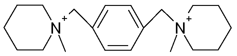
- the essential part of the additives according to the present invention is the gemini ammonium compound of the general formula la:
- ammonium compounds according to formula la are also referred to as "gemini additives" or “gemini surfactants”.
- n may be an integer from 1 to 5.
- n is an integer from 1 to 3, most preferably n is 1 .
- n may be an integer from 1 up to 10000, In this case, preferably n may be an integer from 1 to 1000, more preferably from 1 to 100, even more preferably from 1 to 20, even more preferably from 1 to 3, and most preferably 1 , provided that, if at least one Q is present, n includes all repeating units of branches Q.
- X may be a divalent group, for each repeating unit 1 to n independently selected from a linear or branched Ci to C20 alkanediyl, which may optionally be substituted and which may optionally be interrupted by up to 5 heteroatoms selected from O and N.
- the linear or branched Ci to C20 alkanediyl may be selected from an unsubstituted linear or branched Ci to C20 alkanediyl.
- X is selected from a C2 to C16 alkanediyi, more preferably a C3-C12 alkanediyi, most preferably a C 4 - C10 alkanediyi.
- X is a linear alkanediyi.
- X is selected from alkanediyi groups having the general formula III: wherein the index q is an integer of from 1 to 20, preferably 2 to 16 and most preferably 4 to 10 Most preferably, butane-1 ,4-diyl, hexane-1 ,6-diyl, or octane-1 ,8-diyl is used.
- X is X 3 -0-X 4 , with X 3 and X 4 being a linear or branched Ci C9 alkanediyi. Most preferably, X is selected from alkanediyi groups being interrupted by an oxygen atom of formula IV:
- X may be selected from a C5 to C20 cycloalkanediyl, which may optionally be substituted and which may optionally be interrupted by up to 5 heteroatoms selected from O and N.
- cycloalkanediyl may be selected from single-ring cycloalkanes, such as but not limited to hexadecane, multi-ring cycloalkanes such as but not limited to bicyclohexyl, or poly-cyclic cycloalkanes like spiro alkanes, such as but not limited to spiro [4.4]nonane, orbridged-ring alkanes.
- X may be selected from a Ce to C20 organic group of formula -X 1 -A-X 2 -, wherein X 1 and X 2 are independently selected from a Ci to C7 linear or branched alkanediyi and A is selected from a C5 to C12 aromatic moiety or a C5 to C30 cycloalkanediyl, which H atoms may optionally be substituted and which C atoms may optionally be interrupted by up to 5 heteroatoms selected from O and N.
- arylalkanediyi X 1 and X 2 may independently be selected from methanediyl, ethanediyl, propanediyl and butanediyl.
- arylalkanediyi A is selected from benzene, anthracene, biphenyl, and naphthalene. Most preferably the arylalkanediyi is 1 ,4-xylenediyl.
- X may be selected from a polyoxyalkylene diradical of formula II:
- R 5 is selected from H and a linear or branched Ci to C20 alkyl group.
- r is an integer of from 1 to 50, more preferably of from 1 to 20, most preferably of from 1 to 10.
- R 5 is selected from H and a linear or branched Ci to Ce alkyl group, more preferably R 5 is H, methyl, ethyl or propyl.
- R 1 and R 2 are monovalent groups independently selected from H, linear or branched Ci to C20 alkyl, C5 to C20 cycloalkyl, C5 to C20 aryl, Ce to C20 alkylaryl, Ce to C20 arylalkyl, Ci to C2o hydroxyalkyl, which may optionally be further substituted. Such further substituents may preferably be hydroxyl, carboxy, carbonyl, amino, amido, sulphonamide, sulphonate, and phosphate. Most preferably R 1 and R 2 are unsubstituted or substituted by one or more hydroxy or amino groups. R 1 and R 2 may generally be identical or different.
- R 1 and R 2 are unsubstituted.
- R 1 and R 2 are independently selected from Ci to C16 alkyl, more preferably C1-C12 alkyl, more preferably C1-C10 alkyl, most preferably methyl, ethyl, propyl or butyl.
- R 1 and R 2 are linear alkyl.
- Such alkyl may optionally be substituted by hydroxy (- OH), carboxy (CO-OH or its salts), amine (NH 2 ), amide (-CO-NH2), sulphonamide (-SO2-NH2), sulphonate (-SO2OH or its salts), sulphate (-OSO2OH or its salts) , phosphonate (-PO(OH)2 or its salts) and phosphate (-0-PO(OH)2, or its salts).
- a substitution is particularly useful in the use in cleaning compositions.
- At least one of R 1 and R 2 is selected from C2 to C16 hydroxyalkyl, more preferable a C2-C12 hydroxyalkyl, and most preferably a C2-C3 hydroxyalkyl. In yet another preferred embodiment at least one of R 1 and R 2 is selected from formula V
- R 8 is, for each repeating unit u independently, selected from H and linear or branched Ci to C2 alkyl, and R 10 is selected from hydroxy (-OH), carboxy (- CO-OH or its salts), amine (-NH2), amide (-CO-NH2), sulphonamide (-SO2-NH2), sulphonate (- SO2OH or its salts), sulphate (-OSO2OH or its salts) , phosphonate (-PO(OH) 2 or its salts) and phosphate (-0-PO(OH)2, or its salts).
- u is an integer of from 4 to 50, more preferably of from 9 to 40, most preferably of from 19 to 30.
- R 8 is selected from H and methyl.
- R 10 is preferably selected from hydroxy, sulphonate, sulphate and phosphate.
- at least one of R 1 and R 2 is selected from oxyethylene or oxypropylene homo or copolymers, which are terminated by groups R 8 .
- Such copolymers may have random, block, alternating or gradient structure.
- R 1 is H and R 2 is selected from linear or branched Ci to C20 alkyl, C5 to C20 cycloalkyl, C5 to C20 aryl, Ce to C20 alkylaryl, Ce to C20 arylalkyl, Ci to C20 hydroxyalkyl, which may optionally be further substituted.
- R 2 is independently selected from a Ci to C16 alkyl, more preferably a C1-C12 alkyl, more preferably a C1-C10 alkyl, most preferably methyl, ethyl, propyl or butyl.
- R 1 and R 2 are linear alkyl.
- R 3 and R 4 are monovalent groups independently selected from a linear or branched C5 to C30 alkyl group, a C5 to C30 cycloalkyl, a Ci to C20 hydroxyalkyl, and a C2 to C 4
- polyoxyalkylene Such polyoxyalkylene may be a homopolymer or a copolymer. Copolymers may be random, bock, alternating or gradient copolymers.
- the polyoxyalkylene group are chosen from compounds of formula V above, all of which may optionally be substituted, and wherein pair-wise R 3 - R 4 and adjacent R 4 - R 4 and R 3 - R 3 may optionally together form a bivalent group X as defined above, and may also be a continuation Q of the molecule by branching, and, if n is equal to or greater than 2, R 3 , R 4 or R 3 and R 4 may also be hydrogen atoms.
- R 3 and R 4 are selected from formula VI
- X 3 is selected from a chemical bond and a linear or branched, preferably linear, Ci to C 4 alkanediyl, most preferably methanediyl.
- R 5 is selected from OH, H and a linear or branched C1-C5 alkyl, preferably methyl or OH
- R 6 is selected from H and a linear or branched Ci to C20 alkyl, a Ci to C20 cycloalkyl, a Ci to C20 aryl, Ci to C20 alkylaryl and Ci to C20 arylalkyl.
- R 7 is selected from H and linear or branched Ci to C10 alkyl, preferably methyl or tert. butyl.
- R 6 is -(CH2) m -R 7 , wherein
- R 7 is selected from a Ci to C20 alkyl
- n is an integer of from 1 to 10, preferably from 2 to 6, most preferably from 2 to 4
- R 3 and R 4 are independently selected from formula VII
- R 20 is selected from OH and H
- R 21 is selected from H or Ci to C10 alkyl
- v is an integer of from 1 to 10, preferably from 1 to 6, most preferably from 2 to 4.
- the C2-C 4 polyoxyalkylene groups are preferably selected from the group consisting of homopolymers and copolymers of ethyleneoxide, propyleneoxide, butyleneoxide and styrene oxide, most preferably homopolymers and copolymers of ethyleneoxide and propyleneoxide.
- the groups R 3 and R 4 consisting of polyoxyalkylene groups may have hydroxy groups as the terminal group. However, the terminal hydroxy groups or a part of the terminal hydroxy groups may be esterified by polybasic acids, preferably sulfuric acid and/or phosphoric acid, thereby obtaining anionic and/or potentially anionic groups, preferably sulphate and/or phosphate ester groups.
- the aforementioned cations may be used as the counterions for such anionic groups.
- R 3 and R 4 each belonging to the same N center may pair-wise together form a bivalent group X selected from butanediyl, pentanediyl, and hexanediyl. Furthermore, adjacent R 4 - R 4 and R 3 - R 3 may optionally together form a bivalent group X as defined above. Structures like
- R 3 and R 4 may individually form a continuation Q of the molecule by branching.
- n is equal to or greater than 2
- R 3 , R 4 or R 3 and R 4 may be hydrogen atoms.
- any type of organic or inorganic anion Z customary and known in the field of quaternary ammonium salts may be used as counter-ion for the cation of the general formula I.
- Z is an anion ⁇ ⁇ - with x being selected from 1 , 2, 3 or 4, preferably 1 or 2.
- suitable counter-ions are selected from hydroxide, chloride, bromide, nitrate, sulphate, monomethyl sulphate, formate, acetate and propionate ions without limiting the invention thereto.
- monomethyl sulphate, sulphate or chloride is used as counter-ion.
- they can contain the aforementioned anionic counter-ions.
- hydroxide is the preferred counter-anion.
- the preferred counter-anions are selected from chloride, bromide, nitrate, sulphate, monomethyl sulphate, formate, acetate and propionate .
- Z may also be a cation. In this case non-metal cations are preferred.
- R 1 , R 2 are methyl, R 3 and R 4 together form a pentanediyl diradical in order to form a Ce cyclic moiety with the N atom;
- X is 1 ,4-xylenediyl:
- chloride counter-ion may be exchange by any other counter-ion described above.
- R 1 , R 2 are methyl, R 3 and R 4 together form a butanediyl diradical in order to form a Ce cyclic moiety with the N atom;
- X is butanediyl:
- the sulphate counter-ion may be exchange by any other counter-ion described above.
- chloride counter-ion may be exchange by any other counter-ion described above.
- R 1 is methyl
- R 2 is benzyl
- two pairs of R 3 and R 4 together form a group X
- X is ethanediyl
- the monomethyl sulphate and chloride counter-ions may be exchange by any other counter-ion described above.
- R 1 is H
- R 2 is methyl
- two pairs of R 3 and R 4 together form a group X
- X is ethanediyl
- hydroxide counter-ions may be exchange by any other counter-ion described above.
- R 1 R 2 , R 3 and R 4 are methyl and X is propanediyl:
- sulphate counter-ions may be exchange by any other counter-ion described above.
- gemini additives are those of formula I, wherein:
- X is linear or branched Ci to C10 alkyl, preferably n-pentyl or n-hexyl,
- R 1 and R 2 are selected from Ci to Ce alkyl, preferably methyl or ethyl,
- R 3 is selected from formula IV or -(C2H4-0) X -H,
- R 4 is selected from formula IV or -(C2H 4 -0) X -S0 3 - x is an integer from 10 to 40, preferably from 20 to 30.
- the concentration of the gemini additives in the aqueous rinse solution primarily depends on the critical micelle concentration value (CMC value). Therefore, the concentration can vary broadly and, therefore, can be adapted most advantageously to the particular requirements of a given method of the invention.
- the concentration is in the range of about 0.00005 to about 5% by weight, preferably about 0.0002 to about 2% by weight and, more preferably about 0.0005 to about 0.05, most preferably about 0.001 to about 0.01 % by weight, the weight percentages being based on the complete weight of the solution.
- the concentration of the gemini additives in the developer solution are typically in the range of about 1.0 ⁇ 10 -5 to about 1.5 N (based on ammonium groups or corresponding hydroxide), preferably about 1.0 - 10 "4 to about 1.0 N, more preferably about 1 .0 - 10 "3 to about 0.8 N, most preferably about 0.05 to about 0.7 N.
- the aqueous solution may contain water-miscible polar organic solvents. Examples of suitable solvents are described in US 2008/0280230 A, page 2, paragraph [0016]. Most preferably, the aqueous solution does not contain any organic solvents.
- additives may be present in the cleaning solution according to the present invention. Such additives may be
- buffers tris-hydroxymethyl-aminomethane, most preferable sodium free buffer systems.
- One or more further surfactants either non-ionic or cationic to improve surface tension and wetting capabilities.
- the aqueous solution comprising the gemini additives may be used for different purposes and objects.
- it may be used as an immersion liquid for immersing photoresists during irradiation with actinic light through a mask, as a developer solution for photoresist layers exposed to actinic radiation through a mask and as a chemical rinse solution for rinsing the patterned material layers.
- the method for manufacturing integrated circuit devices, optical devices, micromachines and mechanical precision devices has been found, the said method comprising the steps of
- the aqueous solution is removed from the contact with the substrate.
- Any known methods customarily used for removing liquids from solid surfaces can be employed.
- the solution S is removed by spin drying or drying processes making use of the Marangoni effect.
- the substrate is provided by photolithographic process comprising the steps of providing the substrate with an immersion photoresist, EUV photoresist or eBeam photoresist layer; exposing the photoresist layer to actinic radiation through a mask with or without an immersion liquid; developing the exposed photoresist layer with a developer solution to obtain a pattern having line-space dimensions of 50 nm and less, in particular, of 32 nm and less and, most especially, of 22 nm and less and an aspect ratio above 2, preferably above 10, even more preferably 50 and, most preferably, up to 75; applying a chemical rinse solution to the developed patterned photoresist layer; and (v) drying the semiconductor substrate after the application of the chemical rinse, solution preferably by spin drying or drying processes making use of the Marangoni effect.
- any customary and known positive or negative immersion photoresist, EUV photoresist or eBeam photoresist can be used.
- the immersion photoresist may already contain at least one fluorine-free cationic, anionic or amphoteric surfactant A.
- the immersion photoresist can contain nonionic surfactants. Suitable nonionic surfactants are described, for example, in US 2008/0299487 A1 , page 6, paragraph [0078].
- the immersion photoresist is a positive resist.
- UV radiation of the wavelength of 193 nm is used as the actinic radiation.
- the immersion liquid contains at least one fluorine-free cationic, amphoteric or zwitterionic gemini additive.
- any customary and known developing composition can be used for developing the exposed photoresist layer.
- developing compositions may comprise further additives.
- aqueous developer solutions containing tetraalkylammonium hydroxides, such as but not limited to tetramethylammonium hydroxide (TMAH) are used.
- the aqueous developer solutions contain at least one cationic, anionic, amphoteric or zwitterionic gemini additive.
- the chemical rinse solutions are aqueous solutions.
- the chemical rinse solutions are applied to the exposed and developed photoresist layers as puddles.
- the immersion solution, the developer solution or the chemical rinse solution contains at least one ionic gemini additive.
- the at least one cationic, anionic or amphoteric or zwitterionic gemini additive is contained in the chemical rinse solution.
- Customary and known equipment customarily used in the semiconductor industry can be used for carrying out the photolithographic process in accordance with the method of the invention. Without wishing to be bound by any theory, it is believed that the positive or negative electrical charge of the surface of the patterned layered materials causes a mutual electrostatic repulsion of neighbouring surfaces which prevents pattern collapse, as illustrated by Figure 1.
- Fig. 1 illustrates how the photoresist structures or a high aspect ratio stacks 2 are drawn
- Fig. 2 shows the result of a rinse treatment of photoresist Line-Space structures by using gemini surfactant A1 according to example 1.
- Fig. 3 shows the result of a rinse treatment of photoresist Line-Space structures by using gemini surfactant A2 according to example 2.
- Fig. 4 shows the result of a photoresist development treatment by using utra pure water
- the space between the photoresist lines was 80 nm.
- Silicon wafers were provided with 100 nm thick layers of an immersion photoresist.
- the photoresist layers were exposed to UV radiation of a wavelength of 193 through a mask using ultrapure water as the immersion liquid. Thereafter, the exposed photoresist layers were baked and developed with an aqueous developer solution containing tetramethylammonium hydroxide (TMAH).
- TMAH tetramethylammonium hydroxide
- the baked and developed photoresist layers were subjected to a chemical rinse treatment using a chemical rinse solution containing 0.002% by weight of surfactant (A1 ).
- the chemical rinse solution was applied on the wafer as a puddle. Thereafter, the silicon wafers were spun dry.
- Fig. 2 shows the respective height profile measured by AFM after the rinse treatment by using gemini surfactant A1.
- the dried patterned photoresist layers having patterns with line-space dimensions of 40 nm and an aspect ratio of about 2.5 did not show any pattern collapse.
- Example 1 was repeated except that gemini surfactant A2 was used instead of gemini surfactant A1 in the chemical rinse solution.
- Fig. 3 shows the respective height profile measured by AFM after the rinse treatment by using gemini surfactant A2.
- the dried patterned photoresist layers having photoresist line-width dimensions of 40 nm and an aspect ratio of about 2.5 did not show any pattern collapse.
- Example 1 was repeated except that ultra pure water without any additive was used in the chemical rinse solution.
- Fig. 4 shows the result of a photoresist development treatment by using ultra pure water without any additive.
- the dried patterned photoresist layers having photoresist line-width dimensions of 40 nm and an aspect ratio of about 2.5 showed significantly increased pattern collapse compared to the rinse according to examples 1 and 2.
Abstract
Description


Claims


Priority Applications (10)
| Application Number | Priority Date | Filing Date | Title |
|---|---|---|---|
| RU2015104112A RU2015104112A (en) | 2012-07-10 | 2013-07-01 | COMPOSITIONS FOR PROCESSING PREVENTING COLLAPSE OF THE DRAWING OF ELEMENTS OF THE SCHEME INCLUDING DIMERIC ADDITIVES |
| JP2015521102A JP6324955B2 (en) | 2012-07-10 | 2013-07-01 | Composition for anti-pattern disintegration treatment containing gemini additive |
| EP17195200.5A EP3299891B1 (en) | 2012-07-10 | 2013-07-01 | Use of compositions comprising gemini additives for treating semiconductor substrates |
| KR1020157003355A KR102107367B1 (en) | 2012-07-10 | 2013-07-01 | Compositions for anti pattern collapse treatment comprising gemini additives |
| US14/412,737 US10385295B2 (en) | 2012-07-10 | 2013-07-01 | Compositions for anti pattern collapse treatment comprising gemini additives |
| MYPI2015000032A MY184912A (en) | 2012-07-10 | 2013-07-01 | Compositions for anti pattern collapse treatment comprising gemini additives |
| SG11201500098XA SG11201500098XA (en) | 2012-07-10 | 2013-07-01 | Compositions for anti pattern collapse treatment comprising gemini additives |
| CN201380035822.7A CN104428716B (en) | 2012-07-10 | 2013-07-01 | The composition comprising double type additive for the processing of anti-pattern from damage |
| EP13816602.0A EP2872948B1 (en) | 2012-07-10 | 2013-07-01 | Compositions for anti pattern collapse treatment comprising gemini additives |
| IL236408A IL236408B (en) | 2012-07-10 | 2014-12-23 | Compositions for anti pattern collapse treatment comprising gemini additives |
Applications Claiming Priority (2)
| Application Number | Priority Date | Filing Date | Title |
|---|---|---|---|
| US201261669686P | 2012-07-10 | 2012-07-10 | |
| US61/669686 | 2012-07-10 |
Publications (1)
| Publication Number | Publication Date |
|---|---|
| WO2014009847A1 true WO2014009847A1 (en) | 2014-01-16 |
Family
ID=49915473
Family Applications (1)
| Application Number | Title | Priority Date | Filing Date |
|---|---|---|---|
| PCT/IB2013/055392 WO2014009847A1 (en) | 2012-07-10 | 2013-07-01 | Compositions for anti pattern collapse treatment comprising gemini additives |
Country Status (11)
| Country | Link |
|---|---|
| US (1) | US10385295B2 (en) |
| EP (2) | EP3299891B1 (en) |
| JP (1) | JP6324955B2 (en) |
| KR (1) | KR102107367B1 (en) |
| CN (1) | CN104428716B (en) |
| IL (1) | IL236408B (en) |
| MY (1) | MY184912A (en) |
| RU (1) | RU2015104112A (en) |
| SG (1) | SG11201500098XA (en) |
| TW (1) | TWI611274B (en) |
| WO (1) | WO2014009847A1 (en) |
Cited By (2)
| Publication number | Priority date | Publication date | Assignee | Title |
|---|---|---|---|---|
| JP2015168680A (en) * | 2014-03-11 | 2015-09-28 | 東ソー株式会社 | Gemini type surfactant |
| JP2016126182A (en) * | 2015-01-05 | 2016-07-11 | 信越化学工業株式会社 | Developer and pattern forming method using the same |
Families Citing this family (2)
| Publication number | Priority date | Publication date | Assignee | Title |
|---|---|---|---|---|
| JP2016139774A (en) * | 2015-01-23 | 2016-08-04 | 富士フイルム株式会社 | Pattern processing method, manufacturing method of semiconductor substrate product, and pretreatment liquid of pattern structure |
| JP2019195998A (en) * | 2018-05-08 | 2019-11-14 | 日本化薬株式会社 | Cleaning liquid and method of cleaning ink-jet printer |
Citations (2)
| Publication number | Priority date | Publication date | Assignee | Title |
|---|---|---|---|---|
| JP2009237169A (en) * | 2008-03-26 | 2009-10-15 | Fujifilm Corp | Method of making planographic printing plate |
| CN101766973A (en) * | 2009-01-07 | 2010-07-07 | 湖北大学 | Symmetric cationic surfactant and preparation method thereof |
Family Cites Families (18)
| Publication number | Priority date | Publication date | Assignee | Title |
|---|---|---|---|---|
| JP4027494B2 (en) * | 1998-04-07 | 2007-12-26 | 花王株式会社 | Rinse composition |
| US7129199B2 (en) | 2002-08-12 | 2006-10-31 | Air Products And Chemicals, Inc. | Process solutions containing surfactants |
| TW558736B (en) | 2000-02-26 | 2003-10-21 | Shipley Co Llc | Method of reducing defects |
| US20050164903A1 (en) * | 2001-08-03 | 2005-07-28 | Ki-Hwan Ko | Complexed surfactant system |
| KR20030012692A (en) * | 2001-08-03 | 2003-02-12 | 주식회사 엘지생활건강 | Surfactant system |
| US6641986B1 (en) | 2002-08-12 | 2003-11-04 | Air Products And Chemicals, Inc. | Acetylenic diol surfactant solutions and methods of using same |
| US7700257B2 (en) * | 2003-03-28 | 2010-04-20 | Tokyo Ohka Kogyo Co., Ltd. | Photoresist composition and resist pattern formation method by the use thereof |
| US20040259371A1 (en) * | 2003-06-18 | 2004-12-23 | Zhijian Lu | Reduction of resist defects |
| US20050158672A1 (en) | 2003-12-22 | 2005-07-21 | Matsushita Electric Industrial Co., Ltd. | Pattern formation method |
| KR100574349B1 (en) * | 2004-02-03 | 2006-04-27 | 삼성전자주식회사 | Cleaning solution composition and cleaning method of semiconductor device using the same |
| US20080299487A1 (en) | 2007-05-31 | 2008-12-04 | Taiwan Semiconductor Manufacturing Company, Ltd. | Lithography material and lithography process |
| CN101236357B (en) * | 2007-01-30 | 2012-07-04 | 住友化学株式会社 | Chemically amplified corrosion-resisitng agent composition |
| US20080280230A1 (en) | 2007-05-10 | 2008-11-13 | Taiwan Semiconductor Manufacturing Company, Ltd. | Photolithography process including a chemical rinse |
| JP2009237168A (en) * | 2008-03-26 | 2009-10-15 | Fujifilm Corp | Method of making planographic printing plate |
| JP5624753B2 (en) | 2009-03-31 | 2014-11-12 | 東京応化工業株式会社 | Lithographic cleaning liquid and resist pattern forming method using the same |
| MY161218A (en) | 2011-01-25 | 2017-04-14 | Basf Se | Use of surfactants having at least three short-chain perfluorinated groups rf for manufacturing integrated circuits having patterns with line-space dimensions below 50nm |
| EP2686737A4 (en) | 2011-03-18 | 2014-09-03 | Basf Se | Method for manufacturing integrated circuit devices, optical devices, micromachines and mechanical precision devices having patterned material layers with line-space dimensions of 50 nm and less |
| MY181266A (en) * | 2012-12-14 | 2020-12-21 | Basf Se | Use of compositions comprising a surfactant and a hydrophobizer for avoiding anti pattern collapse when treating patterned materials with line-space dimensions of 50 nm or below |
-
2013
- 2013-07-01 SG SG11201500098XA patent/SG11201500098XA/en unknown
- 2013-07-01 KR KR1020157003355A patent/KR102107367B1/en active IP Right Grant
- 2013-07-01 RU RU2015104112A patent/RU2015104112A/en not_active Application Discontinuation
- 2013-07-01 EP EP17195200.5A patent/EP3299891B1/en active Active
- 2013-07-01 JP JP2015521102A patent/JP6324955B2/en active Active
- 2013-07-01 EP EP13816602.0A patent/EP2872948B1/en active Active
- 2013-07-01 WO PCT/IB2013/055392 patent/WO2014009847A1/en active Application Filing
- 2013-07-01 US US14/412,737 patent/US10385295B2/en active Active
- 2013-07-01 CN CN201380035822.7A patent/CN104428716B/en active Active
- 2013-07-01 MY MYPI2015000032A patent/MY184912A/en unknown
- 2013-07-08 TW TW102124316A patent/TWI611274B/en active
-
2014
- 2014-12-23 IL IL236408A patent/IL236408B/en active IP Right Grant
Patent Citations (2)
| Publication number | Priority date | Publication date | Assignee | Title |
|---|---|---|---|---|
| JP2009237169A (en) * | 2008-03-26 | 2009-10-15 | Fujifilm Corp | Method of making planographic printing plate |
| CN101766973A (en) * | 2009-01-07 | 2010-07-07 | 湖北大学 | Symmetric cationic surfactant and preparation method thereof |
Non-Patent Citations (1)
| Title |
|---|
| See also references of EP2872948A4 * |
Cited By (2)
| Publication number | Priority date | Publication date | Assignee | Title |
|---|---|---|---|---|
| JP2015168680A (en) * | 2014-03-11 | 2015-09-28 | 東ソー株式会社 | Gemini type surfactant |
| JP2016126182A (en) * | 2015-01-05 | 2016-07-11 | 信越化学工業株式会社 | Developer and pattern forming method using the same |
Also Published As
| Publication number | Publication date |
|---|---|
| EP2872948A4 (en) | 2016-11-02 |
| EP3299891A1 (en) | 2018-03-28 |
| TWI611274B (en) | 2018-01-11 |
| EP3299891B1 (en) | 2019-05-15 |
| TW201418910A (en) | 2014-05-16 |
| KR102107367B1 (en) | 2020-05-07 |
| SG11201500098XA (en) | 2015-02-27 |
| RU2015104112A (en) | 2016-08-27 |
| US20150159123A1 (en) | 2015-06-11 |
| CN104428716A (en) | 2015-03-18 |
| EP2872948B1 (en) | 2017-10-11 |
| US10385295B2 (en) | 2019-08-20 |
| JP6324955B2 (en) | 2018-05-16 |
| JP2015529840A (en) | 2015-10-08 |
| MY184912A (en) | 2021-04-30 |
| KR20150036461A (en) | 2015-04-07 |
| IL236408A0 (en) | 2015-02-26 |
| EP2872948A1 (en) | 2015-05-20 |
| CN104428716B (en) | 2019-06-14 |
| IL236408B (en) | 2020-03-31 |
Similar Documents
| Publication | Publication Date | Title |
|---|---|---|
| EP2932525B1 (en) | Use of compositions comprising a surfactant and a hydrophobizer for avoiding anti pattern collapse when treating patterned materials with line-space dimensions of 50 nm or below | |
| TWI772552B (en) | Use of compositions comprising a siloxane-type additive for avoiding pattern collapse when treating patterned materials with line-space dimensions of 50 nm or below | |
| US9184057B2 (en) | Method for manufacturing integrated circuit devices, optical devices, micromachines and mechanical precision devices having patterned material layers with line-space dimensions of 50 nm and less | |
| EP3299891B1 (en) | Use of compositions comprising gemini additives for treating semiconductor substrates | |
| US20210198602A1 (en) | Use of compositions comprising a solvent mixture for avoiding pattern collapse when treating patterned materials with line-space dimensions of 50 nm or below | |
| KR102107370B1 (en) | Composition for manufacturing integrated circuit devices, optical devices, micromachines and mechanical precision devices | |
| EP3956729A1 (en) | Composition for avoiding pattern collapse when treating patterned materials with line-space dimensions of 50 nm or below comprising a boron-type additive | |
| EP2500777A1 (en) | Method for manufacturing integrated circuit devices, optical devices, micromachines and mechanical precision devices having patterned material layers with line-space dimensions of 50 nm and less |
Legal Events
| Date | Code | Title | Description |
|---|---|---|---|
| 121 | Ep: the epo has been informed by wipo that ep was designated in this application |
Ref document number: 13816602 Country of ref document: EP Kind code of ref document: A1 |
|
| REEP | Request for entry into the european phase |
Ref document number: 2013816602 Country of ref document: EP |
|
| WWE | Wipo information: entry into national phase |
Ref document number: 2013816602 Country of ref document: EP |
|
| WWE | Wipo information: entry into national phase |
Ref document number: 14412737 Country of ref document: US |
|
| NENP | Non-entry into the national phase |
Ref country code: DE |
|
| ENP | Entry into the national phase |
Ref document number: 2015521102 Country of ref document: JP Kind code of ref document: A |
|
| ENP | Entry into the national phase |
Ref document number: 20157003355 Country of ref document: KR Kind code of ref document: A |
|
| ENP | Entry into the national phase |
Ref document number: 2015104112 Country of ref document: RU Kind code of ref document: A |