JP6324955B2 - Composition for anti-pattern disintegration treatment containing gemini additive - Google Patents
Composition for anti-pattern disintegration treatment containing gemini additive Download PDFInfo
- Publication number
- JP6324955B2 JP6324955B2 JP2015521102A JP2015521102A JP6324955B2 JP 6324955 B2 JP6324955 B2 JP 6324955B2 JP 2015521102 A JP2015521102 A JP 2015521102A JP 2015521102 A JP2015521102 A JP 2015521102A JP 6324955 B2 JP6324955 B2 JP 6324955B2
- Authority
- JP
- Japan
- Prior art keywords
- branched
- linear
- photoresist
- alkyl
- integer
- Prior art date
- Legal status (The legal status is an assumption and is not a legal conclusion. Google has not performed a legal analysis and makes no representation as to the accuracy of the status listed.)
- Active
Links
- 239000000654 additive Substances 0.000 title claims description 36
- 239000000203 mixture Substances 0.000 title claims description 35
- 230000000996 additive effect Effects 0.000 title claims description 24
- 229920002120 photoresistant polymer Polymers 0.000 claims description 101
- 238000000034 method Methods 0.000 claims description 51
- 239000000243 solution Substances 0.000 claims description 40
- 239000000758 substrate Substances 0.000 claims description 40
- 239000000463 material Substances 0.000 claims description 34
- 125000000217 alkyl group Chemical group 0.000 claims description 31
- -1 hexane-1,6-diyl Chemical group 0.000 claims description 25
- 238000007654 immersion Methods 0.000 claims description 21
- 239000000126 substance Substances 0.000 claims description 21
- 238000004140 cleaning Methods 0.000 claims description 20
- 238000000206 photolithography Methods 0.000 claims description 20
- 230000008569 process Effects 0.000 claims description 18
- 239000004094 surface-active agent Substances 0.000 claims description 18
- 230000007547 defect Effects 0.000 claims description 16
- 238000004519 manufacturing process Methods 0.000 claims description 16
- 239000007788 liquid Substances 0.000 claims description 15
- 230000005855 radiation Effects 0.000 claims description 15
- 150000003839 salts Chemical class 0.000 claims description 15
- 125000002496 methyl group Chemical group [H]C([H])([H])* 0.000 claims description 14
- 125000003118 aryl group Chemical group 0.000 claims description 13
- 229920001577 copolymer Polymers 0.000 claims description 13
- 229910052757 nitrogen Inorganic materials 0.000 claims description 13
- 239000004065 semiconductor Substances 0.000 claims description 13
- 125000000753 cycloalkyl group Chemical group 0.000 claims description 12
- 125000005842 heteroatom Chemical group 0.000 claims description 12
- 125000002768 hydroxyalkyl group Chemical group 0.000 claims description 12
- 229910052760 oxygen Inorganic materials 0.000 claims description 12
- 238000011161 development Methods 0.000 claims description 11
- 229920001519 homopolymer Polymers 0.000 claims description 11
- 150000002500 ions Chemical class 0.000 claims description 10
- QAOWNCQODCNURD-UHFFFAOYSA-L Sulfate Chemical compound [O-]S([O-])(=O)=O QAOWNCQODCNURD-UHFFFAOYSA-L 0.000 claims description 9
- 239000007864 aqueous solution Substances 0.000 claims description 9
- 238000001035 drying Methods 0.000 claims description 8
- 125000002887 hydroxy group Chemical group [H]O* 0.000 claims description 8
- 230000003287 optical effect Effects 0.000 claims description 8
- 125000002877 alkyl aryl group Chemical group 0.000 claims description 7
- 125000006737 (C6-C20) arylalkyl group Chemical group 0.000 claims description 6
- UHOVQNZJYSORNB-UHFFFAOYSA-N Benzene Chemical compound C1=CC=CC=C1 UHOVQNZJYSORNB-UHFFFAOYSA-N 0.000 claims description 6
- 125000004435 hydrogen atom Chemical group [H]* 0.000 claims description 6
- 125000005702 oxyalkylene group Chemical group 0.000 claims description 6
- 229910019142 PO4 Inorganic materials 0.000 claims description 5
- 150000001412 amines Chemical class 0.000 claims description 5
- 239000003989 dielectric material Substances 0.000 claims description 5
- 239000002245 particle Substances 0.000 claims description 5
- 239000010452 phosphate Substances 0.000 claims description 5
- MWPLVEDNUUSJAV-UHFFFAOYSA-N anthracene Chemical compound C1=CC=CC2=CC3=CC=CC=C3C=C21 MWPLVEDNUUSJAV-UHFFFAOYSA-N 0.000 claims description 4
- 230000004888 barrier function Effects 0.000 claims description 4
- 125000004432 carbon atom Chemical group C* 0.000 claims description 4
- 125000000962 organic group Chemical group 0.000 claims description 4
- NBIIXXVUZAFLBC-UHFFFAOYSA-K phosphate Chemical compound [O-]P([O-])([O-])=O NBIIXXVUZAFLBC-UHFFFAOYSA-K 0.000 claims description 4
- 229940124530 sulfonamide Drugs 0.000 claims description 4
- 150000003456 sulfonamides Chemical class 0.000 claims description 4
- 150000001408 amides Chemical class 0.000 claims description 3
- 125000004429 atom Chemical group 0.000 claims description 3
- 125000003178 carboxy group Chemical group [H]OC(*)=O 0.000 claims description 3
- 238000010894 electron beam technology Methods 0.000 claims description 3
- 125000001570 methylene group Chemical group [H]C([H])([*:1])[*:2] 0.000 claims description 3
- UEZVMMHDMIWARA-UHFFFAOYSA-M phosphonate Chemical compound [O-]P(=O)=O UEZVMMHDMIWARA-UHFFFAOYSA-M 0.000 claims description 3
- 125000003710 aryl alkyl group Chemical group 0.000 claims description 2
- 125000000999 tert-butyl group Chemical group [H]C([H])([H])C(*)(C([H])([H])[H])C([H])([H])[H] 0.000 claims description 2
- 230000010354 integration Effects 0.000 claims 3
- 150000003460 sulfonic acids Chemical class 0.000 claims 1
- XLYOFNOQVPJJNP-UHFFFAOYSA-N water Substances O XLYOFNOQVPJJNP-UHFFFAOYSA-N 0.000 description 13
- WGTYBPLFGIVFAS-UHFFFAOYSA-M tetramethylammonium hydroxide Chemical compound [OH-].C[N+](C)(C)C WGTYBPLFGIVFAS-UHFFFAOYSA-M 0.000 description 12
- VYPSYNLAJGMNEJ-UHFFFAOYSA-N Silicium dioxide Chemical compound O=[Si]=O VYPSYNLAJGMNEJ-UHFFFAOYSA-N 0.000 description 11
- 229910021642 ultra pure water Inorganic materials 0.000 description 10
- 239000012498 ultrapure water Substances 0.000 description 10
- 229910052710 silicon Inorganic materials 0.000 description 9
- XUIMIQQOPSSXEZ-UHFFFAOYSA-N Silicon Chemical compound [Si] XUIMIQQOPSSXEZ-UHFFFAOYSA-N 0.000 description 8
- 230000009467 reduction Effects 0.000 description 8
- 239000010703 silicon Substances 0.000 description 8
- 125000000129 anionic group Chemical group 0.000 description 7
- 125000002091 cationic group Chemical group 0.000 description 6
- 235000012239 silicon dioxide Nutrition 0.000 description 6
- VEXZGXHMUGYJMC-UHFFFAOYSA-M Chloride anion Chemical compound [Cl-] VEXZGXHMUGYJMC-UHFFFAOYSA-M 0.000 description 5
- 239000000872 buffer Substances 0.000 description 5
- 239000008367 deionised water Substances 0.000 description 5
- 229910021641 deionized water Inorganic materials 0.000 description 5
- 125000001495 ethyl group Chemical group [H]C([H])([H])C([H])([H])* 0.000 description 5
- 238000000671 immersion lithography Methods 0.000 description 5
- 239000000377 silicon dioxide Substances 0.000 description 5
- 150000001768 cations Chemical class 0.000 description 4
- 230000000052 comparative effect Effects 0.000 description 4
- 239000012530 fluid Substances 0.000 description 4
- 229910052750 molybdenum Inorganic materials 0.000 description 4
- 239000002904 solvent Substances 0.000 description 4
- ZOKXTWBITQBERF-UHFFFAOYSA-N Molybdenum Chemical compound [Mo] ZOKXTWBITQBERF-UHFFFAOYSA-N 0.000 description 3
- GOOHAUXETOMSMM-UHFFFAOYSA-N Propylene oxide Chemical group CC1CO1 GOOHAUXETOMSMM-UHFFFAOYSA-N 0.000 description 3
- QAOWNCQODCNURD-UHFFFAOYSA-N Sulfuric acid Chemical compound OS(O)(=O)=O QAOWNCQODCNURD-UHFFFAOYSA-N 0.000 description 3
- 150000003868 ammonium compounds Chemical class 0.000 description 3
- 239000003093 cationic surfactant Substances 0.000 description 3
- 238000000576 coating method Methods 0.000 description 3
- 150000001875 compounds Chemical class 0.000 description 3
- 150000001924 cycloalkanes Chemical class 0.000 description 3
- 238000005516 engineering process Methods 0.000 description 3
- 238000001900 extreme ultraviolet lithography Methods 0.000 description 3
- XLYOFNOQVPJJNP-UHFFFAOYSA-M hydroxide Chemical compound [OH-] XLYOFNOQVPJJNP-UHFFFAOYSA-M 0.000 description 3
- JZMJDSHXVKJFKW-UHFFFAOYSA-M methyl sulfate(1-) Chemical compound COS([O-])(=O)=O JZMJDSHXVKJFKW-UHFFFAOYSA-M 0.000 description 3
- 239000011733 molybdenum Substances 0.000 description 3
- 125000004433 nitrogen atom Chemical group N* 0.000 description 3
- 239000002736 nonionic surfactant Substances 0.000 description 3
- 238000000059 patterning Methods 0.000 description 3
- 229910021420 polycrystalline silicon Inorganic materials 0.000 description 3
- 229920005591 polysilicon Polymers 0.000 description 3
- 238000012545 processing Methods 0.000 description 3
- 125000001436 propyl group Chemical group [H]C([*])([H])C([H])([H])C([H])([H])[H] 0.000 description 3
- BDHFUVZGWQCTTF-UHFFFAOYSA-M sulfonate Chemical compound [O-]S(=O)=O BDHFUVZGWQCTTF-UHFFFAOYSA-M 0.000 description 3
- 230000008961 swelling Effects 0.000 description 3
- QGZKDVFQNNGYKY-UHFFFAOYSA-N Ammonia Chemical compound N QGZKDVFQNNGYKY-UHFFFAOYSA-N 0.000 description 2
- IJGRMHOSHXDMSA-UHFFFAOYSA-N Atomic nitrogen Chemical compound N#N IJGRMHOSHXDMSA-UHFFFAOYSA-N 0.000 description 2
- VYZAMTAEIAYCRO-UHFFFAOYSA-N Chromium Chemical compound [Cr] VYZAMTAEIAYCRO-UHFFFAOYSA-N 0.000 description 2
- IAYPIBMASNFSPL-UHFFFAOYSA-N Ethylene oxide Chemical compound C1CO1 IAYPIBMASNFSPL-UHFFFAOYSA-N 0.000 description 2
- UFWIBTONFRDIAS-UHFFFAOYSA-N Naphthalene Chemical compound C1=CC=CC2=CC=CC=C21 UFWIBTONFRDIAS-UHFFFAOYSA-N 0.000 description 2
- NBIIXXVUZAFLBC-UHFFFAOYSA-N Phosphoric acid Chemical compound OP(O)(O)=O NBIIXXVUZAFLBC-UHFFFAOYSA-N 0.000 description 2
- NRTOMJZYCJJWKI-UHFFFAOYSA-N Titanium nitride Chemical compound [Ti]#N NRTOMJZYCJJWKI-UHFFFAOYSA-N 0.000 description 2
- 150000001335 aliphatic alkanes Chemical class 0.000 description 2
- 239000003945 anionic surfactant Substances 0.000 description 2
- 150000001450 anions Chemical class 0.000 description 2
- 238000013459 approach Methods 0.000 description 2
- 125000000484 butyl group Chemical group [H]C([*])([H])C([H])([H])C([H])([H])C([H])([H])[H] 0.000 description 2
- 239000011248 coating agent Substances 0.000 description 2
- ZUOUZKKEUPVFJK-UHFFFAOYSA-N diphenyl Chemical compound C1=CC=CC=C1C1=CC=CC=C1 ZUOUZKKEUPVFJK-UHFFFAOYSA-N 0.000 description 2
- 230000000694 effects Effects 0.000 description 2
- 238000001704 evaporation Methods 0.000 description 2
- 239000011521 glass Substances 0.000 description 2
- 238000009499 grossing Methods 0.000 description 2
- DCAYPVUWAIABOU-UHFFFAOYSA-N hexadecane Chemical compound CCCCCCCCCCCCCCCC DCAYPVUWAIABOU-UHFFFAOYSA-N 0.000 description 2
- 230000002209 hydrophobic effect Effects 0.000 description 2
- 238000001459 lithography Methods 0.000 description 2
- 239000000693 micelle Substances 0.000 description 2
- 239000003495 polar organic solvent Substances 0.000 description 2
- 229920000642 polymer Polymers 0.000 description 2
- 230000002265 prevention Effects 0.000 description 2
- 125000001424 substituent group Chemical group 0.000 description 2
- 150000003467 sulfuric acid derivatives Chemical class 0.000 description 2
- 230000003746 surface roughness Effects 0.000 description 2
- 229910052715 tantalum Inorganic materials 0.000 description 2
- GUVRBAGPIYLISA-UHFFFAOYSA-N tantalum atom Chemical compound [Ta] GUVRBAGPIYLISA-UHFFFAOYSA-N 0.000 description 2
- MZLGASXMSKOWSE-UHFFFAOYSA-N tantalum nitride Chemical compound [Ta]#N MZLGASXMSKOWSE-UHFFFAOYSA-N 0.000 description 2
- 150000005622 tetraalkylammonium hydroxides Chemical class 0.000 description 2
- 125000000008 (C1-C10) alkyl group Chemical group 0.000 description 1
- 125000004169 (C1-C6) alkyl group Chemical group 0.000 description 1
- QTBSBXVTEAMEQO-UHFFFAOYSA-M Acetate Chemical compound CC([O-])=O QTBSBXVTEAMEQO-UHFFFAOYSA-M 0.000 description 1
- CPELXLSAUQHCOX-UHFFFAOYSA-M Bromide Chemical compound [Br-] CPELXLSAUQHCOX-UHFFFAOYSA-M 0.000 description 1
- PAMIQIKDUOTOBW-UHFFFAOYSA-O C[NH+]1CCCCC1 Chemical compound C[NH+]1CCCCC1 PAMIQIKDUOTOBW-UHFFFAOYSA-O 0.000 description 1
- BDAGIHXWWSANSR-UHFFFAOYSA-M Formate Chemical compound [O-]C=O BDAGIHXWWSANSR-UHFFFAOYSA-M 0.000 description 1
- 229920000028 Gradient copolymer Polymers 0.000 description 1
- OAKJQQAXSVQMHS-UHFFFAOYSA-N Hydrazine Chemical compound NN OAKJQQAXSVQMHS-UHFFFAOYSA-N 0.000 description 1
- 229910002651 NO3 Inorganic materials 0.000 description 1
- NHNBFGGVMKEFGY-UHFFFAOYSA-N Nitrate Chemical compound [O-][N+]([O-])=O NHNBFGGVMKEFGY-UHFFFAOYSA-N 0.000 description 1
- BHHGXPLMPWCGHP-UHFFFAOYSA-N Phenethylamine Chemical compound NCCC1=CC=CC=C1 BHHGXPLMPWCGHP-UHFFFAOYSA-N 0.000 description 1
- XBDQKXXYIPTUBI-UHFFFAOYSA-M Propionate Chemical compound CCC([O-])=O XBDQKXXYIPTUBI-UHFFFAOYSA-M 0.000 description 1
- KJTLSVCANCCWHF-UHFFFAOYSA-N Ruthenium Chemical compound [Ru] KJTLSVCANCCWHF-UHFFFAOYSA-N 0.000 description 1
- AWMVMTVKBNGEAK-UHFFFAOYSA-N Styrene oxide Chemical compound C1OC1C1=CC=CC=C1 AWMVMTVKBNGEAK-UHFFFAOYSA-N 0.000 description 1
- 229910004535 TaBN Inorganic materials 0.000 description 1
- WYURNTSHIVDZCO-UHFFFAOYSA-N Tetrahydrofuran Chemical compound C1CCOC1 WYURNTSHIVDZCO-UHFFFAOYSA-N 0.000 description 1
- 239000006096 absorbing agent Substances 0.000 description 1
- 150000001242 acetic acid derivatives Chemical class 0.000 description 1
- 230000009471 action Effects 0.000 description 1
- 150000001298 alcohols Chemical class 0.000 description 1
- 229920005603 alternating copolymer Polymers 0.000 description 1
- 229910000147 aluminium phosphate Inorganic materials 0.000 description 1
- 125000003277 amino group Chemical group 0.000 description 1
- 229910021529 ammonia Inorganic materials 0.000 description 1
- QGZKDVFQNNGYKY-UHFFFAOYSA-O ammonium group Chemical group [NH4+] QGZKDVFQNNGYKY-UHFFFAOYSA-O 0.000 description 1
- 239000002280 amphoteric surfactant Substances 0.000 description 1
- 150000001449 anionic compounds Chemical class 0.000 description 1
- 238000005452 bending Methods 0.000 description 1
- 229960000686 benzalkonium chloride Drugs 0.000 description 1
- 125000001797 benzyl group Chemical group [H]C1=C([H])C([H])=C(C([H])=C1[H])C([H])([H])* 0.000 description 1
- CADWTSSKOVRVJC-UHFFFAOYSA-N benzyl(dimethyl)azanium;chloride Chemical compound [Cl-].C[NH+](C)CC1=CC=CC=C1 CADWTSSKOVRVJC-UHFFFAOYSA-N 0.000 description 1
- YOUGRGFIHBUKRS-UHFFFAOYSA-N benzyl(trimethyl)azanium Chemical compound C[N+](C)(C)CC1=CC=CC=C1 YOUGRGFIHBUKRS-UHFFFAOYSA-N 0.000 description 1
- FWLORMQUOWCQPO-UHFFFAOYSA-N benzyl-dimethyl-octadecylazanium Chemical compound CCCCCCCCCCCCCCCCCC[N+](C)(C)CC1=CC=CC=C1 FWLORMQUOWCQPO-UHFFFAOYSA-N 0.000 description 1
- 235000010290 biphenyl Nutrition 0.000 description 1
- 239000004305 biphenyl Substances 0.000 description 1
- 229920001400 block copolymer Polymers 0.000 description 1
- XTDAIYZKROTZLD-UHFFFAOYSA-N boranylidynetantalum Chemical compound [Ta]#B XTDAIYZKROTZLD-UHFFFAOYSA-N 0.000 description 1
- 150000001649 bromium compounds Chemical class 0.000 description 1
- 229910052799 carbon Inorganic materials 0.000 description 1
- 230000015556 catabolic process Effects 0.000 description 1
- RLGQACBPNDBWTB-UHFFFAOYSA-N cetyltrimethylammonium ion Chemical compound CCCCCCCCCCCCCCCC[N+](C)(C)C RLGQACBPNDBWTB-UHFFFAOYSA-N 0.000 description 1
- 238000012993 chemical processing Methods 0.000 description 1
- 239000003795 chemical substances by application Substances 0.000 description 1
- 150000001805 chlorine compounds Chemical class 0.000 description 1
- 229910052804 chromium Inorganic materials 0.000 description 1
- 239000011651 chromium Substances 0.000 description 1
- 229910052681 coesite Inorganic materials 0.000 description 1
- 229910052906 cristobalite Inorganic materials 0.000 description 1
- WVIIMZNLDWSIRH-UHFFFAOYSA-N cyclohexylcyclohexane Chemical group C1CCCCC1C1CCCCC1 WVIIMZNLDWSIRH-UHFFFAOYSA-N 0.000 description 1
- 238000006731 degradation reaction Methods 0.000 description 1
- 238000013461 design Methods 0.000 description 1
- 238000009792 diffusion process Methods 0.000 description 1
- OGQYPPBGSLZBEG-UHFFFAOYSA-N dimethyl(dioctadecyl)azanium Chemical compound CCCCCCCCCCCCCCCCCC[N+](C)(C)CCCCCCCCCCCCCCCCCC OGQYPPBGSLZBEG-UHFFFAOYSA-N 0.000 description 1
- 150000002009 diols Chemical class 0.000 description 1
- VICYBMUVWHJEFT-UHFFFAOYSA-N dodecyltrimethylammonium ion Chemical compound CCCCCCCCCCCC[N+](C)(C)C VICYBMUVWHJEFT-UHFFFAOYSA-N 0.000 description 1
- 238000007687 exposure technique Methods 0.000 description 1
- 150000004675 formic acid derivatives Chemical class 0.000 description 1
- 229910052733 gallium Inorganic materials 0.000 description 1
- 229910052739 hydrogen Inorganic materials 0.000 description 1
- 230000005661 hydrophobic surface Effects 0.000 description 1
- 150000004679 hydroxides Chemical class 0.000 description 1
- 239000004615 ingredient Substances 0.000 description 1
- 229910001412 inorganic anion Inorganic materials 0.000 description 1
- 230000003993 interaction Effects 0.000 description 1
- 238000002386 leaching Methods 0.000 description 1
- 229910052751 metal Inorganic materials 0.000 description 1
- 239000002184 metal Substances 0.000 description 1
- 150000002739 metals Chemical class 0.000 description 1
- JZMJDSHXVKJFKW-UHFFFAOYSA-N methyl sulfate Chemical class COS(O)(=O)=O JZMJDSHXVKJFKW-UHFFFAOYSA-N 0.000 description 1
- 125000001280 n-hexyl group Chemical group C(CCCCC)* 0.000 description 1
- OMEMQVZNTDHENJ-UHFFFAOYSA-N n-methyldodecan-1-amine Chemical compound CCCCCCCCCCCCNC OMEMQVZNTDHENJ-UHFFFAOYSA-N 0.000 description 1
- 125000000740 n-pentyl group Chemical group [H]C([H])([H])C([H])([H])C([H])([H])C([H])([H])C([H])([H])* 0.000 description 1
- 150000002823 nitrates Chemical class 0.000 description 1
- INAMEDPXUAWNKL-UHFFFAOYSA-N nonadecan-1-amine Chemical compound CCCCCCCCCCCCCCCCCCCN INAMEDPXUAWNKL-UHFFFAOYSA-N 0.000 description 1
- 229910052755 nonmetal Inorganic materials 0.000 description 1
- 150000002891 organic anions Chemical class 0.000 description 1
- 239000003960 organic solvent Substances 0.000 description 1
- 125000006353 oxyethylene group Chemical group 0.000 description 1
- 125000004430 oxygen atom Chemical group O* 0.000 description 1
- 238000010979 pH adjustment Methods 0.000 description 1
- 230000010363 phase shift Effects 0.000 description 1
- 125000003367 polycyclic group Polymers 0.000 description 1
- 150000007519 polyprotic acids Polymers 0.000 description 1
- 150000004672 propanoic acids Chemical class 0.000 description 1
- 235000019260 propionic acid Nutrition 0.000 description 1
- 239000010453 quartz Substances 0.000 description 1
- 150000003242 quaternary ammonium salts Chemical class 0.000 description 1
- 229920005604 random copolymer Polymers 0.000 description 1
- 239000012487 rinsing solution Substances 0.000 description 1
- 229910052707 ruthenium Inorganic materials 0.000 description 1
- 239000007787 solid Substances 0.000 description 1
- 125000003003 spiro group Chemical group 0.000 description 1
- PHICBFWUYUCFKS-UHFFFAOYSA-N spiro[4.4]nonane Chemical compound C1CCCC21CCCC2 PHICBFWUYUCFKS-UHFFFAOYSA-N 0.000 description 1
- 229910052682 stishovite Inorganic materials 0.000 description 1
- 125000000383 tetramethylene group Chemical group [H]C([H])([*:1])C([H])([H])C([H])([H])C([H])([H])[*:2] 0.000 description 1
- 229910052905 tridymite Inorganic materials 0.000 description 1
- PDSVZUAJOIQXRK-UHFFFAOYSA-N trimethyl(octadecyl)azanium Chemical compound CCCCCCCCCCCCCCCCCC[N+](C)(C)C PDSVZUAJOIQXRK-UHFFFAOYSA-N 0.000 description 1
- LENZDBCJOHFCAS-UHFFFAOYSA-N tris Chemical compound OCC(N)(CO)CO LENZDBCJOHFCAS-UHFFFAOYSA-N 0.000 description 1
- 238000005406 washing Methods 0.000 description 1
- 230000003313 weakening effect Effects 0.000 description 1
Images


Classifications
-
- G—PHYSICS
- G03—PHOTOGRAPHY; CINEMATOGRAPHY; ANALOGOUS TECHNIQUES USING WAVES OTHER THAN OPTICAL WAVES; ELECTROGRAPHY; HOLOGRAPHY
- G03F—PHOTOMECHANICAL PRODUCTION OF TEXTURED OR PATTERNED SURFACES, e.g. FOR PRINTING, FOR PROCESSING OF SEMICONDUCTOR DEVICES; MATERIALS THEREFOR; ORIGINALS THEREFOR; APPARATUS SPECIALLY ADAPTED THEREFOR
- G03F7/00—Photomechanical, e.g. photolithographic, production of textured or patterned surfaces, e.g. printing surfaces; Materials therefor, e.g. comprising photoresists; Apparatus specially adapted therefor
- G03F7/26—Processing photosensitive materials; Apparatus therefor
- G03F7/30—Imagewise removal using liquid means
- G03F7/32—Liquid compositions therefor, e.g. developers
-
- C—CHEMISTRY; METALLURGY
- C11—ANIMAL OR VEGETABLE OILS, FATS, FATTY SUBSTANCES OR WAXES; FATTY ACIDS THEREFROM; DETERGENTS; CANDLES
- C11D—DETERGENT COMPOSITIONS; USE OF SINGLE SUBSTANCES AS DETERGENTS; SOAP OR SOAP-MAKING; RESIN SOAPS; RECOVERY OF GLYCEROL
- C11D1/00—Detergent compositions based essentially on surface-active compounds; Use of these compounds as a detergent
- C11D1/008—Polymeric surface-active agents
-
- C—CHEMISTRY; METALLURGY
- C11—ANIMAL OR VEGETABLE OILS, FATS, FATTY SUBSTANCES OR WAXES; FATTY ACIDS THEREFROM; DETERGENTS; CANDLES
- C11D—DETERGENT COMPOSITIONS; USE OF SINGLE SUBSTANCES AS DETERGENTS; SOAP OR SOAP-MAKING; RESIN SOAPS; RECOVERY OF GLYCEROL
- C11D1/00—Detergent compositions based essentially on surface-active compounds; Use of these compounds as a detergent
- C11D1/38—Cationic compounds
- C11D1/40—Monoamines or polyamines; Salts thereof
-
- C—CHEMISTRY; METALLURGY
- C11—ANIMAL OR VEGETABLE OILS, FATS, FATTY SUBSTANCES OR WAXES; FATTY ACIDS THEREFROM; DETERGENTS; CANDLES
- C11D—DETERGENT COMPOSITIONS; USE OF SINGLE SUBSTANCES AS DETERGENTS; SOAP OR SOAP-MAKING; RESIN SOAPS; RECOVERY OF GLYCEROL
- C11D1/00—Detergent compositions based essentially on surface-active compounds; Use of these compounds as a detergent
- C11D1/38—Cationic compounds
- C11D1/62—Quaternary ammonium compounds
-
- G—PHYSICS
- G03—PHOTOGRAPHY; CINEMATOGRAPHY; ANALOGOUS TECHNIQUES USING WAVES OTHER THAN OPTICAL WAVES; ELECTROGRAPHY; HOLOGRAPHY
- G03F—PHOTOMECHANICAL PRODUCTION OF TEXTURED OR PATTERNED SURFACES, e.g. FOR PRINTING, FOR PROCESSING OF SEMICONDUCTOR DEVICES; MATERIALS THEREFOR; ORIGINALS THEREFOR; APPARATUS SPECIALLY ADAPTED THEREFOR
- G03F7/00—Photomechanical, e.g. photolithographic, production of textured or patterned surfaces, e.g. printing surfaces; Materials therefor, e.g. comprising photoresists; Apparatus specially adapted therefor
- G03F7/20—Exposure; Apparatus therefor
- G03F7/2041—Exposure; Apparatus therefor in the presence of a fluid, e.g. immersion; using fluid cooling means
-
- G—PHYSICS
- G03—PHOTOGRAPHY; CINEMATOGRAPHY; ANALOGOUS TECHNIQUES USING WAVES OTHER THAN OPTICAL WAVES; ELECTROGRAPHY; HOLOGRAPHY
- G03F—PHOTOMECHANICAL PRODUCTION OF TEXTURED OR PATTERNED SURFACES, e.g. FOR PRINTING, FOR PROCESSING OF SEMICONDUCTOR DEVICES; MATERIALS THEREFOR; ORIGINALS THEREFOR; APPARATUS SPECIALLY ADAPTED THEREFOR
- G03F7/00—Photomechanical, e.g. photolithographic, production of textured or patterned surfaces, e.g. printing surfaces; Materials therefor, e.g. comprising photoresists; Apparatus specially adapted therefor
- G03F7/26—Processing photosensitive materials; Apparatus therefor
- G03F7/30—Imagewise removal using liquid means
- G03F7/32—Liquid compositions therefor, e.g. developers
- G03F7/322—Aqueous alkaline compositions
-
- G—PHYSICS
- G03—PHOTOGRAPHY; CINEMATOGRAPHY; ANALOGOUS TECHNIQUES USING WAVES OTHER THAN OPTICAL WAVES; ELECTROGRAPHY; HOLOGRAPHY
- G03F—PHOTOMECHANICAL PRODUCTION OF TEXTURED OR PATTERNED SURFACES, e.g. FOR PRINTING, FOR PROCESSING OF SEMICONDUCTOR DEVICES; MATERIALS THEREFOR; ORIGINALS THEREFOR; APPARATUS SPECIALLY ADAPTED THEREFOR
- G03F7/00—Photomechanical, e.g. photolithographic, production of textured or patterned surfaces, e.g. printing surfaces; Materials therefor, e.g. comprising photoresists; Apparatus specially adapted therefor
- G03F7/26—Processing photosensitive materials; Apparatus therefor
- G03F7/40—Treatment after imagewise removal, e.g. baking
-
- H—ELECTRICITY
- H01—ELECTRIC ELEMENTS
- H01L—SEMICONDUCTOR DEVICES NOT COVERED BY CLASS H10
- H01L21/00—Processes or apparatus adapted for the manufacture or treatment of semiconductor or solid state devices or of parts thereof
- H01L21/02—Manufacture or treatment of semiconductor devices or of parts thereof
- H01L21/027—Making masks on semiconductor bodies for further photolithographic processing not provided for in group H01L21/18 or H01L21/34
- H01L21/0271—Making masks on semiconductor bodies for further photolithographic processing not provided for in group H01L21/18 or H01L21/34 comprising organic layers
- H01L21/0273—Making masks on semiconductor bodies for further photolithographic processing not provided for in group H01L21/18 or H01L21/34 comprising organic layers characterised by the treatment of photoresist layers
- H01L21/0274—Photolithographic processes
-
- C11D2111/22—
Description
本発明は、特に集積回路デバイス、光学デバイス、マイクロマシン及び機械的精度デバイスを製造するための方法において、特に抗パターン(anti pattern)の崩壊を回避するフォトレジストを現像する工程、及びポストエッチ残留物除去のために有用な組成物に関する。 The present invention relates to a process for developing a photoresist that avoids particularly anti-pattern collapse, and a post-etch residue, particularly in methods for manufacturing integrated circuit devices, optical devices, micromachines and mechanical precision devices. It relates to a composition useful for removal.
LSI、VLSI、及びULSIを製造する方法において、パターニングされたフォトレジスト層のようなパターニングされた材料層、窒化チタン、タンタル又は窒化タンタルを含む、又はそれらからなるパターニングされたバリア材料層、例えば交互のポリシリコン及び二酸化ケイ素層等の積み重ねを含む、又はそれらからなるパターニングされたマルチスタック材料層、及び二酸化ケイ素又は低誘電率(low-k)、超低誘電率(ultra-low-k)の誘電材料を含む、又はそれらからなるパターニングされた誘電材料層が、フォトリソグラフィ技術によって製造される。最近では、そのようなパターニングされた材料層は、高アスペクト比で、実に22nmより低い寸法の構造を含む。 In a method of manufacturing LSI, VLSI and ULSI, a patterned barrier material layer, eg, alternating, comprising or consisting of a patterned material layer such as a patterned photoresist layer, titanium nitride, tantalum or tantalum nitride A patterned multi-stack material layer comprising or consisting of a stack of polysilicon and silicon dioxide layers, and silicon dioxide or low dielectric constant (low-k), ultra-low dielectric constant (ultra-low-k) A patterned dielectric material layer comprising or consisting of a dielectric material is produced by photolithography techniques. Recently, such patterned material layers include structures with high aspect ratios, indeed below 22 nm.
フォトリソグラフィは、マスク上のパターンが半導体ウエハーのような基板上へ投影される方法である。半導体フォトリソグラフィは、通常、半導体基板の頂面上へフォトレジストの層を塗布する工程、及びフォトレジストを、マスクを介して、化学線、特に、例えば193nmの波長のUV線に露光する工程を含む。193nmのフォトリソグラフィを22nm及び15nmの技術ノードへ広げるため、液浸フォトリソグラフィ(immersion photolithography)が、分解能向上技術として開発されている。この技術において、光学システムの最終レンズ及びフォトレジスト表面の間に空隙(air gap)が、1より大きい屈折率を有する液体媒体、例えば193nmの波長で1.44の屈折率を有する超純水等に置き換えられる。しかしながら、浸出、水の取り込み及びパターン劣化を回避するため、バリアコーティング、又は耐水フォトレジストを使用しなければならない。しかしながら、これらの手段は、製造工程の煩雑さを追加し、そのために不利である。 Photolithography is a method in which a pattern on a mask is projected onto a substrate such as a semiconductor wafer. Semiconductor photolithography usually involves a step of applying a layer of photoresist onto the top surface of a semiconductor substrate, and a step of exposing the photoresist to actinic radiation, particularly UV radiation having a wavelength of, for example, 193 nm through a mask. Including. In order to extend 193 nm photolithography to 22 nm and 15 nm technology nodes, immersion photolithography has been developed as a resolution enhancement technique. In this technique, a liquid medium in which the air gap between the final lens of the optical system and the photoresist surface has a refractive index greater than 1, such as ultrapure water having a refractive index of 1.44 at a wavelength of 193 nm. Is replaced by However, barrier coatings or water resistant photoresists must be used to avoid leaching, water uptake and pattern degradation. However, these means add to the complexity of the manufacturing process and are therefore disadvantageous.
193nmの液浸リソグラフィの他に、有意により短い波長の照射技術が、20nm以下の印刷形状になるように、さらなるダウンスケールの必要性を実現させる解決策であると考えられている。電子線(e-Beam)の他、約13.5nmの波長での極紫外線(Extreme Ultraviolet) (EUV)リソグラフィは、将来、液浸リソグラフィの後を継ぐ最も有望な候補であると思われる。露光の後、続くプロセスフローは、液浸及びEUVリソグラフィに関して非常に類似している。 In addition to 193 nm immersion lithography, significantly shorter wavelength irradiation techniques are considered to be a solution that realizes the need for further downscaling so that print shapes of 20 nm or less are achieved. In addition to the electron beam (e-Beam), Extreme Ultraviolet (EUV) lithography at a wavelength of about 13.5 nm appears to be the most promising candidate to succeed the immersion lithography in the future. After exposure, the subsequent process flow is very similar for immersion and EUV lithography.
任意の露光後ベイク(post-exposure bake)(PEB)は、露光したフォトレジストポリマーを開裂することができるようによく行なわれる。その後、開裂されたポリマーフォトレジスト含む基板は、水性現像組成物に可溶性である、露光したフォトレジストを除去するために現像チャンバーへ移される。通常、そのような現像組成物は、限定されないが、水酸化テトラメチルアンモニウム(TMAH)等の水酸化テトラアルキルアンモニウムを含み、露光したフォトレジストを現像するため、パドル(puddle)状にレジスト表面へ塗布される。その後、溶解したフォトレジストのポリマーを除去するため、脱イオン水すすぎ液が基板へ塗布される。次いで、基板は、スピン乾燥プロセスへ送られる。その後、基板は、フォトレジスト表面から水分を全て除去するハードベイクプロセスを含み得る次のプロセスへ送られ得る。 Optional post-exposure bake (PEB) is often performed so that the exposed photoresist polymer can be cleaved. Thereafter, the substrate containing the cleaved polymer photoresist is transferred to a development chamber to remove the exposed photoresist that is soluble in the aqueous developer composition. Such developer compositions typically include, but are not limited to, tetraalkylammonium hydroxide, such as tetramethylammonium hydroxide (TMAH), and are exposed to the resist surface in a puddle form to develop the exposed photoresist. Applied. Thereafter, a deionized water rinse is applied to the substrate to remove the dissolved photoresist polymer. The substrate is then sent to a spin drying process. The substrate can then be sent to the next process, which can include a hard bake process that removes all moisture from the photoresist surface.
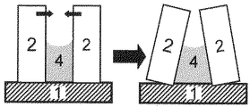
しかしながら、露光技術に関わりなく、小さいパターンの湿式化学処理は、複数の問題を伴う。技術が進歩し、寸法要求がますます厳しくなるにつれて、フォトレジストパターンは、比較的薄く、且つ高い構造又は特徴、すなわち基板上に、高いアスペクト比を有する特徴を含むことが要求される。これらの構造は、特に、化学的すすぎプロセス、及びスピン乾燥プロセスから残存し、隣接したフォトレジスト特徴間に付いたすすぎ液脱イオン水の液体又は溶液の過度の毛細管力のため、スピン乾燥プロセス中に、折り曲げ及び/又は崩壊(いわゆる崩壊)を被り得る。毛細管力により引き起こされる小さい特徴間の計算される最大応力σは、Namatsuら、Appl. Phys.Lett.66(20),1995年に従い、以下の通り:

説明され得る。
However, regardless of the exposure technique, small pattern wet chemical processing involves several problems. As technology advances and dimensional requirements become increasingly demanding, photoresist patterns are required to be relatively thin and include high structures or features, i.e., features with high aspect ratios on the substrate. These structures remain in particular during the spin drying process due to the excessive capillary force of the liquid or solution of the rinse liquid deionized water that survives the chemical rinse process and the spin dry process and that is between adjacent photoresist features. Can undergo bending and / or collapse (so-called collapse). The calculated maximum stress σ between small features caused by capillary forces is described in Namatsu et al., Appl. Phys. Lett. 66 (20), 1995, as follows:
Can be explained.
最大応力を低くするためには、一般に、以下のアプローチがある:
(a)流体の表面張力γを低くする、
(b)特徴材料表面上の流体の接触角を低くする。
In general, there are the following approaches to lower the maximum stress:
(A) reducing the surface tension γ of the fluid;
(B) Lowering the contact angle of the fluid on the feature material surface.
液浸リソグラフィについて最大応力を低くするための別のアプローチでは、より疎水性にするための変性ポリマーを有するフォトレジストを使用することを含み得る。しかしながら、この溶液は現像剤溶液の湿潤性を低下させ得る。 Another approach to lower maximum stress for immersion lithography may involve using a photoresist with a modified polymer to make it more hydrophobic. However, this solution can reduce the wettability of the developer solution.
従来のフォトリソグラフィプロセスの別の問題は、レジスト及び光学分解能の限界に起因するラインエッジラフネス(LER)及びラインワイズラフネス(LWR)である。LERは、特徴の理想型からの水平及び垂直偏差を含む。特に、限界寸法が縮小するにつれて、LER及びLWSが、より問題になり、ICデバイスの製造プロセスにおける歩留まり損失を引き起こし得る。 Another problem with conventional photolithography processes is line edge roughness (LER) and line width roughness (LWR) due to resist and optical resolution limitations. LER includes horizontal and vertical deviations from the ideal type of feature. In particular, as critical dimensions shrink, LER and LWS become more problematic and can cause yield loss in the IC device manufacturing process.
寸法の収縮に起因して、欠陥低減を達成するため、粒子の除去もまた重要な要因となる。これはフォトレジストパターンだけではなく、光学デバイス、マイクロマシン、及び機械的精度デバイスの製造中に発生する他のパターニングされた材料層にも適用する。 Due to dimensional shrinkage, particle removal is also an important factor to achieve defect reduction. This applies not only to photoresist patterns, but also to other patterned material layers that occur during the manufacture of optical devices, micromachines, and mechanical precision devices.
従来のフォトリソグラフィプロセスのさらなる問題は、ウォーターマーク欠陥が存在することである。ウォーターマークは、脱イオン水又はすすぎ液をフォトレジストの疎水性表面から振り落とすことができないときに、フォトレジスト上に生じ得る。フォトレジストは、特に分離した、又は疎の(non-dense)パターニングの領域で疎水性であり得る。ウォーターマークは、歩留まり、及びICデバイス性能に悪影響を有する。 A further problem with conventional photolithography processes is the presence of watermark defects. A watermark can occur on a photoresist when deionized water or a rinsing liquid cannot be sprinkled off the hydrophobic surface of the photoresist. The photoresist can be hydrophobic, especially in areas of isolated or non-dense patterning. Watermarks have a negative impact on yield and IC device performance.
しかしながら、上記のすすぎ/洗浄工程の他に、フォトレジスト現像工程におけるフォトレジストの膨張もまた、パターン崩壊の危険性を増加させ得、そのため回避されるべきである。 However, in addition to the rinsing / washing steps described above, swelling of the photoresist in the photoresist development step can also increase the risk of pattern collapse and should therefore be avoided.
EP1553454A2は、90nmのライン−スペース寸法(line-space dimension)を有するパターン用のすすぎ(rinsing)組成物中のカチオン界面活性剤として、セチルメチルアンモニウム、ステアリルメチルアンモニウム、セチルトリメチルアンモニウム、ステアリルトリメチルアンモニウム、ジステアリルジメチルアンモニウム、ステアリルジメチルベンジルアンモニウム、ドデシルメチルアンモニウム、ドデシルトリメチルアンモニウム、ベンジルメチルアンモニウム、ベンジルトリメチルアンモニウム、及び塩化ベンザルコニウムの使用を開示する。 EP 1553454 A2 is a cationic surfactant in a rinsing composition for a pattern having a line-space dimension of 90 nm as cetylmethylammonium, stearylmethylammonium, cetyltrimethylammonium, stearyltrimethylammonium, Disclosed is the use of distearyldimethylammonium, stearyldimethylbenzylammonium, dodecylmethylammonium, dodecyltrimethylammonium, benzylmethylammonium, benzyltrimethylammonium, and benzalkonium chloride.
US6670107B2は、臨界ミセル濃度以下の濃度で、カチオン性及び非イオン性界面活性剤を含む電子デバイスにおける欠陥の低減のための方法を開示する。US2010/0248164A1は、アニオン性界面活性剤、アミン及び水からなるパターン崩壊を防止するためのすすぎ溶液を開示する。 US 6670107 B2 discloses a method for the reduction of defects in electronic devices comprising cationic and nonionic surfactants at concentrations below the critical micelle concentration. US2010 / 0248164A1 discloses a rinsing solution for preventing pattern collapse consisting of an anionic surfactant, an amine and water.
特許出願US2000/53172A1は、アセチレンジオール系の界面活性剤溶液が、フォトレジスト表面を親水性にして、そのためすすぎ液又は溶液の湿潤性を改善することによってパターン崩壊を防止することを開示する。 Patent application US2000 / 53172A1 discloses that acetylenic diol-based surfactant solutions prevent pattern collapse by making the photoresist surface hydrophilic, thus improving the wettability of the rinsing liquid or solution.
要約すると、パターン崩壊は、一般に:
A.現像段階におけるフォトレジストの膨張、
B.すすぎの終わりの液体振り落とし(spin-off)の間のすすぎ/洗浄組成物の毛細管作用、
C.パターニングされた構造の下層への弱い接着、
D.膨張及び構造の弱化の原因となる材料の不適合、
によって引き起こされ得る。
In summary, pattern collapse is generally:
A. Swelling of the photoresist in the development stage,
B. The capillary action of the rinse / cleaning composition during the spin-off of the end of the rinse,
C. Weak adhesion to the underlying layer of the patterned structure,
D. Material incompatibility that causes expansion and weakening of the structure,
Can be caused by.
本発明は、主にA及びBに基づく問題、すなわち、フォトレジストの現像後の欠陥低減すすぎ液(defect reduction rinse)を使用することによってフォトレジストの膨張を防止すること、及びパターン崩壊を防止することに対処する。 The present invention primarily prevents problems based on A and B, ie, photoresist expansion by using a defect reduction rinse after development of the photoresist, and prevents pattern collapse. Deal with that.
したがって、本発明の目的は、50nm以下のノードのための、特に32nm以下のノードのための、特に22nm以下のノードのための集積回路を製造する方法であって、もはや従来技術の製造方法の不利な点を示さない方法を提供することである。 Accordingly, it is an object of the present invention to provide a method of manufacturing an integrated circuit for a node of 50 nm or less, in particular for a node of 32 nm or less, in particular for a node of 22 nm or less. It is to provide a method that does not show disadvantages.
本発明のさらなる目的は、50nm以下のノードのための、特に32nm以下のノードのための、特に22nm以下のノードのためのフォトリソグラフィ・マスクを製造する方法であって、もはや従来技術の製造方法の不利な点を示さない方法を提供することである。 A further object of the present invention is a method of manufacturing a photolithographic mask for nodes below 50 nm, in particular for nodes below 32 nm, in particular for nodes below 22 nm, which is no longer a prior art manufacturing method. It is to provide a method that does not show the disadvantages.
特に、本発明による化合物は、
高いアスペクト比、及び50nm以下、特に32nm以下、特に22nmのライン−スペース寸法を有するパターンを含む、
フォトレジスト層の液浸フォトリソグラフィ、
マスクを介して化学線で露光したフォトレジスト層の現像、
パターニングされた材料層の化学的すすぎ、
フォトリソグラフィ・マスクの化学的すすぎを、
パターン崩壊を引き起こすこと、LER、LWR及びウォーターマーク欠陥の増加なしに可能にしなければならない。
In particular, the compounds according to the invention are
Including patterns having high aspect ratios and line-space dimensions of 50 nm or less, especially 32 nm or less, especially 22 nm,
Immersion photolithography of photoresist layer,
Development of a photoresist layer exposed with actinic radiation through a mask,
Chemical rinsing of the patterned material layer,
Chemical rinsing of photolithography masks,
It must be possible to cause pattern collapse without increasing LER, LWR and watermark defects.
本発明による構成要素は、現像されたフォトレジストパターンの表面の粗さを平滑化することによって、LER及びLWRの有意な低減を可能にすべきである。本発明はまた、パターニングされた材料層上、特に、これに限定されるものではないが、フォトレジストパターン上のウォーターマーク欠陥の効果的な防止及び/又は除去を可能にすべきである。また、本発明はまた、パターニングされた材料層上の有意な欠陥低減を達成するため、効果的な粒子の除去を可能にすべきである。 Components according to the present invention should allow a significant reduction in LER and LWR by smoothing the surface roughness of the developed photoresist pattern. The present invention should also enable effective prevention and / or removal of watermark defects on the patterned material layer, particularly but not limited to, a photoresist pattern. The present invention should also allow for effective particle removal to achieve significant defect reduction on the patterned material layer.
本発明による構成要素はまた、フォトレジストの膨張の有意な低減を可能にすべきである。 Components according to the present invention should also allow a significant reduction in photoresist expansion.
本発明の第1の実施形態は、半導体基板又はフォトリソグラフィ・マスクを処理するための組成物における一般式I:
Xは、各々の繰り返し単位1〜nごとに独立して、
(a)任意に置換されていてもよく、且つ任意にO及びNから選択される5個以下のヘテロ原子で中断されていてもよい直鎖又は分岐のC1〜C20アルカンジイル、
(b)任意に置換されていてもよく、且つ任意にO及びNから選択される5個以下のヘテロ原子で中断されていてもよいC6〜C20シクロアルカンジイル、
(c)式:―X1−A−X2−;(式中、X1及びX2は、独立してC1〜C7の直鎖又は分岐のアルカンジイルから選択され、Aは、H原子が任意に置換されていてもよく、且つC原子が任意にO及びNから選択される5個以下のヘテロ原子で中断されていてもよい、C5〜C12芳香族部分、又はC5〜C30シクロアルカンジイルから選択される。)のC6〜C20有機基、
(d)式II:
のポリオキシアルキレンジラジカル、
から選択される二価の基であり、
R1及びR2は、独立してH、直鎖状若しくは分岐したC1〜C20アルキル、C5〜C20シクロアルキル、C5〜C20アリール、C6〜C20のアルキルアリール、C6〜C20アリールアルキル、C1〜C20ヒドロキシアルキル、又はC2〜C4オキシアルキレンのホモポリマー若しくはコポリマーから選択される一価の基であり、これらの全ては、任意にさらに置換されていてもよく、
R3及びR4は、独立して直鎖又は分岐のC5〜C30アルキル基、C5〜C30シクロアルキル、C1〜C20ヒドロキシアルキル、及びC2〜C4オキシアルキレンのホモポリマー又はコポリマーから選択される一価の基であり、これらの全ては、任意に置換されていてもよく、対のR3−R4及び隣接したR4−R4及びR3−R3が、任意に共に二価の基Xを形成してもよく、及び分岐による分子の連続Qであってもよく、nが2以上の場合は、R3、R4、又はR3及びR4はまた、水素原子であってもよく、
nは、1〜5の整数であるか、又はX、R3及びR4の少なくとも1種が、C2〜C4ポリオキシアルキレン基を含む場合、nは、1〜10000の整数であってもよく、ただし、少なくとも1種のQが存在する場合、nは、分岐Qの全ての繰り返し単位を含み、
Qは、
zは、界面活性剤全体で電気的に非荷電となるように選択される整数であり、
Zは、対イオン(counter-ion)である。]
で表されるジェミニ添加剤(gemini additive)の使用方法である。
A first embodiment of the present invention provides a general formula I in a composition for processing a semiconductor substrate or photolithography mask:
X is independently for each repeating unit 1-n,
(A) may be optionally substituted, and optionally C 1 -C 20 alkanediyl 5 or fewer may straight be interrupted by heteroatoms or branched selected from O and N,
(B) a C 6 -C 20 cycloalkanediyl optionally substituted and optionally interrupted by up to 5 heteroatoms selected from O and N;
(C) Formula: —X 1 —A—X 2 —; wherein X 1 and X 2 are independently selected from C 1 to C 7 linear or branched alkanediyl, and A is H A C 5 to C 12 aromatic moiety, or C 5 , in which the atoms may be optionally substituted and the C atom may be optionally interrupted by up to 5 heteroatoms selected from O and N C 6 -C 20 organic group selected from -C 30 cycloalkane-diyl.),
(D) Formula II:
A polyoxyalkylene diradical of
A divalent group selected from
R 1 and R 2 are independently H, linear or branched C 1 -C 20 alkyl, C 5 -C 20 cycloalkyl, C 5 -C 20 aryl, C 6 -C 20 alkyl aryl, C 6 -C 20 arylalkyl, C 1 -C 20 hydroxyalkyl, or C 2 -C 4 monovalent radicals selected from homopolymers or copolymers of oxyalkylene, all of which are further optionally substituted You can,
R 3 and R 4 are independently a linear or branched C 5 -C 30 alkyl group, a C 5 -C 30 cycloalkyl, a C 1 -C 20 hydroxyalkyl, and a C 2 -C 4 oxyalkylene homopolymer Or a monovalent group selected from a copolymer, all of which may be optionally substituted, wherein the pair R 3 -R 4 and the adjacent R 4 -R 4 and R 3 -R 3 are Optionally together they may form a divalent group X and may be a continuous Q of the molecule by branching, and when n is 2 or more, R 3 , R 4 , or R 3 and R 4 are also May be a hydrogen atom,
n is an integer of 1 to 5, or when at least one of X, R 3 and R 4 contains a C 2 to C 4 polyoxyalkylene group, n is an integer of 1 to 10000 Provided that, when at least one Q is present, n includes all repeating units of branch Q;
Q is
z is an integer selected to be electrically uncharged throughout the surfactant,
Z is a counter-ion. ]
It is the usage method of the gemini additive (gemini additive) represented by these.
本発明の別の実施形態によれば、集積回路デバイス、光学デバイス、マイクロマシン及び機械的精度デバイスを製造するための方法が見出されており、前記方法は、以下の工程:
(a)基板を供給する工程、
(b)前記基板にフォトレジスト層を供給する工程、
(c)前記フォトレジスト層を、浸液あり又は浸液なしで、マスクを介して化学線で露光する工程、
(d)前記基板を、少なくとも1回、フォトレジストを現像するための現像組成物と接触させ、32nm以下のライン−スペース寸法及び、2以上のアスペクト比を有するパターンを得る工程、
(e)前記基板を、少なくとも1回、水性洗浄組成物と接触させる工程、
を含み、
工程(d)の前記現像組成物、及び工程(e)の前記洗浄組成物の少なくとも1種が、ジェミニ添加剤を含む。
According to another embodiment of the present invention, a method for manufacturing integrated circuit devices, optical devices, micromachines and mechanical precision devices has been found, said method comprising the following steps:
(A) supplying a substrate;
(B) supplying a photoresist layer to the substrate;
(C) exposing the photoresist layer with actinic radiation through a mask with or without immersion liquid;
(D) contacting the substrate at least once with a developing composition for developing a photoresist to obtain a pattern having a line-space dimension of 32 nm or less and an aspect ratio of 2 or more;
(E) contacting the substrate with the aqueous cleaning composition at least once;
Including
At least one of the developing composition in step (d) and the cleaning composition in step (e) contains a gemini additive.
従来技術を考慮すると、本発明の目的が、本発明による使用又は方法によって解決され得たことは、驚くべきことであり、当業者に予期され得ないことであった。 In view of the prior art, it was surprising and unexpected to those skilled in the art that the object of the present invention could be solved by the use or method according to the present invention.
本発明によるジェミニ添加剤の使用が、フォトレジスト層の液浸フォトリソグラフィ、マスクを介して化学線で露光されたフォトレジスト層の現像、パターニングされた材料層若しくはフォトリソグラフィ・マスクの洗浄、又はそれらの組合せを可能にさせることは驚くべきことである。 The use of the gemini additive according to the present invention may include immersion photolithography of a photoresist layer, development of a photoresist layer exposed to actinic radiation through a mask, cleaning of a patterned material layer or photolithography mask, or It is surprising to allow the combination of.
本発明による界面活性剤は特に、パターン現像するため、又は50nm以下、特に32nm以下、さらに特に22nm以下のライン−スペース寸法を有するパターンを含む現像されたフォトレジスト層若しくはフォトリソグラフィ・マスクを洗浄するために有用である。 The surfactants according to the invention are particularly suitable for pattern development or for cleaning developed photoresist layers or photolithography masks containing patterns having line-space dimensions of 50 nm or less, in particular 32 nm or less, more particularly 22 nm or less. Useful for.
また、本発明によるジェミニ添加剤は特に、フォトレジスト構造については2以上、特に非フォトレジスト構造については10以上のアスペクト比のために有用であり、フォトレジストの場合のパターン崩壊、ラインエッジラフネス(LER)、ラインワイズラフネス(LWR)、ウォーターマーク欠陥を引き起こすことなく、高いアスペクト比の場合の抗パターン崩壊、欠陥低減及び洗浄のために有用である。 The gemini additive according to the present invention is also particularly useful for aspect ratios of 2 or more for photoresist structures, particularly 10 or more for non-photoresist structures. LER), line width roughness (LWR), and water mark defects, without causing pattern defects, useful for anti-pattern collapse, defect reduction and cleaning at high aspect ratios.
本発明によるジェミニ添加剤を含む組成物は一般に、フォトレジスト構造、及び高いアスペクト比(HARS、通常アスペクト比が10以上)を有する非フォトレジストパターンの抗パターン崩壊を回避するために有用であることに留意すべきである。 Compositions comprising gemini additives according to the present invention are generally useful for avoiding anti-pattern collapse of photoresist structures and non-photoresist patterns having high aspect ratios (HARS, typically aspect ratios greater than 10) Should be noted.
それどころか、本発明の方法は、現像されたフォトレジストパターンの表面の粗さを滑らかにすることによるLER及びLWRの有意な低減、フォトレジストパターン上だけでなく、他のパターニングされた材料層上のウォーターマーク欠陥の効果的な防止及び/又は除去、及び粒子の効果的な除去を可能にさせ、これによりフォトレジストパターン上だけでなく、他のパターニングされた材料層上の有意な欠陥低減が、達成され得た。 On the contrary, the method of the present invention significantly reduces LER and LWR by smoothing the surface roughness of the developed photoresist pattern, not only on the photoresist pattern, but also on other patterned material layers. Allows effective prevention and / or removal of watermark defects and effective removal of particles, thereby significantly reducing defects on other patterned material layers as well as on photoresist patterns, Could be achieved.
如何なる理論にも拘束されることなく、現像剤組成物におけるジェミニ添加剤の使用は、低減された拡散のためフォトレジスト層の膨張を防止することができたようである。このことはまた、続く工程中のフォトレジストのパターン崩壊の危険性を低減する。ジェミニ添加剤の現像剤溶液における使用は、表面張力、及び現像剤溶液とフォトレジストの相互作用を調整することを可能にする。 Without being bound by any theory, it appears that the use of gemini additives in the developer composition was able to prevent swelling of the photoresist layer due to reduced diffusion. This also reduces the risk of photoresist pattern collapse during subsequent processing. The use of gemini additives in a developer solution makes it possible to adjust the surface tension and the interaction of the developer solution with the photoresist.
一般式I:
ICデバイス、光学デバイス、マイクロマシン及び機械的精度デバイスを製造するために使用される、如何なる慣習及び公知の基板も本発明の方法に使用され得る。好ましくは、基板は半導体基板であり、さらに好ましくはシリコン−ガリウムウエハーを含むシリコンウエハーであり、ウエハーは、ICデバイス、特にLSI、CLSI及びULSIを有するICを含むICデバイスを製造するために慣習的に使用される。 Any conventional and known substrate used to fabricate IC devices, optical devices, micromachines and mechanical precision devices can be used in the method of the present invention. Preferably, the substrate is a semiconductor substrate, more preferably a silicon wafer including a silicon-gallium wafer, which is customary for manufacturing IC devices, particularly IC devices including ICs having LSI, CLSI and ULSI. Used for.
前記組成物は特に、50nm以下、特に32nm以下、及び特に22nm以下のライン−スペース寸法を有するパターニングされた材料層、すなわち、sub−22nm技術ノード用のパターニングされた材料層を有する基盤を処理するために適切である。前記パターニングされた材料層は好ましくは、2を超える比、好ましくは10を超える比、さらにいっそう好ましくは50を超える比を有する。特にパターニングされた材料層がフォトレジスト構造を含む、又はそれらからなる場合、前記比は2を超え、それらが非フォトレジスト構造を含む、又はそれらからなる場合、前記比は10を超える。最も好ましくは、前記アスペクト比は、例として、15nmフラッシュデバイス用に、75以下の範囲である。 The composition in particular treats a substrate with a patterned material layer having line-space dimensions of 50 nm or less, in particular 32 nm or less and in particular 22 nm or less, ie a patterned material layer for a sub-22 nm technology node. Is appropriate for. The patterned material layer preferably has a ratio greater than 2, preferably greater than 10, even more preferably greater than 50. In particular, if the patterned material layer comprises or consists of a photoresist structure, the ratio exceeds 2, and if they comprise or consist of a non-photoresist structure, the ratio exceeds 10. Most preferably, the aspect ratio is in the range of 75 or less, for example, for a 15 nm flash device.
以下のリソグラフィのフォトマスクの種類は、現在、そのようなライン−スペース寸法及びアスペクト比を調製するために使用され、両方ともモリブデン及びシリコン層を含む。 The following lithographic photomask types are currently used to prepare such line-space dimensions and aspect ratios, both including molybdenum and silicon layers.
(a)193nm ArFリソグラフィ(及び旧世代)において使用されたフォトマスクは、透明であり、ガラス上の不透明なモリブデン(Mo)シリコン(Si)(OMOG)フォトマスクを使用する透過型フォトマスクとして知られている。この場合、OMOGフォトマスクブランクは、限定されないが、合成水晶基板等の193nm放射線に透過性の適切な基板上に、交互のMo/Si層を被覆することにより作製される。その後、薄いクロムフィルムがこれらの層の最上部に被覆される。前記Mo/Si層及びクロム層は、ArF放射光を吸収するが、これらの層が基板のある範囲から除去されたとき、光はその範囲を通過する。この方法は、標準の位相シフトマスクよりも低いパターニングアスペクト比を可能とし、より細かいデザインノードにより適切である。この種類のリソグラフィは浸液あり又は浸液なしで使用され得る。 (A) The photomask used in 193 nm ArF lithography (and previous generations) is transparent and is known as a transmissive photomask using an opaque molybdenum (Mo) silicon (Si) (OMOG) photomask on glass. It has been. In this case, the OMOG photomask blank is made by coating alternating Mo / Si layers on a suitable substrate that is transparent to 193 nm radiation, such as, but not limited to, a synthetic quartz substrate. A thin chrome film is then coated on top of these layers. The Mo / Si layer and the chromium layer absorb ArF radiation, but when these layers are removed from an area of the substrate, the light passes through the area. This method allows for a lower patterning aspect ratio than standard phase shift masks and is more appropriate for finer design nodes. This type of lithography can be used with or without immersion.
(b)EUVLマスクは一般に、モリブデン(Mo)及びシリコン(Si)の多数の交互の層で作製され、反射型マスクとして知られている。EUV光の波長が、13.5nmであり、それはほとんど全ての物質によって吸収されるので、したがって、EUVマスクは、反射材料を使用する。これらのマスクは、ガラス基板上に反射性のMo及びSiの80以下の交互層(各々40層)を被覆することによって作製される。反射性Mo/Si層の最上部に緩衝及び吸収層が被覆され、パターニングされる。吸収層は通常、窒素と結合させたホウ化タンタル系材料(nitrogenized tantalum boride-based material)(TaBN)を含む。緩衝層は通常、SiO2製である。交互のMo/Si層に衝突するEUV光は反射され、吸収層に衝突するEUV光は吸収される。 (B) EUVL masks are generally made of a number of alternating layers of molybdenum (Mo) and silicon (Si) and are known as reflective masks. Since the wavelength of EUV light is 13.5 nm, which is absorbed by almost all substances, EUV masks therefore use reflective materials. These masks are made by coating up to 80 alternating layers (40 layers each) of reflective Mo and Si on a glass substrate. A buffer and absorber layer is coated on top of the reflective Mo / Si layer and patterned. The absorbing layer typically includes a tantalum boride-based material (TaBN) combined with nitrogen. The buffer layer is usually made of SiO2. EUV light impinging on the alternating Mo / Si layer is reflected and EUV light impinging on the absorbing layer is absorbed.
本発明による組成物は、それらの形状により崩壊の傾向がある構造である限り、如何なるパターニングされた材料の基板にも適用され得る。 The compositions according to the invention can be applied to substrates of any patterned material as long as they are structures that tend to collapse due to their shape.
例として、パターニングされた材料層は、
(a)既に放射線で露光され、現像剤溶液で現像されたフォトレジスト層
(b)ルテニウム、窒化チタン、タンタル又は窒化タンタルを含む、又はそれらからなるパターニングされたバリア材料層、
(c)シリコン、ポリシリコン、二酸化ケイ素、低誘電率及び超低誘電率材料、高誘電(high-k)材料、シリコン及びポリシリコン以外の半導体及び金属からなる群から選択される少なくとも2種の異なる材料を含む、又はそれらからなるパターニングされたマルチスタック材料層、及び
(d)二酸化ケイ素又は低誘電率若しくは超低誘電率誘電材料を含む、又はそれらからなるパターニングされた誘電材料層、
(e)例えば半導体デバイスの製造等における、任意のフォトリソグラフィプロセスに使用されるパターニングされたフォトリソグラフィ・マスク、
であり得る。
As an example, the patterned material layer is
(A) a photoresist layer that has already been exposed to radiation and developed with a developer solution; (b) a patterned barrier material layer comprising or consisting of ruthenium, titanium nitride, tantalum or tantalum nitride;
(C) at least two selected from the group consisting of silicon, polysilicon, silicon dioxide, low and ultra low dielectric constant materials, high dielectric (high-k) materials, semiconductors and metals other than silicon and polysilicon A patterned multi-stack material layer comprising or consisting of different materials, and (d) a patterned dielectric material layer comprising or consisting of silicon dioxide or a low or very low dielectric constant dielectric material,
(E) a patterned photolithography mask used in any photolithography process, eg, in the manufacture of semiconductor devices, etc.
It can be.
洗浄/すすぎ組成物、及び前記ジェミニ添加剤を含む現像剤組成物は、好ましくは水性溶液である。 The cleaning / rinsing composition and the developer composition containing the gemini additive are preferably aqueous solutions.
通常、洗浄/すすぎ組成物は、約6〜約8のpHで使用される。 Typically, the cleaning / rinsing composition is used at a pH of about 6 to about 8.
通常、現像組成物は、8以上のpHで、好ましくは9〜14のpHで使用される。 Usually, the developing composition is used at a pH of 8 or more, preferably at a pH of 9-14.
「水性」は、溶媒が主溶媒として、水、好ましくは脱イオン水、最も好ましくは超純水を含むことを意味する。前記組成物の水性の本質を台無しにしないような少量ではあるが、水性組成物は水混和性の極性有機溶媒を含み得る。溶媒は、本質的に水、好ましくは脱イオン水、最も好ましくは超純水からなることが好ましい。超純水の例は、5ppt(ng/kg)又はそれより良い濃度、5ppb(ng/g)又はそれより良いアニオン濃度、50ppb又はそれより良い全有機体含量(TOC)で、0.2mmより大きい粒子がml当たり10000未満含む。 “Aqueous” means that the solvent comprises water as the main solvent, preferably deionized water, most preferably ultrapure water. A small amount so as not to spoil the aqueous nature of the composition, but the aqueous composition may comprise a water-miscible polar organic solvent. It is preferred that the solvent consists essentially of water, preferably deionized water, most preferably ultrapure water. Examples of ultrapure water are 5ppt (ng / kg) or better concentration, 5ppb (ng / g) or better anion concentration, 50ppb or better total organic content (TOC), from 0.2mm Large particles contain less than 10,000 per ml.
本発明による添加剤の本質的な部分は、一般式Ia:
また、対イオンZは中性の根拠のために存在する必要がある。式Iaによるアンモニウム化合物は、「ジェミニ添加剤」又は「ジェミニ界面活性剤」とも称される。 Moreover, the counter ion Z needs to exist for the reason of neutrality. The ammonium compounds according to formula Ia are also referred to as “gemini additives” or “gemini surfactants”.
式Iにおいて、nは1〜5の整数であってもよい。好ましくは、nは1〜3の整数であり、最も好ましくは、nは1である。 In formula I, n may be an integer from 1 to 5. Preferably n is an integer from 1 to 3, most preferably n is 1.
しかしながら、X、R3及びR4の少なくとも1種が、オキシアルキレン又はポリオキシアルキレン基を含む場合、水中での溶解度がより高い分子量の化合物でかなり良くなり、したがって、nは1〜10000の整数であってもよく、この場合好ましくは、nは1〜1000の整数、さらに好ましくは1〜100の整数、さらにいっそう好ましくは1〜20の整数、さらにいっそう好ましくは1〜3の整数、最も好ましくは1であってもよく、ただし、少なくとも1種のQが存在する場合、nは、分岐Qの全ての繰り返し単位を含む。 However, if at least one of X, R 3 and R 4 contains an oxyalkylene or polyoxyalkylene group, it will be considerably better at a molecular weight compound with higher solubility in water, so n is an integer from 1 to 10,000 In this case, preferably, n is an integer of 1 to 1000, more preferably an integer of 1 to 100, still more preferably an integer of 1 to 20, still more preferably an integer of 1 to 3, most preferably May be 1, provided that when at least one Q is present, n includes all repeating units of branch Q.
第1の実施形態において、Xは、各々の繰り返し単位1〜nごとに独立して、任意に置換されていてもよく、且つ任意にO及びNから選択される5個以下のヘテロ原子で中断されていてもよい直鎖又は分岐のC1〜C20アルカンジイルから選択される二価の基であってもよい。好ましい実施形態において、直鎖又は分岐のC1〜C20アルカンジイルは、非置換の直鎖又は分岐のC1〜C20アルカンジイルであってもよい。さらに別の好ましい実施形態において、XはC2〜C16アルカンジイル、さらに好ましくはC3〜C12アルカンジイル、最も好ましくはC4〜C10アルカンジイルから選択される。さらに別の好ましい実施形態において、Xは直鎖状アルカンジイルである。 In a first embodiment, X is optionally substituted independently for each repeating unit 1-n and optionally interrupted by no more than 5 heteroatoms selected from O and N It may be a divalent group selected from linear or branched C 1 to C 20 alkanediyl which may be used. In a preferred embodiment, C 1 -C 20 alkanediyl linear or branched can be a C 1 -C 20 alkanediyl unsubstituted straight or branched. In yet another preferred embodiment, X is C 2 -C 16 alkanediyl, more preferably C 3 -C 12 alkanediyl, most preferably selected from C 4 -C 10 alkanediyl. In yet another preferred embodiment, X is a linear alkanediyl.
さらに好ましくは、Xは一般式III:
−(CH2)q− (III)
[式中、添字qは、1〜20の整数、好ましくは2〜16の整数、最も好ましくは4〜10の整数である。]を有するアルカンジイル基から選択される。最も好ましくは、ブタン−1,4−ジイル、ヘキサン−1,6−ジイル、又はオクタン−1,8−ジイルが使用される。
More preferably, X is of the general formula III:
- (CH 2) q - ( III)
[In the formula, the subscript q is an integer of 1 to 20, preferably an integer of 2 to 16, and most preferably an integer of 4 to 10. ] Is selected from alkanediyl groups having Most preferably, butane-1,4-diyl, hexane-1,6-diyl, or octane-1,8-diyl is used.
さらに別の好ましい実施形態において、Xは、X3−O−X4;[X3及びX4は、直鎖又は分岐のC1〜C9アルカンジイルである。]である。最も好ましくは、Xは式IV:
−(CH2)r−O−(CH2)s− (IV)
[式中、添字r及びsは、各々の添字で独立して、1〜8の整数、好ましくは2〜6の整数、最も好ましくは3〜4の整数である。]の酸素原子で中断されているアルカンジイル基から選択される。
In yet another preferred embodiment, X is, X 3 -O-X 4; [X 3 and X 4 is a linear or branched C 1 -C 9 alkanediyl. ]. Most preferably, X is of the formula IV:
- (CH 2) r -O- ( CH 2) s - (IV)
[Wherein, the subscripts r and s are each independently an integer of 1 to 8, preferably an integer of 2 to 6, and most preferably an integer of 3 to 4. Or an alkanediyl group interrupted by an oxygen atom.
第2の実施形態において、Xは、任意に置換されていてもよく、且つ任意にO及びNから選択される5個以下のヘテロ原子で中断されていてもよいC6〜C20シクロアルカンジイルから選択されてもよい。そのようなシクロアルカンジイルは、限定されないがヘキサデカン等の単環シクロアルカン、限定されないがビシクロヘキシル等の多重環(multi-ring)シクロアルカン、又は限定されないがスピロ[4.4]ノナン等のスピロアルカン、オルブリッジド環(orbridged-ring)アルカンのような多環式(poly-cyclic)シクロアルカンから選択されてもよい。 In a second embodiment, X is optionally substituted and is optionally interrupted with up to 5 heteroatoms selected from O and N C 6 -C 20 cycloalkanediyl. May be selected. Such cycloalkanediyls include, but are not limited to, monocyclic cycloalkanes such as hexadecane, multi-ring cycloalkanes such as but not limited to bicyclohexyl, or spiros such as, but not limited to spiro [4.4] nonane. Alkanes may be selected from poly-cyclic cycloalkanes such as orbridged-ring alkanes.
第3の実施形態において、Xは、式:―X1−A−X2−;[式中、X1及びX2は、独立してC1〜C7の直鎖又は分岐のアルカンジイルから選択され、Aは、H原子が任意に置換されていてもよく、且つC原子が任意にO及びNから選択される5個以下のヘテロ原子で中断されていてもよい、C5〜C12芳香族部分、又はC5〜C30シクロアルカンジイルから選択される。]のC6〜C20有機基から選択されてもよい。好ましいアリールアルカンジイルにおいて、X1及びX2は、独立してメタンジイル、エタンジイル、プロパンジイル及びブタンジイルから選択されてもよい。別の好ましいアリールアルカンジイルにおいて、Aは、ベンゼン、アントラセン、ビフェニル、及びナフタレンから選択される。最も好ましくは、アリールアルカンジイルは1,4−キシレンジイルである。 In a third embodiment, X is of the formula: —X 1 —A—X 2 —; wherein X 1 and X 2 are independently from C 1 -C 7 linear or branched alkanediyl. Selected, A may be optionally substituted with H atoms, and C atoms may be interrupted with up to 5 heteroatoms optionally selected from O and N, C 5 -C 12 aromatic moiety, or is selected from C 5 -C 30 cycloalkane diyl. ] C 6 -C 20 organic group. In preferred arylalkanediyl, X 1 and X 2 may be independently selected from methanediyl, ethanediyl, propanediyl and butanediyl. In another preferred arylalkanediyl, A is selected from benzene, anthracene, biphenyl, and naphthalene. Most preferably, the arylalkanediyl is 1,4-xylenediyl.
第4の実施形態において、Xは、式II:
式Iにおいて、R1及びR2は、独立してH、任意にさらに置換されていてもよい、直鎖又は分岐のC1〜C20アルキル、C5〜C20シクロアルキル、C5〜C20アリール、C6〜C20のアルキルアリール、C6〜C20アリールアルキル、C1〜C20ヒドロキシアルキルから選択される一価の基である。そのようなさらなる置換基は好ましくは、ヒドロキシル、カルボキシ、カルボニル、アミノ、アミド、スルホンアミド、スルホン酸塩、硫酸塩であってもよい。最も好ましくは、R1及びR2は非置換であるか、又は1個以上のヒドロキシル又はアミノ基で置換されている。R1及びR2は、一般に同一であっても、異なっていてもよい。 In Formula I, R 1 and R 2 are independently H, optionally further substituted, linear or branched C 1 -C 20 alkyl, C 5 -C 20 cycloalkyl, C 5 -C It is a monovalent group selected from 20 aryl, C 6 -C 20 alkylaryl, C 6 -C 20 arylalkyl, C 1 -C 20 hydroxyalkyl. Such further substituents may preferably be hydroxyl, carboxy, carbonyl, amino, amide, sulfonamide, sulfonate, sulfate. Most preferably, R 1 and R 2 are unsubstituted or substituted with one or more hydroxyl or amino groups. R 1 and R 2 may generally be the same or different.
第1の好ましい実施形態において、R1及びR2は非置換である。別の好ましい実施形態において、R1及びR2は、独立してC1〜C16アルキル、さらに好ましくはC1〜C12アルキル、さらに好ましくはC1〜C10、最も好ましくはメチル、エチル、プロピル又はブチルから選択される。さらに別の好ましい実施形態において、R1及びR2は、直鎖状アルキルである。そのようなアルキルは、任意にヒドロキシ(−OH)、カルボキシ(−CO−OH又はその塩)、アミン(−NH2)、アミド(−CO−NH2)、スルホンアミド(−SO2−NH2)、スルホン酸塩(−SO2OH又はその塩)、硫酸塩(−OSO2OH又はその塩)、ホスホン酸塩(−PO(OH)2又はその塩)、及びリン酸塩(−O−PO(OH)2、又はその塩)によって置換されていてもよい。置換は、洗浄組成物における使用において特に有用である。好ましい実施形態において、R1及びR2の少なくとも1種はC2〜C16ヒドロキシアルキル、さらに好ましくはC2〜C12ヒドロキシアルキル、最も好ましくはC2〜C3ヒドロキシアルキルから選択される。さらに別の好ましい実施形態において、R1及びR2の少なくとも1種は式V:
特に好ましい実施形態において、R1及びR2の少なくとも1種は、基R8によって終結されるオキシエチレン又はオキシプロピレンのホモポリマー又はコポリマーから選択される。そのようなコポリマーは、ランダム、ブロック、交互又は勾配構造を有していてもよい。 In a particularly preferred embodiment, at least one of R 1 and R 2 is selected from oxyethylene or oxypropylene homopolymers or copolymers terminated by a group R 8 . Such copolymers may have a random, block, alternating or gradient structure.
現像剤として使用されるには、R1はHであり、且つR2は、任意にさらに置換されていてもよい、直鎖又は分岐のC1〜C20アルキル、C5〜C20シクロアルキル、C5〜C20アリール、C6〜C20アルキルアリール、C6〜C20アリールアルキル、C1〜C20ヒドロキシアルキルから選択される。具体的な実施形態において、R2は、独立してC1〜C16アルキル、さらに好ましくはC1〜C12アルキル、さらに好ましくはC1〜C10アルキル、最も好ましくはメチル、エチル、プロピル又はブチルから選択される。さらに別の好ましい実施形態において、R1及びR2は直鎖状アルキルである。 To be used as a developer, R 1 is H and R 2 is optionally further substituted, linear or branched C 1 -C 20 alkyl, C 5 -C 20 cycloalkyl. , C 5 -C 20 aryl, C 6 -C 20 alkylaryl, C 6 -C 20 arylalkyl, is selected from C 1 -C 20 hydroxyalkyl. In specific embodiments, R 2 is independently C 1 -C 16 alkyl, more preferably C 1 -C 12 alkyl, more preferably C 1 -C 10 alkyl, most preferably methyl, ethyl, propyl or Selected from butyl. In yet another preferred embodiment, R 1 and R 2 are linear alkyl.
式Iにおいて、R3及びR4は、独立して直鎖又は分岐のC5〜C30アルキル基、C5〜C30シクロアルキル、C1〜C20ヒドロキシアルキル、及びC2〜C4ポリオキシアルキレンから選択される一価の基である。そのようなポリオキシアルキレンは、ホモポリマーであっても、コポリマーであってもよい。コポリマーは、ランダム、ブロック、交互又は勾配コポリマーであってもよい。好ましくは、ポリオキシアルキレン基は上記式Vの化合物から選択され、これらの全ては、任意に置換されていてもよく、対のR3−R4及び隣接したR4−R4及びR3−R3が、任意に共に上記の二価の基Xを形成してもよく、及び分岐による分子の連続Qであってもよく、nが2以上の場合は、R3、R4、又はR3及びR4はまた、水素原子であってもよい。 In Formula I, R 3 and R 4 are independently linear or branched C 5 -C 30 alkyl groups, C 5 -C 30 cycloalkyl, C 1 -C 20 hydroxyalkyl, and C 2 -C 4 poly It is a monovalent group selected from oxyalkylene. Such polyoxyalkylenes may be homopolymers or copolymers. The copolymer may be a random, block, alternating or gradient copolymer. Preferably, the polyoxyalkylene group is selected from compounds of formula V above, all of which are optionally substituted and are a pair of R 3 -R 4 and adjacent R 4 -R 4 and R 3- R 3 may optionally together form the above-mentioned divalent group X, and may be a continuous Q of the molecule by branching, and when n is 2 or more, R 3 , R 4 , or R 3 and R 4 may also be a hydrogen atom.
好ましい実施形態において、R3及びR4は式VI:
X3は、化学結合、及び直鎖又は分岐の、好ましくは直鎖状のC1〜C4のアルカンジイル、最も好ましくはメタンジイルから選択され、
R5は、OH、H、及び直鎖又は分岐のC1〜C5アルキル、好ましくはメチル又はOHから選択され、
R6は、H、及び直鎖又は分岐のC1〜C20アルキル、C1〜C20シクロアルキル、C1〜C20アリール、C1〜C20アルキルアリール、C1〜C20アリールアルキルから選択され、
R7は、H、及び直鎖又は分岐のC1〜C10アルキル、好ましくはメチル又はtert−ブチルから選択される。]
から選択される。
In a preferred embodiment, R 3 and R 4 are of formula VI:
X 3 is selected from chemical bonds and linear or branched, preferably linear C 1 -C 4 alkanediyl, most preferably methanediyl;
R 5 is selected from OH, H and linear or branched C 1 -C 5 alkyl, preferably methyl or OH;
R 6 is from H and linear or branched C 1 -C 20 alkyl, C 1 -C 20 cycloalkyl, C 1 -C 20 aryl, C 1 -C 20 alkyl aryl, C 1 -C 20 aryl alkyl Selected
R 7 is selected from H and linear or branched C 1 -C 10 alkyl, preferably methyl or tert-butyl. ]
Selected from.
別の好ましい実施形態において、R6は、−(CH2)m−R7;[式中、
R7は、C1〜C20アルキルから選択され、
mは、1〜10の整数、好ましくは2〜6の整数、最も好ましくは2〜4の整数である。]である。
In another preferred embodiment, R 6 is — (CH 2 ) m —R 7 ;
R 7 is selected from C 1 -C 20 alkyl;
m is an integer of 1 to 10, preferably an integer of 2 to 6, and most preferably an integer of 2 to 4. ].
さらなる好ましい実施形態において、R3及びR4は、独立して式VII:
前記C2〜C4ポリオキシアルキレン基は、好ましくはエチレンオキサイド、プロピレンオキサイド、ブチレンオキサイド及びスチレンオキサイドのホモポリマー及びコポリマーからなる群から、最も好ましくはエチレンオキサイド及びプロピレンオキサイドのホモポリマー又はコポリマーから習う群から選択される。 The C 2 -C 4 polyoxyalkylene group, Learning preferably ethylene oxide, propylene oxide, from the group consisting of homopolymers and copolymers of butylene oxide and styrene oxide, and most preferably from homopolymers or copolymers of ethylene oxide and propylene oxide Selected from the group.
ポリオキシアルキレン基からなる前記基R3及びR4は、末端基としてヒドロキシ基を有していてもよい。しかしながら、末端ヒドロキシ基又は末端ヒドロキシ基の一部は、多塩基酸、好ましくは硫酸及び/又はリン酸によってエステル化され、それによりアニオン性及び/又は潜在的アニオン性基、好ましくは硫酸エステル及び/又はリン酸エステル基を得ていてもよい。前述のカチオンは、そのようなアニオン性基のための対イオンとして使用されてもよい。 The groups R 3 and R 4 composed of a polyoxyalkylene group may have a hydroxy group as a terminal group. However, the terminal hydroxy group or part of the terminal hydroxy group is esterified with a polybasic acid, preferably sulfuric acid and / or phosphoric acid, so that anionic and / or potentially anionic groups, preferably sulfate esters and / or Alternatively, a phosphate ester group may be obtained. The aforementioned cations may be used as counter ions for such anionic groups.
別の好ましい実施形態において、同一のN中心に属するR3及びR4は、対で共にブタンジイル、ペンタンジイル、及びヘキサンジイルから選択される二価の基Xを形成してもよい。また、隣接したR4−R4及びR3−R3は、任意に共に上記で規定した二価の基Xを形成してもよい。このようにして、
R3及びR4は、個別に分岐による分子の連続Qを形成してもよいことは強調される必要がある。 It should be emphasized that R 3 and R 4 may individually form a continuous Q of the molecule by branching.
n化2以上である具体的な事例において、R3,R4又はR3及びR4は、水素原子であってもよい。 In a specific case where n is 2 or more, R 3 , R 4 or R 3 and R 4 may be a hydrogen atom.
第4級アンモニウム塩の分野における、慣習及び公知の如何なる種類の有機又は無機アニオンZは、一般式Iのカチオン用の対イオンとして使用されてもよい。好ましくは、Zは、アニオンZx−;(xは、1、2、3又は4から、好ましくは1又は2から選択される。)である。適切な対イオンの具体的な例としては、そのことで本発明を限定することなしに、水酸化物、塩化物、臭化物、硝酸塩、硫酸塩、モノメチル硫酸塩、ギ酸塩、酢酸塩及びプロピオン酸縁イオンから選択される。好ましくは、モノメチル硫酸塩、硫酸塩又は塩化物が、対イオンとして使用される。さらに、それらは、上述のアニオン性対イオンを含み得る。 Any kind of organic or inorganic anions Z customary and known in the field of quaternary ammonium salts may be used as counterions for cations of the general formula I. Preferably, Z is an anion Z x- ; where x is selected from 1, 2, 3 or 4, preferably 1 or 2. Specific examples of suitable counterions include, without limiting the invention, hydroxides, chlorides, bromides, nitrates, sulfates, monomethyl sulfates, formates, acetates and propionic acids Selected from edge ions. Preferably, monomethyl sulfate, sulfate or chloride is used as the counter ion. In addition, they may contain anionic counter ions as described above.
現像剤組成物に使用するために、水酸化物は、好ましい対イオンである。洗浄組成物に使用するために、好ましい対イオンは、塩化物、臭化物、硝酸塩、硫酸塩、モノメチル硫酸塩、ギ酸塩、酢酸塩及びプロピオン酸塩から選択される。負電荷の置換基が、正電荷を持つN原子を超えて、アンモニウム化合物に存在する場合、Zはまた、カチオンであってもよい。この場合、非金属カチオンが好ましい。 For use in developer compositions, hydroxide is the preferred counter ion. For use in cleaning compositions, preferred counterions are selected from chloride, bromide, nitrate, sulfate, monomethyl sulfate, formate, acetate and propionate. If a negatively charged substituent is present in the ammonium compound beyond the positively charged N atom, Z may also be a cation. In this case, non-metal cations are preferred.
本発明の具体的な実施形態において、R1、R2はメチルであり、R3及びR4は、共にN原子を有するC6環部分を形成するためにペンタンジイルジラジカルを形成し、Xは、1,4−キシレンジイルである:
この場合、塩化物対イオンは、上記の任意の他の対イオンによって交換されていてもよい。 In this case, the chloride counterion may be exchanged by any other counterion described above.
別の実施形態において、R1、R2はメチルであり、R3及びR4は、共にN原子を有するC6環部分を形成するためにブタンジイルジラジカルを形成し、Xは、ブタンジイルである:
この場合、硫酸塩対イオンは、上記の任意の他の対イオンによって交換されていてもよい。 In this case, the sulfate counterion may be exchanged by any other counterion described above.
さらに別の実施形態において、R1=R2=R3=R4はエチルであり、Xは、1,4−キシレンジイルである:
この場合、塩化物対イオンは、上記の任意の他の対イオンによって交換されていてもよい。 In this case, the chloride counterion may be exchanged by any other counterion described above.
さらに別の実施形態おいて、R1はメチルであり、R2はベンジルであり、R3及びR4の2対は、共に基Xを形成し、Xは、エタンジイルである:
この場合、モノメチル硫酸塩及び塩化物対イオンは、上記の任意の他の対イオンによって交換されていてもよい。 In this case, the monomethyl sulfate and chloride counter ions may be exchanged by any other counter ions described above.
さらに別の実施形態において、R1はHであり、R2はメチルであり、R3及びR4の2対は、共に基Xを形成し、Xは、エタンジイルである:
この場合、水酸化物対イオンは、上記の任意の他の対イオンによって交換されていてもよい。 In this case, the hydroxide counterion may be exchanged with any other counterion described above.
さらに別の実施形態において、R1、R2、R3及びR4はメチルであり、Xは、プロパンジイルである:
この場合、硫酸塩対イオンは、上記の任意の他の対イオンによって交換されていてもよい。 In this case, the sulfate counterion may be exchanged by any other counterion described above.
特に適切なジェミニ添加剤の他の例としては、式Iの式中、
Xが、直鎖又は分岐のC1〜C10アルキル、好ましくはn−ペンチル又はn−ヘキシルであり、
R1及びR2が、C1〜C6アルキル、好ましくはメチル又はエチルから選択され、
R3が、式IV、又は−(C2H4−O)x−Hから選択され、
R4が、式IV、又は−(C2H4−O)x−SO3 −から選択され、
xが、10〜40の整数、好ましくは20〜30の整数である、
ものである。
Other examples of particularly suitable gemini additives include those of formula I
X is linear or branched C1-C10 alkyl, preferably n-pentyl or n-hexyl,
R 1 and R 2 are selected from C 1 -C 6 alkyl, preferably methyl or ethyl;
R 3 is selected from formula IV, or — (C 2 H 4 —O) x —H;
R 4 is selected from formula IV, or — (C 2 H 4 —O) x —SO 3 — ,
x is an integer of 10 to 40, preferably an integer of 20 to 30;
Is.
水性すすぎ溶液中のジェミニ添加剤の濃度は、主に臨界ミセル濃度値(CMC値)に依存する。したがって、前記濃度は、広範に変化させ得、したがって、所定の本発明の方法の具体的な要求に最も有利に適合させ得る。好ましくは、前記濃度は、約0.00005〜約5質量%、好ましくは約0.0002〜約2質量%、さらに好ましくは約0.0005〜約0.05質量%、最も好ましくは約0.001〜約0.01質量%の範囲であり、質量パーセントは、溶液の全部の質量に基づいたものである。 The concentration of gemini additive in the aqueous rinse solution depends mainly on the critical micelle concentration value (CMC value). Accordingly, the concentration can vary widely and can therefore be most advantageously adapted to the specific requirements of a given inventive method. Preferably, the concentration is about 0.00005 to about 5% by weight, preferably about 0.0002 to about 2% by weight, more preferably about 0.0005 to about 0.05% by weight, and most preferably about 0.00. The range is from 001 to about 0.01% by weight, and the weight percent is based on the total weight of the solution.
現像剤溶液中のジェミニ添加剤の濃度は、通常、約1.0×10⁻⁵〜約1.5N(アンモニウム基又は対応する水酸化物に基づいて)、好ましくは約1.0×10⁻⁴〜約1.0N、さらに好ましくは約1.0×10⁻³〜約0.8N、最も好ましくは約0.05〜約0.7Nの範囲である。 The concentration of the gemini additive in the developer solution is usually about 1.0 × 10 −5 to about 1.5 N (based on ammonium groups or the corresponding hydroxide), preferably about 1.0 × 10 − 4 to about 1.0 N, more preferably about 1.0 × 10 −3 to about 0.8 N, and most preferably about 0.05 to about 0.7 N.
水性溶液は、水混和性極性有機溶媒を含んでいてもよい。適切な溶媒の例としては、US2008/0280230A、第2頁段落[0016]に記載される。最も好ましくは、水性溶液は、如何なる有機溶媒も含まない。
The aqueous solution may contain a water miscible polar organic solvent. Examples of suitable solvents are described in US 2008 / 0280230A,
さらなる添加剤が、本発明による洗浄溶液中に存在していてもよい。 Additional additives may be present in the cleaning solution according to the invention.
そのような添加剤は、
(I)一般に湿潤性を改善するためのアルコール又はアミン
(II)限定されないが、アンモニア含有緩衝剤、トリス−ヒドロキシメチル−アミノメタン、最も好ましいナトリウムを含まない緩衝系等のpH調整のための緩衝剤成分、
(III)表面張力及び湿潤性を改善するための、非イオン性或いはカチオン性の1種以上のさらなる界面活性剤、
であってもよい。
Such additives are:
(I) Alcohols or amines for generally improving wettability (II) Buffers for pH adjustment such as, but not limited to, ammonia-containing buffers, tris-hydroxymethyl-aminomethane, and most preferred sodium-free buffer systems Agent ingredients,
(III) one or more additional surfactants, nonionic or cationic, to improve surface tension and wettability,
It may be.
本発明の方法に従って、ジェミニ添加剤を含む水性溶液は種々の目的及び対象物に使用されてもよい。したがって、マスクを介して化学光で照射中のフォトレジストを液浸するための浸液として、マスクを介して化学線に露光したフォトレジスト層用の現像剤溶液として、及びパターニングされた材料層及びフォトリソグラフィ・マスクをすすぐための化学的すすぎ溶液として使用されてもよい。 In accordance with the method of the present invention, aqueous solutions containing gemini additives may be used for various purposes and objects. Therefore, as an immersion liquid for immersing the photoresist being irradiated with actinic light through the mask, as a developer solution for the photoresist layer exposed to actinic radiation through the mask, and a patterned material layer and It may be used as a chemical rinse solution for rinsing the photolithographic mask.
一実施形態において、集積回路デバイス、光学デバイス、マイクロマシン及び機械的精度デバイスを製造するための方法が見出されており、前記方法は、以下の工程:
(1)50nm以下のライン−スペース寸法及び2以上のアスペクト比を有するパターニングされた材料層を有する基板を供給する工程、
(2)前記基板を、少なくとも1回、少なくとも1種の本明細書に記載されたジェミニ添加剤を含む水性溶液と接触させる工程、及び
(3)前記基板との接触から前記水性溶液を除去する工程、
を含む。
In one embodiment, a method for manufacturing integrated circuit devices, optical devices, micromachines and mechanical precision devices has been found, said method comprising the following steps:
(1) supplying a substrate having a patterned material layer having a line-space dimension of 50 nm or less and an aspect ratio of 2 or more;
(2) contacting the substrate at least once with an aqueous solution comprising at least one gemini additive described herein; and (3) removing the aqueous solution from contact with the substrate. Process,
including.
本発明による第3の工程において、水性溶液は基板との接触から除去される。固体表面から液体を除去するために慣習的に使用される如何なる公知の方法も使用され得る。好ましくは、溶液Sは、スピン乾燥、又はマランゴニ効果を使用する乾燥プロセスによって除去される。 In the third step according to the invention, the aqueous solution is removed from contact with the substrate. Any known method conventionally used to remove liquid from a solid surface can be used. Preferably, the solution S is removed by spin drying or a drying process using the Marangoni effect.
好ましくは、本発明の方法の第1の工程において、基板は以下の工程:
(i)基板に液浸フォトレジスト層、極紫外線(EUV)フォトレジスト層、又は電子線(eBeam)フォトレジスト層を供給する工程、
(ii)フォトレジスト層を、浸液あり又は浸液なしで、マスクを介して化学線で露光する工程、
(iii)前記露光したフォトレジスト層を、現像剤溶液で現像し、50nm以下、特に32nm以下、最も特に22nm以下のライン−スペース寸法及び、2より大きい、好ましくは10より大きい、さらにいっそう好ましくは50、最も好ましくは75以下のアスペクト比を有するパターンを得る工程、
(iv)化学的すすぎ溶液を、前記現像されたパターニングされたフォトレジスト層へ塗布する工程、及び
(v)前記化学的すすぎ溶液の塗布後、前記半導体基板を、好ましくはスピン乾燥、又はマランゴニ効果を使用する乾燥プロセスによって乾燥する工程、
を含むフォトリソグラフィプロセスによって供給される。
Preferably, in the first step of the method of the invention, the substrate comprises the following steps:
(I) supplying an immersion photoresist layer, an extreme ultraviolet (EUV) photoresist layer, or an electron beam (eBeam) photoresist layer to the substrate;
(Ii) exposing the photoresist layer with actinic radiation through a mask with or without immersion liquid;
(Iii) The exposed photoresist layer is developed with a developer solution and has a line-space dimension of 50 nm or less, especially 32 nm or less, most particularly 22 nm or less, and greater than 2, preferably greater than 10, even more preferably Obtaining a pattern having an aspect ratio of 50, most preferably 75 or less,
(Iv) applying a chemical rinse solution to the developed patterned photoresist layer; and (v) after applying the chemical rinse solution, the semiconductor substrate is preferably spin-dried or the Marangoni effect Drying process by using the drying process,
Supplied by a photolithography process.
如何なる慣習及び公知のポジ又はネガ液浸フォトレジスト、EUVフォトレジスト又はeBeamフォトレジストも使用され得る。液浸フォトレジストは、既に少なくとも1種のフッ素を含まない(fluorine-free)カチオン性、アニオン性、又は両性界面活性剤Aを含んでいてもよい。さらに、液浸フォトレジストは、非イオン性界面活性剤を含み得る。適切な非イオン性界面活性剤は、例えば、US2008/0299487A1、第6頁段落[0078]に記載される。最も好ましくは、液浸フォトレジストはポジ・レジストである。 Any conventional and known positive or negative immersion photoresist, EUV photoresist or eBeam photoresist can be used. The immersion photoresist may already contain at least one fluorine-free cationic, anionic or amphoteric surfactant A. Further, the immersion photoresist may include a nonionic surfactant. Suitable nonionic surfactants are described, for example, in US2008 / 0299487A1, page 6, paragraph [0078]. Most preferably, the immersion photoresist is a positive resist.
e−Beam露出、又は約13.5nmの極紫外線の他にも、好ましくは、193nmの波長のUV放射が化学線として使用される。 Besides e-Beam exposure, or extreme ultraviolet light of about 13.5 nm, UV radiation with a wavelength of 193 nm is preferably used as actinic radiation.
液浸リソグラフィの場合、好ましくは、超純水が浸液として使用される。さらに好ましくは、前記浸液は少なくとも1種のフッ素を含まないカチオン性、両性又は両性イオン性ジェミニ添加剤を含む。 In the case of immersion lithography, preferably ultra pure water is used as the immersion liquid. More preferably, the immersion liquid comprises at least one fluorine-free cationic, amphoteric or zwitterionic gemini additive.
如何なる慣習及び公知の現像組成物も露光されたフォトレジスト層を現像するために使用され得る。一般に、そのような現像組成物は、さらなる添加剤を含んでいてもよい。好ましくは、限定されないが、水酸化テトラメチルアンモニウム(TMAH)等の水酸化テトラアルキルアンモニウムを含む水性現像剤溶液が使用される。最も好ましくは、水性現像剤溶液は少なくとも1種のカチオン性、アニオン性、両性、又は両性イオン性ジェミニ添加剤を含む。 Any conventional and known developing composition can be used to develop the exposed photoresist layer. In general, such developing compositions may contain further additives. Preferably, but not limited, an aqueous developer solution containing a tetraalkylammonium hydroxide such as tetramethylammonium hydroxide (TMAH) is used. Most preferably, the aqueous developer solution comprises at least one cationic, anionic, amphoteric, or zwitterionic gemini additive.
好ましくは、化学的すすぎ溶液は水性溶液である。好ましくは、化学的すすぎ溶液はパドルとして露光され且つ現像されたフォトレジスト層へ塗布される。 Preferably, the chemical rinse solution is an aqueous solution. Preferably, the chemical rinse solution is applied as a paddle to the exposed and developed photoresist layer.
以下の、液浸溶液、現像剤溶液又は化学的すすぎ溶液の少なくとも1種が、少なく戸の1種のジェミニ添加剤を含むことが、本発明の方法によるフォトリソグラフィプロセスに必須である。最も好ましくは、少なくとも1種のカチオン性、アニオン性又は両性若しくは両性イオン性ジェミニ添加剤が、化学的すすぎ溶液に含まれる。 It is essential for the photolithography process according to the method of the present invention that at least one of the following immersion solution, developer solution or chemical rinse solution contains at least one gemini additive of the door. Most preferably, at least one cationic, anionic or amphoteric or zwitterionic gemini additive is included in the chemical rinse solution.
半導体産業において慣習的に使用される慣習及び公知の設備が、本発明の方法に従うフォトリソグラフィプロセスを実行するために使用され得る。 Conventional and well-known equipment conventionally used in the semiconductor industry can be used to perform a photolithography process according to the method of the present invention.
如何なる理論に拘束されることを要求することなしに、パターニングされた層状材料の表面の正及び負の電荷は、図1で説明されるようなパターン崩壊を防止する隣接した表面の相互の静電反発力を引き起こすと信じられている。 Without requiring to be bound by any theory, the positive and negative charges on the surface of the patterned layered material can cause the mutual electrostatic charge between adjacent surfaces to prevent pattern collapse as illustrated in FIG. It is believed to cause repulsion.
全てのパーセント、ppm又は比較値は、別段の指示がある場合を除き、各々の組成物の総質量に対する質量に言及する。本出願に引用された文書は、全体として参照することにより包含される。 All percentages, ppm or comparative values refer to the weight of each composition relative to the total weight, unless otherwise indicated. Documents cited in this application are incorporated by reference in their entirety.
[図面の簡単な説明]
図1は例となる本質なので、表現された空間及び寸法の関係は、実際の状態の複製としては解釈されない。
[Brief description of drawings]
Since FIG. 1 is an example essence, the represented spatial and dimensional relationships are not to be construed as replicas of actual conditions.
図において、参照番号は以下の意味を有する:
1 基板、
2 フォトレジストパターン又は高アスペクト比スタック(HARS)、
3 ジェミニ添加剤、
4 ジェミニ添加剤を含む洗浄溶液、及び
図1は、フォトレジスト構造又は高アスペクト比スタック2が、蒸発する洗浄溶液4の毛細管力によって、どのように互いに引き合い、毛細管力がパターン崩壊を引き起こすことを示す。
In the figure, the reference numbers have the following meanings:
1 substrate,
2 photoresist pattern or high aspect ratio stack (HARS),
3 Gemini additive,
4 Cleaning solution containing gemini additive, and FIG. 1 shows how the photoresist structure or high
図2は、実施例1に従い、ジェミニ界面活性剤A1を使用することによるフォトレジストのライン−スペース構造のすすぎ処理の結果を示す。 FIG. 2 shows the result of a rinsing process of a photoresist line-space structure by using Gemini surfactant A1 according to Example 1.
図3は、実施例2に従い、ジェミニ界面活性剤A2を使用することによるフォトレジストのライン−スペース構造のすすぎ処理の結果を示す。 FIG. 3 shows the result of a rinsing process of the photoresist line-space structure by using Gemini surfactant A2 according to Example 2.
図4は、比較例3に従い、如何なる添加剤なしで、超純水を使用することによるフォトレジストの現像処理の結果を示す。 FIG. 4 shows the result of developing a photoresist by using ultrapure water without any additive according to Comparative Example 3.
[実施例1]
ライン−スペース構造、並びに40nmのライン幅及び約2.5のアスペクト比の特徴を有するパターニングされたフォトレジスト層の、界面活性剤(A1)を使用した製造。フォトレジストライン間のスペースは80nmであった。
[Example 1]
Fabrication using a surfactant (A1) of a patterned photoresist layer having a line-space structure and features of a line width of 40 nm and an aspect ratio of about 2.5. The space between the photoresist lines was 80 nm.
シリコンウエハーを、液浸フォトレジストの100nm厚層で供給した。前記フォトレジスト層を、浸液として超純水をしようして、マスクを介して193の波長のUV放射で露光した。その後、露光したフォトレジスト層をベイクし、水酸化テトラメチルアンモニウム(TMAH)を含む水性現像剤溶液で現像した。ベイクされ、現像されたフォトレジスト層を、0.002質量%の界面活性剤(A1)を含む化学的すすぎ溶液を使用した化学的すすぎ処理を受けさせた。 A silicon wafer was supplied with a 100 nm thick layer of immersion photoresist. The photoresist layer was exposed with UV radiation at a wavelength of 193 through a mask using ultra pure water as the immersion liquid. Thereafter, the exposed photoresist layer was baked and developed with an aqueous developer solution containing tetramethylammonium hydroxide (TMAH). The baked and developed photoresist layer was subjected to a chemical rinse treatment using a chemical rinse solution containing 0.002% by weight of surfactant (A1).
前記化学的すすぎ溶液を、パドルとして前記ウエハー上に塗布した。その後、前記シリコンウエハーをスピン乾燥した。 The chemical rinse solution was applied onto the wafer as a paddle. Thereafter, the silicon wafer was spin-dried.
図2は、ジェミニ界面活性剤A1を使用することによるすすぎ処理の後、AFMで測定されたそれぞれの高さプロファイルを示す。40nmのライン−スペース寸法及び約2.5のアスペクト比のパターンを有する乾燥されたパターニングされたフォトレジスト層は、如何なるパターン崩壊も示さなかった。 FIG. 2 shows the respective height profiles measured by AFM after rinsing by using Gemini surfactant A1. The dried patterned photoresist layer having a 40 nm line-space dimension and an aspect ratio pattern of about 2.5 did not show any pattern collapse.
[実施例2]
ジェミニ界面活性剤A2を、化学的すすぎ溶液中のジェミニ界面活性剤A1の代わりに使用した以外は、実施例1を繰り返した。
[Example 2]
Example 1 was repeated except that gemini surfactant A2 was used instead of gemini surfactant A1 in the chemical rinse solution.
図3は、ジェミニ界面活性剤A2を使用することによるすすぎ処理の後、AFMで測定されたそれぞれの高さプロファイルを示す。40nmのフォトレジストライン−幅寸法(photoresist line-width dimension)及び約2.5のアスペクト比を有する乾燥されたパターニングされたフォトレジスト層は、如何なるパターン崩壊も示さなかった。 FIG. 3 shows the respective height profiles measured with AFM after rinsing by using Gemini surfactant A2. A dried patterned photoresist layer having a photoresist line-width dimension of 40 nm and an aspect ratio of about 2.5 did not show any pattern collapse.
[実施例3(比較例)]
化学的すすぎ溶液中に、如何なる添加剤も含まない超純水を使用した以外は、実施例1を繰り返した。
[Example 3 (comparative example)]
Example 1 was repeated, except that ultrapure water without any additives was used in the chemical rinse solution.
図4は、如何なる添加剤も含まない超純水を使用することによるフォトレジスト現像処理の結果を示す。40nmのフォトレジストライン−幅寸法及び約2.5のアスペクト比を有する乾燥されたパターニングされたフォトレジスト層は、実施例1及び2に従うすすぎと比較して、有意に増加したパターン崩壊を示した。 FIG. 4 shows the result of a photoresist development process using ultrapure water that does not contain any additives. A dried patterned photoresist layer having a photoresist line-width dimension of 40 nm and an aspect ratio of about 2.5 showed significantly increased pattern collapse compared to rinsing according to Examples 1 and 2. .
Claims (19)
Xは、各々の繰り返し単位1〜nごとに独立して、
(a)任意に置換されていてもよく、且つ任意にO及びNから選択される5個以下のヘテロ原子で中断されていてもよい直鎖又は分岐のC1〜C20アルカンジイル、
(b)任意に置換されていてもよく、且つ任意にO及びNから選択される5個以下のヘテロ原子で中断されていてもよいC6〜C20シクロアルカンジイル、
(c)式:―X1−A−X2−;(式中、X1及びX2は、独立してC1〜C7の直鎖又は分岐のアルカンジイルから選択され、Aは、H原子が任意に置換されていてもよく、且つC原子が任意にO及びNから選択される5個以下のヘテロ原子で中断されていてもよい、C5〜C12芳香族部分、又はC5〜C30シクロアルカンジイルから選択される。)のC6〜C20有機基、
(d)式II:
のポリオキシアルキレンジラジカル、
から選択される二価の基であり、
R1及びR2は、独立してH、直鎖若しくは分岐のC1〜C20アルキル、C5〜C20シクロアルキル、C5〜C20アリール、C6〜C20のアルキルアリール、C6〜C20アリールアルキル、C1〜C20ヒドロキシアルキル、又はC2〜C4オキシアルキレンのホモポリマー若しくはコポリマーから選択される一価の基であり、これらの全ては、任意にさらに置換されていてもよく、
R3及びR4は、独立して直鎖又は分岐のC5〜C30アルキル基、C5〜C30シクロアルキル、C1〜C20ヒドロキシアルキル、及びC2〜C4オキシアルキレンのホモポリマー又はコポリマーから選択される一価の基であり、これらの全ては、任意に置換されていてもよく、対のR3−R4及び隣接したR4−R4及びR3−R3が、任意に一緒になって二価の基Xを形成してもよく、及び分岐による分子の連続Qであってもよく、nが2以上の場合は、R3、R4、又はR3及びR4はまた、水素原子であってもよく、
nは、1〜5の整数であるか、又はX、R3及びR4の少なくとも1種が、C2〜C4ポリオキシアルキレン基を含む場合、nは、1〜10000の整数であってもよく、ただし、少なくとも1個のQが存在する場合、nは、分岐Qの全ての繰り返し単位を含み、
Qは、
zは、界面活性剤全体で電気的に非荷電となるように選択される整数であり、
Zは、対イオンである。]
で表されるジェミニ添加剤の使用。 A general formula I in an aqueous composition for reducing defects in a semiconductor substrate or photolithographic mask after development of a photoresist:
X is independently for each repeating unit 1-n,
(A) may be optionally substituted, and optionally C 1 -C 20 alkanediyl 5 or fewer may straight be interrupted by heteroatoms or branched selected from O and N,
(B) a C 6 -C 20 cycloalkanediyl optionally substituted and optionally interrupted by up to 5 heteroatoms selected from O and N;
(C) Formula: —X 1 —A—X 2 —; wherein X 1 and X 2 are independently selected from C 1 to C 7 linear or branched alkanediyl, and A is H A C 5 to C 12 aromatic moiety, or C 5 , in which the atoms may be optionally substituted and the C atom may be optionally interrupted by up to 5 heteroatoms selected from O and N C 6 -C 20 organic group selected from -C 30 cycloalkane-diyl.),
(D) Formula II:
A polyoxyalkylene diradical of
A divalent group selected from
R 1 and R 2 are independently H, linear or branched C 1 -C 20 alkyl, C 5 -C 20 cycloalkyl, C 5 -C 20 aryl, C 6 -C 20 alkylaryl, C 6 -C 20 arylalkyl, C 1 -C 20 hydroxyalkyl, or C 2 -C 4 monovalent radicals selected from homopolymers or copolymers of oxyalkylene, all of which have been further optionally substituted Well,
R 3 and R 4 are independently a linear or branched C 5 -C 30 alkyl group, a C 5 -C 30 cycloalkyl, a C 1 -C 20 hydroxyalkyl, and a C 2 -C 4 oxyalkylene homopolymer Or a monovalent group selected from a copolymer, all of which may be optionally substituted, wherein the pair R 3 -R 4 and the adjacent R 4 -R 4 and R 3 -R 3 are Optionally together, they may form a divalent group X, and may be a continuous Q of the molecule by branching, and when n is 2 or more, R 3 , R 4 , or R 3 and R 4 may also be a hydrogen atom,
n is an integer of 1 to 5, or when at least one of X, R 3 and R 4 contains a C 2 to C 4 polyoxyalkylene group, n is an integer of 1 to 10000 Provided that, if at least one Q is present, n includes all repeating units of branch Q;
Q is
z is an integer selected to be electrically uncharged throughout the surfactant,
Z is a counter ion. ]
In use of the Gemini additive represented.
X3は、化学結合、及び直鎖又は分岐の、好ましくは直鎖のC1〜C4のアルカンジイル、最も好ましくはメタンジイルから選択され、
R5は、OH、H、及び直鎖又は分岐のC1〜C5アルキル、好ましくはメチル又はOHから選択され、
R6は、H、及び直鎖又は分岐のC1〜C20アルキル、C1〜C20シクロアルキル、C1〜C20アリール、C1〜C20アルキルアリール、C1〜C20アリールアルキルから選択され、
R7は、H、及び直鎖又は分岐のC1〜C10アルキル、好ましくはメチル又はtert−ブチルから選択される。]
から選択される請求項1〜7のいずれか1項に記載の使用。 R 3 and R 4 are of the formula VI:
X 3 is selected from a chemical bond and a linear or branched, preferably linear C 1 to C 4 alkanediyl, most preferably methanediyl;
R 5 is selected from OH, H and linear or branched C 1 -C 5 alkyl, preferably methyl or OH;
R 6 is from H and linear or branched C 1 -C 20 alkyl, C 1 -C 20 cycloalkyl, C 1 -C 20 aryl, C 1 -C 20 alkyl aryl, C 1 -C 20 aryl alkyl Selected
R 7 is selected from H and linear or branched C 1 -C 10 alkyl, preferably methyl or tert-butyl. ]
Use according to claim 1 which is selected from.
uは、0〜100の整数であり、
R8は、各々の繰り返し単位uごとに独立して、H、及び直鎖又は分岐のC1〜C2アルキル基から選択され、
R10は、ヒドロキシ(−OH)、カルボキシ(−CO−OH又はその塩)、アミン(−NH2)、アミド(−CO−NH2)、スルホンアミド(−SO2−NH2)、スルホン酸塩(−SO2OH又はその塩)、硫酸塩(−OSO2OH又はその塩)、ホスホン酸塩(−PO(OH)2又はその塩)、リン酸塩(−O−PO(OH)2、又はその塩)から選択される。]
から選択される請求項1〜7のいずれか1項に記載の使用。 R 3 and R 4 are of the formula V:
u is an integer from 0 to 100;
R 8 is independently selected for each repeating unit u from H and a linear or branched C 1 -C 2 alkyl group;
R 10 is hydroxy (—OH), carboxy (—CO—OH or a salt thereof), amine (—NH 2 ), amide (—CO—NH 2 ), sulfonamide (—SO 2 —NH 2 ), sulfonic acid Salt (—SO 2 OH or a salt thereof), sulfate (—OSO 2 OH or a salt thereof), phosphonate (—PO (OH) 2 or a salt thereof), phosphate (—O—PO (OH) 2 Or a salt thereof). ]
Use according to claim 1 which is selected from.
(a)基板を供給する工程、
(b)前記基板にフォトレジスト層を供給する工程、
(c)前記フォトレジスト層を、浸液あり又は浸液なしで、マスクを介して化学線で露光する工程、
(d)前記基板を、少なくとも1回、フォトレジストを現像するための現像組成物と接触させ、32nm以下のライン−スペース寸法及び、2より大きいアスペクト比を有するパターンを得る工程、
(e)前記基板を、少なくとも1回、水性洗浄組成物と接触させる工程、
を含み、
工程(e)の前記洗浄組成物の少なくとも1種が、式(I):
Xは、各々の繰り返し単位1〜nごとに独立して、
(a)任意に置換されていてもよく、且つ任意にO及びNから選択される5個以下のヘテロ原子で中断されていてもよい直鎖又は分岐のC 1 〜C 20 アルカンジイル、
(b)任意に置換されていてもよく、且つ任意にO及びNから選択される5個以下のヘテロ原子で中断されていてもよいC 6 〜C 20 シクロアルカンジイル、
(c)式:―X 1 −A−X 2 −;(式中、X 1 及びX 2 は、独立してC 1 〜C 7 の直鎖又は分岐のアルカンジイルから選択され、Aは、H原子が任意に置換されていてもよく、且つC原子が任意にO及びNから選択される5個以下のヘテロ原子で中断されていてもよい、C 5 〜C 12 芳香族部分、又はC 5 〜C 30 シクロアルカンジイルから選択される。)のC 6 〜C 20 有機基、
(d)式II:
のポリオキシアルキレンジラジカル、
から選択される二価の基であり、
R 1 及びR 2 は、独立してH、直鎖若しくは分岐のC 1 〜C 20 アルキル、C 5 〜C 20 シクロアルキル、C 5 〜C 20 アリール、C 6 〜C 20 のアルキルアリール、C 6 〜C 20 アリールアルキル、C 1 〜C 20 ヒドロキシアルキル、又はC 2 〜C 4 オキシアルキレンのホモポリマー若しくはコポリマーから選択される一価の基であり、これらの全ては、任意にさらに置換されていてもよく、
R 3 及びR 4 は、独立して直鎖又は分岐のC 5 〜C 30 アルキル基、C 5 〜C 30 シクロアルキル、C 1 〜C 20 ヒドロキシアルキル、及びC 2 〜C 4 オキシアルキレンのホモポリマー又はコポリマーから選択される一価の基であり、これらの全ては、任意に置換されていてもよく、対のR 3 −R 4 及び隣接したR 4 −R 4 及びR 3 −R 3 が、任意に一緒になって二価の基Xを形成してもよく、及び分岐による分子の連続Qであってもよく、nが2以上の場合は、R 3 、R 4 、又はR 3 及びR 4 はまた、水素原子であってもよく、
nは、1〜5の整数であるか、又はX、R 3 及びR 4 の少なくとも1種が、C 2 〜C 4 ポリオキシアルキレン基を含む場合、nは、1〜10000の整数であってもよく、ただし、少なくとも1個のQが存在する場合、nは、分岐Qの全ての繰り返し単位を含み、
Qは、
zは、界面活性剤全体で電気的に非荷電となるように選択される整数であり、
Zは、対イオンである。]
のジェミニ添加剤を含む方法。 A method for manufacturing an integrated circuit device, an optical device, a micromachine and a mechanical precision device, the method comprising:
(A) supplying a substrate;
(B) supplying a photoresist layer to the substrate;
(C) exposing the photoresist layer with actinic radiation through a mask with or without immersion liquid;
(D) contacting the substrate at least once with a developing composition for developing a photoresist to obtain a pattern having a line-space dimension of 32 nm or less and an aspect ratio greater than 2;
(E) contacting the substrate with the aqueous cleaning composition at least once;
Including
At least one of the cleaning compositions of step (e) is of formula (I) :
X is independently for each repeating unit 1-n,
(A) may be optionally substituted, and optionally C 1 -C 20 alkanediyl 5 or fewer may straight be interrupted by heteroatoms or branched selected from O and N,
(B) a C 6 -C 20 cycloalkanediyl optionally substituted and optionally interrupted by up to 5 heteroatoms selected from O and N ;
(C) Formula: —X 1 —A—X 2 —; wherein X 1 and X 2 are independently selected from C 1 to C 7 linear or branched alkanediyl, and A is H A C 5 to C 12 aromatic moiety, or C 5 , in which the atoms may be optionally substituted and the C atom may be optionally interrupted by up to 5 heteroatoms selected from O and N C 6 -C 20 organic group selected from -C 30 cycloalkane-diyl.),
(D) Formula II:
A polyoxyalkylene diradical of
A divalent group selected from
R 1 and R 2 are independently H, linear or branched C 1 -C 20 alkyl, C 5 -C 20 cycloalkyl, C 5 -C 20 aryl, C 6 -C 20 alkylaryl, C 6 -C 20 arylalkyl, C 1 -C 20 hydroxyalkyl, or C 2 -C 4 monovalent radicals selected from homopolymers or copolymers of oxyalkylene, all of which have been further optionally substituted Well,
R 3 and R 4 are independently a linear or branched C 5 -C 30 alkyl group, a C 5 -C 30 cycloalkyl, a C 1 -C 20 hydroxyalkyl, and a C 2 -C 4 oxyalkylene homopolymer Or a monovalent group selected from a copolymer, all of which may be optionally substituted, wherein the pair R 3 -R 4 and the adjacent R 4 -R 4 and R 3 -R 3 are Optionally together, they may form a divalent group X, and may be a continuous Q of the molecule by branching, and when n is 2 or more, R 3 , R 4 , or R 3 and R 4 may also be a hydrogen atom,
n is an integer of 1 to 5, or when at least one of X, R 3 and R 4 contains a C 2 to C 4 polyoxyalkylene group, n is an integer of 1 to 10000 Provided that, if at least one Q is present, n includes all repeating units of branch Q;
Q is
z is an integer selected to be electrically uncharged throughout the surfactant,
Z is a counter ion. ]
Comprising a gemini additive.
(i)基板に液浸フォトレジスト層、極紫外線(EUV)フォトレジスト層、又は電子線(eBeam)フォトレジスト層を供給する工程、
(ii)フォトレジスト層を、浸液あり又は浸液なしで、マスクを介して化学線で露光する工程、
(iii)前記露光したフォトレジスト層を、現像剤溶液で現像し、32nm以下のライン−スペース寸法及び、2より大きいアスペクト比を有するパターンを得る工程、
(iv)化学的すすぎ溶液を、前記現像されたパターニングされたフォトレジスト層へ塗布する工程、及び
(v)前記化学的すすぎ溶液の塗布後、前記半導体基板をスピン乾燥する工程、
を含み、
以下の:前記浸液、及び前記化学的すすぎ溶液の少なくとも1種が、ジェミニ添加剤を含む水性溶液である、
フォトリソグラフィプロセスによって供給される請求項13〜16のいずれか1項に記載の方法。 The substrate has the following steps:
(I) supplying an immersion photoresist layer, an extreme ultraviolet (EUV) photoresist layer, or an electron beam (eBeam) photoresist layer to the substrate;
(Ii) exposing the photoresist layer with actinic radiation through a mask with or without immersion liquid;
(Iii) developing the exposed photoresist layer with a developer solution to obtain a pattern having a line-space dimension of 32 nm or less and an aspect ratio greater than 2;
(Iv) applying a chemical rinse solution to the developed patterned photoresist layer; and (v) spin drying the semiconductor substrate after application of the chemical rinse solution;
Including
The following: at least one of the immersion liquid and the chemical rinse solution is an aqueous solution containing a gemini additive,
The method according to any one of claims 13 to 16, which is supplied by a photolithography process.
Applications Claiming Priority (3)
| Application Number | Priority Date | Filing Date | Title |
|---|---|---|---|
| US201261669686P | 2012-07-10 | 2012-07-10 | |
| US61/669,686 | 2012-07-10 | ||
| PCT/IB2013/055392 WO2014009847A1 (en) | 2012-07-10 | 2013-07-01 | Compositions for anti pattern collapse treatment comprising gemini additives |
Publications (3)
| Publication Number | Publication Date |
|---|---|
| JP2015529840A JP2015529840A (en) | 2015-10-08 |
| JP2015529840A5 JP2015529840A5 (en) | 2016-08-18 |
| JP6324955B2 true JP6324955B2 (en) | 2018-05-16 |
Family
ID=49915473
Family Applications (1)
| Application Number | Title | Priority Date | Filing Date |
|---|---|---|---|
| JP2015521102A Active JP6324955B2 (en) | 2012-07-10 | 2013-07-01 | Composition for anti-pattern disintegration treatment containing gemini additive |
Country Status (11)
| Country | Link |
|---|---|
| US (1) | US10385295B2 (en) |
| EP (2) | EP2872948B1 (en) |
| JP (1) | JP6324955B2 (en) |
| KR (1) | KR102107367B1 (en) |
| CN (1) | CN104428716B (en) |
| IL (1) | IL236408B (en) |
| MY (1) | MY184912A (en) |
| RU (1) | RU2015104112A (en) |
| SG (1) | SG11201500098XA (en) |
| TW (1) | TWI611274B (en) |
| WO (1) | WO2014009847A1 (en) |
Families Citing this family (4)
| Publication number | Priority date | Publication date | Assignee | Title |
|---|---|---|---|---|
| JP2015168680A (en) * | 2014-03-11 | 2015-09-28 | 東ソー株式会社 | Gemini type surfactant |
| JP6325464B2 (en) * | 2015-01-05 | 2018-05-16 | 信越化学工業株式会社 | Developer and pattern forming method using the same |
| JP2016139774A (en) * | 2015-01-23 | 2016-08-04 | 富士フイルム株式会社 | Pattern processing method, manufacturing method of semiconductor substrate product, and pretreatment liquid of pattern structure |
| JP2019195998A (en) * | 2018-05-08 | 2019-11-14 | 日本化薬株式会社 | Cleaning liquid and method of cleaning ink-jet printer |
Family Cites Families (20)
| Publication number | Priority date | Publication date | Assignee | Title |
|---|---|---|---|---|
| JP4027494B2 (en) * | 1998-04-07 | 2007-12-26 | 花王株式会社 | Rinse composition |
| US7129199B2 (en) | 2002-08-12 | 2006-10-31 | Air Products And Chemicals, Inc. | Process solutions containing surfactants |
| TW558736B (en) | 2000-02-26 | 2003-10-21 | Shipley Co Llc | Method of reducing defects |
| KR20030012692A (en) * | 2001-08-03 | 2003-02-12 | 주식회사 엘지생활건강 | Surfactant system |
| EP1419230A4 (en) * | 2001-08-03 | 2004-09-29 | Lg Household & Health Care Ltd | Complexed surfactant system |
| US6641986B1 (en) | 2002-08-12 | 2003-11-04 | Air Products And Chemicals, Inc. | Acetylenic diol surfactant solutions and methods of using same |
| WO2004088428A1 (en) * | 2003-03-28 | 2004-10-14 | Tokyo Ohka Kogyo Co. Ltd. | Photoresist composition and method for forming resist pattern using the same |
| US20040259371A1 (en) * | 2003-06-18 | 2004-12-23 | Zhijian Lu | Reduction of resist defects |
| US20050158672A1 (en) | 2003-12-22 | 2005-07-21 | Matsushita Electric Industrial Co., Ltd. | Pattern formation method |
| KR100574349B1 (en) * | 2004-02-03 | 2006-04-27 | 삼성전자주식회사 | Cleaning solution composition and cleaning method of semiconductor device using the same |
| US20080299487A1 (en) | 2007-05-31 | 2008-12-04 | Taiwan Semiconductor Manufacturing Company, Ltd. | Lithography material and lithography process |
| CN101236357B (en) * | 2007-01-30 | 2012-07-04 | 住友化学株式会社 | Chemically amplified corrosion-resisitng agent composition |
| US20080280230A1 (en) | 2007-05-10 | 2008-11-13 | Taiwan Semiconductor Manufacturing Company, Ltd. | Photolithography process including a chemical rinse |
| JP2009237169A (en) * | 2008-03-26 | 2009-10-15 | Fujifilm Corp | Method of making planographic printing plate |
| JP2009237168A (en) * | 2008-03-26 | 2009-10-15 | Fujifilm Corp | Method of making planographic printing plate |
| CN101766973B (en) * | 2009-01-07 | 2012-06-13 | 湖北大学 | Symmetric cationic surfactant and preparation method thereof |
| JP5624753B2 (en) | 2009-03-31 | 2014-11-12 | 東京応化工業株式会社 | Lithographic cleaning liquid and resist pattern forming method using the same |
| RU2584204C2 (en) | 2011-01-25 | 2016-05-20 | Басф Се | Use of surfactants, containing at least three short-chain perfluorinated groups, for production of microchips, having patterns with distance between lines of less than 50 nm |
| RU2585322C2 (en) | 2011-03-18 | 2016-05-27 | Басф Се | Method of producing integrated circuits, optical devices, micromachines and mechanical high-precision devices with layers of structured material with line spacing of 50 nm or less |
| WO2014091363A1 (en) * | 2012-12-14 | 2014-06-19 | Basf Se | Use of compositions comprising a surfactant and a hydrophobizer for avoiding anti pattern collapse when treating patterned materials with line-space dimensions of 50 nm or below |
-
2013
- 2013-07-01 SG SG11201500098XA patent/SG11201500098XA/en unknown
- 2013-07-01 JP JP2015521102A patent/JP6324955B2/en active Active
- 2013-07-01 EP EP13816602.0A patent/EP2872948B1/en active Active
- 2013-07-01 CN CN201380035822.7A patent/CN104428716B/en active Active
- 2013-07-01 MY MYPI2015000032A patent/MY184912A/en unknown
- 2013-07-01 RU RU2015104112A patent/RU2015104112A/en not_active Application Discontinuation
- 2013-07-01 EP EP17195200.5A patent/EP3299891B1/en active Active
- 2013-07-01 WO PCT/IB2013/055392 patent/WO2014009847A1/en active Application Filing
- 2013-07-01 US US14/412,737 patent/US10385295B2/en active Active
- 2013-07-01 KR KR1020157003355A patent/KR102107367B1/en active IP Right Grant
- 2013-07-08 TW TW102124316A patent/TWI611274B/en active
-
2014
- 2014-12-23 IL IL236408A patent/IL236408B/en active IP Right Grant
Also Published As
| Publication number | Publication date |
|---|---|
| RU2015104112A (en) | 2016-08-27 |
| KR20150036461A (en) | 2015-04-07 |
| EP3299891B1 (en) | 2019-05-15 |
| EP2872948B1 (en) | 2017-10-11 |
| IL236408B (en) | 2020-03-31 |
| CN104428716A (en) | 2015-03-18 |
| MY184912A (en) | 2021-04-30 |
| CN104428716B (en) | 2019-06-14 |
| US10385295B2 (en) | 2019-08-20 |
| TW201418910A (en) | 2014-05-16 |
| EP3299891A1 (en) | 2018-03-28 |
| SG11201500098XA (en) | 2015-02-27 |
| TWI611274B (en) | 2018-01-11 |
| WO2014009847A1 (en) | 2014-01-16 |
| IL236408A0 (en) | 2015-02-26 |
| EP2872948A4 (en) | 2016-11-02 |
| US20150159123A1 (en) | 2015-06-11 |
| EP2872948A1 (en) | 2015-05-20 |
| JP2015529840A (en) | 2015-10-08 |
| KR102107367B1 (en) | 2020-05-07 |
Similar Documents
| Publication | Publication Date | Title |
|---|---|---|
| EP2932525B1 (en) | Use of compositions comprising a surfactant and a hydrophobizer for avoiding anti pattern collapse when treating patterned materials with line-space dimensions of 50 nm or below | |
| TWI772552B (en) | Use of compositions comprising a siloxane-type additive for avoiding pattern collapse when treating patterned materials with line-space dimensions of 50 nm or below | |
| KR102004148B1 (en) | Use of surfactants having at least three short-chain perfluorinated groups for manufacturing integrated circuits having patterns with line-space dimensions below 50nm | |
| TWI605117B (en) | Cleaning composition for photolithography and method of forming photoresist pattern using the same | |
| JP6063879B2 (en) | Integrated circuit device, optical device, micromachine, and method for manufacturing mechanical precision device having patterned material layer having a line width of 50 nm or less | |
| JP6324955B2 (en) | Composition for anti-pattern disintegration treatment containing gemini additive | |
| TWI633182B (en) | The use of surfactants having at least three short-chain perfluorinated groups in formulations for photo mask cleaning | |
| TWI506132B (en) | The use of surfactants having at least three short-chain perfluorinated groups rf for manufacturing integrated circuits having patterns with line-space dimensions below 50 nm | |
| JP6328630B2 (en) | Composition for developing photoresist, method of using the composition, and manufacturing method of integrated circuit device, optical device, micromachine and mechanical precision device |
Legal Events
| Date | Code | Title | Description |
|---|---|---|---|
| A521 | Request for written amendment filed |
Free format text: JAPANESE INTERMEDIATE CODE: A523 Effective date: 20160701 |
|
| A621 | Written request for application examination |
Free format text: JAPANESE INTERMEDIATE CODE: A621 Effective date: 20160701 |
|
| A977 | Report on retrieval |
Free format text: JAPANESE INTERMEDIATE CODE: A971007 Effective date: 20170406 |
|
| A131 | Notification of reasons for refusal |
Free format text: JAPANESE INTERMEDIATE CODE: A131 Effective date: 20170516 |
|
| A601 | Written request for extension of time |
Free format text: JAPANESE INTERMEDIATE CODE: A601 Effective date: 20170804 |
|
| A601 | Written request for extension of time |
Free format text: JAPANESE INTERMEDIATE CODE: A601 Effective date: 20171011 |
|
| A521 | Request for written amendment filed |
Free format text: JAPANESE INTERMEDIATE CODE: A523 Effective date: 20171025 |
|
| TRDD | Decision of grant or rejection written | ||
| A01 | Written decision to grant a patent or to grant a registration (utility model) |
Free format text: JAPANESE INTERMEDIATE CODE: A01 Effective date: 20180313 |
|
| A61 | First payment of annual fees (during grant procedure) |
Free format text: JAPANESE INTERMEDIATE CODE: A61 Effective date: 20180411 |
|
| R150 | Certificate of patent or registration of utility model |
Ref document number: 6324955 Country of ref document: JP Free format text: JAPANESE INTERMEDIATE CODE: R150 |
|
| R250 | Receipt of annual fees |
Free format text: JAPANESE INTERMEDIATE CODE: R250 |
|
| R250 | Receipt of annual fees |
Free format text: JAPANESE INTERMEDIATE CODE: R250 |
|
| R250 | Receipt of annual fees |
Free format text: JAPANESE INTERMEDIATE CODE: R250 |
|
| R250 | Receipt of annual fees |
Free format text: JAPANESE INTERMEDIATE CODE: R250 |