WO2014003413A1 - 액정 표시 장치 및 그의 구동 방법 - Google Patents
액정 표시 장치 및 그의 구동 방법 Download PDFInfo
- Publication number
- WO2014003413A1 WO2014003413A1 PCT/KR2013/005604 KR2013005604W WO2014003413A1 WO 2014003413 A1 WO2014003413 A1 WO 2014003413A1 KR 2013005604 W KR2013005604 W KR 2013005604W WO 2014003413 A1 WO2014003413 A1 WO 2014003413A1
- Authority
- WO
- WIPO (PCT)
- Prior art keywords
- liquid crystal
- crystal layer
- electrode
- alignment
- dielectric anisotropy
- Prior art date
- Legal status (The legal status is an assumption and is not a legal conclusion. Google has not performed a legal analysis and makes no representation as to the accuracy of the status listed.)
- Ceased
Links
Images





Classifications
-
- G—PHYSICS
- G02—OPTICS
- G02F—OPTICAL DEVICES OR ARRANGEMENTS FOR THE CONTROL OF LIGHT BY MODIFICATION OF THE OPTICAL PROPERTIES OF THE MEDIA OF THE ELEMENTS INVOLVED THEREIN; NON-LINEAR OPTICS; FREQUENCY-CHANGING OF LIGHT; OPTICAL LOGIC ELEMENTS; OPTICAL ANALOGUE/DIGITAL CONVERTERS
- G02F1/00—Devices or arrangements for the control of the intensity, colour, phase, polarisation or direction of light arriving from an independent light source, e.g. switching, gating or modulating; Non-linear optics
- G02F1/01—Devices or arrangements for the control of the intensity, colour, phase, polarisation or direction of light arriving from an independent light source, e.g. switching, gating or modulating; Non-linear optics for the control of the intensity, phase, polarisation or colour
- G02F1/13—Devices or arrangements for the control of the intensity, colour, phase, polarisation or direction of light arriving from an independent light source, e.g. switching, gating or modulating; Non-linear optics for the control of the intensity, phase, polarisation or colour based on liquid crystals, e.g. single liquid crystal display cells
- G02F1/137—Devices or arrangements for the control of the intensity, colour, phase, polarisation or direction of light arriving from an independent light source, e.g. switching, gating or modulating; Non-linear optics for the control of the intensity, phase, polarisation or colour based on liquid crystals, e.g. single liquid crystal display cells characterised by the electro-optical or magneto-optical effect, e.g. field-induced phase transition, orientation effect, guest-host interaction or dynamic scattering
- G02F1/139—Devices or arrangements for the control of the intensity, colour, phase, polarisation or direction of light arriving from an independent light source, e.g. switching, gating or modulating; Non-linear optics for the control of the intensity, phase, polarisation or colour based on liquid crystals, e.g. single liquid crystal display cells characterised by the electro-optical or magneto-optical effect, e.g. field-induced phase transition, orientation effect, guest-host interaction or dynamic scattering based on orientation effects in which the liquid crystal remains transparent
- G02F1/141—Devices or arrangements for the control of the intensity, colour, phase, polarisation or direction of light arriving from an independent light source, e.g. switching, gating or modulating; Non-linear optics for the control of the intensity, phase, polarisation or colour based on liquid crystals, e.g. single liquid crystal display cells characterised by the electro-optical or magneto-optical effect, e.g. field-induced phase transition, orientation effect, guest-host interaction or dynamic scattering based on orientation effects in which the liquid crystal remains transparent using ferroelectric liquid crystals
Definitions
- the present invention relates to a liquid crystal display device and a driving method thereof, and more particularly, to a liquid crystal display device including a liquid crystal layer having a nematic liquid crystal and a ferroelectric liquid crystal and a driving method thereof.
- Liquid crystal display devices are one of the flat panel display devices most widely used at present, and studies for high quality, high brightness, and large size are being actively conducted.
- the structure of electrodes in the liquid crystal display device has been diversified and complicated for the high quality, high brightness and large size of the liquid crystal display device.
- a driving voltage is applied to these electrodes, the arrangement of the liquid crystal molecules of the liquid crystal layer is changed by an applied electric field, and the arrangement of the liquid crystal molecules is uneven and unstable by the electrodes. Uneven and unstable arrangement of the liquid crystal molecules is caused by a problem of lowering the brightness of the liquid crystal display.
- An object of the present invention is to provide a liquid crystal display device having improved luminance.
- Another object of the present invention is to provide a method of driving the above liquid crystal display.
- the liquid crystal display device includes a first substrate; A second substrate spaced apart from and facing the first substrate; A liquid crystal layer disposed between the first and second substrates; A first electrode disposed between the first substrate and the liquid crystal layer and having a first slit; And a second electrode disposed between the liquid crystal layer and the second substrate, the second electrode having a second slit, wherein the liquid crystal layer is a nematic liquid crystal having negative dielectric anisotropy, a nematic liquid crystal having positive dielectric anisotropy, and a ferroelectric Liquid crystals.
- the liquid crystal display device includes a first substrate; A second substrate spaced apart from and facing the first substrate; A liquid crystal layer disposed between the first and second substrates; A first electrode disposed between the first substrate and the liquid crystal layer and having a first slit; And a second electrode disposed between the liquid crystal layer and the second substrate, the second electrode having a second slit, wherein the liquid crystal layer includes a non-ferroelectric liquid crystal and a ferroelectric liquid crystal. do.
- the liquid crystal display may include a first electrode and a second electrode spaced apart from each other; And a plurality of liquid crystal molecules having a first alignment direction perpendicular to a surface of the first or second electrode when the potential difference is filled between the first and second electrodes and there is no potential difference between the first and second electrodes.
- liquid crystal layer comprising a nematic liquid crystal having a negative dielectric anisotropy, a nematic and ferroelectric liquid crystal having a positive dielectric anisotropy, the potential difference between the first and second electrodes
- the plurality of liquid crystal molecules change to have a second alignment direction substantially parallel to an extension direction of the first or second electrodes, but the changed operation of the liquid crystal molecules may occur sequentially.
- a first alignment step and a second alignment step wherein in the first alignment step, the liquid crystal molecules change to have a third alignment direction different from the first or second alignment direction, and the second alignment In the step, the liquid crystal molecules of the third alignment direction are changed to have the second alignment direction.
- the liquid crystal display may include a first electrode and a second electrode spaced apart from each other; And a plurality of liquid crystal molecules having a first alignment direction perpendicular to a surface of the first or second electrode when the potential difference is filled between the first and second electrodes and there is no potential difference between the first and second electrodes.
- a liquid crystal layer wherein the liquid crystal layer includes a non-ferroelectric LC and a ferroelectric LC, and when the potential difference occurs between the first and second electrodes, Performing an operation in which the alignment of liquid crystal molecules in the liquid crystal layer filled between the first and second electrodes is changed in a second alignment direction substantially parallel to the extending direction of the first or second electrode, wherein the change of the liquid crystal molecules is performed.
- the operation may include a first alignment step and a second alignment step that occur sequentially, wherein in the first alignment step, the liquid crystal molecules are changed to have a third alignment direction different from the first or second alignment direction. , In the group a second orientation step, the change in the third liquid crystal molecules in a direction to have a second alignment direction.
- the driving method of the liquid crystal display device may include: orienting liquid crystal molecules of a liquid crystal layer filled between first and second electrodes in a first alignment direction perpendicular to a surface of the first or second electrodes; Generating a potential difference between the first and second electrodes; Stabilizing the liquid crystal molecules by a ferroelectric liquid crystal in the liquid crystal layer; And changing the liquid crystal molecules in a second alignment direction substantially parallel to an extension direction of the first or second electrode, wherein changing the alignment of the liquid crystal molecules comprises: a first alignment step and a second An alignment step, wherein in the first alignment step, the liquid crystal molecules are changed to have a third alignment direction different from the first or second alignment direction, and in the second alignment step, Liquid crystal molecules change to have the second alignment direction.
- the liquid crystal display device includes a first substrate; A second substrate spaced apart from and facing the first substrate; A liquid crystal layer disposed between the first and second substrates; A plate-shaped common electrode disposed between the first substrate and the liquid crystal layer; And a pixel electrode having a pattern defining an opening disposed between the common electrode and the liquid crystal layer, wherein the liquid crystal layer is a nematic liquid crystal having negative dielectric anisotropy, a nematic liquid crystal having positive dielectric anisotropy, and a ferroelectric Liquid crystals.
- the liquid crystal display device includes a first substrate; A second substrate spaced apart from and facing the first substrate; A liquid crystal layer disposed between the first and second substrates; A plate-shaped common electrode disposed between the first substrate and the liquid crystal layer; And a pixel electrode having a pattern defining an opening disposed between the common electrode and the liquid crystal layer, wherein the liquid crystal layer includes a non-ferroelectric liquid crystal and a ferroelectric liquid crystal. do.
- the liquid crystal display device includes a first substrate; A second substrate spaced apart from and facing the first substrate; A liquid crystal layer disposed between the first and second substrates; A common electrode disposed between the first substrate and the liquid crystal layer and having a first pattern; And a pixel electrode having a second pattern disposed between the first substrate and the liquid crystal layer and not overlapping the first pattern, wherein the liquid crystal layer has a negative dielectric anisotropy and a positive dielectric anisotropy.
- Nematic liquid crystals and ferroelectric liquid crystals are used to provide a liquid crystal display device.
- the liquid crystal display device includes a first substrate; A second substrate spaced apart from and facing the first substrate; A liquid crystal layer disposed between the first and second substrates; A common electrode disposed between the first substrate and the liquid crystal layer and having a first pattern; And a pixel electrode disposed between the first substrate and the liquid crystal layer and having a second pattern that does not overlap the first pattern, wherein the liquid crystal layer comprises a non-ferroelectric liquid crystal and a ferroelectric liquid crystal. (ferroelectric liquid crystal).
- the liquid crystal display may include a liquid crystal layer including a nematic liquid crystal having negative dielectric anisotropy, a nematic liquid crystal having positive dielectric anisotropy, and ferroelectric liquid crystal molecules.
- a ferroelectric liquid crystal molecules of the liquid crystal layer alignment uniformity and stability of liquid crystal molecules in the liquid crystal layer may be improved, thereby improving brightness of the liquid crystal display.
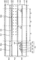
- FIG. 1 is a plan view illustrating a liquid crystal display according to an exemplary embodiment of the present invention.
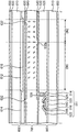
- FIG. 2 is a cross-sectional view for describing a liquid crystal display according to an exemplary embodiment of the present invention.
- 3A to 3I are plan views illustrating structures of first or second electrodes according to embodiments of the present invention.
- FIG. 4 is a graph showing the electrical characteristics of the liquid crystal layer according to an embodiment of the present invention.
- 5A to 5E are graphs comparing the transmittances of the liquid crystal display devices of Examples 1 to 4 and the liquid crystal display devices of Comparative Examples 1 to 3.
- 5F is a graph comparing the transmittances of the liquid crystal display devices of Examples 3 and 9 and the liquid crystal display device of Comparative Example 3.
- FIG. 5F is a graph comparing the transmittances of the liquid crystal display devices of Examples 3 and 9 and the liquid crystal display device of Comparative Example 3.
- 6A to 6D are graphs comparing the response speeds of the liquid crystal display devices of Examples 1 to 4 and the liquid crystal display devices of Comparative Examples 1 to 3.
- FIG. 6E is a graph comparing the response speeds of the liquid crystal display of Example 3 and 9 and the liquid crystal display of Comparative Example 3.
- FIG. 6E is a graph comparing the response speeds of the liquid crystal display of Example 3 and 9 and the liquid crystal display of Comparative Example 3.
- FIG. 7A is a graph illustrating transmittances of the liquid crystal displays of Examples 5 to 8
- FIG. 7B is a graph illustrating response speeds of the liquid crystal displays of Examples 5 to 8.
- 8A to 8C and 9A to 9C are textures of the liquid crystal display of Comparative Examples 1, 3, and 9, respectively.
- 10A and 10B are graphs showing gray levels of the textures of 7A, 7B, 8A, and 8B.
- 11A and 11B are graphs showing transmittances according to voltages applied to the textures of Comparative Examples 1, 3, and 9;
- FIGS. 12A, 2A, and 14A are perspective views illustrating a liquid crystal display according to an exemplary embodiment of the present invention.
- 12B, 13B, and 13B are cross-sectional views for describing a liquid crystal display device according to an exemplary embodiment of the present invention.
- 12C, 13C, and 14C are plan views illustrating a liquid crystal display according to an exemplary embodiment of the present invention.
- 15A and 15B are plan views and cross-sectional views for describing a liquid crystal display according to an exemplary embodiment of the present invention.
- 16A through 16F are plan views illustrating structures of first and second electrodes according to example embodiments.
- 17A and 17B are graphs comparing the transmittances of the liquid crystal display devices of Examples 1 and 2 and the liquid crystal display devices of Comparative Examples 1 and 2.
- FIG. 17A and 17B are graphs comparing the transmittances of the liquid crystal display devices of Examples 1 and 2 and the liquid crystal display devices of Comparative Examples 1 and 2.
- FIG. 18 is a graph comparing response speeds of the liquid crystal display devices of Examples 1 and 2 and the liquid crystal display devices of Comparative Examples 1 and 2.
- FIG. 18 is a graph comparing response speeds of the liquid crystal display devices of Examples 1 and 2 and the liquid crystal display devices of Comparative Examples 1 and 2.
- 19A, 19B, 20A, and 20B are textures of the liquid crystal display of Comparative Example 1 and Example 1.
- FIG. 19A, 19B, 20A, and 20B are textures of the liquid crystal display of Comparative Example 1 and Example 1.
- 21A and 21B are graphs illustrating gray levels of the liquid crystal display of Comparative Example 1 and Example 1.
- FIG. 21A and 21B are graphs illustrating gray levels of the liquid crystal display of Comparative Example 1 and Example 1.
- 22A and 22B are graphs illustrating transmittances according to predetermined intervals of textures of the liquid crystal display of Comparative Examples 1 and 1.
- FIG. 23 is a plan view illustrating a liquid crystal display according to an exemplary embodiment of the present invention.
- FIG. 24 is a cross-sectional view for describing a liquid crystal display according to an exemplary embodiment of the present invention.
- 25A and 25B are graphs comparing the transmittances of the liquid crystal display devices of Examples 12 to 16 and the liquid crystal display devices of Comparative Examples 6 to 10;
- 26A and 26B are graphs comparing the response speeds of the liquid crystal display devices of Examples 12 to 16 and the liquid crystal display devices of Comparative Examples 6 to 10;
- 27A to 27K are textures that change according to a voltage applied to the liquid crystal display of the sixteenth embodiment.
- 29 is a plan view illustrating a liquid crystal display according to an exemplary embodiment of the present invention.
- FIG. 30 is a cross-sectional view for describing a liquid crystal display according to an exemplary embodiment of the present invention.
- 31A and 31B are graphs comparing the transmittances of the liquid crystal display devices of Examples 17 to 22 and the liquid crystal display devices of Comparative Examples 11 to 16.
- FIG. 31A and 31B are graphs comparing the transmittances of the liquid crystal display devices of Examples 17 to 22 and the liquid crystal display devices of Comparative Examples 11 to 16.
- 32A and 32B are graphs comparing the response speeds of the liquid crystal displays of Examples 17 to 22 and the liquid crystal displays of Comparative Examples 11 to 16.
- 33A to 33K are textures that change according to a voltage applied to the liquid crystal display of Example 21.
- FIG. 33A to 33K are textures that change according to a voltage applied to the liquid crystal display of Example 21.
- 34A to 34K are textures that change according to a voltage applied to the liquid crystal display of Comparative Example 15.
- FIGS. 34A to 34K are textures that change according to a voltage applied to the liquid crystal display of Comparative Example 15.
- a film (or layer) is on another film (or layer) or substrate, it may be formed directly on another film (or layer) or substrate or a third film ( Or layers) may be interposed.
- first, second, third, etc. are used to describe various regions, films (or layers), etc. in various embodiments of the present specification, these regions, films should not be limited by these terms. do. These terms are only used to distinguish any given region or film (or layer) from other regions or films (or layers). Therefore, the film quality referred to as the first film quality in one embodiment may be referred to as the second film quality in other embodiments.
- first film quality in one embodiment
- second film quality in other embodiments.
- Each embodiment described and illustrated herein also includes its complementary embodiment. Portions denoted by like reference numerals denote like elements throughout the specification.
- 1 and 2 are a plan view and a cross-sectional view for describing a liquid crystal display according to an exemplary embodiment of the present invention.
- the liquid crystal display includes a first display panel 100, a second display panel 200 spaced apart from and facing the first display panel 100, and the first and second display panels. It may include a liquid crystal layer 300 disposed between (100, 200).
- the liquid crystal display may further include a first polarizer 400 and a second polarizer 450 having a transmission axis perpendicular to the transmission axis of the first polarizer 400.
- the first display panel 100 may include a first substrate 110, a thin film transistor (TFT), and a first electrode 130.
- the first substrate 110 may include a transparent insulating material such as glass.
- the thin film transistor may be disposed on one surface of the first substrate 110.
- the thin film transistor TFT may include a gate electrode 112, a gate insulating layer 114, a semiconductor 116, a source electrode 122, and a drain electrode sequentially stacked. electrode, 124).
- the gate electrode 112 may include a single layer or multiple layers of metals or metal alloys, and the gate insulating layer 114 may include silicon oxide, silicon nitride, or silicon oxynitride.
- the intrinsic semiconductor 116 may include amorphous silicon.
- the source electrode 122 and the drain electrode 124 may be spaced apart from each other on the intrinsic semiconductor 116.
- a channel of the thin film transistor TFT may be formed in the intrinsic semiconductor 116 between the source electrode 122 and the drain electrode 124.
- the source electrode 122 may be electrically connected to a data line DL and may receive a data voltage from the data line DL.
- the drain electrode 124 may be electrically connected to the first electrode 130.
- the thin film transistor TFT may further include ohmic contacts 118 and 120 disposed between the intrinsic semiconductor 116 and the source and drain electrodes 122 and 124.
- the ohmic contacts 118 and 120 may include silicide or n + hydrogenated amorphous silicon doped with a high concentration of n-type impurities.
- a first insulating layer 126 having a contact hole 128 may be formed on the thin film transistor TFT.
- the first insulating layer 126 may include an inorganic insulating material such as silicon oxide, silicon nitride, silicon oxynitride, or an organic insulating material such as resin.
- the contact hole 128 may expose an upper surface of the drain electrode 124.
- the first electrode 130 may be formed on the first insulating layer 126.
- the first electrode 130 may be a pixel electrode.
- the first electrode 130 may be electrically connected to the drain electrode by a contact hole.
- the first electrode 130 may receive a data voltage from the drain electrode.
- the first electrode 130 may include a transparent conductive material such as indium tin oxide (ITO) or indium zinc oxide (IZO).
- the first electrode 130 may include domain dividing means, for example, first slits 132a and 132b.
- the first slits 132a and 132b may be portions in which the first electrode 130 is removed so that the first electrode 130 has a pattern.
- the first slits 132a and 132b generate an electric field between the first and second electrodes 130 and 230.
- the electric field may be formed to be inclined simultaneously with vertical and horizontal components instead of perpendicular to the surface of the first substrate 110.
- the domain dividing means may have a protrusion shape which is formed on the first electrode 130 and protrudes from the first electrode 130 in the direction of the liquid crystal layer 300.
- the first electrode 130 may have various structures.
- the structure of the first slits 132a and 132b of the first electrode 130 will be described in detail below.
- the first display panel 100 may further include a first alignment layer 140 between the first electrode 130 and the liquid crystal layer 300.
- the first alignment layer 140 may pre-tilt the liquid crystal molecules in the liquid crystal layer 300 in one direction.
- the first alignment layer 140 is a group consisting of poly-amic acid, polyimide, lecithin, nylon, polyvinylalcohol (PVA). It may include at least one selected from.
- the first alignment layer 140 may further include a reactive mesogen material.
- the first polarizer 400 may be disposed on the other surface of the first substrate 110.
- the other surface of the first substrate 110 may be a surface corresponding to the one surface.
- the second display panel 200 may include a second substrate 210 and a second electrode 230.
- the second substrate 210 may include a transparent insulating material such as glass.
- the second electrode 230 may be disposed on one surface of the second substrate 210, and one surface of the second substrate 210 may be a surface facing the first display panel 100.
- the second electrode 230 may be a common electrode.
- the second electrode 230 may include a transparent conductive material such as ITO or IZO.
- the second electrode 230 may include domain dividing means, for example, second slits 232a and 232b.
- the second slits 232a and 232b may be portions in which the second electrode 230 is removed to allow the second electrode 230 to have a pattern.
- the second slits 232a and 232b generate an electric field between the first and second electrodes 130 and 230.
- the electric field may be formed to be inclined simultaneously with vertical and horizontal components instead of perpendicular to the surface of the second substrate 210.
- the second electrode 230 may have a protrusion shape protruding from the second electrode 230 toward the liquid crystal layer 300.
- the second electrode 230 may have various structures.
- the structure of the second slits 232a and 232b of the second electrode 230 will be described in detail below.
- the liquid crystal display may be a liquid crystal display in a patterned vertical alignment (PVA) mode. Therefore, although the first electrode 130 having the first slits 132a and 132b and the second electrode 230 having the second slits 232a and 232b face each other, the first slits 132a and 132b do not face each other. And the second slits 232a and 232b do not face each other.
- the first electrode 130 having the first slits 132a and 132b and the second electrode 230 having the second slits 232a and 232b may have substantially the same structure.
- the first and second electrodes 130 and 230 may be disposed so that the slits 132a and 132b and the second slits 232a and 232b do not face each other.
- the first and second electrodes 130 and 230 may have different structures, and the first slits 132a and 132b of the first electrode 130 and the second electrode 230 may be formed.
- the two slits 232a and 232b may not face each other.
- the first slits 132a and 132b and the second slits 232a and 232b may be spaced apart from each other without substantially overlapping each other in a plan view.
- the first slits 132a and 132b and the second slits 232a and 232b may be alternated when viewed in a plan view.
- a voltage is applied by the first slits 132a and 132b and the second slits 232a and 232b of the first and second electrodes 130 and 230.
- An inclined electric field may be formed between the first and second electrodes 130 and 230.
- multi-domains D1 to D4 may be formed in one pixel.
- liquid crystal molecules are arranged in four directions, whereby four domains D1 to D4 may be formed in one pixel.
- it does not limit the number of domains formed in the pixel.
- the second display panel 200 may further include a color filter 212.
- the color filter 212 may be disposed between the second substrate 210 and the second electrode 230.
- a light blocking member 214 may be disposed on one surface of the second substrate 210, and the color filter 212 may be formed in each area defined by the light blocking member 214.
- the color filter 212 may be protected by the second insulating layer 216.
- the color filter 212 is described as being disposed on the second display panel 200, but the color filter 212 may be disposed on the first display panel 100. In the present invention, the position of the color filter 212 is not limited.
- the second display panel 200 may further include a second alignment layer 240 between the second electrode 230 and the liquid crystal layer 300.
- the second alignment layer 240 may initially align the liquid crystal molecules in the liquid crystal layer 300 in one direction.
- the second alignment layer 240 is a group consisting of poly-amic acid, polyimide, lecithin, nylon, polyvinylalcohol (PVA). It may include at least one selected from.
- the second alignment layer 240 may further include a reactive mesogen material.
- the second polarizer 450 may be disposed on the other surface of the second substrate 210.
- the other surface of the second substrate 210 may be a surface corresponding to the one surface.
- the second polarizer 450 may pass a linear polarization component that vibrates in a vertical direction among the light passing through the first polarizer 400.
- the liquid crystal layer 300 may fill between the first and second display panels 100 and 200.
- the liquid crystal layer 300 may include a negative nematic liquid crytal having a negative dielectric anisotropy, a positive nematic liquid crytal having a positive dielectric anisotropy, and a ferroelectric liquid. crystal).
- the liquid crystal layer 300 may include a non-ferroelectric liquid crystal and a ferroelectric liquid crystal. Description of the liquid crystal layer 300 will be described in detail below.
- the liquid crystal display may further include an optical compensation film 430.
- the optical compensation film 430 may be disposed between the second polarizing plate 450 and the second substrate 210.
- the polarization axes of the first polarizing plate 400 and the second polarizing plate 450 are perpendicular to each other so that light leakage does not occur, but when viewed from the side, the first and second polarizing plates Light leakage may occur because the polarization angle of the polarization axes of the fields 400 and 450 is increased.
- an optical compensation film 430 such as a biaxial film or a uniaxial film may be disposed.
- the liquid crystal layer 300 of the liquid crystal display of the PVA mode includes the ferroelectric liquid crystal
- the alignment of the liquid crystal layer in addition to the nematic liquid crystal can be improved and the stability of the alignment can be improved. Therefore, the luminance of the liquid crystal display including the liquid crystal layer 300 may be improved.
- the alignment speed of the liquid crystal molecules in the liquid crystal layer 300 is increased, and the angle of the alignment is also increased, thereby providing optical characteristics. This can be improved.
- the electrode structure described below is representatively described as an example of the first electrode 130, but the second electrode 230 may have one of the following electrode structures. As described above, if the first slits 132a and 132b and the second slits 232a and 232b do not face each other, the structures of the first and second electrodes may be the same or different, and the structure may be variously changed. It is possible.
- 3A to 3I are plan views illustrating structures of the first and second electrodes 130 and 230 according to embodiments of the present invention.
- the first electrode 130 may have a Chevron pattern.
- the first slits 132a and 132b of the first electrode 130 have a V-shape, and have a first line 132a extending in the first direction D1 and a second crossing the first direction D1.
- the second line 132b extending in the direction D2 may be connected.
- the first electrode 130 may have a modified Chevron pattern.
- the structure of the first slits 132a and 132b is similar to that shown in FIG. 3A, but the middle of the first line 132a is cut by the first electrode 130 and the middle of the second line 132b. It may have a structure cut by the first electrode 130.
- the first electrode 130 may have an X-shaped pattern.
- the structures of the first slits 132a and 132b include a first line 132a extending in the first direction D1 and a second line 132b extending in the second direction D2 crossing the first direction D1. ) May be included. Unlike FIG. 3A, the first and second lines 132a and 132b are not connected to each other.
- the first electrode 130 may have a stripe pattern.
- the structure of the first slit 132 may have a form in which lines extending in one direction are repeatedly provided in parallel with each other.
- the first electrode 130 may have a grid pattern.
- the structures of the first slits 132a and 132b include a first line 132a extending in a first direction D1 and a second line extending in a second direction D2 perpendicular to the first direction D1 ( 132b) may be connected to the structure.
- the first electrode 130 may have square patterns, and each of the square patterns may include four triangles divided into diagonals of the square pattern.
- the structures of the first slits 132a, 132b, and 132c may be divided into four rectangular patterns and four triangles within the rectangular patterns. More specifically, the first slits 132a, 132b, and 132c may include a first line 132a extending in the first direction D1 and a second extension D2 different from the first direction D1. And a third line 132c extending in a third direction D3 that intersects the second line 132b and the second direction D2, and the first and second lines 132a and 132b each other. The first and third lines 132a and 132c may be connected to each other.
- the first electrode 130 may have square patterns, and each of the square patterns may include two triangles divided diagonally of the square pattern.
- the structures of the first slits 132a and 132b may divide the rectangular pattern and divide the two triangles in the rectangular patterns. More specifically, the first slit includes a first line 132a extending in the first direction D1 and a second line 132b extending in a second direction D2 different from the first direction D1. can do.
- the first and second lines 132a and 132b may be connected to each other.
- the first electrode 130 may have square patterns and may include a circular first slit 132a in the square pattern.
- the first slit 132a in the square pattern is circular, but the first slit 132a may be polygonal.
- the first slit may further include a structure 132b that divides the square patterns.
- the first electrode 130 may include a plurality of circular first slits 132.
- the first slits 132 may be spaced apart from each other at equal intervals and arranged in rows / columns.
- the first slits 132 are shown in a circular shape, but the first slits 132 may be polygonal.
- liquid crystal layer will be described in detail.
- the liquid crystal layer according to the embodiments of the present invention may include a negative nematic liquid crystal having negative dielectric anisotropy, a positive nematic liquid crystal having positive dielectric anisotropy, and a ferroelectric liquid crystal. ) May be included.
- the liquid crystal layer may include a nematic liquid crystal having negative dielectric anisotropy of about 70 wt% to about 99.9 wt%.
- the liquid crystal layer may further include a mixture of nematic liquid crystals and ferroelectric liquid crystals having dielectric anisotropy in an amount of about 0.1% to about 30% by weight.
- the mixture of the positively anisotropic nematic liquid crystal and the ferroelectric liquid crystal includes a nematic liquid crystal having an amount of dielectric anisotropy of about 1% by weight to 90% by weight, and about 10% by weight to about 99% by weight of the ferroelectric liquid crystal. can do.
- the ferroelectric liquid crystal in the liquid crystal layer may be in the range of about 0.01% to about 29.7% by weight.
- the ferroelectric liquid crystal is about 0.01% by weight or less of the total amount of the liquid crystal layer, the liquid crystal alignment of the liquid crystal layer may be unstable.
- the ferroelectric liquid crystal exceeds about 29.7% by weight of the total amount of the liquid crystal layer, the viscosity of the liquid crystal layer may increase, resulting in a slow response time of the display device including the liquid crystal layer.
- the ferroelectric liquid crystal may be about 10% by weight of the total amount of the liquid crystal layer.
- exemplary materials of the nematic liquid crystal having negative dielectric anisotropy, the nematic liquid crystal having positive dielectric anisotropy and the ferroelectric liquid crystal will be described.
- Exemplary materials described below do not limit the nematic liquid crystals having negative dielectric anisotropy, the nematic liquid crystals having positive dielectric anisotropy, and ferroelectric liquid crystals of the present invention.
- nematic liquid crystals First, the characteristics of nematic liquid crystals will be briefly described, and examples of nematic liquid crystals having negative dielectric anisotropy and nematic liquid crystals having positive dielectric anisotropy will be classified.
- Nematic liquid crystals form liquid crystals in which the elongated molecules of the liquid crystal have irregular positions of each other but their long axes are directed in a constant direction. Since each molecule of the nematic liquid crystal can freely move in the long axis direction, the viscosity is small and easily flows. Since the directions of the nematic molecules are substantially the same in the up and down directions, the polarization is canceled and generally does not exhibit ferroelectricity. In the direction perpendicular to the axial direction of the molecules of the liquid crystal, physical properties are very different. Therefore, nematic liquid crystal is a material having optical anisotropy.
- nematic liquid crystal with negative dielectric anisotropy If the difference between the dielectric constant parallel to the axial direction and the dielectric constant perpendicular to the axial direction ( ⁇ ) is less than 0, it is called a nematic liquid crystal with negative dielectric anisotropy, and if greater than 0, it is called a nematic liquid crystal with positive dielectric anisotropy. .
- the nematic liquid crystal having negative dielectric anisotropy may include nematic liquid crystal molecules having negative dielectric anisotropy.
- the nematic liquid crystal molecules having negative dielectric anisotropy may be a single type.
- the nematic liquid crystal molecules having negative dielectric anisotropy may be of different kinds from each other.
- the nematic liquid crystal molecules having negative dielectric anisotropy may include liquid crystal molecules having negative dielectric anisotropy having a first dielectric constant and liquid crystal molecules having negative dielectric anisotropy having a second dielectric constant. In this case, the second dielectric constant may be different from the first dielectric constant.
- the nematic liquid crystal having negative dielectric anisotropy may include nematic liquid crystal molecules having negative dielectric anisotropy and first base liquid crystal molecules.
- Each of the first base liquid crystal molecules may include at least one selected from the group consisting of liquid crystal molecules having negative dielectric anisotropy, liquid crystal molecules having positive dielectric anisotropy and neutral liquid crystal molecules.
- the nematic liquid crystal having negative dielectric anisotropy may include nematic liquid crystal molecules having one kind of negative dielectric anisotropy and first base molecules.
- the nematic liquid crystal having negative dielectric anisotropy may include liquid crystal molecules having various kinds of negative dielectric anisotropy and first base liquid crystal molecules.
- nematic liquid crystals having negative dielectric anisotropy will be described with examples.
- the following materials may be used alone or in combination.
- the negative liquid crystal having negative dielectric anisotropy may include a halogen group, a cyanide group, or an isocyanate group nematic liquid crystal.
- the nematic liquid crystal having negative dielectric anisotropy may be used alone or in combination with a halogen group, a cyanide group, or an isocyanate group nematic liquid crystal.
- the nematic liquid crystal having negative dielectric anisotropy may further include first base liquid crystal molecules.
- the nematic liquid crystal having a halogen-based negative dielectric anisotropy may include a fluorine group, a chlorine group, or a bromine group material, and may have a single or polycyclic structure.
- Nematic liquid crystals having a negative dielectric anisotropy of a halogen-based bicyclic structure may be represented by the following Chemical Formulas 1 and 2.
- Nematic liquid crystals having a negative dielectric anisotropy of a halogen-based tricyclic structure may be represented by Chemical Formulas 3 to 6.
- Nematic liquid crystals having a negative dielectric anisotropy of a halogen-based tetracyclic structure may be represented by Chemical Formulas 7 to 9.
- Y represents hydrogen or halogen
- R 1 represents alkyl having 1 to 15 carbon atoms, or alkenyl
- R 2 represents 1 to 15 carbons Alkyl, alkenyl, or alkoxy having atoms (in R 1 , and R 2 , hydrogen may be replaced by CN, CF 3 , or halogen atoms)
- the nematic liquid crystal having halogen negative dielectric anisotropy has a lateral fluorinated indane derivative and may be represented by the following Chemical Formula 10.
- n 0 or 1.
- the nematic liquid crystal having cyanide negative dielectric anisotropy may be represented by the following Chemical Formulas 11 to 13.
- the negative liquid crystal having dielectric anisotropy may be a single substance or a mixture. According to an embodiment, the nematic liquid crystal mixture having negative dielectric anisotropy,
- Liquid Crystal Component A consisting of at least one compound having a dielectric anisotropy of less than -1.5:
- liquid crystal component B consisting of at least one compound having a dielectric anisotropy of -1.5 to +1.5:
- the liquid crystal component A may include one or more compounds of Formulas 14 to 17.
- the liquid crystal component B may include one or more compounds of Formulas 18 to 20.
- the liquid crystal component B may be the first base liquid crystal molecules described above.
- R 4 and R 5 are each independently alkyl, alkoxy, alkoxy alkyl, alkenyl or alkenyloxy having 1 to 15 carbon atoms. oxy), where hydrogen may be substituted by CN, CF 3 , or halogen atoms, and the —CH 2 — group is —CH ⁇ CH—, —O—, —CO—, —COO -, -OOC-, -O-OC-O- or -S- may be substituted), Y 1 represents hydrogen or halogen.
- Chiral component C is available in a number of chiral dopants, such as the following examples.
- the choice of dopant is not important by itself.
- the nematic liquid crystal having positive dielectric anisotropy may include nematic liquid crystal molecules having positive dielectric anisotropy.
- the nematic liquid crystal molecules having the positive dielectric anisotropy may be a single type.
- the nematic liquid crystal molecules having the positive dielectric anisotropy may be of different kinds from each other.
- the nematic liquid crystal molecules having positive dielectric anisotropy may include liquid crystal molecules having positive dielectric anisotropy having a first dielectric constant and liquid crystal molecules having positive dielectric anisotropy having a second dielectric constant. In this case, the second dielectric constant may be different from the first dielectric constant.
- the nematic liquid crystal having positive dielectric anisotropy may include nematic liquid crystal molecules having positive dielectric anisotropy and second base liquid crystal molecules.
- Each of the second base liquid crystal molecules may include at least one selected from the group consisting of liquid crystal molecules having negative dielectric anisotropy, liquid crystal molecules having positive dielectric anisotropy, and neutral liquid crystal molecules.
- the nematic liquid crystal having a positive dielectric anisotropy may include nematic liquid crystal molecules having a kind of dielectric anisotropy and second basis molecules.
- the nematic liquid crystal having positive dielectric anisotropy may include liquid crystal molecules having various kinds of dielectric anisotropy and second base liquid crystal molecules.
- nematic liquid crystals having positive dielectric anisotropy will be described by listing examples.
- the following materials may be used alone or in combination.
- the nematic liquid crystal having a positive dielectric anisotropy may include a nematic liquid crystal having a positive dielectric anisotropy of a cyanide group, an isocyanate group, and a halogen group.
- the nematic liquid crystal having the positive dielectric anisotropy may be used singly or in combination with the cyanide group, the isocyanate group, and the halogen-based nematic liquid crystal having the positive dielectric anisotropy.
- the nematic liquid crystal having the positive dielectric anisotropy may further include second base liquid crystal molecules.
- the nematic liquid crystal having positive dielectric anisotropy may have a bicyclic structure or a tricyclic structure.
- the cyanated nematic liquid crystal of the bicyclic structure may be represented by Chemical Formula 21.
- R 6 in formula 21 is alkenyl having 1 to 15 carbon atoms (wherein hydrogen may be replaced by CN, CF 3 , or halogen, and —CH 2 — group is —CH ⁇ May be optionally substituted by CH—, —O—, —CO—, —COO—, —OOC—, —O—OC—O—, or —S—. Specific examples of Formula 21 are shown below.
- R 7 is H, CH 3 , C 2 H 5 or nC 3 H 7 .
- the nematic liquid crystal having positive dielectric anisotropy of the tricyclic structure may be represented by Chemical Formula 22.
- R 3 is as R 3 is unsubstituted or CN, CF 3, or halogen-alkyl (alkyl) having at least one carbon atom less than the 15-substituted one by (halogen) groups as defined in Formula 11 to 13, wherein One or more CH 2 groups in these alkyls may be replaced by —O—, —S—, —C ⁇ C—, —CH ⁇ CH—, —OC—O— or —O—CO—, L 1 and L 2 each independently is hydrogen or halogen (halogen) with each other.
- Nematic liquid crystals having an isocyanate-based dielectric anisotropy can be represented by the following formula (23).
- R 8 is C n H 2n + 1 O, C n H 2n + 1 , or C n H2 n-1 , wherein n is 1 to 15 and A is or , B is -CH 2 -CH 2 -or -C ⁇ C-, X 1 is hydrogen or halogen, m is 1, 2, 3, or 4. Specific examples of Formula 23 are shown next.
- Nematic liquid crystals having a halogen-based positive dielectric anisotropy may include a fluorine-based or chlorine-based material and may have a single or polycyclic structure. Nematic liquid crystals having fluorine-based dielectric anisotropy may be represented by Chemical Formulas 24 to 27.
- the nematic liquid crystal having positive dielectric anisotropy of the halogen series bicyclic structure may be represented by the following Chemical Formula 28.
- N in the formulas is 1 to 15.
- the nematic liquid crystal having positive dielectric anisotropy of the halogen-based tricyclic structure may be represented by Chemical Formulas 29 to 33.
- R 12 is alkyl or alkenyl having 1 to 15 carbon atoms (wherein alkyl or alkenyl is unsubstituted or at least monosubstituted by CN, CF 3 , or halogen) And one or more -CH 2 -groups may be substituted by -O-), X 3 is -F, -Cl, -OCF 3 , -OCHF 2 , -OCH 2 F or -CF 3 .
- Specific examples of the formula (29) are as follows.
- R 12 is as defined above.
- the nematic liquid crystal having positive dielectric anisotropy of the halogen-based tetracyclic structure may be represented by Chemical Formulas 34 to 36.
- a nematic liquid crystal having a positive dielectric anisotropy containing a trisubstituted fluorine or cyanide group may be represented by the formula (37).
- At least one of two R 14 and R 15 is an alkenyl group having up to 15 carbon atoms unsubstituted or at least monosubstituted by CN, CF 3 or halogen, and the other One can be an alkyl group having up to 15 carbon atoms unsubstituted or at least monosubstituted by halogen, CN, CF 3 or halogen, wherein one or more CH 2 groups of these groups are -O-, -S May be replaced by-, -C ⁇ C-, -OCO-, or -O-CO-. Specific examples of Formula 37 are shown next.
- n and m are 1 to 10, preferably 1 to 5
- o and p are each independently the same or different and are 0 to 10, preferably 0 to 5, provided that the sum of o + p is preferably Is 7 or less.
- the nematic liquid crystals having said positive dielectric anisotropy can be a single substance or a mixture.
- Nematic liquid crystal mixture having a positive dielectric anisotropy according to one embodiment,
- liquid crystal component A consisting of one or more compounds having a dielectric anisotropy greater than +1.5
- liquid crystal component consisting of one or more compounds having a dielectric anisotropy of -1.5 to +1.5
- Liquid crystal component A may include one or more compounds of Formula 37.
- Liquid crystal component B may include one or more compounds represented by Formula 38 below.
- the liquid crystal component B may be the second base liquid crystal molecules described above.
- Component C is cholesteryl nonanoate (CN), S-811, S-1011, S-2011 (Merck KGaA, Darmstadt, Germany) with multiple chiral dopants and CB15 (Pool, UK). Many chiral dopants are available, such as BDH). The choice of dopant is not important by itself.
- R 16 and R 17 are each independently the same or different and each is an alkyl group having up to 15 carbon atoms which are unsubstituted or at least monosubstituted by CN, CF 3, or halogen, Wherein one or more CH 2 in these alkyl groups may be replaced by —O—, —S—, —C ⁇ C—, —CH ⁇ CH—, —OC—O— or —OCO—, wherein 1,4- The phenylene (1,4-phenylene) ring may be mono- or polysubstituted by fluorine independently of each other.
- ferroelectric liquid crystals have spontaneous polarization even when an electric field is not applied, it is a kind of dielectric that is an electrically insulator, but unlike general dielectrics, dielectric polarization is not proportional to electric field, and the relationship between polarization and electric field It has the characteristic which shows the ideal with electric history. Ferroelectric liquid crystals have not only spontaneous polarization, but also physical properties in which spontaneous polarization is reversed by an electric field.
- the ferroelectric liquid crystal may include ferroelectric liquid crystal molecules.
- the ferroelectric liquid crystal molecules may be a single type.
- the ferroelectric liquid crystal molecules may be of different kinds from each other.
- the ferroelectric liquid crystal molecules may include a first ferroelectric liquid crystal molecule and a second ferroelectric liquid crystal molecule. In this case, the second ferroelectric liquid crystal molecules may be different from the first ferroelectric liquid crystal molecules.
- the ferroelectric liquid crystal may include ferroelectric liquid crystal molecules and third base liquid crystal molecules.
- Each of the third base liquid crystal molecules may include at least one selected from the group consisting of liquid crystal molecules having negative dielectric anisotropy, liquid crystal molecules having positive dielectric anisotropy, and neutral liquid crystal molecules.
- the ferroelectric liquid crystal may include one type of ferroelectric liquid crystal molecules and third base molecules.
- the ferroelectric liquid crystal may include ferroelectric liquid crystal molecules different from each other and third base molecules.
- ferroelectric liquid crystal will be described by listing examples.
- the following materials may be used alone or in combination.
- the ferroelectric liquid crystal may be chiral.
- the ferroelectric liquid crystal may be a fluorine chiral end ferroelectric liquid crystal, a chiral allyl ester ferroelectric liquid crystal, a center core polyring chiral ferroelectric liquid crystal, or a smear chiral ( smetic chiral) ferroelectric liquid crystal and the like.
- the ferroelectric liquid crystal may be a banana shape ferroelectric liquid crystal.
- the ferroelectric liquid crystals include fluorine chiral end ferroelectric liquid crystals, chiral allyl ester ferroelectric liquid crystals, center core polyring chiral ferroelectric liquid crystals, and smetic chiral ferroelectric liquid crystals. Liquid crystals and banana shape ferroelectric liquid crystals may be used alone or in combination.
- the ferroelectric liquid crystal may further include third base liquid crystal molecules.
- the fluorine-based chiral terminal ferroelectric liquid crystal may be represented by the following Chemical Formula 39.
- X 4 , X 5 , X 6 and X 7 are each independently CF 3 , CF 2 H , CFH 2 , halogen, alkyl or alkoxy, and C and D are independently Phenyl, mono-fluorophenyl, di-fluorophenyl, or cyclo-hexyl, E is independently a single bond, COO, OOC, and C ⁇ C Is selected from at least one of E is a single bond, q is 0 or 1, and R 18 is a terminal group of the formula (40).
- Z is O, (CH 2 ) 1 O, or (CH 2 ) 2 O
- J and M are independently selected from hydrogen, alkyl of 1 to 15 carbon atoms
- W is a carbon atom 1 to 15 straight or branched alkyl chains, each of J, M and W different
- R 19 represents alkenyl, alkenyloxy, alkynyl containing from 1 to 15 carbon atoms ), Or alkynoxy.
- the chiral aryl ester liquid crystal may be represented by Chemical Formula 41.
- Q represents a alkyl group substituted with alkyl or halogen, and * represents an optically active carbon.
- Specific examples of formula 41 include 4'-n- (octyloxyphenyl4 '-(1,1,1-trifluoro-2-octyloxycarbonyl) biphenyl-4-carboxylate (4) '-n- (octyleoxyphenyl 4'-(1,1,1-trigluoro-2-octyloxycarbonyl) biphenyl-4-carboxylate).
- the central core polyring chiral ferroelectric liquid crystal may be represented by Chemical Formulas 42 to 44.
- Formula 42 is formulated as S-4- (trans-4-heptylcyclohexyl) -3'-chloro-4 "-(1-methylheptyloxy) terphenyl (S-4- (trans-4-heptylcyclohexyl) -3'- chloro-4 "-(1-methylheptyloxy) terphenyl).
- Formula 43 represents R-4-octyl-3 "-chloro-4 '' '-(1-methylhexyloxy) quaterphenyl (R-4-octhyl-3" -chloro-4' ''-(1-methylhexyloxy ) quarterphenyl).
- Formula 44 is formulated as S-4-nonyl-3'-fluoro-4 '' '-(2-chloropropyloxy) quaterphenyl (S-4-nonyl-3'-fluoro-4' ''-(2-chloropropyloxy ) quarterphenyl).
- Formula 45 is butyl S-2- (4-octyl-2'-fluoro-3 "-trifluoromethyl-4 '' '-quaterphenyloxy) -propionate (S-2- (4-octyl- 2'-fluoro-3 "-trifluoromethyl-4 '' '-quarterphenyloxy) -propionate).
- the ferroelectric smetic liquid crystal may be represented by at least one of Chemical Formulas 46 and 47.
- R 20 and R 21 each represent a linear alkyl group having 1 to 9 carbon atoms
- R 22 and R 23 each represent the same or different linear alkyl group having 1 to 18 carbon atoms
- hydrogen may be substituted by CN, CF 3 , or halogen atom
- —CH 2 — group is —CH ⁇ CH—, —O—, —CO—, —COO— , -OOC-, -O-OC-O- or -S-
- X represents hydrogen or halogen.
- the chiral smear ferroelectric liquid crystal may be represented by Chemical Formula 48.
- R 24 is chiral or achiral alkyl or alkenyl having 1 to 20 carbon atoms
- R 25 is chiral or achiral having 1 to 20 carbon atoms alkoxy
- Alkenyloxy, alkylcarbonyloxy (alkyl-COO-) or alkenylcarbonyloxy (alkenyl-COO-) (in R 24 and R 25 , hydrogen is CN, CF 3 , or a halogen atom
- L 10 to L 14 is hydrogen, halogen, cyano
- the banana-type ferroelectric liquid crystal may be represented by the following Chemical Formula 49.
- a 1 is or And B1 is or R 26 and R 27 are each independently hydrogen or halogen, and R 28 and R 29 are independently alkyl or alkoxy having 8 to 16 carbon atoms. Specific examples of Formula 49 are shown below.
- the ferroelectric liquid crystal may be a single material of the ferroelectric liquid crystal or a mixture including the ferroelectric liquid crystal.
- X 10 is hydrogen (H)
- R 30 is hydrogen or alkyl of 1 to 15 carbon atoms
- At least one hydrogen of the alkyl, alkenyl group may be replaced by fluorin or CH 3
- R 32 , R 33 , R 34 , and R 35 are each CH 3 .
- the induced dipole is parallel to the electric field, and the nematic liquid crystal having negative dielectric anisotropy is arranged in a direction perpendicular to the electric field.
- the ferroelectric liquid crystal of the liquid crystal layer has a large array characteristic between molecules and an array characteristic according to an electric field, the alignment of the liquid crystal layer can be uniformly stabilized.
- the liquid crystal layer may further include a reactive mesogen material.
- the liquid crystal layer comprises about 0.01 wt% to about 3 wt% reactive mesogen material, about 70 wt% to about 99.9 wt% of negative dielectric anisotropy, and about 0.1 wt% of the liquid crystal layer.
- the reactive mesogenic material means a polymerizable mesogenic compound.
- a "mesogenic compound” or “mesogenic material” can include a substance or compound comprising one or more rod-shaped, plate- or disc-shaped mesogenic groups, ie groups having the ability to induce liquid crystalline phase behavior.
- the reactive mesogen material may be a material which is polymerized by light such as ultraviolet rays and is oriented according to the alignment state of adjacent materials.
- Examples of the reactive mesogen material include compounds represented by the following formula:
- P1 and P2 are at least one of acrylate, methacrylate, vinyl, vinyloxy and epoxy groups, and A1 and A2 are 1,4-phenylene (phenylen) and naphthalene (naphthalene) -2,6-diyl group is at least one, Z1 is one of COO-, OCO- and a single bond, n may be one of 0, 1 and 2.
- P1 and P2 may include at least one of acrylate, methacrylate, vinyl, vinyloxy, and epoxy groups.
- the alignment of the liquid crystal layer together with the nematic liquid crystal may be uniform and the stability of the alignment may be improved.
- the liquid crystal layer includes a reactive mesogen material, the alignment speed of the liquid crystal layer may be increased, and the angle at which the liquid crystal layer is aligned may be increased, thereby improving optical characteristics.
- the liquid crystal layer according to the embodiments of the present invention may include a non-ferroelectric liquid crystal and a ferroelectric liquid crystal.
- the non-ferroelectric liquid crystal may include a nematic liquid crystal having negative anisotropy.
- the ferroelectric liquid crystal may occupy about 0.1 wt% to about 30 wt% of the total amount of the liquid crystal layer.
- the ferroelectric liquid crystal is about 0.1% by weight or less of the total amount of the liquid crystal layer, the liquid crystal alignment of the liquid crystal layer may be unstable.
- the ferroelectric liquid crystal exceeds about 30% by weight of the total amount of the liquid crystal layer, the viscosity of the liquid crystal layer may increase, thereby slowing the response speed of the display device including the liquid crystal layer.
- the ferroelectric liquid crystal may be about 10% by weight of the total amount of the liquid crystal layer.
- the liquid crystal layer may further include a reactive mesogen material.
- the liquid crystal layer comprises about 0.1 wt% to about 30 wt% ferroelectric liquid crystal, about 0.01 wt% to about 3 wt% reactive mesogen material, and nematic liquid crystal having extra negative dielectric anisotropy. It may include.
- the components, structures, and examples of the negatively anisotropic nematic liquid crystal, the ferroelectric liquid crystal, and the reactive mesogen material described in this embodiment are substantially the same as those described above, and a detailed description thereof will be omitted.
- the non-ferroelectric liquid crystal may include a nematic liquid crystal having positive anisotropy and a nematic liquid crystal having negative anisotropy.
- the liquid crystal layer may include a nematic liquid crystal having negative dielectric anisotropy of about 70% by weight to about 99.9% by weight.
- the liquid crystal layer may further include a mixture of nematic liquid crystals and ferroelectric liquid crystals having dielectric anisotropy in an amount of about 0.1% to about 30% by weight.
- the mixture of the positively anisotropic nematic liquid crystal and the ferroelectric liquid crystal includes a nematic liquid crystal having an amount of dielectric anisotropy of about 1% by weight to 90% by weight, and about 10% by weight to about 99% by weight of the ferroelectric liquid crystal. can do.
- the liquid crystal layer may further include a reactive mesogen material.
- the liquid crystal layer comprises a mixture of nematic liquid crystal and ferroelectric liquid crystal having dielectric anisotropy in an amount of about 0.1% by weight to about 30% by weight, about 0.01% by weight to 3% by weight of reactive mesogen material, Nematic liquid crystals with extra negative anisotropy.
- the components, structures, and examples of the negatively anisotropic nematic liquid crystal, the positively anisotropic nematic liquid crystal, the ferroelectric liquid crystal, and the reactive mesogen material described in the present embodiment are substantially the same as those described above. The description will be omitted.
- the alignment of the liquid crystal layer together with the non-ferroelectric liquid crystal may be uniform and the stability of the alignment may be improved.
- the liquid crystal layer includes a reactive mesogen material, the alignment speed of the liquid crystal layer may be increased, and the angle at which the liquid crystal layer is aligned may be increased, thereby improving optical characteristics.
- the liquid crystal layer may be prepared by mixing a nematic liquid crystal having negative anisotropy, a nematic liquid crystal having positive dielectric anisotropy, and a ferroelectric liquid crystal.
- the liquid crystal layer is a mixture of a nematic liquid crystal having a negative dielectric anisotropy of about 70% by weight to about 99.9% by weight, and a nematic liquid crystal and a ferroelectric liquid crystal having a positive dielectric anisotropy of about 0.1% by weight to about 30% by weight. It can be prepared by mixing.
- the mixture of the nematic liquid crystal having a positive anisotropy and the ferroelectric liquid crystal is a nematic liquid crystal having a dielectric anisotropy in an amount of about 1% by weight to 90% by weight, and about 10% by weight to about 99% by weight of the ferroelectric It can be prepared by mixing the liquid crystal.
- the liquid crystal layer may further include a reactive mesogen material.
- the liquid crystal layer comprises a mixture of about 0.01% to 3% by weight reactive mesogen material, a mixture of nematic liquid crystals and ferroelectric liquid crystals having dielectric anisotropy in an amount of about 0.1% to about 30% by weight, It can be prepared by mixing a nematic liquid crystal having a negative dielectric anisotropy of.
- the liquid crystal layer may be prepared by mixing a nematic liquid crystal having a negative anisotropy and a ferroelectric liquid crystal. More specifically, it may be prepared by mixing a nematic liquid crystal having a negative dielectric anisotropy of about 70% by weight to about 99.9% by weight with a ferroelectric liquid crystal of about 0.1% by weight to about 30% by weight.
- the liquid crystal layer may further include a reactive mesogen material.
- the liquid crystal layer comprises about 0.01 wt% to about 3 wt% reactive mesogen material, the 0.1 wt% to about 30 wt% ferroelectric liquid crystal, and a nematic liquid crystal having extra negative dielectric anisotropy. It can be prepared by mixing.
- the process temperature may be a temperature at which the largest amount of material in the liquid crystal layer exhibits isotropic characteristics.
- the mixing process temperature may be performed in a temperature range of about 90 °C to about 100 °C.
- the temperature range may be a temperature range when the nematic liquid crystal having negative dielectric anisotropy exhibits isotropic characteristics.
- the mixing of the liquid crystal layer is performed within a temperature range of about 90 ° C. to about 100 ° C., but the present invention does not limit the mixing temperature of the liquid crystal layer.
- FIG. 4 is a graph showing the electrical characteristics of the liquid crystal layer according to an embodiment of the present invention.
- the x-axis of FIG. 1 represents time, the unit is seconds, the y-axis represents the applied voltage, and the unit is volts [V].
- the nematic liquid crystal and the ferroelectric liquid crystal are not in the form of a compound but in the form of a mixture, so that the nematic liquid crystal exhibits its own characteristics and the ferroelectric liquid crystal can express its own characteristics.
- the nematic liquid crystal and the ferroelectric liquid crystal may enhance and / or interfere with each other.
- a liquid crystal display including a liquid crystal layer to fill was prepared.
- the liquid crystal display is manufactured in a patterned vertical alignment (PVA) mode.
- the thickness of the liquid crystal layer of the said liquid crystal display device was produced at 3.8 micrometers.
- the liquid crystal display devices of Examples 2 to 4 were manufactured in the same manner as in Example 1 except for the thickness of the liquid crystal layer.
- the thicknesses of the liquid crystal layers of Examples 2 to 4 refer to Table 1 below.
- a first display panel comprising a first electrode having a first substrate and a first electrode having a first slit of a Sevron pattern, a second display panel comprising a second electrode having a second substrate and a second slit of a Sevron pattern, and the second display panel;
- a liquid crystal display device including a liquid crystal layer filling the first and second display panels is manufactured.
- the liquid crystal display device was manufactured in PVA mode.
- the thickness of the liquid crystal layer of the said liquid crystal display device was produced in 4.3 micrometers.
- the liquid crystal display devices of Examples 6 to 8 were manufactured in the same manner except for the mixing ratio between Example 5, MLC 6608 and KFLC 3 in the liquid crystal layer. See Table 1 below for a mixing ratio between MLC 6608 and KFLC 3 in the liquid crystal layer.
- a first display panel comprising a first electrode having a first substrate and a first electrode having a first slit of a Sevron pattern, a second display panel comprising a second electrode having a second substrate and a second slit of a Sevron pattern, and the second display panel;
- a liquid crystal display device including a liquid crystal layer filling the first and second display panels is manufactured.
- the liquid crystal display device was manufactured in PVA mode.
- the thickness of the liquid crystal layer of the said liquid crystal display device was produced in 4.3 micrometers.
- a first display panel comprising a first electrode having a first substrate and a first electrode having a first slit of a Sevron pattern, a second display panel comprising a second electrode having a second substrate and a second slit of a Sevron pattern, and the second display panel;
- a liquid crystal display device including a liquid crystal layer filling the first and second display panels is manufactured.
- the liquid crystal display device was manufactured in PVA mode.
- the liquid crystal display devices of Comparative Examples 2 and 3 were manufactured in the same manner as in Comparative Example 1 except for the thickness of the liquid crystal layer.
- the thicknesses of the liquid crystal layers of Comparative Examples 2 and 3 refer to Table 1 below.
- Example 1 Liquid crystal layer Liquid crystal layer thickness [ ⁇ m] MLC 6608 [wt%] (negative nematic liquid crystal) KFLC 3 [wt%] (ferroelectric liquid crystal) ZKC-5085 [wt%] (positive nematic liquid crystal)
- Example 1 90 10 0 3.8
- Example 2 90 10 0 4.0
- Example 3 90 10 0 4.3
- Example 4 90 10 0 4.5 Comparative Example 1 100 0 0 4.3 Comparative Example 2 100 0 0 4.5 Comparative Example 3 100 0 0 4.8
- Example 5 99 One 0 4.3 Example 6 95 5 0 4.3 Example 7 80 20 0 4.3 Example 8 70 30 0 4.3
- Example 9 90 5 5 5 4.3
- 5A to 5E are graphs comparing the transmittances of the liquid crystal display devices of Examples 1 to 4 and the liquid crystal display devices of Comparative Examples 1 to 3.
- 5F is a graph comparing the transmittances of the liquid crystal display of Comparative Example 1, Example 3, and Example 9. FIG.
- 5A to 5C are graphs showing transmittance according to applied voltage.
- the x-axis is an applied voltage and a unit is [V]
- the y-axis represents transmittance.
- FIG. 5A the liquid crystal display of Examples 1 to 4 exhibits excellent overall transmittance as compared to Comparative Examples 1 to 3.
- FIG. 5B selectively shows the transmittance of Example 4 and Comparative Example 2 in FIG. 5A. Referring to FIG. 5B, it was observed that the transmittance of Example 4 was superior to that of Comparative Example 2 at the same liquid crystal layer thickness of 4.5 ⁇ m.
- FIG. 5C optionally shows the transmittance of Example 4 and Comparative Example 3 in FIG. 5A. Referring to FIG. 5C, when Example 4, which has the highest transmittance among Examples 1 to 4, and Comparative Example 3, which has the highest transmittance among Comparative Examples 1 to 3, are compared, it was observed that the transmittance of Example 4 was excellent.
- FIG. 5D and 5E are graphs illustrating transmittance according to the thickness of a liquid crystal layer after applying a voltage of 7 V to the liquid crystal display devices of Examples 1 to 4 and the liquid crystal display devices of Comparative Examples 1 to 3. More specifically, FIG. 5D is a graph showing the transmittance according to the thickness of the liquid crystal layer, and FIG. 5E is a transmittance according to the product ( ⁇ n ⁇ d) of the thickness (d) of the liquid crystal layer and the refractive index ( ⁇ n) of the liquid crystal layer. It is a graph showing. 5D and 5E, the length of the x axis is [ ⁇ m], and the y axis shows transmittance.
- the transmittance of the liquid crystal display devices of Examples 1 to 4 is about 17% to about 30% superior to that of the liquid crystal display devices of Comparative Examples 1 to 3.
- the transmittance of the liquid crystal displays of Examples 1 to 4 is about 9% to about 17% superior to the transmittance of the liquid crystal displays of Comparative Examples 1 to 3. It can be seen that.
- the transmittance of the liquid crystal display of Example 3 is superior to that of the liquid crystal display of Comparative Example 1.
- the transmittance of the liquid crystal display of Example 9 containing 5% by weight of nematic liquid crystal ZKC-5085 having positive dielectric anisotropy is superior to that of the liquid crystal display of Comparative Example 1.
- the liquid crystal display of Examples 1 to 4 and 9 since the ferroelectric liquid crystals in the liquid crystal layers of Examples 1 to 4 and 9 induce the liquid crystal molecules to be uniformly and stably aligned, the liquid crystal display of Examples 1 to 4 and 9 The transmittance is superior to the transmittance of the liquid crystal display of Comparative Examples 1 to 3.
- 6A to 6D are graphs comparing the response speeds of the liquid crystal display devices of Examples 1 to 4 and the liquid crystal display devices of Comparative Examples 1 to 3.
- 6F is a graph comparing response speeds of liquid crystal display devices of Comparative Examples 1, 3, and 9;
- 6A and 6B are graphs illustrating a response speed according to an applied voltage. 6A and 6B, the x-axis is the applied voltage, the unit is [V], and the y-axis represents the response speed.
- the response speeds of the liquid crystal display devices of Examples 1 to 4 are not much slower than those of the liquid crystal display devices of Comparative Examples 1 to 3. Since the liquid crystal layers of Examples 1 to 4 contain ferroelectric liquid crystals, the viscosity of the liquid crystal layers is increased, which is slightly slower than the response speeds of the liquid crystal display devices of Comparative Examples 1 to 3, but seems to be similar.
- FIG. 6B is selectively shown to confirm the response speed according to the voltage of Example 3 showing the maximum transmittance in Examples 1 to 4 and Comparative Example 3 showing the maximum transmittance in Comparative Examples 1 to 3.
- FIG. 6B when comparing the response speeds of Example 3 and Comparative Example 3 having excellent transmittance, it can be seen that the response speed of Example 3 is faster than that of Comparative Example 3.
- FIG. 6B when comparing the response speeds of Example 3 and Comparative Example 3 having excellent transmittance, it can be seen that the response speed of Example 3 is faster than that of Comparative Example 3.
- FIG. 6C and 6D are graphs illustrating a response speed according to a thickness of a liquid crystal layer after applying a voltage of 7 V to the liquid crystal display devices of Examples 1 to 4 and the liquid crystal display devices of Comparative Examples 1 to 3. More specifically, FIG. 6C is a graph showing a response speed according to the thickness of the liquid crystal layer, and FIG. 6D is a response according to the product ( ⁇ n ⁇ d) of the thickness d of the liquid crystal layer and the refractive index ⁇ n of the liquid crystal layer. Graph showing speed. 6C and 6D, the x-axis is the length unit is [ ⁇ m], the y-axis is the response speed is the unit is [ms].
- the response speed of Example 1 having a liquid crystal layer thickness of about 3.8 ⁇ m is about 18 ms, and the liquid crystal layer thickness of at least 4.3 ⁇ m is required to give a response speed of about 18 ms in the comparative examples.
- the response speeds of the liquid crystal display devices of Examples 1 to 4 are about 22% to about 24 times the response speeds of the liquid crystal display devices of Comparative Examples 1 to 3. You can see it's about% faster.
- the response speed of the liquid crystal display of Example 3 was faster than that of the liquid crystal display of Comparative Example 1.
- the response speed of the liquid crystal display of Example 9 in which 5 wt% of the nematic liquid crystal ZKC-5085 having positive dielectric anisotropy is added is also faster than that of the liquid crystal display of Comparative Example 1.
- the liquid crystal display devices of Examples 1 to 4 and 9 have relatively high viscosity. In spite of including the liquid crystal, a response speed faster than that of Comparative Examples 1 to 3 can be achieved by including a liquid crystal layer having an appropriate thickness and refractive index. Therefore, the liquid crystal display of Examples 1 to 4 and 9 not only has a fast response speed but also a stable and uniform alignment of the liquid crystal molecules with the ferroelectric liquid crystal.
- FIG. 7A is a graph illustrating transmittances of the liquid crystal displays of Examples 5 to 8
- FIG. 7B is a graph illustrating response speeds of the liquid crystal displays of Examples 5 to 8.
- the transmittance is improved.
- the response speed is about 2 times slower. Therefore, in the present embodiments, it is preferable that the ferroelectric liquid crystal in the liquid crystal layer does not exceed 30% by weight of the total amount of the composition.
- 8A to 8C and 9A to 9C are textures of the liquid crystal display of Comparative Examples 1, 3, and 9, respectively.
- Comparative Examples 1, 3, and 9 are substantially the same liquid crystal display devices except for the composition ratio of the liquid crystal layer.
- Table 2 shows their composition ratios again.
- the textures of FIGS. 8A-8C are white images under a cross polarizer.
- the white images show a case where the angle between the cross polarizer and the liquid crystal molecules of the liquid crystal layer is 45 °, and the light is passed through the liquid crystal layer and is illuminated. This can be confirmed by Equation 1 below.
- Equation 1 T is the transmittance, ⁇ is the angle between the polarizing plate and the liquid crystal molecules, ⁇ n is the birefringence value, d is the thickness of the liquid crystal layer, ⁇ is the wavelength of the light to be irradiated.
- ⁇ is 45 °, the value of sin 2 has the highest value and the highest transmittance.
- FIG. 8A to 8C are textures of Comparative Example 1, Example 3, and Example 9, respectively.
- FIG. 8A a defect that looks black at the edge portions of the slit or the boundary of the slit is shown.
- FIG. 8B it can be seen that the defects disappeared much compared to FIG. 8A at the edge portion of the slit.
- FIG. 8C it can be seen that defects at the boundary of the slit as well as the edge portions of the slit ⁇ are removed.
- the textures of FIGS. 9A-9C are black images under a cross polarizer.
- the black images are a case where the angle between the cross-polarizing plate and the liquid crystal molecules of the liquid crystal layer is 0 °. Show them.
- ⁇ 0 °
- the value of sin 2 has a value of 0, so that the transmittance is zero.
- 9A to 9C are textures of Comparative Example 1, Example 3, and Example 9, respectively. Referring to FIG. 9A, light leakage is observed at edges of the slit or at the boundary of the slit. 9B and 9C, it can be seen that the light leakage phenomenon is removed from the edge portion and the boundary of the slit in comparison with FIG. 9A.
- the alignment of the liquid crystal molecules in the liquid crystal layer is uniform and stable compared to the liquid crystal layer containing no ferroelectric material, thereby improving the brightness of the liquid crystal display device.
- 10A and 10B are graphs showing gray levels of the textures of Comparative Examples 1, 3, and 9; 10A and 10B are evaluated at 256 (2 8 ) gray levels, showing gray near black as going to zero, and showing the darkness of gray from 0 to 256 levels.
- FIG. 10A shows the gray level of the texture of FIGS. 8A-8C, which are often seen near 256 of the gray level as white images.
- Comparative Example 1 of FIG. 8A a lot is seen between gray levels of about 200 to 230, and it can be seen that the width of the peak is wide.
- Example 3 of FIG. 8B shows a lot between gray levels of about 240 to 250, and it can be seen that the peak width is narrower than that of Comparative Example 1.
- FIG. Example 9 of FIG. 8C shows much between gray levels of about 230 to 250, and it can be seen that the peak width is narrower than that of Comparative Example 1.
- FIG. 10B shows the gray level of the texture of FIGS. 9A-9C, which are seen much near zero of the gray level as black images.
- Comparative Example 1 of FIG. 9A a lot is seen between gray levels of about 30 to 50, and it can be seen that the width of the peak is wide.
- Example 3 of FIG. 9B shows much between gray levels about 0-20, and it can be seen that the width of the peak is narrower than the peak width of 1 in comparison.
- Example 9 of FIG. 9C shows much between gray levels about 0 to 30, and it can be seen that the width of the peak is narrower than the peak width of Comparative Example 1.
- FIG. 10B shows the gray level of the texture of FIGS. 9A-9C, which are seen much near zero of the gray level as black images.
- Comparative Example 1 of FIG. 9A a lot is seen between gray levels of about 30 to 50, and it can be seen that the width of the peak is wide.
- Example 3 of FIG. 9B shows much between gray levels about 0-20, and it can
- the alignment of the liquid crystal molecules in the liquid crystal layer is uniform and stable as compared with the liquid crystal layer not containing the ferroelectric material.
- the brightness can be improved.
- 11A and 11B are graphs showing transmittances for predetermined intervals of the textures of Comparative Examples 1, 3, and 9, respectively. 11A and 11B have been tested for the transmittance for a predetermined interval including the electrode portion and the slit portion of the texture of Comparative Examples 1, 3 and 9.
- FIG. 11A is an experimental graph of the white textures of Comparative Examples 1, 3, and 9, and referring to FIG. 11A, referring to Comparative Example 1, the transmittance of the black portions at the edges of the slits or the boundary of the slits is shown. You can see it going down to about 50 or less. Looking at Example 3 and Example 9, it can be seen that the overall transmittance is higher than the comparative example, in particular, the light portion shows a transmittance of about 180 or more, and the dark portion also has better transmittance than Comparative Example 1.
- FIG. 11B is an experimental graph of the black textures of Comparative Examples 1, 3, and 9, and referring to FIG. 11B, referring to Comparative Example 1, light leakage occurs at edge portions of the slits or boundaries of the slits.
- the transmittance of shows a transmittance close to about 60.
- looking at Example 3 and Example 9, the overall transmittance is lower than that of Comparative Example 1, it can be seen that the maximum transmittance does not exceed 60.
- the alignment of the liquid crystal molecules in the liquid crystal layer is uniform and stable compared to the liquid crystal layer not containing the ferroelectric material, and thus the luminance of the liquid crystal display device. It can be seen that it improves.
- FIGS. 12B, 13B, and 13B illustrate a liquid crystal display device according to an embodiment of the present invention.
- 12C, 13C, and 14C are plan views illustrating a liquid crystal display according to an exemplary embodiment of the present invention.
- 12A to 12C illustrate a case where there is no potential difference between the first and second electrodes of the liquid crystal display.
- 13A to 13C and 14A to 14C are cases where a potential difference is generated between the first and second electrodes of the liquid crystal display.
- the liquid crystal display includes a first electrode 530, a second electrode 630 spaced apart from the first electrode 530, and the first and second electrodes.
- the liquid crystal layer 700 may be filled between 530 and 630.
- the first electrode 530 and the second electrode 630 may extend in the x-axis direction.
- a slit 532 may be formed in the first electrode 530.
- the slit 532 formed in the first electrode 530 may extend in the y-axis direction.
- the slit 532 may have a width of several ⁇ m.
- only the first and second electrodes 630 illustrated in FIGS. 12A to 14C will be described by way of example, and the structure of the first and second electrodes 530 and 630 according to the present invention is described above. It is not limited to a structure.
- the liquid crystal layer 700 may include a plurality of liquid crystal molecules 710.
- the plurality of liquid crystal molecules 710 may be perpendicular to a surface of the first or second electrode 530, 630 when there is no potential difference between the first and second electrodes 530, 630. May be arranged in a first orientation direction.
- the first alignment direction may be substantially parallel to the z-axis direction.
- the orientation of the liquid crystal molecules 710 may be substantially parallel to an extension direction of the first or second electrodes 530 and 630. It can be changed in the second orientation direction.
- the second alignment direction may be substantially parallel to the extending direction of the slit 532.
- the second alignment direction may be substantially parallel to the y-axis direction.
- the liquid crystal molecules 710 may change the alignment directions in at least two steps to finally obtain a second alignment. Can be arranged in a direction.
- the operation of changing the alignment directions of the liquid crystal molecules 710 may include a first alignment step and a second alignment step that occur sequentially.
- the reason why the liquid crystal molecules 710 of the liquid crystal layer 700 do not change in a desired direction is due to the structure of the first and second electrodes 530 and 630. This is because the intensity or shape of the electric field generated between the electrodes 530 and 630 is different.
- the first alignment step (as soon as a potential difference occurs between the first and second electrodes) causes the liquid crystal molecules 710 oriented in the first alignment direction to form a third alignment direction. It can be a process of changing to have a.
- the third alignment direction may include directions different from the first or second alignment direction.
- the third alignment direction of the liquid crystal molecules 710 may be determined according to the structure of the first and second electrodes 530 and 630, and the liquid crystal molecules 710 may be formed in the first and second electrodes 530. , 630, may have various orientation directions.
- the alignment direction of the liquid crystal molecules 710 in the first alignment step is changed according to the position between the first and second electrodes 530 and 630.
- the first electrode 530 and the second electrode 530 of the central part (the part farthest from the slit) between the pair of adjacent slits 532 are formed.
- a relatively strong electric field may be formed between the electrodes 630 perpendicular to the surfaces of the first or second electrodes 530 and 630.
- a relatively weak electric field may be formed in an oblique line between the first electrode 530 and the second electrode 630 of the portion where the slit 532 is formed.
- the liquid crystal molecules 710 disposed at the first electrode 530 in the center portion between the pair of adjacent slits 532 where a relatively strong electric field is generated change from the first alignment direction to the third alignment direction.
- the third orientation direction may be any direction and may not be easy to predict.
- the liquid crystal molecules 710 disposed on the first electrode 530 having the relatively weak electric field generated slit 532 may be changed from the first alignment direction to the third alignment direction, and the third alignment The direction may be a vertical direction of the electric field.
- the alignment direction of the liquid crystal molecules disposed in one slit of the pair of slits 532 and the alignment direction of the liquid crystal molecules disposed in the other slit may be different from each other.
- the alignment directions may be directions facing each other.
- the second alignment step (after a predetermined time after the potential difference occurs between the first and second electrodes) may include the liquid crystal molecules 710 aligned in the third alignment direction. May be a process of changing to have the second alignment direction.
- the liquid crystal molecules 710 of the central portion of the adjacent pair of slits 532 formed on the first electrode 530 cancel out different orientation directions of the liquid crystal molecules 710 adjacent thereto. Can be changed in the final orientation direction.
- the final alignment direction may be a second alignment direction substantially parallel to the direction of the slit 532.
- the unstable arrangement of liquid crystal molecules 710 adjacent to the pair of slits 532 may be changed in the same orientation direction.
- the liquid crystal molecules 710 between the first and second electrodes 530 and 630 may be changed in a desired second alignment direction.
- the liquid crystal display may include a plurality of pixels.
- Each of the pixels may include a multi domain.
- the formation of the multi-domain in one pixel may be determined according to the structure of the first and second electrodes 530 and 630.
- the structures of the first and second electrodes 530 and 630 of the present invention may vary, and the liquid crystal molecules 710 when a potential difference occurs between the first and second electrodes 530 and 630. If the first and second alignment steps are sequentially changed as described above, the structure of the first and second electrodes 530 and 630 is not limited in the present invention.
- the liquid crystal layer 700 may include a nematic liquid crystal having negative dielectric anisotropy, a nematic liquid crystal having positive dielectric anisotropy, and a ferroelectric liquid crystal.
- the detailed description of the liquid crystal layer 700 is substantially the same as the liquid crystal layer described in the PVA mode, and thus the detailed description thereof will be omitted.
- the liquid crystal molecules 710 may have a uniform and stable orientation by the ferroelectric liquid crystal in the liquid crystal layer 700. Therefore, the luminance of the liquid crystal display including the liquid crystal layer 700 having the ferroelectric liquid crystal may be improved. Experimental evaluation of this will be described in detail through the following experimental example.
- the liquid crystal layer 700 may include a reactive mesogen material.
- the liquid crystal molecules 710 directly align in a second direction in the first alignment direction. Direction can be changed. That is, the liquid crystal molecules 710 may be changed from the first alignment direction to the second alignment direction without changing from the first alignment direction to the third alignment direction, thereby causing a response of the liquid crystal display device. Can improve speed.
- the liquid crystal display includes an alignment layer formed on at least one of the liquid crystal layer 700 and the first electrode 530 and between the liquid crystal layer 700 and the second electrode 630. 540, 640, and FIGS. 15A and 15B) may be further included.
- the alignment layers 540 and 640 may include a reactive mesogen material.
- the liquid crystal molecules 710 may be aligned in a first alignment direction. Can be changed in the second orientation direction. That is, the liquid crystal molecules 710 may be changed from the first alignment direction to the second alignment direction without changing from the first alignment direction to the third alignment direction, thereby causing a response of the liquid crystal display device. Can improve speed.
- FIG. 15A and 15B are plan views and cross-sectional views for describing a liquid crystal display according to an exemplary embodiment of the present invention.
- FIG. 15B is a cross-sectional view taken along the line II ′ of FIG. 15A.
- the liquid crystal display includes a first display panel 500, a second display panel 600 spaced apart from and facing the first display panel 500, and the first and second display panels. It may include a liquid crystal layer 700 disposed between (500, 600). In addition, the liquid crystal display may further include a first polarizer 800 and a second polarizer 850 having a transmission axis perpendicular to the transmission axis of the first polarizer 800.
- the first display panel 500 may include a first substrate 510, a thin film transistor (TFT), and a first electrode 530.
- the first substrate 510 may include a transparent insulating material such as glass.
- the thin film transistor TFT may be disposed on one surface of the first substrate 510.
- the thin film transistor TFT may include a gate electrode 512, a gate insulating layer 514, a semiconductor 516, a source electrode 522, and a drain electrode stacked in this order. electrode, 524).
- the gate electrode 512 may include a single layer or multiple layers of metals or metal alloys, and the gate insulating layer 514 may include silicon oxide, silicon nitride, or silicon oxynitride.
- the intrinsic semiconductor 516 may include amorphous silicon.
- the source electrode 522 and the drain electrode 524 may be spaced apart from each other on the intrinsic semiconductor 516.
- a channel of the thin film transistor TFT may be formed in the intrinsic semiconductor 516 between the source electrode 522 and the drain electrode 524.
- the source electrode 522 is electrically connected to a data line DL and may receive a data voltage from the data line DL.
- the drain electrode 524 may be electrically connected to the first electrode 530.
- the thin film transistor TFT may further include ohmic contacts 518 and 520 disposed between the intrinsic semiconductor 516 and the source and drain electrodes 522 and 524.
- the ohmic contacts 518 and 520 may include silicide or n + hydrogenated amorphous silicon doped with a high concentration of n-type impurities.
- a first insulating layer 526 having a contact hole 528 may be formed on the thin film transistor TFT.
- the first insulating layer 526 may include an inorganic insulating material such as silicon oxide, silicon nitride, silicon oxynitride, or an organic insulating material such as resin.
- the contact hole 528 may expose an upper surface of the drain electrode 524.
- the first electrode 530 may be formed on the first insulating layer 526.
- the first electrode 530 may be a pixel electrode.
- the first electrode 530 may be electrically connected to the drain electrode by a contact hole.
- the first electrode 530 may receive a data voltage from the drain electrode.
- the first electrode 530 may include a transparent conductive material such as indium tin oxide (ITO) or indium zinc oxide (IZO).
- the first electrode 530 may include domain dividing means, for example, a first slit 532.
- the first slit 532 of the first electrode 530 is a portion from which the first electrode 530 is removed, and a voltage is applied to the first electrode 530 and the second electrode 630.
- An electric field is generated between the first and second electrodes 530 and 630, and the electric field is perpendicular to the surface of the first substrate 510 by the first slit 532 of the first electrode 530.
- the domain dividing means may have a protrusion shape formed on the first electrode 530 and protruding from the first electrode 530 toward the liquid crystal layer 700.
- the first slit 532 may be formed along an edge of the first electrode 530.
- the first slit 532 may have a rectangular ring shape.
- the first slit 532 of the first electrode 530 may have various structures. The structure of the first electrode 530 will be described in detail below.
- the structure of the first electrode 530 is not limited. Along with the second electrode 630 described later, the structure of the first electrode 530 such that the alignment direction of the liquid crystal molecules between the first and second electrodes 530 and 630 changes in at least two or more steps. It is enough.
- the first display panel 500 may further include a first alignment layer 540 between the first electrode 530 and the liquid crystal layer 700.
- the first alignment layer 540 may pre-tilt the liquid crystal molecules in the liquid crystal layer 700 in one direction.
- the first alignment layer 540 is made of polyamic acid, polyimide, lecithin, nylon, and polyvinylalcohol (PVA). It may include at least one selected from.
- the first alignment layer 540 may further include a reactive mesogen material.
- the first polarizer 800 may be disposed on the other surface of the first substrate 510.
- the other surface of the first substrate 510 may be a surface corresponding to the one surface.
- the second display panel 600 may include a second substrate 610 and a second electrode 630.
- the second substrate 610 may include a transparent insulating material such as glass.
- the second electrode 630 may be disposed on one surface of the second substrate 610, and one surface of the second substrate 610 may be a surface facing the first display panel 500.
- the second electrode 630 may be a common electrode.
- the second electrode 630 may include a transparent conductive material such as ITO or IZO.
- the second electrode 630 may include a domain dividing means, for example, a second slit 632.
- the second slit 632 may be a portion from which the second electrode 630 is removed to allow the second electrode 630 to have a pattern.
- the second slit 632 When the voltage is applied to the first and second electrodes 530 and 630, the second slit 632 generates an electric field between the first and second electrodes 530 and 630.
- the electric field may be formed to be inclined at the same time having vertical and horizontal components instead of perpendicular to the surface of the second substrate 610.
- the second electrode 630 may have a protrusion shape protruding from the second electrode 630 toward the liquid crystal layer 700.
- the second slit 632 may include a first line 632a crossing the center of the second electrode 630 in a first direction and a center of the second electrode 630 in the first direction. It may include a second line 632b crossing in a second direction perpendicular to the direction.
- the second slit 632 may have a cross shape in plan view.
- the structure of the second electrode 630 will be described in detail below. According to another aspect, the second electrode 630 may not have the second slit 632 according to the structure of the first electrode 530.
- the structure of the second electrode 630 is not limited. It is sufficient if the structure of the second electrode 630 together with the first electrode 530 allows the orientation direction of the liquid crystal molecules between the first and second electrodes 530 and 630 to change at least two or more steps. .
- the first and second An inclined electric field may be formed between the two electrodes 530 and 630.
- multi-domains D1 to D4 may be formed in one pixel.
- liquid crystal molecules are arranged in four directions, whereby four domains D1 to D4 may be formed in one pixel.
- it does not limit the number of domains formed in the pixel.
- the second display panel 600 may further include a color filter 612.
- the color filter 612 may be disposed between the second substrate 610 and the second electrode 630.
- a light blocking member 614 may be disposed on one surface of the second substrate 610, and the color filter 612 may be formed in each area defined by the light blocking member 614.
- the color filter 612 may be protected by the second insulating layer 616.
- the color filter 612 is described as being disposed on the second display panel 600, but the color filter 612 may be disposed on the first display panel 500. In the present invention, the position of the color filter 612 is not limited.
- the second display panel 600 may further include a second alignment layer 640 between the second electrode 630 and the liquid crystal layer 700.
- the second alignment layer 640 may initially align the liquid crystal molecules in the liquid crystal layer 700 in one direction.
- the second alignment layer 640 is made of poly-amic acid, polyimide, lecithin, nylon, polyvinylalcohol (PVA). It may include at least one selected from.
- the second alignment layer 640 may further include a reactive mesogen material.
- the second polarizer 850 may be disposed on the other surface of the second substrate 610.
- the other surface of the second substrate 610 may be a surface corresponding to the one surface.
- the second polarizer 850 may pass a linear polarization component that vibrates in a vertical direction among the light that has passed through the first polarizer 800.
- the liquid crystal layer 700 may fill the gaps between the first and second display panels 500 and 600.
- the liquid crystal layer 700 may include a negative nematic liquid crytal having a negative dielectric anisotropy, a positive nematic liquid crytal having a positive dielectric anisotropy, and a ferroelectric liquid. crystal).
- the liquid crystal layer 700 may include a non-ferroelectric liquid crystal and a ferroelectric liquid crystal.
- the description of the liquid crystal layer 700 is substantially the same as that described in the PVA mode, and a detailed description thereof will be omitted.
- the liquid crystal layer may further include a reactive mesogen material.
- the detailed description of the liquid crystal layer 700 is substantially the same as that described in the PVA mode, and thus the detailed description thereof will be omitted.
- the liquid crystal display may further include an optical compensation film 830.
- the optical compensation film 830 may be disposed between the second polarizer 850 and the second substrate 610.
- the polarization axes of the first polarizing plate 800 and the second polarizing plate 850 are perpendicular to each other so that light leakage does not occur, but when viewed from the side, the first and second polarizing plates Light leakage may occur because the polarization angle of the polarization axes of the fields 800 and 850 is increased.
- optical compensation films 8 and 5 such as biaxial films or uniaxial films may be disposed.
- the liquid crystal layer 700 of the liquid crystal display includes a ferroelectric liquid crystal
- the alignment of the liquid crystal layer together with the nematic liquid crystal may be uniform and the stability of the alignment may be improved. Therefore, the luminance of the liquid crystal display including the liquid crystal layer 700 may be improved.
- a reactive mesogen material in at least one of the liquid crystal layer 700 and the first and second alignment layers 540 and 640, the alignment speed of the liquid crystal molecules in the liquid crystal layer 700 is increased, and the alignment is performed. The angle is also increased, the optical properties can be improved.
- the liquid crystal molecules may be arranged in a first direction perpendicular to the first or second electrode surfaces 530 and 630.
- the second alignment direction of the liquid crystal molecules may be different depending on which one is positioned between the first and second electrodes.
- Liquid crystal molecules positioned between the first and second electrodes on which the first and second slits are formed may have a second alignment direction in a direction perpendicular to the first and second slits.
- liquid crystal molecules positioned between the first and second electrodes spaced apart from the first and second slits may have a second direction in a direction twisted about 45 ° or about 135 ° with respect to the first and second slits. It may have an orientation direction.
- the alignment directions may be changed in at least two stages of the liquid crystal molecules to be finally arranged in the second alignment direction.
- the operation of changing the alignment directions of the liquid crystal molecules may include a first alignment step and a second alignment step that occur sequentially.
- the reason why the liquid crystal molecules of the liquid crystal layer 700 do not change in a desired direction is due to the structure of the first and second electrodes 530 and 630. This is because the strength or the shape of the electric field generated between 630 and 630 is different.
- the first alignment step (as soon as a potential difference occurs between the first and second electrodes) may be a process of changing the liquid crystal molecules aligned in the first alignment direction to have a third alignment direction.
- the third alignment direction may include directions different from the first or second alignment direction.
- the alignment direction of the liquid crystal molecules in the first alignment step is changed according to the position between the first and second electrodes 530 and 630.
- a relatively strong electric field may be formed at a portion far from the first and second slits.
- a portion where the first and second slits are formed may have a relatively weak electric field.
- the liquid crystal molecules in a portion in which a relatively strong electric field is generated may change from the first alignment direction to the third alignment direction, and the third alignment direction may be any direction and may not be easy to predict.
- the liquid crystal molecules of a portion in which a relatively weak electric field is generated may be changed from the first alignment direction to a third alignment direction, and the third alignment direction is a third alignment in a direction perpendicular to the first and second slits. Direction.
- the second alignment step (after a predetermined time after the potential difference occurs between the first and second electrodes) may be a process of changing the liquid crystal molecules aligned in the third alignment direction to have the second alignment direction.
- the liquid crystal molecules of the portion in which the relatively strong electric field is generated may be changed to have a second alignment direction deviated by about 45 ° or about 135 ° with respect to the first and second slits.
- the liquid crystal molecules of the portion in which the relatively weak electric field is generated may have a second alignment direction in a direction perpendicular to the first and second slits.
- the liquid crystal molecules between the first and second electrodes 530 and 630 may be changed in a desired second alignment direction.
- the liquid crystal molecules having the first alignment direction may be formed in the first and second electrodes 530.
- a potential difference occurs between the 630, it may immediately change in the second alignment direction. That is, the liquid crystal molecules may be changed from the first alignment direction to the second alignment direction by omitting the step of changing in the third alignment direction.
- first and second electrodes 530 and 630 structures of the first and second electrodes 530 and 630 will be described in detail.
- the slit structure of the first electrode will be described in detail.
- the structure of the first and second electrodes described below is exemplary, but the present invention is not limited thereto.
- 16A through 16E are plan views illustrating structures of first and second electrodes according to example embodiments.
- the first electrode 530 may include a first slit 532 formed along an edge of the first electrode 530.
- the first slit 532 may have a rectangular ring shape.
- the second electrode 630 penetrates the center of the second electrode 630 and extends in a first direction D1, and a second line 632a penetrates the center of the second electrode 630.
- the second slit 632 may include a second line 632 b extending in the direction D2.
- the first and second directions D1 and D2 may be vertical.
- the first and second lines 632a and 632b may communicate with each other.
- the second electrode 630 may have a cross shape.
- the first electrode 530 may include a first slit 532 formed along the edge of the first electrode 530.
- the first slit 532 is not formed continuously but may include a cut portion in the middle.
- the cut portion of the first slit 532 may be formed in the middle of the side.
- the first slit 532 may have a cramp shape disposed at each vertex.
- the second electrode 630 is substantially the same as the structure described with reference to FIG. 16A, a detailed description thereof will be omitted.
- the second slit 632 of the second electrode 630 may have a cross shape.
- the first slit 532 may be formed so as not to overlap the second slit 632.
- a portion of the second slit 632 may overlap the cut portion of the first slit 532.
- the first electrode 530 may include a first slit 532 formed along the edge of the first electrode 530.
- the first slit 532 is not formed continuously but may include a cut portion in the middle.
- the cut portion of the first slit 532 may be formed at the vertex.
- the first slit 532 may have a line shape disposed at each side. Since the second electrode 630 is substantially the same as the structure described with reference to FIG. 16A, a detailed description thereof will be omitted.
- the first electrode 530 has a first line 532a formed along an edge of the first electrode 530 and a cross-shaped second penetrating the center of the first electrode 530. It may include a first slit 532 that includes a line 532b. The first slit 532 may include cutting portions. The first electrode 530 may be divided into four regions by the first slit 532 of the first electrode 530. The second electrode 630 may include a cross-shaped second slit 632 penetrating the center of four regions of the first electrode 530. According to the present embodiment, the first and second slits 532 and 632 may be formed so as not to overlap each other.
- the first electrode 530 may include a cross-shaped stem portion 530a and a plurality of branch portions 530b extending radially from the stem portion 530a.
- the stem portion 530a may be provided in various shapes, for example, may have a cross shape.
- the branch portions 530b may extend to four regions divided by the cross-shaped stem portion 530a.
- the branch portions 530b may extend toward vertices, respectively, and may be spaced apart from each other by a micrometer ( ⁇ m) unit. Branches 530b of the neighboring regions may be mirror images of each other.
- the first electrode 530 may include line-shaped first slits 532 spaced apart from the branch portions 530b.
- the distance between the first slits 532 may be several ⁇ m.
- the first slits 532 may not be in communication with each other, but may have separate shapes.
- the second electrode 630 does not have a slit and thus may be a patternless electrode.
- the first electrode 530 includes a stem portion 530a and branches 530b similarly to the first electrode 530 of FIG. 16E, but is spaced apart from the branches 530b.
- the first slits 532 may be in communication with each other.
- the second electrode 630 has no slit and thus may be a patternless electrode.
- the liquid crystal display device containing the liquid crystal layer was manufactured.
- the liquid crystal display is manufactured in a lattice structure vertical alignment (VA) mode having four domains.
- VA lattice structure vertical alignment
- the thickness of the liquid crystal layer of the said liquid crystal display device was produced in 4.0 micrometers.
- Example 11 The liquid crystal display devices of Example 11 were manufactured in the same manner as in Example 10 except for the thickness of the liquid crystal layer.
- the thickness of the liquid crystal layer of Example 11 was produced at 4.3 micrometers.
- the liquid crystal display device containing the liquid crystal layer was manufactured.
- the liquid crystal display is manufactured in a lattice structure vertical alignment (VA) mode having four domains.
- VA lattice structure vertical alignment
- the thickness of the liquid crystal layer of the said liquid crystal display device was produced in 4.0 micrometers.
- the liquid crystal display devices of Comparative Example 5 were manufactured in the same manner as in Comparative Example 4 except for the thickness of the liquid crystal layer.
- the thickness of the liquid crystal layer of Comparative Example 5 was produced at 4.3 ⁇ m.
- 17A and 17B are graphs comparing the transmittances of the liquid crystal display devices of Examples 10 and 11 and the liquid crystal display devices of Comparative Examples 4 and 5.
- FIG. 17A and 17B are graphs comparing the transmittances of the liquid crystal display devices of Examples 10 and 11 and the liquid crystal display devices of Comparative Examples 4 and 5.
- 17A is a graph showing transmittance according to an applied voltage.
- the x-axis of FIG. 17A is an applied voltage and a unit is [V], and the y-axis shows transmittance.
- 17B is a graph showing a transmittance according to the thickness of the liquid crystal layer after applying a voltage of 7V.
- the x-axis of FIG. 17B is the thickness of the liquid crystal layer, and the unit is [ ⁇ m], and the y-axis shows the transmittance.
- the liquid crystal displays of Examples 10 and 11 exhibit overall excellent transmittance as compared with Comparative Examples 4 and 5.
- FIG. 17B when the same voltage of 7 V is applied, it is understood that the liquid crystal display device having a liquid crystal layer thickness of 4.3 ⁇ m is excellent in transmittance, and the transmittances of Examples 10 and 11 are superior to those of Comparative Examples 4 and 5, respectively. Can be.
- FIG. 18 is a graph comparing the response speeds of the liquid crystal display devices of Examples 10 and 11 and the liquid crystal display devices of Comparative Examples 4 and 5.
- FIG. 18 is a graph comparing the response speeds of the liquid crystal display devices of Examples 10 and 11 and the liquid crystal display devices of Comparative Examples 4 and 5.
- FIG. 18 is graphs illustrating a response speed according to an applied voltage.
- the x-axis of FIG. 18 is an applied voltage and a unit is [V], and the y-axis is a response speed and the unit is [ms].
- the response speed of the eleventh embodiment is slower than that of the tenth embodiment. This is because the thickness of the liquid crystal layer of Example 11 is larger than the thickness of the liquid crystal layer of Example 10. Comparing Example 10 and Comparative Example 4, it was confirmed that there is a difference in response speed of less than 5ms at about 7V. In addition, when comparing Example 11 and Comparative Example 5, it was confirmed that there is a difference in the response speed of less than 5ms at about 7V. Since the liquid crystal layers of Examples 10 and 11 contain ferroelectric liquid crystals, the viscosity of the liquid crystal layers becomes high, which is slightly slower than the response speeds of the liquid crystal display devices of Comparative Examples 4 and 5, but appears to be similar.
- the response speed according to the product ( ⁇ d ⁇ ⁇ ) of the appropriate thickness of the liquid crystal layer and the refractive index of the liquid crystal layer is not slow. Therefore, the liquid crystal display device of Examples 10 and 11 not only has a slow response speed but also a stable and uniform alignment of the liquid crystal molecules with the ferroelectric liquid crystal.
- 19A, 19B, 20A, and 20B are textures of the liquid crystal display of Comparative Example 4 and Example 10.
- FIG. 19A, 19B, 20A, and 20B are textures of the liquid crystal display of Comparative Example 4 and Example 10.
- 19A, 19B, 20A, and 20B illustrate white images and black images obtained by rotating a cross polarizer after applying a voltage of 7 V to the liquid crystal displays of Comparative Examples 4 and 10. Black images.
- the textures of FIGS. 19A and 19B are white images under a cross polarizer.
- the white images show a case where the angle between the cross polarizer and the liquid crystal molecules of the liquid crystal layer is 45 °, and the light is passed through the liquid crystal layer and is illuminated. This can be confirmed in Equation 1 above.
- Equation 1 T is the transmittance, ⁇ is the angle between the polarizing plate and the liquid crystal molecules, ⁇ n is the birefringence value, d is the thickness of the liquid crystal layer, ⁇ is the wavelength of the light to be irradiated.
- ⁇ is 45 °, the value of sin 2 has the highest value and the highest transmittance.
- FIGS. 19A and 19B are the textures of Comparative Example 4 and Example 10, respectively.
- Fig. 19A a defect that looks black at the edge portions of the slit or the boundary of the slit is shown.
- FIG. 19B it can be seen that the defects disappeared much compared to FIG. 19A at the edge portion of the slit.
- the textures of FIGS. 20A and 20B are black images under a cross polarizer.
- the black images are a case where the angle between the cross-polarizing plate and the liquid crystal molecules of the liquid crystal layer is 0 °. Show them.
- the value of ⁇ is 0 °
- the value of sin 2 has a value of 0 and the transmittance is zero.
- 20A and 20B are textures of Comparative Example 4 and Example 10, respectively. Referring to FIG. 20A, light leakage is observed at edge portions of the slit or at the boundary of the slit. Referring to FIG. 20B, it can be seen that much light leakage is removed from the edge portion and the boundary of the slit compared to FIG. 20A.
- the alignment of the liquid crystal molecules in the liquid crystal layer is uniform and stable compared to the liquid crystal layer containing no ferroelectric material, thereby improving the brightness of the liquid crystal display device.
- 21A and 21B are graphs illustrating gray levels of the liquid crystal display of Comparative Example 4 and Example 10.
- FIG. 21A and 21B evaluate at 256 (6 8 ) gray levels, show gray closer to black as 0 goes, and show the darkness of gray at a level from 0 to 255.
- FIG. 21A and 21B evaluate at 256 (6 8 ) gray levels, show gray closer to black as 0 goes, and show the darkness of gray at a level from 0 to 255.
- FIG. 21A shows the gray level of the textures of FIGS. 19A and 19B, many of which are shown near 255 of the gray level as white images.
- Comparative Example 4 of FIG. 19A is seen a lot between gray levels of about 200 to 230, and it can be seen that the width of the peak is wide.
- Example 10 of FIG. 19B shows much between gray levels of about 240 to 250, and it can be seen that the peak width is narrower than that of Comparative Example 4.
- FIG. 21A shows the gray level of the textures of FIGS. 19A and 19B, many of which are shown near 255 of the gray level as white images.
- Comparative Example 4 of FIG. 19A is seen a lot between gray levels of about 200 to 230, and it can be seen that the width of the peak is wide.
- Example 10 of FIG. 19B shows much between gray levels of about 240 to 250, and it can be seen that the peak width is narrower than that of Comparative Example 4.
- FIG. 21B shows the gray level of the textures of FIGS. 20A and 20B, which are often seen near zero of the gray level as black images.
- Comparative Example 4 of FIG. 20A a lot is seen between gray levels of about 30 to 50, and it can be seen that the width of the peak is wide.
- Example 10 of FIG. 20B shows much between gray levels about 0-20, and it can be seen that the width of the peak is narrower than the peak width of 1 in comparison.
- the alignment of the liquid crystal molecules in the liquid crystal layer is uniform and stable as compared with the liquid crystal layer not containing the ferroelectric material.
- the brightness can be improved.
- FIG. 22A and 22B are graphs showing transmittances according to a predetermined distance of the liquid crystal display textures of Comparative Examples 4 and 10.
- FIG. 22A and 22B performed permeability experiments for a predetermined interval including the electrode-sided portions and the slit portions of the textures of Comparative Examples 4 and 10.
- FIG. 22A and 22B performed permeability experiments for a predetermined interval including the electrode-sided portions and the slit portions of the textures of Comparative Examples 4 and 10.
- Example 22A is an experimental graph of the white textures of Comparative Example 4 and Example 10.
- FIG. 22A the transmittance of Example 10 may be generally greater than that of Comparative Example 4. It can be seen that the permeability of Example 10 is excellent even at the boundary of the slit.
- Example 22B is an experimental graph of the black textures of Comparative Example 4 and Example 10.
- FIG. 22B it can be seen that the transmittance of Example 10 is generally lower than that of Comparative Example 4.
- the amount of Example 10 is significantly smaller than that of Comparative Example 4 in terms of light leakage at the boundary of the slit.
- the alignment of the liquid crystal molecules in the liquid crystal layer is uniform and stable compared to the liquid crystal layer not containing the ferroelectric material, and thus the luminance of the liquid crystal display device. It can be seen that it improves.
- 23 and 24 are plan views and cross-sectional views for describing a liquid crystal display according to an exemplary embodiment of the present invention.
- the liquid crystal display device 2 includes a first substrate 900, a second substrate 1000 facing the first substrate 900, and the first substrate 900.
- the liquid crystal layer 1100 is formed between the second substrate 1000.
- the first substrate 900 is called a thin film transistor substrate because it corresponds to a substrate on which thin film transistors are formed
- the second substrate 1000 is called a color filter substrate because it corresponds to a substrate on which color filters CF are formed.
- the first substrate 900 includes a first insulating substrate 901, a plurality of gate lines, a plurality of data lines, and a plurality of pixels PXL.
- the first insulating substrate 901 has a substantially rectangular shape and is made of a transparent insulating material.
- the gate lines extend in a first direction on the first insulating substrate 901.
- the gate lines are, for example, n + p gate lines GL1, ..., GLn, GLn + 1, ..., GL (n + p) -1, GLn + p.
- the data lines extend in a second direction crossing the first direction with the gate lines and the insulating layer interposed therebetween.
- the data lines are composed of, for example, m + q data lines DL1, ..., DLm, DLm + 1, ..., DL (m + q) -1, DLm + q.
- Each pixel includes one of the gate lines GL1, ..., GLn, GLn + 1, ..., GL (n + p) -1, GLn + p and the data lines DL1, ... , DLm, DLm + 1, ..., DL (m + q) -1, DLm + q).
- each pixel PXL has the same structure, the n-th gate line GLn, the m-th data line DLm, and one pixel PXL are illustrated in FIG. 23 for convenience of description.
- Each pixel PXL includes a thin film transistor, a pixel electrode PE connected to the thin film transistor, a protective layer 913 covering the pixel electrode PE, and a common electrode spaced apart from the pixel electrode PE.
- the thin film transistor includes a gate electrode GE, a gate insulating layer 911, a semiconductor pattern SM, a source electrode SE, and a drain electrode DE.
- the gate electrode GE may protrude from the n-th gate line GLn or may be provided on a portion of the n-th gate line GLn.
- the gate electrode GE may be made of metal.
- the gate electrode GE may be made of nickel, chromium, molybdenum, aluminum, titanium, copper, tungsten, and an alloy thereof.
- the gate electrode GE may be formed of a single layer or multiple layers using the metal.
- the gate electrode GE may be a triple layer in which molybdenum, aluminum, and molybdenum are sequentially stacked, or a double layer in which titanium and copper are sequentially stacked. Or a single film of an alloy of titanium and copper.
- the gate insulating layer 911 is provided on the entire surface of the first insulating substrate 901 to cover the nth gate line GLn and the nth gate line GLn.
- the semiconductor pattern SM is provided on the gate insulating layer 911. A portion of the semiconductor pattern SM overlaps the gate electrode GE.
- the semiconductor pattern SM includes an active pattern ACT provided on the gate insulating layer 911 and an ohmic contact layer OC formed on the active pattern ACT.
- the active pattern ACT may be formed of an amorphous silicon thin film, and the ohmic contact layer OC may be formed of n + amorphous silicon thin film.
- the ohmic contact layer OC is provided between a portion of the active pattern ACT and a source electrode SE to be described later, and between another portion of the active pattern ACT and a drain electrode DE to be described later.
- the ohmic contact layer OC makes ohmic contact between the active pattern ACT, the source electrode SE, and the drain electrode DE, respectively.
- the source electrode SE is provided branched from the m-th data line DLm.
- the source electrode SE is formed on the ohmic contact layer OC and a portion of the source electrode SE overlaps the gate electrode GE.
- the drain electrode DE is provided spaced apart from the source electrode SE with the semiconductor pattern SM therebetween.
- the drain electrode DE is formed on the ohmic contact layer OC, and a portion of the drain electrode DE is provided to overlap the gate electrode GE.
- the source electrode SE and the drain electrode DE may be made of nickel, chromium, molybdenum, aluminum, titanium, copper, tungsten, and alloys thereof.
- the source electrode SE and the drain electrode DE may be formed as a single layer or multiple layers using the metal.
- the source electrode SE and the drain electrode DE may be double layers in which titanium and copper are sequentially stacked. Or a single film made of an alloy of titanium and copper.
- the source electrode SE and the drain electrode DE are provided to be spaced apart from each other on the semiconductor pattern SM by a predetermined interval. Accordingly, an upper surface of the active pattern ACT between the source electrode SE and the drain electrode DE is exposed, and the source electrode SE and the drain are dependent on whether the voltage of the gate electrode GE is applied. It becomes the channel part CH which forms a conductive channel between the electrodes DE.
- the pixel electrode PE is provided on the drain electrode DE and the gate insulating layer 911.
- the pixel electrode PE is provided directly on the portion of the drain electrode DE and the gate insulating layer 911 to directly contact the portion of the drain electrode DE and the gate insulating layer 911.
- the pixel electrode PE may have a substantially rectangular shape in plan view, but is not limited thereto and may be provided in various shapes according to the shape of the pixel.
- the pixel electrode PE is formed as a plate without a pattern such as an opening therein.
- the common electrode CE may include a pattern having an opening. According to an embodiment of the present invention, the common electrode CE may have a stripe structure extending in one direction and spaced at equal intervals from each other. In the present exemplary embodiment, the common electrode CE having the stripe structure is exemplarily described, but the structure of the common electrode CE is not limited thereto.
- the first substrate 900 may further include a first alignment layer 915 between the common electrode CE and the liquid crystal layer 1100.
- the first alignment layer 915 may pre-tilt the liquid crystal molecules in the liquid crystal layer 1100 in one direction.
- the first alignment layer 915 is made of poly-amic acid, polyimide, lecithin, nylon, and polyvinylalcohol (PVA). It may include at least one selected from.
- the first alignment layer 915 may further include a reactive mesogen material.
- the second substrate 1000 may further include a second alignment layer 1015 between the color filter CF and the liquid crystal layer 1100.
- the second alignment layer 1015 is made of poly-amic acid, polyimide, lecithin, nylon, and polyvinylalcohol (PVA). It may include at least one selected from.
- the second alignment layer 1015 may further include a reactive mesogen material.
- the liquid crystal layer 1100 may fill between the first and second substrates 900 and 1000.
- the liquid crystal layer 1100 may include a negative nematic liquid crytal having a negative dielectric anisotropy, a positive nematic liquid crytal having a positive dielectric anisotropy, and a ferroelectric liquid. crystal).
- the liquid crystal layer 1100 may include a non-ferroelectric liquid crystal and a ferroelectric liquid crystal. The description of the liquid crystal layer 1100 is substantially the same as the liquid crystal layer described in the PVA mode, and thus a detailed description thereof will be omitted.
- the liquid crystal layer 1100 of the liquid crystal display of the FFS mode includes a ferroelectric liquid crystal, thereby making the alignment of the liquid crystal layer uniform with the nematic liquid crystal and improving the stability of the alignment. have. Therefore, the luminance of the liquid crystal display including the liquid crystal layer 1100 may be improved.
- the alignment speed of the liquid crystal molecules in the liquid crystal layer 1100 may be increased, and the angle of the alignment may be increased to improve optical characteristics. Can be.
- the liquid crystal display is manufactured in a field fringe switching (FFS) mode.
- FFS field fringe switching
- the thickness of the liquid crystal layer of the said liquid crystal display device was produced at 3.3 micrometers.
- the liquid crystal display devices of Examples 13 to 16 were manufactured in the same manner except for the thickness of the liquid crystal layer of Example 12.
- the thickness of the liquid crystal layer of Examples 13 to 16 refer to Table 1 below.
- the liquid crystal display is manufactured in a field fringe switching (FFS) mode.
- FFS field fringe switching
- the thickness of the liquid crystal layer of the said liquid crystal display device was produced at 3.3 micrometers.
- the liquid crystal display devices of Comparative Examples 7 to 10 were manufactured in the same manner except for Comparative Example 6 and the thickness of the liquid crystal layer.
- the thickness of the liquid crystal layer of Comparative Examples 7 to 10 refer to Table 4 below.
- 25A and 25B are graphs comparing the transmittances of the liquid crystal display devices of Examples 12 to 16 and the liquid crystal display devices of Comparative Examples 6 to 10; 25A and 25B are graphs showing transmittance according to applied voltage. 25A and 25B, the x-axis is an applied voltage and a unit is [V], and the y-axis shows transmittance.
- the liquid crystal displays of Examples 12 to 16 exhibited excellent overall transmittance as compared to Comparative Examples 6 to 10.
- the transmittance of the liquid crystal display devices of the embodiment is generally superior to that of the liquid crystal display devices of the comparative example.
- 26A and 26B are graphs comparing the response speeds of the liquid crystal display devices of Examples 12 to 16 and the liquid crystal display devices of Comparative Examples 6 to 10;
- FIGS. 26A and 26B are graphs illustrating a response speed according to an applied voltage.
- the x-axis of FIGS. 26A and 26B is an applied voltage, a unit of [V], and a y-axis of a response speed, of [ms].
- the response speed of the liquid crystal display devices of Examples 12 to 16 is not much slower than that of the liquid crystal display devices of Comparative Examples 6 to 10.
- the difference in response speed hardly occurs.
- the liquid crystal layers of Examples 12 to 16 contain ferroelectric liquid crystals, the viscosity of the liquid crystal layer is increased, which is slightly slower than the response speeds of the liquid crystal display devices of Comparative Examples 6 to 10, but appears to be similar.
- the response speed difference between the comparative examples and the embodiments is not so large. Therefore, the liquid crystal layers of Examples 12 to 16 include ferroelectric liquid crystals, thereby achieving stable and uniform alignment of liquid crystal molecules, and maintaining response speed as before.
- FIGS. 27A to 27K are textures that change according to the voltage applied to the liquid crystal display of Example 16 and FIGS. 28A to 28K are textures that change according to the voltage applied to the liquid crystal display of Comparative Example 10.
- FIGS. 28A to 28K are textures that change according to the voltage applied to the liquid crystal display of Comparative Example 10.
- FIGS. 27A to 5K and 28A to 28K are textures that change from a black image to a white image according to a voltage applied to the liquid crystal display. It can be seen that the textures of FIGS. 27A-5K have fewer defects, such as spots, than the textures of FIGS. 28A-28K.
- FIGS. 27D and 28D show textures in which a voltage of 3 V is applied to the liquid crystal display of Example 16 and the liquid crystal display of Comparative Example 10, respectively. Looking at the texture of the liquid crystal display of FIG. 28D, a white hatched pattern is shown, but it is not shown in the texture of the liquid crystal display of FIG. 27D. The above defect can also be seen in FIG. 28E.
- the alignment of the liquid crystal molecules in the liquid crystal layer is uniform and stable compared to the liquid crystal layer containing no ferroelectric material, thereby improving the brightness of the liquid crystal display device.
- 29 and 30 are plan views and cross-sectional views for describing a liquid crystal display according to an exemplary embodiment of the present invention.
- the liquid crystal display device B includes an upper sign 1300 and a lower sign 1200 facing each other, and the liquid crystal layer 1400 between the upper sign 1300 and the lower sign 1200. ) Is intervened.
- the liquid crystal display device B may be in an in plane switching mode.
- the lower sign 1200 may include a thin film transistor T, a common electrode 18, and a pixel electrode 30 for each of the plurality of pixel regions P defined in the transparent insulating first substrate 1210.
- the thin film transistor T may include a semiconductor layer 22 having a gate electrode 14, an insulating film 20 interposed therebetween, a source configured to be spaced apart from each other on the semiconductor layer 22;
- the drain electrodes 24 and 26 may be included.
- the common electrode 18 and the pixel electrode 30 may be spaced apart from each other in parallel on the same first substrate 1210.
- the common electrode 18 may be made of the same material as the gate electrode 14, and the pixel electrode 30 may be made of the same material as the source and drain electrodes 24 and 26.
- a gate line GL extending along a first side of the pixel region P and a data line DL extending in a second side direction perpendicular thereto are configured to apply a voltage to the common electrode 18.
- the common wiring CL may be provided.
- the common line CL may extend along the third side of the pixel area P spaced in parallel with the gate line GL.
- the common electrode 18 having the first pattern and the pixel electrode 30 may be provided as the second pattern.
- the first pattern may have a structure that does not overlap the second pattern.
- the common electrode 18 may have a first pattern extending perpendicular to the common line CL and spaced in parallel to each other.
- the pixel electrode 30 may have a second pattern spaced apart from the common electrode 18 in parallel with the common electrode 18. In this case, the first pattern and the second pattern may not overlap each other.
- the first and second patterns are described as having a line shape in the present embodiment, the structure of the first and second patterns is not limited in the present invention.
- the upper sign 1300 includes a black matrix 42 formed on a transparent insulating second substrate 1310 corresponding to the gate line GL, the data line DL, and the thin film transistor T, and the pixel. And color filters 44a and 44b formed corresponding to the area P.
- FIG. 1 A black matrix 42 formed on a transparent insulating second substrate 1310 corresponding to the gate line GL, the data line DL, and the thin film transistor T, and the pixel.
- color filters 44a and 44b formed corresponding to the area P.
- the lower sign 1200 may further include a first alignment layer 32 between the common electrode 30 and the liquid crystal layer.
- the first alignment layer 32 may pre-tilt the liquid crystal molecules in the liquid crystal layer 1400 in one direction.
- the first alignment layer 32 is a group consisting of poly-amic acid, polyimide, lecithin, nylon, polyvinylalcohol (PVA). It may include at least one selected from.
- the first alignment layer 32 may further include a reactive mesogen material.
- the upper sign 1300 may further include a second alignment layer 52 between the color filters 44a and 44b and the liquid crystal layer 1400.
- the second alignment layer 52 is a group consisting of poly-amic acid, polyimide, lecithin, nylon, polyvinylalcohol (PVA). It may include at least one selected from.
- the second alignment layer 52 may further include a reactive mesogen material.
- the liquid crystal layer 1400 may fill between the first and second substrates 100 and 200.
- the liquid crystal layer 1400 may include a negative nematic liquid crytal having a negative dielectric anisotropy, a positive nematic liquid crytal having a positive dielectric anisotropy, and a ferroelectric liquid. crystal).
- the liquid crystal layer 1400 may include a non-ferroelectric liquid crystal and a ferroelectric liquid crystal. Description of the liquid crystal layer 1400 is substantially the same as the liquid crystal layer described in the PVA mode, and thus a detailed description thereof will be omitted.
- the liquid crystal layer 1400 of the liquid crystal display of the IPS mode includes the ferroelectric liquid crystal
- the alignment of the liquid crystal layer may be uniformly improved along with the nematic liquid crystal and the stability of the alignment may be improved. . Therefore, the luminance of the liquid crystal display including the liquid crystal layer 1400 may be improved.
- the alignment speed of the liquid crystal molecules in the liquid crystal layer 1400 may be increased, and the angle of the alignment may be increased, thereby improving optical characteristics. Can be.
- the liquid crystal display device of was manufactured.
- the liquid crystal display is manufactured in IPS mode.
- the thickness of the liquid crystal layer of the said liquid crystal display device was produced at 3.3 micrometers.
- the liquid crystal display devices of Examples 18 to 22 were manufactured in the same manner except for the thickness of the liquid crystal layer of Example 17.
- the thickness of the liquid crystal layer of Examples 18 to 22 refer to Table 1 below.
- the liquid crystal display device of was manufactured.
- the liquid crystal display is manufactured in IPS mode.
- the thickness of the liquid crystal layer of the said liquid crystal display device was produced at 3.3 micrometers.
- the liquid crystal display devices of Comparative Examples 12 to 16 were manufactured in the same manner as in Comparative Example 11 except for the thickness of the liquid crystal layer.
- the thickness of the liquid crystal layer of Comparative Examples 12 to 16 refer to Table 5 below.
- FIG. 31A and 31B are graphs comparing the transmittances of the liquid crystal display devices of Examples 17 to 22 and the liquid crystal display devices of Comparative Examples 11 to 16.
- FIG. 31A and 31B are graphs showing transmittance according to applied voltage.
- the x-axis is an applied voltage and a unit is [V]
- the y-axis shows transmittance.
- the liquid crystal displays of Examples 17 to 22 exhibited excellent overall transmittance as compared to Comparative Examples 11 to 16.
- the transmittance of the liquid crystal display devices of the embodiment is generally superior to that of the liquid crystal display devices of the comparative example.
- 32A and 32B are graphs comparing the response speeds of the liquid crystal displays of Examples 17 to 22 and the liquid crystal displays of Comparative Examples 11 to 16.
- FIGS. 32A and 32B are graphs illustrating a response speed according to an applied voltage.
- the x-axis of FIGS. 32A and 32B is an applied voltage and a unit is [V], and a y-axis is a response speed and a unit is [ms].
- the viscosity of the liquid crystal layer is increased, which is slightly slower than the response speed of the liquid crystal display devices of Comparative Examples 11 to 16, but appears to be similar. However, it can be seen that the response speed difference between the comparative examples and the embodiments is not so large. Accordingly, the liquid crystal layers of Examples 17 to 22 include ferroelectric liquid crystals, thereby achieving stable and uniform alignment of the liquid crystal molecules, and maintaining a response speed as before.
- FIGS. 33A to 33K are textures that change according to the voltage applied to the liquid crystal display of Example 21
- FIGS. 34A to 34K are textures that change according to the voltage applied to the liquid crystal display of Comparative Example 15.
- FIGS. 34A to 34K are textures that change according to the voltage applied to the liquid crystal display of Comparative Example 15.
- 33A to 5K and 34A to 34K are textures that change from a black image to a white image according to a voltage applied to the liquid crystal display. It can be seen that the textures of FIGS. 33A-5K have fewer defects between patterns than the textures of FIGS. 34A-34K.
- the alignment of the liquid crystal molecules in the liquid crystal layer is uniform and stable compared to the liquid crystal layer containing no ferroelectric material, thereby improving the brightness of the liquid crystal display device.
Landscapes
- Physics & Mathematics (AREA)
- Chemical & Material Sciences (AREA)
- Crystallography & Structural Chemistry (AREA)
- Nonlinear Science (AREA)
- General Physics & Mathematics (AREA)
- Optics & Photonics (AREA)
- Liquid Crystal Substances (AREA)
- Liquid Crystal (AREA)
Description
본 발명은 액정 표시 장치 및 그의 구동 방법에 관한 것으로, 보다 구체적으로는 네마틱 액정 및 강유전성 액정을 갖는 액정층을 포함하는 액정 표시 장치 및 그의 구동 방법에 관한 것이다.
액정 표시 장치는 현재 가장 널리 사용되고 있는 평판 표시 장치 중 하나로서, 고화질, 고휘도 및 대형화를 위한 연구가 활발히 진행되고 있다. 그 연구의 일환으로 액정 표시 장치의 고화질, 고휘도 및 대형화를 위하여 액정 표시 장치 내 전극들의 구조가 다양해지고 복잡해지고 있다. 이러한 전극들로 구동 전압이 인가되면, 액정층의 액정 분자들은 인가된 전기장에 의해 그 배열이 변경되는데, 상기 액정 분자들은 상기 전극들에 의해 그 배열이 불균일하고 안정적이지 못하다. 상기 액정 분자들의 불균일하고 불안한 배열은 액정 표시 장치의 휘도를 저하시키는 문제로 발생시키고 있다.
본 발명의 해결하고자 하는 일 기술적 과제는 휘도가 향상된 액정 표시 장치를 제공하는 데 있다.
본 발명의 해결하고자 하는 다른 기술적 과제는 상기의 액정 표시 장치를 구동하는 방법을 제공하는 데 있다.
본 발명이 해결하고자 하는 과제는 이상에서 언급한 과제에 제한되지 않으며, 언급되지 않은 또 다른 과제들은 아래의 기저로부터 당업자에게 명확하게 이해될 수 있을 것이다.
본 발명의 개념에 따른 일 실시예는 액정 표시 장치를 제공한다. 상기 액정 표시 장치는, 제1 기판; 상기 제1 기판과 이격되어 마주하는 제2 기판; 상기 제1 및 제2 기판 사이에 배치되는 액정층; 상기 제1 기판 및 액정층 사이에 배치되며, 제1 슬릿(first slit)을 갖는 제1 전극; 및 상기 액정층 및 제2 기판 사이에 배치되며, 제2 슬릿을 갖는 제2 전극을 포함하되, 상기 액정층은 음의 유전 이방성을 갖는 네마틱 액정, 양의 유전 이방성을 갖는 네마틱 액정 및 강유전성 액정을 포함한다.
본 발명의 개념에 따른 다른 실시예는 액정 표시 장치를 제공한다. 상기 액정 표시 장치는, 제1 기판; 상기 제1 기판과 이격되어 마주하는 제2 기판; 상기 제1 및 제2 기판 사이에 배치되는 액정층; 상기 제1 기판 및 액정층 사이에 배치되며, 제1 슬릿(first slit)을 갖는 제1 전극; 및 상기 액정층 및 제2 기판 사이에 배치되며, 제2 슬릿을 갖는 제2 전극을 포함하되, 상기 액정층은 비강유전성 액정(non-ferroelectric liquid crystal)과, 강유전성 액정(ferroelectric liquid crystal)을 포함한다.
본 발명의 개념에 따른 또 다른 실시예는 액정 표시 장치를 제공한다. 상기 액정 표시 장치는, 서로 이격되어 마주하는 제1 전극 및 제2 전극; 및 상기 제1 및 제2 전극 사이에 충진되며, 상기 제1 및 제2 전극들 사이에 전위차가 없으면, 상기 제1 또는 제2 전극의 표면의 수직인 제1 배향 방향을 갖는 다수의 액정 분자들을 포함하는 액정층을 포함하되, 상기 액정층은, 음의 유전 이방성을 갖는 네마틱 액정, 양의 유전 이방성을 갖는 네마틱 및 강유전성 액정을 포함하고, 상기 제1 및 제2 전극들 사이에 전위차가 발생하면, 상기 다수의 액정 분자들은 상기 제1 또는 제2 전극의 연장 방향에 실질적으로 평행한 제2 배향 방향을 갖도록 변화하는 동작을 수행하되, 상기 액정 분자들의 변화되는 동작은, 순차적으로 발생하는 제1 배향 단계 및 제2 배향 단계를 포함하고, 상기 제1 배향 단계에서, 상기 액정 분자들이 상기 제1 또는 제2 배향 방향과는 상이한 제3 배향 방향을 갖도록 변화하며, 상기 제2 배향 단계에서, 상기 제3 배향 방향의 액정 분자들이 상기 제2 배향 방향을 갖도록 변화한다.
본 발명의 개념에 따른 또 다른 실시예는 액정 표시 장치를 제공한다. 상기 액정 표시 장치는, 서로 이격되어 마주하는 제1 전극 및 제2 전극; 및 상기 제1 및 제2 전극 사이에 충진되며, 상기 제1 및 제2 전극들 사이에 전위차가 없으면, 상기 제1 또는 제2 전극의 표면의 수직인 제1 배향 방향을 갖는 다수의 액정 분자들을 포함하는 액정층을 포함하되, 상기 액정층은, 비강유전성 액정(non-ferroelectric LC)및 강유전성 액정(ferroelectric LC)을 포함하고, 상기 제1 및 제2 전극들 사이에 전위차가 발생하면, 상기 제1 및 제2 전극들 사이에 충전된 액정층 내 액정 분자들의 배향이 상기 제1 또는 제2 전극의 연장 방향에 실질적으로 평행한 제2 배향 방향으로 변화되는 동작을 수행하되, 상기 액정 분자들의 변화되는 동작은, 순차적으로 발생하는 제1 배향 단계 및 제2 배향 단계를 포함하고, 상기 제1 배향 단계에서, 상기 액정 분자들이 상기 제1 또는 제2 배향 방향과는 상이한 제3 배향 방향을 갖도록 변화하며, 상기 제2 배향 단계에서, 상기 제3 배향 방향의 액정 분자들이 상기 제2 배향 방향을 갖도록 변화한다.
본 발명의 개념에 따른 또 다른 실시예는 액정 표시 장치의 구동 방법을 제공한다. 상기 액정 표시 장치의 구동 방법은, 제1 및 제2 전극들 사이에 충진된 액정층의 액정분자들은 상기 제1 또는 제2 전극들에 표면의 수직인 제1 배향 방향으로 배향하는 단계; 상기 제1 및 제2 전극들 사이에 전위차를 발생시키는 단계; 상기 액정 분자들이 액정층 내 강유전성 액정에 의해 안정화하는 단계; 및 상기 액정 분자들이 상기 제1 또는 제2 전극의 연장 방향에 실질적으로 평행한 제2 배향 방향으로 변화하는 단계를 포함하되, 상기 액정 분자들의 배향이 변화하는 단계는, 제1 배향 단계 및 제2 배향 단계를 포함하고, 상기 제1 배향 단계에서, 상기 액정 분자들이 상기 제1 또는 제2 배향 방향과는 상이한 제3 배향 방향을 갖도록 변화하며, 상기 제2 배향 단계에서, 상기 제3 배향 방향의 액정 분자들이 상기 제2 배향 방향을 갖도록 변화한다.
본 발명의 개념에 따른 또 다른 실시예는 액정 표시 장치를 제공한다. 상기 액정 표시 장치는, 제1 기판; 상기 제1 기판과 이격되어 마주하는 제2 기판; 상기 제1 및 제2 기판 사이에 배치되는 액정층; 상기 제1 기판 및 상기 액정층 사이에 배치되는 판형의 공통 전극; 및 상기 공통 전극 및 상기 액정층 사이에 배치되는 개구를 한정하는 패턴을 갖는 화소 전극을 포함하되, 상기 액정층은 음의 유전 이방성을 갖는 네마틱 액정, 양의 유전 이방성을 갖는 네마틱 액정 및 강유전성 액정을 포함한다.
본 발명의 개념에 따른 또 다른 실시예는 액정 표시 장치를 제공한다. 상기 액정 표시 장치는, 제1 기판; 상기 제1 기판과 이격되어 마주하는 제2 기판; 상기 제1 및 제2 기판 사이에 배치되는 액정층; 상기 제1 기판 및 상기 액정층 사이에 배치되는 판형의 공통 전극; 및 상기 공통 전극 및 상기 액정층 사이에 배치되는 개구를 한정하는 패턴을 갖는 화소 전극을 포함하되, 상기 액정층은 비강유전성 액정(non-ferroelectric liquid crystal)과, 강유전성 액정(ferroelectric liquid crystal)을 포함한다.
본 발명의 개념에 따른 또 다른 실시예는 액정 표시 장치를 제공한다. 상기 액정 표시 장치는, 제1 기판; 상기 제1 기판과 이격되어 마주하는 제2 기판; 상기 제1 및 제2 기판 사이에 배치되는 액정층; 상기 제1 기판 및 상기 액정층 사이에 배치되며, 제1 패턴을 갖는 공통 전극; 및 상기 제1 기판 및 상기 액정층 사이에 배치되며 제1 패턴과 겹치지 않은 제2 패턴을 갖는 화소 전극을 포함하되, 상기 액정층은 음의 유전 이방성을 갖는 네마틱 액정, 양의 유전 이방성을 갖는 네마틱 액정 및 강유전성 액정을 포함한다.
본 발명의 개념에 따른 또 다른 실시예는 액정 표시 장치를 제공한다. 상기 액정 표시 장치는, 제1 기판; 상기 제1 기판과 이격되어 마주하는 제2 기판; 상기 제1 및 제2 기판 사이에 배치되는 액정층; 상기 제1 기판 및 상기 액정층 사이에 배치되며 제1 패턴을 갖는 공통 전극; 및 상기 제1 기판 및 상기 액정층 사이에 배치되며, 상기 제1 패턴과 겹치지 않는 제2 패턴을 갖는 화소 전극을 포함하되, 상기 액정층은 비강유전성 액정(non-ferroelectric liquid crystal)과, 강유전성 액정(ferroelectric liquid crystal)을 포함한다.
본 발명의 실시예에 따르면, 액정 표시 장치는, 음의 유전 이방성을 갖는 네마틱 액정, 양의 유전 이방성을 갖는 네마틱 액정 및 강유전성 액정 분자를 포함하는 액정층을 포함할 수 있다. 상기 액정층의 강유전성 액정 분자에 의해, 액정층 내 액정 분자들의 배향 균일성 및 안정성이 향상되어 상기 액정 표시 장치의 휘도를 향상시킬 수 있다.
본 발명의 보다 완전한 이해와 도움을 위해, 참조가 아래의 설명에 첨부도면과 함께 주어져 있고 참조번호가 아래에 나타나 있다.
도 1은 본 발명의 일 실시예에 따른 액정 표시 장치를 설명하기 위한 평면도이다.
도 2는 본 발명의 일 실시예에 따른 액정 표시 장치를 설명하기 위한 단면도이다.
도 3a 내지 도 3i는 본 발명의 실시예들에 따른 제1 또는 제2 전극들의 구조를 설명하기 위한 평면도들이다.
도 4는 본 발명의 일 실시예에 따른 액정층의 전기적 특성을 나타내는 그래프이다.
도 5a 내지 도 5e는 실시예 1 내지 4의 액정 표시 장치들과 비교예 1 내지 3의 액정 표시 장치들의 투과도를 비교하는 그래프이다.
도 5f는 실시예 3 및 9의 액정 표시 장치들과 비교예 3의 액정 표시 장치의 투과도를 비교하는 그래프이다.
도 6a 내지 도 6d는 실시예 1 내지 4의 액정 표시 장치들과 비교예 1 내지 3의 액정 표시 장치들의 응답 속도를 비교하는 그래프이다.
도 6e는 실시예 3 및 9의 액정 표시 장치들과 비교예 3의 액정 표시 장치의 응답속도를 비교하는 그래프이다.
도 7a는 실시예 5 내지 8의 액정 표시 장치들의 투과도를 나타내는 그래프이며, 도 7b는 실시예 5 내지 8의 액정 표시 장치들의 응답 속도를 나타내는 그래프이다.
도 8a 내지 도 8c 및 도 9a 내지 도 9c는 비교예 1, 실시예 3 및 실시예 9의 액정 표시 장치들의 텍스쳐들이다.
도 10a 및 도 10b는 7a, 7b, 8a 및 8b의 텍스쳐의 그레이 레벨을 나타내는 그래프들이다.
도 11a 및 도 11b는 비교예 1, 실시예 3 및 실시예 9의 텍스쳐에 인가되는 전압에 따른 투과도를 나타내는 그래프들이다.
도 12a, 도 2a 및 도 14a는 본 발명의 일 실시예에 따른 액정 표시 장치를 설명하기 위한 사시도들이다.
도 12b, 도 13b 및 도 13b는 본 발명의 일 실시예에 따른 액정 표시 장치를 설명하기 위한 단면도들이다.
도 12c, 도 13c 및 도 14c는 본 발명의 일 실시예에 따른 액정 표시 장치를 설명하기 위한 평면도들이다.
도 15a 및 도 15b는 본 발명의 실시예에 따른 액정 표시 장치를 설명하기 위한 평면도 및 단면도이다.
도 16a 내지 도 16f는 본 발명의 실시예들에 따른 제1 및 제2 전극들의 구조를 설명하기 위한 평면도들이다.
도 17a 및 도 17b는 실시예 1 및 2의 액정 표시 장치들과 비교예 1 및 2의 액정 표시 장치들의 투과도를 비교하는 그래프들이다.
도 18은 실시예 1 및 2의 액정 표시 장치들과 비교예 1 및 2의 액정 표시 장치들의 응답 속도를 비교하는 그래프이다.
도 19a, 도 19b, 도 20a 및 도 20b는 비교예 1 및 실시예 1의 액정 표시 장치들의 텍스쳐들이다.
도 21a 및 도 21b는 비교예 1 및 실시예 1의 액정 표시 장치들의 그레이 레벨을 나타내는 그래프들이다.
도 22a 및 도 22b는 비교예 1 및 실시예 1의 액정 표시 장치의 텍스쳐의 일정 간격에 따른 투과도를 나타내는 그래프들이다.
도 23은 본 발명의 일 실시예에 따른 액정 표시 장치를 설명하기 위한 평면도이다.
도 24는 본 발명의 일 실시예에 따른 액정 표시 장치를 설명하기 위한 단면도이다.
도 25a 및 도 25b는 실시예 12 내지 16의 액정 표시 장치들과 비교예 6 내지 10의 액정 표시 장치들의 투과도를 비교하는 그래프들이다.
도 26a 및 도 26b는 실시예 12 내지 16의 액정 표시 장치들과 비교예 6 내지 10의 액정 표시 장치들의 응답 속도를 비교하는 그래프이다.
도 27a 내지 도 27k는 실시예 16의 액정 표시 장치로 인가된 전압에 따라 변화하는 텍스쳐들이다.
도 28a 내지 도 28k는 비교예 10의 액정 표시 장치로 인가된 전압에 따라 변화하는 텍스쳐들이다.
도 29은 본 발명의 일 실시예에 따른 액정 표시 장치를 설명하기 위한 평면도이다.
도 30는 본 발명의 일 실시예에 따른 액정 표시 장치를 설명하기 위한 단면도이다.
도 31a 및 도 31b는 실시예 17 내지 22의 액정 표시 장치들과 비교예 11 내지 16의 액정 표시 장치들의 투과도를 비교하는 그래프들이다.
도 32a 및 도 32b는 실시예 17 내지 22의 액정 표시 장치들과 비교예 11 내지 16의 액정 표시 장치들의 응답 속도를 비교하는 그래프이다.
도 33a 내지 도 33k는 실시예 21의 액정 표시 장치로 인가된 전압에 따라 변화하는 텍스쳐들이다.
도 34a 내지 도 34k는 비교예 15의 액정 표시 장치로 인가된 전압에 따라 변화하는 텍스쳐들이다.
본 발명의 구성 및 효과를 충분히 이해하기 위하여, 첨부한 도면을 참조하여 본 발명의 바람직한 실시 예들을 설명한다. 그러나 본 발명은, 이하에서 개시되는 실시예들에 한정되는 것이 아니라, 여러 가지 형태로 구현될 수 있고 다양한 변경을 가할 수 있다. 단지, 본 실시예들의 설명을 통해 본 발명의 개시가 완전하도록 하며, 본 발명이 속하는 기술 분야의 통상의 지식을 가진 자에게 발명의 범주를 완전하게 알려주기 위하여 제공되는 것이다. 당해 기술분야에서 통상의 기술을 가진 자는 본 발명의 개념이 어떤 적합한 환경에서 수행될 수 있다는 것을 이해할 것이다.
본 명세서에서 사용된 용어는 실시 예들을 설명하기 위한 것이며 본 발명을 제한하고자 하는 것은 아니다. 본 명세서에서, 단수형은 문구에서 특별히 언급하지 않는 한 복수형도 포함한다. 명세서에서 사용되는 '포함한다(comprises)' 및/또는 '포함하는(comprising)'은 언급된 구성요소, 단계, 동작 및/또는 장치는 하나 이상의 다른 구성요소, 단계, 동작 및/또는 장치의 존재 또는 추가를 배제하지 않는다.
본 명세서에서 어떤 막(또는 층)이 다른 막(또는 층) 또는 기판상에 있다고 언급되는 경우에 그것은 다른 막(또는 층) 또는 기판상에 직접 형성될 수 있거나 또는 그들 사이에 제 3의 막(또는 층)이 개재될 수도 있다.
본 명세서의 다양한 실시 예들에서 제1, 제2, 제3 등의 용어가 다양한 영역, 막들(또는 층들) 등을 기술하기 위해서 사용되었지만, 이들 영역, 막들이 이 같은 용어들에 의해서 한정되어서는 안 된다. 이들 용어들은 단지 어느 소정 영역 또는 막(또는 층)을 다른 영역 또는 막(또는 층)과 구별시키기 위해서 사용되었을 뿐이다. 따라서, 어느 한 실시 예에의 제1 막질로 언급된 막질이 다른 실시 예에서는 제2 막질로 언급될 수도 있다. 여기에 설명되고 예시되는 각 실시 예는 그것의 상보적인 실시예도 포함한다. 명세서 전체에 걸쳐서 동일한 참조번호로 표시된 부분들은 동일한 구성요소들을 나타낸다.
본 발명의 실시예들에서 사용되는 용어들은 다르게 정의되지 않는 한, 해당 기술 분야에서 통상의 지식을 가진 자에게 통상적으로 알려진 의미로 해석될 수 있다.
이하, 도면들을 참조하여, 본 발명의 실시예들에 대해 상세히 설명하기로 한다.
[[액정 표시 장치 PVA 모드]]
도 1 및 도 2는 본 발명의 일 실시예에 따른 액정 표시 장치를 설명하기 위한 평면도 및 단면도이다.
도 1 및 도 2를 참조하면, 액정 표시 장치는, 제1 표시판(100)과, 상기 제1 표시판(100)과 이격되어 마주하는 제2 표시판(200)과, 상기 제1 및 제2 표시판들(100, 200) 사이에 배치된 액정층(300)을 포함할 수 있다. 또한, 상기 액정 표시 장치는, 제1 편광판(400) 및 상기 제1 편광판(400)의 투과축과 수직인 투과축을 갖는 제2 편광판(450)을 더 포함할 수 있다.
상기 제1 표시판(100)은 제1 기판(110), 박막 트랜지스터(thin film transistor; TFT) 및 제1 전극(130)을 포함할 수 있다. 상기 제1 기판(110)은 유리와 같은 투명한 절연 물질을 포함할 수 있다.
상기 박막 트랜지스터는 상기 제1 기판(110)의 일 면에 배치될 수 있다. 상기 박막 트랜지스터(TFT)는, 차례로 적층된 게이트 전극(gate electrode, 112), 게이트 절연막(gate insulating layer, 114), 반도체(semiconductor, 116), 소스 전극(source electrode, 122) 및 드레인 전극(drain electrode, 124)을 포함할 수 있다. 상기 게이트 전극(112)은 단일층 또는 다중층의 금속 또는 금속합금을 포함하며, 상기 게이트 절연막(114)은 실리콘 산화물, 실리콘 질화물 또는 실리콘 산질화물을 포함할 수 있다. 상기 진성 반도체(116)는 비정질 실리콘을 포함할 수 있다. 상기 소스 전극(122) 및 상기 드레인 전극(124)은 상기 진성 반도체(116) 상에 서로 마주하며 이격되어 배치될 수 있다. 상기 소스 전극(122) 및 상기 드레인 전극(124) 사이의 진성 반도체(116)에는 박막 트랜지스터(TFT)의 채널(channel)이 형성될 수 있다. 상기 소스 전극(122)은 데이터 라인(data line, DL)과 전기적으로 연결되며, 상기 데이터 라인(DL)으로부터 데이터 전압을 인가받을 수 있다. 상기 드레인 전극(124)은 상기 제1 전극(130)과 전기적으로 연결될 수 있다.
일 측면에 따르면, 상기 박막 트랜지스터(TFT)는 상기 진성 반도체(116) 및 상기 소스 및 드레인 전극들(122, 124) 사이에 배치된 저항성 접촉 부재(118, 120)를 더 포함할 수 있다. 상기 저항성 접촉 부재(118, 120)는 실리사이드(silicide) 또는 n형 불순물이 고농도로 도핑되어 있는 n+ 수소화 비정질 실리콘 등을 포함할 수 있다.
상기 박막 트랜지스터(TFT) 상에는 콘택 홀(contact hole, 128)을 갖는 제1 절연막(126)이 형성될 수 있다. 상기 제1 절연막(126)은 실리콘 산화물, 실리콘 질화물, 실리콘 산질화물 등의 무기 절연 물질 또는 수지 등의 유기 절연 물질을 포함할 수 있다. 상기 콘택 홀(128)은 상기 드레인 전극(124)의 상부면을 노출시킬 수 있다.
상기 제1 절연막(126) 상에 제1 전극(130)이 형성될 수 있다. 상기 제1 전극(130)은 화소 전극일 수 있다. 상기 제1 전극(130)은 콘택 홀에 의해 드레인 전극과 전기적으로 연결될 수 있다. 상기 제1 전극(130)은 드레인 전극으로부터 데이터 전압을 인가받을 수 있다. 상기 제1 전극(130)은 ITO(Indium Tin Oxide)나 IZO(Indium Zinc Oxide) 등의 투명한 도전물을 포함할 수 있다.
본 발명의 일 실시예에 따르면, 상기 제1 전극(130)은 도메인 분할 수단, 예를 들어 제1 슬릿(132a, 132b)을 포함할 수 있다. 상기 제1 슬릿(132a, 132b)은 상기 제1 전극(130)이 제거된 부분으로 상기 제1 전극(130)이 패턴을 갖도록 할 수 있다. 상기 제1 슬릿(132a, 132b)은 상기 제1 전극(130) 및 제2 전극(230)으로 전압이 인가되면, 상기 제1 및 제2 전극들(130, 230) 사이에 전기장이 생성되며, 상기 제1 슬릿(132a, 132b)에 의해 상기 전기장은 상기 제1 기판(110)의 표면에 수직인 방향이 아닌, 수직 및 수평 성분을 동시에 갖는 경사지게 형성될 수 있다. 본 발명의 다른 실시예에 있어서, 상기 도메인 분할 수단은 상기 제1 전극(130) 상에 형성되어 상기 제1 전극(130)으로부터 액정층(300) 방향으로 돌출된 돌기 형상을 가질 수 있다.
상기 제1 슬릿(132a, 132b)의 구조에 따라 상기 제1 전극(130)은 다양한 구조를 가질 수 있다. 상기 제1 전극(130)의 제1 슬릿(132a, 132b) 구조에 대한 설명은 이하에서 상세하게 설명하기로 한다.
본 발명의 다른 실시예에 따르면, 상기 제1 표시판(100)은, 상기 제1 전극(130) 및 상기 액정층(300) 사이에 제1 배향막(140)을 더 포함할 수 있다. 상기 제1 배향막(140)은, 상기 액정층(300) 내 액정 분자들을 한 방향으로 초기(pre-tilt) 배향시킬 수 있다. 일 실시예에 따르면, 상기 제1 배향막(140)은 폴리 아믹산(poly-amic acid), 폴리 이미드(poly-imide), 레시틴(lecithin), 나일론(nylon), PVA(polyvinylalcohol)으로 이루어진 군으로부터 선택된 적어도 하나를 포함할 수 있다. 다른 실시예에 따르면, 상기 제1 배향막(140)은 리액티브 메조겐(reactive mesogen) 물질을 더 포함할 수 있다.
상기 제1 편광판(400)은 상기 제1 기판(110)의 타 면에 배치될 수 있다. 상기 제1 기판(110)의 타 면은 상기 일 면에 대응되는 면일 수 있다.
상기 제2 표시판(200)은 제2 기판(210) 및 제2 전극(230)을 포함할 수 있다. 상기 제2 기판(210)은 유리와 같은 투명한 절연 물질을 포함할 수 있다.
상기 제2 전극(230)은 상기 제2 기판(210)의 일면에 배치되며, 상기 제2 기판(210)의 일 면은 상기 제1 표시판(100)을 마주하는 면일 수 있다. 상기 제2 전극(230)은 공통 전극일 수 있다. 상기 제2 전극(230)은 ITO, 또는 IZO 등의 투명한 도전물을 포함할 수 있다.
본 발명의 일 실시예에 따르면, 상기 제2 전극(230)은 도메인 분할 수단, 예를 들어, 제2 슬릿(232a, 232b)을 포함할 수 있다. 상기 제2 슬릿(232a, 232b)은 상기 제2 전극(230)이 제거된 부분으로 상기 제2 전극(230)이 패턴을 갖도록 할 수 있다. 상기 제2 슬릿(232a, 232b)은 상기 제1 전극(130) 및 제2 전극(230)으로 전압이 인가되면, 상기 제1 및 제2 전극들(130, 230) 사이에 전기장이 생성되며, 상기 제2 슬릿(232a, 232b)에 의해 상기 전기장은 상기 제2 기판(210)의 표면에 수직인 방향이 아닌, 수직 및 수평 성분을 동시에 갖는 경사지게 형성될 수 있다. 본 발명의 다른 실시예에 따르면, 상기 제2 전극(230) 상에 형성되어 상기 제2 전극(230)으로부터 액정층(300) 방향으로 돌출된 돌기 형상을 가질 수도 있다.
상기 제2 슬릿(232a, 232b)의 구조에 따라 상기 제2 전극(230)은 다양한 구조를 가질 수 있다. 상기 제2 전극(230)의 제2 슬릿(232a, 232b) 구조에 대한 설명은 이하에서 상세하게 설명하기로 한다.
본 발명의 실시예들에 따르면, 상기 액정 표시 장치는 PVA(patterned vertical alignment) 모드의 액정 표시 장치일 수 있다. 따라서, 상기 제1 슬릿(132a, 132b)을 갖는 제1 전극(130)과 제2 슬릿(232a, 232b)을 갖는 제2 전극(230)은 서로 마주하지만, 상기 제1 슬릿(132a, 132b) 및 제2 슬릿(232a, 232b)은 서로 마주하지 않는다. 일 예로, 상기 제1 슬릿(132a, 132b)을 갖는 제1 전극(130)과 제2 슬릿(232a, 232b)을 갖는 제2 전극(230)은 실질적으로 동일한 구조를 가질 수 있으며, 상기 제1 슬릿(132a, 132b)과 제2 슬릿(232a, 232b)이 마주하지 않도록 제1 및 제2 전극들(130, 230)을 배치할 수 있다. 다른 예로, 상기 제1 및 제2 전극들(130, 230)은 상이한 구조를 가질 수 있으며, 상기 제1 전극(130)의 제1 슬릿(132a, 132b)과 상기 제2 전극(230)의 제2 슬릿(232a, 232b)은 서로 마주하지 않을 수 있다. 또한, 상기 제1 슬릿(132a, 132b) 및 제2 슬릿(232a, 232b)이 평면 상에서 볼 때, 실질적으로 서로 중첩하지 않으며 이격될 수 있다. 상기 제1 슬릿(132a, 132b) 및 제2 슬릿(232a, 232b)은 평면 상으로 볼 때, 교번될 수 있다.
본 발명의 실시예들에 따르면, 전술한 바와 같이 상기 제1 및 제2 전극들(130, 230)의 제1 슬릿(132a, 132b) 및 제2 슬릿(232a, 232b)에 의해, 전압이 인가 시 상기 제1 및 제2 전극들(130, 230) 사이에 경사진 전기장이 형성될 수 있다. 이로 인하여 하나의 픽셀(pixel) 내에 멀티 도메인(multi-domain, D1~D4)이 형성될 수 있다. 도 1을 참조하면, 본 실시예에서는 4방향으로 액정 분자들이 배열되며, 이로써, 하나의 픽셀 내에 4개의 도메인(D1~D4)이 형성될 수 있다. 그러나 본 발명에서, 픽셀 내 형성되는 도메인의 수를 한정하는 것은 아니다.
일 실시예에 따르면, 상기 제2 표시판(200)은 컬러 필터(color filter, 212)를 더 포함할 수 있다. 상기 컬러 필터(212)는 상기 제2 기판(210) 및 상기 제2 전극(230) 사이에 배치될 수 있다. 또한, 상기 제2 기판(210)의 일 면에는 차광 부재(214)가 배치될 수 있으며, 상기 차광 부재(214)에 의해 한정되는 각 영역에 상기 컬러 필터(212)가 형성될 수 있다. 상기 컬러 필터(212)는 제2 절연막(216)에 의해 보호될 수 있다. 본 실시예에서는, 상기 컬러 필터(212)가 제2 표시판(200)에 배치되는 것으로 설명하고 있으나, 상기 컬러 필터(212)는 상기 제1 표시판(100)에 배치될 수 있다. 본 발명에서 상기 컬러 필터(212)의 위치를 한정하는 것은 아니다.
본 발명의 다른 실시예에 따르면, 상기 제2 표시판(200)은, 상기 제2 전극(230) 및 상기 액정층(300) 사이에 제2 배향막(240)을 더 포함할 수 있다. 상기 제2 배향막(240)은, 상기 액정층(300) 내 액정 분자들을 한 방향으로 초기 배향시킬 수 있다. 일 실시예에 따르면, 상기 제2 배향막(240)은 폴리 아믹산(poly-amic acid), 폴리 이미드(poly-imide), 레시틴(lecithin), 나일론(nylon), PVA(polyvinylalcohol)으로 이루어진 군으로부터 선택된 적어도 하나를 포함할 수 있다. 다른 실시예에 따르면, 상기 제2 배향막(240)은 리액티브 메조겐(reactive mesogen) 물질을 더 포함할 수 있다.
상기 제2 편광판(450)은 상기 제2 기판(210)의 타 면에 배치될 수 있다. 상기 제2 기판(210)의 타 면은 상기 일 면에 대응되는 면일 수 있다. 상기 제2 편광판(450)은 상기 제1 편광판(400)을 통과한 광 중 수직인 방향으로 진동하는 직선 편광 성분을 통과시킬 수 있다.
상기 액정층(300)은 상기 제1 및 제2 표시판들(100, 200) 사이를 충진할 수 있다. 일 실시예에 따르면, 상기 액정층(300)은 음의 유전 이방성을 갖는 네마틱 액정(negative nematic liquid crytal), 양의 유전 이방성을 갖는 네마틱 액정(positive nematic liquid crytal) 및 강유전성 액정(ferroelectric liquid crystal)을 포함할 수 있다. 다른 실시예에 따르면, 상기 액정층(300)은 비강유전성 액정(non-ferroelectric liquid crystal) 및 강유전성 액정(ferroelectric liquid crystal)을 포함할 수 있다. 상기 액정층(300)에 대한 설명은 이하에서 상세하게 설명하기로 한다.
본 발명의 일 실시예에 따르면, 상기 액정 표시 장치는 광보상필름(optical compensation film, 430)을 더 포함할 수 있다. 상기 광보상필름(430)은 상기 제2 편광판(450) 및 상기 제2 기판(210) 사이에 배치될 수 있다. 상기 액정 분자가 수직 배향 상태를 유지할 경우, 정면에서 관찰하면 제1 편광판(400)과 제2 편광판(450)의 편광축은 서로 직교하여 빛샘이 발생하지 않으나, 측면에서 관찰하면 제1 및 제2 편광판들(400, 450)의 편광축이 이루는 편광 각도가 커지게 되어 빛샘이 발생할 수 있다. 이러한 빛샘을 보상하기 위해 이축성 필름이나 일축성 필름과 같은 광보상필름(430)을 배치할 수 있다.
상술한 바와 같이, PVA모드의 액정 표시 장치의 액정층(300)이 강유전성 액정을 포함함으로써, 네마틱 액정과 더불어 액정층의 배향을 균일하게 하고 배향의 안정성을 향상시킬 수 있다. 따라서, 상기 액정층(300)을 포함하는 액정 표시 장치의 휘도가 향상될 수 있다. 또한, 제1 및 제2 배향막들(140, 240) 중 적어도 하나에 리액티브 메조겐 물질을 더 포함함으로써, 액정층(300) 내 액정 분자들의 배향 속도가 빨라지며, 배향되는 각도도 커져 광학적 특성이 향상될 수 있다.
이하, 제1 및 제2 전극들(130, 230)의 구조에 대하여 상세하게 설명하기로 한다.
하기에서 설명되는 전극 구조는 제1 전극(130)을 대표적으로 예를 들어 설명하지만, 제2 전극(230)은 하기의 전극 구조 중 하나의 구조를 가질 수 있다. 전술한 바와 같이, 상기 제1 슬릿(132a, 132b)과 제2 슬릿(232a, 232b)이 마주하지만 않는다면, 상기 제1 및 제2 전극의 구조 동일하거나 상이할 수 있으며, 그 구조는 다양하게 변경 가능하다.
도 3a 내지 도 3i는 본 발명의 실시예들에 따른 제1 및 제2 전극들(130, 230)의 구조를 설명하기 위한 평면도들이다.
도 3a를 참조하면, 제1 전극(130)은 세브런(Chevron) 패턴을 가질 수 있다. 상기 제1 전극(130)의 제1 슬릿(132a, 132b)은 V자 형태로, 제1 방향(D1)으로 연장된 제1 라인(132a) 및 상기 제1 방향(D1)과 교차하는 제2 방향(D2)으로 연장된 제2 라인(132b)이 연결된 구조일 수 있다.
도 3b를 참조하면, 제1 전극(130)은 변형된 세브런(Chevron) 패턴을 가질 수 있다. 제1 슬릿(132a, 132b)의 구조는 상기 도 3a에 도시된 구조와 유사하나, 상기 제1 라인(132a) 중간이 제1 전극(130)에 의해 절단되고, 상기 제2 라인(132b) 중간이 제1 전극(130)에 의해 절단된 구조일 수 있다.
도 3c를 참조하면, 제1 전극(130)은 X자 패턴을 가질 수 있다. 제1 슬릿(132a, 132b)의 구조는 제1 방향(D1)으로 연장하는 제1 라인(132a) 및 제1 방향(D1)과 교차하는 제2 방향(D2)으로 연장된 제2 라인(132b)을 포함할 수 있다. 도 3a와는 달리 상기 제1 및 제2 라인들(132a, 132b)은 서로 연결되지 않는다.
도 3d를 참조하면, 제1 전극(130)은 스트라이프(stripe) 패턴을 가질 수 있다. 제1 슬릿(132)의 구조는 일 방향으로 연장하는 라인들이 반복적으로 서로 평행하게 제공된 형태일 수 있다.
도 3e를 참조하면, 제1 전극(130)은 격자 패턴을 가질 수 있다. 제1 슬릿(132a, 132b)의 구조는 제1 방향(D1)으로 연장하는 제1 라인(132a) 및 상기 제1 방향(D1)과 수직인 제2 방향(D2)으로 연장하는 제2 라인(132b)이 연결된 구조일 수 있다.
도 3f를 참조하면, 제1 전극(130)은 사각 패턴들을 가지며, 상기 사각 패턴들 각각은 상기 사각 패턴의 대각선들로 나누어진 4개의 삼각형들을 포함할 수 있다. 제1 슬릿(132a, 132b, 132c)의 구조는 상기 사각형 패턴을 나누고, 상기 사각형 패턴들 내의 4개의 삼각형들을 나누는 구조일 수 있다. 더욱 구체적으로, 제1 슬릿(132a, 132b, 132c)은 제1 방향(D1)으로 연장하는 제1 라인(132a), 상기 제1 방향(D1)과 다른 제2 방향(D2)으로 연장하는 제2 라인(132b) 및 제2 방향(D2)과 교차하는 제3 방향(D3)으로 연장하는 제3 라인(132c)을 포함할 수 있으며, 제1 및 제2 라인들(132a, 132b)이 서로 연결되고, 제1 및 제3 라인들(132a, 132c)이 서로 연결될 수 있다.
도 3g를 참조하면, 제1 전극(130)은 사각 패턴들을 가지며, 상기 사각 패턴들 각각은 상기 사각 패턴의 대각선으로 나누어진 2개의 삼각형들을 포함할 수 있다. 제1 슬릿(132a, 132b)의 구조는 상기 사각형 패턴을 나누고, 상기 사각형 패턴들 내의 2개의 삼각형들을 나누는 구조일 수 있다. 더욱 구체적으로, 제1 슬릿은 제1 방향(D1)으로 연장하는 제1 라인(132a) 및 상기 제1 방향(D1)과 다른 제2 방향(D2)으로 연장하는 제2 라인(132b)을 포함할 수 있다. 상기 제1 및 제2 라인들(132a, 132b)은 서로 연결될 수 있다.
도 3h를 참조하면, 제1 전극(130)은 사각 패턴들 가지며, 상기 사각 패턴 내에 원형의 제1 슬릿(132a)을 포함할 수 있다. 도 3h에서 상기 사각 패턴 내 제1 슬릿(132a)을 원형으로 도시하고 있으나, 상기 제1 슬릿(132a)은 다각형일 수 있다. 또한, 제1 슬릿은 상기 사각 패턴들을 나누는 구조(132b)를 더 포함할 수 있다.
도 3i를 참조하면, 제1 전극(130)은 다수의 원형의 제1 슬릿들(132)을 포함할 수 있다. 상기 제1 슬릿들(132)은 서로 등간격으로 이격되어 행/열을 맞추어 배치될 수 있다. 도 3i에서는 상기 제1 슬릿들(132)은 원형으로 도시하고 있으나, 상기 제1 슬릿들(132)은 다각형일 수도 있다.
이하에서는 액정층에 관하여 상세하게 설명하기로 한다.
(액정층_제1 실시예)
본 발명의 실시예들에 따른 액정층은, 음의 유전 이방성을 갖는 네마틱 액정(negative nematic liquid crystal), 양의 유전 이방성을 갖는 네마틱 액정(positive nematic liquid crystal) 및 강유전성 액정(ferroelectric liquid crystal)을 포함할 수 있다.
일 실시예에 따르면, 상기 액정층은, 약 70중량% 내지 약 99.9중량%의 음의 유전 이방성을 갖는 네마틱 액정을 포함할 수 있다. 상기 액정층은 약 0.1중량% 내지 약 30중량%의 양의 유전 이방성을 갖는 네마틱 액정 및 강유전성 액정의 혼합물을 더 포함할 수 있다.
상기 양의 이방성을 갖는 네마틱 액정 및 강유전성 액정의 혼합물은, 약 1중량% 내지 90중량%의 양의 유전 이방성을 갖는 네마틱 액정과, 약 10중량% 내지 약 99중량%의 강유전성 액정을 포함할 수 있다.
일 실시예에 따르면, 상기 액정층에서 상기 강유전성 액정은 약 0.01중량% 내지 약 29.7중량% 범위 내일 수 있다. 상기 강유전성 액정이 상기 액정층 총량의 약 0.01중량%이하일 경우, 상기 액정층의 액정 배향성이 불안정할 수 있다. 또한, 상기 강유전성 액정이 상기 액정층 총량의 약 29.7중량%를 초과하는 경우, 액정층의 점도가 증가하여 상기 액정층을 포함하는 표시 장치의 응답 속도(response time)가 느려질 수 있다. 바람직하게는, 상기 강유전성 액정은 상기 액정층 총량의 약 10중량% 정도일 수 있다.
이하에서, 상기 음의 유전 이방성을 갖는 네마틱 액정, 양의 유전 이방성을 갖는 네마틱 액정 및 강유전성 액정의 예시적 물질들을 설명하도록 한다. 하기에 설명되는 예시적인 물질들로, 본 발명의 음의 유전 이방성을 갖는 네마틱 액정, 양의 유전 이방성을 갖는 네마틱 액정 및 강유전성 액정을 이것으로 한정하는 것은 아니다.
우선, 네마틱 액정의 특징을 간략하게 설명하고, 음의 유전 이방성을 갖는 네마틱 액정 및 양의 유전 이방성을 갖는 네마틱 액정의 예시들을 분류하도록 한다.
네마틱 액정은 액정의 가늘고 긴 분자가 서로의 위치는 불규칙하지만 그 장축은 모두 일정한 방향으로 향하고 있는 상태의 액정을 이른다. 네마틱 액정의 각 분자는 장축 방향으로 자유롭게 움직일 수 있으므로 점성이 작아 흐르기 쉬우며, 네마틱 분자의 방향은 위, 아래가 실질적으로 동일하기 때문에 분극이 상쇄되어 일반적으로 강유전성을 나타내지 않는다. 액정의 분자의 축 방향과 직각 방향에서, 물리적 성질이 매우 다르다. 따라서, 네마틱 액정은 광학적 이방성을 가지는 물질이다. 축 방향이 평행인 유전율과 축 방향이 직각인 유전율의 차이(△ε)가 0보다 작으면 음의 유전 이방성을 갖는 네마틱 액정이라고 하고, 0보다 크면 양의 유전 이방성을 갖는 네마틱 액정이라고 한다.
음의 유전 이방성을 갖는 네마틱 액정
일 실시예에 따르면, 상기 음의 유전 이방성을 갖는 네마틱 액정은, 음의 유전 이방성을 갖는 네마틱 액정 분자들을 포함할 수 있다. 일 측면에서, 상기 음의 유전 이방성을 갖는 네마틱 액정 분자들은 한 종류(single)일 수 있다. 다른 측면에서, 상기 음의 유전 이방성을 갖는 네마틱 액정 분자들은, 서로 상이한 종류(mixture)일 수 있다. 예를 들면, 상기 음의 유전 이방성을 갖는 네마틱 액정 분자들은, 제1 유전률을 갖는 음의 유전 이방성을 갖는 액정 분자 및 제2 유전률을 갖는 음의 유전 이방성을 갖는 액정 분자를 포함할 수 있다. 이때, 상기 제2 유전률은 상기 제1 유전률과 상이할 수 있다.
다른 실시예에 따르면, 상기 음의 유전 이방성을 갖는 네마틱 액정은, 음의 유전 이방성을 갖는 네마틱 액정 분자들 및 제1 기저 액정 분자들을 포함할 수 있다. 상기 제1 기저 액정 분자들 각각은, 음의 유전 이방성을 갖는 액정 분자 및 양의 유전 이방성을 갖는 액정 분자, 중성의 액정 분자들로 이루어진 군으로부터 선택된 적어도 하나를 포함할 수 있다. 일 측면에서, 상기 음의 유전 이방성을 갖는 네마틱 액정은, 한 종류의 음의 유전 이방성을 갖는 네마틱 액정 분자들과, 제1 기저 분자들을 포함할 수 있다. 다른 측면에서, 상기 음의 유전 이방성을 갖는 네마틱 액정은, 다양한 종류의 음의 유전 이방성을 갖는 액정 분자들과, 제1 기저 액정 분자들을 포함할 수 있다.
이하에서는, 음의 유전 이방성을 갖는 네마틱 액정을 예들을 나열하여 설명하도록 한다. 하기의 물질들은 단독 또는 혼합하여 사용될 수 있다.
상기 음의 유전 이방성을 갖는 네마틱 액정은, 할로겐계(halogen group), 시안화계(cyanide group), 또는 이소시아네이트계(isocyanate group) 네마틱 액정을 포함할 수 있다. 상기 음의 유전 이방성을 갖는 네마틱 액정은, 할로겐계(halogen group), 시안화계(cyanide group), 또는 이소시아네이트계(isocyanate group) 네마틱 액정을 단독 또는 혼합하여 사용할 수 있다. 또한, 상기 음의 유전 이방성을 갖는 네마틱 액정은 제1 기저 액정 분자들을 더 포함할 수 있다.
할로겐계 음의 유전 이방성을 갖는 네마틱 액정은 불소계(fluorine group), 염소계(chlorine group) 또는 브롬계(brome group)물질 등을 포함할 수 있으며, 단일 또는 다중환 구조를 가질 수 있다.
할로겐 계열 2환 구조의 음의 유전 이방성을 갖는 네마틱 액정은 하기 화학식 1 및 2로 표기될 수 있다.
화학식 1 
화학식 2 
화학식 1 및 2에서, R은 1 내지 15개의 탄소 원자를 갖는 알킬(alkyl), 또는 알콕시(alkoxy)이고 (여기에서, 수소는 CN, CF3, 또는 할로겐(halogen)으로 치환될 수 있고, -CH2- 그룹은 -CH=CH-, -O-, -CO-, -COO-, -OOC-, -O-OC-O- 또는 -S-로 치환될 수 있음), X는 서로 독립적으로 할로겐(halogen), 1 내지 15개의 탄소 원자를 갖는 할로겐화된 알킬(halogenated alkyl), 알콕시(halogenated alkoxy), 할로겐화된 알케닐(halogenated alkenyl) 또는 알케닐옥시(halogenated oxy)이고, L1 및 L2는 서로 독립적으로 수소 또는 할로겐(halogen)이다.
할로겐 계열 3환 구조의 음의 유전 이방성을 갖는 네마틱 액정은 화학식 3 내지 6으로 표기될 수 있다.
화학식 3 
화학식 4 
화학식 5 
화학식 6 
화학식 3 내지 6에서, R, L1, 및 L2는 상기 화학식 1 및 2에서 정의된 바와 같고, L3 및 L4는 서로 독립적으로 수소 또는 할로겐(halogen)이며, Z는 단일 결합, -CF2O-, -OCF2-, -COO-, -O-CO-, -CH2CH2-, -CH=CH-, -C≡C-, -CH2O-, -(CH2)4-, CF=CF-, -CH=CF- 또는 -CF=CH-이다.
할로겐 계열 4환 구조의 음의 유전 이방성을 갖는 네마틱 액정은 화학식 7 내지 9로 표기될 수 있다.
화학식 7 
화학식 8 
화학식 9 
화학식 7 내지 9에서, Y는 수소 또는 할로겐(halogen)을 나타내고, R1은 1 내지 15개의 탄소 원자를 가지는 알킬(alkyl), 또는 알케닐(alkenyl)을 나타내고, R2는 1 내지 15개의 탄소 원자를 가지는 알킬(alkyl), 알케닐(alkenyl), 또는 알콕시기(alkoxy)를 나타내고(R1, 및 R2에서, 수소는 CN, CF3, 또는 할로겐(halogen) 원자에 의해 치환될 수 있고, CH2 기는 -O-, -S-, -C≡C-, -CH=CH-, -OC-O- 또는 -O-CO-에 의해 치환될 수 있음), Z는 단일 결합, -CF2O-, -OCF2-, -COO-, -O-CO-, -CH2CH2-, -CH=CH-, -C≡C-, -CH2O-, -(CH2)4-, CF=CF-, -CH=CF- 또는 -CF=CH-이다.
할로겐계 음의 유전 이방성을 갖는 네마틱 액정은 측면 플루오르화된 인단 유도체를 가지며, 하기 화학식 10으로 표기될 수 있다.
화학식 10 
상기 식에서, m은 정수를 나타내고, n은 0 또는 1이다.
시안화계 음의 유전 이방성을 갖는 네마틱 액정은 하기 화학식 11 내지 13으로 표기될 수 있다.
화학식 11 
화학식 12 
화학식 13 
화학식 11 내지 13에서, R3은 1 내지 15개의 탄소 원자를 갖는 알킬(alkyl) 그룹 (여기서, 수소는 비치환되거나 CN, CF3, 또는 할로겐(halogen)에 의해 적어도 일치환될 수 있고, CH2 기는 -O-, -S-, -C≡C-, -CH=CH-, -OC-O- 또는 -O-CO-에 의해 대체될 수 있다)이고, L1 및 L2 서로 독립적으로 수소 또는 할로겐(halogen)이고, Z는 단일 결합, -CF2O-, -OCF2-, -COO-, -O-CO-, -CH2CH2-, -CH=CH-, -C≡C-, -CH2O-, -(CH2)4-, CF=CF-, -CH=CF- 또는 -CF=CH-이다.
상기 음의 유전 이방성을 갖는 네마틱 액정은 단일 물질 또는 혼합물일 수 있다. 실시예에 의하면 음의 유전 이방성을 갖는 네마틱 액정 혼합물은,
(a) -1.5 미만의 유전 이방성을 갖는 화합물 하나 이상으로 이루어진 액정 성분 A:
(b) -1.5 내지 +1.5의 유전 이방성을 갖는 화합물 하나 이상으로 이루어진 액정 성분 B: 및
(c) 키랄 성분 C를 포함할 수 있다.
상기 액정 성분 A는 하기 화학식 14 내지 17의 하나 이상의 화합물을 포함할 수 있다.
화학식 14 
화학식 15 
화학식 16 
화학식 17 
상기 액정 성분 B는 하기 화학식 18 내지 20의 하나 이상의 화합물을 포함할 수 있다. 상기 액정 성분 B는 상술한 제1 기저 액정 분자들일 수 있다.
화학식 18 
화학식 19 
화학식 20 
화학식 14 내지 20에서, R4 및 R5는 각각 서로 독립적으로 탄소수 1 내지 15를 갖는 알킬(alkyl), 알콕시(alkoxy), 알콕시알킬(alkoxy alkyl), 알케닐(alkenyl) 또는 알케닐옥시(alkenyl oxy)이고, (여기에서, 수소는 CN, CF3, 또는 할로겐(halogen) 원자에 의해 치환될 수 있고, -CH2- 그룹은 -CH=CH-, -O-, -CO-, -COO-, -OOC-, -O-OC-O- 또는 -S-에 의해 치환될 수 있음), Y1은 수소 또는 할로겐(halogen)를 나타낸다.
키랄 성분 C는 하기 예와 같은 다수의 키랄 도펀트(dopant)가 이용 가능하다. 도펀트의 선택은 그 자체로서는 중요하지 않다.


양의 유전 이방성을 갖는 네마틱 액정
일 실시예에 따르면, 상기 양의 유전 이방성을 갖는 네마틱 액정은, 양의 유전 이방성을 갖는 네마틱 액정 분자들을 포함할 수 있다. 일 측면에서, 상기 양의 유전 이방성을 갖는 네마틱 액정 분자들은 한 종류(single)일 수 있다. 다른 측면에서, 상기 양의 유전 이방성을 갖는 네마틱 액정 분자들은, 서로 상이한 종류(mixture)일 수 있다. 예를 들면, 상기 양의 유전 이방성을 갖는 네마틱 액정 분자들은, 제1 유전률을 갖는 양의 유전 이방성을 갖는 액정 분자 및 제2 유전률을 갖는 양의 유전 이방성을 갖는 액정 분자를 포함할 수 있다. 이때, 상기 제2 유전률은 상기 제1 유전률과 상이할 수 있다.
다른 실시예에 따르면, 상기 양의 유전 이방성을 갖는 네마틱 액정은, 양의 유전 이방성을 갖는 네마틱 액정 분자들 및 제2 기저 액정 분자들을 포함할 수 있다. 상기 제2 기저 액정 분자들 각각은, 음의 유전 이방성을 갖는 액정 분자 및 양의 유전 이방성을 갖는 액정 분자, 중성의 액정 분자들로 이루어진 군으로부터 선택된 적어도 하나를 포함할 수 있다. 일 측면에서, 상기 양의 유전 이방성을 갖는 네마틱 액정은, 한 종류의 양의 유전 이방성을 갖는 네마틱 액정 분자들과, 제2 기저 분자들을 포함할 수 있다. 다른 측면에서, 상기 양의 유전 이방성을 갖는 네마틱 액정은, 다양한 종류의 양의 유전 이방성을 갖는 액정 분자들과, 제2 기저 액정 분자들을 포함할 수 있다.
이하에서는, 양의 유전 이방성을 갖는 네마틱 액정을 예들을 나열하여 설명하도록 한다. 하기의 물질들은 단독 또는 혼합하여 사용될 수 있다.
상기 양의 유전 이방성을 갖는 네마틱 액정은, 시안화계(cyanide group), 이소시아네이트계(isocyanate group), 할로겐계(halogen group) 양의 유전 이방성을 갖는 네마틱 액정을 포함할 수 있다. 상기 양의 유전 이방성을 갖는 네마틱 액정은, 시안화계(cyanide group), 이소시아네이트계(isocyanate group), 할로겐계(halogen group) 양의 유전 이방성을 갖는 네마틱 액정을 단독 또는 혼합하여 사용할 수 있다. 또한, 상기 양의 유전 이방성을 갖는 네마틱 액정은 제2 기저 액정 분자들을 더 포함할 수 있다.
시안화계 양의 유전 이방성을 갖는 네마틱 액정은 2환구조 또는 3환구조를 가질 수 있다.
2환 구조의 시안화계 네마틱 액정은 화학식 21로 표기될 수 있다.
화학식 21 
화학식 21에서 R6은 탄소수 1 내지 15의 알케닐(alkenyl)이다.(여기에서, 수소는 CN, CF3, 또는 할로겐(halogen)에 의해 치환될 수 있고, -CH2- 그룹은 -CH=CH-, -O-, -CO-, -COO-, -OOC-, -O-OC-O- 또는 -S-에 의해 임의로 치환될 수 있음) 화학식 21의 구체적인 예들이 다음에 도시된다.


화학식 21에서, R7는 H, CH3, C2H5 또는 n-C3H7이다.
3환 구조의 양의 유전 이방성을 갖는 네마틱 액정은 화학식 22로 표기될 수 있다.
화학식 22 
R 3는 상기 화학식 11 내지 13에서 정의한 바와 같이 R 3는 비치환되거나 CN, CF3, 또는 할로겐(halogen)에 의해 적어도 일치환된 15개 이하의 탄소 원자를 갖는 알킬(alkyl) 그룹이고, 여기서 이들 알킬 중에서 하나 이상의 CH2기는 -O-, -S-, -C≡C-, -CH=CH-, -OC-O- 또는 -O-CO-에 의해 대체될 수 있고, L1 및 L2는 각각 서로 독립적으로 수소 또는 할로겐(halogen) 이다.
이소시아네이트 계 양의 유전 이방성을 갖는 네마틱 액정은 하기 화학식 23으로 표기될 수 있다.
화학식 23 
화학식 23에서, R8은 CnH2n+1O, CnH2n+1, 또는 CnH2n-1 이며, 이때 n은 1 내지 15이고, A는  또는
또는  이며, B는 -CH2-CH2- 또는 -C≡C- 이며, X1는 수소 또는 할로겐(halogen)이며, m은 1, 2, 3, 또는 4이다. 화학식 23의 구체적인 예들이 다음에 도시된다.


할로겐계 양의 유전 이방성을 갖는 네마틱 액정은 불소계 또는 염소계 물질을 포함할 수 있으며, 단일 또는 다중환 구조를 가질 수 있다. 불소계 양의 유전 이방성을 갖는 네마틱 액정은 화학식 24 내지 27로 표시될 수 있다.
화학식 24 
화학식 25 
화학식 26 
화학식 27 
화학식 24 내지 27에서, R9 및 R10은 탄소 원자 1 내지 15개를 갖는 알킬(alkyl), 알콕시(alkoxy), 불화된 알킬(fluorinated alkyl), 불화된 알콕시(fluorinated alkoxy), 알케닐(alkenyl), 알케닐옥시(alkenyloxy), 알콕시알킬(alkoxy alkyl) 또는 불화된 알케닐(fluorinated alkenyl)이며, L 21, L 22, L 23, 및 L 24는 각각 서로 독립적으로 수소 또는 불소(fluorine)이고, Z는 단일 결합, -CF2O-, -OCF2-, -COO-, -O-CO-, -CH2CH2-, -CH=CH-, -C≡C-, -CH2O-, -(CH2)4-, CF=CF-, -CH=CF- 또는 -CF=CH-를 나타낸다.
할로겐 계열 2환 구조의 양의 유전 이방성을 갖는 네마틱 액정은 하기 화학식 28로 표기될 수 있다.
화학식 28 
화학식 28에서, R11은 수소, 할로겐(halogen), 탄소수 1 내지 15의 알케닐(alkenyl), 알케닐옥시(alkenyloxy), 알카이닐(alkynyl), 또는 알카인옥시(alkynoxy)를 나타내고, 상기 R11에서 하나 이상의 -CH2-기가 -O-, C=O 또는 -S-로 치환될 수 있고, L5는 할로겐, 탄소수 1 내지 15의 불소화된 알킬(fluorinated alkyl), 알콕시(fluorinated alkoxy), 불소화된 알케닐(fluorinated alkenyl), 알케닐옥시(alkenyloxy) 또는 옥시알킬(oxyalkyl), -OCF3, -OCHFCF3 또는 SF5이고, L6, L7, L8, 및 L9는 각각 서로 독립적으로 수소(H) 또는 할로겐(halogen)이고, Z는 단일 결합, -CF2O-, -OCF2-, -COO-, -O-CO-, -CH2CH2-, -CH=CH-, -C≡C-, -CH2O-, -(CH2)4-, CF=CF-, -CH=CF- 또는 -CF=CH-이다. 화학식 28의 구체적인 예들이 다음에 도시된다.


상기 화학식들에서 n은 1 내지 15이다.
할로겐 계열 3환 구조의 양의 유전 이방성을 갖는 네마틱 액정은 화학식 29 내지 화학식 33으로 표기될 수 있다.
화학식 29 
화학식 30 
화학식 31 
화학식 32 
화학식 33 
화학식 29 내지 33에서, R12는 탄소수 1 내지 15의 알킬(alkyl) 또는 알케닐(alkenyl)이고 (여기에서, 알킬 또는 알케닐은 비치환되거나 CN, CF3, 또는 할로겐에 의해 적어도 일치환될 수 있고, 하나 이상의 -CH2-기는 -O-에 의해 치환될 수 있음), X3는 -F, -Cl, -OCF3, -OCHF2, -OCH2F 또는 -CF3이다. 화학식 29의 구체적인 예는 다음과 같다.


여기에서, R12는 앞서 정의한 바와 같다.
할로겐 계열 4환 구조의 양의 유전 이방성을 갖는 네마틱 액정은 화학식 34 내지 화학식 36으로 표기될 수 있다.
화학식 34 
화학식 35 
화학식 36 
화학식 34 내지 36에서 R13은 각각 탄소수 1 내지 15의 알킬(alkyl), 알콕시(alkoxy) 또는 알케닐(alkenyl)이고 (상기 알킬, 알콕시, 또는 알케닐에서 수소는 CN, CF3, 또는 할로겐(halogen)으로 치환될 수 있고, -CH2- 그룹은 -CH=CH-, -O-, -CO-, -COO-, -OOC-, -O-OC-O- 또는 -S-로 치환될 수 있음), Z는 단일 결합, -CF2O-, -OCF2-, -COO-, -O-CO-, -CH2CH2-, -CH=CH-, -C≡C-, -CH2O-, -(CH2)4-, CF=CF-, -CH=CF- 또는 -CF=CH-이다.
삼치환 불소 또는 시안화기를 포함하는 양의 유전 이방성을 갖는 네마틱 액정은 화학식 37로 표기될 수 있다.
화학식 37 
화학식 37에서, 2개의 R14 및 R15 중 하나 이상은 비치환되거나 CN, CF3 또는 할로겐(halogen)에 의해 적어도 일치환된 15개 이하의 탄소 원자를 갖는 알케닐(alkenyl) 그룹이고, 다른 하나는 비치환되거나 CN, CF3 또는 할로겐에 의해 적어도 일치환된 15개 이하의 탄소 원자를 갖는 알킬(alkyl) 그룹일 수 있고, 여기서 이들 그룹들 중 하나 이상의 CH2 기는 -O-, -S-, -C≡C-, -OCO-, 또는 -O-CO-에 의해 대체될 수 있다. 화학식 37의 구체적인 예들이 다음에 도시된다.


n 및 m은 1 내지 10, 바람직하게는 1 내지 5이고, o 및 p는 각각 서로 독립적으로 동일하거나 상이하며, 0 내지 10, 바람직하게는 0 내지 5이고, 단 o+p의 합은 바람직하게는 7 이하이다.
상기 양의 유전 이방성을 갖는 네마틱 액정은 단일 물질 또는 혼합물일 수 있다. 일 실시예 따른 양의 유전 이방성을 갖는 네마틱 액정 혼합물은,
a) +1.5 초과의 유전성 이방성을 갖는 하나 이상의 화합물로 이루어진 액정 성분 A,
b) -1.5 내지 +1.5의 유전성 이방성을 갖는 하나 이상의 화합물로 이루어진 액정 성분, 및
c) 필요한 경우에 광학 활성 성분 C를 포함하는 것으로,
액정 성분 A는 상기 화학식 37의 하나 이상의 화합물을 포함할 수 있다. 액정 성분 B는 하기 화학식 38로 표시되는 하나 이상의 화합물을 포함할 수 있다. 상기 액정 성분 B는 상술한 제2 기저 액정 분자들일 수 있다.
성분 C는 다수의 키랄 도펀트로 콜레스테릴 노나노에이트(CN), S-811, S-1011, S-2011(독일 다름스타트 소재의 메르크 카게아아(Merck KGaA)) 및 CB15(영국 풀 소재의 BDH)와 같은 시판되는 다수의 키랄 도펀트가 이용 가능하다. 도펀트의 선택은 그 자체로서는 중요하지 않다.
화학식 38 
R16 및 R17은 각각 서로 독립적으로 동일하거나 상이하며, 각각은 비치환되거나 CN, CF3, 또는 할로겐(halogen)에 의해 적어도 일치환된 15개 이하의 탄소 원자를 갖는 알킬기(alkyl)이고, 여기서 이들 알킬기 중에서 하나 이상의 CH2는 -O-, -S-, -C≡C-, -CH=CH-, -OC-O- 또는 -OCO-에 의해 대체될 수 있고, 상기 1,4-페닐렌(1,4-phenylene) 고리는 각각 서로 독립적으로 불소(fluorine)에 의해 일치환되거나 다치환될 수도 있다.
강유전성 액정
강유전성 액정은 전기장을 인가하지 않아도 자발 분극(spontaneous polarization)이 존재하는 특성을 가지며, 전기적으로 절연체인 유전체의 일종이지만 일반적인 유전체와는 달리 유전 분극이 전기장에 비례하지 않고, 분극과 전기장과의 관계가 전기 이력을 갖는 이상성을 나타내는 특징을 갖는다. 강유전성 액정은 특징적으로 자발 분극을 가지고 있을 뿐만 아니라 이 자발 분극이 전기장에 의해 역전되는(polarization reversal) 현상이 나타나는 물성을 갖는다.
일 실시예에 따르면, 상기 강유전성 액정은, 강유전성 액정 분자들을 포함할 수 있다. 일 측면에서, 상기 강유전성 액정 분자들은 한 종류(single)일 수 있다. 다른 측면에서, 상기 강유전성 액정 분자들은, 서로 상이한 종류(mixture)일 수 있다. 예를 들면, 상기 강유전성 액정 분자들은, 제1 강유전성 액정 분자 및 제2 강유전성 액정 분자를 포함할 수 있다. 이때, 상기 제2 강유전성 액정 분자는 상기 제1 강유전성 액정 분자와 상이할 수 있다.
다른 실시예에 따르면, 상기 강유전성 액정은, 강유전성 액정 분자들 및 제3 기저 액정 분자들을 포함할 수 있다. 상기 제3 기저 액정 분자들 각각은, 음의 유전 이방성을 갖는 액정 분자 및 양의 유전 이방성을 갖는 액정 분자, 중성의 액정 분자들로 이루어진 군으로부터 선택된 적어도 하나를 포함할 수 있다. 일 측면에서, 상기 강유전성 액정은, 한 종류의 강유전성 액정 분자들과, 제3 기저 분자들을 포함할 수 있다. 다른 측면에서, 상기 강유전성 액정은, 서로 상이한 강유전성 액정 분자들과, 제3 기저 분자들을 포함할 수 있다.
이하에서는, 강유전성 액정을 예들을 나열하여 설명하도록 한다. 하기의 물질들은 단독 또는 혼합하여 사용될 수 있다.
상기 강유전성 액정은, 카이랄(chiral)할 수 있다. 예를 들어, 강유전성 액정은 불소계 카이랄 말단(fluorine chiral end) 강유전성 액정, 카이랄 아릴 에스테르계(chiral allyl ester) 강유전성 액정, 중심 코어 다환(center core polyring) 키랄 강유전성 액정, 또는 스메틱 카이랄(smetic chiral) 강유전성 액정 등을 포함할 수 있다. 또한, 강유전성 액정은 바나나형(banana shape) 강유전성 액정일 수도 있다. 상기 강유전성 액정은 불소계 카이랄 말단(fluorine chiral end) 강유전성 액정, 카이랄 아릴 에스테르계(chiral allyl ester) 강유전성 액정, 중심 코어 다환(center core polyring) 키랄 강유전성 액정, 스메틱 카이랄(smetic chiral) 강유전성 액정 및 바나나형(banana shape) 강유전성 액정을 단독 또는 혼합하여 사용할 수 있다. 또한, 상기 강유전성 액정은 제3 기저 액정 분자들을 더 포함할 수 있다.
불소계 카이랄 말단 강유전성 액정은 하기 화학식 39로 표기될 수 있다.
화학식 39 
여기에서, X4, X5, X6 및 X7은 각각 독립적으로 CF3, CF2H, CFH2, 할로겐(halogen), 알킬(alkyl) 또는 알콕시(alkoxy)이고, C 및 D는 독립적으로 페닐(phenyl), 모노플루오르페닐(mono-fluorophenyl), 디플루오르페닐(di-fluorophenyl), 또는 싸이클로헥실(cyclo-hexyl)에서 선택되며, E들은 독립적으로 단일결합, COO, OOC, 및 C≡C에서 선택되며, E중에서 적어도 하나는 단일결합이고, q는 0 또는 1이고, R18은 하기 화학식 40의 말단 그룹이다.
화학식 40 
화학식 40에서, Z는 O, (CH2)1O, 또는 (CH2)2O 이고, J 및 M은 독립적으로 수소, 탄소 원자 1 내지 15의 알킬(alkyl)에서 선택되며, W는 탄소 원자 1 내지 15개의 직선 또는 가지 달린 알킬 체인이고, J, M, W는 각각 다르며, R19는 탄소 원자 1 내지 15개를 포함하는 알케닐(alkenyl), 알케닐옥시(alkenyloxy), 알카이닐(alkynyl), 또는 알카인옥시(alkynoxy)에서 선택된다.
카이랄 아릴 에스테르계 액정은 화학식 41로 표시될 수 있다.
화학식 41 
화학식 41에서, Ra와 Rb는 서로에 관계없이 탄소수 1 내지 20의 알킬(alkyl)이고, Q는 -C(=O)O- 또는 -OC(=O)-이고, Z은 불소(fluorine) 함유 알킬(alkyl) 또는 할로겐(halogen)으로 치환된 알킬 그룹을 나타내고, *는 광학 활성 카본을 나타낸다. 화학식 41에 대한 구체적인 예로는 하기 구조식의 4'-n-(옥틸옥시페닐4'-(1,1,1-트리플루오로-2-옥틸옥시카르보닐)비페닐-4-카르복실레이트(4'-n-(octyleoxyphenyl 4'-(1,1,1-trigluoro-2- octyloxycarbonyl)biphenyl-4-carboxylate)가 있다.

중심 코어 다환(polyring) 키랄 강유전성 액정은 화학식 42 내지 44로 표시될 수 있다.
화학식 42 
화학식 42는 S-4-(트랜스-4-헵틸사이클로헥실)-3'-클로로-4"-(1-메틸헵틸옥시)터페닐(S-4-(trans-4-heptylcyclohexyl)-3'-chloro-4"-(1-methylheptyloxy)terphenyl)을 나타낸다.
화학식 43 
화학식 43은 R-4-옥틸-3"-클로로-4'''-(1-메틸헥실옥시)쿼터페닐(R-4-octhyl-3"-chloro-4'''-(1-methylhexyloxy)quarterphenyl)을 나타낸다.
화학식 44 
화학식 44는 S-4-노닐-3'-플루오로-4'''-(2-클로로프로필옥시)쿼터페닐(S-4-nonyl-3'-fluoro-4'''-(2-chloropropyloxy)quarterphenyl)이다.
화학식 45 
화학식 45는 부틸 S-2-(4-옥틸-2'-플루오로-3"-트리플루오로메틸-4'''-쿼터페닐옥시)-프로피오네이트(S-2-(4-octyl-2'-fluoro-3"-trifluoromethyl-4'''-quarterphenyloxy)-propionate)이다.
강유전성 스메틱 액정은 하기 화학식 46 및 화학식 47중에서 적어도 하나로 표현될 수 있다.
화학식 46 
화학식 47 
화학식 46 및 47에서, R20 및 R21은 각각 다른 탄소수 1개 내지 9개의 직선형 알킬(alkyl)기이고, R22 및 R23은 각각 동일하거나 다른 탄소수 1 내지 18개의 직선형 알킬(alkyl)이고(R20 내지 R23에서, 수소는 CN, CF3, 또는 할로겐(halogen) 원자에 의해 치환될 수 있고, -CH2- 그룹은 -CH=CH-, -O-, -CO-, -COO-, -OOC-, -O-OC-O- 또는 -S-에 의해 임의로 치환될 수 있음), X는 수소 또는 할로겐(halogen)을 나타낸다. 상기 화학식 47 및 48의 구체적인 예들이 다음에 도시된다.


카이랄 스메틱 강유전성 액정은 상기 화학식 48로 표시될 수 있다.
화학식 48 
화학식 48에서, R24는 키랄(chiral) 또는 비키랄(achiral)한 탄소수 1 내지 20의 알킬(alkyl) 또는 알케닐(alkenyl), R25는 키랄 또는 비키랄의 탄소수 1 내지 20의 알콕시(alkoxy), 알케닐옥시(alkenyloxy), 알킬카보닐옥시(alkylcarbonyloxy, 알킬-COO-) 또는 알케닐카보닐옥시(alkenylcarbonyloxy, 알케닐-COO-)이며(R24 및 R25에서, 수소는 CN, CF3, 또는 할로겐(halogen) 원자에 의해 치환될 수 있고, -CH2- 그룹은 -CH=CH-, -O-, -CO-, -COO-, -OOC-, -O-OC-O- 또는 -S-에 의해 치환될 수 있음), Z1 은 단일 결합, -COO- 또는 -OOC-, -CH2CH2-, -CH=CH-, -C≡C-, -OCH2- 또는 -CH2O-이고, L10 내지 L14는 수소(hydrogen), 할로겐(halogen), 시아노(cyano), 니트로(nitro), 탄소수 1 내지 20의 알킬(alkyl) 또는 알케닐(alkenyl)이고(-CH2- 그룹은 -CH=CH-, -O-, -CO-, -COO-, -OOC-, -O-OC-O- 또는 -S-에 의해 치환될 수 있음), X9는 -CH- 또는 질소이다. 상기 화학식 48의 구체적인 예가 다음에 도시된다.

바나나 형 강유전성 액정은 하기 화학식 49으로 표시될 수 있다.
화학식 49 
화학식 49에서, A1는  또는
또는  이고, B1는
  또는
또는  이며, R26 및 R27은 각각 독립적으로 수소 또는 할로겐(halogen)이며, R28 및 R29는 독립적으로 탄소 원자 8개 내지 16개의 알킬(alkyl) 또는 알콕시(alkoxy)이다. 상기 화학식 49의 구체적인 예들이 다음에 도시된다.


상기 강유전성 액정은 강유전성 액정의 단일 물질 또는 강유전성 액정이 포함된 혼합물일 수 있다.
화학식 50 
화학식 50에서, X10은 수소(H)이고, R30은 수소 또는 탄소수 1 내지 15의 알킬(alkyl)이고, R31은 수소, 할로겐(halogen), 탄소수 1 내지 20의 알킬(alkyl) 그룹 또는 알케닐(alkenyl) 그룹(여기서, 각각의 경우, 하나 또는 2개의 -CH2- 그룹은 -O-, -C(=O)O- 또는 -Si(CH3)2-에 의해 대체될 수 있고, 알킬 또는 알케닐 그룹의 하나 이상의 수소는 불소(fluorin) 또는 CH3에 의해 대체될 수 있음)이고, R32, R33, R34, 및 R35는 각각 CH3이다.
이와 같이, 본 발명의 실시예에 따른 액정층은 외부에서 전기장이 인가되면, 유도 쌍극자(induced dipole)가 전기장과 평행하고, 음의 유전 이방성을 갖는 네마틱 액정은 전기장에 수직한 방향으로 배열하게 될 수 있다. 액정층의 강유전성 액정은, 분자간의 배열 특성 및 전기장에 따른 배열 특성이 크기 때문에, 액정층의 배향을 균일하고 안정화시킬 수 있다.
본 발명의 실시예에 따르면, 상기 액정층은 리액티브 메조겐 물질을 더 포함할 수 있다. 상기 액정층은, 약 0.01중량% 내지 약 3중량%의 리액티브 메조겐 물질과, 약 70중량% 내지 약 99.9중량%의 음의 유전 이방성을 갖는 네마틱 액정과, 상기 액정층은 약 0.1중량% 내지 약 30중량%의 양의 유전 이방성을 갖는 네마틱 액정 및 강유전성 액정의 혼합물과, 여분의 음의 유전 이방성을 갖는 네마틱 액정을 포함할 수 있다.
상기 리액티브 메조겐 물질은 중합성 메조겐성 화합물을 의미한다. "메조겐성 화합물" 또는 "메조겐성 물질"은 하나 이상의 막대 모양, 판 모양 또는 디스크 모양 메조겐성 기, 즉 액정 상 거동을 유도할 수 있는 능력을 가진 기를 포함하는 물질 또는 화합물을 포함할 수 있다. 상기 리액티브 메조겐 물질은 자외선 등의 광에 의하여 중합되며, 인접한 물질의 배향 상태에 따라 배향되는 물질일 수 있다.
상기 리액티브 메조겐 물질의 예로는 아래의 식으로 표현되는 화합물을 들 수 있다:
P1-A1-(Z1-A2)n-P2,
여기서, P1과 P2는 아크릴레이트(acrylate), 메타크릴레이트(methacrylate), 비닐(vinyl), 비닐옥시(vinyloxy) 및 에폭시(epoxy) 그룹 중 적어도 하나이고, A1과 A2는 1,4-페닐렌(phenylen)과 나프탈렌(naphthalene)-2,6-다일(diyl) 그룹 중에서 적어도 하나이며, Z1은 COO-, OCO- 및 단일 결합 중의 하나이고, n은 0, 1 및 2 중의 하나일 수 있다.
좀 더 구체적으로는 아래의 식 중 하나로 표현되는 화합물을 들 수 있다:


여기서, P1과 P2는 아크릴레이트(acrylate), 메타크릴레이트(methacrylate), 비닐(vinyl), 비닐옥시(vinyloxy) 및 에폭시(epoxy) 그룹 중에서 적어도 하나를 포함할 수 있다.
본 실시예에 따르면, 상기 액정층이 강유전성 액정을 포함함으로써, 네마틱 액정과 더불어 액정층의 배향을 균일하게 하고 배향의 안정성을 향상시킬 수 있다. 또한, 액정층이 리액티브 메조겐 물질을 포함함으로써, 액정층의 배향 속도가 증가하게 되며, 배향되는 각도도 커져 광학적 특성이 향상될 수 있다.
(액정층_제2 실시예)
본 발명의 실시예들에 따른 액정층은, 비강유전성 액정(non-ferroelectric liquid crystal) 및 강유전성 액정(ferroelectric liquid crystal)을 포함할 수 있다.
본 발명의 일 실시예에 따르면, 상기 비강유전성 액정은, 음의 이방성을 갖는 네마틱 액정을 포함할 수 있다. 이 경우, 상기 강유전성 액정은, 상기 액정층 총량 중 약 0.1중량% 내지 약 30중량%을 차지할 수 있다. 상기 강유전성 액정이 상기 액정층 총량의 약 0.1중량%이하일 경우, 상기 액정층의 액정 배향성이 불안정할 수 있다. 또한, 상기 강유전성 액정이 상기 액정층 총량의 약 30중량%를 초과하는 경우, 액정층의 점도가 증가하여 상기 액정층을 포함하는 표시 장치의 응답 속도가 느려질 수 있다. 바람직하게는, 상기 강유전성 액정은 상기 액정층 총량의 약 10중량% 정도일 수 있다.
일 측면에 따르면, 상기 액정층은 리액티브 메조겐 물질을 더 포함할 수 있다. 이 경우, 상기 액정층은 약 0.1중량% 내지 약 30중량%의 강유전성 액정과, 약 0.01중량% 내지 약 3중량%의 리액티브 메조겐 물질과, 여분의 음의 유전 이방성을 갖는 네마틱 액정을 포함할 수 있다.
본 실시예에서 설명되는 음의 이방성을 갖는 네마틱 액정, 강유전성 액정 및 리액티브 메조겐 물질의 구성 요소, 구조 및 예시들은 상술한 것들과 실질적으로 동일하여 그 상세한 설명을 생략하기로 한다.
본 발명의 다른 실시예에 따르면, 상기 비강유전성 액정은, 양의 이방성을 갖는 네마틱 액정 및 음의 이방성을 갖는 네마틱 액정을 포함할 수 있다. 이 경우, 액정층은, 약 70중량% 내지 약 99.9중량%의 음의 유전 이방성을 갖는 네마틱 액정을 포함할 수 있다. 상기 액정층은 약 0.1중량% 내지 약 30중량%의 양의 유전 이방성을 갖는 네마틱 액정 및 강유전성 액정의 혼합물을 더 포함할 수 있다.
상기 양의 이방성을 갖는 네마틱 액정 및 강유전성 액정의 혼합물은, 약 1중량% 내지 90중량%의 양의 유전 이방성을 갖는 네마틱 액정과, 약 10중량% 내지 약 99중량%의 강유전성 액정을 포함할 수 있다.
일 측면에 따르면, 상기 액정층은 리액티브 메조겐 물질을 더 포함할 수 있다. 이 경우, 상기 액정층은, 약 0.1중량% 내지 약 30중량%의 양의 유전 이방성을 갖는 네마틱 액정 및 강유전성 액정의 혼합물과, 약 0.01중량% 내지 3중량%의 리액티브 메조겐 물질과, 여분의 음의 이방성을 갖는 네마틱 액정을 포함할 수 있다.
본 실시예에서 설명되는 음의 이방성을 갖는 네마틱 액정, 양의 이방성을 갖는 네마틱 액정, 강유전성 액정 및 리액티브 메조겐 물질의 구성 요소, 구조 및 예시들은 상술한 것들과 실질적으로 동일하여 그 상세한 설명을 생략하기로 한다.
본 실시예에 따르면, 상기 액정층이 강유전성 액정을 포함함으로써, 비강유전성 액정과 더불어 액정층의 배향을 균일하게 하고 배향의 안정성을 향상시킬 수 있다. 또한, 액정층이 리액티브 메조겐 물질을 포함함으로써, 액정층의 배향 속도가 증가하게 되며, 배향되는 각도도 커져 광학적 특성이 향상될 수 있다.
이하에서는, 상기 액정층을 제조하는 방법을 간략하게 설명하기로 한다.
[액정층의 제조 방법]
본 발명의 일 실시예에 따르면, 액정층은, 음의 이방성을 갖는 네마틱 액정, 양의 유전 이방성을 갖는 네마틱 액정 및 강유전성 액정을 혼합하여 제조할 수 있다. 상기 액정층은, 약 70중량% 내지 약 99.9중량%의 음의 유전 이방성을 갖는 네마틱 액정과, 약 0.1중량% 내지 약 30중량%의 양의 유전 이방성을 갖는 네마틱 액정 및 강유전성 액정의 혼합물을 혼합하여 제조할 수 있다. 여기에서, 상기 양의 이방성을 갖는 네마틱 액정 및 강유전성 액정의 혼합물은, 약 1중량% 내지 90중량%의 양의 유전 이방성을 갖는 네마틱 액정과, 약 10중량% 내지 약 99중량%의 강유전성 액정을 혼합하여 제조될 수 있다.
일 측면에 따르면, 상기 액정층은 리액티브 메조겐 물질을 더 포함할 수 있다. 이 경우, 상기 액정층은 약 0.01중량% 내지 3중량%의 리액티브 메조겐 물질과, 약 0.1중량% 내지 약 30중량%의 양의 유전 이방성을 갖는 네마틱 액정 및 강유전성 액정의 혼합물과, 여분의 음의 유전 이방성을 갖는 네마틱 액정을 혼합하여 제조할 수 있다.
본 발명의 다른 실시예에 따르면, 액정층은 음의 이방성을 갖는 네마틱 액정 및 강유전성 액정을 혼합하여 제조할 수 있다. 더욱 상세하게는, 약 70중량% 내지 약 99.9중량%의 음의 유전 이방성을 갖는 네마틱 액정과, 약 0.1중량% 내지 약 30중량%의 강유전성 액정을 혼합하여 제조할 수 있다.
일 측면에 따르면, 상기 액정층은 리액티브 메조겐 물질을 더 포함할 수 있다. 이 경우, 상기 액정층은, 약 0.01중량% 내지 약 3중량%의 리액티브 메조겐 물질과, 상기 0.1중량% 내지 약 30중량%의 강유전성 액정과, 여분의 음의 유전 이방성을 갖는 네마틱 액정을 혼합하여 제조할 수 있다.
상기 혼합 공정 시, 공정 온도는 상기 액정층 중 가장 많은 양의 물질이 등방성(isotropic) 특성을 나타내는 온도일 수 있다. 본 발명의 실시예들에 따르면, 상기 혼합 공정 온도는 약 90℃ 내지 약 100℃ 온도 범위에서 수행될 수 있다. 상기 온도 범위는, 음의 유전 이방성을 갖는 네마틱 액정이 등방성 특성을 나타낼 때의 온도 범위일 수 있다. 본 실시예에서, 액정층의 혼합 시, 약 90℃ 내지 약 100℃ 온도 범위 내에서 수행하고 있으나, 본 발명이 액정층의 혼합 온도를 한정하는 것은 아니다.
이하에서, 상기 제조된 액정층의 전기적 특성을 알아보기로 한다.
도 4는 본 발명의 일 실시예에 따른 액정층의 전기적 특성을 나타내는 그래프이다. 도 1의 x축은 시간을 나타내며 그 단위는 초이고, y축은 인가되는 전압을 나타내며 그 단위는 볼트[V]이다.
상술한 제조 방법으로 제조된 액정층으로 전압을 인가하면, 도 4에 도시된 바와 같이 네마틱 액정만 포함하는 액정층에서는 볼 수 없는 피크(peak)를 나타낸다. 이 피크는 강유전성 액정에 의한 것이다. 따라서, 액정층에서 네마틱 액정과 강유전성 액정이 화합물의 형태가 아니라 혼합물의 형태로, 네마틱 액정은 그 고유의 특성을 나타내며 강유전성 액정은 그 고유의 특성을 발현할 수 있다. 따라서, 네마틱 액정과 강유전성 액정은 서로의 움직임을 보강 및/또는 간섭할 수 있다.
이하, 실시예 및 비교예를 통하여 본 발명을 더욱 상세하게 설명한다. 그러나 하기 실시예는 본 발명을 예시하기 위한 것으로서 본 발명은 하기 실시예에 의하여 한정되지 않고 다양하게 수정 및 변경될 수 있다.
액정 표시 장치 PVA 모드
<실시예 1>
세브론 패턴의 제1 슬릿을 갖는 제1 전극을 포함하는 제1 표시판과, 세브론 패턴의 제2 슬릿을 갖는 제2 전극을 포함하는 제2 표시판과, 상기 제1 및 제2 표시판들 사이를 충진하는 액정층을 포함하는 액정 표시 장치를 제조하였다. 상기 액정 표시 장치는 PVA(patterned vertical alignment) 모드로 제작되었다.
액정층은 Merck사의 MLC 6608(△n=0.084, △ε=-4.3) 90중량%와, Kingston Chemical사의 KFLC 3(△n=0.18) 10중량%를 100℃에서 혼합한 액정층로 제조되었다. 상기 액정 표시 장치의 액정층의 두께는 3.8㎛로 제작하였다.
<실시예 2 내지 4>
실시예 2 내지 4의 액정 표시 장치들은, 실시예 1과 액정층 두께를 제외하고는 동일하게 제작되었다. 실시예 2 내지 4의 액정층의 두께는 하기 표 1을 참조한다.
<실시예 5>
제1 기판 및 세브론 패턴의 제1 슬릿을 갖는 제1 전극을 포함하는 제1 표시판과, 제2 기판 및 세브론 패턴의 제2 슬릿을 갖는 제2 전극을 포함하는 제2 표시판과, 상기 제1 및 제2 표시판들 사이를 충진하는 액정층을 포함하는 액정 표시 장치를 제조하였다. 상기 액정 표시 장치는 PVA 모드로 제작되었다.
액정층은 Merck사의 MLC 6608(△n=0.084, △ε=-4.3) 99중량%와, Kingston Chemical사의 KFLC 3(△n=0.18) 1중량%를 100℃에서 혼합한 액정층로 제조되었다. 상기 액정 표시 장치의 액정층의 두께는 4.3㎛로 제작하였다.
<실시예 6 내지 8>
실시예 6 내지 8의 액정 표시 장치들은, 실시예 5와 액정층 내 MLC 6608와, KFLC 3 사이 혼합 비율을 제외하고는 동일하게 제작되었다. 액정층 내 MLC 6608와, KFLC 3 사이 혼합 비율은 하기 표 1을 참조한다.
<실시예 9>
제1 기판 및 세브론 패턴의 제1 슬릿을 갖는 제1 전극을 포함하는 제1 표시판과, 제2 기판 및 세브론 패턴의 제2 슬릿을 갖는 제2 전극을 포함하는 제2 표시판과, 상기 제1 및 제2 표시판들 사이를 충진하는 액정층을 포함하는 액정 표시 장치를 제조하였다. 상기 액정 표시 장치는 PVA 모드로 제작되었다.
액정층은 Merck사의 MLC 6608(△n=0.084, △ε=-4.3) 90중량%와, Chisso 사의 ZKC-5085(△n=0.16, △ε=12) 5중량%와, Kingston Chemical사의 KFLC 3(△n=0.18) 5중량%를 100℃에서 혼합한 액정층로 제조되었다. 상기 액정 표시 장치의 액정층의 두께는 4.3㎛로 제작하였다.
<비교예 1>
제1 기판 및 세브론 패턴의 제1 슬릿을 갖는 제1 전극을 포함하는 제1 표시판과, 제2 기판 및 세브론 패턴의 제2 슬릿을 갖는 제2 전극을 포함하는 제2 표시판과, 상기 제1 및 제2 표시판들 사이를 충진하는 액정층을 포함하는 액정 표시 장치를 제조하였다. 상기 액정 표시 장치는 PVA 모드로 제작되었다.
액정층은 Merck사의 MLC 6608(△n=0.084, △ε=-4.3) 100중량%를 사용하였다. 또한, 액정층의 두께는 4.3㎛로 제작하였다.
<비교예 2 및 3>
비교예 2 및 3의 액정 표시 장치들은, 비교예 1과 액정층 두께를 제외하고는 동일하게 제작되었다. 비교예 2 및 3의 액정층의 두께는 하기 표 1을 참조한다.
표 1
| 액정층 | 액정층 두께[㎛] | |||
| MLC 6608[wt%](음의 네마틱 액정) | KFLC 3[wt%](강유전성 액정) | ZKC-5085[wt%](양의 네마틱 액정) | ||
| 실시예 1 | 90 | 10 | 0 | 3.8 |
| 실시예 2 | 90 | 10 | 0 | 4.0 |
| 실시예 3 | 90 | 10 | 0 | 4.3 |
| 실시예 4 | 90 | 10 | 0 | 4.5 |
| 비교예 1 | 100 | 0 | 0 | 4.3 |
| 비교예 2 | 100 | 0 | 0 | 4.5 |
| 비교예 3 | 100 | 0 | 0 | 4.8 |
| 실시예 5 | 99 | 1 | 0 | 4.3 |
| 실시예 6 | 95 | 5 | 0 | 4.3 |
| 실시예 7 | 80 | 20 | 0 | 4.3 |
| 실시예 8 | 70 | 30 | 0 | 4.3 |
| 실시예 9 | 90 | 5 | 5 | 4.3 |
투과도 평가
도 5a 내지 도 5e는 실시예 1 내지 4의 액정 표시 장치들과 비교예 1 내지 3의 액정 표시 장치들의 투과도를 비교하는 그래프들이다. 도 5f는 비교예 1, 실시예 3, 실시예 9의 액정 표시 장치들의 투과도를 비교하는 그래프이다.
도 5a 내지 도 5c는 인가되는 전압에 따른 투과도를 나타내는 그래프들이다. 도 5a 내지 도 5c의 x축은 인가된 전압으로 단위는 [V]이고, y축은 투과도를 나타낸다.
도 5a를 참조하면, 실시예 1 내지 4의 액정 표시 장치들이 비교예 1 내지 3에 비하여 전반적으로 우수한 투과성을 나타낸다. 더욱 상세하게 설명하면, 도 5b는 도 5a에서 실시예 4 및 비교예 2의 투과도를 선택적으로 나타낸다. 도 5b를 참조하면, 동일한 액정층 두께 4.5㎛에서, 실시예 4의 투과도가 비교예 2의 투과도 보다 우수한 것이 관찰되었다. 도 5c는 도 5a에서 실시예 4 및 비교예 3의 투과도를 선택적으로 나타낸다. 도 5c를 참조하면, 실시예 1 내지 4 중 가장 투과도가 우수한 실시예 4와, 비교예 1 내지 3 중 가장 투과도가 우수한 비교예 3을 비교해 보면, 실시예 4의 투과도가 우수한 것이 관찰되었다.
도 5d 및 도 5e는 실시예 1 내지 4의 액정 표시 장치들 및 비교예 1 내지 3의 액정 표시 장치들로 7V의 전압을 인가한 후, 액정층의 두께에 따른 투과도를 나타내는 그래프들이다. 더욱 상세하게, 도 5d는 액정층의 두께에 따른 투과도를 나타내는 그래프이고, 도 5e는 액정층의 두께(d)와 액정층의 굴절률(△n)의 곱(△n·d)에 따른 투과도를 나타내는 그래프이다. 도 5d 및 도 5e의 x축은 길이로 단위는 [㎛]이고, y축은 투과도를 나타낸다.
도 5d를 참조하면, 동일한 액정층 두께에서, 실시예 1 내지 4의 액정 표시 장치들의 투과도가 비교예 1 내지 3의 액정 표시 장치들의 투과도보다 약 17% 내지 약 30% 정도 우수한 것을 알 수 있다. 도 5e를 참조하면, △n·d에 따른 투과도를 살펴볼 때, 실시예 1 내지 4의 액정 표시 장치들의 투과도가 비교예 1 내지 3의 액정 표시 장치들의 투과도보다 약 9% 내지 약 17% 정도 우수한 것을 알 수 있다.
도 5f를 참조하면, 전술한 바와 같이 실시예 3의 액정 표시 장치의 투과도는 비교예 1의 액정 표시 장치의 투과도 보다 우수하다. 더불어, 양의 유전 이방성을 갖는 네마틱 액정 ZKC-5085을 5중량% 넣은 실시예 9의 액정 표시 장치의 투과도도 비교예 1의 액정 표시 장치의 투과도 보다 우수한 것을 알 수 있다.
상기의 평가로, 실시예 1 내지 4, 실시예 9의 액정층 내 강유전성 액정이, 액정 분자들을 균일하고 안정하게 배향할 수 있도록 유도하므로, 실시예 1 내지 4, 실시예 9의 액정 표시 장치의 투과도가 비교예 1 내지 3의 액정 표시 장치의 투과도보다 우수하다.
응답 속도 평가
도 6a 내지 도 6d는 실시예 1 내지 4의 액정 표시 장치들과 비교예 1 내지 3의 액정 표시 장치들의 응답 속도를 비교하는 그래프이다. 도 6f는 비교예 1, 실시예 3, 실시예 9의 액정 표시 장치들의 응답 속도를 비교하는 그래프이다.
도 6a 및 도 6b는 인가되는 전압에 따른 응답속도를 나타내는 그래프들이다. 도 6a 및 도 6b의 x축은 인가된 전압으로 단위는 [V]이고, y축은 응답속도를 나타낸다.
도 6a를 참조하면, 실시예 1 내지 4의 액정 표시 장치들의 응답속도가 비교예 1 내지 3의 액정 표시 장치들의 응답속도에 비하여, 많이 느리지 않다는 것을 알 수 있다. 실시예 1 내지 4의 액정층에는 강유전성 액정을 포함하고 있기 때문에, 액정층의 점도가 높아져 비교예 1 내지 3의 액정 표시 장치들의 응답속도보다 약간 느리나 비슷한 것으로 보인다.
도 6b는, 실시예 1 내지 4 중 최대 투과도를 보이는 실시예 3과, 비교예 1 내지 3 중 최대 투과도를 보이는 비교예 3의 전압에 따른 응답 속도를 확인하기 위하여 선택적으로 도시한다. 도 6b를 참조하면, 투과도가 우수한 실시예 3 및 비교예 3의 응답 속도를 비교할 때, 실시예 3의 응답 속도가 비교예 3의 응답 속도보다 빠른 것을 볼 수 있다.
도 6c 및 도 6d는 실시예 1 내지 4의 액정 표시 장치들 및 비교예 1 내지 3의 액정 표시 장치들로 7V의 전압을 인가한 후, 액정층의 두께에 따른 응답 속도를 나타내는 그래프들이다. 더욱 상세하게, 도 6c는 액정층의 두께에 따른 응답 속도를 나타내는 그래프이고, 도 6d는 액정층의 두께(d)와 액정층의 굴절률(△n)의 곱(△n·d)에 따른 응답 속도를 나타내는 그래프이다. 도 6c 및 도 6d의 x축은 길이로 단위는 [㎛]이고, y축은 응답 속도로 단위는 [ms]이다.
도 6c를 참조하면, 약 3.8㎛의 액정층 두께를 갖는 실시예 1의 응답속도가 약 18ms이며, 비교예들 중에서 약 18ms의 응답속도를 내려면 적어도 4.3㎛의 액정층 두께를 가져야 하는 것을 알 수 있다. 도 6d를 참조하면, △n·d에 따른 응답 속도를 살펴볼 때, 실시예 1 내지 4의 액정 표시 장치들의 응답속도가 비교예 1 내지 3의 액정 표시 장치들의 응답속도보다 약 22% 내지 약 24% 정도 빨라진 것을 볼 수 있다.
도 6e를 참조하면, 전술한 바와 같이 실시예 3의 액정 표시 장치의 응답속도는 비교예 1의 액정 표시 장치의 응답 속도보다 빨랐다. 더불어, 양의 유전 이방성을 갖는 네마틱 액정 ZKC-5085을 5중량% 넣은 실시예 9의 액정 표시 장치의 응답속도도 비교예 1의 액정 표시 장치의 응답속도보다 빠른 것을 알 수 있다.
인가되는 전압에 따른 응답 속도와, 액정층의 두께와 액정층의 굴절률의 곱에 따른 응답 속도 결과에서 보는 것과 같이, 실시예 1 내지 4, 실시예 9의 액정 표시 장치가 점도가 상대적으로 큰 강유전성 액정을 포함함에도 불구하고, 적절한 두께 및 굴절률의 액정층을 포함함으로써 비교예 1 내지 3보다 빠른 응답 속도를 낼 수 있다. 따라서, 실시예 1 내지 4, 실시예 9의 액정 표시 장치는 빠른 응답 속도를 가질 뿐만 아니라 강유전성 액정으로 액정 분자들이 안정하고 균일한 배향을 이룰 수 있다.
강유전성 액정 양에 따른 투과도 및 응답 속도 평가
도 7a는 실시예 5 내지 8의 액정 표시 장치들의 투과도를 나타내는 그래프이며, 도 7b는 실시예 5 내지 8의 액정 표시 장치들의 응답 속도를 나타내는 그래프이다.
도 7a를 참조하면, 액정층 내 강유전성 액정의 양을 증가시킬수록 투과도가 향상되는 것을 알았다. 그러나, 도 7b를 참조하면, 액정층 내 강유전성 액정의 양이 증가할수록 응답속도가 약 2배 정도 느려진다. 따라서, 본 실시예들에서 액정층 내 강유전성 액정이 전체 조성물 총량의 30중량%을 초과하지 않는 것이 바람직하다.
텍스쳐(texture) 평가
도 8a 내지 도 8c 및 도 9a 내지 도 9c는 비교예 1, 실시예 3 및 실시예 9의 액정 표시 장치들의 텍스쳐들이다.
비교예 1, 실시예 3 및 실시예 9는 액정층의 조성비를 제외하고는 실질적으로 동일한 액정 표시 장치들이다. 설명의 용이함을 위하여, 표 2에 그들의 조성비를 다시 기재한다.
표 2
| 액정층 | 액정층 두께[㎛] | |||
| MLC 6608[wt%](음의 네마틱 액정) | KFLC 3[wt%](강유전성 액정) | ZKC-5085[wt%](양의 네마틱 액정) | ||
| 비교예 1 | 100 | 0 | 0 | 4.3 |
| 실시예 3 | 90 | 10 | 0 | 4.3 |
| 실시예 9 | 90 | 5 | 5 | 4.3 |
비교예 1, 실시예 3 및 실시예 9의 액정 표시 장치들로 7V의 전압을 인가한 후, 교차 편광판을 회전시켜 화이트 이미지들(white images) 및 블랙 이미지들(black images)을 획득하였다.
도 8a 내지 도 8c의 텍스쳐들은, 교차 편광판 하에서 화이트 이미지들이다. 더욱 상세하게 설명하면, 화이트 이미지들은 교차 편광판과 액정층의 액정 분자들 사이의 각도가 45°인 경우로, 광이 액정층을 통과되어 환한 이미지들을 보여준다. 이는 하기의 수학식 1에서 확인할 수 있다.
수학식 1 
상기 식 1에서 T는 투과도, φ는 편광판과 액정 분자가 이루는 각도, △n은 복굴절 값, d는 액정층의 두께이고, λ는 조사되는 광의 파장이다. 상기 식 1에서 φ가 45°일 경우, sin2의 값이 최고 값을 가져 투과도가 가장 높다.
도 8a 내지 도 8c는 각각 비교예 1, 실시예 3 및 실시예 9의 텍스쳐들이다. 도 8a를 참조하면, 슬릿의 가장자리 부위들이나 슬릿의 경계에서 까맣게 보이는 불량이 보여지고 있다. 도 8b를 참조하면, 슬릿의 가장자리 부위에서 도 8a에 비하여 그 불량이 많이 사라진 것을 볼 수 있다. 도 8c를 참조하면, 슬릿φ의 가장자리 부위들뿐만 아니라 슬릿의 경계에서의 불량도 제거된 것을 볼 수 있다.
도 9a 내지 도 9c의 텍스쳐들은, 교차 편광판 하에서 블랙 이미지들이다. 더욱 상세하게 설명하면, 블랙 이미지들은 교차 편광판과 액정층의 액정 분자들 사이의 각도가 0°인 경우로, 회전된 상부의 편광판이 액정층을 통과한 편광된 광과 수직인 편광을 가져 어두운 이미지들을 보여준다. 상기 식 1에서 φ=0°일 경우, sin2의 값이 0의 값을 가져 투과도가 0이 된다.
도 9a 내지 도 9c는 각각 비교예 1, 실시예 3 및 실시예 9의 텍스쳐들이다. 도 9a를 참조하면, 슬릿의 가장자리 부위들이나 슬릿의 경계에서 빛샘 현상이 보여지고 있다. 도 9b 및 도 9c를 참조하면, 도 9a에 비하여 슬릿의 가장자리 부위 및 경계에서 빛샘 현상이 많이 제거된 것을 볼 수 있다.
상기의 텍스쳐들을 살펴보면, 강유전성 물질을 포함하는 액정층의 경우, 액정층 내 액정 분자들의 배향이, 강유전성 물질을 포함하지 않는 액정층에 비하여 균일하고 안정하여 액정 표시 장치의 휘도를 향상시킬 수 있다.
도 10a 및 도 10b는 비교예 1, 실시예 3 및 실시예 9의 텍스쳐의 그레이 레벨을 나타내는 그래프들이다. 도 10a 및 도 10b는 256(28) 그레이 레벨(gray level)로 평가하며, 0으로 갈수록 검정에 가까운 그레이를 나타내며, 0부터 256의 레벨로 그레이의 진하기를 나타낸다.
도 10a는 도 8a 내지 도 8c의 텍스쳐의 그레이 레벨을 나타내는 것으로, 화이트 이미지들로 그레이 레벨의 256 근처에서 많이 보여진다. 도 8a의 비교예 1은 그레이 레벨 약 200 내지 230 사이에서 많이 보여지고, 그 피크의 폭이 넓을 것을 볼 수 있다. 도 8b의 실시예 3은 그레이 레벨 약 240 내지 250 사이에서 많이 보여지며, 그 피크 폭이 비교예 1의 피크 폭보다 좁은 것을 볼 수 있다. 도 8c의 실시예 9는 그레이 레벨 약 230 내지 250 사이에서 많이 보여지며, 그 피크 폭이 비교예 1의 피크 폭보다 좁은 것을 볼 수 있다.
도 10b는 도 9a 내지 도 9c의 텍스쳐의 그레이 레벨을 나타내는 것으로, 블랙 이미지들로 그레이 레벨의 0 근처에서 많이 보여진다. 도 9a의 비교예 1은 그레이 레벨 약 30 내지 50 사이에서 많이 보여지고, 그 피크의 폭이 넓을 것을 볼 수 있다. 도 9b의 실시예 3은 그레이 레벨 약 0 내지 20 사이에서 많이 보여지며, 그 피크의 폭이 비교에 1의 피크 폭보다 좁은 것을 볼 수 있다. 도 9c의 실시예 9는 그레이 레벨 약 0 내지 30 사이에서 많이 보여지며, 그 피크의 폭이 비교예 1의 피크 폭보다 좁은 것을 볼 수 있다.
상기의 도 10a 및 도 10b의 그래프를 살펴보면, 강유전성 물질을 포함하는 액정층의 경우, 액정층 내 액정 분자들의 배향이, 강유전성 물질을 포함하지 않는 액정층에 비하여 균일하고 안정하여, 액정 표시 장치의 휘도를 향상시킬 수 있다.
도 11a 및 도 11b는 비교예 1, 실시예 3 및 실시예 9의 텍스쳐 각각의 소정 간격에 대한 투과도를 나타내는 그래프들이다. 도 11a 및 도 11b는 비교예 1, 실시예 3 및 실시예 9의 텍스쳐의 전극이 있는 부분과 슬릿 부분을 포함하는 소정의 간격에 대하여 투과도 실험을 수행하였다.
도 11a는 비교예 1, 실시예 3 및 실시예 9의 화이트 텍스쳐들에 대한 실험 그래프이며, 도 11a를 참조하면, 비교예 1를 살펴보면 슬릿의 가장자리 부위들이나 슬릿의 경계에서 까맣게 보이는 부분의 투과도는 약 50 이하까지 내려가는 것을 볼 수 있다. 실시예 3 및 실시예 9를 살펴보면, 전체적으로 그 투과도가 비교예 보다 높으며, 특히 밝은 부분에서는 약 180 이상의 투과도를 보이며 어두운 부분도 비교예 1에 비하여 투과도가 우수한 것을 볼 수 있다.
도 11b는 비교예 1, 실시예 3 및 실시예 9의 블랙 텍스쳐들에 대한 실험 그래프이며, 도 11b를 참조하면, 비교예 1을 살펴보면 슬릿의 가장자리 부위들이나 슬릿의 경계에서 빛샘이 발생하고 그 부분의 투과도는 약 60에 가까운 투과도를 보이고 있다. 반면, 실시예 3 및 실시예 9를 살펴보면 전체적으로 그 투과도가 비교예 1보다 낮으며, 최고 투과도도 60을 넘지 않는 것을 볼 수 있다.
상기의 도 11a 및 도 11b의 그래프를 살펴보면, 강유전성 물질을 포함하는 액정층의 경우, 액정층 내 액정 분자들의 배향이 강유전성 물질을 포함하지 않는 액정층에 비하여 균일하고 안정하여, 액정 표시 장치의 휘도를 향상시킨다는 것을 알 수 있다.
[[액정 표시 장치 LVA 모드]]
도 12a, 도 13a 및 도 14a는 본 발명의 일 실시예에 따른 액정 표시 장치를 설명하기 위한 사시도들이고, 도 12b, 도 13b 및 도 13b는 본 발명의 일 실시예에 따른 액정 표시 장치를 설명하기 위한 단면도들이고, 도 12c, 도 13c 및 도 14c는 본 발명의 일 실시예에 따른 액정 표시 장치를 설명하기 위한 평면도들이다.
도 12a 내지 도 12c는 액정 표시 장치의 제1 및 제2 전극들 사이에 전위차가 없는 경우이다. 도 13a 내지 도 13c 및 도 14a 내지 도 14c는 액정 표시 장치의 제1 및 제2 전극들 사이에 전위차를 발생시킨 경우들이다.
도 12a 내지 도 14c를 참조하면, 액정 표시 장치는, 제1 전극(530)과, 상기 제1 전극(530)과 이격되어 마주하는 제2 전극(630)과, 상기 제1 및 제2 전극들(530, 630) 사이를 충진하는 액정층(700)을 포함할 수 있다.
상기 제1 전극(530) 및 상기 제2 전극(630)은 x축 방향으로 연장할 수 있다. 본 발명의 일 실시예에 따르면, 상기 제1 전극(530)에는 슬릿(532)이 형성될 수 있다. 상기 제1 전극(530)에 형성된 슬릿(532)은 y축 방향으로 연장할 수 있다. 상기 슬릿(532)의 폭은 수 ㎛일 수 있다. 본 실시예예서는 도 12a 내지 도 14c에 도시된 제1 및 제2 전극(630)을 예시적으로 설명하는 것뿐이지, 본 발명에서 제1 및 제2 전극들(530, 630)의 구조를 상기의 구조로 한정하는 것은 아니다.
상기 액정층(700)은 다수의 액정 분자들(710)을 포함할 수 있다. 도 12a를 참조하면, 상기 다수의 액정 분자들(710)은 상기 제1 및 제2 전극들(530, 630) 사이에 전위차가 없을 때 상기 제1 또는 제2 전극(530, 630) 표면의 수직인 제1 배향 방향으로 배열될 수 있다. 예컨대, 상기 제1 배향 방향은 z축 방향과 실질적으로 평행할 수 있다.
상기 제1 및 제2 전극들(530, 630) 사이에 전위차가 발생하면, 상기 액정 분자들(710)의 배향이 상기 제1 또는 제2 전극(530, 630)의 연장 방향에 실질적으로 평행한 제2 배향 방향으로 변화될 수 있다. 예컨대, 상기 제2 배향 방향은 상기 슬릿(532)의 연장 방향과 실질적으로 평행할 수 있다. 전술한 바와 같이 상기 슬릿(532)은 y축 방향으로 연장하기 때문에 상기 제2 배향 방향은 상기 y축 방향과 실질적으로 평행할 수 있다.
본 발명의 실시예에 따르면, 상기 제1 및 제2 전극들(530, 630) 사이에 전위차가 발생하면, 상기 액정 분자들(710)은 적어도 두 단계로 배향 방향들을 변화시켜 최종적으로 제2 배향 방향으로 배열될 수 있다. 일 예로, 상기 액정 분자들(710)의 배향 방향들을 변화시키는 동작은 순차적으로 발생하는 제1 배향 단계 및 제2 배향 단계를 포함할 수 있다. 이와 같이 상기 액정층(700)의 액정 분자들(710)이 바로 목적하는 방향으로 변화되지 않는 이유는, 상기 제1 및 제2 전극들(530, 630)의 구조에 따라 상기 제1 및 제2 전극들(530, 630) 사이에 발생하는 전계의 세기 또는 형태가 상이하기 때문이다.
이하에서는 상기 제1 및 제2 전극들(530, 630) 사이에 전위차가 발생하여 액정 분자들(710)이 순차적으로 변화하는 제1 배향 단계 및 제2 배향 단계에 대하여 상세하게 설명하기로 한다.
도 13a 내지 도 13c를 참조하면, 제1 배향 단계(제1 및 제2 전극들 사이에 전위차가 발생하자 마자)는, 상기 제1 배향 방향으로 배향된 액정 분자들(710)을 제3 배향 방향을 갖도록 변화하는 과정일 수 있다. 상기 제3 배향 방향은 상기 제1 또는 제2 배향 방향과는 상이한 방향들을 포함할 수 있다. 상기 액정 분자들(710)의 제3 배향 방향은, 상기 제1 및 제2 전극들(530, 630)의 구조에 따라 그리고 상기 액정 분자들(710)이 상기 제1 및 제2 전극들(530, 630) 사이에 배치된 위치에 따라, 다양한 배향 방향을 가질 수 있다.
상기 제1 배향 단계에서의 액정 분자들(710)이 상기 제1 및 제2 전극들(530, 630) 사이 위치에 따라 배향 방향이 변화되는 것을 예시적으로 보다 상세하게 설명하기로 한다. 상기 제1 및 제2 전극들(530, 630) 사이에 전위차가 발생하면, 인접한 한 쌍의 슬릿들(532) 사이의 중앙 부위(슬릿과 가장 먼 부분)의 제1 전극(530) 및 제2 전극(630) 사이에는 상대적으로 강한 전계가 상기 제1 또는 제2 전극들(530, 630)의 표면에 대하여 수직하게 형성될 수 있다. 또한, 상기 슬릿(532)이 형성된 부분의 제1 전극(530) 및 제2 전극(630) 사이에는 상대적으로 약한 전계가 사선(oblique)으로 형성될 수 있다.
상대적으로 강한 전계가 발생된 인접한 한 쌍의 슬릿들(532) 사이의 중앙 부위의 제1 전극(530)에 배치된 액정 분자들(710)은, 상기 제1 배향 방향에서 제3 배향 방향으로 변화될 수 있으며, 상기 제3 배향 방향은 임의의 방향이며 예측하기 용이하지 않을 수 있다. 상대적으로 약한 전계가 발생된 슬릿(532)이 형성된 제1 전극(530)에 배치된 액정 분자들(710)은, 상기 제1 배향 방향에서 제3 배향 방향으로 변화될 수 있으며, 상기 제3 배향 방향은 상기 전계의 수직한 방향일 수 있다. 일 실시예에 따르면, 상기 한 쌍의 슬릿들(532) 중 하나의 슬릿에 배치된 액정 분자들의 배향 방향과, 다른 하나의 슬릿에 배치된 액정 분자들의 배향 방향은 서로 상이할 수 있다. 예컨대, 상기 배향 방향들은 서로 마주보는 방향일 수 있다.
도 14a 내지 도 14c를 참조하면, 제2 배향 단계(제1 및 제2 전극들 사이에 전위차가 발생한 후 소정의 시간이 지난 후)는, 상기 제3 배향 방향으로 배향된 액정 분자들(710)을 상기 제2 배향 방향을 갖도록 변화하는 과정일 수 있다. 상세하게 설명하면, 제1 전극(530)에 형성된 인접한 한 쌍의 슬릿들(532)의 중앙 부위의 액정 분자들(710)은, 그들과 인접한 액정 분자들(710)의 서로 상이한 배향 방향들을 상쇄시키는 최종 배향 방향으로 변화할 수 있다. 본 실시예에서 상기 최종 배향 방향은, 상기 슬릿(532) 방향과 실질적으로 평행한 제2 배향 방향일 수 있다. 상기 한 쌍의 슬릿들(532)의 중앙 부위의 액정 분자들(710)이 상기 제2 배향 방향으로 변화되면, 그들과 인접한 불안한 배치의 액정 분자들(710)은 상기 한 쌍의 슬릿들(532)의 중앙 부위의 액정 분자들(530)의 배향 방향과 실질적으로 동일한 배향 방향으로 변화될 수 있다. 이로써, 상기 제1 및 제2 전극들(530, 630) 사이의 액정 분자들(710)이 목적하는 제2 배향 방향으로 변화하게 될 수 있다.
본 발명의 일 실시예에 따르면, 상기 액정 표시 장치는 다수의 픽셀들(pixels)을 포함할 수 있다. 픽셀들 각각은 멀티 도메인(multi domain)을 포함할 수 있다. 상기 픽셀 하나에 멀티 도메인이 형성되는 것은 상기 제1 및 제2 전극들(530, 630)의 구조에 따라 결정될 수 있다.
본 발명의 상기 제1 및 제2 전극들(530, 630)의 구조는 다양할 수 있으며, 상기 제1 및 제2 전극들(530, 630) 사이에 전위차가 발생할 때 상기 액정 분자들(710)이 상기와 같은 제1 및 제2 배향 단계로 순차적으로 변화된다면 상기 제1 및 제2 전극들(530, 630)의 구조를 본 발명에서 한정하지는 않는다.
일 실시예에 따르면, 상기 액정층(700)은 음의 유전 이방성을 갖는 네마틱 액정, 양의 유전 이방성을 갖는 네마틱 액정 및 강유전성 액정을 포함할 수 있다. 상기 액정층(700)에 대한 상세한 설명은 상기 PVA 모드에서 설명된 액정층과 실질적으로 동일하여, 그 상세한 설명을 생략하기로 한다.
상기 액정층(700) 내 강유전성 액정에 의해 상기 액정 분자들(710)이 균일하고 안정한 배향을 가질 수 있다. 따라서, 상기 강유전성 액정을 갖는 액정층(700)을 포함하는 액정 표시 장치의 휘도가 향상될 수 있다. 이에 대한 실험적 평가는 하기의 실험예를 통하여 상세하게 설명하기로 한다.
본 발명의 일 실시예에 따르면, 상기 액정층(700)은 리액티브 메조겐(reactive mesogen) 물질을 포함할 수 있다. 상기 액정층(700) 내의 상기 리액티브 메조겐 물질에 의해 상기 제1 및 제2 전극들(530, 630)에 전위차가 발생하면, 액정 분자들(710)은 제1 배향 방향에서 바로 제2 배향 방향으로 변화될 수 있다. 즉, 상기 액정 분자들(710)은 상기 제1 배향 방향에서 상기 제3 배향 방향으로 변화되는 과정 없이, 상기 제1 배향 방향에서 상기 제2 배향 방향으로 변화될 수 있어, 상기 액정 표시 장치의 응답 속도를 향상시킬 수 있다.
본 발명의 다른 실시예에 따르면, 상기 액정 표시 장치는, 상기 액정층(700)과 제1 전극(530) 사이 및 상기 액정층(700)과 제2 전극(630) 사이 중 적어도 하나에 배향막(540, 640, 도 15a 및 도 15b 참조)을 더 포함할 수 있다. 상기 배향막(540, 640)은 리액티브 메조겐 물질을 포함할 수 있다. 상기 배향막(540, 640) 내의 상기 리액티브 메조겐 물질에 의해 상기 제1 및 제2 전극들(530, 630)에 전위차가 에 전위차가 발생하면, 액정 분자들(710)은 제1 배향 방향에서 바로 제2 배향 방향으로 변화될 수 있다. 즉, 상기 액정 분자들(710)은 상기 제1 배향 방향에서 상기 제3 배향 방향으로 변화되는 과정 없이, 상기 제1 배향 방향에서 상기 제2 배향 방향으로 변화될 수 있어, 상기 액정 표시 장치의 응답 속도를 향상시킬 수 있다.
도 15a 및 도 15b는 본 발명의 실시예에 따른 액정 표시 장치를 설명하기 위한 평면도 및 단면도이다. 도 15b는 도 15a를 I-I'으로 절단한 단면도이다.
도 15a 및 도 15b를 참조하면, 액정 표시 장치는, 제1 표시판(500)과, 상기 제1 표시판(500)과 이격되어 마주하는 제2 표시판(600)과, 상기 제1 및 제2 표시판들(500, 600) 사이에 배치된 액정층(700)을 포함할 수 있다. 또한, 상기 액정 표시 장치는, 제1 편광판(800) 및 상기 제1 편광판(800)의 투과축과 수직인 투과축을 갖는 제2 편광판(850)을 더 포함할 수 있다.
상기 제1 표시판(500)은 제1 기판(510), 박막 트랜지스터(thin film transistor; TFT) 및 제1 전극(530)을 포함할 수 있다. 상기 제1 기판(510)은 유리와 같은 투명한 절연 물질을 포함할 수 있다.
상기 박막 트랜지스터(TFT)는 상기 제1 기판(510)의 일 면에 배치될 수 있다. 상기 박막 트랜지스터(TFT)는, 차례로 적층된 게이트 전극(gate electrode, 512), 게이트 절연막(gate insulating layer, 514), 반도체(semiconductor, 516), 소스 전극(source electrode, 522) 및 드레인 전극(drain electrode, 524)을 포함할 수 있다. 상기 게이트 전극(512)은 단일층 또는 다중층의 금속 또는 금속합금을 포함하며, 상기 게이트 절연막(514)은 실리콘 산화물, 실리콘 질화물 또는 실리콘 산질화물을 포함할 수 있다. 상기 진성 반도체(516)는 비정질 실리콘을 포함할 수 있다. 상기 소스 전극(522) 및 상기 드레인 전극(524)은 상기 진성 반도체(516) 상에 서로 마주하며 이격되어 배치될 수 있다. 상기 소스 전극(522) 및 상기 드레인 전극(524) 사이의 진성 반도체(516)에는 박막 트랜지스터(TFT)의 채널(channel)이 형성될 수 있다. 상기 소스 전극(522)은 데이터 라인(data line, DL)과 전기적으로 연결되며, 상기 데이터 라인(DL)으로부터 데이터 전압을 인가 받을 수 있다. 상기 드레인 전극(524)은 상기 제1 전극(530)과 전기적으로 연결될 수 있다.
일 측면에 따르면, 상기 박막 트랜지스터(TFT)는 상기 진성 반도체(516) 및 상기 소스 및 드레인 전극들(522, 524) 사이에 배치된 저항성 접촉 부재(518, 520)를 더 포함할 수 있다. 상기 저항성 접촉 부재(518, 520)는 실리사이드(silicide) 또는 n형 불순물이 고농도로 도핑되어 있는 n+ 수소화 비정질 실리콘 등을 포함할 수 있다.
상기 박막 트랜지스터(TFT) 상에는 콘택 홀(contact hole, 528)을 갖는 제1 절연막(526)이 형성될 수 있다. 상기 제1 절연막(526)은 실리콘 산화물, 실리콘 질화물, 실리콘 산질화물 등의 무기 절연 물질 또는 수지 등의 유기 절연 물질을 포함할 수 있다. 상기 콘택 홀(528)은 상기 드레인 전극(524)의 상부면을 노출시킬 수 있다.
상기 제1 절연막(526) 상에 제1 전극(530)이 형성될 수 있다. 상기 제1 전극(530)은 화소 전극(pixel electrode)일 수 있다. 상기 제1 전극(530)은 콘택 홀에 의해 드레인 전극과 전기적으로 연결될 수 있다. 상기 제1 전극(530)은 드레인 전극으로부터 데이터 전압을 인가 받을 수 있다. 상기 제1 전극(530)은 ITO(Indium Tin Oxide)나 IZO(Indium Zinc Oxide) 등의 투명한 도전물을 포함할 수 있다.
본 발명의 일 실시예에 따르면, 상기 제1 전극(530)은 도메인 분할 수단, 예를 들어 제1 슬릿(532)을 포함할 수 있다. 상기 제1 전극(530)의 제1 슬릿(532)은 상기 제1 전극(530)이 제거된 부분으로, 상기 제1 전극(530) 및 제2 전극(630)으로 전압이 인가되며, 상기 제1 및 제2 전극들(530, 630) 사이에 전기장이 생성되며, 상기 제1 전극(530)의 제1 슬릿(532)에 의해 상기 전기장은 상기 제1 기판(510)의 표면에 수직인 방향이 아닌, 수직 및 수평 성분을 동시에 가지므로 경사지게 형성될 수 있다. 본 발명의 다른 실시예에 있어서, 상기 도메인 분할 수단은 상기 제1 전극(530) 상에 형성되어 상기 제1 전극(530)으로부터 액정층(700) 방향으로 돌출된 돌기 형상을 가질 수 있다.
일 측면에 따르면, 상기 제1 슬릿(532)은 상기 제1 전극(530)의 가장자리를 따라 형성될 수 있다. 상기 제1 슬릿(532)을 평면적 관점에서 보면, 상기 제1 전극(530)이 사각형일 경우 상기 제1 슬릿(532)은 사각 링 형상일 수 있다. 상기 제1 전극(530)의 제1 슬릿(532)은 다양한 구조를 가질 수 있다. 상기 제1 전극(530)의 구조에 대한 설명은 이하에서 상세하게 하기로 한다.
전술한 바와 같이, 상기 제1 전극(530)의 구조를 한정하는 것은 아니다. 후속하여 설명되는 제2 전극(630)과 함께, 상기 제1 및 제2 전극들(530, 630) 사이의 액정 분자들의 배향 방향이 적어도 두 단계 이상으로 변화하도록 하는 제1 전극(530)의 구조이면 족한다.
상기 제1 표시판(500)은, 상기 제1 전극(530) 및 상기 액정층(700) 사이에 제1 배향막(540)을 더 포함할 수 있다. 상기 제1 배향막(540)은, 상기 액정층(700) 내 액정 분자들을 한 방향으로 초기(pre-tilt) 배향시킬 수 있다. 일 실시예에 따르면, 상기 제1 배향막(540)은 폴리 아믹산(poly-amic acid), 폴리 이미드(poly-imide), 레시틴(lecithin), 나일론(nylon), PVA(polyvinylalcohol)으로 이루어진 군으로부터 선택된 적어도 하나를 포함할 수 있다. 다른 실시예에 따르면, 상기 제1 배향막(540)은 리액티브 메조겐(reactive mesogen) 물질을 더 포함할 수 있다.
상기 제1 편광판(800)은 상기 제1 기판(510)의 타 면에 배치될 수 있다. 상기 제1 기판(510)의 타 면은 상기 일 면에 대응되는 면일 수 있다.
상기 제2 표시판(600)은 제2 기판(610) 및 제2 전극(630)을 포함할 수 있다. 상기 제2 기판(610)은 유리와 같은 투명한 절연 물질을 포함할 수 있다.
상기 제2 전극(630)은 상기 제2 기판(610)의 일면에 배치되며, 상기 제2 기판(610)의 일 면은 상기 제1 표시판(500)을 마주하는 면일 수 있다. 상기 제2 전극(630)은 공통 전극일 수 있다. 상기 제2 전극(630)은 ITO, 또는 IZO 등의 투명한 도전물을 포함할 수 있다.
본 발명의 일 실시예에 따르면, 상기 제2 전극(630)은 도메인 분할 수단, 예를 들어, 제2 슬릿(632)을 포함할 수 있다. 상기 제2 슬릿(632)은 상기 제2 전극(630)이 제거된 부분으로 상기 제2 전극(630)이 패턴을 갖도록 할 수 있다. 상기 제2 슬릿(632)은 상기 제1 전극(530) 및 제2 전극(630)으로 전압이 인가되면, 상기 제1 및 제2 전극들(530, 630) 사이에 전기장이 생성되며, 상기 제2 슬릿(632)에 의해 상기 전기장은 상기 제2 기판(610)의 표면에 수직인 방향이 아닌, 수직 및 수평 성분을 동시에 갖는 경사지게 형성될 수 있다. 본 발명의 다른 실시예에 따르면, 상기 제2 전극(630) 상에 형성되어 상기 제2 전극(630)으로부터 액정층(700) 방향으로 돌출된 돌기 형상을 가질 수도 있다.
일 측면에 따르면, 상기 제2 슬릿(632)은, 상기 제2 전극(630)의 중앙을 제1 방향으로 가로지르는 제1 라인(632a)과, 상기 제2 전극(630)의 중앙을 제1 방향과 수직인 제2 방향으로 가로지르는 제2 라인(632b)을 포함할 수 있다. 상기 제2 슬릿(632)은 평면적 관점에서, 십자 형상을 가질 수 있다. 상기 제2 전극(630)의 구조에 대한 설명은 이하에서 상세하게 하기로 한다. 다른 측면에 따르면, 상기 제2 전극(630)은 상기 제1 전극(530)의 구조에 따라서 제2 슬릿(632)을 갖지 않을 수 있다.
전술한 바와 같이, 상기 제2 전극(630)의 구조를 한정하는 것은 아니다. 상기 제1 전극(530)과 함께, 상기 제1 및 제2 전극들(530, 630) 사이의 액정 분자들의 배향 방향이 적어도 두 단계 이상으로 변화하도록 하는 제2 전극(630)의 구조이면 족한다.
본 발명의 실시예들에 따르면, 전술한 바와 같이 상기 제1 및 제2 전극들(530, 630)의 제1 및 제2 슬릿들(532, 632)에 의해 전압이 인가 시 상기 제1 및 제2 전극들(530, 630) 사이에 경사진 전기장이 형성될 수 있다. 이로 인하여 하나의 픽셀(pixel) 내에 멀티 도메인(multi-domain, D1~D4)이 형성될 수 있다. 본 실시예에서는 4방향으로 액정 분자들이 배열되며, 이로써, 하나의 픽셀 내에 4개의 도메인(D1~D4)이 형성될 수 있다. 그러나 본 발명에서, 픽셀 내 형성되는 도메인의 수를 한정하는 것은 아니다.
일 실시예에 따르면, 상기 제2 표시판(600)은 컬러 필터(color filter, 612)를 더 포함할 수 있다. 상기 컬러 필터(612)는 상기 제2 기판(610) 및 상기 제2 전극(630) 사이에 배치될 수 있다. 또한, 상기 제2 기판(610)의 일 면에는 차광 부재(614)가 배치될 수 있으며, 상기 차광 부재(614)에 의해 한정되는 각 영역에 상기 컬러 필터(612)가 형성될 수 있다. 상기 컬러 필터(612)는 제2 절연막(616)에 의해 보호될 수 있다. 본 실시예에서는, 상기 컬러 필터(612)가 제2 표시판(600)에 배치되는 것으로 설명하고 있으나, 상기 컬러 필터(612)는 상기 제1 표시판(500)에 배치될 수 있다. 본 발명에서 상기 컬러 필터(612)의 위치를 한정하는 것은 아니다.
본 발명의 다른 실시예에 따르면, 상기 제2 표시판(600)은, 상기 제2 전극(630) 및 상기 액정층(700) 사이에 제2 배향막(640)을 더 포함할 수 있다. 상기 제2 배향막(640)은, 상기 액정층(700) 내 액정 분자들을 한 방향으로 초기 배향시킬 수 있다. 일 실시예에 따르면, 상기 제2 배향막(640)은 폴리 아믹산(poly-amic acid), 폴리 이미드(poly-imide), 레시틴(lecithin), 나일론(nylon), PVA(polyvinylalcohol)으로 이루어진 군으로부터 선택된 적어도 하나를 포함할 수 있다. 다른 실시예에 따르면, 상기 제2 배향막(640)은 리액티브 메조겐(reactive mesogen) 물질을 더 포함할 수 있다.
상기 제2 편광판(850)은 상기 제2 기판(610)의 타 면에 배치될 수 있다. 상기 제2 기판(610)의 타 면은 상기 일 면에 대응되는 면일 수 있다. 상기 제2 편광판(850)은 상기 제1 편광판(800)을 통과한 광 중 수직인 방향으로 진동하는 직선 편광 성분을 통과시킬 수 있다.
상기 액정층(700)은 상기 제1 및 제2 표시판들(500, 600) 사이를 충진할 수 있다. 일 실시예에 따르면, 상기 액정층(700)은 음의 유전 이방성을 갖는 네마틱 액정(negative nematic liquid crytal), 양의 유전 이방성을 갖는 네마틱 액정(positive nematic liquid crytal) 및 강유전성 액정(ferroelectric liquid crystal)을 포함할 수 있다. 다른 실시예에 따르면, 상기 액정층(700)은 비강유전성 액정(non-ferroelectric liquid crystal) 및 강유전성 액정(ferroelectric liquid crystal)을 포함할 수 있다. 상기 액정층(700)에 대한 설명은 상기 PVA 모드에서 설명된 것과 실질적으로 동일하여 그 상세한 설명을 생략하기로 한다. 또 다른 실시예에 따르면, 상기 액정층은 리액티브 메조겐 물질을 더 포함할 수 있다. 상기 액정층(700)의 상세한 설명은 상기 PVA 모드에서 설명된 것과 실질적으로 동일하여 그 상세한 설명을 생략하기로 한다.
본 발명의 일 실시예에 따르면, 상기 액정 표시 장치는 광보상필름(optical compensation film, 830)을 더 포함할 수 있다. 상기 광보상필름(830)은 상기 제2 편광판(850) 및 상기 제2 기판(610) 사이에 배치될 수 있다. 상기 액정 분자가 수직 배향 상태를 유지할 경우, 정면에서 관찰하면 제1 편광판(800)과 제2 편광판(850)의 편광축은 서로 직교하여 빛샘이 발생하지 않으나, 측면에서 관찰하면 제1 및 제2 편광판들(800, 850)의 편광축이 이루는 편광 각도가 커지게 되어 빛샘이 발생할 수 있다. 이러한 빛샘을 보상하기 위해 이축성 필름이나 일축성 필름과 같은 광보상필름(8, 5)을 배치할 수 있다.
상술한 바와 같이, 상기 액정 표시 장치의 액정층(700)이 강유전성 액정을 포함함으로써, 네마틱 액정과 더불어 액정층의 배향을 균일하게 하고 배향의 안정성을 향상시킬 수 있다. 따라서, 상기 액정층(700)을 포함하는 액정 표시 장치의 휘도가 향상될 수 있다. 또한, 액정층(700), 제1 및 제2 배향막들(540, 640) 중 적어도 하나에 리액티브 메조겐 물질을 더 포함함으로써, 액정층(700) 내 액정 분자들의 배향 속도가 빨라지며, 배향되는 각도도 커져 광학적 특성이 향상될 수 있다.
이하에서, 도 15a 및 도 15b에 도시된 제1 및 제2 전극들(530, 630)의 구조를 액정 표시 장치의 구동을 간략하게 살펴보기로 한다.
상기 제1 및 제2 전극들(530, 630)에 전위차가 없는 경우, 상기 액정 분자들은 상기 제1 또는 제2 전극 표면(530, 630)의 수직인 제1 방향으로 배열될 수 있다.
상기 제1 및 제2 전극들(530, 630) 사이에 전위차가 발생하면, 상기 액정 분자들의 배향이 상기 제1 또는 제2 전극(530, 630)의 연장 방향에 실질적으로 평행한 제2 배향 방향으로 변화될 수 있다. 본 실시예에서는 상기 액정 분자들의 제2 배향 방향은, 상기 제1 및 제2 전극들 사이 어느 곳에 위치 하느냐에 따라 상이할 수 있다. 상기 제1 및 제2 슬릿들이 형성된 제1 및 제2 전극들 사이에 위치한 액정 분자들은 상기 제1 및 제2 슬릿들의 수직인 방향으로 제2 배향 방향을 가질 수 있다. 한편, 상기 제1 및 제2 슬릿들로부터 이격된 제1 및 제2 전극들 사이에 위치한 액정 분자들은, 상기 제1 및 제2 슬릿들에 대하여 약 45° 또는 약 135°로 틀어진 방향으로 제2 배향 방향을 가질 수 있다.
본 발명의 실시예에 따르면, 상기 제1 및 제2 전극들(530, 630) 사이에 전위차가 발생하면, 상기 액정 분자들 적어도 두 단계로 배향 방향들을 변화시켜 최종적으로 제2 배향 방향으로 배열될 수 있다. 일 예로, 상기 액정 분자들의 배향 방향들을 변화시키는 동작은 순차적으로 발생하는 제1 배향 단계 및 제2 배향 단계를 포함할 수 있다. 이와 같이 상기 액정층(700)의 액정 분자들이 바로 목적하는 방향으로 변화되지 않는 이유는, 상기 제1 및 제2 전극들(530, 630)의 구조에 따라 상기 제1 및 제2 전극들(530, 630) 사이에 발생하는 전계의 세기 또는 형태가 상이하기 때문이다.
이하에서는 상기 제1 및 제2 전극들(530, 630) 사이에 전위차가 발생하여 액정 분자들이 순차적으로 변화하는 제1 배향 단계 및 제2 배향 단계에 대하여 설명하기로 한다.
제1 배향 단계(제1 및 제2 전극들 사이에 전위차가 발생하자 마자)는, 상기 제1 배향 방향으로 배향된 액정 분자들을 제3 배향 방향을 갖도록 변화하는 과정일 수 있다. 상기 제3 배향 방향은 상기 제1 또는 제2 배향 방향과는 상이한 방향들을 포함할 수 있다.
상기 제1 배향 단계에서의 액정 분자들이 상기 제1 및 제2 전극들(530, 630) 사이 위치에 따라 배향 방향이 변화되는 것을 예시적으로 설명하기로 한다. 상기 제1 및 제2 전극들(530, 630) 사이에 전위차가 발생하면, 상기 제1 및 제2 슬릿들로부터 먼 부분은 상대적으로 강한 전계가 형성될 수 있다. 또한, 상기 제1 및 제2 슬릿들이 형성된 부분은 상대적으로 약한 전계가 형성될 수 있다.
상대적으로 강한 전계가 발생하는 부분의 액정 분자들은, 상기 제1 배향 방향에서 제3 배향 방향으로 변화될 수 있으며, 상기 제3 배향 방향은 임의의 방향이며 예측하기 용이하지 않을 수 있다. 상대적으로 약한 전계가 발생하는 부분의 액정 분자들은, 상기 제1 배향 방향에서 제3 배향 방향으로 변화될 수 있으며, 상기 제3 배향 방향은 상기 제1 및 제2 슬릿의 수직인 방향으로 제3 배향 방향을 가질 수 있다.
제2 배향 단계(제1 및 제2 전극들 사이에 전위차가 발생한 후 소정의 시간이 지난 후)는, 상기 제3 배향 방향으로 배향된 액정 분자들을 상기 제2 배향 방향을 갖도록 변화하는 과정일 수 있다. 상세하게 설명하면, 상대적으로 강한 전계가 발생하는 부분의 액정 분자들은 상기 제1 및 제2 슬릿들에 대하여 약 45° 또는 약 135° 각도 틀어진 제2 배향 방향을 가지도록 변화될 수 있다. 상대적으로 약한 전계가 발생하는 부분의 액정 분자들은, 상기 제1 및 제2 슬릿들의 수직인 방향으로 제2 배향 방향을 가질 수 있다. 이로써, 상기 제1 및 제2 전극들(530, 630) 사이의 액정 분자들이 목적하는 제2 배향 방향으로 변화하게 될 수 있다.
한편, 상기 액정층(700), 제1 또는 제2 배향막(540, 640)에 리액티브 메조겐을 포함하는 경우, 제1 배향 방향을 갖는 액정 분자들은 상기 제1 및 제2 전극들(530, 630) 사이에 전위차가 발생하면, 바로 상기 제2 배향 방향으로 변화될 수 있다. 즉, 상기 액정 분자들은 제3 배향 방향으로 변화하는 단계를 생략하고, 바로 제1 배향 방향에서 제2 배향 방향으로 변화될 수 있다.
이하, 제1 및 제2 전극들(530, 630)의 구조에 대하여 상세하게 설명하기로 한다. 이하, 제1 전극의 슬릿 구조에 대하여 상세하게 설명하기로 한다. 하기에서 설명되는 제1 및 제2 전극들의 구조는 예시적인 것이지, 본 발명이 이로 한정되는 것은 아니다.
도 16a 내지 도 16e는 본 발명의 실시예들에 따른 제1 및 제2 전극들 구조를 설명하기 위한 평면도들이다.
도 16a를 참조하면, 제1 전극(530)은 상기 제1 전극(530)의 가장자리를 따라 형성된 제1 슬릿(532)을 포함할 수 있다. 평면적 관점에서 상기 제1 전극(530)이 사각형일 경우 상기 제1 슬릿(532)은 사각 링 형상을 가질 수 있다. 제2 전극(630)은 상기 제2 전극(630)의 중심을 관통하여 제1 방향(D1)으로 연장하는 제1 라인(632a)과, 상기 제2 전극(630)의 중심을 관통하여 제2 방향(D2)으로 연장하는 제2 라인(632b)을 포함하는 제2 슬릿(632)을 포함할 수 있다. 상기 제1 및 제2 방향(D1, D2)은 수직일 수 있다. 또한, 상기 제1 및 제2 라인(632a, 632b)은 서로 연통될 수 있다. 예컨대, 상기 제2 전극(630)은 십자 형상을 가질 수 있다.
도 16b를 참조하면, 제1 전극(530)은 전체적으로 상기 제1 전극(530)의 가장자리를 따라 형성된 제1 슬릿(532)을 포함할 수 있다. 도 16a와 다르게 본 실시예에서 상기 제1 슬릿(532)은 연속적으로 형성되지 아니하고 중간에 절단 부분을 포함할 수 있다. 예컨대, 제1 슬릿(532)의 절단 부분은 변의 중간에 형성될 수 있다. 평면적 관점에서 상기 제1 전극(530)이 사각형일 경우 상기 제1 슬릿(532)은 각 꼭지점에 배치된 꺽쇠 형상을 가질 수 있다. 제2 전극(630)은 도 16a에서 설명된 구조와 실질적으로 동일하여 그 상세한 설명을 생략하기로 한다. 예컨대, 상기 제2 전극(630)의 제2 슬릿(632)은 십자 형상을 가질 수 있다.
본 실시예에서는 상기 제1 슬릿(532)은 상기 제2 슬릿(632)과 중첩되지 않도록 형성될 수 있다. 예컨대, 상기 제1 슬릿(532)의 절단 부분에 상기 제2 슬릿(632)의 일부가 중첩될 수 있다.
도 16c를 참조하면, 제1 전극(530)은 전체적으로 상기 제1 전극(530)의 가장자리를 따라 형성된 제1 슬릿(532)을 포함할 수 있다. 도 16a와 다르게 본 실시예에서 상기 제1 슬릿(532)은 연속적으로 형성되지 아니하고 중간에 절단 부분을 포함할 수 있다. 예컨대, 제1 슬릿(532)의 절단 부분은 꼭지점에 형성될 수 있다. 평면적 관점에서 상기 제1 전극(530)이 사각형일 경우, 상기 제1 슬릿(532)은 각 변에 배치된 라인 형상을 가질 수 있다. 제2 전극(630)은 도 16a에서 설명된 구조와 실질적으로 동일하여 그 상세한 설명을 생략하기로 한다.
도 16d를 참조하면, 제1 전극(530)은 상기 제1 전극(530)의 가장자리를 따라 형성된 제1 라인(532a)과, 상기 제1 전극(530)의 중심을 관통하는 십자 형상의 제2 라인(532b)을 포함하는 제1 슬릿(532)을 포함할 수 있다. 상기 제1 슬릿(532)은 절단 부분들을 포함할 수 있다. 상기 제1 전극(530)의 제1 슬릿(532)에 의해 제1 전극(530)은 4개의 영역으로 분할될 수 있다. 제2 전극(630)은 상기 제1 전극(530)의 4개의 영역의 중심을 관통하는 십자 형상의 제2 슬릿(632)을 포함할 수 있다. 본 실시예에 따르면, 상기 제1 및 제2 슬릿들(532, 632)은 서로 중첩되지 않도록 형성될 수 있다.
도 16e를 참조하면, 제1 전극(530)은 십자 형상의 줄기부(530a)와 상기 줄기부(530a)로부터 방사형으로 돌출되어 연장된 복수의 가지부들(530b)을 포함할 수 있다. 상기 줄기부(530a)는 다양한 형상으로 제공될 수 있으며, 일 예로 십자 형상을 가질 수 있다. 상기 가지부들(530b)은 상기 십자 형상의 줄기부(530a)에 의해 분할된 4개의 영역으로 연장할 수 있다. 상기 가지부들(530b)은 각각 꼭지점을 향해 연장되며, 서로 마이크로미터(㎛) 단위의 거리로 이격될 수 있다. 상기 이웃하는 영역의 가지부들(530b)을 서로 거울상일 수 있다. 상기 제1 전극(530)은 상기 가지부들(530b)을 이격시키는 라인 형상의 제1 슬릿들(532)을 포함할 수 있다. 상기 제1 슬릿들(532) 사이의 거리는 수㎛일 수 있다. 상기 제1 슬릿들(532)은 서로 연통되지 않고 각각 분리된 형태를 가질 수 있다. 한편, 본 실시예에서 제2 전극(630)은 슬릿을 갖지 않아 패턴 없는 전극일 수 있다.
도 16f를 참조하면, 제1 전극(530)은 도 16e의 제1 전극(530)과 유사하게 줄기부(530a) 및 가지부들(530b)을 포함하되, 상기 가지부들(530b)을 이격시키는 라인 형상의 제1 슬릿들(532)이 서로 연통될 수 있다. 제2 전극(630)은 슬릿을 갖지 않아 패턴 없는 전극일 수 있다.
이하, 실시예 및 비교예를 통하여 본 발명을 더욱 상세하게 설명한다. 그러나 하기 실시예는 본 발명을 예시하기 위한 것으로서 본 발명은 하기 실시예에 의하여 한정되지 않고 다양하게 수정 및 변경될 수 있다.
액정 표시 장치 LVA
<실시예 10>
사각 링의 제1 슬릿을 갖는 제1 전극을 포함하는 제1 표시판과, 십자 형상의 제2 슬릿을 갖는 제2 전극을 포함하는 제2 표시판과, 상기 제1 및 제2 표시판들 사이를 충진하는 액정층을 포함하는 액정 표시 장치를 제조하였다. 상기 액정 표시 장치는 4개의 도메인을 갖는 격자(lattice) 구조 VA(vertical alignment) 모드로 제작되었다.
액정층은 Merck사의 MLC 6608(△n=0.084, △ε=-4.3) 90중량%와, Kingston Chemical사의 KFLC 3(△n=0.18) 10중량%를 100?에서 혼합한 액정층로 제조되었다. 상기 액정 표시 장치의 액정층의 두께는 4.0㎛로 제작하였다.
<실시예 11>
실시예 11의 액정 표시 장치들은, 실시예 10과 액정층 두께를 제외하고는 동일하게 제작되었다. 실시예 11의 액정층의 두께는 4.3㎛로 제작하였다.
<비교예 4>
사각 링의 제1 슬릿을 갖는 제1 전극을 포함하는 제1 표시판과, 십자 형상의 제2 슬릿을 갖는 제2 전극을 포함하는 제2 표시판과, 상기 제1 및 제2 표시판들 사이를 충진하는 액정층을 포함하는 액정 표시 장치를 제조하였다. 상기 액정 표시 장치는 4개의 도메인을 갖는 격자(lattice) 구조 VA(vertical alignment) 모드로 제작되었다.
액정층은 Merck사의 MLC 6608(△n=0.084, △ε=-4.3) 100중량%의 액정층로 제조되었다. 상기 액정 표시 장치의 액정층의 두께는 4.0㎛로 제작하였다.
<비교예 5>
비교예 5의 액정 표시 장치들은, 비교예 4과 액정층 두께를 제외하고는 동일하게 제작되었다. 비교예 5의 액정층의 두께는 4.3㎛로 제작하였다.
실시예 10 및 11, 비교예 4 및 5의 액정층 조성비 및 두께는 하기 표 3과 같다.
표 3
| 액정층 | 액정층 두께[㎛] | ||
| MLC 6608[wt%](음의 네마틱 액정) | KFLC 3[wt%](강유전성 액정) | ||
| 실시예 10 | 90 | 10 | 4.0 |
| 실시예 11 | 90 | 10 | 4.3 |
| 비교예 4 | 100 | 0 | 4.0 |
| 비교예 5 | 100 | 0 | 4.3 |
투과도 평가
도 17a 및 도 17b는 실시예 10 및 11의 액정 표시 장치들과 비교예 4 및 5의 액정 표시 장치들의 투과도를 비교하는 그래프들이다.
도 17a는 인가되는 전압에 따른 투과도를 나타내는 그래프이다. 도 17a의 x축은 인가된 전압으로 단위는 [V]이고, y축은 투과도를 나타낸다. 도 17b는 7V의 전압을 인가하고 액정층 두께에 따른 투과도를 나타내는 그래프이다. 도 17b의 x축은 액정층의 두께로 단위는 [㎛]이고, y축은 투과도를 나타낸다.
도 17a를 참조하면, 실시예 10 및 11의 액정 표시 장치들은 비교예 4 및 5에 비하여 전반적으로 우수한 투과성을 나타낸다. 또한, 도 17b를 참조하면 동일한 전압 7V를 인가할 때, 액정층 두께 4.3㎛의 액정 표시 장치의 투과성이 우수하며, 실시예 10 및 11의 투과성이 비교예 4 및 5의 투과성보다 각각 우수한 것을 알 수 있다.
상기의 평가로, 실시예 10 및 11의 액정층 내 강유전성 액정이, 액정 분자들을 균일하고 안정하게 배향할 수 있도록 유도하므로, 실시예 10 및 11의 액정 표시 장치의 투과도가 비교예 4 및 5의 액정 표시 장치의 투과도보다 우수하다.
응답 속도 평가
도 18은 실시예 10 및 11의 액정 표시 장치들과 비교예 4 및 5의 액정 표시 장치들의 응답 속도를 비교하는 그래프이다.
도 18은 인가되는 전압에 따른 응답속도를 나타내는 그래프들이다. 도 18의 x축은 인가된 전압으로 단위는 [V]이고, y축은 응답 속도로 그 단위는 [ms]를 나타낸다.
도 18을 참조하면, 실시예 10 보다 실시예 11의 응답 속도가 느린 것을 알 수 있다. 이는 실시예 11의 액정층의 두께가 실시예 10의 액정층 두께보다 크기 때문이다. 실시예 10 및 비교예 4을 비교하면, 약 7V에서 5ms 이하의 응답속도 차이가 있는 것을 확인하였다. 또한, 실시예 11실시예 및 비교예 5를 비교하면, 약 7V에서 5ms 이하의 응답속도 차이가 있는 것을 확인하였다. 실시예 10 및 11의 액정층에는 강유전성 액정을 포함하고 있기 때문에, 액정층의 점도가 높아져 비교예 4 및 5의 액정 표시 장치들의 응답속도보다 약간 느리나 비슷한 것으로 보인다.
그러나, 적절한 액정층의 두께와 액정층의 굴절률의 곱(△d·ε)에 따른 응답 속도는 비교예 4 및 2에 비하여 실시예 10 및 11이 느리지 않다. 따라서, 실시예 10 및 11의 액정 표시 장치는 느리지 않은 응답 속도를 가질 뿐만 아니라 강유전성 액정으로 액정 분자들이 안정하고 균일한 배향을 이룰 수 있다.
텍스쳐(texture) 평가
도 19a, 도 19b, 도 20a 및 도 20b는 비교예 4 및 실시예 10의 액정 표시 장치들의 텍스쳐들이다.
도 19a, 도 19b, 도 20a 및 도 20b는 비교예 4 및 실시예 10의 액정 표시 장치들로 7V의 전압을 인가한 후, 교차 편광판을 회전시켜 획득한 화이트 이미지들(white images) 및 블랙 이미지들(black images)이다.
도 19a 및 도 19b 의 텍스쳐들은, 교차 편광판 하에서 화이트 이미지들이다. 더욱 상세하게 설명하면, 화이트 이미지들은 교차 편광판과 액정층의 액정 분자들 사이의 각도가 45°인 경우로, 광이 액정층을 통과되어 환한 이미지들을 보여준다. 이는 상기의 식 1에서 확인할 수 있다.
상기 식 1에서 T는 투과도, φ은 편광판과 액정 분자가 이루는 각도, △n은 복굴절 값, d는 액정층의 두께이고, λ는 조사되는 광의 파장이다. 상기 식 1에서 φ값이 45°일 경우, sin2의 값이 최고 값을 가져 투과도가 가장 높다.
도 19a 및 도 19b의 텍스쳐들은 각각 비교예 4 및 실시예 10의 텍스쳐들이다. 도 19a를 참조하면, 슬릿의 가장자리 부위들이나 슬릿의 경계에서 까맣게 보이는 불량이 보여지고 있다. 도 19b를 참조하면, 슬릿의 가장자리 부위에서 도 19a에 비하여 그 불량이 많이 사라진 것을 볼 수 있다.
도 20a 및 도 20b의 텍스쳐들은, 교차 편광판 하에서 블랙 이미지들이다. 더욱 상세하게 설명하면, 블랙 이미지들은 교차 편광판과 액정층의 액정 분자들 사이의 각도가 0°인 경우로, 회전된 상부의 편광판이 액정층을 통과한 편광된 광과 수직인 편광을 가져 어두운 이미지들을 보여준다. 상기 식 1에서 φ값이 0°일 경우, sin2의 값이 0의 값을 가져 투과도가 0이 된다.
도 20a 및 도 20b는 각각 비교예 4 및 실시예 10의 텍스쳐들이다. 도 20a를 참조하면, 슬릿의 가장자리 부위들이나 슬릿의 경계에서 빛샘 현상이 보여지고 있다. 도 20b를 참조하면, 도 20a에 비하여 슬릿의 가장자리 부위 및 경계에서 빛샘 현상이 많이 제거된 것을 볼 수 있다.
상기의 텍스쳐들을 살펴보면, 강유전성 물질을 포함하는 액정층의 경우, 액정층 내 액정 분자들의 배향이, 강유전성 물질을 포함하지 않는 액정층에 비하여 균일하고 안정하여 액정 표시 장치의 휘도를 향상시킬 수 있다.
도 21a 및 도 21b는 비교예 4 및 실시예 10의 액정 표시 장치의 그레이 레벨을 나타내는 그래프들이다. 도 21a 및 도 21b는 256(68) 그레이 레벨(gray level)로 평가하며, 0으로 갈수록 검정에 가까운 그레이를 나타내며, 0부터 255의 레벨로 그레이의 진하기를 나타낸다.
도 21a는 도 19a 및 도 19b의 텍스쳐의 그레이 레벨을 나타내는 것으로, 화이트 이미지들로 그레이 레벨의 255 근처에서 많이 보여진다. 도 19a의 비교예 4은 그레이 레벨 약 200 내지 230 사이에서 많이 보여지고, 그 피크의 폭이 넓을 것을 볼 수 있다. 도 19b의 실시예 10는 그레이 레벨 약 240 내지 250 사이에서 많이 보여지며, 그 피크 폭이 비교예 4의 피크 폭보다 좁은 것을 볼 수 있다.
도 21b는 도 20a 및 도 20b의 텍스쳐의 그레이 레벨을 나타내는 것으로, 블랙 이미지들로 그레이 레벨의 0 근처에서 많이 보여진다. 도 20a의 비교예 4은 그레이 레벨 약 30 내지 50 사이에서 많이 보여지고, 그 피크의 폭이 넓을 것을 볼 수 있다. 도 20b의 실시예 10는 그레이 레벨 약 0 내지 20 사이에서 많이 보여지며, 그 피크의 폭이 비교에 1의 피크 폭보다 좁은 것을 볼 수 있다.
상기의 도 21a 및 도 21b의 그래프를 살펴보면, 강유전성 물질을 포함하는 액정층의 경우, 액정층 내 액정 분자들의 배향이, 강유전성 물질을 포함하지 않는 액정층에 비하여 균일하고 안정하여, 액정 표시 장치의 휘도를 향상시킬 수 있다.
도 22a 및 도 22b는 비교예 4 및 실시예 10의 액정 표시 장치 텍스쳐의 일정 거리에 따른 투과도를 나타내는 그래프들이다. 도 22a 및 도 22b는 비교예 4 및 실시예 10의 텍스쳐의 전극이 있는 부분과 슬릿 부분을 포함하는 소정의 간격에 대하여 투과도 실험을 수행하였다.
도 22a는 비교예 4 및 실시예 10의 화이트 텍스쳐들에 대한 실험 그래프이다. 도 22a를 참조하면, 실시예 10의 투과도가 비교예 4의 투과도보다 전반적으로 클 수 있다. 슬릿의 경계에서도 실시예 10의 투과도가 우수한 것을 볼 수 있다.
도 22b는 비교예 4 및 실시예 10의 블랙 텍스쳐들에 대한 실험 그래프이다. 도 22b를 참조하면, 실시예 10의 투과도가 비교예 4의 투과도보다 전반적으로 낮은 것을 볼 수 있다. 특히, 실시예 10이 슬릿의 경계에서 빛샘 면에서 비교예 4에 비하여 그 양이 현저하게 적은 것을 알 수 있다.
상기의 도 22a 및 도 22b의 그래프를 살펴보면, 강유전성 물질을 포함하는 액정층의 경우, 액정층 내 액정 분자들의 배향이 강유전성 물질을 포함하지 않는 액정층에 비하여 균일하고 안정하여, 액정 표시 장치의 휘도를 향상시킨다는 것을 알 수 있다.
[[액정 표시 장치 FFS 모드]]
도 23 및 도 24는 본 발명의 일 실시예에 따른 액정 표시 장치를 설명하기 위한 평면도 및 단면도이다.
도 23 및 도 24를 참조하면, 액정 표시 장치(2)는, 제1 기판(900), 상기 제1 기판(900)에 대향하는 제2 기판(1000), 및 상기 제1 기판(900)과 상기 제2 기판(1000) 사이에 형성된 액정층(1100)을 포함한다. 상기 제1 기판(900)은 박막 트랜지스터들이 형성된 기판에 해당하므로 박막 트랜지스터 기판이라고 지칭되며, 상기 제2 기판(1000)은 컬러 필터들(CF)이 형성된 기판에 해당하므로 컬러 필터 기판이라고 지칭된다.
상기 제1 기판(900)은 제1 절연 기판(901), 복수의 게이트 라인과, 복수의 데이터 라인, 및 복수의 화소(PXL)를 포함한다. 상기 제1 절연 기판(901)은 대략 사각 형상을 가지며 투명 절연 물질로 이루어진다.
상기 게이트 라인들은 상기 제1 절연 기판(901) 상에 제1 방향으로 연장되어 형성된다. 상기 게이트 라인들은 예를 들어, n+p개의 게이트 라인들(GL1, ..., GLn, GLn+1, ..., GL(n+p)-1, GLn+p)로 이루어진다.
상기 데이터 라인들은 상기 게이트 라인들과 절연막을 사이에 두고 상기 제1 방향에 교차하는 제2 방향으로 연장되어 제공된다. 상기 데이터 라인들은 예를 들어, m+q개의 데이터 라인들(DL1, ..., DLm, DLm+1, ..., DL(m+q)-1, DLm+q)로 이루어진다. 상기 각 화소는 상기 게이트 라인들(GL1, ..., GLn, GLn+1, ..., GL(n+p)-1, GLn+p) 중 하나와 상기 데이터 라인들(DL1, ..., DLm, DLm+1, ..., DL(m+q)-1, DLm+q) 중 하나에 연결된다.
각 화소(PXL)는 서로 동일한 구조로 이루어지므로, 도 23에서는 설명의 편의상 n번째 게이트 라인(GLn), m번째 데이터 라인(DLm), 및 하나의 화소(PXL)를 도시한다.
상기 각 화소(PXL)는 박막 트랜지스터와, 상기 박막 트랜지스터에 연결된 화소 전극(PE), 상기 화소 전극(PE)을 커버하는 보호층(913), 및 상기 화소 전극(PE)과 이격되어 제공된 공통 전극(CE)을 포함한다. 상기 박막 트랜지스터는 게이트 전극(GE), 게이트 절연막(911), 반도체 패턴(SM), 소스 전극(SE), 드레인 전극(DE)을 포함한다.
상기 게이트 전극(GE)은 상기 제n 게이트 라인(GLn)으로부터 돌출되거나 상기 제n 게이트 라인(GLn)의 일부 영역 상에 제공된다.
상기 게이트 전극(GE)은 금속으로 이루어질 수 있다. 상기 게이트 전극(GE)은 니켈, 크롬, 몰리브덴, 알루미늄, 티타늄, 구리, 텅스텐, 및 이들의 합금으로 이루어질 수 있다. 상기 게이트 전극(GE)은 상기 금속을 이용한 단일막 또는 다중막으로 형성될 수 있다. 예를 들어, 상기 게이트 전극(GE)은 몰리브덴, 알루미늄, 및 몰리브덴이 순차적으로 적층된 삼중막이거나, 티타늄과 구리가 순차적으로 적층된 이중막일 수 있다. 또는 티타늄과 구리의 합금으로 된 단일막일 수 있다.
상기 게이트 절연막(911) 은 상기 제1 절연 기판(901)의 전면에 제공되어, 상기 제n 게이트 라인(GLn), 상기 제n 게이트 라인(GLn)을 커버한다.
상기 반도체 패턴(SM)은 상기 게이트 절연막(911) 상에 제공된다. 상기 반도체 패턴(SM)은 일부 영역이 상기 게이트 전극(GE)과 중첩된다. 상기 반도체패턴(SM) 은 상기 게이트 절연막(911) 상에 제공된 액티브 패턴(ACT)과 상기 액티브 패턴(ACT) 상에 형성된 오믹 콘택층(OC)을 포함한다. 상기 액티브 패턴(ACT)은 비정질 실리콘 박막으로 이루어질 수 있으며, 상기 오믹 콘택층(OC)은 n+ 비정질 실리콘 박막으로 이루어질 수 있다. 상기 오믹 콘택층(OC)은 상기 액티브 패턴(ACT)의 일부 영역과 후술할 소스 전극(SE) 사이 및 상기 액티브 패턴(ACT)의 다른 일부 영역과 후술할 드레인 전극(DE) 사이에 제공된다. 상기 오믹 콘택층(OC)은 상기 액티브 패턴(ACT)과 상기 소스 전극(SE) 및 드레인 전극(DE) 사이를 각각 오믹 콘택(ohmic contact)시킨다.
상기 소스 전극(SE) 은 상기 제m 데이터 라인(DLm)에서 분지되어 제공된다. 상기 소스 전극(SE)은 상기 오믹 콘택층(OC) 상에 형성되며 일부 영역이 상기 게이트 전극(GE)과 중첩한다.
상기 드레인 전극(DE) 은 상기 반도체 패턴(SM)을 사이에 두고 상기 소스 전극(SE)으로부터 이격되어 제공된다. 상기 드레인 전극(DE)은 상기 오믹 콘택층(OC) 상에 형성되며 일부 영역이 상기 게이트 전극(GE)과 중첩하도록 제공된다.
상기 소스 전극(SE)과 상기 드레인 전극(DE)은 니켈, 크롬, 몰리브덴, 알루미늄, 티타늄, 구리, 텅스텐, 및 이들의 합금으로 이루어질 수 있다. 상기 소스 전극(SE)과 상기 드레인 전극(DE)은 상기 금속을 이용한 단일막 또는 다중막으로 형성될 수 있다. 예를 들어, 상기 소스 전극(SE)과 상기 드레인 전극(DE)은 티타늄과 구리가 순차적으로 적층된 이중막일 수 있다. 또는 티타늄과 구리의 합금으로 이루어진 단일막일 수 있다.
상기 소스 전극(SE)과 상기 드레인 전극(DE)은 상기 반도체 패턴(SM) 상에서 소정 간격 이격되도록 제공된다. 이에 따라 상기 소스 전극(SE)과 상기 드레인 전극(DE) 사이의 상기 액티브 패턴(ACT)의 상면이 노출되며, 상기 게이트 전극(GE)의 전압 인가 여부에 따라 상기 소스 전극(SE)과 상기 드레인 전극(DE) 사이에서 전도 채널(conductive channel)을 이루는 채널부(CH)가 된다.
상기 화소 전극(PE)은 상기 드레인 전극(DE)과 상기 게이트 절연막(911) 상에 구비된다. 상기 화소 전극(PE)은 상기 드레인 전극(DE)의 일부와 상기 게이트 절연막(911)의 바로 위에 제공되어 상기 드레인 전극(DE)의 일부와 상기 게이트 절연막(911)과 직접 접촉한다.
상기 화소 전극(PE)은 평면상에서 볼 때 대략 직사각 형상을 가지나, 이에 한정되는 것은 아니며 화소의 형상에 따라 다양한 형상으로 구비될 수 있다. 상기 화소 전극(PE)은 내부에 개구부와 같은 패턴이 없이 통판으로 형성된다.
상기 공통 전극(CE)은 개구를 갖는 패턴을 포함할 수 있다. 본 발명의 일 실시예에 따르면, 상기 공통 전극(CE)은 일 방향으로 연장하며 서로 등간격 이격된 스트라이프(stripe) 구조를 가질 수 있다. 본 실시예에서는 스트라이프 구조의 공통 전극(CE)을 예시적으로 설명하고 있으나, 본 발명에서 상기 공통 전극(CE)의 구조를 한정하는 것은 아니다.
본 발명의 다른 실시예에 따르면, 상기 제1 기판(900)은 상기 공통 전극(CE) 및 상기 액정층(1100) 사이에 제1 배향막(915)을 더 포함할 수 있다. 상기 제1 배향막(915)은 상기 액정층(1100) 내 액정 분자들을 한 방향으로 초기(pre-tilt) 배향시킬 수 있다. 일 실시예에 따르면, 상기 제1 배향막(915)은 폴리 아믹산(poly-amic acid), 폴리 이미드(poly-imide), 레시틴(lecithin), 나일론(nylon), PVA(polyvinylalcohol)으로 이루어진 군으로부터 선택된 적어도 하나를 포함할 수 있다. 다른 실시예에 따르면, 상기 제1 배향막(915)은 리액티브 메조겐(reactive mesogen) 물질을 더 포함할 수 있다.
본 발명의 또 다른 실시예에 따르면, 상기 제2 기판(1000)은, 상기 컬러 필터(CF) 및 상기 액정층(1100) 사이에 제2 배향막(1015)을 더 포함할 수 있다. 일 실시예에 따르면, 상기 제2 배향막(1015)은 폴리 아믹산(poly-amic acid), 폴리 이미드(poly-imide), 레시틴(lecithin), 나일론(nylon), PVA(polyvinylalcohol)으로 이루어진 군으로부터 선택된 적어도 하나를 포함할 수 있다. 다른 실시예에 따르면, 상기 제2 배향막(1015)은 리액티브 메조겐(reactive mesogen) 물질을 더 포함할 수 있다.
상기 액정층(1100)은 상기 제1 및 제2 기판들(900, 1000) 사이를 충진할 수 있다. 일 실시예에 따르면, 상기 액정층(1100)은 음의 유전 이방성을 갖는 네마틱 액정(negative nematic liquid crytal), 양의 유전 이방성을 갖는 네마틱 액정(positive nematic liquid crytal) 및 강유전성 액정(ferroelectric liquid crystal)을 포함할 수 있다. 다른 실시예에 따르면, 상기 액정층(1100)은 비강유전성 액정(non-ferroelectric liquid crystal) 및 강유전성 액정(ferroelectric liquid crystal)을 포함할 수 있다. 상기 액정층(1100)에 대한 설명은 상기 PVA 모드에서 설명된 액정층과 실질적으로 동일하여 그 상세한 설명을 생략하기로 한다.
상술한 바와 같이, FFS모드(field fringe switching mode)의 액정 표시 장치의 액정층(1100)이 강유전성 액정을 포함함으로써, 네마틱 액정과 더불어 액정층의 배향을 균일하게 하고 배향의 안정성을 향상시킬 수 있다. 따라서, 상기 액정층(1100)을 포함하는 액정 표시 장치의 휘도가 향상될 수 있다. 또한, 제1 및 제2 배향막들(915, 1015)에 리액티브 메조겐 물질을 더 포함함으로써, 액정층(1100) 내 액정 분자들의 배향 속도가 빨라지며, 배향되는 각도도 커져 광학적 특성이 향상될 수 있다.
이하, 실시예 및 비교예를 통하여 본 발명을 더욱 상세하게 설명한다. 그러나 하기 실시예는 본 발명을 예시하기 위한 것으로서 본 발명은 하기 실시예에 의하여 한정되지 않고 다양하게 수정 및 변경될 수 있다.
액정 표시 장치 FFS 모드
<실시예 12>
스트라이프 패턴을 갖는 공통 전극 및 통판의 화소 전극을 포함하는 제1 기판과, 제2 기판과, 상기 제1 및 제2 기판들 사이를 충진하는 액정층을 포함하는 도 23 및 도 24의 액정 표시 장치를 제조하였다. 상기 액정 표시 장치는 FFS(field fringe switching) 모드로 제작되었다.
액정층은 Merck사의 MLC 6608(△n=0.084, △ε=-4.3) 90중량%와, Kingston Chemical사의 KFLC 3(△n=0.18) 10중량%를 100℃에서 혼합한 액정층로 제조되었다. 상기 액정 표시 장치의 액정층의 두께는 3.3㎛로 제작하였다.
<실시예 13 내지 16>
실시예 13 내지 16의 액정 표시 장치들은, 실시예 12의 액정층 두께를 제외하고는 동일하게 제작되었다. 실시예 13 내지 16의 액정층의 두께는 하기 표 1을 참조한다.
<비교예 6>
스트라이프 패턴을 갖는 공통 전극 및 통판의 화소 전극을 포함하는 제1 기판과, 제2 기판과, 상기 제1 및 제2 기판들 사이를 충진하는 액정층을 포함하는 도 23 및 도 24의 액정 표시 장치를 제조하였다. 상기 액정 표시 장치는 FFS(field fringe switching) 모드로 제작되었다.
액정층은 Merck사의 MLC 6608(△n=0.084, △ε=-4.3) 100중량%로 제조되었다. 상기 액정 표시 장치의 액정층의 두께는 3.3㎛로 제작하였다.
<비교예 7 내지 10>
비교예 7 내지 10의 액정 표시 장치들은, 비교예 6과 액정층 두께를 제외하고는 동일하게 제작되었다. 비교예 7 내지 10의 액정층의 두께는 하기 표 4를 참조한다.
표 4
| 액정층 | 액정층 두께[㎛] | ||
| MLC 6608[wt%](음의 네마틱 액정) | KFLC 3[wt%](강유전성 액정) | ||
| 실시예 12 | 90 | 10 | 3.3 |
| 실시예 13 | 90 | 10 | 3.5 |
| 실시예 14 | 90 | 10 | 3.8 |
| 실시예 15 | 90 | 10 | 4.0 |
| 실시예 16 | 90 | 10 | 4.3 |
| 비교예 6 | 100 | 0 | 3.3 |
| 비교예 7 | 100 | 0 | 3.5 |
| 비교예 8 | 100 | 0 | 3.8 |
| 비교예 9 | 100 | 0 | 4.0 |
| 비교예 10 | 100 | 0 | 4.3 |
투과도 평가
도 25a 및 도 25b는 실시예 12 내지 16의 액정 표시 장치들과 비교예 6 내지 10의 액정 표시 장치들의 투과도를 비교하는 그래프들이다. 도 25a 및 도 25b는 인가되는 전압에 따른 투과도를 나타내는 그래프들이다. 도 25a 및 도 25b의 x축은 인가된 전압으로 단위는 [V]이고, y축은 투과도를 나타낸다.
도 25a 및 도 25b를 참조하면, 실시예 12 내지 16의 액정 표시 장치들이 비교예 6 내지 10에 비하여 전반적으로 우수한 투과도를 나타내었다. 동일한 액정층 두께를 기준으로, 실시예의 액정 표시 장치들의 투과도가 비교예의 액정 표시 장치들의 투과도보다 전반적으로 우수한 것을 알 수 이다.
상기의 평가로, 실시예 12 내지 16의 액정층 내 강유전성 액정이, 액정 분자들을 균일하고 안정하게 배향할 수 있도록 유도하므로, 실시예 12 내지 16의 액정 표시 장치의 투과도가 비교예 6 내지 10의 액정 표시 장치의 투과도보다 우수하다.
응답 속도 평가
도 26a 및 도 26b는 실시예 12 내지 16의 액정 표시 장치들과 비교예 6 내지 10의 액정 표시 장치들의 응답 속도를 비교하는 그래프이다.
도 26a 및 도 26b는 인가되는 전압에 따른 응답속도를 나타내는 그래프들로, 도 26a 및 도 26b의 x축은 인가된 전압으로 단위는 [V]이고, y축은 응답속도로 단위는 [ms]이다.
도 26a 및 도 26b를 참조하면, 실시예 12 내지 16의 액정 표시 장치들의 응답속도가 비교예 6 내지 10의 액정 표시 장치들의 응답속도에 비하여, 많이 느리지 않다는 것을 알 수 있다. 특히, 인가된 전압을 클수록 응답속도의 차이는 거의 발생하지 않았다. 실시예 12 내지 16의 액정층에는 강유전성 액정을 포함하고 있기 때문에, 액정층의 점도가 높아져 비교예 6 내지 10의 액정 표시 장치들의 응답속도보다 약간 느리나 비슷한 것으로 보인다. 하지만, 비교예들과 실시예들 사이의 응답속도 차이가 그리 크지 않은 것을 알 수 있다. 따라서, 실시예 12 내지 16의 액정층은 강유전성 액정 포함함으로써 액정 분자들이 안정하고 균일한 배향을 이루는 동시에 응답 속도도 기존처럼 유지할 수 있다.
텍스쳐(texture) 평가
도 27a 내지 도 27k는 실시예 16의 액정 표시 장치로 인가된 전압에 따라 변화하는 텍스쳐들이고, 도 28a 내지 도 28k는 비교예 10의 액정 표시 장치로 인가된 전압에 따라 변화하는 텍스쳐들이다.
도 27a 내지 5k 및 도 28a 내지 도 28k는 액정 표시 장치로 인가되는 전압에 따라 블랙 이미지에서 화이트 이미지로 변화되는 텍스쳐들이다. 도 27a 내지 5k의 텍스쳐들이 도 28a 내지 도 28k의 텍스쳐들보다 얼룩과 같은 불량이 적은 것을 볼 수 있다.
상세하게 설명하면, 도 27d 및 도 28d에서, 실시예 16의 액정 표시 장치 및 비교예 10의 액정 표시 장치로 각각 3V의 전압을 인가한 텍스쳐들이다. 도 28d의 액정 표시 장치의 텍스쳐를 살펴보면, 하얀색 빗금 무늬가 보이고 있으나, 도 27d의 액정 표시 장치의 텍스쳐에서 나타나지 않고 있다. 상기의 불량은 도 28e에서도 볼 수 있다.
상기의 텍스쳐들을 살펴보면, 강유전성 물질을 포함하는 액정층의 경우, 액정층 내 액정 분자들의 배향이, 강유전성 물질을 포함하지 않는 액정층에 비하여 균일하고 안정하여 액정 표시 장치의 휘도를 향상시킬 수 있다.
[[액정 표시 장치 IPS 모드]]
도 29 및 도 30는 본 발명의 일 실시예에 따른 액정 표시 장치를 설명하기 위한 평면도 및 단면도이다.
도 29 및 도 30를 참조하면, 액정 표시 장치(B)는 상부 표지판(1300)과 하부 표지판(1200)이 대향하여 구성되며, 상부 표지판(1300)과 하부 표지판(1200) 사이에는 액정층(1400)이 개재되어 있다. 액정 표시 장치(B)는 횡전계 방식(in plane switching mode)일 수 있다.
하부 표지판(1200)은 투명한 절연 제1 기판(1210)에 정의된 다수의 화소 영역(P)마다 박막 트랜지스터(T)와 공통 전극(18)과 화소 전극(30)을 포함할 수 있다. 박막 트랜지스터(T)는 게이트 전극(14)과, 게이트 전극(14) 상부에 절연막(20)을 사이에 두고 구성된 반도체층(22)과, 반도체층(22)의 상부에 서로 이격하여 구성된 소스 및 드레인 전극(24,26)을 포함할 수 있다.
상기 공통 전극(18)과 화소 전극(30)은 동일 제1 기판(1210)상에 서로 평행하게 이격될 수 있다. 공통 전극(18)은 상기 게이트 전극(14)과 동일층 동일물질로 구성되고, 상기 화소 전극(30)은 상기 소스 및 드레인 전극(24,26)과 동일층 동일물질로 구성할 수 있다.
화소 영역(P)의 제1 변을 따라 연장된 게이트 배선(GL)과, 이와는 수직한 제2 변 방향으로 연장된 데이터 배선(DL)이 구성되고, 상기 공통 전극(18)에 전압을 인가하는 공통 배선(CL)이 제공될 수 있다. 공통 배선(CL)은 상기 게이트 배선(GL)과는 평행하게 이격된 화소 영역(P)의 제3 변을 따라 연장될 수 있다. 화소 영역에는 제1 패턴을 갖는 공통 전극(18) 및 제2 패턴을 화소 전극(30)이 제공될 수 있다. 상기 제1 패턴은 상기 제2 패턴과 겹치지 않는 구조를 가질 수 있다. 예를 들면, 상기 공통 전극(18)은 상기 공통 배선(CL)에 수직하게 연장되고 서로 평행하게 이격된 제1 패턴을 가질 수 있다. 상기 화소 전극(30)은 상기 공통 전극(18)사이에 공통 전극(18)과 평행하게 이격된 제2 패턴을 가질 수 있다. 이때, 상기 제1 패턴 및 제2 패턴은 서로 겹치지 않을 수 있다. 본 실시예에서는 제1 및 제2 패턴들이 각각 라인(line) 형태를 갖는 것으로 설명되고 있으나, 본 발명에서 상기 제1 및 제2 패턴들의 구조를 한정하는 것은 아니다.
상부 표지판(1300)은 투명한 절연 제2 기판(1310) 상에, 상기 게이트 배선(GL)과 데이터 배선(DL)과 박막트랜지스터(T)에 대응하는 부분에 형성된 블랙매트릭스(42)와, 상기 화소 영역(P)에 대응하여 형성된 컬러필터(44a, 44b)를 포함한다.
본 발명의 다른 실시예에 따르면, 상기 하부 표지판(1200)은, 상기 공통 전극(30) 및 상기 액정층 사이에 제1 배향막(32)를 더 포함할 수 있다. 상기 제1 배향막(32)은 상기 액정층(1400) 내 액정 분자들을 한 방향으로 초기(pre-tilt) 배향시킬 수 있다. 일 실시예에 따르면, 상기 제1 배향막(32)은 폴리 아믹산(poly-amic acid), 폴리 이미드(poly-imide), 레시틴(lecithin), 나일론(nylon), PVA(polyvinylalcohol)으로 이루어진 군으로부터 선택된 적어도 하나를 포함할 수 있다. 다른 실시예에 따르면, 상기 제1 배향막(32)은 리액티브 메조겐(reactive mesogen) 물질을 더 포함할 수 있다.
본 발명의 또 다른 실시예에 따르면, 상기 상부 표지판(1300)은, 상기 컬러 필터(44a, 44b) 및 상기 액정층(1400) 사이에 제2 배향막(52)을 더 포함할 수 있다. 일 실시예에 따르면, 상기 제2 배향막(52)은 폴리 아믹산(poly-amic acid), 폴리 이미드(poly-imide), 레시틴(lecithin), 나일론(nylon), PVA(polyvinylalcohol)으로 이루어진 군으로부터 선택된 적어도 하나를 포함할 수 있다. 다른 실시예에 따르면, 상기 제2 배향막(52)은 리액티브 메조겐(reactive mesogen) 물질을 더 포함할 수 있다.
상기 액정층(1400)은 상기 제1 및 제2 기판들(100, 200) 사이를 충진할 수 있다. 일 실시예에 따르면, 상기 액정층(1400)은 음의 유전 이방성을 갖는 네마틱 액정(negative nematic liquid crytal), 양의 유전 이방성을 갖는 네마틱 액정(positive nematic liquid crytal) 및 강유전성 액정(ferroelectric liquid crystal)을 포함할 수 있다. 다른 실시예에 따르면, 상기 액정층(1400)은 비강유전성 액정(non-ferroelectric liquid crystal) 및 강유전성 액정(ferroelectric liquid crystal)을 포함할 수 있다. 상기 액정층(1400)에 대한 설명은 상기 PVA 모드에서 설명된 액정층과 실질적으로 동일하여 그 상세한 설명을 생략하기로 한다.
상술한 바와 같이, IPS모드(in plane mode)의 액정 표시 장치의 액정층(1400)이 강유전성 액정을 포함함으로써, 네마틱 액정과 더불어 액정층의 배향을 균일하게 하고 배향의 안정성을 향상시킬 수 있다. 따라서, 상기 액정층(1400)을 포함하는 액정 표시 장치의 휘도가 향상될 수 있다. 또한, 제1 및 제2 배향막들(32, 52)에 리액티브 메조겐 물질을 더 포함함으로써, 액정층(1400) 내 액정 분자들의 배향 속도가 빨라지며, 배향되는 각도도 커져 광학적 특성이 향상될 수 있다.
이하, 실시예 및 비교예를 통하여 본 발명을 더욱 상세하게 설명한다. 그러나 하기 실시예는 본 발명을 예시하기 위한 것으로서 본 발명은 하기 실시예에 의하여 한정되지 않고 다양하게 수정 및 변경될 수 있다.
액정 표시 장치 IPS 모드
<실시예 17>
라인 패턴을 갖는 공통 전극 및 라인 패턴을 갖는 화소 전극을 포함하는 포함하는 제1 기판과, 제2 기판과, 상기 제1 및 제2 기판들 사이를 충진하는 액정층을 포함하는 도 29 및 도 30의 액정 표시 장치를 제조하였다. 상기 액정 표시 장치는 IPS(in plane switching) 모드로 제작되었다.
액정층은 Merck사의 MLC 6608(△n=0.084, △ε=-4.3) 90중량%와, Kingston Chemical사의 KFLC 3(△n=0.18) 10중량%를 100℃에서 혼합한 액정층로 제조되었다. 상기 액정 표시 장치의 액정층의 두께는 3.3㎛로 제작하였다.
<실시예 18 내지 22>
실시예 18 내지 22의 액정 표시 장치들은, 실시예 17의 액정층 두께를 제외하고는 동일하게 제작되었다. 실시예 18 내지 22의 액정층의 두께는 하기 표 1을 참조한다.
<비교예 11>
라인 패턴을 갖는 공통 전극 및 라인 패턴을 갖는 화소 전극을 포함하는 포함하는 제1 기판과, 제2 기판과, 상기 제1 및 제2 기판들 사이를 충진하는 액정층을 포함하는 도 29 및 도 30의 액정 표시 장치를 제조하였다. 상기 액정 표시 장치는 IPS(in plane switching) 모드로 제작되었다.
액정층은 Merck사의 MLC 6608(△n=0.084, △ε=-4.3) 100중량%로 제조되었다. 상기 액정 표시 장치의 액정층의 두께는 3.3㎛로 제작하였다.
<비교예 12 내지 16>
비교예 12 내지 16의 액정 표시 장치들은, 비교예 11과 액정층 두께를 제외하고는 동일하게 제작되었다. 비교예 12 내지 16의 액정층의 두께는 하기 표 5를 참조한다.
표 5
| 액정층 | 액정층 두께[㎛] | ||
| MLC 6608[wt%](음의 네마틱 액정) | KFLC 3[wt%](강유전성 액정) | ||
| 실시예 17 | 90 | 10 | 3.3 |
| 실시예 18 | 90 | 10 | 3.5 |
| 실시예 19 | 90 | 10 | 3.8 |
| 실시예 20 | 90 | 10 | 4.0 |
| 실시예 21 | 90 | 10 | 4.3 |
| 실시예 22 | 90 | 10 | 4.5 |
| 비교예 11 | 100 | 0 | 3.3 |
| 비교예 12 | 100 | 0 | 3.5 |
| 비교예 13 | 100 | 0 | 3.8 |
| 비교예 14 | 100 | 0 | 4.0 |
| 비교예 15 | 100 | 0 | 4.3 |
| 비교예 16 | 100 | 0 | 4.5 |
투과도 평가
도 31a 및 도 31b는 실시예 17 내지 22의 액정 표시 장치들과 비교예 11 내지 16의 액정 표시 장치들의 투과도를 비교하는 그래프들이다. 도 31a 및 도 31b는 인가되는 전압에 따른 투과도를 나타내는 그래프들이다. 도 31a 및 도 31b의 x축은 인가된 전압으로 단위는 [V]이고, y축은 투과도를 나타낸다.
도 31a 및 도 31b를 참조하면, 실시예 17 내지 22의 액정 표시 장치들이 비교예 11 내지 16에 비하여 전반적으로 우수한 투과도를 나타내었다. 동일한 액정층 두께를 기준으로, 실시예의 액정 표시 장치들의 투과도가 비교예의 액정 표시 장치들의 투과도보다 전반적으로 우수한 것을 알 수 이다.
상기의 평가로, 실시예 17 내지 22의 액정층 내 강유전성 액정이, 액정 분자들을 균일하고 안정하게 배향할 수 있도록 유도하므로, 실시예 17 내지 22의 액정 표시 장치의 투과도가 비교예 11 내지 16의 액정 표시 장치의 투과도보다 우수하다.
응답 속도 평가
도 32a 및 도 32b는 실시예 17 내지 22의 액정 표시 장치들과 비교예 11 내지 16의 액정 표시 장치들의 응답 속도를 비교하는 그래프이다.
도 32a 및 도 32b는 인가되는 전압에 따른 응답속도를 나타내는 그래프들로, 도 32a 및 도 32b의 x축은 인가된 전압으로 단위는 [V]이고, y축은 응답속도로 단위는 [ms]이다.
도 32a 및 도 32b를 참조하면, 실시예 17 내지 22의 액정 표시 장치들의 응답속도가 비교예 11 내지 16의 액정 표시 장치들의 응답속도에 비하여, 다소 느린 것을 볼 수 있다. 하지만, 액정층의 두께가 작을수록 실시예와 비교예들 사이의 응답속도의 차이가 작은 것을 알 수 있다.
실시예 17 내지 22의 액정층에는 강유전성 액정을 포함하고 있기 때문에, 액정층의 점도가 높아져 비교예 11 내지 16의 액정 표시 장치들의 응답속도보다 약간 느리나 비슷한 것으로 보인다. 하지만, 비교예들과 실시예들 사이의 응답속도 차이가 그리 크지 않은 것을 알 수 있다. 따라서, 실시예 17 내지 22의 액정층은 강유전성 액정 포함함으로써 액정 분자들이 안정하고 균일한 배향을 이루는 동시에 응답 속도도 기존처럼 유지할 수 있다.
텍스쳐(texture) 평가
도 33a 내지 도 33k는 실시예 21의 액정 표시 장치로 인가된 전압에 따라 변화하는 텍스쳐들이고, 도 34a 내지 도 34k는 비교예 15의 액정 표시 장치로 인가된 전압에 따라 변화하는 텍스쳐들이다.
도 33a 내지 5k 및 도 34a 내지 도 34k는 액정 표시 장치로 인가되는 전압에 따라 블랙 이미지에서 화이트 이미지로 변화되는 텍스쳐들이다. 도 33a 내지 5k의 텍스쳐들이 도 34a 내지 도 34k의 텍스쳐들보다 패턴들 사이에서의 불량이 적은 것을 볼 수 있다.
상세하게 설명하면, 인가되는 전압이 커짐에 따라 제1 패턴 및 제2 패턴들 경계에서 까맣게 보이는 불량이 실시예들보다 비교예들에서 더 많이 발생되는 것을 알 수 있다.
상기의 텍스쳐들을 살펴보면, 강유전성 물질을 포함하는 액정층의 경우, 액정층 내 액정 분자들의 배향이, 강유전성 물질을 포함하지 않는 액정층에 비하여 균일하고 안정하여 액정 표시 장치의 휘도를 향상시킬 수 있다.
이상, 첨부된 도면을 참조하여 본 발명의 실시예를 설명하였지만, 본 발명이 속하는 기술분야에서 통상의 지식을 가진 자는 본 발명이 그 기술적 사상이나 필수적인 특징으로 변경하지 않고서 다른 구체적인 형태로 실시될 수 있다는 것을 이해할 수 있을 것이다. 그러므로 이상에서 기술한 실시예에는 모든 면에서 예시적인 것이며 한정적이 아닌 것으로 이해해야만 한다.
Claims (65)
- 제1 기판;상기 제1 기판과 이격되어 마주하는 제2 기판;상기 제1 및 제2 기판 사이에 배치되는 액정층;상기 제1 기판 및 액정층 사이에 배치되며, 제1 슬릿(first slit)을 갖는 제1 전극; 및상기 액정층 및 제2 기판 사이에 배치되며, 제2 슬릿을 갖는 제2 전극을 포함하되,상기 액정층은 음의 유전 이방성을 갖는 네마틱 액정, 양의 유전 이방성을 갖는 네마틱 액정 및 강유전성 액정을 포함하는 액정 표시 장치.
- 제1항에 있어서,상기 제1 및 제2 전극들을 평면 상으로 볼 때, 상기 제1 슬릿 및 제2 슬릿이 중첩되지 않도록 배치되는 액정 표시 장치.
- 제1항에 있어서,상기 액정 표시 장치는, PVA(patterned vertical alignment) 모드인 액정 표시 장치.
- 제1항에 있어서,상기 제1 전극 및 상기 액정층 사이에 배치되는 제1 배향막; 및상기 제2 전극 및 상기 액정층 사이에 배치되는 제2 배향막을 더 포함하는 액정 표시 장치.
- 제4항에 있어서,상기 제1 또는 제2 배향막들 중 적어도 하나는 리액티브 메조겐(reactive mesogen) 물질을 포함하는 액정 표시 장치.
- 제1항에 있어서,상기 액정층은,상기 음의 유전 이방성을 갖는 네마틱 액정 70중량% 내지 99.9중량%; 및상기 양의 유전 이방성을 갖는 네마틱 액정 및 강유전성 액정의 혼합물 0.1중량% 내지 30중량%을 포함하는 액정 표시 장치.
- 제6항에 있어서,상기 양의 유전 이방성을 갖는 네마틱 액정 및 강유전성 액정의 혼합물에서, 상기 강유전성 액정은 10중량% 내지 99중량%을 포함하는 액정 표시 장치.
- 제6항에 있어서,상기 액정층은 리액티브 메조겐 물질을 더 포함하는 액정 표시 장치.
- 제8항에 있어서,상기 액정층은,상기 양의 유전 이방성을 갖는 네마틱 액정 및 강유전성 액정의 혼합물 0.1중량% 내지 30중량%;상기 리액티브 메조겐 물질 0.01중량% 내지 3중량%; 및여분의 상기 음의 유전 이방성을 갖는 네마틱 액정을 포함하는 액정 표시 장치.
- 제1 기판;상기 제1 기판과 이격되어 마주하는 제2 기판;상기 제1 및 제2 기판 사이에 배치되는 액정층;상기 제1 기판 및 액정층 사이에 배치되며, 제1 슬릿(first slit)을 갖는 제1 전극; 및상기 액정층 및 제2 기판 사이에 배치되며, 제2 슬릿을 갖는 제2 전극을 포함하되,상기 액정층은 비강유전성 액정(non-ferroelectric liquid crystal)과, 강유전성 액정(ferroelectric liquid crystal)을 포함하는 액정 표시 장치.
- 제10항에 있어서,상기 액정층은,상기 강유전성 액정 0.1중량% 내지 30중량%을 포함하는 액정 표시 장치.
- 제10항에 있어서,상기 비강유전성 액정은,상기 음의 유전 이방성을 갖는 네마틱 액정을 포함하는 액정 표시 장치.
- 제12항에 있어서,상기 액정층은,상기 음의 유전 이방성을 갖는 네마틱 액정 70중량% 내지 99.9중량%; 및상기 강유전성 액정 0.1중량% 내지 30중량%를 포함하는 액정 표시 장치.
- 제13항에 있어서,상기 액정층은 리액티브 메조겐 물질을 더 포함하는 액정 표시 장치.
- 제14항에 있어서,상기 액정층은,상기 강유전성 액정의 0.1중량% 내지 30중량%;상기 리액티브 메조겐 물질 0.01중량% 내지 3중량%; 및여분의 상기 음의 유전 이방성을 갖는 네마틱 액정을 포함하는 액정 표시 장치.
- 서로 이격되어 마주하는 제1 전극 및 제2 전극; 및상기 제1 및 제2 전극 사이에 충진되며, 상기 제1 및 제2 전극들 사이에 전위차가 없으면, 상기 제1 또는 제2 전극의 표면의 수직인 제1 배향 방향을 갖는 다수의 액정 분자들을 포함하는 액정층을 포함하되,상기 액정층은, 음의 유전 이방성을 갖는 네마틱 액정, 양의 유전 이방성을 갖는 네마틱 및 강유전성 액정을 포함하고,상기 제1 및 제2 전극들 사이에 전위차가 발생하면, 상기 다수의 액정 분자들은 상기 제1 또는 제2 전극의 연장 방향에 실질적으로 평행한 제2 배향 방향을 갖도록 변화하는 동작을 수행하되,상기 액정 분자들의 변화되는 동작은, 순차적으로 발생하는 제1 배향 단계 및 제2 배향 단계를 포함하고,상기 제1 배향 단계에서, 상기 액정 분자들이 상기 제1 또는 제2 배향 방향과는 상이한 제3 배향 방향을 갖도록 변화하며,상기 제2 배향 단계에서, 상기 제3 배향 방향의 액정 분자들이 상기 제2 배향 방향을 갖도록 변화하는 액정 표시 장치.
- 제16항에 있어서,상기 액정층과 상기 제1 전극 사이, 및 상기 액정층과 상기 제2 전극 사이 중 적어도 하나에 배치되는 배향막을 더 포함하되,상기 액정층 및 배향막 중 적어도 하나는 리액티브 메조겐(reactive mesogen) 물질을 포함하며,상기 리액티브 메조겐에 의해 상기 제1 및 제2 전극들 사이에 전위차가 발생하면, 상기 다수의 액정 분자들은 상기 제1 배향 방향에서 상기 제2 배향 방향으로 변화하는 액정 표시 장치.
- 제16항에 있어서,상기 액정층은,상기 음의 유전 이방성을 갖는 네마틱 액정 70중량% 내지 99.9중량%; 및상기 양의 유전 이방성을 갖는 네마틱 액정 및 강유전성 액정의 혼합물 0.1중량% 내지 30중량%을 포함하는 액정 표시 장치.
- 제18항에 있어서,상기 양의 유전 이방성을 갖는 네마틱 액정 및 강유전성 액정의 혼합물에서, 상기 강유전성 액정은 10중량% 내지 99중량%을 포함하는 액정 표시 장치.
- 제19항에 있어서,상기 액정층은 리액티브 메조겐 물질을 포함하되,상기 액정층은,상기 양의 유전 이방성을 갖는 네마틱 액정 및 강유전성 액정의 혼합물 0.1중량% 내지 30중량%;상기 리액티브 메조겐 물질 0.01중량% 내지 3중량%; 및여분의 상기 음의 유전 이방성을 갖는 네마틱 액정을 포함하는 액정 표시 장치.
- 제17항에 있어서,상기 배향막은,상기 제1 전극 및 상기 액정층 사이에 배치되는 제1 배향막; 및상기 제2 전극 및 상기 액정층 사이에 배치되는 제2 배향막 중 적어도 하나를 포함하는 액정 표시 장치.
- 제17항에 있어서,상기 배향막은 기저 물질 및 리액티브 메조겐 물질을 포함하되,상기 기저 물질은 폴리 아믹산(poly-amic acid), 폴리 이미드(poly-imide), 레시틴(lecithin), 나일론(nylon), PVA(polyvinylalcohol)으로 이루어진 군으로부터 선택된 적어도 하나를 포함하는 액정 표시 장치.
- 제16항에 있어서,상기 제1 및 제2 기판들 중 적어도 하나는 슬릿(slit)을 갖는 액정 표시 장치.
- 제23항에 있어서,상기 제1 전극은, 상기 제1 전극의 가장자리를 따라 연장되는 사각 링 형상의 제1 슬릿을 포함하며,상기 제2 전극은, 상기 제2 전극의 중심을 관통하는 십자 형상의 제2 슬릿을 포함하는 액정 표시 장치.
- 제24항에 있어서,상기 제1 및 제2 전극들 사이에 전위차가 발생할 때,상기 제1 및 제2 슬릿들에 위치한 액정 분자들은 상기 제1 및 제2 슬릿에 수직인 방향으로 제2 배향 방향을 가지며,상기 제1 및 제2 슬릿들에 이격된 액정 분자들은 상기 제1 및 제2 슬릿에 45° 또는 135°의 각도를 갖는 제2 배향 방향을 갖는 액정 표시 장치.
- 제24항에 있어서,상기 제1 전극의 제1 슬릿은 중간에 절단 부분을 갖는 액정 표시 장치.
- 제23항에 있어서,상기 제1 전극은,상기 제1 전극의 중심을 관통하는 십자 형상의 줄기부; 및상기 줄기부로부터 방사형으로 연장되며 서로 다수의 슬릿들에 의해 이격되는 가지부들을 포함하는 액정 표시 장치.
- 제27항에 있어서,상기 제1 및 제2 전극들 사이에 전위차가 발생할 때,상기 액정 분자들은 상기 가지부들의 슬릿들의 연장 방향과 실질적으로 평행한 제2 배향 방향을 갖는 액정 표시 장치.
- 서로 이격되어 마주하는 제1 전극 및 제2 전극; 및상기 제1 및 제2 전극 사이에 충진되며, 상기 제1 및 제2 전극들 사이에 전위차가 없으면, 상기 제1 또는 제2 전극의 표면의 수직인 제1 배향 방향을 갖는 다수의 액정 분자들을 포함하는 액정층을 포함하되,상기 액정층은, 비강유전성 액정(non-ferroelectric LC)및 강유전성 액정(ferroelectric LC)을 포함하고,상기 제1 및 제2 전극들 사이에 전위차가 발생하면, 상기 제1 및 제2 전극들 사이에 충전된 액정층 내 액정 분자들의 배향이 상기 제1 또는 제2 전극의 연장 방향에 실질적으로 평행한 제2 배향 방향으로 변화되는 동작을 수행하되,상기 액정 분자들의 변화되는 동작은, 순차적으로 발생하는 제1 배향 단계 및 제2 배향 단계를 포함하고,상기 제1 배향 단계에서, 상기 액정 분자들이 상기 제1 또는 제2 배향 방향과는 상이한 제3 배향 방향을 갖도록 변화하며,상기 제2 배향 단계에서, 상기 제3 배향 방향의 액정 분자들이 상기 제2 배향 방향을 갖도록 변화하는 액정 표시 장치.
- 제29항에 있어서,상기 액정층과 상기 제1 전극 사이, 및 상기 액정층과 상기 제2 전극 사이 중 적어도 하나에 배치되는 배향막을 더 포함하되,상기 액정층 및 배향막 중 적어도 하나는 리액티브 메조겐(reactive mesogen) 물질을 포함하며,상기 리액티브 메조겐에 의해 상기 제1 및 제2 전극들 사이에 전위차가 발생하면, 상기 다수의 액정 분자들은 상기 제1 배향 방향에서 상기 제2 배향 방향으로 변화하는 액정 표시 장치.
- 제29항에 있어서,상기 액정층은,상기 강유전성 액정 0.1 중량% 내지 30중량%을 포함하는 액정 표시 장치.
- 제29항에 있어서,상기 비강유전성 액정은,상기 음의 유전 이방성을 갖는 네마틱 액정을 포함하는 액정 표시 장치.
- 제32항에 있어서,상기 액정층은,상기 음의 유전 이방성을 갖는 네마틱 액정 70중량% 내지 99.9중량%; 및상기 강유전성 액정 0.1중량% 내지 30중량%를 포함하는 액정 표시 장치.
- 제33항에 있어서,상기 액정층은 리액티브 메조겐 물질을 포함하되,상기 액정층은,상기 강유전성 액정의 0.1중량% 내지 30중량%;상기 리액티브 메조겐 물질 0.01중량% 내지 3중량%; 및여분의 상기 음의 유전 이방성을 갖는 네마틱 액정을 포함하는 액정 표시 장치.
- 제1 및 제2 전극들 사이에 충진된 액정층의 액정분자들은 상기 제1 또는 제2 전극들에 표면의 수직인 제1 배향 방향으로 배향하는 단계;상기 제1 및 제2 전극들 사이에 전위차를 발생시키는 단계;상기 액정 분자들이 액정층 내 강유전성 액정에 의해 안정화하는 단계; 및상기 액정 분자들이 상기 제1 또는 제2 전극의 연장 방향에 실질적으로 평행한 제2 배향 방향으로 변화하는 단계를 포함하되,상기 액정 분자들의 배향이 변화하는 단계는, 제1 배향 단계 및 제2 배향 단계를 포함하고,상기 제1 배향 단계에서, 상기 액정 분자들이 상기 제1 또는 제2 배향 방향과는 상이한 제3 배향 방향을 갖도록 변화하며,상기 제2 배향 단계에서, 상기 제3 배향 방향의 액정 분자들이 상기 제2 배향 방향을 갖도록 변화하는 액정 표시 장치의 구동 방법.
- 제35항에 있어서,상기 액정층이 리액티브 메조겐 물질을 포함하는 경우,상기 액정 분자들은 상기 제1 및 제2 전극들 사이에 전위차가 발생하면, 상기 제1 배향 방향에서 상기 제2 배향 방향으로 변화하는 액정 표시 장치의 구동 방법.
- 제35항에 있어서,상기 액정층과 제1 전극 사이, 및 상기 액정층과 제2 전극 사이 중 적어도 하나에 배치된 배향막의 리액티브 메조겐 물질에 의해, 상기 액정 분자들은 상기 제1 및 제2 전극들 사이에 전위차가 발생하면, 상기 제1 배향 방향에서 상기 제2 배향 방향으로 변화하는 액정 표시 장치의 구동 방법.
- 제1 기판;상기 제1 기판과 이격되어 마주하는 제2 기판;상기 제1 및 제2 기판 사이에 배치되는 액정층;상기 제1 기판 및 상기 액정층 사이에 배치되는 판형의 공통 전극; 및상기 공통 전극 및 상기 액정층 사이에 배치되는 개구를 한정하는 패턴을 갖는 화소 전극을 포함하되,상기 액정층은 음의 유전 이방성을 갖는 네마틱 액정, 양의 유전 이방성을 갖는 네마틱 액정 및 강유전성 액정을 포함하는 액정 표시 장치.
- 제38항에 있어서,상기 액정 표시 장치는, FFS(field fringe switching) 모드인 액정 표시 장치.
- 제38항에 있어서,상기 액정층에 인접하게 배치되는 배향막을 더 포함하는 액정 표시 장치.
- 제40항에 있어서,상기 배향막은 리액티브 메조겐(reactive mesogen) 물질을 포함하는 액정 표시 장치.
- 제38항에 있어서,상기 액정층은,상기 음의 유전 이방성을 갖는 네마틱 액정 70중량% 내지 99.9중량%; 및상기 양의 유전 이방성을 갖는 네마틱 액정 및 강유전성 액정의 혼합물 0.1중량% 내지 30중량%을 포함하는 액정 표시 장치.
- 제42항에 있어서,상기 양의 유전 이방성을 갖는 네마틱 액정 및 강유전성 액정의 혼합물에서, 상기 강유전성 액정은 10중량% 내지 99중량%을 포함하는 액정 표시 장치.
- 제42항에 있어서,상기 액정층은 리액티브 메조겐 물질을 더 포함하는 액정 표시 장치.
- 제44항에 있어서,상기 액정층은,상기 양의 유전 이방성을 갖는 네마틱 액정 및 강유전성 액정의 혼합물 0.1중량% 내지 30중량%;상기 리액티브 메조겐 물질 0.01중량% 내지 3중량%; 및여분의 상기 음의 유전 이방성을 갖는 네마틱 액정을 포함하는 액정 표시 장치.
- 제1 기판;상기 제1 기판과 이격되어 마주하는 제2 기판;상기 제1 및 제2 기판 사이에 배치되는 액정층;상기 제1 기판 및 상기 액정층 사이에 배치되는 판형의 공통 전극; 및상기 공통 전극 및 상기 액정층 사이에 배치되는 개구를 한정하는 패턴을 갖는 화소 전극을 포함하되,상기 액정층은 비강유전성 액정(non-ferroelectric liquid crystal)과, 강유전성 액정(ferroelectric liquid crystal)을 포함하는 액정 표시 장치.
- 제46항에 있어서,상기 액정층은,상기 강유전성 액정 0.1 중량% 내지 30중량%을 포함하는 액정 표시 장치.
- 제46항에 있어서,상기 비강유전성 액정은,상기 음의 유전 이방성을 갖는 네마틱 액정을 포함하는 액정 표시 장치.
- 제48항에 있어서,상기 액정층은,상기 음의 유전 이방성을 갖는 네마틱 액정 70중량% 내지 99.9중량%; 및상기 강유전성 액정 0.1중량% 내지 30중량%를 포함하는 액정 표시 장치.
- 제49항에 있어서,상기 액정층은 리액티브 메조겐 물질을 더 포함하는 액정 표시 장치.
- 제50항에 있어서,상기 액정층은,상기 강유전성 액정의 0.1중량% 내지 30중량%;상기 리액티브 메조겐 물질 0.01중량% 내지 3중량%; 및여분의 상기 음의 유전 이방성을 갖는 네마틱 액정을 포함하는 액정 표시 장치.
- 제1 기판;상기 제1 기판과 이격되어 마주하는 제2 기판;상기 제1 및 제2 기판 사이에 배치되는 액정층;상기 제1 기판 및 상기 액정층 사이에 배치되며, 제1 패턴을 갖는 공통 전극; 및상기 제1 기판 및 상기 액정층 사이에 배치되며 제1 패턴과 겹치지 않은 제2 패턴을 갖는 화소 전극을 포함하되,상기 액정층은 음의 유전 이방성을 갖는 네마틱 액정, 양의 유전 이방성을 갖는 네마틱 액정 및 강유전성 액정을 포함하는 액정 표시 장치.
- 제52항에 있어서,상기 액정 표시 장치는, IPS(in plane switching) 모드인 액정 표시 장치.
- 제52항에 있어서,상기 액정층에 인접하게 배치되는 배향막을 더 포함하는 액정 표시 장치.
- 제54항에 있어서,상기 배향막은 리액티브 메조겐(reactive mesogen) 물질을 포함하는 액정 표시 장치.
- 제52항에 있어서,상기 액정층은,상기 음의 유전 이방성을 갖는 네마틱 액정 70중량% 내지 99.9중량%; 및상기 양의 유전 이방성을 갖는 네마틱 액정 및 강유전성 액정의 혼합물 0.1중량% 내지 30중량%을 포함하는 액정 표시 장치.
- 제56항에 있어서,상기 양의 유전 이방성을 갖는 네마틱 액정 및 강유전성 액정의 혼합물에서, 상기 강유전성 액정은 10중량% 내지 99중량%을 포함하는 액정 표시 장치.
- 제56항에 있어서,상기 액정층은 리액티브 메조겐 물질을 더 포함하는 액정 표시 장치.
- 제58항에 있어서,상기 액정층은,상기 양의 유전 이방성을 갖는 네마틱 액정 및 강유전성 액정의 혼합물 0.1중량% 내지 30중량%;상기 리액티브 메조겐 물질 0.01중량% 내지 3중량%; 및여분의 상기 음의 유전 이방성을 갖는 네마틱 액정을 포함하는 액정 표시 장치.
- 제1 기판;상기 제1 기판과 이격되어 마주하는 제2 기판;상기 제1 및 제2 기판 사이에 배치되는 액정층;상기 제1 기판 및 상기 액정층 사이에 배치되며 제1 패턴을 갖는 공통 전극; 및상기 제1 기판 및 상기 액정층 사이에 배치되며, 상기 제1 패턴과 겹치지 않는 제2 패턴을 갖는 화소 전극을 포함하되,상기 액정층은 비강유전성 액정(non-ferroelectric liquid crystal)과, 강유전성 액정(ferroelectric liquid crystal)을 포함하는 액정 표시 장치.
- 제60항에 있어서,상기 액정층은,상기 강유전성 액정 0.1 중량% 내지 30중량%을 포함하는 액정 표시 장치.
- 제60항에 있어서,상기 비강유전성 액정은,상기 음의 유전 이방성을 갖는 네마틱 액정을 포함하는 액정 표시 장치.
- 제62항에 있어서,상기 액정층은,상기 음의 유전 이방성을 갖는 네마틱 액정 70중량% 내지 99.9중량%; 및상기 강유전성 액정 0.1중량% 내지 30중량%를 포함하는 액정 표시 장치.
- 제63항에 있어서,상기 액정층은 리액티브 메조겐 물질을 더 포함하는 액정 표시 장치.
- 제64항에 있어서,상기 액정층은,상기 강유전성 액정의 0.1중량% 내지 30중량%;상기 리액티브 메조겐 물질 0.01중량% 내지 3중량%; 및여분의 상기 음의 유전 이방성을 갖는 네마틱 액정을 포함하는 액정 표시 장치.
Priority Applications (2)
| Application Number | Priority Date | Filing Date | Title |
|---|---|---|---|
| CN201380042269.XA CN104520762B (zh) | 2012-06-25 | 2013-06-25 | 液晶显示装置和驱动液晶显示装置的方法 |
| US14/411,455 US9664957B2 (en) | 2012-06-25 | 2013-06-25 | Liquid crystal display device and method of driving the same |
Applications Claiming Priority (16)
| Application Number | Priority Date | Filing Date | Title |
|---|---|---|---|
| KR10-2012-0067984 | 2012-06-25 | ||
| KR20120067984 | 2012-06-25 | ||
| KR10-2012-0113539 | 2012-10-12 | ||
| KR10-2012-0113530 | 2012-10-12 | ||
| KR10-2012-0113534 | 2012-10-12 | ||
| KR20120113539 | 2012-10-12 | ||
| KR20120113530 | 2012-10-12 | ||
| KR20120113534 | 2012-10-12 | ||
| KR1020120122466A KR101943658B1 (ko) | 2012-06-25 | 2012-10-31 | 액정 표시 장치 |
| KR10-2012-0122466 | 2012-10-31 | ||
| KR10-2012-0141029 | 2012-12-06 | ||
| KR1020120141029A KR101976850B1 (ko) | 2012-06-25 | 2012-12-06 | 액정 표시 장치 및 그의 구동 방법 |
| KR1020130023975A KR101997929B1 (ko) | 2012-06-25 | 2013-03-06 | 액정 표시 장치 |
| KR1020130023976A KR101997930B1 (ko) | 2012-06-25 | 2013-03-06 | 액정 표시 장치 |
| KR10-2013-0023975 | 2013-03-06 | ||
| KR10-2013-0023976 | 2013-03-06 |
Publications (1)
| Publication Number | Publication Date |
|---|---|
| WO2014003413A1 true WO2014003413A1 (ko) | 2014-01-03 |
Family
ID=49783478
Family Applications (1)
| Application Number | Title | Priority Date | Filing Date |
|---|---|---|---|
| PCT/KR2013/005604 Ceased WO2014003413A1 (ko) | 2012-06-25 | 2013-06-25 | 액정 표시 장치 및 그의 구동 방법 |
Country Status (1)
| Country | Link |
|---|---|
| WO (1) | WO2014003413A1 (ko) |
Cited By (2)
| Publication number | Priority date | Publication date | Assignee | Title |
|---|---|---|---|---|
| US8720021B2 (en) | 2008-10-20 | 2014-05-13 | Uni-Charm Corporation | Method for increasing thickness of non-woven fabric and apparatus for implementing the same |
| CN110678808A (zh) * | 2017-05-30 | 2020-01-10 | 凸版印刷株式会社 | 液晶显示装置 |
Citations (5)
| Publication number | Priority date | Publication date | Assignee | Title |
|---|---|---|---|---|
| JP2001296520A (ja) * | 2000-04-12 | 2001-10-26 | Sharp Corp | 高分子/液晶複合型光変調素子 |
| KR20040093173A (ko) * | 2002-03-22 | 2004-11-04 | 엑시베우 아베 | 액정 디바이스, 액정 디바이스의 제조 방법, 및 액정디바이스의 제어 방법 |
| US20070200093A1 (en) * | 2002-01-10 | 2007-08-30 | West John L | Non-synthetic method for modifying properties of liquid crystals |
| KR20070107319A (ko) * | 2006-05-02 | 2007-11-07 | 삼성전자주식회사 | 액정표시장치 |
| KR20120010127A (ko) * | 2010-07-21 | 2012-02-02 | 제이에스알 가부시끼가이샤 | 액정 표시 소자 및 그의 제조 방법 |
-
2013
- 2013-06-25 WO PCT/KR2013/005604 patent/WO2014003413A1/ko not_active Ceased
Patent Citations (5)
| Publication number | Priority date | Publication date | Assignee | Title |
|---|---|---|---|---|
| JP2001296520A (ja) * | 2000-04-12 | 2001-10-26 | Sharp Corp | 高分子/液晶複合型光変調素子 |
| US20070200093A1 (en) * | 2002-01-10 | 2007-08-30 | West John L | Non-synthetic method for modifying properties of liquid crystals |
| KR20040093173A (ko) * | 2002-03-22 | 2004-11-04 | 엑시베우 아베 | 액정 디바이스, 액정 디바이스의 제조 방법, 및 액정디바이스의 제어 방법 |
| KR20070107319A (ko) * | 2006-05-02 | 2007-11-07 | 삼성전자주식회사 | 액정표시장치 |
| KR20120010127A (ko) * | 2010-07-21 | 2012-02-02 | 제이에스알 가부시끼가이샤 | 액정 표시 소자 및 그의 제조 방법 |
Cited By (2)
| Publication number | Priority date | Publication date | Assignee | Title |
|---|---|---|---|---|
| US8720021B2 (en) | 2008-10-20 | 2014-05-13 | Uni-Charm Corporation | Method for increasing thickness of non-woven fabric and apparatus for implementing the same |
| CN110678808A (zh) * | 2017-05-30 | 2020-01-10 | 凸版印刷株式会社 | 液晶显示装置 |
Similar Documents
| Publication | Publication Date | Title |
|---|---|---|
| EP3028268A2 (en) | Display device and method for controlling the same | |
| WO2017047958A1 (ko) | 스마트 윈도우 시스템 및 그 제어 방법 | |
| WO2016108419A1 (ko) | 고효율과 장수명을 갖는 유기 발광 소자 | |
| WO2012099328A1 (en) | Display apparatus | |
| WO2017142231A1 (ko) | 금속판, 증착용마스크 및 이의 제조방법 | |
| WO2016003202A2 (ko) | 유기전기 소자용 화합물, 이를 이용한 유기전기소자 및 그 전자 장치 | |
| WO2010147318A2 (ko) | 아미노 안트라센 유도체 및 이를 이용한 유기 전계 발광 소자 | |
| WO2015016456A1 (ko) | 위상차 필름 및 이를 구비하는 화상 표시 장치 | |
| WO2014116076A1 (ko) | 액정 소자 | |
| WO2017034338A1 (ko) | 액정셀 | |
| WO2017095037A1 (ko) | 전자 기기 및 그 제어 방법 | |
| WO2019083338A1 (ko) | 산화물 반도체 박막 트랜지스터 및 그 제조방법 | |
| WO2014003413A1 (ko) | 액정 표시 장치 및 그의 구동 방법 | |
| WO2020091550A1 (ko) | 편광판 | |
| WO2014003417A1 (ko) | 액정 표시 장치 | |
| WO2014119964A1 (ko) | 반사형 표시 장치 및 그 제어 방법 | |
| WO2011037380A9 (ko) | 신규한 안트라센 유도체 및 이를 이용한 유기 전계 발광 소자 | |
| WO2020149574A1 (ko) | 액정 배향제 조성물, 이를 이용한 액정 배향막의 제조 방법, 이를 이용한 액정 배향막 및 액정표시소자 | |
| WO2014193072A1 (ko) | 자외선 차단 기능이 우수한 광학 필름 및 이를 포함하는 편광판 | |
| WO2020013643A1 (ko) | Oled 화소 증착을 위한 금속판 재질의 증착용 마스크 | |
| WO2014003399A1 (ko) | 액정 조성물 | |
| WO2014003415A1 (ko) | 액정 조성물 | |
| WO2019004764A1 (ko) | 유기발광소자 봉지용 조성물 및 이를 포함하는 유기발광 표시장치 | |
| WO2024063610A1 (ko) | 광학 필름 | |
| WO2021177744A1 (ko) | 광학 필름 및 이를 포함하는 디스플레이 장치 |
Legal Events
| Date | Code | Title | Description |
|---|---|---|---|
| 121 | Ep: the epo has been informed by wipo that ep was designated in this application |
Ref document number: 13809416 Country of ref document: EP Kind code of ref document: A1 |
|
| WWE | Wipo information: entry into national phase |
Ref document number: 14411455 Country of ref document: US |
|
| NENP | Non-entry into the national phase |
Ref country code: DE |
|
| 122 | Ep: pct application non-entry in european phase |
Ref document number: 13809416 Country of ref document: EP Kind code of ref document: A1 |