WO2014002881A1 - 光-スピン流変換素子及びその製造方法 - Google Patents
光-スピン流変換素子及びその製造方法 Download PDFInfo
- Publication number
- WO2014002881A1 WO2014002881A1 PCT/JP2013/067042 JP2013067042W WO2014002881A1 WO 2014002881 A1 WO2014002881 A1 WO 2014002881A1 JP 2013067042 W JP2013067042 W JP 2013067042W WO 2014002881 A1 WO2014002881 A1 WO 2014002881A1
- Authority
- WO
- WIPO (PCT)
- Prior art keywords
- light
- spin
- layer
- conversion element
- spin current
- Prior art date
- Legal status (The legal status is an assumption and is not a legal conclusion. Google has not performed a legal analysis and makes no representation as to the accuracy of the status listed.)
- Ceased
Links
Images







Classifications
-
- G—PHYSICS
- G02—OPTICS
- G02B—OPTICAL ELEMENTS, SYSTEMS OR APPARATUS
- G02B5/00—Optical elements other than lenses
- G02B5/008—Surface plasmon devices
-
- H—ELECTRICITY
- H01—ELECTRIC ELEMENTS
- H01F—MAGNETS; INDUCTANCES; TRANSFORMERS; SELECTION OF MATERIALS FOR THEIR MAGNETIC PROPERTIES
- H01F10/00—Thin magnetic films, e.g. of one-domain structure
- H01F10/08—Thin magnetic films, e.g. of one-domain structure characterised by magnetic layers
- H01F10/10—Thin magnetic films, e.g. of one-domain structure characterised by magnetic layers characterised by the composition
- H01F10/18—Thin magnetic films, e.g. of one-domain structure characterised by magnetic layers characterised by the composition being compounds
- H01F10/20—Ferrites
- H01F10/24—Garnets
Definitions
- the present invention relates to a light-spin current conversion element and a method for manufacturing the same, for example, by absorbing light such as visible light with a magnetic member and increasing the magnon effective temperature or the electron effective temperature with the energy of the light.
- the present invention relates to a light-spin current conversion element characterized by a structure for converting to a current and a method for manufacturing the same.
- This spintronics aims to obtain unprecedented functions and characteristics by simultaneously using the charge of electrons and the degree of freedom of spin, but many of the spintronic functions are driven by spin current.
- the spin current Since the spin current has little energy dissipation, it is expected that it can be used for efficient energy transfer, and there is an urgent need to establish a spin current generation method and detection method.
- a spin current by spin pumping has been proposed (see, for example, Non-Patent Document 1), and the present inventors have also used the inverse spin Hall effect (ISHE) as a spin current detection method.
- HSE inverse spin Hall effect
- the present inventor has developed a spin-Seebeck effect element (for example, see Patent Document 1) using heat as a source of spin current, and a sound-spin current conversion element (for example, Non-Patent Document 3) using a sound wave generating member.
- a spin-Seebeck effect element for example, see Patent Document 1
- a sound-spin current conversion element for example, Non-Patent Document 3
- a microwave-spin current conversion element for example, refer to Non-Patent Document 5 that converts a microwave into a spin current.
- FIG. 20 is an explanatory diagram of the spin current generation mechanism.
- FIG. 20B shows the case of T * m, F > T * e
- FIG. 20C is an explanatory diagram of the spin current in the case of T * m, F ⁇ T * e, P.
- spin Since spin has nonreciprocity, it precesses only in the clockwise direction. Therefore, when thermal fluctuation is applied to the spin, precession that is biased in one direction occurs, and spin current is generated through spin pumping.
- the spin pumping spin current J sp proportional to the magnon temperature
- the backflow spin current J fl proportional to the electron temperature
- J s 2 ⁇ k B (T * m, T ⁇ T * e, T )
- ⁇ is an effective temperature difference-spin current conversion coefficient
- k B is a Boltzmann constant (see, for example, Non-Patent Document 6).
- an object of the present invention is to provide a novel spin current source that generates plasmons from a light source to generate a spin current.
- the present invention provides a light-spin current conversion element comprising a magnetic layer, an inverse spin Hall effect member layer bonded to the magnetic layer, and surface plasmon resonance by irradiation light.
- a surface plasmon resonance generating member that increases at least one of the magnon effective temperature of the magnetic layer and the electron effective temperature of the inverse spin Hall effect member layer.
- the magnetic field applying means for regulating the magnetization direction of the magnetic layer may be bonded to the substrate with an antiferromagnetic material magnetized, or may be provided outside the element as an electromagnetic coil or a permanent magnet.
- the surface plasmon resonance generating member may be a fine metal contained in the magnetic layer.
- the fine metal may be of any shape and material as long as surface plasmon resonance is caused by irradiation light, and may be nanowires as well as fine particles. However, from the viewpoint of visible light absorption efficiency and manufacturability, Fine particles or silver fine particles are preferred.
- a prism provided on the surface of the reverse spin Hall effect member layer or a diffraction grating provided on the surface of the reverse spin Hall effect member layer may be used.
- a diffraction grating you may form integrally with the same material as an inverse spin Hall effect member layer.
- the magnetic layer may be a metal magnetic material in principle, but in order to actually cause surface plasmon resonance, the surface plasmon resonance condition depends on the dielectric constant of the medium surrounding the fine metal, so that insulation is required.
- Y 3 Fe 5-x Ga x O 12 (where 0 ⁇ x ⁇ 5) or Bi-doped Y 3 Fe 5-x Ga x O 12 (where 0 ⁇ x ⁇ 5) is desirable.
- the present invention also relates to a method of manufacturing a light-spin current conversion element, the step of depositing a metal thin film on a substrate, the step of melting the metal film by heat treatment to form a fine metal by surface tension, Depositing a magnetic member on the substrate containing the fine metal to form a magnetic layer containing the fine metal, and forming a reverse spin Hall effect member layer on the magnetic layer.
- the size of the fine metal can be easily controlled by the film thickness of the metal thin film and the temperature of the heat treatment.
- At least one of the magnon effective temperature of the magnetic layer and the electron effective temperature of the inverse spin Hall effect member layer is increased by using surface plasmon resonance.
- Postcards can thereby provide a novel spin current source.
- FIG. 5 is an explanatory diagram of characteristics of the light-spin current conversion element according to the embodiment of the present invention. It is explanatory drawing to the middle of the manufacturing process of the optical-spin flow conversion element of Example 1 of this invention.
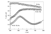
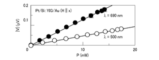
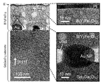
- FIG. 4 is an explanatory view after FIG. 3 of the manufacturing process of the light-spin current conversion element of Example 1 of the present invention. 3 is a TEM image of a cross section of the produced light-spin current conversion element. It is explanatory drawing of the measurement system which investigates a characteristic. It is explanatory drawing of the wavelength dependence of the light transmittance of a sample.
- FIG. 1A is a conceptual perspective view of a light-spin current conversion element according to an embodiment of the present invention.
- the light-spin current conversion element 10 includes a substrate 11, a magnetic layer 12 provided on the substrate 11, an inverse spin Hall effect member layer 13, and surface plasmon resonance generating members 14 1 to 14 3 . I have.
- a pair of electrodes 15 1 and 15 2 for taking out the voltage are provided at both ends of the reverse spin Hall effect member layer 13.
- the magnetization direction of the magnetic layer 12 is defined.
- the surface plasmon resonance generating members 14 1 to 14 3 may be fine metals, prisms, or diffraction gratings. In the case of using a fine metal as a surface plasmon resonance generating member 14 1 may be contained fine metal in the magnetic layer 12, the surface plasmon resonance can be raised magnon effective temperature in the magnetic layer 12.
- the optical fine metal may have any shape and material as long as surface plasmon resonance is caused by irradiation, and is not limited to fine particles, but may be nanowires. From the viewpoint of visible light absorption efficiency and ease of manufacture, gold fine particles or Silver fine particles are preferred. Note that the diameter of the fine particles needs to be sufficiently smaller than the wavelength of the irradiation light, and the plasmon resonance frequency shifts when the diameter or the distance between the particles is changed.
- the fine metal 13 may be formed by forming a metal thin film and then melting it by heating to form fine particles by surface tension, or may be produced using electron beam lithography, or produced and classified in advance. Metal fine particles may be dispersed or may be adsorbed by a self-assembled monolayer.
- a prism as a surface plasmon resonance generating member 14 2 may be provided a prism on the surface of the inverse spin Hall effect member layer 13.
- the surface plasmon can be resonantly excited by the evanescent wave generated when the irradiation light is totally reflected at the interface between the prism and the inverse spin Hall effect member layer, whereby the effective electron temperature in the inverse spin Hall effect member layer 13 is obtained. Can be raised.
- the shape of the prism is arbitrary, but the light incident angle for exciting surface plasmon resonance changes depending on the shape.
- a diffraction grating may be provided on the surface of the inverse spin Hall effect member layer 13, and this diffraction grating is made of the same material as the inverse spin Hall effect member layer 13. May be formed integrally.
- the dispersion line of the diffracted wave reflected by the diffraction grating crosses the dispersion curve of the plasmon, so that the surface plasmon is resonated on the surface of the inverse spin Hall effect member layer.
- the effective electron temperature in the inverse spin Hall effect member layer 13 can be increased.
- the period of the diffraction grating is arbitrary as long as the Bragg-reflected diffracted wave and the plasmon dispersion curve intersect, but the light incident angle for exciting the surface plasmon resonance changes depending on the period.
- the same crystal type GGG Ga 3 Ga 5 O 12
- GGG Ga 3 Ga 5 O 12
- the magnetic material layer 12 may be a thin film magnetic material or a flat magnetic material such as a bulk member.
- the material may be a metal magnetic material, a magnetic semiconductor, or a magnetic dielectric material.
- a prism or a diffraction grating is used as a surface plasmon resonance generating member, it does not matter whether it is conductive. .
- a magnetic dielectric is desirable because the condition for the fine metal to generate surface plasmon resonance is determined by the surrounding dielectric constant.
- the magnetic dielectric material may be anything as long as it contains Fe or Co.
- garnet ferrite, spinel ferrite, or hexagonal ferrite particularly practically, is easily available and has low dissipation of spin angular momentum.
- YIG yttrium iron garnet
- yttrium gallium iron garnet that is, garnet ferrite composed of Y 3 Fe 5-x Ga x O 12 (where 0 ⁇ x ⁇ 5) or YIG Y site It is desirable to use a garnet ferrite substituted with atoms such as Bi, for example, Bi x Y 3-x Fe 5 O 12 .
- Y 3 Fe 5 -x Ga x O 12 has a very large charge gap, so there are no conduction electrons, and therefore the dissipation of spin angular momentum by the conduction electrons is small.
- an inexpensive material such as ordinary ferrite Fe 3 O 4 is desirable from the viewpoint of cost.
- Bi x Y 3-x Fe 5 O 12 when Bi x Y 3-x Fe 5 O 12 is used, the spin current generation efficiency can be increased as compared with YIG.
- a magnetic dielectric such as Y 3 Fe 5-x Ga x O 12 (where 0 ⁇ x ⁇ 5) is used as the magnetic layer 12
- a sputtering method a sputtering method, a MOD method (Metal-organic decomposition method: (Organic metal coating pyrolysis method), sol-gel method, liquid phase epitaxy method, floating zone method, or aerosol deposition method may be used.
- the crystallinity of the magnetic dielectric may be single crystal or polycrystal.
- a MOD solution having a Y 3 Fe 4 GaO 12 composition is applied onto a GGG (Gd 3 Ga 5 O 12 ) single crystal substrate by a spin coating method, for example.
- a spin coating method for example.
- the MOD solution is uniformly applied so that the film thickness after baking becomes 100 nm.
- the MOD solution for example, a MOD solution manufactured by Kojundo Chemical Laboratory Co., Ltd. is used.
- drying is performed on a hot plate heated to 150 ° C. for 5 minutes to evaporate excess organic solvent contained in the MOD solution, and then pre-baking is performed in an electric furnace, for example, at 550 ° C. for 5 minutes. To form an oxide layer.
- crystallization of the oxide layer is advanced in the main baking in which heating is performed at 750 ° C. for 1 to 2 hours in an electric furnace to form a YIG layer.
- the YIG layer may be cut out to a predetermined size.
- aerosol powders of 50 mol%, 27 mol%, and 23 mol% of Fe 2 O 3 , NiO, and ZnO having an average particle diameter of 1 ⁇ m are used. What is necessary is just to deposit Ar gas used as carrier gas at 1000 sccm by jetting it onto the substrate using a nozzle of 0.4 mm ⁇ 10 mm.
- any one of Pt, Au, Pd, Ag, Bi, an element having a transition metal having f or 3d orbit, or an element having any of these alloys is used.
- Bi-doped Cu has a very high generation efficiency of the reverse spin Hall effect.
- the amount of Bi doping in the Bi-doped Cu is suitably about the limit of solid solution in Cu, whereby the spin hole angle (spin current-current conversion efficiency) can be increased five times or more than the value of Pt.
- FIG. 1 (b) is an explanatory view of a mechanism of spin current generation, here, a case where a surface plasmon resonance generating member 14 1 using a fine metal.
- the fine metal (14 1 ) absorbs the light and generates an electron density wave localized on the surface of the fine metal (14 1 ), that is, plasmon. Plasmon generated on the surface of the fine metal (14 1 ) raises the magnon effective temperature due to the plasmon-magnon interaction in the magnetic layer 12.
- FIG. 2 is an explanatory diagram of the characteristics of the light-spin current conversion element according to the embodiment of the present invention.
- Au fine particles are used as the fine metal (14 1 )
- Bi: YIG is used as the magnetic layer 12
- reverse spin is performed. It is a characteristic view when Pt is used as the Hall effect member layer and the application direction of the external magnetic field is 90 ° with respect to the opposing direction of the electrodes.
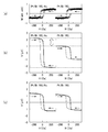
- FIG. 2 (a) is an explanatory diagram of the magnetization process, and the same hysteresis curve is obtained both when the Au fine particles are contained and when no Au fine particles are contained. It was not seen.
- FIG. 2B is an explanatory view of the electromotive force V when 350 mW of white light is irradiated. Regardless of the presence or absence of Au fine particles, the sign of all the electromotive force signals is inverted due to the magnetic field inversion. It was confirmed that the symmetry of the spin Hall effect was satisfied. However, the inclusion of Au fine particles increases the electromotive force signal by a factor of about 2 compared to the case of not containing Au, and it is interpreted that the Au fine particles absorb light and plasmons are generated on the surface thereof. .
- the characteristics of the sample containing no Au fine particles shown in FIG. 2B are considered to be due to the spin Seebeck effect based on heat generation due to light absorption, and the characteristics of the sample containing Au fine particles are the electromotive force due to plasmon and the spin Seebeck effect. It will be by hybrid power generation.
- the effective electron temperature T * e, P in the inverse spin Hall effect member layer 13 is greater than the effective magnon temperature T * m, F in the magnetic layer 12. Therefore, the backflow spin current J fl becomes larger than the spin pumping spin current J sp , and the difference (J fl ⁇ J sp ) is induced in the inverse spin Hall effect member layer 13 as the spin current J s .
- the light-spin current conversion element of Example 1 of the present invention will be described.
- 3 and 4 are explanatory views of the manufacturing process of the light-spin current conversion element of Example 1 of the present invention.
- the ⁇ 111 ⁇ plane is the main surface.
- An Au film 22 having a thickness of 5 nm is deposited on a GGG (Gd 3 Ga 5 O 12 ) single crystal substrate 21.
- the film is heated to 1000 ° C. in an air atmosphere, and the Au film 22 is melted and converted into Au fine particles 23 using surface tension.
- the average diameter of the Au fine particles 23 is about 70 nm, which is a size sufficiently smaller than the wavelength for visible light. It should be noted that the density of the Au fine particles 23 can be increased by repeating the thin film deposition and fine particle processes. By increasing the density of the Au fine particles 23, the light absorption efficiency and the spin current generation efficiency can be improved.
- a MOD solution having a Bi 1 Y 2 Fe 4 GaO 12 composition is applied by spin coating.
- the MOD solution 24 is uniformly applied so that the film thickness after baking is 100 nm by rotating at 5000 rpm for 60 seconds.
- drying is performed on a hot plate heated to 50 ° C. for 5 minutes to evaporate excess organic solvent contained in the MOD solution 24. Then, in an electric furnace, for example, the oxide layer 25 is formed by temporary baking at 60 ° C. for 60 minutes.
- crystallization of the oxide layer 25 is advanced in the main firing in which heating is performed at 725 ° C. for 10 hours in an electric furnace to obtain an Au-containing Bi: YIG layer 26.
- the Au-containing Bi: YIG layer 26 is cut out to a size of 10 mm ⁇ 5 mm.
- a Pt film 27 having a thickness of 15 nm is formed on the surface of the Au-containing Bi: YIG layer 26.
- a pair of electrodes 28 1 and 28 2 are formed on both ends of the Pt film 27.
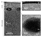
- FIG. 5 is a TEM image of the cross section of the actually produced light-spin current conversion element. It can be seen that Au fine particles having a size of about 70 nm are embedded in Bi: YIG.
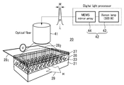
- FIG. 6 is an explanatory diagram of a measurement system for examining characteristics, and the light-spin current conversion element 20 is irradiated with light from the digital optical processor 42 via the optical fiber 41.
- the digital light processor 42 includes a light source 43 and a spectroscopic optical system 44.
- a 500 W xenon lamp that generates white light in the wavelength range of 390 nm to 770 nm is used as the light source 43
- a MEMS mirror array is used as the spectroscopic optical system 44
- monochromatic light with a bandwidth of 20 nm is spectrally irradiated.
- the light intensity is 350 mW as white light and is less than 20 mW as monochromatic light.
- the magnetic field H is applied as the magnetic field applying means 29 using a permanent magnet.
- FIG. 7 is an explanatory diagram of the wavelength dependence of the light transmittance of the sample, and shows the measurement results for Pt film, Au fine particle-free Pt / Bi: YIG, and Au fine particle-containing Pt / Bi: YIG / Au. ing.
- Pt / Bi YIG / Au
- a minimum point of light transmittance is observed at a wavelength of about 700 nm due to the influence of light absorption characteristics of Au fine particles.
- FIG. 8 is an explanatory diagram of the wavelength dependence of the electromotive force in the Pt layer.
- the measurement was performed with an external magnetic field applied.
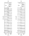
- FIG. 10 is an explanatory diagram of the magnetic field dependence of the electromotive force in the Pt layer
- FIG. 10A is a characteristic diagram of Pt / Bi: YIG / Au containing Au fine particles
- FIG. It is a characteristic view of Pt / Bi: YIG not containing Au fine particles.
- an electromotive force is also generated in Pt / Bi: YIG that does not contain Au fine particles. This is an electromotive force due to the spin Seebeck effect due to the heat generation of the sample due to light absorption. It is.
- FIG. 11 is a TEM image of a cross section of a sample with voids prepared for comparison. It can be seen that Au fine particles having a size of about 50 nm are embedded in Bi: YIG, and voids are generated on both sides of the Au fine particles.
- FIG. 12 is an explanatory diagram of the wavelength dependence of the light transmittance of a sample prepared for comparison, and shows the measurement results for Pt / Bi: YIG / Au containing Au fine particles with voids.
- Pt / Bi YIG / Au with voids
- a minimum point of light transmittance is observed at a wavelength of about 630 nm due to the influence of light absorption characteristics of Au fine particles.
- FIG. 13 is an explanatory diagram of the wavelength dependence of the electromotive force in the Pt layer of a sample prepared for comparison.
- FIG. 14 is an explanatory diagram of the wavelength dependence of the light transmittance of a sample using Au instead of Pt. Similar to the case of using Pt, the wavelength is about 670 nm under the influence of the light absorption characteristics of Au fine particles. The minimum point of light transmittance (maximum point of light absorption rate) can be seen.
- FIG. 15 is an explanatory diagram of the wavelength dependence of the electromotive force in the Au layer of a sample using Au instead of Pt.
- monochromatic light with a bandwidth of 20 nm to ⁇ 20 mW is irradiated and the pair of electrodes are opposed to each other.
- Bi YIG contains Au fine particles that can absorb light by plasmon resonance, so that spin current can be generated by light
- Bi YIG Since Pt, which is an inverse spin Hall effect member, is bonded to the substrate, a photovoltaic element can be obtained by providing a pair of electrodes on Pt.
- this light-spin current conversion element is basically a hybrid power generation of heat and light
- a simple spin-Seebeck is used when attached to a waste heat source under sunlight or illumination light.
- the output can be made larger than the effect and the light-spin current conversion effect.
- Example 1 since the fine particles are formed by molten Au, the Au fine particles have a single layer structure. However, the Au fine particle preparation process and the Bi: YIG film formation process are alternately repeated a plurality of times. By dispersing the formed Au fine particles in the MOD solution, the Au fine particles can be uniformly and densely dispersed in Bi: YIG.
- Example 2 of the present invention the light-spin current conversion element of Example 2 of the present invention will be described.
- the light-spin current conversion element of Example 2 is the same as that of Example 1 described above.
- An antiferromagnetic layer as a magnetic field applying means is joined to the flow conversion element.
- FIG. 16 is a conceptual perspective view of the light-spin current conversion element of Example 2 of the present invention.
- an IrMn layer 30 as an antiferromagnetic material layer on the GGG substrate 21 by the sputtering method
- FIG. As in the first embodiment, the Au-containing Bi: YIG layer 26 and the Pt film 27 are formed, and a pair of electrodes 28 1 and 28 2 for extracting voltage are provided on both ends of the Pt film 27.
- the IrMn layer 30 which is an antiferromagnetic material layer is used as the magnetic field applying means, and the magnetization direction is perpendicular to the opposing direction of the pair of electrodes 28 1 and 28 2. And the magnetic field H is applied.
- the magnetic field applying means is provided in the light-spin current conversion element itself, it is not necessary to set the magnetic field applying means outside, for example, when the device is mounted on a portable device. In addition, power can be easily generated as long as there is light in the environment.
- the light-spin current conversion element of Example 3 of the present invention uses an optical prism as a surface plasmon resonance generating member. It is what was used.
- FIG. 17 is a conceptual perspective view of the light-spin current conversion element according to the third embodiment of the present invention.
- a Bi: YIG layer 31 and a Pt film 27 are formed on the GGG substrate 21, and both ends of the Pt film 27 are formed.
- a pair of electrodes 28 1 and 28 2 for voltage extraction are provided.
- the optical microprism 32 is bonded to one end side of the Pt film 27.
- the surface plasmon can be resonantly excited by the evanescent wave generated at that time, whereby the Pt film 27
- the effective electron temperature can be increased.
- the light-spin current conversion element of Example 4 of the present invention will be described with reference to FIG. 18.
- the light-spin current conversion element of Example 3 has a diffraction grating as a surface plasmon resonance generating member. It is what was used.
- FIG. 18 is a conceptual perspective view of the light-spin current conversion element of Example 4 of the present invention, in which a Bi: YIG layer 31 and a Pt film 27 are formed on the GGG substrate 21.
- an Au film is formed, a resist is applied, a diffraction grating pattern is formed by electron beam lithography or the like, and then the exposed portion of the Au film is etched by sputter etching to form the diffraction grating 33.
- a resist may be applied before forming the Au film, and after forming a diffraction grating pattern by electron beam lithography or the like, the Au film may be formed, and the diffraction grating 33 may be formed by a lift-off method.
- a pair of electrodes 28 1 and 28 2 for voltage extraction are provided at both ends of the Pt film 27.
- the dispersion line of the diffracted wave reflected by the diffraction grating 33 intersects with the plasmon dispersion curve, so that surface plasmons are resonantly excited on the surface of the Pt film 27. be able to.
- the light-spin current conversion element of Example 5 of the present invention is a reverse spin Hall as a surface plasmon resonance generating member. A diffraction grating integrated with the effect member layer is used.
- FIG. 19 is a conceptual perspective view of the light-spin current conversion element of Example 5 of the present invention.
- a Bi: YIG layer 31 is formed on the GGG substrate 21, a thick Au film is formed.
- sputter etching is performed to etch the surface of the exposed portion of the Au film to form the diffraction grating 34, and the lower Au film is used as an inverse spin Hall effect member layer 35.
- Example 5 the mechanism for obtaining the electromotive force is the same as that of Example 4 described above.
- a resist is applied before forming the Au film, and after forming the diffraction grating pattern by electron beam lithography or the like, the Au film is formed and lift-off is performed.
- the diffraction grating 33 may be formed by a method.
Landscapes
- Physics & Mathematics (AREA)
- General Physics & Mathematics (AREA)
- Optics & Photonics (AREA)
- Hall/Mr Elements (AREA)
- Thin Magnetic Films (AREA)
Abstract
光-スピン流変換素子及びその製造方法に関し、新規なスピン流源を提供する。磁性体層と、前記磁性体層に接合する逆スピンホール効果部材層と、照射光による表面プラズモン共鳴により前記磁性体層のマグノン有効温度或いは逆スピンホール効果部材層の電子有効温度の少なくとも一方を高める表面プラズモン共鳴発生部材とを設ける。
Description
本発明は、光-スピン流変換素子及びその製造方法に関するものであり、例えば、可視光等の光を磁性体部材で吸収し、光のエネルギーでマグノン有効温度若しくは電子有効温度を上昇させてスピン流に変換する構成に特徴のある光-スピン流変換素子及びその製造方法に関するものである。
現在の半導体装置等のエレトロニクス分野においては、電子の有する電荷の自由度を利用しているが、電子は電荷以外にスピンという自由度を有している。近年、このスピンの自由度を利用したスピントロニクスが次世代の情報技術の担い手として注目を集めている。
このスピントロニクスでは電子の電荷とスピンの自由度を同時に利用することによって、従来にない機能や特性を得ることを目指しているが、スピントロニクス機能の多くはスピン流によって駆動される。
スピン流はエネルギーの散逸が少ないため、効率の良いエネルギー伝達に利用できる可能性が期待されており、スピン流の生成方法や検出方法の確立が急務になっている。
なお、スピン流の生成方法としては、スピンポンピングによるスピン流が提案されており(例えば、非特許文献1参照)、スピン流の検出方法についても、本発明者等により逆スピンホール効果(ISHE)によるスピン流の検出方法が提案されている(例えば、非特許文献2参照)。
さらに、本発明者は、熱をスピン流の発生源としたスピン-ゼーベック効果素子(例えば、特許文献1参照)や、音波発生部材を用いた音波-スピン流変換素子(例えば、非特許文献3或いは非特許文献4参照)や、マイクロ波をスピン流に変換するマイクロ波-スピン流変換素子(例えば、非特許文献5参照)を提案している。
本発明者等による鋭意研究の結果、このようなスピン流は、磁性体層のマグノン有効温度(T*
m,F)と磁性体層と界面で接する金属層の電子有効温度(T*
e,P)との間に差をつけることによって発生することが解明された。
図20は、スピン流発生メカニズムの説明図であり、図20(a)はT*
m,F=T*
e,Pの場合、図20(b)はT*
m,F>T*
e,Pの場合、図20(c)はT*
m,F<T*
e,Pの場合のスピン流の説明図である。
スピンには非相反性があるため、右回りにしか歳差運動しないので、スピンに熱揺らぎが加わると一方向に偏った歳差運動が生じ、スピンポンピングを介してスピン流が生成される。磁性体/金属界面においては、磁性層の磁気モーメントに対する熱揺らぎによるスピンポンピングスピン流Jsp(マグノン温度に比例)と金属層の電子スピンに対する熱揺らぎによるバックフロースピン流Jfl(電子温度に比例)が生成される。
図20(a)に示すように、熱平衡状態では、環境温度=マグノン温度=電子温度であるので、スピンポンピングスピン流Jspとバックフロースピン流Jflとは吊り合った状態になるので正味のスピン流は生成されない。
逆に言えば、外部入力を印加してスピンポンピングスピン流Jspとバックフロースピン流Jflとのバランスを崩せば、スピンポンピングスピン流Jspとバックフロースピン流Jflの差分が正味のスピン流となるので、図20(b)或いは図20(c)に示すように、有限のスピン流を生成することができる。特に、図20(b)に示すように、磁性体層のマグノン有効温度T*
m,Fを金属層の電子有効温度T*
e,Pより大きくすると、金属層にスピン流Jsを誘起することができる。
このような関係を纏めたのが下記の式である。
Js=2αkB(T* m,T-T* e,T)
ここで、αは、有効温度差-スピン流変換係数であり、kBはボルツマン定数である(例えば、非特許文献6参照)。
Js=2αkB(T* m,T-T* e,T)
ここで、αは、有効温度差-スピン流変換係数であり、kBはボルツマン定数である(例えば、非特許文献6参照)。
したがって、磁性体層におけるマグノン有効温度を高めることによって、磁性体層と界面で接する金属層にスピン流を誘起することができる。この時、金属層として逆スピンホール効果部材を用い、外部磁場を印加すると外部磁場と直交する方向に逆スピンホール電圧EISHEが発生する。
Phys.Rev.,B19,p.4382,1979
Applied Physics Letters Vol.88,p.182509,2006
Nature Mater.,Vol.10,No.10,p.737,2011
Appl.Phys.Lett.,Vol.99,No.21,p.212501,2011
Nature Mater.,Vol.10,No.9,p.655,2011
Nature Mater.,Vol.9,No.11,p.894,2010
しかし、上述のスピン流発生方法では、材料や組成構成が限定されてしまい、且つ、スピン流を発生させる外部エネルギーの種類も限られており、素子設計の自由度という観点からは必ずしも十分なものではなかった。
例えば、近年、さまざまな自然界のエネルギーを電気に変えて利用する環境発電(エネルギーハーベスティング)技術が注目を集めている。この環境発電とは、自然界や他の仕事で使われているエネルギーの廃棄分を、電気エネルギーとして「収穫」あるいは「落ち穂拾い」のように回収するものである。
従来の環境発電においては、ゼーベック効果素子により廃熱からエネルギーを回収したり或いは機械の振動を利用した発電等が試みられているが、実際に試みられている例では利用するエネルギー源が限られているという問題がある。
したがって、本発明は、光源からプラズモンを発生させてスピン流を生成する新規なスピン流源を提供することを目的とする。
上記課題を解決するために、本発明は、光-スピン流変換素子であって、磁性体層と、前記磁性体層に接合する逆スピンホール効果部材層と、照射光による表面プラズモン共鳴により前記磁性体層のマグノン有効温度或いは逆スピンホール効果部材層の電子有効温度の少なくとも一方を高める表面プラズモン共鳴発生部材とを有する。
このように、照射光により表面プラズモン共鳴を発生させる表面プラズモン共鳴発生部材を設けることにより、光照射によって、磁性体層のマグノン有効温度或いは逆スピンホール効果部材層の電子有効温度の少なくとも一方を高めることができ、金属層中にスピン流を誘起することができる。なお、前記磁性体層の磁化方向を規制する磁場印加手段は、基板に磁化した反強磁性体を接合しても良いし或いは、電磁コイル或いは永久磁石として素子の外部に設けても良い。
この場合の表面プラズモン共鳴発生部材としては、前記磁性体層に含ませた微細金属を用いても良い。なお、微細金属は、照射光により表面プラズモン共鳴が起こるサイズであれば、形状及び素材は任意であり、微粒子に限らずナノワイヤでも良いが、可視光吸収効率や製造容易性の観点からは、金微粒子或いは銀微粒子が好適である。
また、表面プラズモン共鳴発生部材としては、逆スピンホール効果部材層の表面に設けられたプリズム或いは逆スピンホール効果部材層の表面に設けられた回折格子を用いても良い。なお、回折格子を用いる場合には、逆スピンホール効果部材層と同じ材料で一体に形成しても良い。
また、逆スピンホール効果部材層に、印加する外部磁場と直交する方向に一対の電極を設けることによって、逆スピンホール効果により電圧を取り出すことができる。
また、磁性体層としては、原理的には金属磁性体でも良いが、実際に表面プラズモン共鳴を起こすためには、表面プラズモン共鳴条件は微細金属の周囲の媒質の誘電率に依存するので、絶縁性磁性体であるY3Fe5-xGaxO12(但し、0≦x<5)またはBiドープのY3Fe5-xGaxO12(但し、0≦x<5)が望ましい。
また、逆スピンホール効果部材層としては、Pt、Au、Pd、Ag、Bi、f軌道或いは3d軌道を有する遷移金属を有する元素、若しくはそれらの合金のいずれかを有する元素のいずれか、或いは、前記各材料とCu、Al、或いは、Siの合金のいずれかであることが望ましい。特に、逆スピンホール効果の生成効率の高いPt或いはBiドープCuが望ましい。
また、本発明は、光-スピン流変換素子の製造方法であって、基板上に金属薄膜を堆積する工程と、熱処理により前記金属膜を溶融して表面張力により微細金属を形成する工程と、前記微細金属を含む基板上に磁性体部材を堆積して微細金属を含有する磁性体層を形成する工程と、前記磁性体層上に逆スピンホール効果部材層を形成する工程とを有する。
このように、金属膜を溶融して表面張力により微細金属を形成する工程を設けることによって、微細金属のサイズは、金属薄膜の膜厚と熱処理の温度により容易に制御することができる。
開示の光-スピン流変換素子及びその製造方法によれば、表面プラズモン共鳴を利用することによって、磁性体層のマグノン有効温度或いは逆スピンホール効果部材層の電子有効温度の少なくとも一方を上昇させることがき、それによって、新規なスピン流源を提供することができる。
ここで、図1及び図2を参照して、本発明の実施の形態を説明する。図1(a)は、本発明の実施の形態の光-スピン流変換素子の概念的斜視図である。図に示すように、光-スピン流変換素子10は、基板11と、基板11上に設けた磁性体層12と、逆スピンホール効果部材層13と表面プラズモン共鳴発生部材141~143を備えている。また、逆スピンホール効果部材層13から起電力を取り出す場合には、逆スピンホール効果部材層13の両端に電圧取り出し用の一対の電極151,152とを設ける。また、磁場印加手段16を設けることによって、磁性体層12の磁化方向を規定する。
表面プラズモン共鳴発生部材141~143は、微細金属でも、プリズムでも或いは回折格子でも良い。表面プラズモン共鳴発生部材141として微細金属を用いる場合には、微細金属を磁性体層12中に含有させれば良く、表面プラズモン共鳴により磁性体層12におけるマグノン有効温度を上昇させることができる。
光微細金属は、照射により表面プラズモン共鳴が起こるサイズであれば、形状及び素材は任意であり、微粒子に限らずナノワイヤでも良いが、可視光吸収効率や製造容易性の観点からは、金微粒子或いは銀微粒子が好適である。なお、微粒子の直径は照射光の波長よりも十分に小さい必要があり、また、直径や粒子間距離を変えるとプラズモン共鳴周波数がシフトする。なお、微細金属13は、金属薄膜を成膜したのち、加熱により溶融させて表面張力により微粒子化をしても良いし、電子線リソグラフィーを用いて作製しても良いし、予め作製し分級した金属微粒子を散布したり、自己組織化単分子膜で吸着させたりしても良い。
また、表面プラズモン共鳴発生部材142としてプリズムを用いる場合には、逆スピンホール効果部材層13の表面にプリズムを設ければ良い。照射光がプリズムと逆スピンホール効果部材層との界面で全反射する時に発生するエバネッセント波により表面プラズモンを共鳴的に励起することができ、それによって、逆スピンホール効果部材層13における電子有効温度を上昇させることができる。プリズムを用いる場合、プリズムの形状は任意であるが、形状に依存して表面プラズモン共鳴を励起するための光入射角が変化する。
また、表面プラズモン共鳴発生部材143として回折格子を用いる場合には、逆スピンホール効果部材層13の表面に回折格子を設ければ良く、この回折格子は逆スピンホール効果部材層13と同じ材料で一体に形成しても良い。照射光が回折格子に照射されると、回折格子によってブラッグ反射された回折波の分散直線がプラズモンの分散曲線と交差するようになるので、逆スピンホール効果部材層の表面に表面プラズモンを共鳴的に励起することができ、それによって、逆スピンホール効果部材層13における電子有効温度を上昇させることができる。回折格子の周期は、ブラッグ反射された回折波とプラズモンの分散曲線が交差する範囲であれば任意であるが、周期に依存して表面プラズモン共鳴を励起するための光入射角が変化する。
この場合の基板11としては、磁性体層12を単結晶或いは単結晶に近い結晶状態にするには、磁性体層12として、YIG等を用いる場合には同じ結晶型であるGGG(Gd3Ga5O12)単結晶等のガーネット基板等が望ましい。
磁性体層12は、薄膜磁性体でも或いはバルク部材等の平板状の磁性体でも良い。また、材質としては、原理的には、金属磁性体でも、磁性半導体でも、或いは、磁性誘電体でも良く、表面プラズモン共鳴発生部材としてプリズム或いは回折格子を用いる場合には導電性の如何を問わない。但し、表面プラズモン共鳴発生部材として微細金属を用いる場合には、微細金属が表面プラズモン共鳴を発生するための条件は周囲の誘電率で決まるので磁性誘電体が望ましい。
磁性誘電体としては、FeやCoを含むものであれば何でも良いが、ガーネットフェライト、スピネルフェライト、或いは、六方晶フェライト、特に、実用的には、入手が容易で且つスピン角運動量の散逸の小さいYIG(イットリウム鉄ガーネット)やイットリウムガリウム鉄ガーネット、即ち、一般式で表記するとY3Fe5-xGaxO12(但し、0≦x<5)からなるガーネットフェライト、或いは、YIGのYサイトをBi等の原子で置換したガーネットフェライト、例えば、BixY3-xFe5O12等を用いることが望ましい。
これは、Y3Fe5-xGaxO12は電荷ギャップが非常に大きいので伝導電子が存在せず、したがって、伝導電子によるスピン角運動量の散逸が小さいためである。但し、コストの観点からは、通常のフェライトFe3O4等の安価な材料が望ましい。特に、BixY3-xFe5O12を用いた場合には、YIGに比べてスピン流生成効率を高めることができる。
また、磁性体層12の磁化方向を固定するための磁場印加手段16は、コイル等を使用した外部磁場印加機構でも、或いは、ピン止め層となる反強磁性体を用いても良い。なお、逆スピンホール効果により発生する起電力EISHEは発生したスピン流jSとスピン偏極方向の外積方向に生じるので、磁場印加方向は、逆スピンホール効果部材層13の長手方向に対して垂直方向θ=90°とすることが望ましい。
また、磁性体層12として、Y3Fe5-xGaxO12(但し、0≦x<5)等の磁性誘電体を用いる場合には、スパッタ法、MOD法(Metal-organic decomposition Method:有機金属塗布熱分解法)、ゾル-ゲル法、液相エピタキシー法、フローティングゾーン法、或いは、エアロゾルデポジッション法のいずれを用いても良い。また、磁性誘電体の結晶性としては単結晶でも良いし或いは多結晶でも良い。
MOD法を用いる場合には、例えば、GGG(Gd3Ga5O12)単結晶基板上に、例えば、Y3Fe4GaO12組成のMOD溶液をスピンコート法で塗布する。この場合のスピンコート条件としては、まず、500rpmで5秒間回転させたのち、3000~4000rpmで30秒間回転させてMOD溶液を焼成後の膜厚が100nmになるように均一に塗布する。なお、MOD溶液としては、例えば、(株)高純度化学研究所製のMOD溶液を用いる。
次いで、例えば、150℃に加熱したホットプレート上で5分間乾燥させて、MOD溶液に含まれる余分な有機溶媒を蒸発させ、次いで、電気炉中において、例えば、550℃で5分間加熱する仮焼成によって酸化物層とする。
次いで、電気炉中において、750℃で1~2時間加熱する本焼成において酸化物層の結晶化を進めてYIG層とする。最後に、YIG層を所定のサイズに切り出せば良い。
また、エアロゾルデポジション法を用いる場合には、例えば、平均粒径が1μmのFe2O3、NiO,ZnOそれぞれ、50mol%、27mol%、23mol%のエアロゾル用粉体を用い、例えば、開口が0.4mm×10mmのノズルを用いてキャリアガスとなるArガスを1000sccm流して基板上に噴射させて堆積させれば良い。
また、逆スピンホール効果部材層13としては、Pt、Au、Pd、Ag、Bi、或いは、f軌道或いは3d軌道を有する遷移金属を有する元素、若しくはそれらの合金のいずれかを有する元素のいずれか、或いは、これらの材料とCu、Al、或いは、Siの合金を用いることが望ましい。前者の元素、特に、Ptはスピン軌道相互作用が大きいので、生成されたスピン流を高効率に起電力に変換することができる。
但し、コストの観点からは、前者の材料とCu、Al、或いは、Siの合金が望ましく、特に、BiドープのCuは逆スピンホール効果の生成効率が非常に高い。なお、BiドープCuにおけるBiドープ量はCu中への固溶限界程度が適当であり、これによりスピンホール角(スピン流-電流変換効率)をPtの値よりも5倍以上高めることができる。
図1(b)はスピン流発生のメカニズムの説明図であり、ここでは、表面プラズモン共鳴発生部材141として微細金属を用いた場合を示している。光を照射すると微細金属(141)が光を吸収して微細金属(141)の表面に局在する電子密度の波、即ち、プラズモンを発生する。微細金属(141)の表面で発生したプラズモンは、磁性体層12の中におけるプラズモン-マグノン相互作用により、マグノン有効温度を上昇させる。
磁性体層12のマグノン有効温度が、逆スピンホール効果部材層13の中の電子有効温度より高くなると、磁性体層12にスピン流が発生して、逆スピンホール効果部材層13に界面から垂直方向にスピン流がポンピングされる。一方、磁場印加手段16により、磁性体層12はHの方向に磁化されているので、逆スピンホール効果部材層13におけるスピン偏極方向σはH方向或いは-H方向になる。起電力EISHEは、
EISHE∝jS×σ
を満たす方向に発生するため、逆スピンホール効果部材層13において磁場Hと直交する方向に電流Jcが発生する。
EISHE∝jS×σ
を満たす方向に発生するため、逆スピンホール効果部材層13において磁場Hと直交する方向に電流Jcが発生する。
図2は、本発明の実施の形態の光-スピン流変換素子の特性の説明図であり、微細金属(141)としてAu微粒子を用い、磁性体層12としてBi:YIGを用い、逆スピンホール効果部材層としてPtを用い、外部磁場の印加方向を電極の対向方向に対して90°とした場合の特性図である。
図2(a)は、磁化過程の説明図であり、Au微粒子を含有させた場合も、Au微粒子を含有しない場合にも同様のヒステリシス曲線が得られ、Au微粒子の有無により磁化特性に変化はみられなかった。
図2(b)は、350mWの白色光を照射した場合の起電力Vの説明図であり、Au微粒子の有無にかかわらず、全ての起電力信号が磁場反転により符号が反転しており、逆スピンホール効果の対称性を満たしていることが確認された。しかし、Au微粒子を含有させることによって、非含有の場合に比べて起電力信号が2倍程度大きくなっており、Au微粒子が光を吸収してその表面にプラズモンが発生していると解釈される。
図2(c)は、基板側を298Kとし、Pt側を300Kとし、基板とPt膜との間の温度差をΔT=2°としてスピンゼーベック効果の測定結果を示した図である。図に示すように、Au微粒子の有無に拘らずほぼ同程度の起電力信号が得られた。
したがって、図2(b)に示したAu微粒子非含有の試料の特性は光吸収による発熱に基づくスピンゼーベック効果によるものと考えられ、Au微粒子含有の試料の特性はプラズモンによる起電力とスピンゼーベック効果のハイブリッド発電によるものになる。
なお、表面プラズモン共鳴発生部材としてプリズム或いは回折格子を用いた場合には、逆スピンホール効果部材層13における電子有効温度T*
e,Pが磁性体層12におけるマグノン有効温度T*
m,Fより高くなるので、バックフロースピン流Jflの方がスピンポンピングスピン流Jspより大きくなり、その差分(Jfl-Jsp)がスピン流Jsとして逆スピンホール効果部材層13に誘起される。
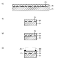
ここで、図3乃至図10を参照して、本発明の実施例1の光-スピン流変換素子を説明する。図3及び図4は、本発明の実施例1の光-スピン流変換素子の製造工程の説明図であり、まず、図3(a)に示すように、{111}面を主面とするGGG(Gd3Ga5O12)単結晶基板21上に、厚さが5nmのAu膜22を蒸着する。
次いで、図3(b)に示すように、大気雰囲気中で1000℃に加熱し、Au膜22を溶融して表面張力を利用してAu微粒子23に変換する。この場合のAu微粒子23の平均直径は70nm程度になり、可視光に波長に比べて十分小さいサイズになる。なお、薄膜蒸着と微粒子化のプロセスを繰り返すことにより、Au微粒子23の密度を高めることができる。Au微粒子23を高密度化することにより、光吸収効率及びスピン流生成効率を向上させることができる。
次いで、図3(c)に示すように、例えば、Bi1Y2Fe4GaO12組成のMOD溶液をスピンコート法で塗布する。この場合のスピンコート条件としては、5000rpmで60秒間回転させてMOD溶液24を焼成後の膜厚が100nmになるように均一に塗布する。
次いで、図3(d)に示すように、例えば、50℃に加熱したホットプレート上で5分間乾燥させて、MOD溶液24に含まれる余分な有機溶媒を蒸発させ、次いで、電気炉中において、例えば、480℃で60分間加熱する仮焼成によって酸化物層25とする。
次いで、図4(e)に示すように、電気炉中において、725℃で10時間加熱する本焼成において酸化物層25の結晶化を進めてAu含有Bi:YIG層26とする。次いで、図4(f)に示すように、Au含有Bi:YIG層26を10mm×5mmのサイズに切り出す。
次いで、図4(g)に示すように、Au含有Bi:YIG層26の表面に厚さが15nmのPt膜27を形成する。最後に、図4(h)に示すように、Pt膜27の両端に一対の電極281,282を形成する。
図5は、実際に作製した光-スピン流変換素子の断面のTEM像であり、70nm程度のサイズのAu微粒子がBi:YIGに埋め込まれているのが分かる。
図6は、特性を調べる測定系の説明図であり、光-スピン流変換素子20に光ファイバ41を介してデジタル光プロセッサ42から光を照射する。デジタル光プロセッサ42は光源43と分光光学系44を備えている。ここでは、光源43として390nm~770nmの波長範囲の白色光を発生する500Wのキセノンランプを用い、分光光学系44としては、MEMSミラーアレイを用い、バンド幅が20nmの単色光に分光して照射する。光強度は白色光として350mWであり、分光した単色光としては20mW未満となる。なお、ここでは、磁場印加手段29として永久磁石を用いて磁場Hを印加している。
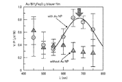
図7は、試料の光透過率の波長依存性の説明図であり、Pt膜、Au微粒子非含有のPt/Bi:YIG、Au微粒子含有のPt/Bi:YIG/Auについての測定結果を示している。Pt/Bi:YIG/Auの場合には、Au微粒子の光吸収特性の影響を受けて、700nm程度の波長で光透過率の極小点(光吸収率の極大点)が見られる。
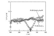
図8は、Pt層における起電力の波長依存性の説明図であり、ここでは、バンド幅20nmで~20mWの単色光を照射するとともに、一対の電極の対向方向に直交する方向にH=200Oeの外部磁場を印加した状態で測定を行った。
図に示すように、Au微粒子非含有のPt/Bi:YIGの場合には、波長依存性はほとんど見られないのに対して、Au微粒子含有のPt/Bi:YIG/Auの場合には、光吸収波長の極大点に対応する位置に出力ピークが見られた。なお、Au微粒子含有のPt/Bi:YIG/Auに対して一対の電極の対向方向と平行に外部磁場を印加した場合には、一対の電極の対向方向には逆スピンホール効果による起電力は発生しないので出力はほぼ0であった。
図9は、Pt層における起電力の光強度依存性の説明図であり、λ=690nmの場合もλ=500nmの場合にも、起電力は照射光強度に対してほぼリニアに増大する。
図10は、Pt層における起電力の磁場依存性の説明図であり、図10(a)は、Au微粒子含有のPt/Bi:YIG/Auの特性図であり、図10(b)は、Au微粒子非含有のPt/Bi:YIGの特性図である。ここでは、バンド幅を20nmとし、λ=400nmからλ=760nmまでの単色光を順次照射した。
図10(b)に示すように、Au微粒子非含有のPt/Bi:YIGにも、起電力が発生しているが、これは、光吸収により試料が発熱したことによるスピンゼーベック効果による起電力である。
一方、図10(a)に示すように、Au微粒子含有のPt/Bi:YIG/Auの場合には、より大きな起電力が発生しており、これは、プラズモン共鳴による起電力がスピンゼーベック効果による起電力に加わったものである。
即ち、これは最近の研究の進展で明らかになった点であるが、Pt層が単に温まった場合(Pt層の「格子」温度が上昇した場合)、温度勾配に伴うフォノンの長距離伝播によってPt層の電子温度は逆に低下する。YIG/Pt界面ではYIGのマグノン温度の方がPt層の電子温度よりも高くなるため、YIGからPtにスピン流が流れる。プラズモン共鳴時には、プラズモン-マグノン相互作用によりマグノン温度が高くなるため、この場合もYIGからPtにスピン流が流れる。したがって、Au微粒子含有のPt/Bi:YIG/Auの場合には、発熱成分とプラズモン成分が同じ符号の逆スピンホール電圧を与えることになる。
次に、図11乃至図13を参照して、ボイドのある試料を比較のために作成したので説明する。図11は比較のために作成したボイドのある試料の断面のTEM像である。50nm程度のサイズのAu微粒子がBi:YIGに埋め込まれており、Au微粒子の両側にボイドが発生しているのが分かる。
図12は、比較のために作成した試料の光透過率の波長依存性の説明図であり、ボイドのあるAu微粒子含有のPt/Bi:YIG/Auについての測定結果を示している。ボイドのあるPt/Bi:YIG/Auの場合には、Au微粒子の光吸収特性の影響を受けて、630nm程度の波長で光透過率の極小点(光吸収率の極大点)が見られる。
図13は、比較のために作成した試料のPt層における起電力の波長依存性の説明図であり、ここでも、バンド幅20nmで~20mWの単色光を照射するとともに、一対の電極の対向方向に直交する方向にH=200Oeの外部磁場を印加した状態で測定を行った。
図に示すように、Au微粒子非含有のPt/Bi:YIGの場合には、波長依存性はほとんど見られないのに対して、ボイドのあるAu微粒子含有のPt/Bi:YIG/Auの場合には、光吸収波長の極大点に対応する位置に出力ピークではなくディップ信号が見られた。表面プラズモンにより誘起された電磁場はAu微粒子近傍に局在しているため、Bi:YIGとAuの間にボイドによる隙間があるとプラズモン誘起スピン流による正符号の電圧は発生しないことを示している。
このボイドのある試料では、光吸収に伴うAu微粒子の発熱によって温度分布が変わり、スピンゼーベック効果によるバックグラウンド信号が変化し、上述のように、プラズモン共鳴点で、ピークではなく、ディップ信号が生じることになる。
次に、図14及び図15を参照して、逆スピンホール効果部材としてPtの代わりにAuを用いた場合の特性を説明する。図14はPtの代わりにAuを用いた試料の光透過率の波長依存性の説明図であり、Ptを用いた場合と同様にAu微粒子の光吸収特性の影響を受けて、670nm程度の波長で光透過率の極小点(光吸収率の極大点)が見られる。
図15はPtの代わりにAuを用いた試料のAu層における起電力の波長依存性の説明図であり、ここでも、バンド幅20nmで~20mWの単色光を照射するとともに、一対の電極の対向方向に直交する方向にH=200Oeの外部磁場を印加した状態で測定を行った。
図に示すように、Au微粒子非含有のAu/Bi:YIGの場合には、波長依存性はほとんど見られないのに対して、Au微粒子含有のAu/Bi:YIG/Auの場合には、光吸収波長の極大点に対応する位置に出力ピークが見られた。Ptは電子構造が強磁性体に近いためYIGに接合すると磁気的近接効果により弱い強磁性が発現する可能性が考えられる。しかし、図15に示すように電子構造が強磁性体とは程遠いAuを用いた場合にも同様の信号が生じるので、磁気的近接効果による外因的効果は観測された信号とは無関係であることが理解される。なお、発生する電圧はPtの方が一桁大きいが、Auの方が内部抵抗が小さいので、外部に取り出せる電力はPtを用いた場合と同程度になる。
このように、本発明の実施例1においては、Bi:YIGにプラズモン共鳴により光吸収が可能なAu微粒子を含有させているので、光によりスピン流を発生することができ、また、Bi:YIGに逆スピンホール効果部材であるPtを接合しているので、Ptに一対の電極を設けることにより光起電力素子とすることができる。
また、この光-スピン流変換素子は基本的には熱と光とのハイブリッド発電であるので、太陽光や照明光の下で廃熱源に付着させて使用した場合には、単純なスピン-ゼーベック効果や光-スピン流変換効果よりも出力を大きくすることができる。
なお、この実施例1においては、溶融したAuにより微粒子を形成しているので、Au微粒子は一層構造であるが、Au微粒子作製プロセスとBi:YIG成膜プロセスを交互に複数回繰り返したり、予め形成したAu微粒子をMOD溶液中に分散させたりすることにより、Au微粒子をBi:YIG中に均一且つ高密度に分散することができる。
次に、図16を参照して、本発明の実施例2の光-スピン流変換素子を説明するが、この実施例2の光-スピン流変換素子は、上記の実施例1における光-スピン流変換素子に磁場印加手段としての反強磁性体層を接合させたものである。
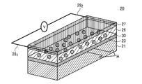
図16は、本発明の実施例2の光-スピン流変換素子の概念的斜視図であり、GGG基板21上に反強磁性体層であるIrMn層30をスパッタリング法で堆積したのち、上述の実施例1と同様に、Au含有Bi:YIG層26及びPt膜27を成膜し、Pt膜27の両端に電圧取り出し用の一対の電極281,282を設ける。
この実施例2の光-スピン流変換素子においては、磁場印加手段として、反強磁性体層であるIrMn層30を用い、その磁化方向を一対の電極281,282の対向方向と垂直方向に設定して磁場Hを印加する。
このように、本発明の実施例2においては、光-スピン流変換素子自体に磁場印加手段を設けているので、磁場印加手段を外部に設定する必要がなく、例えば、携帯機器に装着した場合に、環境中に光さえあれば簡単に電力を発生させることができる。
次に、図17を参照して、本発明の実施例3の光-スピン流変換素子を説明するが、この実施例3の光-スピン流変換素子は、表面プラズモン共鳴発生部材として光学プリズムを用いたものである。
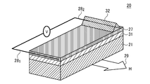
図17は、本発明の実施例3の光-スピン流変換素子の概念的斜視図であり、GGG基板21上にBi:YIG層31及びPt膜27を成膜し、Pt膜27の両端に電圧取り出し用の一対の電極281,282を設ける。次いで、Pt膜27の一端側に光学マイクロプリズム32を接着する。
照射光を光学マイクロプリズム32とPt膜27との界面で全反射が生ずる角度で入射させると、その時に発生するエバネッセント波により表面プラズモンを共鳴的に励起することができ、それによって、Pt膜27における電子有効温度を上昇させることができる。
その結果、Pt膜27における電子有効温度T*
e,PがBi:YIG層31におけるマグノン有効温度T*
m,Fより高くなるので、バックフロースピン流Jflの方がスピンポンピングスピン流Jspより大きくなり、その差分(Jfl-Jsp)がスピン流JsとしてPt層に誘起される。この時、一対の電極281,282の対向方向に磁場Hを印加しておくと、一つの電極281,282間に起電力EISHEが出力される。
次に、図18を参照して、本発明の実施例4の光-スピン流変換素子を説明するが、この実施例3の光-スピン流変換素子は、表面プラズモン共鳴発生部材として回折格子を用いたものである。
図18は、本発明の実施例4の光-スピン流変換素子の概念的斜視図であり、GGG基板21上にBi:YIG層31及びPt膜27を成膜する。次いで、Au膜を成膜し、レジストを塗布し、電子線リソグラフィー等で回折格子パターンを形成したのち、スパッターエッチングを行うことでAu膜の露出部をエッチングして回折格子33を形成する。もしくは、Au膜の成膜前にレジストを塗布し、電子線リソグラフィー等で回折格子パターンを形成したのちにAu膜を成膜し、リフトオフ法により回折格子33を形成しても良い。また、Pt膜27の両端に電圧取り出し用の一対の電極281,282を設ける。
照射光を回折格子33に照射すると、回折格子33によってブラッグ反射された回折波の分散直線がプラズモンの分散曲線と交差するようになるので、Pt膜27の表面に表面プラズモンを共鳴的に励起することができる。
その結果、Pt膜27における電子有効温度T*
e,PがBi:YIG層31におけるマグノン有効温度T*
m,Fより高くなるので、バックフロースピン流Jflの方がスピンポンピングスピン流Jspより大きくなり、その差分(Jfl-Jsp)がスピン流JsとしてPt層に誘起される。この時、一対の電極281,282の対向方向に磁場Hを印加しておくと、一つの電極281,282間に起電力EISHEが出力される。
次に、図19を参照して、本発明の実施例5の光-スピン流変換素子を説明するが、この実施例5の光-スピン流変換素子は、表面プラズモン共鳴発生部材として逆スピンホール効果部材層と一体になった回折格子を用いたものである。
図19は、本発明の実施例5の光-スピン流変換素子の概念的斜視図であり、GGG基板21上にBi:YIG層31を成膜したのち、厚めのAu膜を成膜する。次いで、レジストを塗布し、回折格子パターンを形成したのち、スパッターエッチングを行うことでAu膜の露出部の表面をエッチングして回折格子34とするとともに、下層のAu膜を逆スピンホール効果部材層35とする。
この実施例5の光-スピン流変換素子においても、起電力が得られるメカニズムは上記の実施例4と同様である。なお、この実施例5の場合も、回折格子の形成工程において、Au膜の成膜前にレジストを塗布し、電子線リソグラフィー等で回折格子パターンを形成したのちにAu膜を成膜し、リフトオフ法により回折格子33を形成しても良い。
10 光-スピン流変換素子
11 基板
12 磁性体層
13 逆スピンホール効果部材層
141~143 表面プラズモン共鳴発生部材
151,152 電極
16 磁場印加手段
20 光-スピン流変換素子
21 GGG基板
22 Au膜
23 Au微粒子
24 MOD溶液
25 酸化物層
26 Au含有Bi:YIG層
27 Pt膜
281,282:電極
29 磁場印加手段
30 IrMn層
31 Bi:YIG層
32 光学マイクロプリズム
33 回折格子
34 回折格子
35 逆スピンホール効果部材層
41 光ファイバ
42 デジタル光プロセッサ
43 光源
44 分光光学系
11 基板
12 磁性体層
13 逆スピンホール効果部材層
141~143 表面プラズモン共鳴発生部材
151,152 電極
16 磁場印加手段
20 光-スピン流変換素子
21 GGG基板
22 Au膜
23 Au微粒子
24 MOD溶液
25 酸化物層
26 Au含有Bi:YIG層
27 Pt膜
281,282:電極
29 磁場印加手段
30 IrMn層
31 Bi:YIG層
32 光学マイクロプリズム
33 回折格子
34 回折格子
35 逆スピンホール効果部材層
41 光ファイバ
42 デジタル光プロセッサ
43 光源
44 分光光学系
Claims (12)
- 磁性体層と、
前記磁性体層に接合する逆スピンホール効果部材層と、
照射光による表面プラズモン共鳴により前記磁性体層のマグノン有効温度或いは逆スピンホール効果部材層の電子有効温度の少なくとも一方を高める表面プラズモン共鳴発生部材と
を有する光-スピン流変換素子。 - 前記表面プラズモン共鳴発生部材が、前記磁性体層に含まれる微細金属であることを特徴とする請求項1に記載の光-スピン流変換素子。
- 前記微細金属が、金微粒子或いは銀微粒子である請求項2に記載の光-スピン流変換素子。
- 前記表面プラズモン共鳴発生部材が、前記逆スピンホール効果部材層の表面に設けられたプリズムである請求項1に記載の光-スピン流変換素子。
- 前記表面プラズモン共鳴発生部材が、前記逆スピンホール効果部材層の表面に設けられた回折格子である請求項1に記載の光-スピン流変換素子。
- 前記回折格子が、前記逆スピンホール効果部材層と同じ材料で一体に形成されている請求項5に記載の光-スピン流変換素子。
- 前記磁性体層の磁化方向を規制する磁場印加手段を有する請求項1に記載の光-スピン流変換素子。
- 前記逆スピンホール効果部材層が、逆スピンホール効果により電圧を取り出すための一対の電極を有している請求項7に記載の光-スピン流変換素子。
- 前記磁性体層が、Y3Fe5-xGaxO12(但し、0≦x<5)またはBiドープのY3Fe5-xGaxO12(但し、0≦x<5)からなる請求項1に記載の光-スピン流変換素子。
- 前記逆スピンホール効果部材層が、Pt、Au、Pd、Ag、Bi、f軌道或いは3d軌道を有する遷移金属を有する元素、若しくはそれらの合金のいずれかを有する元素のいずれか、或いは、前記各材料とCu、Al、或いは、Siの合金のいずれかである請求項1に記載の光-スピン流変換素子。
- 前記逆スピンホール効果部材層が、PtまたはBiドープCuである請求項10に記載の光-スピン流変換素子。
- 基板上に金属薄膜を堆積する工程と、
熱処理により前記金属膜を溶融して表面張力により微細金属を形成する工程と、
前記微細金属を含む基板上に磁性体部材を堆積して微細金属を含有する磁性体層を形成する工程と、
前記磁性体層上に逆スピンホール効果部材層を形成する工程と
を有することを特徴とする光-スピン流変換素子の製造方法。
Priority Applications (1)
| Application Number | Priority Date | Filing Date | Title |
|---|---|---|---|
| JP2014522583A JP6164658B2 (ja) | 2012-06-29 | 2013-06-21 | 光−スピン流変換素子及びその製造方法 |
Applications Claiming Priority (2)
| Application Number | Priority Date | Filing Date | Title |
|---|---|---|---|
| JP2012147846 | 2012-06-29 | ||
| JP2012-147846 | 2012-06-29 |
Publications (1)
| Publication Number | Publication Date |
|---|---|
| WO2014002881A1 true WO2014002881A1 (ja) | 2014-01-03 |
Family
ID=49783038
Family Applications (1)
| Application Number | Title | Priority Date | Filing Date |
|---|---|---|---|
| PCT/JP2013/067042 Ceased WO2014002881A1 (ja) | 2012-06-29 | 2013-06-21 | 光-スピン流変換素子及びその製造方法 |
Country Status (2)
| Country | Link |
|---|---|
| JP (1) | JP6164658B2 (ja) |
| WO (1) | WO2014002881A1 (ja) |
Cited By (5)
| Publication number | Priority date | Publication date | Assignee | Title |
|---|---|---|---|---|
| CN107192989A (zh) * | 2017-06-13 | 2017-09-22 | 电子科技大学 | 一种微波射频接收机 |
| CN110176533A (zh) * | 2019-05-10 | 2019-08-27 | 电子科技大学 | 一种光响应的自旋电子器件及其制备方法 |
| CN110579726A (zh) * | 2019-10-15 | 2019-12-17 | 哈尔滨理工大学 | 一种基于spr的高灵敏度磁场传感装置 |
| CN111511231A (zh) * | 2018-01-12 | 2020-08-07 | 菲利普莫里斯生产公司 | 包括等离子体加热元件的气溶胶生成装置 |
| WO2022239615A1 (ja) * | 2021-05-14 | 2022-11-17 | 国立大学法人東北大学 | 磁気メタマテリアル、スピン流制御装置及びスピン流制御方法 |
Citations (1)
| Publication number | Priority date | Publication date | Assignee | Title |
|---|---|---|---|---|
| WO2012169509A1 (ja) * | 2011-06-07 | 2012-12-13 | 日本電気株式会社 | 熱電変換素子 |
-
2013
- 2013-06-21 JP JP2014522583A patent/JP6164658B2/ja not_active Expired - Fee Related
- 2013-06-21 WO PCT/JP2013/067042 patent/WO2014002881A1/ja not_active Ceased
Patent Citations (1)
| Publication number | Priority date | Publication date | Assignee | Title |
|---|---|---|---|---|
| WO2012169509A1 (ja) * | 2011-06-07 | 2012-12-13 | 日本電気株式会社 | 熱電変換素子 |
Non-Patent Citations (2)
| Title |
|---|
| HARTLAND GV.: "Coherent excitation of vibrational modes in metallic nanoparticles", ANNUAL REVIEW PHYSICAL CHEMISTRY, vol. 57, 16 January 2006 (2006-01-16), pages 403 - 430 * |
| KEN-ICHI UCHIDA ET AL.: "Observation of longitudinal spin- Seebeck effect in magnetic insulators", APPLIED PHYSICS LETTERS, vol. 97, 29 October 2010 (2010-10-29), pages 172505 * |
Cited By (9)
| Publication number | Priority date | Publication date | Assignee | Title |
|---|---|---|---|---|
| CN107192989A (zh) * | 2017-06-13 | 2017-09-22 | 电子科技大学 | 一种微波射频接收机 |
| CN111511231A (zh) * | 2018-01-12 | 2020-08-07 | 菲利普莫里斯生产公司 | 包括等离子体加热元件的气溶胶生成装置 |
| US11896052B2 (en) | 2018-01-12 | 2024-02-13 | Philip Morris Products S.A. | Aerosol-generating device comprising a plasmonic heating element |
| CN110176533A (zh) * | 2019-05-10 | 2019-08-27 | 电子科技大学 | 一种光响应的自旋电子器件及其制备方法 |
| CN110579726A (zh) * | 2019-10-15 | 2019-12-17 | 哈尔滨理工大学 | 一种基于spr的高灵敏度磁场传感装置 |
| WO2022239615A1 (ja) * | 2021-05-14 | 2022-11-17 | 国立大学法人東北大学 | 磁気メタマテリアル、スピン流制御装置及びスピン流制御方法 |
| JPWO2022239615A1 (ja) * | 2021-05-14 | 2022-11-17 | ||
| US20240237552A1 (en) * | 2021-05-14 | 2024-07-11 | Tohoku University | Magnetic metamaterial, spin current control apparatus, and spin current control method |
| JP7565563B2 (ja) | 2021-05-14 | 2024-10-11 | 国立大学法人東北大学 | 磁気メタマテリアル、スピン流制御装置及びスピン流制御方法 |
Also Published As
| Publication number | Publication date |
|---|---|
| JP6164658B2 (ja) | 2017-07-19 |
| JPWO2014002881A1 (ja) | 2016-05-30 |
Similar Documents
| Publication | Publication Date | Title |
|---|---|---|
| JP5585314B2 (ja) | 熱電変換素子及び熱電変換装置 | |
| US8254163B2 (en) | Spintronic device and information transmitting method | |
| JP6143051B2 (ja) | スピントロニクスデバイス | |
| JP6164658B2 (ja) | 光−スピン流変換素子及びその製造方法 | |
| Liang et al. | Magnetotransport in Co-doped ZnO nanowires | |
| US9991436B2 (en) | Thermoelectric converter element, method of manufacturing thermoelectric converter element, and thermoelectric conversion method | |
| US20110084349A1 (en) | Thermoelectric conversion device | |
| Ren et al. | Electric field-induced magnetic switching in Mn: ZnO film | |
| CN108767107B (zh) | 一种电场调控的二维自旋电子器件及其制备方法 | |
| Li et al. | Thermoelectrical properties of silicon substrates with nanopores synthesized by metal-assisted chemical etching | |
| CN103718257B (zh) | 用于磁性物质元件的层叠体、包括该层叠体的热电转换元件及制造该层叠体的方法 | |
| US10326069B2 (en) | Thermoelectric conversion element and method for making the same | |
| Lezier et al. | Fully reversible magnetoelectric voltage controlled THz polarization rotation in magnetostrictive spintronic emitters on PMN-PT | |
| US9647193B2 (en) | Thermoelectric conversion element and thermoelectric conversion device | |
| WO2012169509A1 (ja) | 熱電変換素子 | |
| JPWO2017082266A1 (ja) | 熱電変換素子用起電膜及び熱電変換素子 | |
| Chang et al. | Tuning electronic transport in a self-assembled nanocomposite | |
| Matsuo et al. | Anomalous Hall effect in nanoscale structures of the antiferromagnetic Weyl semimetal Mn3Sn at room temperature | |
| WO2012121230A1 (ja) | 音波-スピン流変換素子 | |
| KR20240044257A (ko) | 스핀-전하 변환 제어 소자 및 이의 제조 방법 | |
| JP7505310B2 (ja) | 熱電変換材料 | |
| JP6349863B2 (ja) | スピン流熱電変換素子とその製造方法および熱電変換装置 | |
| WO2014041838A1 (ja) | 熱電変換素子及びその製造方法 | |
| CN210866183U (zh) | 一种电可控的二维自旋电子器件阵列 | |
| Wang et al. | Analysis of the magnetic and optical properties of (Fe, V)-co-doped 3C–SiC using first-principles calculations |
Legal Events
| Date | Code | Title | Description |
|---|---|---|---|
| 121 | Ep: the epo has been informed by wipo that ep was designated in this application |
Ref document number: 13809846 Country of ref document: EP Kind code of ref document: A1 |
|
| ENP | Entry into the national phase |
Ref document number: 2014522583 Country of ref document: JP Kind code of ref document: A |
|
| NENP | Non-entry into the national phase |
Ref country code: DE |
|
| 122 | Ep: pct application non-entry in european phase |
Ref document number: 13809846 Country of ref document: EP Kind code of ref document: A1 |