WO2014002371A1 - タッチパネルコントローラ、タッチパネルシステムおよび電子機器 - Google Patents
タッチパネルコントローラ、タッチパネルシステムおよび電子機器 Download PDFInfo
- Publication number
- WO2014002371A1 WO2014002371A1 PCT/JP2013/003236 JP2013003236W WO2014002371A1 WO 2014002371 A1 WO2014002371 A1 WO 2014002371A1 JP 2013003236 W JP2013003236 W JP 2013003236W WO 2014002371 A1 WO2014002371 A1 WO 2014002371A1
- Authority
- WO
- WIPO (PCT)
- Prior art keywords
- touch panel
- amplifier
- switch
- switch means
- drive
- Prior art date
- Legal status (The legal status is an assumption and is not a legal conclusion. Google has not performed a legal analysis and makes no representation as to the accuracy of the status listed.)
- Ceased
Links
Images




Classifications
-
- G—PHYSICS
- G06—COMPUTING OR CALCULATING; COUNTING
- G06F—ELECTRIC DIGITAL DATA PROCESSING
- G06F3/00—Input arrangements for transferring data to be processed into a form capable of being handled by the computer; Output arrangements for transferring data from processing unit to output unit, e.g. interface arrangements
- G06F3/01—Input arrangements or combined input and output arrangements for interaction between user and computer
- G06F3/03—Arrangements for converting the position or the displacement of a member into a coded form
- G06F3/041—Digitisers, e.g. for touch screens or touch pads, characterised by the transducing means
- G06F3/0412—Digitisers structurally integrated in a display
-
- G—PHYSICS
- G06—COMPUTING OR CALCULATING; COUNTING
- G06F—ELECTRIC DIGITAL DATA PROCESSING
- G06F3/00—Input arrangements for transferring data to be processed into a form capable of being handled by the computer; Output arrangements for transferring data from processing unit to output unit, e.g. interface arrangements
- G06F3/01—Input arrangements or combined input and output arrangements for interaction between user and computer
- G06F3/03—Arrangements for converting the position or the displacement of a member into a coded form
- G06F3/041—Digitisers, e.g. for touch screens or touch pads, characterised by the transducing means
- G06F3/0416—Control or interface arrangements specially adapted for digitisers
- G06F3/0418—Control or interface arrangements specially adapted for digitisers for error correction or compensation, e.g. based on parallax, calibration or alignment
-
- G—PHYSICS
- G06—COMPUTING OR CALCULATING; COUNTING
- G06F—ELECTRIC DIGITAL DATA PROCESSING
- G06F3/00—Input arrangements for transferring data to be processed into a form capable of being handled by the computer; Output arrangements for transferring data from processing unit to output unit, e.g. interface arrangements
- G06F3/01—Input arrangements or combined input and output arrangements for interaction between user and computer
- G06F3/03—Arrangements for converting the position or the displacement of a member into a coded form
- G06F3/041—Digitisers, e.g. for touch screens or touch pads, characterised by the transducing means
- G06F3/044—Digitisers, e.g. for touch screens or touch pads, characterised by the transducing means by capacitive means
- G06F3/0446—Digitisers, e.g. for touch screens or touch pads, characterised by the transducing means by capacitive means using a grid-like structure of electrodes in at least two directions, e.g. using row and column electrodes
Definitions
- the present invention relates to a touch panel controller, a touch sensor panel, and a touch panel controller that detect a touch position on a screen by driving a drive line of a touch sensor panel to estimate or detect a capacitance value of a capacitance between the sense line and the drive line.
- the present invention relates to a touch panel system using a touch panel and an electronic device using the touch panel system.
- a touch sensor panel mounted on a display screen of a display device is known as a conventional position input device that detects a position where capacitance values distributed in a matrix are changed.
- a conventional capacitance detection device that detects a distribution of capacitance values of a capacitance matrix formed between M drive lines and L sense lines orthogonal thereto is disclosed as a touch sensor panel. It is proposed in Document 1.
- the touch sensor panel as the conventional capacitance detection device touches the touch panel surface with a finger or a pen
- the capacitance value at the touched position changes. This is detected as an input position touched by the pen.
- FIG. 9 is a schematic diagram showing a configuration example of a main part of a conventional touch panel system disclosed in Patent Document 1.
- FIG. 10 is a diagram for explaining an example of a driving method of the touch panel system of FIG.
- capacity detection is performed by driving a plurality of drive lines in parallel (simultaneously), but here, a simple example is shown to explain the basic principle of capacity detection.
- the conventional touch panel system 100 drives the touch sensor panel 110, the touch panel controller 120 that detects the position where the capacitance of the touch sensor panel 110 has changed, and the drive lines DL1 to DL4 of the touch sensor panel 110. And a drive unit 130.
- the touch sensor panel 110 includes a plurality of drive lines DL1 to DL4 arranged in the vertical direction, a plurality of sense lines SL1 to SL4 that are three-dimensionally intersected with the drive lines DL1 to DL4, and a plurality of drive lines DL1.
- the description is simplified when the number of drive lines DL1 to DL4 and the number of sense lines SL1 to SL4 are 4 ⁇ 4.
- the touch panel system 100 is provided with a drive unit 130.
- the drive unit 130 drives the drive lines DL1 to DL4 based on the 4 ⁇ 4 code sequence shown in (Equation 3) of FIG. If the element of the code matrix is “1”, the drive unit 130 applies the voltage Vdrive, and if the element is “0”, it applies zero volts. In short, the driving unit 130 sequentially drives the drive lines DL1 to DL4.
- the touch panel system 100 has four amplifiers 140 arranged at positions corresponding to the sense lines SL1 to SL4, respectively.
- the amplifier 140 receives and amplifies the linear sums Y1, Y2, Y3, and Y4 of the electrostatic capacitances along the sense line through the drive line driven by the driving unit 130.
- the drive unit 130 applies the voltage Vdrive to the drive line DL1, and applies zero volts to the remaining drive lines DL2 to DL4. Then, for example, the measured value Y1 from the sense line SL3 corresponding to the capacitance C31 shown in (Equation 1) of FIG.
- the voltage Vdrive is applied to the drive line DL2, and zero volts is applied to the remaining drive lines DL1, DL3, and DL4. Then, the measured value Y2 from the sense line SL3 corresponding to the capacitance C32 shown in (Equation 2) of FIG.
- the voltage Vdrive is applied to the drive line DL3, and zero volts is applied to the remaining drive lines.
- the voltage Vdrive is applied to the drive line DL4, and zero volts is applied to the remaining drive lines.
- the above is a basic configuration example of the conventional touch panel system 100 including the touch sensor panel 110, the touch panel controller 120, and the driving unit 130.
- Patent Document 2 proposes a touch panel system as a capacity detection device having another configuration.
- FIG. 11 is a configuration diagram showing a configuration example of a conventional touch panel controller disclosed in Patent Document 2.
- the conventional touch panel controller 200 there is a differential amplifier 201 for detecting the position capacitance of the touch sensor panel, and a switch SW1 that can switch the connection state of the input section of the differential amplifier 201, SW2, SW3 and SW4 and a selection circuit are arranged. Switching between the differential input mode and the single input mode is realized by the states of the switches SW1, SW2, SW3, and SW4.
- it is configured to detect the capacitance or capacitance difference of the input line selected by the selection circuit and estimate the location of capacitance change due to touch.
- Vref / 2 generated by the reference voltage source 202 is different from the operating point voltage of the differential amplifier 201 even when the SW4 is turned off, an error due to a leakage current is generated only in one input of the differential amplifier 201. Therefore, there is a problem that an error is mixed in the output value from the differential amplifier 201.
- the present invention solves the above-mentioned conventional problem, and reduces the influence of error factors due to leakage current via an off-resistance when a switch is arranged on the input side of an amplifier, and more accurate capacitance change It is an object of the present invention to provide a touch panel controller that can correctly detect a touch panel, a good touch panel system using the touch panel controller, and a good electronic device using the touch panel controller.
- the touch panel controller of the present invention drives a plurality of drive lines of a touch sensor panel, amplifies the capacitance value of the capacitance between the sense line and the drive line by an amplifier, and then estimates or detects the capacitance value on the screen.
- the touch panel controller for detecting a touch position, at least two switch means connected in series between the input terminal of the amplifier and the sense line, and when the two switch means are in an OFF state, And a predetermined voltage applying means for applying a predetermined voltage to a node between them, thereby achieving the above object.
- the predetermined voltage applying means in the touch panel controller of the present invention comprises: a switch means having one end connected to the node; and a predetermined voltage output unit connected to the other end of the switch means and outputting a predetermined voltage.
- a switch means having one end connected to the node
- a predetermined voltage output unit connected to the other end of the switch means and outputting a predetermined voltage.
- the predetermined voltage in the touch panel controller of the present invention is the same voltage as the operating point voltage of the amplifier or a voltage of Vdd / 2.
- At least two switch means connected in series in the touch panel controller of the present invention are CMOS switch means or MEMS switch means.
- At least one drive line in the touch panel controller of the present invention is sequentially driven one by one, and a plurality of first static lines formed between the plurality of drive lines and each one of the sense lines.
- a drive unit that outputs a first linear sum output from the capacitance from each one sense line, and the amplifier amplifies the first linear sum output with one input.
- the plurality of drive lines in the touch panel controller of the present invention are sequentially driven at least one by one and formed between the plurality of drive lines and one of the plurality of sense lines.
- a first linear sum output from the plurality of first capacitances is output from the one sense line, and the plurality of drive lines and another one sense line adjacent to the one sense line;
- a driving unit for outputting a second linear sum output from a plurality of second capacitances formed between the other one of the sense lines, and the amplifier includes the first linear sum output and the first linear sum output.
- This is a differential amplifier that differentially amplifies the difference between the two linear sum outputs.
- a plurality of switch means for exchanging the drive line and the sense line with each other are provided between the amplifier and the drive line and the sense line corresponding thereto in the touch panel controller of the present invention
- Each of the plurality of switch means includes at least two switch means connected in series and a predetermined voltage applying means for applying a predetermined voltage to a node between the two switch means when the two switch means are in an OFF state. And have.
- the capacitance values of the capacitances in the plurality of sense lines in the touch panel controller of the present invention are each amplified in a time division manner using one amplifier.
- the touch panel controller in the touch panel controller according to the present invention, at least two switch means connected in series between one input terminal of the one amplifier and the plurality of sense lines, and the two switches And a predetermined voltage applying means for applying a predetermined voltage to a node between the two switch means when the means is in an OFF state.
- the touch panel controller of the present invention at least two switch means connected in series between one input terminal of the one amplifier and the plurality of sense lines, and the two switches And a predetermined voltage applying means for applying a predetermined voltage to a node between the two switch means when the means is in an OFF state, and each between the other input terminal of the one amplifier and the plurality of sense lines. And at least two switch means connected in series, and the predetermined voltage applying means for applying a predetermined voltage to a node between the two switch means when the two switch means are in an OFF state.
- the configuration connected to both differential input terminals of the differential amplifier in the touch panel controller of the present invention is a symmetrical circuit configuration.
- the touch panel system of the present invention includes the touch panel controller of the present invention and the touch sensor panel used for the touch panel controller, thereby achieving the above object.
- the electronic device of the present invention uses the touch panel system of the present invention as a position input device on a display screen, thereby achieving the above object.
- the capacitance value is estimated or detected to determine the touch position on the screen.
- the touch panel controller to detect, at least two switch means connected in series between the input terminal of the amplifier and the sense line, and a node between the two switch means when the two switch means are in an OFF state And a predetermined voltage applying means for applying a predetermined voltage.
- FIG. 2 is a circuit diagram showing a detailed configuration of each of switches SW1 to SW4 used in the touch panel system of FIG.
- FIG. 1 it is a schematic diagram for demonstrating the case where it amplifies sequentially by a time division using one amplifier with respect to several sense line SL.
- FIG. 5 is a schematic diagram for explaining a case where a plurality of sense lines SL are sequentially amplified in a time-division manner using a single 2-input differential amplifier in the touch panel system of FIG. 4.
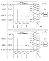
- FIG. 6 is a schematic diagram showing a case where the touch panel system 1Aa of FIG. 5 is connected as a chip A and a chip B.
- FIG. It is a block diagram which shows schematic structural example of electronic devices, such as a mobile telephone apparatus using the touchscreen system of Embodiment 1, 2 of this invention as Embodiment 3 of this invention. It is a schematic diagram which shows the principal part structural example of the conventional touch panel system currently disclosed by patent document 1.
- FIG. It is a figure for demonstrating an example of the drive method of the touchscreen system of FIG.
- FIG. 2 shows the structural example of the conventional touchscreen controller currently disclosed by patent document 2.
- Embodiments 1 and 2 of the touch panel controller of the present invention and a touch panel system using the same, and Embodiment 3 of an electronic apparatus such as a camera-equipped mobile phone using the same will be described in detail with reference to the drawings. explain.
- FIG. 1 is a schematic diagram illustrating a configuration example of a main part of a touch panel system according to Embodiment 1 of the present invention.
- the touch panel system 1 is generated between a touch sensor panel 10, M drive lines DL1 to DLm of the touch sensor panel 10, and N sense lines SL1 to SLn that are three-dimensionally intersected therewith. And a touch panel controller 20 that detects positions where a plurality of matrix capacitances C11 to Cnm change.
- the touch sensor panel 10 includes M drive lines DL1 to DLm arranged in the vertical direction, and three sense lines SL1 to SLn arranged in the horizontal direction and M drive lines DL1 to DLm arranged in the horizontal direction. A plurality of holding portions of capacitances C11 to Cnm are generated at the positions where the lines DL1 to DLm and the N sense lines SL1 to SLn intersect.
- the touch sensor panel 10 is arranged on the display screen of the display unit, and the touch panel controller 20 detects a touch position on the touch sensor panel 10 with a finger or a pen.
- the touch panel controller 20 includes a driving unit 2 that sequentially drives at least one of the M drive lines DL1 to DLm of the touch sensor panel 10, an amplifier 3 that amplifies a capacitance signal from the sense lines SL1 to SLn, and a driving unit 2 And switch means 4 for exchanging the drive lines DL1 to DLm and the sense lines SL1 to SLn between the drive lines DL1 to DLm and the sense lines SL1 to SLn.
- the touch panel controller 20 detects a position on the touch sensor panel 10 where the capacitance has changed, using the amplified output from the amplifier 3 constituting the previous stage.
- the driving unit 2 sequentially drives at least one drive line DL1 to DLm sequentially based on the code sequence of n rows and m columns. If the element of the code matrix is “1”, the driving unit 2 applies a drive voltage, and if the element of the code matrix is “0”, it applies zero volts.
- the elements of the code matrix are not limited to binary, but may be multivalued. For example, if the element of the code matrix is “ ⁇ 1”, a minus drive voltage is applied, and if the element of the code matrix is “0.5”, a voltage that is half the drive voltage of “1” is applied. .
- the drive unit 2 sequentially drives at least one of the drive lines DL1 to DLm based on a code sequence having a length P (P ⁇ M), and a plurality of first capacitances Ca1 to Cam (a is A first linear sum output from a natural number (a ⁇ n) is output from one sense line SLa (a is an arbitrary number of sense lines SL).
- the amplifier 3 includes a plurality of drive lines DL1 to DLm that are sequentially driven and a plurality of N sense lines SL1 to SLn that intersect with the drive lines DL1 to DLm.
- the first linear sum output from the first capacitances C11 to Cnm is amplified and output with one input.
- the amplifier 3 is arranged for each of the N sense lines SL1 to SLn.
- the N sense lines SL1 to SLn may be configured to be amplified and output in a time division manner using a single amplifier 3a described later. This case is shown in FIG.
- the switch means 4 includes switches SW1 to SW4, and can switch the drive lines DL1 to DLm and the sense lines SL1 to SLn by on / off control of the switches SW1 to SW4.
- the drive voltage supply end of the drive line DLm is connected to the amplifier input end which is the end of the sense line SLn via the switch SW1.
- the drive voltage supply end of the drive line DLm is connected to the inverter output end of the drive unit 2 via the switch SW2.
- An end portion of the sense line SLn is connected to a connection point between the amplifier input end and the switch SW1 via the switch SW3.
- the connection point between the switch SW2 and the inverter output terminal of the drive unit 2 is connected to the connection point between the end of the sense line SLn and the switch SW3 via the switch SW4.
- the drive line DL and the sense line SL work normally, but when this function is switched, the switch SW2 and the switch SW3 are off. Thus, the switch SW1 and the switch SW4 are turned on.
- the drive voltage supply terminal of the drive line DL is connected to the amplifier input terminal via the switch SW1, and the drive line is no longer a sense line.
- the inverter output terminal of the drive unit 2 is connected to the end of the sense line SLn via the switch SW4 to drive the sense line SL, and the sense line is no longer a drive line.
- the switch SW1 is turned off to open the connection between the end portion of the drive line DL and the amplifier input end, and the end portion of the sense line SL is connected to the amplifier input end via the switch SW3.
- the switch SW4 is turned off to open the connection between the inverter output terminal of the drive unit 2 and the end of the sense line SL, and the inverter output terminal of the drive unit 2 is connected to the drive voltage drive terminal of the drive line via the switch SW2. Connect to.
- the switch SW3 When the drive line DL is switched to the sense line SL, the switch SW3 is turned off to open the connection between the end of the sense line SL and the amplifier input end, and the drive line drive voltage supply end is input to the amplifier via the switch SW1. Connect to the end.
- the switch SW2 When the sense line SL is switched to the drive line DL, the switch SW2 is turned off to open the connection between the inverter output terminal of the drive unit 2 and the drive voltage supply terminal of the drive line, and the inverter output terminal of the drive unit 2 is The switch SW4 is connected to the end of the sense line SL.
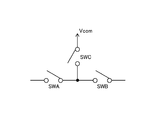
- FIG. 2 is a circuit diagram showing a detailed configuration of each of the switches SW1 to SW4 used in the touch panel system 1 of FIG.
- each of the switches SW1 to SW4 of the line replacement mechanism has a T-shaped connection configuration in which one end of the switch SWC is connected to a connection point between the two switches SWA and SWB.
- Two switches SWA and SWB turn the line on or off.
- a predetermined voltage is applied to the connection point thereof via the switch SWC.
- This predetermined voltage is the same voltage as the operating point voltage of the amplifier 2 (for example, Vdd / 2).
- Switches SW1 to SW4 are provided as switch means 4 between the input terminal of the amplifier 3 and the drive line DL and sense line SL.
- Each switch SW constituting the switch means 4 includes at least two switches SWA and SWB connected in series, and two switches SWA and SWB when the at least two switches SWA and SWB are in an OFF state.
- a predetermined voltage applying means for applying a predetermined voltage via the switch SWC.
- the predetermined voltage applying means includes a switch SWC and a predetermined voltage output unit Vcom that outputs a predetermined voltage to the node via the switch SWC.
- the same voltage for example, Vdd / 2
- Vdd / 2 the same voltage
- the amplifier side voltages of the two switches SWA and SWB and the connection point voltage of the two switches SWA and SWB are the same voltage, and no leakage current flows through the switch-off resistor. Therefore, it is possible to eliminate or reduce the influence of the error factor due to the leakage current through the off-resistance when the switch is arranged on the input side of the amplifier 2, and to detect the capacitance change of the capacitance more accurately and quickly. it can.
- the present invention is not limited to this, and one amplifier 3a described later is used for the plurality of sense lines SL. You may make it amplify sequentially by a time division. This case is shown in FIG.
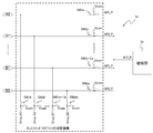
- FIG. 3 is a schematic diagram for explaining a case where the touch panel system 1 in FIG. 1 sequentially amplifies a plurality of sense lines SL in a time division manner using one amplifier.
- the sense line SL and the drive line DL are shown in common for the sense line / drive line switching mechanism.
- a switch SW1a, a switch SW2a,..., A switch SW (n-1) a, and a switch SWna are sequentially turned on from the OFF state at the input terminal of one amplifier 3a.
- a switch SW (n-1) a, and a switch SWna are sequentially turned on from the OFF state at the input terminal of one amplifier 3a.
- N switches SW for switching each sense line SL are required instead. And the processing speed is slow.
- the line switching mechanism (sense line / drive line switching mechanism) of the plurality of drive lines DL and the plurality of sense lines SL is the switches SW1b to SWmb of the switching mechanism of the drive lines DL and the senses.
- the switches SL1a to SWna of the line SL switching mechanism are provided.
- the switch means in which one end of the switch SWC is connected to the connection point between the two switches SWA and SWB is used for each of the switches SW1a to SWna and SW1b to SWmb. Also in this case, when the two switches SWA and SWB are turned off, a predetermined voltage is applied to the connection point via the switch SWC to suppress or prevent the switch-off current.
- This predetermined voltage is preferably the same voltage as the operating point voltage of the amplifier 2 (for example, Vdd / 2). As a result, the leakage current from other lines can be suppressed.
- the switches SW1b to SWmb constituting the line replacement mechanism and the switches SW1a to SWna for switching the sense lines SL for one amplifier 3a are respectively provided with two switches SWA. And a switch means in which one end of the switch SWC is connected to the connection point of the switch SWB, and when the two switches SWA and SWB are turned off, a switch means for applying a predetermined voltage to the connection point via the switch SWC is applied.
- the present invention is not limited to this, and in the case where there is no line replacement mechanism, two switches SWA and SWB are connected to the switches SW1a to SWna for switching each sense line SL for one amplifier 3a.
- One end of the switch SWC is connected to the point When the two switches SWA and SWB are turned off, a predetermined voltage (for example, the same voltage as the operating point voltage of the amplifier 2; for example, Vdd / 2) is applied to the connection point between the switches SWA and SWB via the switch SWC. Only the switch means may be applied.
- a predetermined voltage for example, the same voltage as the operating point voltage of the amplifier 2; for example, Vdd / 2
- the touch panel controller 20 for detecting the touch position on the screen by estimating or detecting the capacitance value after amplification by the amplifier 3, at least two switch means connected in series between the input terminal of the amplifier 3 and the sense line SL SWA, SWB, and a predetermined voltage application unit Vcom for outputting a predetermined voltage via the switch means SWC to a node between the two switch means SWA, SWB when the two switch means SWA, SWB are in an OFF state. ing.
- a plurality of drive lines DL are sequentially driven one by one, and a first linear sum output from a plurality of first capacitances formed between the plurality of drive lines DL and each one sense line SL is generated.
- the drive unit 2 outputs the signal from one sense line SL.
- the amplifier 3 amplifies the first linear sum output with one input.
- SWB has predetermined voltage application means (here, switch SWC and voltage source Vcom) for applying a predetermined voltage to the node between SWB, so that switch means (switches SW1, SW3) are arranged on the input side of the amplifier 3 or 3a.
- predetermined voltage application means here, switch SWC and voltage source Vcom
- the leakage current from other lines can be suppressed, the sense line and the drive line can be shared, and the versatility of the chip can be improved.
- FIG. 4 is a schematic diagram illustrating a configuration example of a main part of the touch panel system according to the second embodiment of the present invention.
- the touch panel system 1A is generated between the touch sensor panel 10A, M drive lines DL1 to DLm of the touch sensor panel 10A, and N sense lines SL1 to SLn that are three-dimensionally intersected with this. And a touch panel controller 20A that detects positions where a plurality of matrix capacitances C11 to Cnm change.
- the touch sensor panel 10A includes M drive lines DL1 to DLm arranged in the vertical direction and three sense lines SL1 to SLn arranged in the horizontal direction and M drive lines DL1 to DLm arranged in the horizontal direction. A plurality of holding portions of capacitances C11 to Cnm are generated at the positions where the lines DL1 to DLm and the N sense lines SL1 to SLn intersect.
- the touch sensor panel 10A is disposed on the display screen of the display unit, and the touch panel controller 20A detects a touch position on the touch sensor panel 10A with a finger or a pen.
- the touch panel controller 20A includes a drive unit 2A that sequentially drives at least one of the M drive lines DL1 to DLm of the touch sensor panel 10A, and an amplifier 3A that differentially amplifies two capacitance signals from the sense lines SL1 to SLn.
- the drive unit 2A and the drive lines DL1 to DLm and the sense lines SL1 to SLn have switch means 4A for exchanging the drive lines DL1 to DLm and the sense lines SL1 to SLn.
- the driving unit 2A sequentially drives at least one drive line DL1 to DLm sequentially based on the code sequence of n rows and m columns. If the element of the code matrix is “1”, the driving unit 2 applies a drive voltage, and if the element of the code matrix is “0”, it applies zero volts.
- the elements of the code matrix are not limited to binary, but may be multivalued. For example, if the element of the code matrix is “ ⁇ 1”, a minus drive voltage is applied, and if the element of the code matrix is “0.5”, a voltage that is half the drive voltage of “1” is applied. .
- the drive unit 2 sequentially drives at least one of the drive lines DL1 to DLm based on a code sequence having a length P (P ⁇ M), and thereby a plurality of first capacitance units Ca1 to Cam (a Is a natural number; a first linear sum output from a ⁇ n) is output from the two sense lines SLa.
- the amplifier 3A includes a plurality of drive lines DL1 to DLm that are sequentially driven and one of, for example, one of the N sense lines SL1 to SLn that intersect with the drive lines DL1 to DLm. Formed between the first linear sum output from the first capacitances C11 to C1m and the M drive lines DL1 to DLm and another sense line SL2 adjacent to the one sense line SL1. The difference component from the second linear sum output from the plurality of second capacitance units C21 to C2m is amplified and output.
- the amplifier 3A is arranged for each of N sense lines SL1 to SLn.
- the N sense lines SL1 to SLn may be configured to be differentially amplified and output in a time division manner using one amplifier 3A. This case is shown in FIG.
- the switch means 4A is composed of switches SW1 to SW4, and can switch the drive lines DL1 to DLm and the sense lines SL1 to SLn by on / off control of the switches SW1 to SW4.
- the drive voltage supply end of the drive line DLm-1 is connected to the amplifier input end which is the end of the sense line SLn-1 via the switch SW1.
- the drive voltage supply terminal of the drive line DLm-1 is connected to the inverter output terminal of the drive unit 2A via the switch SW2.
- the end of the sense line SLn-1 is connected to the connection point between the first amplifier input terminal and the switch SW1 via the switch SW3.
- the connection point between the switch SW2 and the inverter output terminal of the drive unit 2A is connected to the connection point between the end of the sense line SLn-1 and the switch SW3 via the switch SW4.
- the drive voltage supply terminal of the drive line DLm is connected to the amplifier input terminal which is the end of the sense line SLn via the switch SW1.
- the drive voltage supply end of the drive line DLm is connected to the inverter output end of the drive unit 2A via the switch SW2.
- An end portion of the sense line SLn is connected to a connection point between the amplifier input end and the switch SW1 via the switch SW3.
- the connection point between the switch SW2 and the inverter output end of the drive unit 2A is connected to the connection point between the end of the sense line SLn and the switch SW3 via the switch SW4.
- the drive line DL and the sense line SL work normally, but when this function is switched, the switch SW2 and the switch SW3 are off. Thus, the switch SW1 and the switch SW4 are turned on.
- the drive voltage supply terminal of the drive line DL is connected to the amplifier input terminal via the switch SW1, and the drive line is no longer a sense line.
- the inverter output terminal of the drive unit 2A is connected to the end of the sense line SLn via the switch SW4 to drive the sense line SL, and the sense line is no longer a drive line.
- the switch SW1 is turned off to open the connection between the end portion of the drive line DL and the amplifier input end, and the end portion of the sense line SL is connected to the amplifier input end via the switch SW3. Further, the switch SW4 is turned off to open the connection between the inverter output end of the drive unit 2A and the end of the sense line SL, and the inverter output end of the drive unit 2A is supplied to the drive line DL via the switch SW2. Connect to the end.
- the switch SW3 When the drive line DL is the sense line SL, the switch SW3 is turned off to open the connection between the end of the sense line SL and the amplifier input end, and the drive voltage supply end of the drive line DL is amplified via the switch SW1. Connect to the input end.
- the switch SW2 When the sense line SL is the drive line DL, the switch SW2 is turned off to open the connection between the inverter output terminal of the drive unit 2 and the drive voltage supply terminal of the drive line DL, and the inverter output terminal of the drive unit 2 Is connected to the end of the sense line SL via the switch SW4.
- each of the switches SW1 to SW4 has a T connection configuration in which one end of the switch SWC is connected to a connection point between the two switches SWA and SWB.
- a predetermined voltage is applied to the connection point thereof via the switch SWC.
- the predetermined voltage is the same voltage as the operating point voltage of the amplifier 2 (for example, Vdd / 2).
- a single two-input amplifier 3Aa may be used to sequentially amplify in a time division manner. This case is shown in FIG.
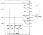
- FIG. 5 is a schematic diagram for explaining a case where the touch panel system 1A of FIG. 4 sequentially amplifies the plurality of sense lines SL by time division using one 2-input differential amplifier.
- the sense line SL and the drive line DL are shown in common for the sense line / drive line switching mechanism.
- the switch SW (n-2) a, the switch SW (n-1) a are sequentially turned off from the two input ends of one amplifier 3Aa.
- the switch SW (n ⁇ 1) a ′, the switch SWna ′ are sequentially turned off while the sense signal from each sense line SL is sequentially input to one input terminal. And the sense signal from each sense line SL is sequentially input to the other input terminal.
- Switch SW (n ⁇ 2) a and switch SW (n ⁇ 1) a ′, switch SW (n ⁇ 1) a and switch SWna ′ are sequentially input.
- N switches SW for switching the sense lines SL are required instead.
- the processing speed is slow.
- the line switching mechanism (sense line / drive line switching mechanism) between the plurality of drive lines DL and the sense line SL is the switch SW1b to the switch SWmb of the drive line DL switching mechanism and the switching of the sense line SL.
- the switches SW1a to SWna and SW1a ′ to SWna ′ of the mechanism are included.
- the switches SW1a to SWna and SW1a ′ to SWna ′, and further the switches SW1b to SWmb are constituted by switch means in which one end of the switch SWC is connected to the connection point of the two switches SWA and SWB. . Also in this case, when the two switches SWA and SWB are turned off, a predetermined voltage is applied to the connection point thereof via the switch SWC. This predetermined voltage is the same voltage as the operating point voltage of the amplifier 2 (for example, Vdd / 2). As a result, the leakage current from other lines can be suppressed.
- switches SW1b to SWmb constituting a line replacement mechanism (sense line / drive line switching mechanism) and switches for switching each sense line SL for one amplifier 3Aa.
- SW1a to switch SWna and switch SW1a ′ to switch SWna ′ are switch means in which one end of the switch SWC is connected to the connection point of the two switches SWA and SWB, respectively, and when the two switches SWA and SWB are turned off, Although switch means for applying a predetermined voltage via the switch SWC is applied to those connection points, the present invention is not limited to this, and there is no line replacement mechanism, and each sense line SL is connected to one amplifier 3Aa.
- Switch SW1a to switch Switch means in which one end of the switch SWC is connected to the connection point of the two switches SWA and SWB to each of Wna and the switch SW1a ′ to the switch SWna ′, and the connection is made when the two switches SWA and SWB are turned off.
- the switch means for applying a predetermined voltage for example, the same voltage as the operating point voltage of the amplifier 2; for example, Vdd / 2 to the point via the switch SWC may be applied.
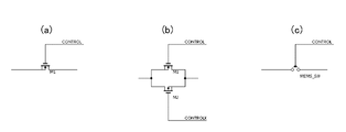
- the switches SWA, SWB, and SWC are the MOS transistor switch means of FIG. 6A, the CMOS switch means of FIG. 6B, and FIG. 6C. Any of these MEMS switch means may be combined.
- the CMOS switch means in the case of a switch composed only of NMOS or PMOS, the on-resistance increases at the time of high voltage or low voltage, so the CMOS switch means is required to realize a good on-resistance in a wide voltage range. desirable. Further, by using the MEMS switch means, the on-resistance of the switch is smaller and the off-resistance is larger, and a more ideal switching operation can be performed.
- FIG. 7 is a schematic diagram showing a case where the touch panel system 1Aa of FIG.
- a (N + 0) processed by chip A is also input to chip B.
- a (N + 2) and A (N + 1) processed by the chip B are affected via the off-resistance (switches SW1a and SW1a ').
- it is connected to the common voltage Vcom through an off-resistance.
- the (N + 0) line capacitance signal of the chip A is suppressed or prevented from being input to the chip B via the off-resistance (switches SW1a and SW1a ').
- the line of A (N + 0) processed by the chip A does not affect A (N + 2) and A (N + 1).
- the leakage current from other lines can be suppressed.
- the touch panel controller 20A for detecting the touch position on the screen by estimating or detecting the capacitance value after amplification by the amplifier 3A at least two connected in series between the two input terminals of the amplifier 3A and each sense line SL.
- the switch means SWA, SWB, and a predetermined voltage application unit Vcom that outputs a predetermined voltage via the switch means SWC to a node between the two switch means SWA, SWB when the two switch means SWA, SWB are in an OFF state.
- At least one of the plurality of drive lines DL is sequentially driven, and a plurality of first lines formed between the plurality of drive lines DL and one sense line SL among the plurality of sense lines SL intersecting therewith.
- the first linear sum output from the capacitance is output from one sense line SL, and between the plurality of drive lines DL and another sense line SL adjacent to the one sense line SL.
- a drive unit 2A for outputting a second linear sum output from a plurality of second capacitances to be formed from another sense line SL.
- the amplifier 3A has a first linear sum output and a second linear sum output.
- the differential amplifier differentially amplifies the difference between
- switch SWA and SWB connected in series between the two input terminals of the amplifier 3A or 3Aa and each sense line SL, and two when the two switches SWA and SWB are in the OFF state, respectively. Since it has predetermined voltage application means (here, switch SWC and voltage source Vcom) for applying a predetermined voltage to a node between the switches SWA and SWB, switch means (switches SW1 and SW3) are provided on the input side of the amplifier 3A or 3Aa. It is possible to reduce the influence of an error factor due to a leakage current via an off-resistance when it is arranged, and to accurately detect a capacitance change of capacitance more accurately.
- predetermined voltage application means here, switch SWC and voltage source Vcom
- leakage current from other lines can be suppressed. In this way, leakage current from other lines can be suppressed, the sense line and the drive line can be shared, and the versatility of the chip can be improved.
- the number of the M lines is different from that of the N lines, and the M lines are different.
- the number of amplifiers 3 or 3A or the number of wirings at the input end of the amplifier 3a or 3Aa is prepared in advance for M lines, or N is more than M If the number is too large, it is necessary to prepare the number of output terminals from the drive unit 2 or 2A for N lines in advance.
- FIG. 8 is a block diagram illustrating a schematic configuration example of an electronic apparatus such as a mobile phone device using the touch panel system 1, 1a, 1A, or 1Aa according to Embodiments 1 and 2 of the present invention as Embodiment 3 of the present invention. .
- an electronic device 90 is configured by a computer system.
- the touch panel system 1, 1a, 1A, or 1Aa according to the first and second embodiments, and a keyboard or mouse that allows various input commands.
- the display unit 92 that can display various images such as an initial screen, a selection screen, and a processing screen, a speaker 93, a microphone 94, and a camera 95 on the display screen according to various input commands.
- a CPU 96 central processing unit as a control unit that performs overall control
- a RAM 97 as a temporary storage unit that works as a work memory when the CPU 96 is started up
- a control program for operating the CPU 96 and various types used for this
- a OM98 a computer-readable readable recording medium
- the ROM 98 is configured by a readable recording medium (storage means) such as a hard disk, an optical disk, a magnetic disk, and an IC memory.
- a readable recording medium storage means
- the control program and various data used for the control program may be downloaded from a portable optical disk, magnetic disk, IC memory, or the like to the ROM 98, a computer hard disk, or downloaded from the hard disk to the ROM 98. Alternatively, it may be downloaded to the ROM 98 via wireless, wired, the Internet, or the like.
- a mobile phone device such as a camera-equipped mobile phone device, a mobile terminal device, an information processing device, and the like can be considered.
- portable terminal devices include smartphones and tablets
- information processing devices include PC monitors, signage, electronic blackboards, and information displays.
- the present invention relates to a touch panel controller, a touch sensor panel, and a touch panel controller that detect a touch position on a screen by driving a drive line of a touch sensor panel to estimate or detect a capacitance value of a capacitance between the sense line and the drive line.
- a touch panel controller that detects a touch position on a screen by driving a drive line of a touch sensor panel to estimate or detect a capacitance value of a capacitance between the sense line and the drive line.
Landscapes
- Engineering & Computer Science (AREA)
- General Engineering & Computer Science (AREA)
- Theoretical Computer Science (AREA)
- Human Computer Interaction (AREA)
- Physics & Mathematics (AREA)
- General Physics & Mathematics (AREA)
- Position Input By Displaying (AREA)
Abstract
【課題】増幅器の入力側にスイッチを配置する場合のオフ抵抗を介したリーク電流による誤差要因の影響を低減し、より正確な静電容量の容量変化を正しく検出する。 【解決手段】 タッチセンサパネル10の複数のドライブラインDLを駆動して、センスラインとドライブライン間の静電容量Cの容量値を増幅器3で増幅した後に容量値を推定または検出して画面上のタッチ位置を検出するタッチパネルコントローラ20において、増幅器3の入力端とセンスラインSLの間に、直列接続された少なくとも2個のスイッチ手段SWA,SWBと、2個のスイッチ手段SWA,SWBのオフ状態時に2個のスイッチ手段SWA,SWBの間のノードにスイッチ手段SWCを介して所定電圧を出力する所定電圧印加部Vcomとを有している。
Description
本発明は、タッチセンサパネルのドライブラインを駆動してセンスラインとドライブライン間の静電容量の容量値を推定または検出して画面上のタッチ位置を検出するタッチパネルコントローラ、タッチセンサパネルおよびタッチパネルコントローラを用いたタッチパネルシステム、このタッチパネルシステムを用いた電子機器に関する。
マトリックス状に分布した静電容量値の変化した位置を検出する従来の位置入力装置として、表示装置の表示画面に搭載されるタッチセンサパネルがある。タッチセンサパネルは、例えば、M本のドライブラインとこれに直交するL本のセンスラインとの間に形成される静電容量行列の静電容量値の分布を検出する従来の容量検出装置が特許文献1に提案されている。
この従来の容量検出装置としてのタッチセンサパネルは、指やペンでタッチパネル表面に触れると、触れられた位置の静電容量値が変化するので、容量値が変化した位置を検出して、指やペンのタッチした入力位置として検出するものである。
図9は、特許文献1に開示されている従来のタッチパネルシステムの要部構成例を示す模式図である。図10は、図9のタッチパネルシステムの駆動方法の一例を説明するための図である。特許文献1では、複数のドライブラインを並列(同時)に駆動して容量検出を行っているが、ここでは、容量検出の基本原理を説明するため、簡単な事例で示している。
図9において、従来のタッチパネルシステム100は、タッチセンサパネル110と、タッチセンサパネル110の静電容量が変化した位置を検出するタッチパネルコントローラ120と、タッチセンサパネル110のドライブラインDL1~DL4を駆動する駆動部130とを備えている。
このタッチセンサパネル110は、縦方向に配列された複数のドライブラインDL1~DL4と、これと立体交差し、横方向に配列された複数のセンスラインSL1~SL4と、これらの複数のドライブラインDL1~DL4と複数のセンスラインSL1~SL4とが交差する位置に配置された静電容量C11~C44とを有している。ここでは、複数のドライブラインDL1~DL4と複数のセンスラインSL1~SL4とが4本×4本の場合に簡略化して説明する。
タッチパネルシステム100には、駆動部130が設けられている。この駆動部130は、図10の(式3)に示される4行4列の符号系列に基づいてドライブラインDL1~DL4を駆動する。符号行列の要素が「1」であれば、駆動部130は電圧Vdriveを印
加し、要素が「0」であれば、ゼロボルトを印加する。要するに、駆動部130はドライブラインDL1~DL4に対して順次駆動する。
加し、要素が「0」であれば、ゼロボルトを印加する。要するに、駆動部130はドライブラインDL1~DL4に対して順次駆動する。
タッチパネルシステム100は、センスラインSL1~SL4にそれぞれ対応する位置に配置された4個の増幅器140を有している。増幅器140は、駆動部130により駆動されたドライブラインを介してセンスラインに沿った静電容量の線形和Y1、Y2、Y3、Y4を受け取ってこれを増幅する。
例えば、上記4行4列の符号系列による4回の駆動のうちの最初の駆動では、駆動部130はドライブラインDL1に電圧Vdriveを印加し、残りのドライブラインDL2~DL4にゼロボルトを印加する。すると、例えば、図10の(式1)で示される静電容量C31に対応するセンスラインSL3からの測定値Y1が増幅器140から出力される。
2回目の駆動では、ドライブラインDL2に電圧Vdriveを印加し、残りのドライブラ
インDL1、DL3、DL4にはゼロボルトを印加する。すると、図10の(式2)で示される静電容量C32に対応するセンスラインSL3からの測定値Y2が増幅器140から出力される。
インDL1、DL3、DL4にはゼロボルトを印加する。すると、図10の(式2)で示される静電容量C32に対応するセンスラインSL3からの測定値Y2が増幅器140から出力される。
次に、3回目の駆動では、ドライブラインDL3に電圧Vdriveを印加し、残りのドラ
イブラインにゼロボルトを印加する。その後、4回目の駆動では、ドライブラインDL4に電圧Vdriveを印加し、残りのドライブラインにゼロボルトを印加する。
イブラインにゼロボルトを印加する。その後、4回目の駆動では、ドライブラインDL4に電圧Vdriveを印加し、残りのドライブラインにゼロボルトを印加する。
そうすると、図10の(式3)および(式4)に示すように、測定値Y1、Y2、Y3、Y4そのものが、それぞれ静電容量値C1、C2、C3、C4と関連付けられる。なお、図10の(式3)~(式4)においては、表記の簡単化のため、測定値Y1~Y4について、係数(-Vdrive/Cint)を省略して記載している。
以上が、タッチセンサパネル110、タッチパネルコントローラ120および駆動部130を有する従来のタッチパネルシステム100の基本構成例である。
次に、別の構成を持つ容量検出装置としてのタッチパネルシステムが特許文献2に提案されている。
図11は、特許文献2に開示されている従来のタッチパネルコントローラの構成例を示す構成図である。
図11に示すように、従来のタッチパネルコントローラ200において、タッチセンサパネルの位置容量を検出するための差動増幅器201があり、差動増幅器201の入力部の接続状態を切り替えることができるスイッチSW1、SW2、SW3およびSW4や選択回路が配置されている。スイッチSW1、SW2、SW3およびSW4の状態によって、差動入力モードとシングル入力モードの切替を実現している。
また、選択回路によって選択された入力ラインの容量または、容量差を検出し、タッチによる容量変化の場所を推定する構成になっている。
しかしながら、特許文献2に開示されている従来のタッチパネルコントローラ200における図11の差動増幅器201の入力側のスイッチ構成では、オフ状態のスイッチにおいて、オフ抵抗を介したリーク電流により、差動増幅器201に誤差要因を与えてしまう。
例えばSW4がオフしている状態でも基準電圧源202が生成するVref/2と差動増幅器201の動作点の電圧が異なっている場合、差動増幅器201の一入力のみにリーク電流起因の誤差が混入するので、差動増幅器201からの出力値に誤差を混入してしまうという問題を有していた。
また、特許文献2の明細書段落番号0025に記載されているように、スイッチ部には一般的に、CMOSのアナログスイッチを使うことが望ましい。ただし、スイッチ構成をNMOSとPMOSを組み合わせたCMOSスイッチを使用した場合、プロセスばらつきによってMOSの閾値が低くなった場合や高温動作時にオフ抵抗が小さくなるが、その場合に誤差が大きくなることが指摘されている。
本発明は、上記従来の問題を解決するもので、増幅器の入力側にスイッチを配置する場合のオフ抵抗を介したリーク電流による誤差要因の影響を低減し、より正確な静電容量の容量変化を正しく検出することができるタッチパネルコントローラ、これを用いた良好なタッチパネルシステムおよびこれを用いた良好な電子機器を提供することを目的とする。
本発明のタッチパネルコントローラは、タッチセンサパネルの複数のドライブラインを駆動してセンスラインとドライブライン間の静電容量の容量値を増幅器で増幅した後に該容量値を推定または検出して画面上のタッチ位置を検出するタッチパネルコントローラにおいて、該増幅器の入力端とセンスラインの間に、直列接続された少なくとも2個のスイッチ手段と、該2個のスイッチ手段のオフ状態時に該2個のスイッチ手段の間のノードに所定電圧を印加する所定電圧印加手段とを有するものであり、そのことにより上記目的が達成される。
また、好ましくは、本発明のタッチパネルコントローラにおける所定電圧印加手段は、前記ノードに一端が接続されるスイッチ手段と、該スイッチ手段の他端に接続されて所定電圧を出力する所定電圧出力部とを有する。
さらに、好ましくは、本発明のタッチパネルコントローラにおける所定電圧は前記増幅器の動作点電圧と同一電圧またはVdd/2の電圧とする。
さらに、好ましくは、本発明のタッチパネルコントローラにおける直列接続された少なくとも2個のスイッチ手段はCMOSスイッチ手段またはMEMSスイッチ手段である。
さらに、好ましくは、本発明のタッチパネルコントローラにおける複数のドライブラインを少なくとも1本づつ順次駆動して、該複数のドライブラインと各1本の前記センスラインとの間に形成される複数の第1静電容量からの第1線形和出力を、該各1本のセンスラインから出力させる駆動部を有し、前記増幅器は該第1線形和出力を1入力で増幅する。
さらに、好ましくは、本発明のタッチパネルコントローラにおける複数のドライブラインを少なくとも1本づつ順次駆動して、該複数のドライブラインと前記複数のセンスラインのうちの1本のセンスラインとの間に形成される複数の第1静電容量からの第1線形和出力を該1本のセンスラインから出力させると共に、該複数のドライブラインと当該1本のセンスラインに隣接する他の1本のセンスラインとの間に形成される複数の第2静電容量からの第2線形和出力を該他の1本のセンスラインから出力させる駆動部を有し、前記増幅器は該第1線形和出力と該第2線形和出力との差分を差動増幅する差動増幅器である。
さらに、好ましくは、本発明のタッチパネルコントローラにおける増幅器と前記ドライブラインおよびこれに対応する前記センスラインとの間に、該ドライブラインと該センスラインを互いに入れ替えるための複数のスイッチ手段が設けられ、該複数のスイッチ手段はそれぞれ、前記直列接続された少なくとも2個のスイッチ手段と、該2個のスイッチ手段のオフ状態時に該2個のスイッチ手段の間のノードに所定電圧を印加する所定電圧印加手段とを有する。
さらに、好ましくは、本発明のタッチパネルコントローラにおける複数のセンスラインにおける前記静電容量の容量値をそれぞれ一つの増幅器を用いて時分割で増幅させる。
さらに、好ましくは、本発明のタッチパネルコントローラにおいて、前記一つの増幅器の一つの入力端と前記複数のセンスラインの間にそれぞれ、前記直列接続された少なくとも2個のスイッチ手段と、該2個のスイッチ手段のオフ状態時に該2個のスイッチ手段の間のノードに所定電圧を印加する前記所定電圧印加手段とを有する。
さらに、好ましくは、本発明のタッチパネルコントローラにおいて、前記一つの増幅器の一方の入力端と前記複数のセンスラインの間にそれぞれ、前記直列接続された少なくとも2個のスイッチ手段と、該2個のスイッチ手段のオフ状態時に該2個のスイッチ手段の間のノードに所定電圧を印加する前記所定電圧印加手段とを有し、該一つの増幅器の他方の入力端と該複数のセンスラインの間にそれぞれ、該直列接続された少なくとも2個のスイッチ手段と、該2個のスイッチ手段のオフ状態時に該2個のスイッチ手段の間のノードに所定電圧を印加する該所定電圧印加手段とを有する。
さらに、好ましくは、本発明のタッチパネルコントローラにおける差動増幅器の両差動入力端にそれぞれ接続される構成を対称な回路構成とする。
本発明のタッチパネルシステムは、本発明の上記タッチパネルコントローラと、これに用いられる前記タッチセンサパネルとを有するものであり、そのことにより上記目的が達成される。
本発明の電子機器は、本発明の上記タッチパネルシステムを位置入力装置として表示画面上に使用したものであり、そのことにより上記目的が達成される。
上記構成により、以下、本発明の作用を説明する。
本発明においては、タッチセンサパネルの複数のドライブラインを駆動してセンスラインとドライブライン間の静電容量の容量値を増幅器で増幅した後に容量値を推定または検出して画面上のタッチ位置を検出するタッチパネルコントローラにおいて、該増幅器の入力端とセンスラインの間に、直列接続された少なくとも2個のスイッチ手段と、該2個のスイッチ手段のオフ状態時に該2個のスイッチ手段の間のノードに所定電圧を印加する所定電圧印加手段とを有している。
これによって、増幅器の入力側にスイッチを配置する場合のオフ抵抗を介したリーク電流による誤差要因の影響を低減し、より正確な静電容量の容量変化を正しく検出することが可能となる。
以上により、本発明によれば、増幅器の入力側にスイッチを配置する場合のオフ抵抗を介したリーク電流による誤差要因の影響を低減し、より正確な静電容量の容量変化を正しく検出することができる。
1、1a、1A、1Aa タッチパネルシステム
2、2A 駆動部
3、3a、3A,3Aa 増幅器
4、4A スイッチ手段
10、10A タッチセンサパネル
20、20A タッチパネルコントローラ
90 電子機器
91 操作キー
92 表示部
93 スピーカ
94 マイクロフォン
95 カメラ
96 CPU(中央演算処理装置)
97 RAM
98 ROM
DL1~DLm ドライブライン
SL1~SLn、SLa センスライン
C11~Cnm、C1a~Cna 静電容量
SW1~SW4、SW1a~SWna、SW1a’~SWna’、SW1b~SWmb
スイッチ(スイッチ手段)
SWA~SWC スイッチ
Vcom 所定電圧出力部
2、2A 駆動部
3、3a、3A,3Aa 増幅器
4、4A スイッチ手段
10、10A タッチセンサパネル
20、20A タッチパネルコントローラ
90 電子機器
91 操作キー
92 表示部
93 スピーカ
94 マイクロフォン
95 カメラ
96 CPU(中央演算処理装置)
97 RAM
98 ROM
DL1~DLm ドライブライン
SL1~SLn、SLa センスライン
C11~Cnm、C1a~Cna 静電容量
SW1~SW4、SW1a~SWna、SW1a’~SWna’、SW1b~SWmb
スイッチ(スイッチ手段)
SWA~SWC スイッチ
Vcom 所定電圧出力部
以下に、本発明のタッチパネルコントローラおよび、これを用いたタッチパネルシステムの実施形態1、2および、これらを用いた例えばカメラ付き携帯電話装置などの電子機器の実施形態3について図面を参照しながら詳細に説明する。
(実施形態1)
図1は、本発明の実施形態1におけるタッチパネルシステムの要部構成例を示す模式図である。
図1は、本発明の実施形態1におけるタッチパネルシステムの要部構成例を示す模式図である。
図1において、本実施形態1のタッチパネルシステム1は、タッチセンサパネル10と、タッチセンサパネル10のM本のドライブラインDL1~DLmとこれと立体交差するN本のセンスラインSL1~SLn間に発生するマトリックス状の複数の静電容量C11~Cnmが変化した位置を検出するタッチパネルコントローラ20とを有している。
タッチセンサパネル10は、配列された縦方向でM本のドライブラインDL1~DLmと、これと立体交差し、配列された横方向でN本のセンスラインSL1~SLnと、これらのM本のドライブラインDL1~DLmとN本のセンスラインSL1~SLnとが交差する位置に容量がマトリックス状に発生する複数の静電容量C11~Cnmの保持部とを有している。このタッチセンサパネル10が表示部の表示画面上に配設されて、指やペンによるタッチセンサパネル10上のタッチ位置をタッチパネルコントローラ20が検出するようになっている。
タッチパネルコントローラ20は、タッチセンサパネル10のM本のドライブラインDL1~DLmを少なくとも1本づつ順次駆動する駆動部2と、センスラインSL1~SLnからの容量信号を増幅する増幅器3と、駆動部2とドライブラインDL1~DLmおよびセンスラインSL1~SLn間に、ドライブラインDL1~DLmとセンスラインSL1~SLnを入れ替えるためのスイッチ手段4とを有している。タッチパネルコントローラ20は、前段を構成する増幅器3からの増幅出力を用いて、タッチセンサパネル10上の静電容量が変化した位置を検出する。
駆動部2は、n行m列の符号系列に基づいてドライブラインDL1~DLmを少なくとも1本づつ順次駆動する。符号行列の要素が「1」であれば、駆動部2はドライブ電圧を印加し、符号行列の要素が「0」であればゼロボルトを印加する。なお、符号行列の要素は、2値に限定されるわけではなく、多値でも良い。例えば、符号行列の要素が「-1」であれば、マイナスのドライブ電圧を印加し、符号行列の要素が「0.5」であれば、「1」のドライブ電圧の半分の電圧を印加する。駆動部2は、長さP(P≧M)の符号系列に基づいて、ドライブラインDL1~DLmに対して少なくとも1本を順次駆動して、複数の第1静電容量Ca1~Cam(aは自然数;a≦n)からの第1線形和出力を各1本のセンスラインSLa(aは任意の行数のセンスラインSL)から出力させる。
増幅器3は、順次駆動されるM本のドライブラインDL1~DLmと、これと交差するN本のセンスラインSL1~SLnのうちの各1本のセンスラインSLとの間にそれぞれ形成される複数の第1静電容量C11~Cnmからの第1線形和出力を1入力で増幅出力する。ここでは、増幅器3はN本のセンスラインSL1~SLnのそれぞれに対して配置されている。なお、N本のセンスラインSL1~SLnに対して、後述の一つの増幅器3aを用いて時分割で増幅出力させるように構成することもできる。この場合を図3に示している。
スイッチ手段4は、スイッチSW1~SW4により構成されて、スイッチSW1~SW4のオンオフ制御により、ドライブラインDL1~DLmとセンスラインSL1~SLnを入れ替えることができる。
例えば、ドライブラインDLmの駆動電圧供給端をセンスラインSLnの端部である増幅器入力端にスイッチSW1を介して接続する。ドライブラインDLmの駆動電圧供給端はスイッチSW2を介して駆動部2のインバータ出力端に接続されている。センスラインSLnの端部がスイッチSW3を介して増幅器入力端とスイッチSW1との接続点に接続されている。さらに、スイッチSW2と駆動部2のインバータ出力端との接続点はスイッチSW4を介してセンスラインSLnの端部とスイッチSW3との接続点に接続されている。
例えば、スイッチSW2とスイッチSW3がオンで、スイッチSW1とスイッチSW4がオフのときに、ドライブラインDLとセンスラインSLとして通常のように働くが、この機能を入れ替える場合、スイッチSW2とスイッチSW3がオフで、スイッチSW1とスイッチSW4をオンにする。このとき、ドライブラインDLの駆動電圧供給端はスイッチSW1を介して増幅器入力端に接続されて、もはやドライブラインはセンスラインになっている。また、駆動部2のインバータ出力端はスイッチSW4を介してセンスラインSLnの端部に接続されてセンスラインSLを駆動でき、もはやセンスラインはドライブラインになっている。
要するに、スイッチSW1をオフしてドライブラインDLの端部と増幅器入力端との接続を開放すると共に、スイッチSW3を介してセンスラインSLの端部を増幅器入力端に接続する。また、スイッチSW4をオフして駆動部2のインバータ出力端とセンスラインSLの端部との接続を開放すると共に、駆動部2のインバータ出力端をスイッチSW2を介してドライブラインの駆動電圧供給端に接続する。
ドライブラインDLをセンスラインSLに切り替える場合、スイッチSW3をオフしてセンスラインSLの端部と増幅器入力端との接続を開放すると共に、スイッチSW1を介してドライブラインの駆動電圧供給端を増幅器入力端に接続する。また、センスラインSLをドライブラインDLに切り替える場合、スイッチSW2をオフして駆動部2のインバータ出力端とドライブラインの駆動電圧供給端との接続を開放すると共に、駆動部2のインバータ出力端をスイッチSW4を介してセンスラインSLの端部に接続する。
ここで、増幅部3の入力部に対するスイッチ手段のオフ抵抗を介したリーク電流による誤差要因の影響を低減する本発明の原理について図2を用いて説明する。
図2は、図1のタッチパネルシステム1に用いたスイッチSW1~スイッチSW4のそれぞれの詳細構成を示す回路図である。
図2において、ライン入れ替え機構のスイッチSW1~スイッチSW4はそれぞれ、2つのスイッチSWAとスイッチSWBの接続点にスイッチSWCの一端を接続したT字接続構成である。2つのスイッチSWAおよびスイッチSWBがラインをオンまたはオフする。2つのスイッチSWAおよびスイッチSWBのオフ時に、それらの接続点にスイッチSWCを介して所定電圧を印加する。この所定電圧は増幅器2の動作点電圧と同一の電圧(例えばVdd/2)とする。
増幅器3の入力端とドライブラインDLおよびセンスラインSLとの間にスイッチ手段4としてスイッチSW1~スイッチSW4が設けられている。スイッチ手段4を構成する各スイッチSWはそれぞれ、直列接続された少なくとも2個のスイッチSWAおよびスイッチSWBと、その少なくとも2個のスイッチSWAとスイッチSWBのオフ状態時に、2個のスイッチSWAとスイッチSWBの間のノードに所定電圧をスイッチSWCを介して印加する所定電圧印加手段とを有している。この所定電圧印加手段はスイッチSWCとそのノードにスイッチSWCを介して所定電圧を出力する所定電圧出力部Vcomとから構成されている。
これによって、2つのスイッチSWAおよびスイッチSWBのオフ時に、それらの接続点(ノード)にスイッチSWCを介して、増幅器2の動作点電圧と同一の電圧(例えばVdd/2)を印加すれば、2つのスイッチSWAおよびスイッチSWBの増幅器側電圧と、2つのスイッチSWAおよびスイッチSWBの接続点電圧とが同一電圧となって、スイッチオフ抵抗を介したリーク電流は流れない。このため、増幅器2の入力側にスイッチを配置する場合のオフ抵抗を介したリーク電流による誤差要因の影響を排除または低減し、より正確な静電容量の容量変化を正しくかつ素早く検出することができる。
以上は、複数のセンスラインSLのそれぞれに対して増幅器3を用いて同時に信号増幅する場合について説明したが、これに限らず、複数のセンスラインSLに対して後述の一つの増幅器3aを用いて時分割で順次増幅するようにしてもよい。この場合を図3に示している。
図3は、図1のタッチパネルシステム1において、複数のセンスラインSLに対して一つの増幅器を用いて時分割で順次増幅する場合を説明するための模式図である。なお、図3では、センスライン/ドライブラインのライン切替機構に対してセンスラインSLとドライブラインDLを共通に記載している。
図3において、タッチパネルシステム1aにおいて、一つの増幅器3aの入力端には、スイッチSW1a、スイッチSW2a、・・・スイッチSW(n-1)a、スイッチSWnaが順次オフからオンして各センスラインSLからのセンス信号が順次入力される。この場合には、時分割動作を用いて1台の増幅器3aで構成したことにより、増幅器3aが占めるチップ領域は小さくなるものの、その代わりに各センスラインSLを切り替えるN個のスイッチSWが必要になり、且つ、処理速度が遅くなるというトレードオフの関係にある。
一方、破線内は複数本のドライブラインDLと複数本のセンスラインSLとのライン入れ替え機構(センスライン/ドライブラインのライン切替機構)はドライブラインDLの切替機構のスイッチSW1b~スイッチSWmbと、センスラインSLの切替機構のスイッチSW1a~スイッチSWnaとを有している。
これらのスイッチSW1a~スイッチSWnaおよびスイッチSW1b~スイッチSWmbにもそれぞれ、2つのスイッチSWAとスイッチSWBの接続点にスイッチSWCの一端を接続したスイッチ手段を用いる。この場合にも、2つのスイッチSWAおよびスイッチSWBのオフ時に、それらの接続点にスイッチSWCを介して所定電圧を印加してスイッチオフ電流を抑制または防止する。この所定電圧は増幅器2の動作点電圧と同一の電圧(例えばVdd/2)とするのがよい。これによって、他のラインからのリーク電流の回り込みを抑えることができる。
なお、本実施形態1の図3では、ライン入れ替え機構を構成するスイッチSW1b~スイッチSWmbおよび、1台の増幅器3aに対して各センスラインSLを切り替えるスイッチSW1a~スイッチSWnaにそれぞれ、2つのスイッチSWAとスイッチSWBの接続点にスイッチSWCの一端を接続したスイッチ手段であって、2つのスイッチSWAおよびスイッチSWBのオフ時に、それらの接続点にスイッチSWCを介して所定電圧を印加するスイッチ手段を適用したが、これに限らず、ライン入れ替え機構を持たない場合であって、1台の増幅器3aに対して各センスラインSLを切り替えるスイッチSW1a~スイッチSWnaにそれぞれ、2つのスイッチSWAとスイッチSWBの接続点にスイッチSWCの一端を接続したスイッチ手段であって、2つのスイッチSWAおよびスイッチSWBのオフ時に、それらの接続点にスイッチSWCを介して所定電圧(例えば増幅器2の動作点電圧と同一の電圧;例えばVdd/2)を印加するスイッチ手段を適用するだけでもよい。
以上により、本実施形態1によれば、タッチセンサパネル10の複数のドライブラインDLを駆動してこれに立体交差する複数のセンサラインSLから、マトリックス状に発生した静電容量Cの容量値を増幅器3で増幅した後に容量値を推定または検出して画面上のタッチ位置を検出するタッチパネルコントローラ20において、増幅器3の入力端とセンスラインSLの間に、直列接続された少なくとも2個のスイッチ手段SWA,SWBと、2個のスイッチ手段SWA,SWBのオフ状態時に2個のスイッチ手段SWA,SWBの間のノードにスイッチ手段SWCを介して所定電圧を出力する所定電圧印加部Vcomとを有している。複数のドライブラインDLを少なくとも1本づつ順次駆動して、複数のドライブラインDLと各1本のセンスラインSLとの間に形成される複数の第1静電容量からの第1線形和出力を、各1本のセンスラインSLから出力させる駆動部2を有し、増幅器3は第1線形和出力を1入力で増幅するものである。
これによって、増幅器3または3aの入力端と各センスラインSLの間に直列接続された少なくとも2個のスイッチSWA、SWBと、該2個のスイッチSWA、SWBのオフ状態時に該2個のスイッチSWA、SWBの間のノードに所定電圧を印加する所定電圧印加手段(ここではスイッチSWCと電圧源Vcom)とを有するため、増幅器3または3aの入力側にスイッチ手段(スイッチSW1、SW3)を配置する場合のオフ抵抗を介したリーク電流による誤差要因の影響を低減し、より正確な静電容量の容量変化を正しく検出することができる。要するに、オフ抵抗を介したリーク電流起因による増幅誤差の影響を小さくしている。
また、他のラインからのリーク電流の回り込みを抑えることができ、センスラインとドライブラインの共有ができ、チップの汎用性高めることができる。
(実施形態2)
上記実施形態1では、タッチパネルコントローラ20の増幅器3または3aが1入力の場合について説明したが、本実施形態2では、後述するタッチパネルコントローラ20Aの増幅器3Aまたは3Aaが2入力の差動増幅器の場合について説明する。
上記実施形態1では、タッチパネルコントローラ20の増幅器3または3aが1入力の場合について説明したが、本実施形態2では、後述するタッチパネルコントローラ20Aの増幅器3Aまたは3Aaが2入力の差動増幅器の場合について説明する。
図4は、本発明の実施形態2におけるタッチパネルシステムの要部構成例を示す模式図である。
図4において、本実施形態2のタッチパネルシステム1Aは、タッチセンサパネル10Aと、タッチセンサパネル10AのM本のドライブラインDL1~DLmとこれと立体交差するN本のセンスラインSL1~SLn間に発生するマトリックス状の複数の静電容量C11~Cnmが変化した位置を検出するタッチパネルコントローラ20Aとを備えている。
タッチセンサパネル10Aは、配列された縦方向でM本のドライブラインDL1~DLmと、これと立体交差し、配列された横方向でN本のセンスラインSL1~SLnと、これらのM本のドライブラインDL1~DLmとN本のセンスラインSL1~SLnとが交差する位置に容量がマトリックス状に発生する複数の静電容量C11~Cnmの保持部とを有している。このタッチセンサパネル10Aは表示部の表示画面上に配設され、指やペンによるタッチセンサパネル10A上のタッチ位置をタッチパネルコントローラ20Aが検出する。
タッチパネルコントローラ20Aは、タッチセンサパネル10AのM本のドライブラインDL1~DLmを少なくとも1本づつ順次駆動する駆動部2Aと、センスラインSL1~SLnからの2つの容量信号を差動増幅する増幅器3Aと、駆動部2AとドライブラインDL1~DLmおよびセンスラインSL1~SLn間に、ドライブラインDL1~DLmとセンスラインSL1~SLnを入れ替えるためのスイッチ手段4Aとを有している。
駆動部2Aは、n行m列の符号系列に基づいてドライブラインDL1~DLmを少なくとも1本づつ順次駆動する。符号行列の要素が「1」であれば、駆動部2はドライブ電圧を印加し、符号行列の要素が「0」であればゼロボルトを印加する。なお、符号行列の要素は、2値に限定されるわけではなく、多値でも良い。例えば、符号行列の要素が「-1」であれば、マイナスのドライブ電圧を印加し、符号行列の要素が「0.5」であれば、「1」のドライブ電圧の半分の電圧を印加する。駆動部2は、長さP(P≧M)の符号系列に基づいて、ドライブラインDL1~DLmに対して少なくとも1本を順次駆動して、複数の第1静電容量部Ca1~Cam(aは自然数;a≦n)からの第1線形和出力を2本のセンスラインSLaから出力させる。
増幅器3Aは、順次駆動されるM本のドライブラインDL1~DLmと、これと交差するN本のセンスラインSL1~SLnのうちの1本の例えばセンスラインSL1との間にそれぞれ形成される複数の第1静電容量C11~C1mからの第1線形和出力と、M本のドライブラインDL1~DLmと当該1本のセンスラインSL1に隣接する他の1本のセンスラインSL2との間にそれぞれ形成される複数の第2静電容量部C21~C2mからの第2線形和出力との差成分を増幅して出力する。ここでは、増幅器3AはN本のセンスラインSL1~SLnの2本づつに対してそれぞれ配置されている。なお、N本のセンスラインSL1~SLnに対して一つの増幅器3Aを用いて時分割で差動増幅出力させるように構成することもできる。この場合を図5に示している。
スイッチ手段4Aは、スイッチSW1~SW4により構成されて、スイッチSW1~SW4のオンオフ制御により、ドライブラインDL1~DLmとセンスラインSL1~SLnを入れ替えることができるようになっている。
例えば、ドライブラインDLm-1の駆動電圧供給端をセンスラインSLn-1の端部である増幅器入力端にスイッチSW1を介して接続する。ドライブラインDLm-1の駆動電圧供給端はスイッチSW2を介して駆動部2Aのインバータ出力端に接続される。センスラインSLn-1の端部がスイッチSW3を介して第1増幅器入力端とスイッチSW1との接続点に接続されている。さらに、スイッチSW2と駆動部2Aのインバータ出力端との接続点はスイッチSW4を介してセンスラインSLn-1の端部とスイッチSW3との接続点に接続されている。
また同様に、ドライブラインDLmの駆動電圧供給端をセンスラインSLnの端部である増幅器入力端にスイッチSW1を介して接続する。ドライブラインDLmの駆動電圧供給端はスイッチSW2を介して駆動部2Aのインバータ出力端に接続される。センスラインSLnの端部がスイッチSW3を介して増幅器入力端とスイッチSW1との接続点に接続されている。さらに、スイッチSW2と駆動部2Aのインバータ出力端との接続点はスイッチSW4を介してセンスラインSLnの端部とスイッチSW3との接続点に接続されている。
例えば、スイッチSW2とスイッチSW3がオンで、スイッチSW1とスイッチSW4がオフのときに、ドライブラインDLとセンスラインSLとして通常のように働くが、この機能を入れ替える場合、スイッチSW2とスイッチSW3がオフで、スイッチSW1とスイッチSW4をオンにする。このとき、ドライブラインDLの駆動電圧供給端はスイッチSW1を介して増幅器入力端に接続されて、もはやドライブラインはセンスラインになっている。また、駆動部2Aのインバータ出力端はスイッチSW4を介してセンスラインSLnの端部に接続されてセンスラインSLを駆動でき、もはやセンスラインはドライブラインになっている。
要するに、スイッチSW1をオフしてドライブラインDLの端部と増幅器入力端との接続を開放すると共に、スイッチSW3を介してセンスラインSLの端部を増幅器入力端に接続する。また、スイッチSW4をオフして駆動部2Aのインバータ出力端とセンスラインSLの端部との接続を開放すると共に、駆動部2Aのインバータ出力端をスイッチSW2を介してドライブラインDLの駆動電圧供給端に接続する。
ドライブラインDLをセンスラインSLとする場合、スイッチSW3をオフしてセンスラインSLの端部と増幅器入力端との接続を開放すると共に、スイッチSW1を介してドライブラインDLの駆動電圧供給端を増幅器入力端に接続する。また、センスラインSLをドライブラインDLとする場合、スイッチSW2をオフして駆動部2のインバータ出力端とドライブラインDLの駆動電圧供給端との接続を開放すると共に、駆動部2のインバータ出力端をスイッチSW4を介してセンスラインSLの端部に接続する。
図2に示すように、スイッチSW1~スイッチSW4はそれぞれ、2つのスイッチSWAとスイッチSWBの接続点にスイッチSWCの一端を接続したT接続構成である。2つのスイッチSWAおよびスイッチSWBのオフ時に、それらの接続点にスイッチSWCを介して所定電圧を印加する。所定電圧は増幅器2の動作点電圧(例えばVdd/2)と同一の電圧とする。
これによって、2つのスイッチSWAおよびスイッチSWBのオフ時に、それらの接続点(ノード)にスイッチSWCを介して、増幅器2の動作点電圧と同一の電圧を印加すれば、2つのスイッチSWAおよびスイッチSWBの増幅器側電圧と、2つのスイッチSWAおよびスイッチSWBの接続点電圧とが同一電圧となって、スイッチのオフ抵抗を介したリーク電流は流れない。このため、増幅器2Aの入力側にスイッチを配置する場合のオフ抵抗を介したリーク電流による誤差要因の影響を低減し、より正確な静電容量の容量変化を正しく検出することができる。
以上は、複数のセンスラインSLの2本づつに対して2入力の増幅器3Aを複数用いて同時に差動増幅する場合について説明したが、これに限らず、複数のセンスラインSLに対して後述の一つの2入力の増幅器3Aaを用いて時分割で順次増幅するようにしてもよい。この場合を図5に示している。
図5は、図4のタッチパネルシステム1Aにおいて、複数のセンスラインSLに対して一つの2入力の差動増幅器を用いて時分割で順次増幅する場合を説明するための模式図である。なお、図5では、センスライン/ドライブラインのライン切替機構に対してセンスラインSLとドライブラインDLを共通に記載している。
図5において、タッチパネルシステム1Aaにおいて、一つの増幅器3Aaの2入力端には、スイッチSW1a、スイッチSW2a、・・・スイッチSW(n-2)a、スイッチSW(n-1)aが順次オフからオンして各センスラインSLからのセンス信号が一方の入力端に順次入力されると共に、スイッチSW2a’、スイッチSW3a’、・・・スイッチSW(n-1)a’、スイッチSWna’が順次オフからオンして各センスラインSLからのセンス信号が他方の入力端に順次入力される。要するに、一つの増幅器3Aaの2入力端には、スイッチSW1aとスイッチSW2a’、スイッチSW2aとスイッチSW3a’、・・・スイッチSW(n-2)aとスイッチSW(n-1)a’、スイッチSW(n-1)aとスイッチSWna’が順次入力される。この場合には、時分割動作を用いて1台の増幅器3Aaで構成したことにより、増幅器3Aaが占めるチップ領域は小さくなるものの、その代わりに各センスラインSLを切り替えるN個のスイッチSWが必要になり、且つ、処理速度が遅くなるというトレードオフの関係になる。
一方、破線内は複数のドライブラインDLとセンスラインSLとのライン入れ替え機構(センスライン/ドライブラインのライン切替機構)はドライブラインDLの切替機構のスイッチSW1b~スイッチSWmbと、センスラインSLの切替機構のスイッチSW1a~スイッチSWnaおよびスイッチSW1a’~スイッチSWna’とを有している。
これらのスイッチSW1a~スイッチSWnaおよびスイッチSW1a’~スイッチSWna’、さらにスイッチSW1b~スイッチSWmbはそれぞれ、2つのスイッチSWAとスイッチSWBの接続点にスイッチSWCの一端を接続したスイッチ手段で構成されている。この場合にも、2つのスイッチSWAおよびスイッチSWBのオフ時に、それらの接続点にスイッチSWCを介して所定電圧を印加する。この所定電圧は増幅器2の動作点電圧と同一の電圧(例えばVdd/2)とする。これによって、他のラインからのリーク電流の回り込みを抑えることができる。
なお、本実施形態2の図5では、ライン入れ替え機構(センスライン/ドライブラインのライン切替機構)を構成するスイッチSW1b~スイッチSWmbおよび、1台の増幅器3Aaに対して各センスラインSLを切り替えるスイッチSW1a~スイッチSWnaおよびスイッチSW1a’~スイッチSWna’にそれぞれ、2つのスイッチSWAとスイッチSWBの接続点にスイッチSWCの一端を接続したスイッチ手段であって、2つのスイッチSWAおよびスイッチSWBのオフ時に、それらの接続点にスイッチSWCを介して所定電圧を印加するスイッチ手段を適用したが、これに限らず、ライン入れ替え機構を持たない場合であって、1台の増幅器3Aaに対して各センスラインSLを切り替えるスイッチSW1a~スイッチSWnaおよびスイッチSW1a’~スイッチSWna’にそれぞれ、2つのスイッチSWAとスイッチSWBの接続点にスイッチSWCの一端を接続したスイッチ手段であって、2つのスイッチSWAおよびスイッチSWBのオフ時に、それらの接続点にスイッチSWCを介して所定電圧(例えば増幅器2の動作点電圧と同一の電圧;例えばVdd/2)を印加するスイッチ手段を適用するだけでもよい。
なお、上記実施形態1,2では、特に説明しなかったが、スイッチSWA、SWB、SWCは図6(a)のMOSトランジスタスイッチ手段、図6(b)のCMOSスイッチ手段および図6(c)のMEMSスイッチ手段のいずれかであるがこれらを組み合わせてもよい。特に、CMOSスイッチ手段において、NMOSまたはPMOSのみで構成されるスイッチの場合、高電圧時または低電圧時にオン抵抗が大きくなるので、広い電圧範囲で良好なオン抵抗を実現するにはCMOSスイッチ手段が望ましい。また、MEMSスイッチ手段を用いることにより、スイッチのオン抵抗はより小さく、オフ抵抗は大きくなり、より理想的なスイッチング動作ができる。
図7は、図5のタッチパネルシステム1AaがチップAとチップBとして接続された場合を示す模式図である。
図7において、1つの動作タイミングの例としてチップAではA(N+0)-A(N-1)を検出、チップBではA(N+2)-A(N+1)を検出しているタイミングを考える。
チップAで処理しているA(N+0)は、チップBにも入力される。チップBで処理しているA(N+2)とA(N+1)は、オフ抵抗(スイッチSW1a、SW1a’)を介して影響を受ける。本発明では、オフ抵抗を介してコモン電圧Vcomと繋がっている。前述したように、このコモン電圧Vcomが増幅器3Aaの動作点と同じ電圧であれば、オフ抵抗にリーク電流は流れない。このため、チップAの(N+0)のライン容量信号はオフ抵抗(スイッチSW1a、SW1a’)を介してチップBにも入力されることが抑制または防止される。このため、チップAで処理しているA(N+0)のラインは、A(N+2)とA(N+1)に影響を与えない。これによって、他のラインからのリーク電流の回り込みを抑えることができる。
以上により、本実施形態2によれば、タッチセンサパネル10Aの複数のドライブラインDLを駆動してこれに立体交差する複数のセンサラインSLから、マトリックス状に発生した静電容量Cの容量値を増幅器3Aで増幅した後に容量値を推定または検出して画面上のタッチ位置を検出するタッチパネルコントローラ20Aにおいて、増幅器3Aの2入力端と各センスラインSLの間に、直列接続された少なくとも2個のスイッチ手段SWA,SWBと、2個のスイッチ手段SWA,SWBのオフ状態時に2個のスイッチ手段SWA,SWBの間のノードにスイッチ手段SWCを介して所定電圧を出力する所定電圧印加部Vcomとを有している。複数のドライブラインDLを少なくとも1本を順次駆動して、複数のドライブラインDLとこれと交差する複数のセンスラインSLのうちの1本のセンスラインSLとの間に形成される複数の第1静電容量からの第1線形和出力を1本のセンスラインSLから出力させると共に、複数のドライブラインDLと当該1本のセンスラインSLに隣接する他の1本のセンスラインSLとの間に形成される複数の第2静電容量からの第2線形和出力を他の1本のセンスラインSLから出力させる駆動部2Aを有し、増幅器3Aは第1線形和出力と第2線形和出力との差分を差動増幅する差動増幅器である。
これによって、増幅器3Aまたは3Aaの2入力端と各センスラインSLの間にそれぞれ、直列接続された少なくとも2個のスイッチSWA、SWBと、該2個のスイッチSWA、SWBのオフ状態時に2個のスイッチSWA、SWBの間のノードに所定電圧を印加する所定電圧印加手段(ここではスイッチSWCと電圧源Vcom)とを有するため、増幅器3Aまたは3Aaの入力側にスイッチ手段(スイッチSW1、SW3)を配置する場合のオフ抵抗を介したリーク電流による誤差要因の影響を低減し、より正確な静電容量の容量変化を正しく検出することができる。
差動信号を扱う場合でも、他のラインからのリーク電流の回り込みを抑えることができる。このように、他のラインからのリーク電流の回り込みを抑えることができ、センスラインとドライブラインの共有ができ、チップの汎用性高めることができる。
さらに、増幅器3Aまたは3Aaの両差動入力端に接続される構成を対称な構成とすることにより、仮にリーク電流があっても、差動入力に同様に入るので出力には現れにくい。
なお、上記実施形態1,2では、特に説明しなかったが、M本のドライブラインDLとN本のセンスラインSLを入れ替える場合で、M本とN本で数が異なり、M本の方がN本よりも数が多い場合には、増幅器3または3Aの数または増幅器3aまたは3Aaの入力端の配線数をM本のライン分予め用意しておくかまたは、N本の方がM本よりも数が多い場合には、駆動部2または2Aからの出力端の数をN本のライン分予め用意しておく必要がある。
(実施形態3)
図8は、本発明の実施形態3として、本発明の実施形態1、2のタッチパネルシステム1、1a、1Aまたは1Aaを用いた携帯電話装置などの電子機器の概略構成例を示すブロック図である。
図8は、本発明の実施形態3として、本発明の実施形態1、2のタッチパネルシステム1、1a、1Aまたは1Aaを用いた携帯電話装置などの電子機器の概略構成例を示すブロック図である。
図8において、本実施形態3の電子機器90は、コンピュータシステムで構成されており、上記実施形態1、2のタッチパネルシステム1、1a、1Aまたは1Aaと、各種入力指令を可能とするキーボードやマウスなどの操作キー91と、各種入力指令に応じて表示画面上に、初期画面、選択画面および処理画面などの各種画像を表示可能とする表示部92と、スピーカ93と、マイクロフォン94と、カメラ95と、全体的な制御を行う制御部としてのCPU96(中央演算処理装置)と、CPU96の起動時にワークメモリとして働く一時記憶手段としてのRAM97と、CPU96を動作させるための制御プログラムおよびこれに用いる各種データなどが記録されたコンピュータ読み取り可能な可読記録媒体(記憶手段)としてのROM98とを有している。
ROM98は、ハードディスク、光ディスク、磁気ディスクおよびICメモリなどの可読記録媒体(記憶手段)で構成されている。この制御プログラムおよびこれに用いる各種データは、携帯自在な光ディスク、磁気ディスクおよびICメモリなどからROM98にダウンロードされてもよいし、コンピュータのハードディスクであってもよいし、ハードディスクからROM98にダウンロードされてもよいし、無線または有線、インターネットなどを介してROM98にダウンロードされてもよい。
この電子機器90としては、例えばカメラ付き携帯電話装置などの携帯電話装置、携帯端末装置および情報処理装置などが考えられる。携帯端末装置としては、スマートフォン、タブレットなどがあり、情報処理装置としては、PCモニタ、サイネージ、電子黒板、インフォメーションディスプレイなどがある。
なお、以上のように、本発明の好ましい実施形態1~3を用いて本発明を例示してきたが、本発明は、この実施形態1~3に限定して解釈されるべきものではない。本発明は、特許請求の範囲によってのみその範囲が解釈されるべきであることが理解される。当業者は、本発明の具体的な好ましい実施形態1~3の記載から、本発明の記載および技術常識に基づいて等価な範囲を実施することができることが理解される。本明細書において引用した特許、特許出願および文献は、その内容自体が具体的に本明細書に記載されているのと同様にその内容が本明細書に対する参考として援用されるべきであることが理解される。
本発明は、タッチセンサパネルのドライブラインを駆動してセンスラインとドライブライン間の静電容量の容量値を推定または検出して画面上のタッチ位置を検出するタッチパネルコントローラ、タッチセンサパネルおよびタッチパネルコントローラを用いたタッチパネルシステム、このタッチパネルシステムを用いた電子機器の分野において、増幅器の入力側にスイッチを配置する場合のオフ抵抗を介したリーク電流による誤差要因の影響を低減し、より正確な静電容量の容量変化を正しく検出することができる。
Claims (13)
- タッチセンサパネルの複数のドライブラインを駆動して、センスラインとドライブライン間の静電容量の容量値を増幅器で増幅した後に該容量値を推定または検出して画面上のタッチ位置を検出するタッチパネルコントローラにおいて、
該増幅器の入力端とセンスラインの間に、直列接続された少なくとも2個のスイッチ手段と、該2個のスイッチ手段のオフ状態時に該2個のスイッチ手段の間のノードに所定電圧を印加する所定電圧印加手段とを有するタッチパネルコントローラ。 - 前記所定電圧印加手段は、前記ノードに一端が接続されるスイッチ手段と、該スイッチ手段の他端に接続されて所定電圧を出力する所定電圧出力部とを有する請求項1に記載のタッチパネルコントローラ。
- 前記所定電圧は前記増幅器の動作点電圧と同一電圧またはVdd/2の電圧とする請求項2に記載のタッチパネルコントローラ。
- 前記直列接続された少なくとも2個のスイッチ手段はCMOSスイッチ手段またはMEMSスイッチ手段である請求項1に記載のタッチパネルコントローラ。
- 前記複数のドライブラインを少なくとも1本づつ順次駆動して、該複数のドライブラインと各1本の前記センスラインとの間に形成される複数の第1静電容量からの第1線形和出力を、該各1本のセンスラインから出力させる駆動部を有し、前記増幅器は該第1線形和出力を1入力で増幅する請求項1に記載のタッチパネルコントローラ。
- 前記複数のドライブラインを少なくとも1本づつ順次駆動して、該複数のドライブラインと前記複数のセンスラインのうちの1本のセンスラインとの間に形成される複数の第1静電容量からの第1線形和出力を該1本のセンスラインから出力させると共に、該複数のドライブラインと当該1本のセンスラインに隣接する他の1本のセンスラインとの間に形成される複数の第2静電容量からの第2線形和出力を該他の1本のセンスラインから出力させる駆動部を有し、前記増幅器は該第1線形和出力と該第2線形和出力との差分を差動増幅する差動増幅器である請求項1に記載のタッチパネルコントローラ。
- 前記増幅器と前記ドライブラインおよびこれに対応する前記センスラインとの間に、該ドライブラインと該センスラインを互いに入れ替えるための複数のスイッチ手段が設けられ、該複数のスイッチ手段はそれぞれ、前記直列接続された少なくとも2個のスイッチ手段と、該2個のスイッチ手段のオフ状態時に該2個のスイッチ手段の間のノードに所定電圧を印加する所定電圧印加手段とを有する請求項1に記載のタッチパネルコントローラ。
- 前記複数のセンスラインにおける前記静電容量の容量値をそれぞれ一つの増幅器を用いて時分割で増幅させる請求項1に記載のタッチパネルコントローラ。
- 前記一つの増幅器の一つの入力端と前記複数のセンスラインの間にそれぞれ、前記直列接続された少なくとも2個のスイッチ手段と、該2個のスイッチ手段のオフ状態時に該2個のスイッチ手段の間のノードに所定電圧を印加する前記所定電圧印加手段とを有する請求項8に記載のタッチパネルコントローラ。
- 前記一つの増幅器の一方の入力端と前記複数のセンスラインの間にそれぞれ、前記直列接続された少なくとも2個のスイッチ手段と、該2個のスイッチ手段のオフ状態時に該2個のスイッチ手段の間のノードに所定電圧を印加する前記所定電圧印加手段とを有し、
該一つの増幅器の他方の入力端と該複数のセンスラインの間にそれぞれ、該直列接続された少なくとも2個のスイッチ手段と、該2個のスイッチ手段のオフ状態時に該2個のスイッチ手段の間のノードに所定電圧を印加する該所定電圧印加手段とを有する請求項8に記載のタッチパネルコントローラ。 - 前記差動増幅器の両差動入力端にそれぞれ接続される構成を対称な回路構成とする請求項6に記載のタッチパネルコントローラ。
- 請求項1から11のいずれかに記載のタッチパネルコントローラと、これに用いられる前記タッチセンサパネルとを有するタッチパネルシステム。
- 請求項12に記載のタッチパネルシステムを位置入力装置として表示画面上に使用した電子機器。
Priority Applications (1)
| Application Number | Priority Date | Filing Date | Title |
|---|---|---|---|
| US14/409,362 US20150227259A1 (en) | 2012-06-29 | 2013-05-21 | Touch panel controller, touch panel system and electronic equipment |
Applications Claiming Priority (2)
| Application Number | Priority Date | Filing Date | Title |
|---|---|---|---|
| JP2012-147621 | 2012-06-29 | ||
| JP2012147621A JP5932523B2 (ja) | 2012-06-29 | 2012-06-29 | タッチパネルコントローラ、タッチパネルシステムおよび電子機器 |
Publications (1)
| Publication Number | Publication Date |
|---|---|
| WO2014002371A1 true WO2014002371A1 (ja) | 2014-01-03 |
Family
ID=49782573
Family Applications (1)
| Application Number | Title | Priority Date | Filing Date |
|---|---|---|---|
| PCT/JP2013/003236 Ceased WO2014002371A1 (ja) | 2012-06-29 | 2013-05-21 | タッチパネルコントローラ、タッチパネルシステムおよび電子機器 |
Country Status (4)
| Country | Link |
|---|---|
| US (1) | US20150227259A1 (ja) |
| JP (1) | JP5932523B2 (ja) |
| TW (1) | TWI545330B (ja) |
| WO (1) | WO2014002371A1 (ja) |
Families Citing this family (3)
| Publication number | Priority date | Publication date | Assignee | Title |
|---|---|---|---|---|
| JP2882111B2 (ja) | 1991-07-31 | 1999-04-12 | 戸田工業株式会社 | 鉄を主成分とする針状金属磁性粒子粉末の製造法 |
| CN107690584B (zh) * | 2017-09-11 | 2020-01-03 | 深圳市汇顶科技股份有限公司 | 电容检测电路、电容检测的方法、触摸检测装置和终端设备 |
| KR102348144B1 (ko) * | 2020-12-11 | 2022-01-07 | 주식회사 지니틱스 | 전류 컨베이어를 이용한 터치입력 감지장치 |
Citations (3)
| Publication number | Priority date | Publication date | Assignee | Title |
|---|---|---|---|---|
| JPH10233670A (ja) * | 1997-02-20 | 1998-09-02 | Alps Electric Co Ltd | 座標入力装置 |
| JP2005268901A (ja) * | 2004-03-16 | 2005-09-29 | Toshiba Corp | 半導体集積回路 |
| JP2011221114A (ja) * | 2010-04-06 | 2011-11-04 | Seiko Epson Corp | 表示装置、および電子機器 |
Family Cites Families (5)
| Publication number | Priority date | Publication date | Assignee | Title |
|---|---|---|---|---|
| JP2008219527A (ja) * | 2007-03-05 | 2008-09-18 | Fujitsu Ltd | アナログスイッチ |
| US8922521B2 (en) * | 2009-02-02 | 2014-12-30 | Apple Inc. | Switching circuitry for touch sensitive display |
| JP5295090B2 (ja) * | 2009-12-18 | 2013-09-18 | 株式会社ワコム | 指示体検出装置 |
| JP4927216B1 (ja) * | 2010-11-12 | 2012-05-09 | シャープ株式会社 | 線形素子列値推定方法、静電容量検出方法、集積回路、タッチセンサシステム、及び電子機器 |
| JP5231605B2 (ja) * | 2011-06-10 | 2013-07-10 | シャープ株式会社 | タッチパネルコントローラ、及びこれを用いた電子機器 |
-
2012
- 2012-06-29 JP JP2012147621A patent/JP5932523B2/ja active Active
-
2013
- 2013-05-21 WO PCT/JP2013/003236 patent/WO2014002371A1/ja not_active Ceased
- 2013-05-21 US US14/409,362 patent/US20150227259A1/en not_active Abandoned
- 2013-05-29 TW TW102119001A patent/TWI545330B/zh not_active IP Right Cessation
Patent Citations (3)
| Publication number | Priority date | Publication date | Assignee | Title |
|---|---|---|---|---|
| JPH10233670A (ja) * | 1997-02-20 | 1998-09-02 | Alps Electric Co Ltd | 座標入力装置 |
| JP2005268901A (ja) * | 2004-03-16 | 2005-09-29 | Toshiba Corp | 半導体集積回路 |
| JP2011221114A (ja) * | 2010-04-06 | 2011-11-04 | Seiko Epson Corp | 表示装置、および電子機器 |
Also Published As
| Publication number | Publication date |
|---|---|
| US20150227259A1 (en) | 2015-08-13 |
| JP2014010692A (ja) | 2014-01-20 |
| JP5932523B2 (ja) | 2016-06-08 |
| TWI545330B (zh) | 2016-08-11 |
| TW201405153A (zh) | 2014-02-01 |
Similar Documents
| Publication | Publication Date | Title |
|---|---|---|
| CN103594050B (zh) | 具有触摸屏的显示设备及其驱动方法 | |
| CN103593083B (zh) | 具有触摸屏的显示装置及其驱动方法 | |
| JP5855327B2 (ja) | 表示装置およびその駆動方法 | |
| US8970527B2 (en) | Capacitive touch panel having mutual capacitance and self capacitance sensing modes and sensing method thereof | |
| CN113970986B (zh) | 触摸显示装置、触摸电路及其触摸驱动方法 | |
| EP2724214B1 (en) | Touch panel system and electronic device | |
| TWI486829B (zh) | 觸控面板系統及電子機器 | |
| WO2013061550A1 (en) | Touch panel system and electronic device | |
| US11079878B1 (en) | Noise mitigation touch sensing circuit | |
| KR101182399B1 (ko) | 터치스크린 장치, 터치패널의 구동장치 및 구동방법 | |
| US9886152B2 (en) | Touch sensor and touch sensing method | |
| KR102884505B1 (ko) | 터치 디스플레이 장치 및 터치 구동 방법 | |
| US20180253167A1 (en) | Coordinate measurement device and method for hover sensing | |
| CN104182099A (zh) | 电容式触控面板 | |
| JP5989906B2 (ja) | タッチパネルコントローラ、集積回路、及び電子機器 | |
| JP5932523B2 (ja) | タッチパネルコントローラ、タッチパネルシステムおよび電子機器 | |
| US10108302B2 (en) | Touch driving system with low display noise | |
| JP2013168097A (ja) | 表示装置、および表示方法 | |
| WO2019013119A1 (ja) | タッチセンサ内蔵型の表示装置およびその駆動方法 | |
| KR20150097407A (ko) | 터치입력 감지장치 중 비감지영역으로부터 유입되는 노이즈 제거 방법 | |
| WO2019011013A1 (zh) | 触控电路、触控面板、显示面板和显示装置 | |
| KR102843625B1 (ko) | 터치 디스플레이 장치, 및 터치 회로 | |
| KR20220118888A (ko) | 터치 디스플레이 패널에 대한 터치 디스플레이 장치 및 방법 | |
| WO2017090299A1 (ja) | 表示モジュール、タッチパネルコントローラ、及び電子機器 | |
| US10126869B2 (en) | Electronic device and method for preventing touch input error |
Legal Events
| Date | Code | Title | Description |
|---|---|---|---|
| 121 | Ep: the epo has been informed by wipo that ep was designated in this application |
Ref document number: 13808837 Country of ref document: EP Kind code of ref document: A1 |
|
| WWE | Wipo information: entry into national phase |
Ref document number: 14409362 Country of ref document: US |
|
| NENP | Non-entry into the national phase |
Ref country code: DE |
|
| 122 | Ep: pct application non-entry in european phase |
Ref document number: 13808837 Country of ref document: EP Kind code of ref document: A1 |