WO2013179564A1 - Solar cell and method for manufacturing same - Google Patents
Solar cell and method for manufacturing same Download PDFInfo
- Publication number
- WO2013179564A1 WO2013179564A1 PCT/JP2013/002784 JP2013002784W WO2013179564A1 WO 2013179564 A1 WO2013179564 A1 WO 2013179564A1 JP 2013002784 W JP2013002784 W JP 2013002784W WO 2013179564 A1 WO2013179564 A1 WO 2013179564A1
- Authority
- WO
- WIPO (PCT)
- Prior art keywords
- electrode
- cell
- solar cell
- layer
- lens
- Prior art date
Links
- 238000004519 manufacturing process Methods 0.000 title claims abstract description 36
- 238000000034 method Methods 0.000 title claims description 54
- 239000000758 substrate Substances 0.000 claims abstract description 108
- 239000011521 glass Substances 0.000 claims abstract description 98
- 239000000853 adhesive Substances 0.000 claims abstract description 53
- 230000001070 adhesive effect Effects 0.000 claims abstract description 53
- 239000004020 conductor Substances 0.000 claims abstract description 41
- 150000001875 compounds Chemical class 0.000 claims description 29
- 230000017525 heat dissipation Effects 0.000 claims description 15
- 239000010410 layer Substances 0.000 description 208
- 229920005989 resin Polymers 0.000 description 51
- 239000011347 resin Substances 0.000 description 51
- 239000010408 film Substances 0.000 description 40
- 238000007789 sealing Methods 0.000 description 30
- 239000002585 base Substances 0.000 description 29
- 229910001218 Gallium arsenide Inorganic materials 0.000 description 27
- 239000000463 material Substances 0.000 description 22
- 230000008569 process Effects 0.000 description 22
- 229910052751 metal Inorganic materials 0.000 description 19
- 239000002184 metal Substances 0.000 description 19
- 238000007747 plating Methods 0.000 description 18
- 230000003287 optical effect Effects 0.000 description 16
- 239000005871 repellent Substances 0.000 description 16
- 238000010586 diagram Methods 0.000 description 12
- 230000002940 repellent Effects 0.000 description 11
- XLOMVQKBTHCTTD-UHFFFAOYSA-N Zinc monoxide Chemical compound [Zn]=O XLOMVQKBTHCTTD-UHFFFAOYSA-N 0.000 description 9
- 238000010438 heat treatment Methods 0.000 description 8
- 239000007788 liquid Substances 0.000 description 8
- 238000006243 chemical reaction Methods 0.000 description 7
- XLYOFNOQVPJJNP-UHFFFAOYSA-N water Substances O XLYOFNOQVPJJNP-UHFFFAOYSA-N 0.000 description 7
- 239000003822 epoxy resin Substances 0.000 description 6
- 229920000647 polyepoxide Polymers 0.000 description 6
- 238000010248 power generation Methods 0.000 description 6
- 229910000530 Gallium indium arsenide Inorganic materials 0.000 description 5
- 239000003795 chemical substances by application Substances 0.000 description 5
- 238000005530 etching Methods 0.000 description 5
- 238000000059 patterning Methods 0.000 description 5
- 229920001343 polytetrafluoroethylene Polymers 0.000 description 5
- 239000004810 polytetrafluoroethylene Substances 0.000 description 5
- 239000004925 Acrylic resin Substances 0.000 description 4
- 229920000178 Acrylic resin Polymers 0.000 description 4
- KRHYYFGTRYWZRS-UHFFFAOYSA-N Fluorane Chemical compound F KRHYYFGTRYWZRS-UHFFFAOYSA-N 0.000 description 4
- 229920002050 silicone resin Polymers 0.000 description 4
- 238000001228 spectrum Methods 0.000 description 4
- 239000011787 zinc oxide Substances 0.000 description 4
- XYFCBTPGUUZFHI-UHFFFAOYSA-N Phosphine Chemical compound P XYFCBTPGUUZFHI-UHFFFAOYSA-N 0.000 description 3
- XUIMIQQOPSSXEZ-UHFFFAOYSA-N Silicon Chemical compound [Si] XUIMIQQOPSSXEZ-UHFFFAOYSA-N 0.000 description 3
- 239000000969 carrier Substances 0.000 description 3
- 230000006378 damage Effects 0.000 description 3
- 230000007547 defect Effects 0.000 description 3
- 238000009434 installation Methods 0.000 description 3
- 239000012212 insulator Substances 0.000 description 3
- 229920001721 polyimide Polymers 0.000 description 3
- -1 polytetrafluoroethylene Polymers 0.000 description 3
- 230000001681 protective effect Effects 0.000 description 3
- 229910052710 silicon Inorganic materials 0.000 description 3
- 239000010703 silicon Substances 0.000 description 3
- 238000004544 sputter deposition Methods 0.000 description 3
- 239000005341 toughened glass Substances 0.000 description 3
- XCZXGTMEAKBVPV-UHFFFAOYSA-N trimethylgallium Chemical compound C[Ga](C)C XCZXGTMEAKBVPV-UHFFFAOYSA-N 0.000 description 3
- 238000001039 wet etching Methods 0.000 description 3
- 229910000980 Aluminium gallium arsenide Inorganic materials 0.000 description 2
- RYGMFSIKBFXOCR-UHFFFAOYSA-N Copper Chemical compound [Cu] RYGMFSIKBFXOCR-UHFFFAOYSA-N 0.000 description 2
- YCKRFDGAMUMZLT-UHFFFAOYSA-N Fluorine atom Chemical compound [F] YCKRFDGAMUMZLT-UHFFFAOYSA-N 0.000 description 2
- XEEYBQQBJWHFJM-UHFFFAOYSA-N Iron Chemical compound [Fe] XEEYBQQBJWHFJM-UHFFFAOYSA-N 0.000 description 2
- 238000010521 absorption reaction Methods 0.000 description 2
- 239000002253 acid Substances 0.000 description 2
- 239000012790 adhesive layer Substances 0.000 description 2
- 229910052782 aluminium Inorganic materials 0.000 description 2
- 239000007864 aqueous solution Substances 0.000 description 2
- RBFQJDQYXXHULB-UHFFFAOYSA-N arsane Chemical compound [AsH3] RBFQJDQYXXHULB-UHFFFAOYSA-N 0.000 description 2
- 230000015572 biosynthetic process Effects 0.000 description 2
- 239000011248 coating agent Substances 0.000 description 2
- 238000000576 coating method Methods 0.000 description 2
- 229910052802 copper Inorganic materials 0.000 description 2
- 239000010949 copper Substances 0.000 description 2
- 230000008034 disappearance Effects 0.000 description 2
- 238000001312 dry etching Methods 0.000 description 2
- 239000005357 flat glass Substances 0.000 description 2
- 239000011737 fluorine Substances 0.000 description 2
- 229910052731 fluorine Inorganic materials 0.000 description 2
- 229910052737 gold Inorganic materials 0.000 description 2
- 238000000227 grinding Methods 0.000 description 2
- 239000012535 impurity Substances 0.000 description 2
- 229910052759 nickel Inorganic materials 0.000 description 2
- 239000002245 particle Substances 0.000 description 2
- 238000002161 passivation Methods 0.000 description 2
- 230000002093 peripheral effect Effects 0.000 description 2
- 239000005011 phenolic resin Substances 0.000 description 2
- 229910000073 phosphorus hydride Inorganic materials 0.000 description 2
- 238000000206 photolithography Methods 0.000 description 2
- 239000009719 polyimide resin Substances 0.000 description 2
- 238000003825 pressing Methods 0.000 description 2
- 230000005855 radiation Effects 0.000 description 2
- 239000002994 raw material Substances 0.000 description 2
- 239000004065 semiconductor Substances 0.000 description 2
- 239000007787 solid Substances 0.000 description 2
- 239000000243 solution Substances 0.000 description 2
- 239000000126 substance Substances 0.000 description 2
- 239000010409 thin film Substances 0.000 description 2
- IBEFSUTVZWZJEL-UHFFFAOYSA-N trimethylindium Chemical compound C[In](C)C IBEFSUTVZWZJEL-UHFFFAOYSA-N 0.000 description 2
- OKTJSMMVPCPJKN-UHFFFAOYSA-N Carbon Chemical compound [C] OKTJSMMVPCPJKN-UHFFFAOYSA-N 0.000 description 1
- 239000004593 Epoxy Substances 0.000 description 1
- 239000004642 Polyimide Substances 0.000 description 1
- 229910052581 Si3N4 Inorganic materials 0.000 description 1
- BLRPTPMANUNPDV-UHFFFAOYSA-N Silane Chemical compound [SiH4] BLRPTPMANUNPDV-UHFFFAOYSA-N 0.000 description 1
- 239000006087 Silane Coupling Agent Substances 0.000 description 1
- VYPSYNLAJGMNEJ-UHFFFAOYSA-N Silicium dioxide Chemical compound O=[Si]=O VYPSYNLAJGMNEJ-UHFFFAOYSA-N 0.000 description 1
- 239000003513 alkali Substances 0.000 description 1
- XAGFODPZIPBFFR-UHFFFAOYSA-N aluminium Chemical compound [Al] XAGFODPZIPBFFR-UHFFFAOYSA-N 0.000 description 1
- 229910000070 arsenic hydride Inorganic materials 0.000 description 1
- 239000006121 base glass Substances 0.000 description 1
- 230000005540 biological transmission Effects 0.000 description 1
- 239000005388 borosilicate glass Substances 0.000 description 1
- 239000000919 ceramic Substances 0.000 description 1
- 238000007385 chemical modification Methods 0.000 description 1
- 238000005229 chemical vapour deposition Methods 0.000 description 1
- 239000012141 concentrate Substances 0.000 description 1
- 238000011109 contamination Methods 0.000 description 1
- 230000007423 decrease Effects 0.000 description 1
- HQWPLXHWEZZGKY-UHFFFAOYSA-N diethylzinc Chemical compound CC[Zn]CC HQWPLXHWEZZGKY-UHFFFAOYSA-N 0.000 description 1
- 230000000694 effects Effects 0.000 description 1
- 238000010292 electrical insulation Methods 0.000 description 1
- 238000009713 electroplating Methods 0.000 description 1
- 230000007613 environmental effect Effects 0.000 description 1
- 239000000284 extract Substances 0.000 description 1
- 238000000605 extraction Methods 0.000 description 1
- 238000011049 filling Methods 0.000 description 1
- 239000010419 fine particle Substances 0.000 description 1
- NBVXSUQYWXRMNV-UHFFFAOYSA-N fluoromethane Chemical group FC NBVXSUQYWXRMNV-UHFFFAOYSA-N 0.000 description 1
- 229910052733 gallium Inorganic materials 0.000 description 1
- 239000003292 glue Substances 0.000 description 1
- 229910021389 graphene Inorganic materials 0.000 description 1
- 230000005484 gravity Effects 0.000 description 1
- 125000001183 hydrocarbyl group Chemical group 0.000 description 1
- 125000002887 hydroxy group Chemical group [H]O* 0.000 description 1
- 229910010272 inorganic material Inorganic materials 0.000 description 1
- 239000011147 inorganic material Substances 0.000 description 1
- 238000009413 insulation Methods 0.000 description 1
- 229910052742 iron Inorganic materials 0.000 description 1
- 230000001678 irradiating effect Effects 0.000 description 1
- 239000004973 liquid crystal related substance Substances 0.000 description 1
- 239000007769 metal material Substances 0.000 description 1
- 239000003973 paint Substances 0.000 description 1
- 238000005268 plasma chemical vapour deposition Methods 0.000 description 1
- 229920005668 polycarbonate resin Polymers 0.000 description 1
- 239000004431 polycarbonate resin Substances 0.000 description 1
- 229920001296 polysiloxane Polymers 0.000 description 1
- 238000007639 printing Methods 0.000 description 1
- 230000002787 reinforcement Effects 0.000 description 1
- 238000000926 separation method Methods 0.000 description 1
- HQVNEWCFYHHQES-UHFFFAOYSA-N silicon nitride Chemical compound N12[Si]34N5[Si]62N3[Si]51N64 HQVNEWCFYHHQES-UHFFFAOYSA-N 0.000 description 1
- 239000005361 soda-lime glass Substances 0.000 description 1
- 238000001179 sorption measurement Methods 0.000 description 1
- 238000004528 spin coating Methods 0.000 description 1
- 229920001187 thermosetting polymer Polymers 0.000 description 1
- 239000012780 transparent material Substances 0.000 description 1
- 239000006097 ultraviolet radiation absorber Substances 0.000 description 1
- 239000013585 weight reducing agent Substances 0.000 description 1
Images


Classifications
-
- H—ELECTRICITY
- H01—ELECTRIC ELEMENTS
- H01L—SEMICONDUCTOR DEVICES NOT COVERED BY CLASS H10
- H01L31/00—Semiconductor devices sensitive to infrared radiation, light, electromagnetic radiation of shorter wavelength or corpuscular radiation and specially adapted either for the conversion of the energy of such radiation into electrical energy or for the control of electrical energy by such radiation; Processes or apparatus specially adapted for the manufacture or treatment thereof or of parts thereof; Details thereof
- H01L31/04—Semiconductor devices sensitive to infrared radiation, light, electromagnetic radiation of shorter wavelength or corpuscular radiation and specially adapted either for the conversion of the energy of such radiation into electrical energy or for the control of electrical energy by such radiation; Processes or apparatus specially adapted for the manufacture or treatment thereof or of parts thereof; Details thereof adapted as photovoltaic [PV] conversion devices
- H01L31/06—Semiconductor devices sensitive to infrared radiation, light, electromagnetic radiation of shorter wavelength or corpuscular radiation and specially adapted either for the conversion of the energy of such radiation into electrical energy or for the control of electrical energy by such radiation; Processes or apparatus specially adapted for the manufacture or treatment thereof or of parts thereof; Details thereof adapted as photovoltaic [PV] conversion devices characterised by at least one potential-jump barrier or surface barrier
- H01L31/068—Semiconductor devices sensitive to infrared radiation, light, electromagnetic radiation of shorter wavelength or corpuscular radiation and specially adapted either for the conversion of the energy of such radiation into electrical energy or for the control of electrical energy by such radiation; Processes or apparatus specially adapted for the manufacture or treatment thereof or of parts thereof; Details thereof adapted as photovoltaic [PV] conversion devices characterised by at least one potential-jump barrier or surface barrier the potential barriers being only of the PN homojunction type, e.g. bulk silicon PN homojunction solar cells or thin film polycrystalline silicon PN homojunction solar cells
- H01L31/0687—Multiple junction or tandem solar cells
-
- H—ELECTRICITY
- H01—ELECTRIC ELEMENTS
- H01L—SEMICONDUCTOR DEVICES NOT COVERED BY CLASS H10
- H01L31/00—Semiconductor devices sensitive to infrared radiation, light, electromagnetic radiation of shorter wavelength or corpuscular radiation and specially adapted either for the conversion of the energy of such radiation into electrical energy or for the control of electrical energy by such radiation; Processes or apparatus specially adapted for the manufacture or treatment thereof or of parts thereof; Details thereof
- H01L31/02—Details
- H01L31/024—Arrangements for cooling, heating, ventilating or temperature compensation
-
- H—ELECTRICITY
- H01—ELECTRIC ELEMENTS
- H01L—SEMICONDUCTOR DEVICES NOT COVERED BY CLASS H10
- H01L31/00—Semiconductor devices sensitive to infrared radiation, light, electromagnetic radiation of shorter wavelength or corpuscular radiation and specially adapted either for the conversion of the energy of such radiation into electrical energy or for the control of electrical energy by such radiation; Processes or apparatus specially adapted for the manufacture or treatment thereof or of parts thereof; Details thereof
- H01L31/04—Semiconductor devices sensitive to infrared radiation, light, electromagnetic radiation of shorter wavelength or corpuscular radiation and specially adapted either for the conversion of the energy of such radiation into electrical energy or for the control of electrical energy by such radiation; Processes or apparatus specially adapted for the manufacture or treatment thereof or of parts thereof; Details thereof adapted as photovoltaic [PV] conversion devices
- H01L31/042—PV modules or arrays of single PV cells
- H01L31/048—Encapsulation of modules
-
- H—ELECTRICITY
- H01—ELECTRIC ELEMENTS
- H01L—SEMICONDUCTOR DEVICES NOT COVERED BY CLASS H10
- H01L31/00—Semiconductor devices sensitive to infrared radiation, light, electromagnetic radiation of shorter wavelength or corpuscular radiation and specially adapted either for the conversion of the energy of such radiation into electrical energy or for the control of electrical energy by such radiation; Processes or apparatus specially adapted for the manufacture or treatment thereof or of parts thereof; Details thereof
- H01L31/04—Semiconductor devices sensitive to infrared radiation, light, electromagnetic radiation of shorter wavelength or corpuscular radiation and specially adapted either for the conversion of the energy of such radiation into electrical energy or for the control of electrical energy by such radiation; Processes or apparatus specially adapted for the manufacture or treatment thereof or of parts thereof; Details thereof adapted as photovoltaic [PV] conversion devices
- H01L31/042—PV modules or arrays of single PV cells
- H01L31/05—Electrical interconnection means between PV cells inside the PV module, e.g. series connection of PV cells
- H01L31/0504—Electrical interconnection means between PV cells inside the PV module, e.g. series connection of PV cells specially adapted for series or parallel connection of solar cells in a module
-
- H—ELECTRICITY
- H01—ELECTRIC ELEMENTS
- H01L—SEMICONDUCTOR DEVICES NOT COVERED BY CLASS H10
- H01L31/00—Semiconductor devices sensitive to infrared radiation, light, electromagnetic radiation of shorter wavelength or corpuscular radiation and specially adapted either for the conversion of the energy of such radiation into electrical energy or for the control of electrical energy by such radiation; Processes or apparatus specially adapted for the manufacture or treatment thereof or of parts thereof; Details thereof
- H01L31/04—Semiconductor devices sensitive to infrared radiation, light, electromagnetic radiation of shorter wavelength or corpuscular radiation and specially adapted either for the conversion of the energy of such radiation into electrical energy or for the control of electrical energy by such radiation; Processes or apparatus specially adapted for the manufacture or treatment thereof or of parts thereof; Details thereof adapted as photovoltaic [PV] conversion devices
- H01L31/052—Cooling means directly associated or integrated with the PV cell, e.g. integrated Peltier elements for active cooling or heat sinks directly associated with the PV cells
-
- H—ELECTRICITY
- H01—ELECTRIC ELEMENTS
- H01L—SEMICONDUCTOR DEVICES NOT COVERED BY CLASS H10
- H01L31/00—Semiconductor devices sensitive to infrared radiation, light, electromagnetic radiation of shorter wavelength or corpuscular radiation and specially adapted either for the conversion of the energy of such radiation into electrical energy or for the control of electrical energy by such radiation; Processes or apparatus specially adapted for the manufacture or treatment thereof or of parts thereof; Details thereof
- H01L31/04—Semiconductor devices sensitive to infrared radiation, light, electromagnetic radiation of shorter wavelength or corpuscular radiation and specially adapted either for the conversion of the energy of such radiation into electrical energy or for the control of electrical energy by such radiation; Processes or apparatus specially adapted for the manufacture or treatment thereof or of parts thereof; Details thereof adapted as photovoltaic [PV] conversion devices
- H01L31/054—Optical elements directly associated or integrated with the PV cell, e.g. light-reflecting means or light-concentrating means
- H01L31/0543—Optical elements directly associated or integrated with the PV cell, e.g. light-reflecting means or light-concentrating means comprising light concentrating means of the refractive type, e.g. lenses
-
- H—ELECTRICITY
- H01—ELECTRIC ELEMENTS
- H01L—SEMICONDUCTOR DEVICES NOT COVERED BY CLASS H10
- H01L31/00—Semiconductor devices sensitive to infrared radiation, light, electromagnetic radiation of shorter wavelength or corpuscular radiation and specially adapted either for the conversion of the energy of such radiation into electrical energy or for the control of electrical energy by such radiation; Processes or apparatus specially adapted for the manufacture or treatment thereof or of parts thereof; Details thereof
- H01L31/04—Semiconductor devices sensitive to infrared radiation, light, electromagnetic radiation of shorter wavelength or corpuscular radiation and specially adapted either for the conversion of the energy of such radiation into electrical energy or for the control of electrical energy by such radiation; Processes or apparatus specially adapted for the manufacture or treatment thereof or of parts thereof; Details thereof adapted as photovoltaic [PV] conversion devices
- H01L31/06—Semiconductor devices sensitive to infrared radiation, light, electromagnetic radiation of shorter wavelength or corpuscular radiation and specially adapted either for the conversion of the energy of such radiation into electrical energy or for the control of electrical energy by such radiation; Processes or apparatus specially adapted for the manufacture or treatment thereof or of parts thereof; Details thereof adapted as photovoltaic [PV] conversion devices characterised by at least one potential-jump barrier or surface barrier
- H01L31/075—Semiconductor devices sensitive to infrared radiation, light, electromagnetic radiation of shorter wavelength or corpuscular radiation and specially adapted either for the conversion of the energy of such radiation into electrical energy or for the control of electrical energy by such radiation; Processes or apparatus specially adapted for the manufacture or treatment thereof or of parts thereof; Details thereof adapted as photovoltaic [PV] conversion devices characterised by at least one potential-jump barrier or surface barrier the potential barriers being only of the PIN type
- H01L31/076—Multiple junction or tandem solar cells
-
- H—ELECTRICITY
- H02—GENERATION; CONVERSION OR DISTRIBUTION OF ELECTRIC POWER
- H02S—GENERATION OF ELECTRIC POWER BY CONVERSION OF INFRARED RADIATION, VISIBLE LIGHT OR ULTRAVIOLET LIGHT, e.g. USING PHOTOVOLTAIC [PV] MODULES
- H02S40/00—Components or accessories in combination with PV modules, not provided for in groups H02S10/00 - H02S30/00
- H02S40/20—Optical components
- H02S40/22—Light-reflecting or light-concentrating means
-
- Y—GENERAL TAGGING OF NEW TECHNOLOGICAL DEVELOPMENTS; GENERAL TAGGING OF CROSS-SECTIONAL TECHNOLOGIES SPANNING OVER SEVERAL SECTIONS OF THE IPC; TECHNICAL SUBJECTS COVERED BY FORMER USPC CROSS-REFERENCE ART COLLECTIONS [XRACs] AND DIGESTS
- Y02—TECHNOLOGIES OR APPLICATIONS FOR MITIGATION OR ADAPTATION AGAINST CLIMATE CHANGE
- Y02E—REDUCTION OF GREENHOUSE GAS [GHG] EMISSIONS, RELATED TO ENERGY GENERATION, TRANSMISSION OR DISTRIBUTION
- Y02E10/00—Energy generation through renewable energy sources
- Y02E10/50—Photovoltaic [PV] energy
- Y02E10/52—PV systems with concentrators
-
- Y—GENERAL TAGGING OF NEW TECHNOLOGICAL DEVELOPMENTS; GENERAL TAGGING OF CROSS-SECTIONAL TECHNOLOGIES SPANNING OVER SEVERAL SECTIONS OF THE IPC; TECHNICAL SUBJECTS COVERED BY FORMER USPC CROSS-REFERENCE ART COLLECTIONS [XRACs] AND DIGESTS
- Y02—TECHNOLOGIES OR APPLICATIONS FOR MITIGATION OR ADAPTATION AGAINST CLIMATE CHANGE
- Y02E—REDUCTION OF GREENHOUSE GAS [GHG] EMISSIONS, RELATED TO ENERGY GENERATION, TRANSMISSION OR DISTRIBUTION
- Y02E10/00—Energy generation through renewable energy sources
- Y02E10/50—Photovoltaic [PV] energy
- Y02E10/544—Solar cells from Group III-V materials
-
- Y—GENERAL TAGGING OF NEW TECHNOLOGICAL DEVELOPMENTS; GENERAL TAGGING OF CROSS-SECTIONAL TECHNOLOGIES SPANNING OVER SEVERAL SECTIONS OF THE IPC; TECHNICAL SUBJECTS COVERED BY FORMER USPC CROSS-REFERENCE ART COLLECTIONS [XRACs] AND DIGESTS
- Y02—TECHNOLOGIES OR APPLICATIONS FOR MITIGATION OR ADAPTATION AGAINST CLIMATE CHANGE
- Y02E—REDUCTION OF GREENHOUSE GAS [GHG] EMISSIONS, RELATED TO ENERGY GENERATION, TRANSMISSION OR DISTRIBUTION
- Y02E10/00—Energy generation through renewable energy sources
- Y02E10/50—Photovoltaic [PV] energy
- Y02E10/548—Amorphous silicon PV cells
-
- Y—GENERAL TAGGING OF NEW TECHNOLOGICAL DEVELOPMENTS; GENERAL TAGGING OF CROSS-SECTIONAL TECHNOLOGIES SPANNING OVER SEVERAL SECTIONS OF THE IPC; TECHNICAL SUBJECTS COVERED BY FORMER USPC CROSS-REFERENCE ART COLLECTIONS [XRACs] AND DIGESTS
- Y02—TECHNOLOGIES OR APPLICATIONS FOR MITIGATION OR ADAPTATION AGAINST CLIMATE CHANGE
- Y02P—CLIMATE CHANGE MITIGATION TECHNOLOGIES IN THE PRODUCTION OR PROCESSING OF GOODS
- Y02P70/00—Climate change mitigation technologies in the production process for final industrial or consumer products
- Y02P70/50—Manufacturing or production processes characterised by the final manufactured product
Definitions
- the present invention relates to a solar cell and a manufacturing method thereof.
- FIG. 19 is a first example of a conventional solar cell (see Patent Document 1).
- a solar cell 100 shown in FIG. 19 includes an optical component 110 that collects sunlight and a back sheet 140.
- the optical component 110 is composed of a Cassegrain type glass lens.
- a concave portion 113 for inserting the solar battery cell 120 is formed in a part of the glass lens.
- the back sheet 140 is bonded to the optical component 110.
- the back sheet 140 includes a circuit board 150 and an adhesive layer 155.
- the circuit board 150 includes an insulator 153 and a conductor 154.
- the solar cells 120 are electrically and physically connected to the electrode portions 154A and 154B of the conductor 154 by the first connection portion 124A and the second connection portion 124B.
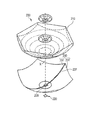
- FIG. 20 is a second example of a conventional solar cell (see Patent Document 2).
- a solar cell 200 shown in FIG. 20 includes an optical component that collects sunlight and a primary mirror 230 that is integrated with the optical component 210.
- the optical component 210 is composed of a Cassegrain type glass lens.
- the primary mirror 230 is composed of two metal films 231 and 234 arranged with a gap 237 therebetween.
- the primary mirror 230 is formed in a bowl shape.
- the flat part at the bottom of the primary mirror 230 has an opening 239.
- the opening 239 is a passage of the concentrated sunlight.
- a solar battery cell 220 that receives sunlight that has passed through the opening 239 is fixed to the outside of the bottom of the primary mirror 230.
- one of the double-sided electrodes is connected to the wiring by a die bonding method, and the other electrode is connected to the wiring by a wire bonding method.
- FIG. 21 shows a solid transparent optical panel 300 that is an assembly of the solar cells 200 shown in FIG.
- the optical component 210 of the solar cell 200 has a hexagonal shape.
- a plurality of optical components 210 (210-1 to 210-7) are adjacent to each other to form a single panel-like assembly.
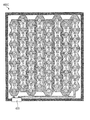
- FIG. 22 shows a concentrating light energy collecting unit 400C that is an assembly of the solar cells 200 shown in FIG.
- the solar cells 200 are connected to each other by metal films 900-11 to 900-87. That is, one P-side electrode and the other N-side electrode of two adjacent solar cells 200 are electrically connected.
- the concentrating light energy collecting unit 400C is configured by connecting a plurality of solar cells 200 in series. The electric power generated by the concentrating optical energy collecting unit 400C is taken out by the socket connector 420.
- Patent Document 3 discloses a take-out electrode structure for a thin-film solar cell in which a first electrode and a second electrode are electrically connected through a conduction groove provided in a laminated strip. According to this invention, the area of the extraction electrode portion can be reduced. However, this electrode structure is provided on the first electrode extended from the connection terminal portion of a plurality of solar cells connected in series, and improves the solar light receiving area of each solar cell. It wasn't reached.
- Patent Document 4 a lower electrode (back electrode) of each solar cell (dandem photoelectric conversion cell) and a transparent electrode (light-receiving surface electrode) of a solar cell adjacent thereto are electrically connected via a grid electrode.
- a solar cell module comprising a plurality of solar cells joined together is disclosed. According to this invention, a plurality of solar cells can be joined in series by the grid electrode. However, the solar light receiving area of each solar battery cell has not been improved.
- Patent Document 5 describes a solar cell including a condensing lens, a solar cell element, and a columnar optical member. The light condensed by the condenser lens is guided to the solar cell element through the columnar optical member.
- Patent Document 6 discloses a solar cell module in which a plurality of unit cells in which a thin film silicon photoelectric conversion unit and a compound semiconductor photoelectric conversion unit are stacked are connected in series.
- the solar cell of the conventional multi-junction compound solar cell has a surface electrode made of a metal material such as Au, Ni, or Ge that does not transmit sunlight on the surface of the top cell. Therefore, the amount of sunlight entering the solar battery cell has been reduced. Therefore, the solar power generation efficiency of the solar battery cell may be reduced.
- the condensing lens is provided apart from the solar cell. Therefore, the heat of the condensing lens generated by sunlight is difficult to dissipate, and there is a high possibility that the condensing lens is thermally deteriorated. Therefore, it is necessary to use a light condensing lens for the condensing lens, or to provide a heat sink for heat dissipation.
- An object of the present invention is to provide a solar cell having a short production lead time, excellent heat dissipation, and high power generation efficiency.
- a substrate having a plate-like base having heat dissipation, and a first conductive line and a second conductive line that are disposed on the base and are electrically separated from each other;
- a cell stack including a lower electrode joined and electrically connected to the first conductive line; a bottom cell layer disposed on an upper surface of the lower electrode; and a top cell layer disposed on an upper surface of the bottom cell layer;
- a plurality of multi-junction solar cells comprising: a transparent electrode disposed on an upper surface of the top cell layer; and a conductor connecting the transparent electrode to the second conductive line;
- a solar cell comprising: a glass plate bonded to one surface via an adhesive on the transparent electrode of the cell; and a condensing lens disposed via the transparent adhesive on the other surface of the glass plate.
- a substrate having a plate-like base having heat dissipation, and a first conductive line and a second conductive line that are disposed on the base and are electrically separated.
- a cell stack including a lower electrode, a bottom cell layer disposed on an upper surface of the lower electrode, a top cell layer disposed on the upper surface of the bottom cell layer, and an upper surface of the top cell layer.
- a step of preparing a plurality of multi-junction solar cells the step of preparing a glass plate, and a step of preparing a glass plate; Bonding the upper surfaces of the transparent electrodes of the plurality of solar cells to the surface, and fixing the plurality of multi-junction solar cells to the glass plate; and electrically connecting the lower electrode to the first conductive wire And the conductor on the second conductive wire Mounting the plurality of multi-junction solar cells on the substrate so as to be electrically connected; preparing a sheet-like condensing lens having a plurality of condensing
- a solar cell having a short production lead time, excellent heat dissipation, and high power generation efficiency is provided.
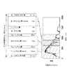
- FIG. 1 is a schematic cross-sectional view of a solar cell according to an embodiment.
- FIG. 2 is an enlarged view of a schematic cross-sectional view of the solar cell according to the embodiment.
- FIG. 3 is a diagram schematically showing the configuration of the solar battery cell according to the embodiment.
- FIG. 4 is a diagram illustrating a schematic configuration of the cell stack according to the embodiment and an absorption wavelength in each cell layer.
- FIG. 5A, FIG. 5B, FIG. 5C, and FIG. 5D are diagrams showing steps for preparing solar cells in the method for manufacturing a solar cell according to the embodiment.
- FIG. 6A, FIG. 6B, and FIG. 6C are diagrams showing steps for preparing solar cells in the method for manufacturing a solar cell according to the embodiment.
- FIG. 7A, Drawing 7B, and Drawing 7C are figures showing a process of preparing a photovoltaic cell in a manufacturing method of a photovoltaic cell concerning an embodiment.
- FIG. 8A, FIG. 8B, and FIG. 8C are figures which show the process of preparing the photovoltaic cell in the manufacturing method of the photovoltaic cell which concerns on embodiment.
- FIG. 9A, FIG. 9B, FIG. 9C, and FIG. 9D are diagrams showing a process of preparing (b-5) solar cell in the method for manufacturing a solar cell according to the embodiment.
- Drawing 10 is a figure showing the process of preparing the glass plate in the manufacturing method of the photovoltaic cell concerning an embodiment.
- FIG. 8A, FIG. 8B, and FIG. 8C are figures which show the process of preparing the photovoltaic cell in the manufacturing method of the photovoltaic cell which concerns on embodiment.
- FIG. 9A, FIG. 9B, FIG. 9C, and FIG. 9D are diagrams showing a
- FIG. 11 is a diagram illustrating a process of bonding a glass plate and a solar battery cell in the method for manufacturing a solar battery cell according to the embodiment.
- FIG. 12 is a diagram illustrating a process of mounting the solar battery cell on the substrate in the solar battery manufacturing method according to the embodiment.
- FIG. 13 is a figure which shows the process of mounting a photovoltaic cell in the board
- FIG. 14 is a diagram illustrating a process of mounting the solar battery cell on the substrate in the solar battery manufacturing method according to the embodiment.
- FIG. 15 is a diagram illustrating a process of mounting the solar battery cell on the substrate in the solar battery manufacturing method according to the embodiment.
- FIG. 16 is a diagram illustrating a process of bonding a compound eye lens to a glass plate in the method for manufacturing a solar battery cell according to the embodiment.
- FIG. 17 is a diagram illustrating a process of bonding a compound eye lens to a glass plate in the method for manufacturing a solar battery cell according to the embodiment.
- FIG. 18 is a diagram illustrating an installation state of the solar cell according to the embodiment. It is a figure which shows schematically the structure of the 1st example of the conventional solar cell. It is a figure which shows schematically the structure of the 2nd example of the structure of the conventional solar cell. It is a figure which shows schematically the structure of the 3rd example of the structure of the conventional solar cell. It is a figure which shows schematically the structure of the 4th example of the structure of the conventional solar cell.
- FIG. 1 is a schematic cross-sectional view of a solar cell according to an embodiment.
- FIG. 2 is a partial cross-sectional view of the solar cell according to the embodiment.
- the solar cell according to the embodiment includes (1) a substrate 24, (2) a plurality of (two) multi-junction solar cells 10 mounted on the substrate 24, and (3) A glass plate 34 disposed on the transparent electrode 12 of the solar battery cell 10 via a transparent adhesive, and (4) a condenser lens disposed on the glass plate 34 via a transparent adhesive 35. 31.
- the substrate 24 is disposed on the plate-like base 27 having heat dissipation, the first insulating layer 26 disposed on the base 27, and the first insulating layer 26. Electrically insulated first conductive wire 25a and second conductive wire 25b.
- the heat dissipation of the base 27 is expressed by, for example, thermal conductivity.
- the thermal conductivity of the base 27 is preferably 1.0 W / (m ⁇ K) or more and more preferably 2.0 W / (m ⁇ K) or more from the viewpoint of effectively releasing the heat of the lens. More preferred.
- the thermal conductivity of the base 27 is preferably 2 to 8 W / (m ⁇ K), for example.
- the base 27 examples include a metal plate and a ceramic plate having heat dissipation.
- the base 27 can be an aluminum base substrate or an iron base substrate.
- the thickness of the base 27 is preferably 1.0 to 1.5 mm, for example.
- the first conductive line 25a and the second conductive line 25b are electrically independent from each other.
- the first conductive line 25a and the second conductive line 25b can be formed on the base 27 by a normal method of forming a conductive layer such as a metal layer in a desired shape.
- the thickness of the first conductive line 25a and the second conductive line 25b is preferably 18 to 36 ⁇ m from the viewpoint of voltage resistance.
- the first conductive line 25a and the second conductive line 25b are composed of, for example, a copper layer having a desired planar shape and a Ni—Au layer by Ni or Au plating.
- the copper layer has a thickness of 10 to 50 ⁇ m, for example.
- the Ni—Au layer is formed by flash Au plating or electrolytic Au plating.
- the maximum thickness of the Ni—Au layer is, for example, 0.5 ⁇ m.
- the first conductive line 25a and the second conductive line 25b are electrically independent from each other.
- the first conductive wire 25 a is electrically connected to a later-described center electrode 16 b in the solar battery cell 10.
- the second conductive wire 25 b is electrically connected to a side electrode 16 described later in the solar battery cell 10.
- the substrate 24 may further have an insulating layer (hereinafter also referred to as “first insulating layer 26”) on the surface of the base 27.
- the first insulating layer 26 may be formed on the entire surface of the base 27, or may be formed only around the first conductive line 25a and the second conductive line 25b from the viewpoint of improving heat dissipation.
- the first insulating layer 26 can be formed by a normal method of forming a desired planar layer on the plate-like member. Examples of the material of the first insulating layer 26 include an epoxy resin, a phenol resin, a fluorine resin, a polyimide resin, a silicone resin, and an acrylic resin.
- the thickness of the first insulating layer 26 is 15 ⁇ m to 300 ⁇ m from the viewpoint of sufficiently ensuring the insulation and heat transfer between the conductive wire and the base 27 described above. Preferably there is.
- the first insulating layer 26 is formed by applying the insulating layer material paint to the base 27.
- the first insulating layer 26 is formed to prevent air from entering and to prevent defects such as pinhole defects in order to maintain electrical insulation.
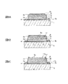
- the solar cell 10 includes a lower electrode 9a joined to and electrically connected to the first conductive wire 25a; a bottom cell layer B disposed on the upper surface of the lower electrode 9a.
- a cell stack 50 including a middle cell layer M disposed on the upper surface of the bottom cell layer B, and a top cell layer T disposed on the upper surface of the middle cell layer M; transparent disposed on the upper surface of the top cell layer T
- Side electrode 16a is
- the cell laminate 50 only needs to have the bottle cell layer B and the top cell layer T. That is, the middle layer M in the cell stack 50 may be omitted.
- the photovoltaic cell 10 may have a conductor that connects the transparent electrode 12 to the second conductive line 25b instead of the side electrode 16a.
- the conductor is, for example, a wire for wire bonding.
- the lower electrode 9a is electrically connected to the first conductive line 25a, but may be in contact with the first conductive line 25a or may be connected to the first conductive line 25a via a conductive member.
- the side electrode 16a is also electrically connected to the second conductive line 25b, but may be in contact with the second conductive line 25b or connected to the second conductive line 25b via a conductive member. .
- the solar battery cell 10 may have a further member as long as the effect of the present invention is obtained.
- the central electrode 16b may be provided on the lower surface of the lower electrode 9a in order to improve the electrical contact between the lower electrode 9a and the first conductive wire 25a.
- a lower contact layer 2b may be provided between the lower electrode 9a and the bottom cell layer B.
- an upper contact layer 2 a may be provided between the top cell layer T and the transparent electrode 12.
- the material of the contact layer can be appropriately selected according to the material of the top cell layer T and the bottom cell layer.
- an Au / Ti laminated film (not shown) may be provided between the second insulating layer 17 and the side electrode 16a. Moreover, you may have the upper electrode 9b which electrically connects the transparent electrode 12 and the side electrode 16a.
- the transparent electrode (ZnO) 12 provided on the upper surface of the upper contact layer 2a of the cell stack 50 extracts the potential of the top cell layer T.
- the upper electrode 9 b is connected to the transparent electrode 12.
- the side electrode 16a is connected to the upper electrode 9b.
- the insulating layer 17 is a silicon nitride film or the like.
- the lower surface of the side electrode 16a is disposed below the lower surface of the lower electrode 9a. More preferably, the lower surface of the side electrode 16a and the lower surface of the central electrode 16b are coincident with each other by a broken line LL. That is, it is preferable that an electrical connection portion (an electrical connection portion having a potential of the top cell and an electrical connection portion having a potential of the bottom cell) with the outside is drawn out on one surface.
- the solar battery cell 10 when the solar battery cell 10 is mounted on the substrate 24 (see FIG. 12 and FIG. 13), the solar battery cell 10 can be prevented from being damaged even when pressure is evenly applied to the solar battery cell 10. That is, when the side electrode 16a having the potential generated in the top cell layer T and the central electrode 16b having the potential generated in the bottom cell layer B are arranged on the same surface, the production process for mounting with the external electrode is one. It's time. Therefore, production lead time is shortened.
- the lower surface of the side electrode 16a and the lower surface of the central electrode 16b arranged on the same plane are electrically connected to the first conductive line 25a and the second conductive line 25b of the substrate 24 with or without a conductive member, respectively.
- the side electrode 16a and the center electrode 16b are disposed electrically independently from each other.
- the electrical connection between the lower electrode 9a and the first conductive line 25a and the electrical connection between the side electrode 16a and the second conductive line 25b are performed via an anisotropic conductive material 36. ing.
- the anisotropic conductive material 36 is, for example, a thermosetting resin film (ACF) or anisotropic conductive paste (ACP) in which conductive fine particles are dispersed.
- the gap between the substrate 24 and the glass plate 34 is preferably sealed with a sealing resin 22.
- a sealing resin 22 increases the structural strength of the structure composed of the substrate 24, the solar battery cell 10, and the glass plate 34.
- the sealing resin 22 include an epoxy resin, a phenol resin, a fluorine resin, a polyimide resin, a silicone resin, and an acrylic resin.
- the lower electrode 9a and the upper electrode 9b are conductive members such as metal.
- the lower electrode 9a and the upper electrode 9b are, for example, Au plating films having a thickness of about 10 ⁇ m.
- the center electrode 16b and the side electrode 16 are, for example, Au plating films having a thickness of about 10 to 50 ⁇ m.
- the center electrode 16b and the side electrode 16 are formed thicker than the lower electrode 9a and the upper electrode 9b.
- the second insulating layer 17 is, for example, a SiN film having a thickness of about 1 ⁇ m.
- the transparent electrode 12 is, for example, a ZnO layer having a thickness of about 0.5 ⁇ m.
- the thickness of the Au / Ti laminated film is about 0.5 ⁇ m.
- the width A of the transparent electrode 12 is, for example, 500 ⁇ m.
- the width B of the upper contact layer 2a is, for example, 470 ⁇ m.
- the width C of the peripheral edge of the transparent electrode 12 is, for example, 15 ⁇ m.
- the width of the upper electrode 9b disposed at the center of the peripheral edge is, for example, 5 ⁇ m.
- the width of the gap between the upper electrode 9b and the cell stack 50 is, for example, 5 ⁇ m.
- the width between the upper electrode 9b and the edge of the transparent electrode 12 is, for example, 5 ⁇ m.
- the thickness of the cell stack 50 is, for example, 10 ⁇ m.
- the thickness D of the solar battery cell 10 is, for example, 25 ⁇ m.
- the cell stack 50 includes an upper contact layer 2a, a top cell layer T, a tunnel layer 19a, a middle cell layer M, a tunnel layer 19b, a grid layer 20, a buffer layer 21, a bottom cell layer B, and a lower contact. Layer 2b. As described above, the middle cell layer M may be omitted.
- the forbidden bandwidth of the top cell layer T is 1.87 eV, and the wavelength that can be absorbed in the sunlight spectrum is a region of 650 nm or less.
- the forbidden band width of the middle cell layer M is 1.41 eV, and the wavelength that can be absorbed in the sunlight spectrum is in the region of 650 nm to 900 nm.
- the forbidden band width of the bottom cell layer B is 1.0 eV, and the wavelength that can be absorbed in the sunlight spectrum is in the range of 900 nm to 1,200 nm.
- the transparent electrode 12 is formed on the top cell layer T of the cell stack 50.
- the transparent electrode 12 can be formed by a normal method of forming the transparent electrode 12 at a desired position.
- Examples of the material of the transparent electrode 12 include zinc oxide (ZnO), ITO, IZO, and a graphene transparent conductive film.
- the insulating layer 17 (hereinafter also referred to as “second insulating layer”) in the solar battery cell 10 is formed on the side surface of the cell stack 50.
- the second insulating layer 17 may be formed from the side surface of the cell stack 50 to the side surface of the lower electrode 9a.
- Examples of the material of the second insulating layer 17 include SiN, BN, SiO, and the same material as the first insulating layer 26.
- the side electrode 16 a is formed on the second insulating layer 17 on the side of the cell stack 50.
- the side electrode 16 a may be formed away from the second insulating layer 17.
- the material of the side electrode 16a the material of the lower electrode 9a can be used. It is preferable that the side electrode 16a is formed to the side of the lower electrode 9a (but away from the lower electrode) from the viewpoint of being more easily electrically connected to the conductive wire on the substrate surface.
- a polytetrafluoroethylene (PTFE) layer in the “water-repellent region”; and to modify the glass plate surface so as to have a hydroxy group (—OH) in the “hydrophilic region”.
- Photolithography may be used to form the “hydrophilic region and water-repellent region”. For example, by patterning using a photosensitive resist and performing wet etching on the patterned region, the “hydrophilic region and the water repellent region” can be formed.
- the glass plate 34 may be a glass material such as soda lime glass, alkali borosilicate glass, alkali-free glass, quartz glass, low expansion glass, zero expansion glass, or crystallized glass that is generally sold for solar cells. .
- the glass plate 34 may be various tempered glass such as TFT glass, PDP glass, optical filter base glass, template glass, chemically tempered glass, and the like.
- the lens 31 is bonded to the glass plate 34 via an adhesive.
- the lens 31 has a condensing point.
- the condensing point may be in any one of the cell stacks 50 or at any position other than the cell stack 50.
- the condensing point may be on the surface of the transparent electrode, or may be on the surface opposite to the incident surface of the lens.
- the lens 31 is usually a plano-convex lens having a light receiving surface as a curved surface.
- the lens 31 is preferably a compound eye lens, and the compound eye lens has a plurality of condensing points on the side opposite to the light receiving surface.
- the lens 31 is made of a transparent material.
- the material of the lens 31 include glass and transparent resin.
- the transparent resin can be, for example, an acrylic resin, a silicone resin, or a polycarbonate resin. From the viewpoint of heat resistance, an inorganic material such as glass is preferable. On the other hand, a transparent resin is preferable from the viewpoint of weight reduction. Among these, an acrylic resin is more preferable from the viewpoints of productivity and economy.
- the lens 31 is, for example, a compound eye lens composed of a plurality of plano-convex lens portions arranged on a plane. Each plano-convex lens preferably has a condensing point on the transparent electrode 12 of the solar battery cell 10 on the surface opposite to the light incident surface, for example.
- the planar shape of the lens 31 is a square having a side length of about 50 mm.
- the thickness of the lens 31 is 7 mm, for example.
- the size of each lens and the number of condensing points in the lens 31 are set by the condensing magnification of each lens. For example, when the condensing magnification of each lens is 400 times, the size of each lens is 10 mm square. Therefore, the lens 31 has 25 (5 ⁇ 5) lenses. When the condensing magnification of each lens is 1,000 times, the size of each lens is 16 mm square. Therefore, the lens 31 has nine (3 ⁇ 3) lenses.
- the transparent resin contains, for example, an ultraviolet absorber. For this reason, even if the lens 31 is left under sunlight for a long period of time, the lens 31 does not turn yellow and can ensure transparency.
- the lens 31 is preferably a lens shape having a curved surface utilizing light refraction, or a Fresnel lens. It is preferable that the lens 31 is a compound eye lens in which a plurality of multi-junction solar cells are arranged on a single substrate and each of the transparent electrodes of the plurality of multi-junction solar cells has a condensing point.
- the lens 31 has a recess in a part of the boundary area with the transparent adhesive.
- the recess is preferably provided in a region other than the region where light is transmitted.
- the concave portion can secure the bubbles in the transparent adhesive and prevent the bubbles from flowing into the light transmitting portion of the lens.
- the transparent adhesive 35 is used for adhesion between the lens 31 and the glass plate 34 and adhesion between the glass plate 34 and the solar battery cell 10. Specifically, the transparent electrode 12 of the solar battery cell 10 is bonded to one surface of the glass plate 34 with a transparent adhesive 35; the surface opposite to the light receiving surface of the lens 31 is the other surface of the glass plate 34. It is glued to.
- the transparent adhesive 35 is made of an epoxy material or a silicone material.
- a two-component adhesive composed of a main agent made of a resin material and a curing agent made of a resin material and mixed with the main agent, or a resin material that is cured by ultraviolet rays is used.
- the solar cell according to the embodiment may have a configuration in which a plurality of the single structures described above are integrated.
- a compound eye lens in which a plurality of solar battery cells 10 are mounted on one substrate 24 and each of the plurality of transparent electrodes 12 has a condensing point may be used as the lens 31.
- substrate 24 with which the several photovoltaic cell 10 is mounted has the 1st conductive wire 25a and 2nd electroconductivity in the arrangement position of each photovoltaic cell 10.
- the compound eye lens can be constituted by, for example, a frame assembly in which a plurality of cylindrical frames are bundled, and a plano-convex lens arranged in each frame.
- a compound eye lens can be comprised by the lens formed in the shape where the some plano-convex lens was paralleled, for example.
- the solar cell according to the embodiment includes a side electrode and a base. Heat on the incident surface side (for example, lens) of the solar battery cell is transmitted to the base via the side surface electrode. Since the base has heat dissipation properties, the transmitted heat is quickly released to the outside. Therefore, the solar cell according to the embodiment has excellent heat dissipation.
- a plurality of solar cells bonded to a flat glass plate with little thickness variation are mounted on a substrate. That is, a plurality of solar cells can be mounted in a lump, and it is not necessary to mount each solar cell individually. Therefore, the production lead time can be shortened.
- the solar cell according to the embodiment does not have a surface electrode on the surface of the top cell. Therefore, according to the present invention, the solar light receiving area of the solar battery cell can be increased.
- the solar cell manufacturing method includes (1) a step of preparing a substrate, (2) a step of preparing a plurality of multi-junction solar cells, (3) a step of preparing a glass plate, and (4) a glass plate.
- a step of adhering a plurality of solar cells (5) a step of mounting a plurality of solar cells adhered to a glass plate on a substrate, and (6) a sheet-like shape having a plurality of condensing points.
- substrate 24 has the 1st conductive line 25a and the 2nd conductive line 25b which are arrange
- Each conductive line can be formed by an ordinary method for forming a metal layer having a desired planar shape.
- the base 27 has conductivity, the first insulating layer 26 is formed between the base 27 and the conductive wire.
- a disk-shaped GaAs substrate 1 (wafer) shown in FIG. 5A is prepared.
- the size of the GaAs substrate 1 is, for example, 4 inches (10.16 cm) in diameter and 500 ⁇ m in thickness.
- a plurality of solar cells 10 are formed on one GaAs substrate 1.
- a cell stack 50 is formed on a GaAs substrate 1 with a sacrificial layer 4 interposed therebetween.
- the cell stack 50 includes, for example, the upper contact layer 2a, the top cell layer T, the tunnel layers 19a and 19b, the middle cell layer M, the grid layer 20, the buffer layer 21, and the bottom cell layer B.
- the lower contact layer 2b are formed on the sacrificial layer 4 by epitaxial growth.
- the height of the obtained cell stack 50 is, for example, 10 ⁇ m.
- the cell stack 50 is obtained by forming each metal layer on the GaAs substrate 1.
- Each metal layer can be put into a vertical MOCVD (Metal Organic Chemical Vapor Deposition) apparatus, and each metal layer can be formed by an epitaxial growth method.
- MOCVD Metal Organic Chemical Vapor Deposition
- each metal layer can be performed using a normal method.
- the environmental temperature is set to about 700 ° C.
- TMG trimethylgallium
- AsH3 arsine
- TMI trimethylindium
- TMG trimethylindium
- PH3 phosphine
- SiH 4 monosilane
- DEZn diethyl zinc
- DEZn diethyl zinc
- An AlAs layer having a thickness of about 100 nm is epitaxially grown as a sacrificial layer 4 on the GaAs substrate 1.
- an n-type InGaP layer having a thickness of about 0.1 ⁇ m is grown as the upper contact layer 2a.
- the top cell layer T is formed. About 25 nm thick n-type InAlP layer as window, about 0.1 ⁇ m thick n-type InGaP layer as emitter, about 0.9 ⁇ m thick p-type InGaP layer as base, and about 0.1 ⁇ m as BSF Each of the p-type InGaP layers is formed by epitaxial growth. As a result, a top cell layer T having a thickness of about 1 ⁇ m is formed.
- a p-type AlGaAs layer having a thickness of about 12 nm and an n-type GaAs layer having a thickness of about 20 nm are grown as the tunnel layer 19.
- a tunnel layer 19 having a thickness of about 30 nm is formed.
- the middle cell layer M is formed.
- the p-type InGaP layer having a thickness of about 50 nm is formed by an epitaxial growth method.
- a middle cell layer M having a thickness of about 3 ⁇ m is formed.
- a p-type AlGaAs layer having a thickness of about 12 nm and an n-type GaAs layer having a thickness of about 20 nm are grown as the tunnel layer 19.
- a tunnel layer 19 having a thickness of about 30 nm is formed.
- the grid layer 20 suppresses the generation of dislocations and defects due to lattice constant mismatch.
- Eight n-type InGaP layers having a thickness of about 0.25 ⁇ m are formed, and a grid layer 20 having a thickness of about 2 ⁇ m is formed. Further, an n-type InGaP layer having a thickness of about 1 ⁇ m is formed as the buffer layer 21.
- the bottom cell layer B is formed.
- a p-type InGaP layer having a thickness is formed by an epitaxial growth method.
- a bottom cell layer B having a thickness of about 3 ⁇ m is formed.
- a p-type InGaAs layer having a thickness of about 0.1 ⁇ m is grown as the lower contact layer 2b.
- the lower contact layer 2b having a thickness of about 0.1 ⁇ m is patterned to a predetermined size. Patterning can be performed by dry etching.
- the cell stack 50 having a thickness of 10 ⁇ m is patterned into a predetermined planar shape.
- the size of the planar shape by patterning (for example, a circular diameter or a rectangular length) is, for example, 500 ⁇ m.
- the patterning is preferably performed by a dry etching process. It has been confirmed that by disposing the cell stack 50 on the inner side of the outer edge of the GaAs substrate 1, the disappearance of carriers generated around the solar cell portion is suppressed and the conversion efficiency is improved. Thus, the structure obtained by etching the cell stack at the edge portion is sometimes referred to as a “Ledge structure”. ⁇ J. Vac. Sci. Technol. B, Vol.
- an Au plating electrode is formed as the upper electrode 9b and the lower electrode 9a.
- an Au plating film having a thickness of about 10 ⁇ m or less is formed on the entire upper surface of the cell stack 50 of FIG. 5D by electroplating.
- the Au plating film is patterned to form an upper electrode 9b and a lower electrode 9a. The patterning is performed by combining photolithography and wet etching.
- a SiN film as the insulating layer 17 is formed.
- a SiN film is formed on the entire upper surface of the cell stack using a plasma CVD method.
- an Au / Ti laminated film is formed on the entire upper surface of the cell laminated body obtained in FIG. 6C by using a metal sputtering method.
- the Au / Ti laminated film becomes a pretreatment film for performing electrolytic Au plating in the next step.
- a portion where it is not necessary to form an electrolytic Au plating film is covered with a resist 18.
- a resist 18 for mesa etching is used to cover a portion where it is not necessary to form a plating film through an exposure process and etching with an alkaline aqueous solution or an acid solution. Thereafter, an electrolytic Au plating film is formed.
- the central electrode 16b and the side electrode 16a are formed by electrolytic Au plating.
- the central electrode 16b and the side electrode 16a made of an Au plating film are formed to a thickness of about 10 to 50 ⁇ m, which is larger than the thickness of the cell stack of solar cells.
- the Ti film may be formed by metal sputtering, and is formed on the entire upper surface of the stacked body obtained in FIG. 5B.
- the resist 18 (FIG. 7C) is removed.
- the resist 18 is removed by wet processing. Only the resist 18 can be removed by etching with an alkaline aqueous solution and an acid solution.
- the Au / Ti film on the insulating layer 17 and the Ti film on the Au plating electrode are removed. These removals are performed with a dry edge. In this way, the surface of the Au plating electrode is a clean surface free from organic contamination.
- FIG. 8B a basic structure of a single-sided multi-junction compound solar cell is obtained.
- the top cell layer T is on the GaAs substrate 1 side and the bottom cell layer B is on the center electrode 16b side.
- the GaAs substrate 1 In order to allow sunlight to enter from the top cell layer T, the GaAs substrate 1 must be peeled off from the basic structure of the solar battery cell shown in FIG. 8B. At that time, the solar battery cell 10 should not be damaged.
- the solar battery cell 10 should not be damaged. Therefore, as shown in FIG. 8C, after the solar cell 10 is turned upside down so that the GaAs substrate 1 side is above the direction of gravity, the solar cell 10 is placed on the holding plate 29 provided with the wax 28. . Thereafter, a sacrificial layer recess 4 a is provided on the side surface of the sacrificial layer 4 in order to peel the GaAs substrate 1. Since the solar cell 10 is very fragile, it may be destroyed by stress when the GaAs substrate 1 is peeled off.
- a sacrificial layer recess 4a is provided as a starting point for reliably breaking the sacrificial layer 4 internally.
- the sacrificial layer recess 4a may be provided by grinding with a blade, grinding with a water jet, or mechanical “scribing”.
- the solar battery cell 10 is mechanically reinforced by sealing the gap between the solar battery cell 10 and the substrate 24 with the sealing resin 22. Therefore, the solar battery cell 10 is not destroyed when the sacrificial layer recess 4a is formed.
- the sacrificial layer 4 is internally broken and the GaAs substrate 1 is peeled off.
- the internal fracture of the sacrificial layer 4 utilizes SOI (silicon on insulator) related techniques such as dicing, roller peeling, water jet, ultrasonic destruction.
- the lattice constant of GaAs constituting the substrate 1 is 5.653 angstroms
- the lattice constant of AlAs constituting the sacrificial layer 4 is 5.661 angstroms, which are almost the same. Therefore, the sacrificial layer 4 is a stable film and can be internally broken stably.
- the sacrificial layer 4 remaining in the solar battery cell 10 is removed by wet etching.
- the sacrificial layer 4 can be melted and removed by contacting with the hydrofluoric acid for 2 to 3 minutes. Since the solar battery cell 10 is protected by the sealing resin 22, hydrofluoric acid does not damage the solar battery cell 10.
- the transparent electrode 12 is formed.
- the transparent electrode 12 constitutes an incident surface for sunlight.
- the transparent electrode 12 is a ZnO layer, an ITO layer, or the like, and can be formed by a sputtering method.
- the transparent electrode 12 is formed on the entire upper surface of the solar battery cell 10, and electrically connects the upper contact layer 2a and the upper electrode 9b.
- the conductivity can be improved by adding 0.1% by mass or more of Al or Ga to the ZnO layer.
- the wax 28 is removed from the solar battery cell 10.
- the solar battery cell 10 thus obtained does not have an electrode that blocks sunlight on the sunlight incident surface. Therefore, the amount of sunlight incident on the solar battery cell 10 is increased, and the power generation efficiency of the solar battery cell 10 is improved.
- the cell stack 50 of the solar battery cell 10 is thin (for example, 10 ⁇ m or less), the GaAs substrate 1 is peeled off to give a solar battery without damaging the cell stack 50. be able to.
- a glass plate 34 is prepared.
- the glass plate 34 is flat glass or flat tempered glass having a thickness of 2 to 10 mm. It may be a glass plate used for a general solar cell.
- the liquid repellent layer 23 is provided in a predetermined region on the back surface of the glass plate 34.
- the predetermined region is a region other than a region (also referred to as “light condensing point 32”) to which the transparent electrodes of a plurality of (two or more) solar cells 10 are bonded.
- the liquid repellent treatment is a silane coupling agent having a fluorocarbon chain such as CF 3 (CF 2 ) 7 C 2 H 4 SiCl 3 or a hydrocarbon chain such as CH 3 (CH 2 ) 17 SiCl 3.
- a liquid repellent layer 23 of polytetrafluoroethylene (PTFE) may be formed.
- the region where the transparent electrodes of the plurality of (two or more) photovoltaic cells 10 are bonded is relatively lyophilic with respect to the transparent adhesive.
- the region to which the transparent electrode is bonded (the light condensing point 32) may be subjected to a lyophilic treatment that improves the wettability of the transparent adhesive.
- a transparent adhesive 35 is applied to the condensing point 32 having lyophilic properties.
- the transparent adhesive 35 is applied with a screw nozzle dispenser. Even if the viscosity of the transparent adhesive changes, a certain amount of coating is performed. In the present embodiment, a 100 to 1000 nanoliter transparent adhesive is applied using the resin application head 43, although the application amount varies depending on the element size. The transparent adhesive wets and spreads on the condensing point 32, and the liquid repellent layer 23 is not applied.
- the transparent electrode 12 of the solar cell 10 is positioned at the condensing point 32 of the glass plate 34 coated with the transparent adhesive 35. Glue together.
- the thickness of the solar battery cell 10 is as thin as 5 to 50 ⁇ m, and the solar battery cell 10 includes a compound semiconductor such as GaAs or Ge. For this reason, the photovoltaic cell 10 is very fragile. Therefore, it is necessary to bond the solar cell 10 to the glass plate 34 so as not to apply a load to the solar cell 10.
- the solar battery cell 10 is vacuum-sucked in the suction hole 42 of the planar mount head 41 and mounted on the condensing point 32.
- the mount load is about 10 to 50 gf (9.81 ⁇ 10 ⁇ 2 to 4.90 ⁇ 10 ⁇ 1 N).
- the solar battery cell 10 mounted on the condensing point 32 is aligned with the lyophilic region (that is, the condensing point) by getting wet with the transparent adhesive 35.
- the transparent electrode surface of the solar battery cell 10 is a square of 800 ⁇ m ⁇ 800 ⁇ m
- the condensing point 32 is set to a square of 900 ⁇ m ⁇ 900 ⁇ m, and the other region is a liquid repellent region.
- the solar battery cell 10 is aligned on the glass surface by the balance of the surface tension of the transparent adhesive 35, and is disposed inside the condensing point 32.
- Each of the solar cells 10 may be mounted one by one with a planar mount head 41, and a plurality of solar cells are arranged by arranging a metal mask having through holes corresponding to a plurality of condensing points on a glass plate. It is also possible to mount 10 at a condensing point in a lump. Moreover, it is also possible to apply
- the transparent adhesive 35 is cured.
- a two-component mixed room temperature curable resin is used for the transparent adhesive 35.
- the transparent adhesive 35 may be an ultraviolet curable resin.
- ultraviolet rays are irradiated after alignment and mounting of the solar battery cell 10 to the light condensing point.
- the transparent electrode 12 of the solar battery cell 10 is appropriately fixed to the condensing point of the glass plate 34.
- the water-repellent layer 23 on the glass substrate 34 is removed.
- the water repellent layer can be removed, for example, with a dry edge. Due to the dry edge, the surface of the glass plate 34 becomes lyophilic.
- the wettability with the sealing resin 22 decreases. Therefore, peeling failure occurs between the glass plate 34 and the sealing resin 22 due to the stress caused by the thermal cycle. Therefore, it is preferable to remove the water repellent layer 23 on the glass substrate 34.
- the multi-junction solar cell 10 bonded to the glass plate 34 is mounted on the substrate 24. Specifically, the multi-junction solar cell 10 is mounted on the substrate 24 by electrically connecting the lower electrode 9a to the first conductive wire 25a and electrically connecting the side electrode 16a to the second road wire 25b. To implement. The mounting position of the multi-junction solar cell 10 bonded to the glass plate 34 on the substrate 24 can be confirmed by, for example, an image of the bonding position photographed by a camera.
- ACF Anisotropic Conductive Material
- the anisotropic conductive material 36 can be a film or a paste.
- the anisotropic conductive material 36 includes an epoxy resin and conductive particles dispersed therein.
- the anisotropic conductive material 36 is mainly used for mounting a driver for driving a liquid crystal display.
- the film-like anisotropic conductive material 36 is preferably larger than the arrangement region of the solar cells 10 on the substrate 24, and has a size surrounding the second conductive line, for example.
- the thickness of the anisotropic conductive material 36 needs to be sufficiently larger than the gap between the electrode of the solar battery cell 10 and the conductive line on the substrate 24. That is, the film of the anisotropic conductive material 36 is thicker than the thickness of the first conductive line 25a and the second conductive line 25b. For example, when the thickness of the first conductive line 25a and the second conductive line 25b is 35 ⁇ m, the thickness of the anisotropic conductive material 36 can be 40 to 60 ⁇ m.
- the first conductive line 25a and the second conductive line 25b of the substrate 24 are covered with an anisotropic conductive film.
- mounting is performed by thermocompression bonding of the multi-junction solar cell 10 bonded to the glass plate 34 to the substrate 24 on which the anisotropic conductive film is disposed.
- the anisotropic conductive film may be temporarily fixed on the substrate by heating and pressurizing to such an extent that the anisotropic conductive film is partially cured. More specifically, as shown in FIG. 12, a film of anisotropic conductive material 36 is attached to the substrate 24.
- the entire anisotropic conductive material 36 is preferably heated and pressed for 5 seconds or less with a flat tool heated to 60 to 100 ° C. from the upper part and pasted. At this time, it is preferable that the anisotropic conductive material 36 is attached to the arrangement region under the condition that the epoxy resin inside the anisotropic conductive material 36 does not undergo a curing reaction.
- a plurality (two or more) of solar cells 10 bonded to a glass plate 34 are attached to a substrate 24 to which an anisotropic conductive material 36 is attached. Then, a temporary press-bonded product is obtained by positioning and mounting.
- the recognition mark attached to the glass plate 34 and the recognition mark on the substrate 24 are recognized by the CCD camera, and the solar battery cell 10 is arranged at a predetermined position on the substrate 24 using the position information.
- the temporary pressure bonding of the solar battery cell 10 is performed at a normal temperature and a low load. Therefore, the electrode of the solar battery cell 10 and the conductive wire of the substrate 24 are not electrically connected.
- the solar cells 10 are electrically connected to the substrate 24 and the solar cells 10 are fixed to the substrate 24.
- the temporary press-bonded product obtained by the above-described temporary press-bonding process is placed on the metal stage with the substrate 24 facing down.
- a protective sheet 39 in the form of a film of polytetrafluoroethylene or polyimide material is placed from above the glass plate 34.
- the temporary pressure-bonded product is pressed through the protective sheet 39 with a metal heating and pressing head 40 heated to about 180 to 220 ° C.
- the load per solar cell is about 50 to 200 gf (0.49 to 1.96 N), and the pressurization time is 5 to 20 seconds.
- This pressure causes the epoxy resin inside the anisotropic conductive material 36 to melt and then harden.
- the central electrode 16 b of the solar battery cell 10 is electrically connected to the first conductive wire 25 a of the substrate, and the side electrode 16 of the solar battery cell 10 is electrically connected to the second conductive wire 25 b of the substrate 24.
- the electrical connection is through conductive particles in the anisotropic conductive material 36.
- the solar battery cell 10 is electrically connected to the first conductive wire 25a and the second conductive wire 25b, and the solar battery cell 10 and the substrate are physically fixed.
- FIG. 14 shows the structure of the solar battery cell after the main pressure bonding step.
- the thickness variation of the glass plate 34 is as small as 10 ⁇ m or less, and the thickness of the substrate 24 is also small. Therefore, a plurality of solar cells 10 having a thickness of 10 ⁇ m or less can be stably mounted on the substrate 24 at once.
- the sealing resin 22 is usually an epoxy resin or a silicone resin.
- Examples of the sealing resin 22 include a two-component adhesive containing a main agent and a curing agent, a resin material that is cured by ultraviolet rays, and a resin material that is cured by heating.
- the difference between the linear expansion coefficient of the glass plate 34 and the linear expansion coefficient of the substrate 24 causes the anisotropic conductive material 36 to be used. Stress concentrates on the bonded part.
- the sealing resin 22 filled in the gap 50 between the substrate 24 and the glass plate 34 can reduce this stress concentration.
- the gap 50 between the substrate 24 and the glass plate 34 is usually filled with the sealing resin 22 by placing the substrate 24 on a metal stage heated to 50 to 80 ° C. and placing the liquid sealing resin 22 in the gap 50. It is performed by a method of pouring using a capillary phenomenon.
- the sealing resin 22 is cured by heating at about 150 to 200 ° C. for about 15 minutes to 1 hour.
- the sealing resin 22 is applied onto the substrate 24 before the temporary press-bonding step, and the gap 50 is filled with the sealing resin 22 by heating and pressurizing in the main press-bonding step, and heating in the main press-bonding step.
- the sealing resin 22 may be cured by the above. According to this method, the electrical connection between the solar cell 10 and the first conductive line 25 a and the second conductive line 25 b and the sealing of the gap with the sealing resin 22 can be performed simultaneously.
- the sealing resin 22 When the sealing resin 22 is filled in the gap 50 between the substrate 24 and the glass plate 34, the sealing resin 22 is naturally cured at a temperature of 80 ° C. or lower (for example, normal temperature (20 ⁇ 15 ° C.)). Alternatively, the sealing resin 22 is cured by irradiating ultraviolet rays.
- the sheet-like condensing lens which has several condensing points is prepared.
- the condensing lens is preferably a compound eye lens having a plurality of condensing points on the surface opposite to the light incident surface.
- a transparent adhesive 35 is applied to the glass plate 34.
- the transparent adhesive 35 can be applied using a dispensing method, a printing method, a spin coating method, or the like.
- the transparent adhesive 35 can be the same as the adhesive for bonding the solar battery cell 10 to the glass plate 34.
- the lens 31 is bonded and fixed to the glass plate 34 with a transparent adhesive 35.
- a concave portion 31a may be provided in a part of the boundary region between the lens 31 and the transparent adhesive.
- the recess 31a is preferably provided in a region other than the light transmission portion.
- the concave portion 31a takes in the air bubbles contained in the transparent adhesive and prevents the air bubbles from flowing into the light transmitting portion of the lens 31. In this way, the light transmitted through the lens 31 is suppressed from being reflected by the air bubbles and the efficiency as a solar cell is reduced.
- the lens 31 and the glass plate 34 may be bonded together under reduced pressure or under pressure so that no air remains in the transparent adhesive 35.
- the transparent adhesive 35 may be applied to the central portion of the glass plate 34, and the transparent adhesive 35 may be spread while the lens 31 is pressed against the glass plate 34, so that no air remains in the transparent adhesive 35.
- the plurality of solar battery cells 10 are attached to the other surface of the glass plate 34, and the lens 31 that is a compound eye lens is attached to one surface of the glass plate 34.
- each condensing point of a compound eye lens is set to the photovoltaic cell 10, Preferably it sets to the transparent electrode 12.
- FIG. 18 shows a solar cell according to an embodiment including a plurality of solar cells 10 attached to one surface of a glass plate and a compound eye lens 31 attached to various surfaces of the glass plate. .
- a heat radiating member 37 is disposed on the lower surface of the substrate 24 of the solar cell via a heat radiating resin 44.
- the solar cell in FIG. 18 When the solar cell in FIG. 18 is placed under sunlight, sunlight 30 is irradiated onto the lens 31 along the direction of the arrow. Sunlight incident on the lens 31 is preferably transmitted through the transparent adhesive 35 and the glass plate 34, collected by the transparent electrode 12, and incident on the cell stack 50. The light that has passed through the transparent electrode 12 passes through the top cell layer T, middle cell layer M, and bottom cell layer B in the cell stack. And the light according to the absorption wavelength of each cell layer in sunlight is converted into an electromotive force in each cell layer. For example, the conversion efficiency in the solar battery cell 10 is about 30 to 50%.
- the lens 31 may be heated by infrared rays contained in sunlight.
- the heat of the lens 31 is quickly transmitted to the substrate 24 through the glass plate 34, the transparent electrode 12, the upper electrode 9 b, and the side electrode 16. Then, it is discharged from the substrate 24 to the outside. Therefore, the lens 31 is not easily heated.
- the glass plate 34 and the lens 31 are in close contact with the solar battery cell 10.
- the solar battery cell 10 has a side electrode 16.
- the heat of the lens 31 can be conducted to the substrate 24 through the side electrode 16.
- the base 27 of the substrate 24 has a large surface area.
- the heat conducted to the substrate 24 is released from the base 27 to the outside. Therefore, the heat of the lens 31 is easily dissipated. Therefore, the lens 31 can be molded with a transparent resin having low heat resistance.
- the material cost of the lens 31 can be reduced as compared with the case of using glass.
- the solar cell can be made lighter than in the case of using glass. Thereby, the workability
- stress may be generated in the solar cell due to heat from the lens 31.
- the stress generated in the solar cell according to the embodiment is dispersed by the sealing resin 22 filled in the gap between the substrate 24 and the lens 31. Therefore, damage to the cell stack and the solar battery cell 10 due to stress concentration on the transparent adhesive 35 and the anisotropic conductive material 36 is suppressed.
- the solar cell according to the embodiment includes solar cells whose electrodes arranged on the light receiving surface are transparent, sunlight can be efficiently taken into the solar cells.
- the solar cell according to the embodiment includes a solar cell 10 having a cell stack having a three-layer stacked structure including a top cell layer T, a middle cell layer M, and a bottom cell layer B. Therefore, it is possible to effectively photoelectrically convert light in various wavelength regions included in sunlight. Therefore, a highly efficient solar cell can be realized.
- the thickness of the solar cell (the distance from the bottom surface of the substrate 24 to the top of the lens 31) can be designed to be about 20 mm.
- the thickness of the solar cell according to the embodiment may be about 10% with respect to the thickness of the conventional solar cell in which the lens 31 is disposed apart from the solar cell 10.
- the solar cell 10 in which the electrode having the potential of the top cell layer T and the electrode having the potential of the bottom cell layer B are both disposed on the side opposite to the sunlight incident surface. It comprises.
- the solar battery cell 10 can be mounted on the substrate 24 in one step. Therefore, the production lead time of the solar cell is shortened.
- the solar battery cell in the conventional multi-junction compound solar battery has a double-sided electrode structure having a front electrode and a back electrode.
- the back electrode is often mounted in a die bonding process
- the front surface electrode is often mounted in a wire bonding process or the like. That is, in the conventional solar cell, two mounting processes, that is, mounting of the back surface electrode and mounting of the front surface electrode are required in order to achieve electrical connection with the outside. As a result, production lead time becomes longer.
- a light, thin and small solar cell can be easily manufactured with high temperature cycle resistance, high humidity resistance, and high impact resistance. Furthermore, since the electrode on the light receiving part side of sunlight passes through the side part of the solar battery cell 10 and is electrically connected to the second conductive wire 25b on the heat radiating substrate 24, the conductive path is a heat transfer path. Can be used. For this reason, the high heat dissipation of a solar cell is realizable.
- the solar cell of the present invention can be used for power generation in space and for concentrating solar cells on the earth. And the conversion efficiency of sunlight can be improved greatly compared with the conventional silicon solar cell. Therefore, it can be used as a large-scale power generation system in an area with a large amount of sunlight.
Abstract
Description
図1は、実施形態に係る太陽電池の概略断面図である。図2は、実施形態に係る太陽電池の部分断面図である。図1および図2に示されるように、実施形態に係る太陽電池は、(1)基板24と、(2)基板24に実装された、複数の(2つの)多接合型太陽電池セル10と、(3)太陽電池セル10の透明電極12上に、透明接着剤を介して配置されたガラス板34と、(4)ガラス板34上に透明接着剤35を介して配置された集光レンズ31とを有する。 <Solar cell>
FIG. 1 is a schematic cross-sectional view of a solar cell according to an embodiment. FIG. 2 is a partial cross-sectional view of the solar cell according to the embodiment. As shown in FIGS. 1 and 2, the solar cell according to the embodiment includes (1) a
図2に示されるように、基板24は、放熱性を有する板状のベース27と、ベース27上に配置された第一絶縁層26と、第一絶縁層26上に配置された電気的に絶縁された第一導電線25a及び第二導電線25bと、を有する。ベース27の放熱性は、例えば熱伝導率によって表される。ベース27の熱伝導率は、レンズの熱を効果的に放出する観点から、1.0W/(m・K)以上であることが好ましく、2.0W/(m・K)以上であることがより好ましい。ベース27の熱伝導率は、例えば2~8W/(m・K)が好ましい。 (1) Substrate As shown in FIG. 2, the
図2に示すように、太陽電池セル10は、第一導電線25aに接合されて電気接続した下部電極9aと;下部電極9aの上面上に配置されたボトムセル層B、ボトムセル層Bの上面上に配置されたミドルセル層M、およびミドルセル層Mの上面上に配置されたトップセル層Tを含むセル積層体50と;トップセル層Tの上面上に配置された透明電極12と;セル積層体50の側面に配置された絶縁層17と;透明電極12と第二導電線25bとを電気接続するように、絶縁層17を介してセル積層体50の側面に配置された側面電極16aと、を有する。 (2) Solar Cell As shown in FIG. 2, the
太陽電池セル10は、透明接着剤を介して、ガラス板34の太陽光の集光点である所定の位置に接着される。所定の位置に確実に太陽電池セル10を固定するためには、後述のように、ガラス板34表面に透明接着剤が濡れる「親水領域」と、透明接着剤をはじく「撥水領域」を形成した後に、太陽電池セル10を接着することが好ましい。 (3) About a glass plate The
レンズ31は、ガラス板34に接着剤を介して接着されている。レンズ31は、集光点を有する。集光点は、セル積層体50のいずれかにあるか、またはセル積層体50以外の任意の位置にあってもよい。例えば、集光点は透明電極の表面にあってもよいし、レンズの入射面の反対側の表面にあってもよい。 (4) Lens The
透明接着剤35は、レンズ31とガラス板34との接着と、ガラス板34と太陽電池セル10との接着とに用いられる。具体的には、太陽電池セル10の透明電極12が、ガラス板34の一方の面に透明接着剤35によって接着されており;レンズ31の受光面に対する反対面が、ガラス板34の他方の面に接着されている。 (5) About Transparent Adhesive The
さらに実施形態に係る太陽電池は、前述した単体の構造の複数が一体化した構成を有していてもよい。例えば、実施形態に係る太陽電池は、複数の太陽電池セル10が一枚の基板24に実装され、複数の透明電極12のそれぞれに集光点を有する複眼レンズをレンズ31としてもよい。複数の太陽電池セル10が実装される基板24は、各太陽電池セル10の配置位置に、第一導電線25aと第二導電性とを有する。 (6) Others Further, the solar cell according to the embodiment may have a configuration in which a plurality of the single structures described above are integrated. For example, in the solar battery according to the embodiment, a compound eye lens in which a plurality of
太陽電池の製造方法は、(1)基板を準備する工程と、(2)複数の多接合型太陽電池セルを準備する工程と、(3)ガラス板を準備する工程と、(4)ガラス板に、複数の太陽電池セルを接着する工程と、(5)ガラス板に接着された複数の太陽電池セルを、基板上に実装する工程と、(6)複数の集光点を有するシート状の集光レンズを準備する工程と、(7)集光レンズをガラス板に接着する工程とを含む。 <Method for manufacturing solar cell>
The solar cell manufacturing method includes (1) a step of preparing a substrate, (2) a step of preparing a plurality of multi-junction solar cells, (3) a step of preparing a glass plate, and (4) a glass plate. A step of adhering a plurality of solar cells, (5) a step of mounting a plurality of solar cells adhered to a glass plate on a substrate, and (6) a sheet-like shape having a plurality of condensing points. A step of preparing a condensing lens, and (7) a step of adhering the condensing lens to a glass plate.
基板24は、例えば、ベース27と、ベース27に配置され、互いに電気的に独立する第一導電線25a及び第二導電線25bを有する。各導電線の形成は、所望の平面形状の金属層を形成する通常の方法によって行うことができる。また、ベース27が導電性を有する場合には、ベース27と導電線との間に第一絶縁層26が成膜される。 (1) About the process of preparing a board | substrate The board |
まず図5Aに示す、円板状のGaAs基板1(ウェハ)を用意する。GaAs基板1のサイズは、例えば、直径が4インチ(10.16cm)、厚さが500μmである。通常、1つのGaAs基板1に複数の太陽電池セル10を形成する。 (2) Step of Preparing Solar Cell First, a disk-shaped GaAs substrate 1 (wafer) shown in FIG. 5A is prepared. The size of the
図5Bに示すように、GaAs基板1上に、犠牲層4を介してセル積層体50を形成する。セル積層体50は、図4を用いて先に説明したように、例えば上部コンタクト層2a、トップセル層T、トンネル層19a、19b、ミドルセル層M、グリッド層20、バッファ層21、ボトムセル層B、及び下部コンタクト層2bを、エピタキシャル成長によって犠牲層4上に形成することで得られる。得られるセル積層体50の高さは、例えば10μmである。セル積層体50は、GaAs基板1の上に、各金属層を形成することで得られる。各金属層は、縦型MOCVD(Metal Organic Chemical Vapor Deposition)装置に投入し、各金属層をエピタキシャル成長法によって形成されうる。 Manufacture of Cell Stack As shown in FIG. 5B, a
GaAs基板1を剥離するときに、太陽電池セル10にダメージを与えてはならない。そこで、図8Cに示すように、GaAs基板1側が重力方向の上方になるように太陽電池セル10を上下反転させた後、太陽電池セル10をワックス28が設けられた保持板29上に配置する。その後、GaAs基板1を剥離させるために、犠牲層4の側面に犠牲層凹部4aを設ける。太陽電池セル10は非常に脆弱なため、GaAs基板1を剥離するときの応力で破壊されることがある。このため、犠牲層4を確実に内部破断させるための起点として、犠牲層凹部4aを設ける。犠牲層凹部4aは、ブレードで研削したり、ウォータージェットで研削したり、機械的な「ケガキ」をするなどして設ければよい。太陽電池セル10と基板24との隙間を封止樹脂22で封止することで、太陽電池セル10が機械的に補強されている。そのため、犠牲層凹部4aを形成するときに太陽電池セル10が破壊されない。 Formation of recess in sacrificial layer When the
図9Aに示すように、犠牲層4を内部破断させて、GaAs基板1を剥離する。犠牲層4の内部破断は、ダイシング、ローラー剥離、ウォータージェット、超音波破壊などのSOI(silicon on insulator)関連の技術を利用する。 Separation of GaAs Substrate As shown in FIG. 9A, the
図9Bに示すように、太陽電池セル10に残存した犠牲層4をウェットエッチングで除去する。例えば、犠牲層4をフッ酸に2~3分間接触させて、溶融除去することができる。太陽電池セル10が封止樹脂22で保護されているので、フッ酸が太陽電池セル10にダメージを与えない。 Etching of Sacrificial Layer As shown in FIG. 9B, the
図9Cに示すように、透明電極12を形成する。透明電極12は、太陽光の入射面を構成する。透明電極12は、ZnO層やITO層などであり、スパッタ工法で形成されうる。透明電極12は、太陽電池セル10の上部全面に形成され、上部コンタクト層2aと上部電極9bとを電気的に接続する。ZnO層に、AlやGaを0.1質量%以上添加することにより、導電性を向上させることもできる。 Formation of Transparent Electrode As shown in FIG. 9C, the
(3-1)ガラス板の表面の撥液処理と親液処理
図10に示すように、ガラス板34を用意する。ガラス板34は、厚み2~10mmの平面ガラス又は平面強化ガラスである。一般的な太陽電池に用いているガラス板でありうる。 (3) Step of Preparing Glass Plate (3-1) Liquid Repellent Treatment and Lipophilic Treatment of Glass Plate Surface As shown in FIG. 10, a
図10に示すように、親液性を有する集光点32に透明接着剤35を塗布する。例えば、透明接着剤35をスクリューノズル式ディスペンサーにて塗布する。透明接着剤の粘度が変化しても、一定量の塗布を行う。素子サイズにより塗布量は異なるが、本実施例では樹脂塗布ヘッド43を用いて100~1000ナノリットルの透明接着剤を塗布する。透明接着剤は、集光点32に濡れ広がり、撥液層23は塗布されない。 (3-2) Application of Transparent Adhesive As shown in FIG. 10, a
図11に示すように、透明接着剤35を塗布されたガラス板34の集光点32に、太陽電池セル10の透明電極12を、位置合わせしながら接着する。 (4) Step of Adhering Solar Cell to Glass Plate As shown in FIG. 11, the
太陽電池セル10を接着後、ガラス基板34上の撥水層23を除去する。撥水層は、例えば、ドライエッジで除去することができる。ドライエッジにより、ガラス板34の表面は親液性となる。太陽電池セル10を接着したガラス基板34に撥水層23が残存すると、封止樹脂22(図15参照)との濡れ性が低下する。そのため、熱サイクルによる応力で、ガラス板34と封止樹脂22間で剥離不良が発生する。従って、ガラス基板34上の撥水層23を除去することが好ましい。 Removal of water-repellent layer After the
ガラス板34に接着された多接合型太陽電池セル10を基板24に実装する。具体的には、下部電極9aを第一導電線25aに電気的に接続し、かつ側面電極16aを第二道電線25bに電気的に接続することで、多接合型太陽電池セル10を基板24に実装する。ガラス板34に接着された多接合型太陽電池セル10の基板24への実装位置は、例えば、カメラによって撮影される接着位置の画像によって確認することができる。 (5) About the process of mounting a photovoltaic cell on a substrate The multi-junction
多接合型太陽電池セル10の基板24への実装は、異方性導電材料を用いて行うことが好ましい。基板24上に異方性導電材料36を配置する。そして、異方性導電材料36を介して、第一導電線25aに下部電極9aを接続し、第二導電線25bに側面電極16aを接続する。異方性導電材料を用いることで、基板24に多接合型太陽電池セル10を容易に実装することができる。 (5-1) Arrangement of Anisotropic Conductive Material (ACF) on Substrate Mounting of the multi-junction
図12に示すように、ガラス板34に接着された複数の(2以上の)太陽電池セル10を、異方性導電材料36が貼り付けられた基板24に、位置合わせしてマウントすることで仮圧着品を得る。ガラス板34に付された認識マークと、基板24上の認識マークをCCDカメラにより認識し、その位置情報を用いて、基板24の所定の位置に、太陽電池セル10が配置される。太陽電池セル10の仮圧着は、常温かつ低荷重で行う。そのため、太陽電池セル10の電極と基板24の導電線とは、電気導通しない。 Temporary Mounting of Solar Cells on Substrate As shown in FIG. 12, a plurality (two or more) of
次に、図13に示すように、太陽電池セル10を基板24に電気接続すると共に、太陽電池セル10を基板24に固定する。具体的には、まず金属ステージに、前述した仮圧着工程による仮圧着品を、基板24を下にして置く。次に、ガラス板34の上方からポリテトラフルオロエチレンやポリイミド材料のフィルム形状の保護シート39を置く。次に、180~220℃程度に加熱した金属の加熱加圧ヘッド40で、保護シート39を介して仮圧着品を加圧する。1つの太陽電池セル当たりの荷重を約50~200gf(0.49~1.96N)とし、加圧時間を5~20秒間とする。 Next, as shown in FIG. 13, the
図15に示すように、図14に示される構造物における基板24とガラス板34との隙間50を封止樹脂22で封止する。隙間50を封止樹脂22で封止することにより、パッケージの強度が保持され、耐薬品性が向上する。封止樹脂22は、通常は、エポキシ樹脂またはシリコーン樹脂である。封止樹脂22の例には、主剤と硬化剤とを含む二液性接着剤、紫外線で硬化する樹脂材料、及び、加熱で硬化する樹脂材料が含まれる。 Reinforcement with sealing resin As shown in FIG. 15, the
複数の集光点を有するシート状の集光レンズを準備する。集光レンズは、光の入射面とは反対側の表面に複数の集光点を有する複眼レンズであることが好ましい。 (6) About the process of preparing a condensing lens The sheet-like condensing lens which has several condensing points is prepared. The condensing lens is preferably a compound eye lens having a plurality of condensing points on the surface opposite to the light incident surface.
図16に示すように、ガラス板34に透明接着剤35を塗布する。透明接着剤35は、ディスペンス工法、印刷工法、スピンコート工法などを用いて塗布することができる。透明接着剤35は、太陽電池セル10をガラス板34に接着するための接着剤と同一でありうる。 (7) Step of adhering the condenser lens to the glass plate As shown in FIG. 16, a
図18には、ガラス板の一方の面に貼り付けられた複数の太陽電池セル10と、ガラス板の多様の面に貼り付けられた複眼レンズ31とを含む、実施形態に係る太陽電池を示す。太陽電池の基板24の下面には、放熱用樹脂44を介して放熱部材37が配置されている。 <Solar cell installation state>
FIG. 18 shows a solar cell according to an embodiment including a plurality of
2a 上部コンタクト層
2b 下部コンタクト層
4 犠牲層
4a 犠牲層凹部
9a 下部電極
9b 上部電極
10、120、220 太陽電池セル
12 透明電極
15 表面電極
16a 側面電極
16b 中央電極
16c Au/Ti積層膜
16d Ti膜
17 第二絶縁層
17a、17b 第二絶縁層の窓
18 レジスト
19a、19b トンネル層
20 グリッド層
21 バッファ層
22 封止樹脂
23 撥水層
24 基板
25a 第一導電線
25b 第二導電線
26 第一絶縁層
27 ベース(金属板)
28 ワックス
29 保持板
30 太陽光
31 レンズ
32 集光点
34 ガラス板
35 透明接着剤
36 異方性導電材料
37 放熱部材
38 ステージ
39 保護シート
40 加熱加圧ヘッド
41 マウンドヘッド
42 吸着穴
43 樹脂塗布ヘッド
44 放熱用樹脂
50 セル積層体
100、200 太陽電池
110 光学部品
113 凹部
124A 第1接続部
124B 第2接続部
140 バックシート
150 回路基板
153 絶縁体
154 導電体
154A、154B 電極部分
155 接着層
210 光学部品
230 一次鏡
231、234 金属膜
237 隙間
239 開口
300 固体透明光学パネル
400C 集光型光エネルギ収集ユニット
420 ソケットコネクタ
A 図1の太陽電池における太陽電池セル10の周辺を囲む線
B ボトムセル層
M ミドルセル層
T トップセル層 DESCRIPTION OF
28
Claims (15)
- 放熱性を有する板状ベースと、前記ベース上に配置され、電気的に分離して配置された第一導電線および第二導電線と、を有する基板と、
前記第一導電線上に接合されて電気接続した下部電極と、前記下部電極の上面上に配置されたボトムセル層および前記ボトムセル層の上面上に配置されたトップセル層を含むセル積層体と、前記トップセル層の上面上に配置された透明電極と、前記透明電極を前記第二導電線に接続する導体と、を有する、複数の多接合型太陽電池セルと、
前記複数の多接合型太陽電池セルの透明電極上を、接着剤を介して一方の面に接着されたガラス板と、
前記ガラス板の他方の面に透明接着剤を介して配置された集光レンズと、を有する、太陽電池。 A substrate having a plate-like base having heat dissipation properties, and a first conductive line and a second conductive line disposed on the base and electrically separated from each other;
A cell stack including a lower electrode joined and electrically connected to the first conductive line; a bottom cell layer disposed on an upper surface of the lower electrode; and a top cell layer disposed on an upper surface of the bottom cell layer; A plurality of multi-junction solar cells having a transparent electrode disposed on the upper surface of the top cell layer, and a conductor connecting the transparent electrode to the second conductive line;
On the transparent electrode of the plurality of multi-junction solar cells, a glass plate bonded to one surface via an adhesive,
And a condensing lens disposed on the other surface of the glass plate via a transparent adhesive. - 前記基板と前記多接合型太陽電池セルとの間に配置された異方性導電材料をさらに有する、請求項1に記載の太陽電池。 The solar cell according to claim 1, further comprising an anisotropic conductive material disposed between the substrate and the multi-junction solar cell.
- 前記複数の多接合型太陽電池セルが一枚の前記基板に配置され、前記集光レンズが、複眼レンズであり、
前記集光レンズは、前記複数の多接合型太陽電池セルの透明電極のそれぞれに集光点を有する、請求項1に記載の太陽電池。 The plurality of multi-junction solar cells are disposed on one substrate, and the condenser lens is a compound eye lens,
The solar cell according to claim 1, wherein the condensing lens has a condensing point on each of the transparent electrodes of the plurality of multi-junction solar cells. - 前記集光レンズが、光透過部を除いた前記透明接着剤との境界領域の一部に、前記透明接着剤中の気泡を確保し、前記レンズの光透過部に気泡が流れることを防止するための凹部を有する、請求項1に記載の太陽電池。 The condensing lens secures air bubbles in the transparent adhesive in a part of a boundary region with the transparent adhesive excluding the light transmitting portion, and prevents bubbles from flowing into the light transmitting portion of the lens. The solar cell of Claim 1 which has a recessed part for.
- 前記集光レンズが、光の屈折を利用した、曲面を有するレンズ形状を有するか、又はフレネルレンズである、請求項1に記載の太陽電池。 The solar cell according to claim 1, wherein the condensing lens has a curved lens shape using light refraction, or is a Fresnel lens.
- 前記多接合型太陽電池セルは、
前記セル積層体の側面に配置された絶縁層と、
前記透明電極と前記第二導電線とを電気接続するように、前記絶縁層を介して前記セル積層体の側面に配置された側面電極と、
をさらに有する、請求項1に記載の太陽電池。 The multi-junction solar cell is
An insulating layer disposed on a side surface of the cell stack;
A side electrode disposed on a side surface of the cell stack through the insulating layer so as to electrically connect the transparent electrode and the second conductive line;
The solar cell according to claim 1, further comprising: - 前記側面電極の下面は、前記下部電極の下面よりも下方に配置されている、請求項6に記載の太陽電池。 The solar cell according to claim 6, wherein the lower surface of the side electrode is disposed below the lower surface of the lower electrode.
- 前記太陽電池は、前記下部電極の下面側にさらに中央電極を有し、前記側面電極の下面と前記中央電極の下面とが同一面に配置されている、請求項6に記載の太陽電池。 The solar cell according to claim 6, wherein the solar cell further has a central electrode on a lower surface side of the lower electrode, and the lower surface of the side electrode and the lower surface of the central electrode are arranged on the same surface.
- 放熱性を有する板状ベースと、前記ベース上に配置され、電気的に分離して配置された第一導電線及び第二導電線と、を有する基板を準備する工程と、
下部電極と、前記下部電極の上面上に配置されたボトムセル層および前記ボトムセル層の上面上に配置されたトップセル層を含むセル積層体と、前記トップセル層の上面上に配置された透明電極と、前記透明電極を前記第二導電線に接続する導体と、を有する、多接合型太陽電池セルを複数準備する工程と、
ガラス板を準備する工程と、
前記ガラス板の一方の面に前記複数の太陽電池セルの透明電極の上面を接着して、前記ガラス板に前記複数の多接合型太陽電池セルを固定する工程と、
前記第一導電線に前記下部電極が電気接続され、前記第二導電線に前記導体が電気接続されるように、前記基板上に前記複数の多接合型太陽電池セルを実装する工程と、
複数の集光点を有するシート状の集光レンズを準備する工程と、
前記ガラス板の他方の面に前記集光レンズを接着する工程と、
を含む、太陽電池の製造方法。 Preparing a substrate having a plate-like base having heat dissipation, and a first conductive line and a second conductive line disposed on the base and electrically separated; and
A cell stack including a lower electrode, a bottom cell layer disposed on the upper surface of the lower electrode, a top cell layer disposed on the upper surface of the bottom cell layer, and a transparent electrode disposed on the upper surface of the top cell layer And a step of preparing a plurality of multi-junction solar cells having a conductor connecting the transparent electrode to the second conductive wire,
Preparing a glass plate;
Bonding the upper surfaces of the transparent electrodes of the plurality of solar cells to one surface of the glass plate, and fixing the plurality of multi-junction solar cells to the glass plate;
Mounting the plurality of multi-junction solar cells on the substrate such that the lower electrode is electrically connected to the first conductive line and the conductor is electrically connected to the second conductive line;
Preparing a sheet-like condensing lens having a plurality of condensing points;
Bonding the condenser lens to the other surface of the glass plate;
A method for manufacturing a solar cell, comprising: - 前記基板上に前記多接合型太陽電池セルを実装する工程において、
前記基板上に異方性導電材を配置し、前記第一導電線と前記下部電極との電気接続と、前記第二導電線と前記導体との間の電気接続を、前記異方性導電材を介して行う、請求項9に記載の太陽電池の製造方法。 In the step of mounting the multi-junction solar cell on the substrate,
An anisotropic conductive material is disposed on the substrate, and an electrical connection between the first conductive line and the lower electrode and an electrical connection between the second conductive line and the conductor are connected to the anisotropic conductive material. The manufacturing method of the solar cell of Claim 9 performed via. - 前記集光レンズが、光の入射面とは反対側の表面に複数の集光点を有する複眼レンズであり、
前記ガラス板に接着された複眼レンズの集光点が、前記ガラス板に接着された複数の多接合型太陽電池セルの透明電極のそれぞれにある、
請求項9に記載の太陽電池の製造方法。 The condensing lens is a compound eye lens having a plurality of condensing points on the surface opposite to the light incident surface;
The condensing point of the compound eye lens bonded to the glass plate is in each of the transparent electrodes of the plurality of multi-junction solar cells bonded to the glass plate.
The manufacturing method of the solar cell of Claim 9. - 前記集光レンズは、光透過部を除いた前記ガラス板への接着面の一部に、前記透明接着剤中の気泡を確保し、前記複眼レンズの光透過部に気泡が流れることを防止するための凹部を有する、請求項9に記載の太陽電池の製造方法。 The condensing lens secures air bubbles in the transparent adhesive on a part of the adhesive surface to the glass plate excluding the light transmitting portion, and prevents bubbles from flowing into the light transmitting portion of the compound eye lens. The manufacturing method of the solar cell of Claim 9 which has a recessed part for.
- 前記多接合型太陽電池セルは、
前記セル積層体の側面に配置された絶縁層と、
前記透明電極と前記第二導電線とを電気接続するように、前記絶縁層を介して前記セル積層体の側面に配置された側面電極と、
をさらに有する、請求項9に記載の太陽電池の製造方法。 The multi-junction solar cell is
An insulating layer disposed on a side surface of the cell stack;
A side electrode disposed on a side surface of the cell stack through the insulating layer so as to electrically connect the transparent electrode and the second conductive line;
The method for producing a solar cell according to claim 9, further comprising: - 前記太陽電池セルにおいて、前記側面電極の下面が、前記下部電極の下面よりも下方に配置している、請求項13に記載の太陽電池の製造方法。 The method for manufacturing a solar cell according to claim 13, wherein in the solar cell, a lower surface of the side electrode is disposed below a lower surface of the lower electrode.
- 前記太陽電池セルは、前記下部電極の下面側にさらに中央電極を有し、
前記側面電極の下面と前記中央電極の下面とが同一面に配置する、請求項13に記載の太陽電池の製造方法。 The solar battery cell further has a central electrode on the lower surface side of the lower electrode,
The method for manufacturing a solar cell according to claim 13, wherein the lower surface of the side electrode and the lower surface of the central electrode are arranged on the same plane.
Priority Applications (3)
| Application Number | Priority Date | Filing Date | Title |
|---|---|---|---|
| EP13797166.9A EP2827382B1 (en) | 2012-05-28 | 2013-04-24 | Solar cell and method for manufacturing same |
| US14/388,248 US20150083192A1 (en) | 2012-05-28 | 2013-04-24 | Solar cell and method for manufacturing same |
| JP2013529472A JP5351366B1 (en) | 2012-05-28 | 2013-04-24 | Solar cell and manufacturing method thereof |
Applications Claiming Priority (2)
| Application Number | Priority Date | Filing Date | Title |
|---|---|---|---|
| JP2012-121000 | 2012-05-28 | ||
| JP2012121000 | 2012-05-28 |
Publications (1)
| Publication Number | Publication Date |
|---|---|
| WO2013179564A1 true WO2013179564A1 (en) | 2013-12-05 |
Family
ID=49672796
Family Applications (1)
| Application Number | Title | Priority Date | Filing Date |
|---|---|---|---|
| PCT/JP2013/002784 WO2013179564A1 (en) | 2012-05-28 | 2013-04-24 | Solar cell and method for manufacturing same |
Country Status (4)
| Country | Link |
|---|---|
| US (1) | US20150083192A1 (en) |
| EP (1) | EP2827382B1 (en) |
| JP (1) | JP5351366B1 (en) |
| WO (1) | WO2013179564A1 (en) |
Cited By (5)
| Publication number | Priority date | Publication date | Assignee | Title |
|---|---|---|---|---|
| WO2015102100A1 (en) * | 2014-01-06 | 2015-07-09 | 株式会社クラレ | Optical element, method for manufacturing optical element, light collecting type photovoltaic device |
| JP2017017061A (en) * | 2015-06-26 | 2017-01-19 | パナソニックIpマネジメント株式会社 | Solar battery module |
| JP2018105929A (en) * | 2016-12-22 | 2018-07-05 | 京セラ株式会社 | Condensing plate and solar cell module using the same |
| CN108566156A (en) * | 2018-06-27 | 2018-09-21 | 深圳市润海源通科技有限公司 | Miniature compound photovoltaic cell high power concentrator power generation module group and photovoltaic power generation equipment |
| WO2021131219A1 (en) * | 2019-12-27 | 2021-07-01 | 三菱電機株式会社 | Solar cell panel manufacturing apparatus, solar cell panel manufacturing method, and solar cell panel |
Families Citing this family (13)
| Publication number | Priority date | Publication date | Assignee | Title |
|---|---|---|---|---|
| AU2012271333B2 (en) | 2011-06-17 | 2016-05-19 | Abbott Diabetes Care Inc. | Connectors for making connections between analyte sensors and other devices |
| US9258467B2 (en) * | 2013-11-19 | 2016-02-09 | Stmicroelectronics Pte Ltd. | Camera module |
| EP3161955A4 (en) * | 2014-06-27 | 2018-03-28 | The Administrators Of The Tulane Educational Fund | Infrared transmissive concentrated photovoltaics for coupling solar electric energy conversion to solar thermal energy utilization |
| WO2016087311A2 (en) * | 2014-12-01 | 2016-06-09 | Schott Ag | Electrical storage system comprising a sheet-type discrete element, discrete sheet-type element, method for the production thereof and use thereof |
| CN105842724B (en) * | 2015-01-15 | 2018-07-17 | 江苏南大五维电子科技有限公司 | A kind of ship auxiliary anchors alongside the shore method and system |
| JP6776509B2 (en) * | 2015-05-29 | 2020-10-28 | 日産自動車株式会社 | Photoelectric converter |
| EP3391420B1 (en) * | 2015-12-15 | 2023-05-03 | Flisom AG | Structuring of a photovoltaic apparatus |
| HUE051279T2 (en) | 2016-01-06 | 2021-03-01 | Flisom Ag | Flexible photovoltaic apparatus |
| WO2017172841A1 (en) | 2016-03-28 | 2017-10-05 | The Administrators Of The Tulane Educational Fund | Transmissive concentrated photovoltaic module with cooling system |
| FR3054755A1 (en) * | 2016-07-28 | 2018-02-02 | Commissariat A L'energie Atomique Et Aux Energies Alternatives | PHOTOVOLTAIC MODULE AND PHOTOVOLTAIC PANEL COMPRISING SUCH MODULES |
| US10361655B2 (en) * | 2016-09-07 | 2019-07-23 | Institute of Nuclear Energy Research, Atomic Energy Council, Executive Yuan, R.O.C. | Electrical inspection method for solar cells |
| AU2018224292B2 (en) | 2017-02-24 | 2022-12-08 | The Administrators Of The Tulane Educational Fund | Concentrated solar photovoltaic and photothermal system |
| US20180337298A1 (en) * | 2017-05-16 | 2018-11-22 | AlphaBio Centrix LLC | Patch and manufacturing method thereof |
Citations (14)
| Publication number | Priority date | Publication date | Assignee | Title |
|---|---|---|---|---|
| JPS56169373A (en) * | 1980-05-29 | 1981-12-26 | Mitsubishi Electric Corp | Photoelectric converter |
| US4638110A (en) * | 1985-06-13 | 1987-01-20 | Illuminated Data, Inc. | Methods and apparatus relating to photovoltaic semiconductor devices |
| JPH0983006A (en) * | 1995-09-08 | 1997-03-28 | Hitachi Ltd | Solar battery module and production thereof |
| JPH1051020A (en) * | 1996-08-01 | 1998-02-20 | Hitachi Ltd | Light collection integrated optical electric generator |
| JPH10150213A (en) * | 1996-11-19 | 1998-06-02 | Dainippon Printing Co Ltd | Solar cell and its manufacture |
| JP2004221119A (en) * | 2003-01-09 | 2004-08-05 | Sharp Corp | Solar cell and installing method therefor |
| JP2006013403A (en) | 2004-06-29 | 2006-01-12 | Sanyo Electric Co Ltd | Solar cell, solar cell module, its manufacturing method, and its reparing method |
| JP2006303494A (en) | 2005-04-19 | 2006-11-02 | Palo Alto Research Center Inc | Concentrating solar collector using solid optical element |
| US20070256726A1 (en) | 2006-05-05 | 2007-11-08 | Palo Alto Research Center Incorporated | Laminated Solar Concentrating Photovoltaic Device |
| JP2008034592A (en) | 2006-07-28 | 2008-02-14 | Sanyo Electric Co Ltd | Photoelectromotive-force element and method of manufacturing the same |
| JP2009187971A (en) | 2008-02-01 | 2009-08-20 | Sharp Corp | Solar battery, concentrating solar photovoltaic module, and production process of solar battery |
| JP2010050341A (en) * | 2008-08-22 | 2010-03-04 | Sharp Corp | Solar battery module, and method of manufacturing same |
| WO2010101030A1 (en) | 2009-03-02 | 2010-09-10 | 株式会社カネカ | Thin film solar cell module |
| WO2010140371A1 (en) * | 2009-06-05 | 2010-12-09 | 住友化学株式会社 | Semiconductor substrate, photoelectric conversion device, method for manufacturing semiconductor substrate, and method for manufacturing photoelectric conversion device |
Family Cites Families (14)
| Publication number | Priority date | Publication date | Assignee | Title |
|---|---|---|---|---|
| JP2000286436A (en) * | 1999-03-31 | 2000-10-13 | Sanyo Electric Co Ltd | Manufacture of output region of solar battery |
| US20100132793A1 (en) * | 2006-09-28 | 2010-06-03 | Kenta Nakamua | Solar cell, concentrating solar power generation module, concentrating solar power generation unit, method of manufacturing solar cell, and solar cell manufacturing apparatus |
| JP5032496B2 (en) * | 2006-11-17 | 2012-09-26 | 京セミ株式会社 | Stacked solar cell device |
| WO2009092045A1 (en) * | 2008-01-18 | 2009-07-23 | Energy Innovations, Inc. | Low-voltage tracking solar concentrator |
| US8916769B2 (en) * | 2008-10-01 | 2014-12-23 | International Business Machines Corporation | Tandem nanofilm interconnected semiconductor wafer solar cells |
| KR20110135881A (en) * | 2009-04-08 | 2011-12-19 | 샤프 가부시키가이샤 | Interconnect sheet, solar cell with interconnect sheet, solar module, and method of producing solar cell with interconnect sheet |
| MY149441A (en) * | 2009-06-05 | 2013-08-30 | Toray Industries | Polyester film, laminate film, and solar battery backsheet employing and solar battery that use the film |
| GB201002721D0 (en) * | 2010-02-18 | 2010-04-07 | Univ Ulster | Concentrating evacuated photovoltaic glazing panel |
| KR101286552B1 (en) * | 2010-04-26 | 2013-07-16 | 엘지디스플레이 주식회사 | REFLECT ELECTRODE and PHOTOELECTRIC ELEMENT |
| JP2011238472A (en) * | 2010-05-11 | 2011-11-24 | Sony Corp | Photoelectric conversion device |
| KR101243480B1 (en) * | 2010-07-12 | 2013-03-13 | 삼성에스디아이 주식회사 | Inverter |
| US8648248B2 (en) * | 2010-07-13 | 2014-02-11 | E I Du Pont De Nemours And Company | Photovoltaic assemblies incorporating an optical element having internal inclusions configured for maximum conversion efficiency |
| US20120024347A1 (en) * | 2010-07-27 | 2012-02-02 | Tzy-Ying Lin | Solar package structure and method for fabricating the same |
| US20120037204A1 (en) * | 2010-08-10 | 2012-02-16 | Tien-Hsiang Sun | Solar system and solar tracking method for solar system |
-
2013
- 2013-04-24 WO PCT/JP2013/002784 patent/WO2013179564A1/en active Application Filing
- 2013-04-24 JP JP2013529472A patent/JP5351366B1/en not_active Expired - Fee Related
- 2013-04-24 US US14/388,248 patent/US20150083192A1/en not_active Abandoned
- 2013-04-24 EP EP13797166.9A patent/EP2827382B1/en not_active Not-in-force
Patent Citations (14)
| Publication number | Priority date | Publication date | Assignee | Title |
|---|---|---|---|---|
| JPS56169373A (en) * | 1980-05-29 | 1981-12-26 | Mitsubishi Electric Corp | Photoelectric converter |
| US4638110A (en) * | 1985-06-13 | 1987-01-20 | Illuminated Data, Inc. | Methods and apparatus relating to photovoltaic semiconductor devices |
| JPH0983006A (en) * | 1995-09-08 | 1997-03-28 | Hitachi Ltd | Solar battery module and production thereof |
| JPH1051020A (en) * | 1996-08-01 | 1998-02-20 | Hitachi Ltd | Light collection integrated optical electric generator |
| JPH10150213A (en) * | 1996-11-19 | 1998-06-02 | Dainippon Printing Co Ltd | Solar cell and its manufacture |
| JP2004221119A (en) * | 2003-01-09 | 2004-08-05 | Sharp Corp | Solar cell and installing method therefor |
| JP2006013403A (en) | 2004-06-29 | 2006-01-12 | Sanyo Electric Co Ltd | Solar cell, solar cell module, its manufacturing method, and its reparing method |
| JP2006303494A (en) | 2005-04-19 | 2006-11-02 | Palo Alto Research Center Inc | Concentrating solar collector using solid optical element |
| US20070256726A1 (en) | 2006-05-05 | 2007-11-08 | Palo Alto Research Center Incorporated | Laminated Solar Concentrating Photovoltaic Device |
| JP2008034592A (en) | 2006-07-28 | 2008-02-14 | Sanyo Electric Co Ltd | Photoelectromotive-force element and method of manufacturing the same |
| JP2009187971A (en) | 2008-02-01 | 2009-08-20 | Sharp Corp | Solar battery, concentrating solar photovoltaic module, and production process of solar battery |
| JP2010050341A (en) * | 2008-08-22 | 2010-03-04 | Sharp Corp | Solar battery module, and method of manufacturing same |
| WO2010101030A1 (en) | 2009-03-02 | 2010-09-10 | 株式会社カネカ | Thin film solar cell module |
| WO2010140371A1 (en) * | 2009-06-05 | 2010-12-09 | 住友化学株式会社 | Semiconductor substrate, photoelectric conversion device, method for manufacturing semiconductor substrate, and method for manufacturing photoelectric conversion device |
Non-Patent Citations (3)
| Title |
|---|
| IEICE TECHNICAL REPORT ED2007-217, MW2007-148, January 2008 (2008-01-01) |
| J. VAC. SCI. TECHNOL. B, vol. 11, no. 1, January 1993 (1993-01-01) |
| See also references of EP2827382A4 * |
Cited By (7)
| Publication number | Priority date | Publication date | Assignee | Title |
|---|---|---|---|---|
| WO2015102100A1 (en) * | 2014-01-06 | 2015-07-09 | 株式会社クラレ | Optical element, method for manufacturing optical element, light collecting type photovoltaic device |
| JP2017017061A (en) * | 2015-06-26 | 2017-01-19 | パナソニックIpマネジメント株式会社 | Solar battery module |
| JP2018105929A (en) * | 2016-12-22 | 2018-07-05 | 京セラ株式会社 | Condensing plate and solar cell module using the same |
| CN108566156A (en) * | 2018-06-27 | 2018-09-21 | 深圳市润海源通科技有限公司 | Miniature compound photovoltaic cell high power concentrator power generation module group and photovoltaic power generation equipment |
| WO2021131219A1 (en) * | 2019-12-27 | 2021-07-01 | 三菱電機株式会社 | Solar cell panel manufacturing apparatus, solar cell panel manufacturing method, and solar cell panel |
| JPWO2021131219A1 (en) * | 2019-12-27 | 2021-07-01 | ||
| JP7337194B2 (en) | 2019-12-27 | 2023-09-01 | 三菱電機株式会社 | SOLAR BATTERY PANEL MANUFACTURING APPARATUS AND SOLAR BATTERY PANEL MANUFACTURING METHOD |
Also Published As
| Publication number | Publication date |
|---|---|
| EP2827382A1 (en) | 2015-01-21 |
| US20150083192A1 (en) | 2015-03-26 |
| JPWO2013179564A1 (en) | 2016-01-18 |
| JP5351366B1 (en) | 2013-11-27 |
| EP2827382A4 (en) | 2015-06-03 |
| EP2827382B1 (en) | 2019-04-17 |
Similar Documents
| Publication | Publication Date | Title |
|---|---|---|
| JP5351366B1 (en) | Solar cell and manufacturing method thereof | |
| US11309305B2 (en) | Optical systems fabricated by printing-based assembly | |
| JP5422082B2 (en) | Solar cell and manufacturing method thereof | |
| AU2012260355B2 (en) | Multi-junction compound solar cell, multi-junction compound solar battery, and method for manufacturing same | |
| EP2824706A2 (en) | Adhesive bonded solar cell assembly |
Legal Events
| Date | Code | Title | Description |
|---|---|---|---|
| ENP | Entry into the national phase |
Ref document number: 2013529472 Country of ref document: JP Kind code of ref document: A |
|
| 121 | Ep: the epo has been informed by wipo that ep was designated in this application |
Ref document number: 13797166 Country of ref document: EP Kind code of ref document: A1 |
|
| WWE | Wipo information: entry into national phase |
Ref document number: 14388248 Country of ref document: US |
|
| WWE | Wipo information: entry into national phase |
Ref document number: 2013797166 Country of ref document: EP |
|
| NENP | Non-entry into the national phase |
Ref country code: DE |