WO2013163906A1 - 一种移动通讯终端 - Google Patents
一种移动通讯终端 Download PDFInfo
- Publication number
- WO2013163906A1 WO2013163906A1 PCT/CN2013/072239 CN2013072239W WO2013163906A1 WO 2013163906 A1 WO2013163906 A1 WO 2013163906A1 CN 2013072239 W CN2013072239 W CN 2013072239W WO 2013163906 A1 WO2013163906 A1 WO 2013163906A1
- Authority
- WO
- WIPO (PCT)
- Prior art keywords
- signal
- radio frequency
- antenna
- transmitted
- band radio
- Prior art date
Links
Classifications
-
- H—ELECTRICITY
- H04—ELECTRIC COMMUNICATION TECHNIQUE
- H04M—TELEPHONIC COMMUNICATION
- H04M1/00—Substation equipment, e.g. for use by subscribers
- H04M1/02—Constructional features of telephone sets
- H04M1/0202—Portable telephone sets, e.g. cordless phones, mobile phones or bar type handsets
- H04M1/026—Details of the structure or mounting of specific components
-
- H—ELECTRICITY
- H04—ELECTRIC COMMUNICATION TECHNIQUE
- H04B—TRANSMISSION
- H04B1/00—Details of transmission systems, not covered by a single one of groups H04B3/00 - H04B13/00; Details of transmission systems not characterised by the medium used for transmission
- H04B1/02—Transmitters
- H04B1/04—Circuits
- H04B1/0475—Circuits with means for limiting noise, interference or distortion
-
- H—ELECTRICITY
- H03—ELECTRONIC CIRCUITRY
- H03G—CONTROL OF AMPLIFICATION
- H03G3/00—Gain control in amplifiers or frequency changers without distortion of the input signal
- H03G3/20—Automatic control
- H03G3/30—Automatic control in amplifiers having semiconductor devices
- H03G3/3036—Automatic control in amplifiers having semiconductor devices in high-frequency amplifiers or in frequency-changers
- H03G3/3042—Automatic control in amplifiers having semiconductor devices in high-frequency amplifiers or in frequency-changers in modulators, frequency-changers, transmitters or power amplifiers
-
- H—ELECTRICITY
- H04—ELECTRIC COMMUNICATION TECHNIQUE
- H04B—TRANSMISSION
- H04B1/00—Details of transmission systems, not covered by a single one of groups H04B3/00 - H04B13/00; Details of transmission systems not characterised by the medium used for transmission
- H04B1/005—Details of transmission systems, not covered by a single one of groups H04B3/00 - H04B13/00; Details of transmission systems not characterised by the medium used for transmission adapting radio receivers, transmitters andtransceivers for operation on two or more bands, i.e. frequency ranges
- H04B1/0053—Details of transmission systems, not covered by a single one of groups H04B3/00 - H04B13/00; Details of transmission systems not characterised by the medium used for transmission adapting radio receivers, transmitters andtransceivers for operation on two or more bands, i.e. frequency ranges with common antenna for more than one band
-
- H—ELECTRICITY
- H04—ELECTRIC COMMUNICATION TECHNIQUE
- H04B—TRANSMISSION
- H04B1/00—Details of transmission systems, not covered by a single one of groups H04B3/00 - H04B13/00; Details of transmission systems not characterised by the medium used for transmission
- H04B1/005—Details of transmission systems, not covered by a single one of groups H04B3/00 - H04B13/00; Details of transmission systems not characterised by the medium used for transmission adapting radio receivers, transmitters andtransceivers for operation on two or more bands, i.e. frequency ranges
- H04B1/0064—Details of transmission systems, not covered by a single one of groups H04B3/00 - H04B13/00; Details of transmission systems not characterised by the medium used for transmission adapting radio receivers, transmitters andtransceivers for operation on two or more bands, i.e. frequency ranges with separate antennas for the more than one band
-
- H—ELECTRICITY
- H04—ELECTRIC COMMUNICATION TECHNIQUE
- H04B—TRANSMISSION
- H04B1/00—Details of transmission systems, not covered by a single one of groups H04B3/00 - H04B13/00; Details of transmission systems not characterised by the medium used for transmission
- H04B1/005—Details of transmission systems, not covered by a single one of groups H04B3/00 - H04B13/00; Details of transmission systems not characterised by the medium used for transmission adapting radio receivers, transmitters andtransceivers for operation on two or more bands, i.e. frequency ranges
- H04B1/0067—Details of transmission systems, not covered by a single one of groups H04B3/00 - H04B13/00; Details of transmission systems not characterised by the medium used for transmission adapting radio receivers, transmitters andtransceivers for operation on two or more bands, i.e. frequency ranges with one or more circuit blocks in common for different bands
-
- H—ELECTRICITY
- H04—ELECTRIC COMMUNICATION TECHNIQUE
- H04B—TRANSMISSION
- H04B1/00—Details of transmission systems, not covered by a single one of groups H04B3/00 - H04B13/00; Details of transmission systems not characterised by the medium used for transmission
- H04B1/06—Receivers
- H04B1/16—Circuits
- H04B1/18—Input circuits, e.g. for coupling to an antenna or a transmission line
-
- H—ELECTRICITY
- H04—ELECTRIC COMMUNICATION TECHNIQUE
- H04B—TRANSMISSION
- H04B1/00—Details of transmission systems, not covered by a single one of groups H04B3/00 - H04B13/00; Details of transmission systems not characterised by the medium used for transmission
- H04B1/69—Spread spectrum techniques
- H04B1/707—Spread spectrum techniques using direct sequence modulation
- H04B1/70712—Spread spectrum techniques using direct sequence modulation with demodulation by means of convolvers, e.g. of the SAW type
Definitions
- the present invention relates to the field of communications technologies, and in particular, to a mobile communication terminal. ⁇ Background technique ⁇
- the insertion loss (IL) of the current duplexer is large, especially in the case of high frequency and close to the transmission band, the insertion loss is 4 ⁇ .
- the duplexer used in WCDMA BC2 (Wideband Code Division Multiple Access BC2) has an insertion loss of more than 2.5dB.
- the main reason is that the transmission frequency band is between 1850MHz and 1910MHz, and the receiving frequency band is at 1930-1990MHz.
- the center frequency is required to be 1950MHz, and the bandpass filter with only 20MHz in the transition band is very difficult.
- Figure 1 shows a typical WCDMA+GSM dual-mode terminal RF frame, which mainly includes an antenna 95, a duplexer 90, a wireless transceiver 10, a plurality of signal receiving branches, and a plurality of signal transmitting branches.
- the GSM 980/850 RX SAW module 20 and the DCS/PCS RX SAW module 30 are two signal receiving branches for receiving RF signals acquired by the antenna 95 and gated by the duplexer 90, and the wireless transceiver 10 acquires the radio frequency signal processed by the GSM980/850 RX SAW module 20 through the port 1011 and the port 1012, and acquires the radio frequency signal processed by the DCS/PCS RX SAW module 30 through the port 1013 and the port 1014.
- GSM HB PA GSM High Band Power Amplifier 40 and HB MN (High Band Match Network) 41 is a GSM signal transmission branch, and the wireless transceiver 10 transmits GSM through port 1015.
- the high-band signal is sent to GSM HB PA 40 and HB MN 41, GSM HB PA 40 and HB MN 41 respectively perform power amplification and network matching processing on the GSM high-band signal, and the processed GSM high-band signal is selected by the duplexer 90. It is sent out by the antenna 95.
- the GSM LB PA (GSM Low Band Power Amplifier) 50 and the LB MN (Low Band Match Network) 51 are another GSM signal transmission branch, and the wireless transceiver 10 is sent through the port 1016.
- the GSM low-band signal is sent to the GSM LB PA 50 and the LB MN 51, and the GSM HB PA 50 and the HB MN 51 respectively perform power amplification and network matching processing on the GSM low-band signal, and the processed GSM low-band signal passes through the duplexer. 90 is gated and sent out by antenna 95.
- WCDMA BC1 PA WCDMA Band 1 Power Amplifier 60, W MN1 (WCDMA Matching Network) 61, duplexer 62 and DPX MN (Duplexer Match Network) 63 is a WCDMA signal transmitting/receiving branch, A frequency band 1 signal for transmitting or receiving WCDMA, wherein the wireless transceiver 10 transmits a frequency band 1 signal through a port 1021, and WCDMA BC1 PA 60, W MN1 61, and DPX MN 63 perform power amplification and network matching processing on the frequency band 1 signal, respectively.
- the processed frequency band 1 signal is gated by the duplexer 90 and transmitted by the antenna 95.
- the duplexer 62 can be used to select a path so that the wireless transceiver 10 can transmit the frequency band 1 signal sent through the port 1021 via the antenna 95, or can obtain the corresponding WCDMA signal from the antenna 95 through the port 1017.
- the wireless transceiver 10 generates the WCDMA band 2 signal and the band 5 signal through the port 1022 and the port 1023, respectively, and obtains the antenna 95 from the outside through the port 1018 and the port 1019, respectively.
- the received band 2 signal and the band 5 signal therefore, port 1022 and port 1023 respectively correspond to two WCDMA signal transmission branches, and corresponding to two WCDMA signal receiving branches through port 1018 and port 1019, respectively, wherein the above WCDMA signal transmission /
- the architecture of the WCDMA signal transmission/reception branch corresponding to the above-mentioned frequency band 1 signal is completely the same, and will not be described herein.
- a radio frequency signal connector (RF Connector) 92 and an antenna matching network (ANT MN, Antenna Match Network) 94 are disposed between the antenna and the duplexer 90, respectively, for coupling a plurality of signals from different sources and Antenna matching is performed on the signal.
- the main functions of the duplexer 90 are:
- the following is an analysis of the receiving system design of the WCDMA signal of the mobile communication terminal shown in Fig. 1:
- the typical receiving sensitivity of the existing WCDMA terminal is -110 dBm.
- the power of the DPDCH (Dedicated Physical Data Channel) is -120.3dBm.
- the decoding threshold of WCDMA QPSK modulation mode is: 5.2dB, and a 2dB margin needs to be reserved. Therefore, the input signal-to-noise ratio of the demodulation module is required to be 7.2 dB.
- K Boltzmann constant
- B 3.84MHz (65.843dB)
- T 290 ⁇ .
- Typical power amplifier (60, 70, 80) output noise is:
- the present invention provides a mobile communication terminal to solve the technical problem that the insertion loss of the duplexer is relatively large in the prior art.
- a technical solution adopted by the present invention is to provide a mobile communication terminal, including: a first antenna for receiving a high frequency band radio frequency signal from the outside; a wireless transceiver, acquiring a high frequency band radio frequency from the first antenna Signaling, and generating a first baseband signal according to the high frequency band radio frequency signal; a baseband processor, obtaining the first baseband signal from the wireless transceiver and demodulating, and further generating the second baseband signal and the third baseband signal for transmission to the wireless transceiver; The wireless transceiver further converts the second baseband signal into a high frequency band radio signal to be transmitted, and converts the third baseband signal into a low frequency band radio signal to be transmitted; the second antenna acquires a high frequency band radio signal to be transmitted from the wireless transceiver and is to be transmitted.
- the low-frequency RF signal is transmitted and transmitted; wherein, the second antenna further receives the low-band RF signal from the outside, the wireless transceiver acquires the low-band RF signal from the second antenna, and generates the fourth baseband signal according to the low-band RF signal, and baseband processing
- the fourth baseband signal is obtained from the wireless transceiver and demodulated;
- the high-band RF signal power amplifier is disposed between the second antenna and the wireless transceiver, and is used for power amplification of the high-frequency RF signal to be transmitted generated by the wireless transceiver.
- the low-band RF signal power amplifier is disposed between the second antenna and the wireless transceiver, and is configured to perform power amplification processing on the low-frequency RF signal to be transmitted generated by the wireless transceiver.
- the high-band radio frequency signal includes BC1 and BC4 signals
- the low-band radio frequency signal includes GSM HB signal and GSM LB signal
- the high-frequency radio frequency signal to be transmitted includes BC1/BC4 signal and BC2 signal
- the low-band radio frequency signal to be transmitted includes GSM to be transmitted.
- the mobile communication terminal further includes: a high frequency band radio frequency signal receiving surface acoustic wave filter, disposed between the first antenna and the wireless transceiver, configured to perform receiving surface acoustic wave filtering on the high frequency band radio signal received by the first antenna
- the low-frequency RF signal receiving surface acoustic wave filter is disposed between the second antenna and the wireless transceiver, and configured to perform receiving surface acoustic wave filtering processing on the low-band RF signal received by the second antenna.
- a mobile communication terminal comprising: a first antenna for receiving a high frequency band radio frequency signal from the outside; a wireless transceiver, acquiring a high frequency band from the first antenna a radio frequency signal, and generating a first baseband signal according to the high frequency band radio signal; a baseband processor, obtaining the first baseband signal from the wireless transceiver and demodulating, and further generating the second baseband signal and the third baseband signal for transmission to the wireless transceiver
- the wireless transceiver further converts the second baseband signal into a high frequency band RF signal to be transmitted, and converts the third baseband signal into a low frequency band radio signal to be transmitted; the second antenna acquires a high frequency band RF signal to be transmitted from the wireless transceiver and waits Transmitting a low-band RF signal and transmitting it; wherein, the second antenna further receives a low-band RF signal from the outside, the wireless transceiver
- the high-band radio frequency signal includes BC1 and BC4 signals
- the low-band radio frequency signal includes GSM HB signal and GSM LB signal
- the high-frequency radio frequency signal to be transmitted includes BC1/BC4 signal and BC2 signal
- the low-band radio frequency signal to be transmitted includes GSM to be transmitted.
- HB signal to be transmitted GSM LB signal
- the BC5/BC8 signal to be transmitted.
- the mobile communication terminal further includes: a high frequency band radio frequency signal receiving surface acoustic wave filter, disposed between the first antenna and the wireless transceiver, configured to perform receiving surface acoustic wave filtering on the high frequency band radio signal received by the first antenna
- the low-frequency RF signal receiving surface acoustic wave filter is disposed between the second antenna and the wireless transceiver, and configured to perform receiving surface acoustic wave filtering processing on the low-band RF signal received by the second antenna.
- the mobile communication terminal further includes: a high-band RF signal power amplifier disposed between the second antenna and the wireless transceiver, configured to perform power amplification processing on the high-frequency RF signal to be transmitted generated by the wireless transceiver.
- a high-band RF signal power amplifier disposed between the second antenna and the wireless transceiver, configured to perform power amplification processing on the high-frequency RF signal to be transmitted generated by the wireless transceiver.
- the mobile communication terminal further includes: a low-band RF signal power amplifier disposed between the second antenna and the wireless transceiver, configured to perform power amplification processing on the low-frequency RF signal to be transmitted generated by the wireless transceiver.
- a low-band RF signal power amplifier disposed between the second antenna and the wireless transceiver, configured to perform power amplification processing on the low-frequency RF signal to be transmitted generated by the wireless transceiver.
- a mobile communication terminal comprising: a first antenna for receiving a high frequency band radio frequency signal and a low frequency band radio frequency signal from the outside; a wireless transceiver, from the An antenna acquires a high-band RF signal, generates a first baseband signal according to the high-band RF signal, acquires a low-band RF signal from the first antenna, and generates a second baseband signal according to the low-band RF signal; a baseband processor, the wireless transceiver Acquiring and demodulating the first baseband signal and the second baseband signal, and further generating the third baseband signal and the fourth baseband signal for transmission to the wireless transceiver; the wireless transceiver further converting the third baseband signal into a high frequency band radio signal to be transmitted Converting the fourth baseband signal into a low frequency band radio signal to be transmitted; the second antenna acquiring the high frequency band radio signal to be transmitted from the wireless transceiver and transmit
- the high-band radio frequency signal includes the BC1/BC4 signal
- the low-band radio frequency signal includes the GSM 900/850 signal, the GSM DCS signal, and the BC5/BC8 signal
- the high-band radio frequency signal to be transmitted includes the BC1/BC4 signal and the BC2 signal, to be transmitted low.
- the band RF signal includes the GSM HB signal to be transmitted, the GSM LB signal to be transmitted, and the BC5/BC8 signal to be transmitted.
- the mobile communication terminal further includes: a high frequency band radio frequency signal receiving surface acoustic wave filter, disposed between the first antenna and the wireless transceiver, configured to perform receiving surface acoustic wave filtering on the high frequency band radio signal received by the first antenna.
- the low-frequency RF signal receiving surface acoustic wave filter is disposed between the first antenna and the wireless transceiver, and is configured to perform receiving surface acoustic wave filtering processing on the low-band RF signal received by the first antenna.
- the mobile communication terminal further includes: a high-band RF signal power amplifier disposed between the second antenna and the wireless transceiver, configured to perform power amplification processing on the high-frequency RF signal to be transmitted generated by the wireless transceiver.
- a high-band RF signal power amplifier disposed between the second antenna and the wireless transceiver, configured to perform power amplification processing on the high-frequency RF signal to be transmitted generated by the wireless transceiver.
- the mobile communication terminal further includes: a low-band RF signal power amplifier disposed between the first antenna and the wireless transceiver, configured to perform power amplification processing on the low-frequency RF signal to be transmitted generated by the wireless transceiver.
- a low-band RF signal power amplifier disposed between the first antenna and the wireless transceiver, configured to perform power amplification processing on the low-frequency RF signal to be transmitted generated by the wireless transceiver.
- the beneficial effects of the present invention are as follows: Different from the prior art, the technical solution provided by the present invention sets the first antenna and the second antenna, so that the first antenna receives the high-frequency radio frequency signal from the outside, and causes the second antenna to transmit.
- the high frequency band RF signal and the low frequency band RF signal to be transmitted are to be transmitted, so that the second antenna receives the low frequency band RF signal. Therefore, the high-frequency duplexer is omitted, and the insertion loss problem caused by the use of the high-frequency duplexer is solved, thereby improving the noise level of the transmission path in the receiving frequency band, and further reducing the power consumption and heating level of the system.
- the RF architecture With the RF architecture, a low-cost, more compact space can be obtained, and the present invention is particularly suitable for platforms with relatively low output power.
- FIG. 1 is a circuit operation diagram of a radio frequency signal transceiver circuit of a mobile communication terminal of the prior art
- FIG. 2 is a circuit operation diagram of a radio frequency signal transceiver circuit according to a first embodiment of the mobile communication terminal according to the present invention
- FIG. 3 is a circuit operation diagram of a radio frequency signal transceiving circuit of a second embodiment of a mobile communication terminal according to the present invention.
- FIG. 4 is a circuit diagram of a radio frequency signal transceiving circuit of a third embodiment of a mobile communication terminal according to the present invention.
- Working principle diagram
- Figure 5 is a circuit diagram showing the operation of a radio frequency signal transmitting and receiving circuit of a fourth embodiment of a mobile communication terminal according to the present invention.
- FIG. 6 is a schematic diagram showing a partial appearance of a first antenna in a second embodiment of a mobile communication terminal according to the present invention.
- Figure 7 is a graph showing the reception and transmission isolation of the first antenna in the second embodiment of the mobile communication terminal according to the present invention.
- FIG. 2 is a schematic diagram of the circuit operation of the radio frequency signal transceiving circuit according to the first embodiment of the mobile communication terminal according to the present invention.
- the mobile communication terminal 100 of the present invention includes: a first antenna 101, The wireless transceiver 102, the baseband processor 103, the second antenna 104, and the controlled switch 105, the above modules constitute a radio frequency signal transceiver circuit, wherein the first antenna 101 is configured to receive a high frequency band radio frequency signal from the outside.
- the wireless transceiver 102 acquires the high-band radio frequency signal received by the first antenna 101 from the port 1028, and generates a first baseband signal to output from the port 1024 according to the high-band radio frequency signal.
- the baseband processor 103 acquires the first baseband signal output from the port 1024 from the port 1035 and demodulates, and further generates a second baseband signal and a third baseband signal, wherein the second baseband signal is output from the port 1034, and the third baseband signal is slaved from the port. 1033 output.
- the wireless transceiver 102 receives the second baseband signal output by the port 1034 of the baseband processor 103 from the port 1023 and further converts the second baseband signal into a high frequency band radio frequency signal to be transmitted, when the fixed end 1054 of the control switch 105 is selected to be connected to the port 1053.
- the second antenna 104 acquires the high frequency band radio frequency signal to be transmitted from the port 1027 of the wireless transceiver 102 through the control switch 105 and transmits it; the wireless transceiver 102 further receives the third baseband output from the port 1033 of the baseband processor 103 from the port 1022.
- the signal converts the third baseband signal into a low frequency band radio frequency signal to be transmitted.
- the second antenna 104 acquires the to be transmitted from the port 1026 of the wireless transceiver 102 through the control switch 105.
- the low frequency RF signal is transmitted and transmitted.
- the second antenna 104 further receives the low-band radio frequency signal from the outside, and fixes the control switch 105.
- the wireless transceiver 102 acquires the low-band radio frequency signal received by the second antenna 104 from the port 1025, and further generates a fourth baseband signal according to the low-band radio frequency signal, and outputs the fourth baseband from the port 1021. signal.
- Port 1032 of baseband processor 103 acquires a fourth baseband signal from port 1021 and demodulates it.
- the high-band radio frequency signal includes the BC1 and BC4 signals
- the low-band radio frequency signal includes the GSM HB signal and the GSM LB signal
- the high-band radio frequency signal to be transmitted includes the BC1/BC4 signal and the BC2 signal
- the low-band radio frequency signal is to be transmitted. It includes the GSM HB signal to be transmitted, the GSM LB signal to be transmitted, and the BC5/BC8 signal to be transmitted.
- the mobile communication terminal 100 further includes a high frequency band RF signal receiving surface wave filter and a low band RF signal receiving surface acoustic wave filter.
- the high-frequency RF signal receiving surface acoustic wave filter is disposed between the first antenna 101 and the wireless transceiver 102, and is configured to perform receiving surface acoustic wave filtering processing on the high-band RF signal received by the first antenna 101.
- the low-band RF signal receiving surface acoustic wave filter is disposed between the second antenna 104 and the wireless transceiver 102 for performing the received surface acoustic wave filtering process on the low-band RF signal received by the second antenna 104.
- the mobile communication terminal 100 further includes a high frequency band RF signal power amplifier and a low band RF signal power amplifier.
- the high-band RF signal power amplifier is disposed between the second antenna 104 and the wireless transceiver 102, and is configured to perform power amplification processing on the high-frequency RF signal to be transmitted generated by the wireless transceiver 102.
- the low-band RF signal power amplifier is disposed between the second antenna 104 and the wireless transceiver 102 for performing power amplification processing on the low-band RF signal to be transmitted generated by the wireless transceiver 102.
- FIG. 3 is a schematic diagram showing the circuit operation of the radio frequency signal transceiving circuit according to the second embodiment of the mobile communication terminal according to the present invention.
- the second embodiment of the present invention is based on the first embodiment. Further expanding the types of RF signals and their paths according to actual application needs to adapt The need for GSM/WCDMA dual mode communication.
- the signal transmission filter 419, the first high-band RF signal power amplifier 416, the third low-band RF signal power amplifier 418, the second control switch 405, and the second antenna 401 are the receiving and transmitting paths of the first high-band RF signal. Receiving and transmitting a first high frequency band RF signal.
- the first antenna 404 receives the first high-band radio frequency signal from the outside, and transmits the first high-band radio frequency signal to the first high-band radio frequency signal receiving surface acoustic wave filter 413 after being strobed by the first control switch 406.
- the transceiver 402 receives the filtered first high-band RF signal from the port 4025, and generates a first baseband signal according to the first high-band RF signal, and then outputs the signal to the baseband processor (not labeled), and the baseband processor acquires the wireless
- the first baseband signal output by the transceiver 402 is demodulated and further generates a second baseband signal and a third baseband signal.
- the wireless transceiver 402 receives the second baseband signal and the third baseband signal, and converts the second baseband signal into a first high frequency band radio signal to be transmitted, and then sends the first high frequency band radio signal to be transmitted through the port 4026.
- the first high-band RF signal transmission filter 419 and the first high-band RF signal power amplifier 416 filter and power-amplify the first to-be-transmitted high-band RF signal, and the processed first-to-be-transmitted high-band RF signal is processed.
- the second control switch 405 is gated and transmitted by the second antenna 401.
- the wireless transceiver 402 converts the third baseband signal into a third low frequency band radio frequency signal to be transmitted, and then transmits the third low frequency band radio frequency signal to be transmitted through the port 4028.
- the third low-band radio frequency signal power amplifier 418 performs power amplification processing on the third to-be-transmitted low-band radio frequency signal, and the processed third to-be-transmitted low-band radio frequency signal is strobed by the second control switch 405 and then transmitted by the second antenna 401. Go out.
- the duplexer 415 can be used to select a path, so that the wireless receiver 402 can receive the third low-band radio frequency signal through the port 4022, and can also transmit the third low-band radio frequency signal to be transmitted through the port 4028.
- the principle of receiving and transmitting the second high-band RF signal is the same as that of the first high-band RF signal, and the architecture of the receiving and transmitting paths is also identical.
- the wireless transceiver 402 receives the second high-band RF signal received by the second high-band RF signal receiving surface acoustic wave filter 412 from the port 4024, and outputs a corresponding second waiting through the port 4027 after the baseband processor converts.
- the high-band RF signal is transmitted, and is filtered and amplified by the second high-band RF signal transmission filter 420 and the second high-band RF signal power amplifier 417.
- the second antenna 401 further receives low frequency band RF signals from the outside.
- the second antenna 401, the second control switch 405, the first low-band RF signal receiving surface acoustic wave filter 410, the wireless transceiver 402, and the first low-band RF signal power amplifier 409 are the first low-band RF signal receiving.
- a transmitting path for receiving and transmitting the first low frequency band radio frequency signal Specifically, the second antenna 401 receives the first low-band radio frequency signal from the outside, and transmits the first low-band radio frequency signal to the first low-band radio frequency signal receiving surface acoustic wave filter 410 after being strobed by the second control switch 405.
- the transceiver 402 receives the filtered first low-band RF signal from the port 4021, and generates a fourth baseband signal according to the first low-band RF signal, and outputs the signal to the baseband processor (not labeled), and the baseband processor acquires
- the fourth baseband signal output by the wireless transceiver 402 is demodulated, and the wireless receiving interface 402 further converts the signal demodulated by the baseband processor into a first low frequency band RF signal to be transmitted, and then sends the first to be transmitted low through the port 4030.
- the frequency band RF signal, the first low-band RF signal power amplifier 409 amplifies the first to-be-transmitted low-band RF signal, and finally is strobed by the second antenna 405 and then transmitted by the second antenna 401.
- the principle of receiving and transmitting the second low-band RF signal is the same as that of the first low-band RF signal, and the architecture of the receiving and transmitting paths is also identical.
- the wireless transceiver 402 receives the second low-band radio frequency signal output from the second low-band radio frequency signal receiving surface acoustic wave filter 411 from the port 4023, and outputs a corresponding second to-be-transmitted through the port 4029 after the baseband processor converts.
- the low frequency band RF signal is then amplified by the second low band RF signal power amplifier 408.
- the first high-band radio frequency signal and the second high-band radio frequency signal include BC1 and BC4 signals
- the first low-band radio frequency signal and the second low-band radio frequency signal include a GSM LB signal and a GSM HBG signal
- the first The high frequency band radio signal to be transmitted and the second high frequency band radio signal to be transmitted include a BC1/BC4 signal and a BC2 signal, a first low frequency band radio signal to be transmitted, a second low frequency band radio signal to be transmitted, and a third low frequency band radio signal to be transmitted.
- FIG. 4 is a schematic diagram showing the circuit operation of the radio frequency signal transceiving circuit according to the third embodiment of the mobile communication terminal according to the present invention.
- the mobile communication terminal 300 of the present invention includes a first antenna 301 and wireless.
- the first antenna 301 receives a high frequency band radio frequency signal from the outside.
- the wireless transceiver 302 obtains the high-band radio frequency signal acquired by the first antenna 301 from the port 3025.
- the wireless transceiver 302 generates a first baseband signal according to the high frequency band radio frequency signal and outputs it from the port 3021 to the baseband processor 303.
- the baseband processor 303 acquires the first baseband signal from the port 3021 by the port 3031 and demodulates it, and further generates a third.
- the baseband signal is transmitted from the port 3034 to the wireless transceiver 302.
- the wireless transceiver 302 receives the third baseband signal from the port 3034 from the port 3024, and further converts the third baseband signal into a high frequency band RF signal to be transmitted, and then passes through the port. 3028 is output to the second antenna 304, and the second antenna 304 transmits the high frequency band radio signal to be transmitted.
- the first antenna 301 further receives a low frequency band radio frequency signal from the outside and transmits a low frequency band radio frequency signal to be transmitted.
- the wireless transceiver 302 acquires the low-band radio frequency signal acquired by the first antenna 301 from the port 3026.
- the wireless transceiver 302 generates a second baseband signal from the low frequency band RF signal and outputs it from the port 3022 to the baseband processor 303.
- the baseband processor 303 acquires the second baseband signal from the port 3022 from the port 3032 and demodulates it, and further generates a fourth.
- the baseband signal is transmitted from the port 3033 to the wireless transceiver 302.
- the wireless transceiver 302 receives the fourth baseband signal from the port 3033 from the port 3023, and further converts the fourth baseband signal into a low frequency band RF signal to be transmitted, and then receives When the fixed end 3054 of the control switch 305 is selected to be connected to the port 3053, it is output to the first antenna 301 through the port 3027, and the first antenna 301 transmits the low frequency band radio frequency signal to be transmitted.
- the high-band RF signal includes the BC1/BC4 signal
- the low-band RF signal includes the GSM 900/850 signal, the GSM DCS signal, and the BC5/BC8 signal, to be transmitted in the high-band RF.
- the signal includes a BC1/BC4 signal and a BC2 signal
- the low-band radio frequency signal to be transmitted includes a GSM HB signal to be transmitted, a GSM LB signal to be transmitted, and a BC5/BC8 signal to be transmitted.
- the mobile communication terminal 300 further includes a high frequency band RF signal receiving surface wave filter and a low band RF signal receiving surface acoustic wave filter.
- the high-band RF signal receiving surface acoustic wave filter is disposed between the first antenna 301 and the wireless transceiver 302, and configured to perform receiving surface acoustic wave filtering processing on the high-band RF signal received by the first antenna 301;
- the radio frequency signal receiving surface acoustic wave filter is disposed between the first antenna 301 and the wireless transceiver 302, and configured to perform receiving surface acoustic wave filtering processing on the low frequency band radio signal received by the first antenna 301.
- the mobile communication terminal 300 further includes a high frequency band RF signal power amplifier and a low band RF signal power amplifier.
- the high-band RF signal power amplifier is disposed between the second antenna 304 and the wireless transceiver 302, and is configured to perform power amplification processing on the radio frequency signal to be transmitted generated by the wireless transceiver 302.
- the low-band RF signal power amplifier is disposed between the first antenna 301 and the wireless transceiver 302, and is configured to perform power amplification processing on the low-band RF signal to be transmitted generated by the wireless transceiver 302.
- FIG. 5 is a schematic diagram of the circuit operation of the radio frequency signal transceiving circuit according to the fourth embodiment of the mobile communication terminal according to the present invention.
- the fourth embodiment of the present invention is based on the third embodiment. Further, according to the actual application needs, the types of radio frequency signals and their paths are expanded to meet the requirements of GSM/WCDMA dual-mode communication.
- the signal transmitting filter 220, the first high-band RF signal power amplifier 217, the second control switch 206, the transmitting filter 207, and the second antenna 204 are receiving and transmitting paths of the first high-band RF signal, and are used for receiving and transmitting.
- a high frequency band RF signal A high frequency band RF signal.
- the first antenna 201 receives the first high frequency band RF signal from the outside, and passes the first control After the gate switch 205 is gated, the first high frequency band radio frequency signal is sent to the first high frequency band radio frequency signal receiving surface acoustic wave filter 212 for filtering processing, and the transceiver 202 receives the filtered first high frequency band radio frequency signal from the port 2024. And generating a first baseband signal according to the first high frequency band radio frequency signal and outputting to the baseband processor (not labeled), the baseband processor acquiring the first baseband signal output by the wireless transceiver 202 and demodulating, and further generating the third baseband signal.
- the wireless transceiver 202 receives the third baseband signal, converts the third baseband signal into a first high frequency band radio signal to be transmitted, and then sends the first high frequency band radio signal to be transmitted through the port 2027.
- the first high-band RF signal transmission filter 220 and the first high-band RF signal power amplifier 217 filter and power-amplify the first to-be-transmitted high-band RF signal, and the processed first-to-be-transmitted high-band RF signal is processed.
- the second control switch 206 is gated and filtered by the transmit filter 207 and transmitted by the second antenna 204.
- the principle of receiving and transmitting the second high-band RF signal is the same as that of the first high-band RF signal, and the architecture of the receiving and transmitting paths is also identical.
- the wireless transceiver 202 receives the second high-band RF signal received by the second high-band RF signal receiving surface acoustic wave filter 213 from the port 2025, and outputs a corresponding second to-be-transmitted through the port 2026 after the baseband processor converts.
- the high-band RF signal is filtered and amplified by the second high-band RF signal transmission filter 219 and the second high-band RF signal power amplifier 216.
- the first antenna 201 further acquires a low frequency band radio frequency signal to be transmitted from the wireless transceiver 202 and transmits it.
- a low frequency band radio frequency signal there are three receiving and transmitting paths for low-frequency RF signals.
- the first antenna 201, the first control switch 205, the first low-band RF signal receiving surface acoustic wave filter 210, the wireless transceiver 202, and the first low-band RF signal power amplifier 209 are the first low-band RF signal receiving.
- a transmitting path for receiving and transmitting the first low frequency band radio frequency signal are the first low-band RF signal receiving.
- the first antenna 201 receives the first low-band radio frequency signal from the outside, and sends the first low-band radio frequency signal to the first low-band radio frequency signal receiving surface acoustic wave filter 210 after being strobed by the first control switch 205.
- the filtering process is performed, and the transceiver 202 receives the filtered first low-band RF signal from the port 2021, and generates a second baseband signal according to the first low-band RF signal, and outputs the second baseband signal to the baseband processor (not labeled), and the baseband processor acquires The second baseband signal output by the transceiver 202 is demodulated and further generates a fourth baseband signal
- the wireless receiving interface 202 further converts the fourth baseband signal into the first low frequency band radio frequency signal to be transmitted, and then sends the first low frequency band radio frequency signal to be transmitted through the port 2030, and the first low frequency band radio frequency signal power amplifier 209
- a low-frequency radio frequency signal is to be transmitted for amplification processing, and finally transmitted by the first antenna 201 after being gated by the first control switch 205.
- the principle of receiving and transmitting the second low-band RF signal is the same as that of the first low-band RF signal, and the architecture of the receiving and transmitting paths is also identical.
- the wireless transceiver 202 receives the second low-band radio frequency signal output from the second low-band radio frequency signal receiving surface acoustic wave filter 211 from the port 2023, and outputs a corresponding second to-be-transmitted through the port 2029 after the baseband processor converts.
- the low band RF signal is then amplified by the second low band RF signal power amplifier 208.
- the first antenna 201, the first control switch 205, the wireless transceiver 202, the duplexer 215, and the third low-band RF signal power amplifier 218 form a receive and transmit path for the third low-band RF signal.
- the duplexer 215 is configured to select a path, so that after the first control switch 205 is strobed, the wireless transceiver 202 can receive the third low-band RF signal acquired from the first antenna 201 from the duplexer 215 through the port 2022.
- the third low-band radio frequency signal is transmitted to the baseband processor for demodulation, and the wireless transceiver 202 is further converted into the third low-band radio frequency signal to be transmitted, and sent to the third low-band radio frequency signal power amplifier 218 through the port 2028.
- the amplification process is then gated by the first control switch 205 and then transmitted to the first antenna 201 through the duplexer 215.
- the first antenna 201 transmits the third to-be-transmitted low-band radio frequency signal.
- the first high band RF signal and the second high band RF signal comprise BC1/BC4 signals
- the first low band RF signal, the second low band RF signal and the third low band RF signal comprise GSM 900/850 Signal, GSM DCS signal and BC5/BC8 signal
- the first to-be-transmitted high-band radio frequency signal and the second to-be-transmitted high-band radio frequency signal include BC1/BC4 signal and BC2 signal, first to transmit low-band radio frequency signal, second to be transmitted
- the low-band radio frequency signal and the third to-be-transmitted low-band radio frequency signal include a GSM HB signal to be transmitted, a GSM LB signal to be transmitted, and a BC5/BC8 signal to be transmitted.
- the function of the high-band receiving antenna is to provide 3G/4G high-band reception.
- the main antenna is directly below the mobile phone. If the circuit operation diagram of the RF signal transceiver circuit of the mobile communication terminal shown in Figure 1 is used, the 3G/4G high-frequency transmitting antenna must be placed above the mobile phone to provide sufficient Isolation. However, it will cause excessive SAR (human absorption ratio) and HAC (hearing aid compatibility) indicators.
- SAR human absorption ratio
- HAC hearing aid compatibility
- the 3G/4G signal is received via the SPDT (Single Pole Double Throw).
- the present invention simulates the RF antenna signal transceiving circuit architecture of the mobile communication terminal shown in Figs. 2 to 5 .
- the existing 3G power amplifier chip is also tested for band noise. Since the transmission band of band 2 is between 1850 and 1910 MHz and the receiving band is between 1930 MHz and 1990 MHz, the transmission band and the receiving band are very close, and the noise performance is relatively poor. Therefore, the power amplifier of the frequency band 2 is selected for measurement, and the measurement results are shown in Table 1.
- the invention further measures the receiving anti-interference ability of the mobile communication terminal, and the measurement result is shown in Table 2.
- the high, medium and low channel sensitivities are -109.5, -110, -109.5, respectively. If it can reach 27dB, under the noise condition of the power amplifier shown in Table 1, the high, medium and low channel sensitivities are -107.5, -109, -109, respectively.
- the high, medium and low channel sensitivities are -105, -107.5, -107.5, respectively, under the noise conditions of the power amplifier shown in Table 1.
- the sensitivity decreases by 4.5dB, 2.5dB, and 2.5dB.
- the present invention performs the experiment of antenna isolation, that is, the first antenna of FIG. 6 is designed on the mobile communication terminal of the present invention, and FIG. 6 is the second embodiment of the mobile communication terminal according to the present invention.
- the first antenna 501 has a length of 19 mm and a width of 12 mm.
- the receiving and transmitting isolation performance of the first antenna shown in Fig. 6 is shown in Fig. 7.
- FIG. 7 is a graph showing the receiving and transmitting isolation of the first antenna in the second embodiment of the mobile communication terminal according to the present invention.
- the isolation of the transmitting and receiving antenna is at least 23 dB.
- the radiation sensitivity of Band 2 is -108dBm.
- the radiation sensitivity of the high, medium and low channels can reach -103.5, -105.5, -105.5dBm, respectively. Still can meet very good call performance. And this is just the sensitivity at maximum transmit power. If the transmit power is not large, the noise transmitted to the receive band will decrease. Therefore, the sensitivity can be better. This can bring about the current improvement as shown in Table 3.
- the antenna architecture of the mobile communication terminal proposed by the present invention can achieve a current improvement of up to 140 mA.
- the technical solution provided by the present invention sets the first antenna and the second antenna, so that the first antenna receives the high-frequency radio frequency signal from the outside, and causes the second antenna to transmit the high-frequency radio frequency signal to be transmitted. And the low frequency band RF signal is to be transmitted, so that the second antenna receives the low frequency band RF signal. Therefore, the high-frequency duplexer is omitted, and the insertion loss problem caused by the use of the high-frequency duplexer is solved, thereby improving the noise level of the transmission path in the receiving frequency band, and further reducing the power consumption and heating level of the system. With the RF architecture, a low-cost, more compact space can be obtained, and the present invention is particularly suitable for platforms with relatively low output power.
Abstract
本发明提供一种移动通讯终端,包括第一天线,从外界接收高频段射频信号;无线收发机,从第一天线获取高频段射频信号,并产生第一基带信号;基带处理器,从无线收发机获取第一基带信号并解调,并进一步产生第二基带信号和第三基带信号;无线收发机将第二基带信号转换为待发射高频段射频信号,将第三基带信号转换为待发射低频段射频信号;第二天线,获取待发射高频段射频信号和待发射低频段射频信号并发射出去;其中,第二天线进一步从外界接收低频段射频信号。通过上述方式,能够改善发射通路在接收频段的噪声水平,另更可降低系统的耗电和发热水平,同时简化射频架构,可获得具有低成本、更紧凑的空间。
Description
一种移动通讯终端
【技术领域】
本发明涉及通信技术领域, 特别是涉及一种移动通讯终端。 【背景技术】
现有的 3G ( 3rd- generation, 第三代移动通信技术) /4G ( 4rd-generation, 第 四代移动通信技术) FDD ( Frequency Division Duplexing, 频分双工)移动终端 采用全双工设计, 因此收发通路会同时工作, 传统的 FDD射频架构中, 双工器 ( Duplex )是必不可少的设备, 它的主要的作用是:
1 )将收发通路汇合到一路;
2 )对发送和接收通路进行滤波。
现在的双工器的插损(Insertion Loss, IL )是较大的, 尤其是在高频并且收 发频段接近情况下,插损 4艮大。如 WCDMA BC2( Wideband Code Division Multiple Access BC2, 宽带码分多址频段 2信号)使用的双工器, 插损在 2.5dB以上, 主 要原因是发射频段在 1850MHz- 1910MHz, 接收频段在 1930-1990MHz, 要求中 心频率在 1950MHz, 过渡带只有 20MHz的带通滤波器, 其难度非常大。
如此大插损带来了如下问题:
1 ) 大耗电问题。 在插损大的情况下, 为了输出功率足够, 放大器必须提升 输出功率, 耗电必然增加。
2 )散热问题。 功放输出功率增加, 耗电增大, 必然会产生更大的热量, 现 有的 WCDMA终端的功放发热非常大, 会影响电池和用户体验。
3 )成本问题。 技术指标高的器件其成本必然上升。
图 1所示为一个典型的 WCDMA+GSM双模终端的射频框架, 其主要包括 天线 95、双工器 90、无线收发机 10、多个信号接收支路以及多个信号发射支路。
GSM980/850 RX SAW模块 20和 DCS/PCS RX SAW模块 30为两个信号接 收支路, 用于接收天线 95获取且被双工器 90选通的射频信号, 而无线收发机
10通过端口 1011和端口 1012获取经 GSM980/850 RX SAW模块 20处理的射频 信号, 通过端口 1013和端口 1014获取经 DCS/PCS RX SAW模块 30处理的射 频信号。
GSM HB PA ( GSM High Band Power Amplifier, GSM高频段功率放大器) 40和 HB MN ( High Band Match Network , 高频段匹配网络) 41为一个 GSM信 号发射支路,无线收发机 10通过端口 1015发出的 GSM高频段信号发送至 GSM HB PA 40和 HB MN 41 , GSM HB PA 40和 HB MN 41分别对 GSM高频段信号 进行功率放大以及网络匹配处理, 经处理后的 GSM高频段信号经双工器 90选 通后由天线 95发送出去。
而 GSM LB PA ( GSM Low Band Power Amplifier, GSM低频段功率放大器) 50和 LB MN ( Low Band Match Network, 低频段匹配网络) 51为另一个 GSM 信号发射支路, 无线收发机 10通过端口 1016发出的 GSM低频段信号发送至 GSM LB PA 50和 LB MN 51 , GSM HB PA 50和 HB MN 51分别对 GSM低频段 信号进行功率放大以及网络匹配处理,经处理后的 GSM低频段信号经双工器 90 选通后由天线 95发送出去。
WCDMA BC1 PA(WCDMA频段 1功率放大器) 60、 W MN1 ( WCDMA匹 配网络) 61、 双工器 62以及 DPX MN ( Duplexer Match Network , 双工器匹配网 络) 63为一个 WCDMA信号发射 /接收支路, 用于发射或接收 WCDMA的频段 1信号,其中,无线收发机 10通过端口 1021发出频段 1信号, WCDMA BC1 PA 60、 W MN1 61以及 DPX MN 63分别对频段 1信号进行功率放大以及网络匹配 处理, 经处理后的频段 1信号经双工器 90选通后由天线 95发射出去。 其中, 双工器 62可用于选择通路, 使得无线收发机 10可通过端口 1021发出的频段 1 信号经由天线 95发射出去,或可通过端口 1017从天线 95获取对应的 WCDMA 信号。
同样地, 无线收发机 10通过端口 1022和端口 1023分别产生 WCDMA的 频段 2信号和频段 5信号, 通过端口 1018和端口 1019分别获取天线 95从外界
接收的频段 2信号和频段 5信号, 因此, 端口 1022和端口 1023分别对应两个 WCDMA信号发射支路,通过端口 1018和端口 1019分别对应两个 WCDMA信 号接收支路,其中上述的 WCDMA信号发射 /接收支路与上述的频段 1信号对应 的 WCDMA信号发射 /接收支路的架构完全一致, 于此不作赘述。
另外, 在天线与双工器 90之间更设置有射频信号连接器(RF Connector ) 92和天线匹配网络 ( ANT MN, Antenna Match Network ) 94, 分别用于耦合多 个来自不同信源的信号以及对该信号进行天线匹配。
在现有的移动通讯终端中, 双工器 90的主要功能是:
1) 将收发通路合并为一路;
2 ) 提供收发通路之间的隔离, 即衰减发射通路的射频信号在接收频段的 噪声, 以防止其干扰到接收信号。
之所以有收发隔离的需要, 是因为接收通 ^"求的灵敏度很高 (现有典型在 -HOdBm), 而发射通路是高功率通路, 可以达到 28dBm的强度。 由于射频系统 的非线性, 在 28dBm的主波情况下, 必然存在很强的带外杂散, 这些杂散在接 收频段如果不加以隔离而直接馈入接收端, 其强度将高于有用接收信号。 最终 影响接收性能。
下面分析图 1所示移动通讯终端的 WCDMA信号的接收系统设计: 现有 WCDMA终端的典型的接收灵敏度为 -110dBm。
其中 DPDCH ( Dedicated Physical Data Channel,专用物理数据信道) 的功率 为 -120.3dBm.
用于 WCDMA灵敏度测试的信道编码速率为 12.2kbps, 其编码增益: 10 log(3.84MHz/12.2)=25dB。
WCDMA的 QPSK调制方式解码门限为: 5.2dB, 需要预留 2dB的余量, 因 此要求解调模块输入信噪比为 7.2 dB。
因此在解调模块输入端的噪声应该低于:
-120.3 +25 -7.2 = -102.5 dBm/3.84MHz=-168.343dBm/Hz
考虑到无线收发机 10噪声指数典型为 5dB。 因此要求解调模块输入端的噪 声应该低于 -173.343 dBm/Hz0
系统热噪声:
KBT = -200+26.022=-173.977dBm/Hz=-108.13dBm/3.84MHz
其中, K (玻尔兹曼常数) =1.38xlO-20mJ/K, B=3.84MHz (65.843dB), T=290 Κ。 典型的功率放大器(60, 70, 80 )输出噪声为:
-160dBm/Hz (无线收发信机输出)+28dB (放大器在接收频段的典型放大增 益) =-132dBm/Hz = -66.16 dBm/3.84MHz„
因此双工器 90至少需要提供 173.343-132= 41dB的隔离度。
提供了这么大的隔离度, 所以现有的双工器的插入损耗比较大。
现有技术中往往采用提高功率的方法来降低插入损耗, 但, 随着功率的提 高, 系统的耗电量会增大, 发热水平也居高不下。
因此, 需提供一种移动通讯终端的天线调试方法, 以解决上述问题。
【发明内容】
为解决上述技术问题, 本发明提供一种移动通讯终端, 以解决现有技术中 双工器的插入损耗比较大的技术问题。
为解决上述技术问题,本发明采用的一个技术方案是:提供一种移动通讯终端, 包括: 第一天线, 用于从外界接收高频段射频信号; 无线收发机, 从第一天线 获取高频段射频信号, 并根据高频段射频信号产生第一基带信号; 基带处理器, 从无线收发机获取第一基带信号并解调, 并进一步产生第二基带信号和第三基 带信号以传输至无线收发机; 无线收发机进一步将第二基带信号转换为待发射 高频段射频信号, 将第三基带信号转换为待发射低频段射频信号; 第二天线, 从无线收发机获取待发射高频段射频信号和待发射低频段射频信号并发射出 去; 其中, 第二天线进一步从外界接收低频段射频信号, 无线收发机从第二天 线获取低频段射频信号, 并根据低频段射频信号产生第四基带信号, 基带处理
器从无线收发机获取第四基带信号并解调; 高频段射频信号功率放大器, 设置 在第二天线与无线收发机之间, 用于对无线收发机产生的待发射高频段射频信 号进行功率放大处理; 低频段射频信号功率放大器, 设置在第二天线与无线收 发机之间, 用于对无线收发机产生的待发射低频段射频信号进行功率放大处理。
其中,高频段射频信号包括 BC1和 BC4信号,低频段射频信号包括 GSM HB 信号和 GSM LB信号, 待发射高频段射频信号包括 BC1/BC4信号以及 BC2信 号, 待发射低频段射频信号包括待发射 GSM HB信号、 待发射 GSM LB信号以 及待发射 BC5/BC8信号。
其中, 移动通讯终端进一步包括: 高频段射频信号接收声表面波滤波器, 设置在第一天线和无线收发机之间, 用于对第一天线所接收的高频段射频信号 进行接收声表面波滤波处理; 低频段射频信号接收声表面波滤波器, 设置在第 二天线和无线收发机之间, 用于对第二天线所接收的低频段射频信号进行接收 声表面波滤波处理。
为解决上述技术问题, 本发明采用的另一个技术方案是: 提供一种移动通 讯终端, 包括: 第一天线, 用于从外界接收高频段射频信号; 无线收发机, 从 第一天线获取高频段射频信号, 并根据高频段射频信号产生第一基带信号; 基 带处理器, 从无线收发机获取第一基带信号并解调, 并进一步产生第二基带信 号和第三基带信号以传输至无线收发机; 无线收发机进一步将第二基带信号转 换为待发射高频段射频信号, 将第三基带信号转换为待发射低频段射频信号; 第二天线, 从无线收发机获取待发射高频段射频信号和待发射低频段射频信号 并发射出去; 其中, 第二天线进一步从外界接收低频段射频信号, 无线收发机 从第二天线获取低频段射频信号, 并根据低频段射频信号产生第四基带信号, 基带处理器从无线收发机获取第四基带信号并解调。
其中,高频段射频信号包括 BC1和 BC4信号,低频段射频信号包括 GSM HB 信号和 GSM LB信号, 待发射高频段射频信号包括 BC1/BC4信号以及 BC2信 号, 待发射低频段射频信号包括待发射 GSM HB信号、 待发射 GSM LB信号以
及待发射 BC5/BC8信号。
其中, 移动通讯终端进一步包括: 高频段射频信号接收声表面波滤波器, 设置在第一天线和无线收发机之间, 用于对第一天线所接收的高频段射频信号 进行接收声表面波滤波处理; 低频段射频信号接收声表面波滤波器, 设置在第 二天线和无线收发机之间, 用于对第二天线所接收的低频段射频信号进行接收 声表面波滤波处理。
其中, 移动通讯终端进一步包括: 高频段射频信号功率放大器, 设置在第 二天线与无线收发机之间, 用于对无线收发机产生的待发射高频段射频信号进 行功率放大处理。
其中, 移动通讯终端进一步包括: 低频段射频信号功率放大器, 设置在第 二天线与无线收发机之间, 用于对无线收发机产生的待发射低频段射频信号进 行功率放大处理。
为解决上述技术问题, 本发明采用的另一个技术方案是: 提供一种移动通 讯终端, 包括: 第一天线, 用于从外界接收高频段射频信号和低频段射频信号; 无线收发机, 从第一天线获取高频段射频信号, 并根据高频段射频信号产生第 一基带信号, 从第一天线获取低频段射频信号, 并根据低频段射频信号产生第 二基带信号; 基带处理器, 从无线收发机获取第一基带信号和第二基带信号并 解调, 并进一步产生第三基带信号和第四基带信号以传输至无线收发机; 无线 收发机进一步将第三基带信号转换为待发射高频段射频信号, 将第四基带信号 转换为待发射低频段射频信号; 第二天线, 从无线收发机获取待发射高频段射 频信号并发射出去; 其中, 第一天线进一步从无线收发机获取待发射低频段射 频信号并发射出去。
其中, 高频段射频信号包括 BC1/BC4 信号, 低频段射频信号包括 GSM 900/850信号、 GSM DCS信号以及 BC5/BC8信号, 待发射高频段射频信号包括 BC1/BC4信号以及 BC2信号,待发射低频段射频信号包括待发射 GSM HB信号、 待发射 GSM LB信号以及待发射 BC5/BC8信号。
其中, 移动通讯终端进一步包括: 高频段射频信号接收声表面波滤波器, 设置在第一天线和无线收发机之间, 用于对第一天线所接收的高频段射频信号 进行接收声表面波滤波处理; 低频段射频信号接收声表面波滤波器, 设置在第 一天线和无线收发机之间, 用于对第一天线所接收的低频段射频信号进行接收 声表面波滤波处理。
其中, 移动通讯终端进一步包括: 高频段射频信号功率放大器, 设置在第 二天线与无线收发机之间, 用于对无线收发机产生的待发射高频段射频信号进 行功率放大处理。
其中, 移动通讯终端进一步包括: 低频段射频信号功率放大器, 设置在第 一天线与无线收发机之间, 用于对无线收发机产生的待发射低频段射频信号进 行功率放大处理。
本发明的有益效果是: 区别于现有技术的情况, 本发明所提供的技术方案 通过设置第一天线和第二天线, 令第一天线从外界接收高频段射频信号, 并令 第二天线发射待发射高频段射频信号和待发射低频段射频信号, 令第二天线接 收低频段射频信号。 从而省略了高频双工器, 解决因使用高频双工器而引起的 插损问题, 从而改善了发射通路在接收频段的噪声水平, 另更可降低系统的耗 电和发热水平, 同时筒化射频架构, 可获得具有低成本、 更紧凑的空间, 本发 明尤其适合于输出功率比较低的平台。
【附图说明】
图 1是现有技术的移动通讯终端的射频信号收发电路的电路工作原理图; 图 2是根据本发明的移动通讯终端第一实施例的射频信号收发电路的电路 工作原理图;
图 3是根据本发明的移动通讯终端第二实施例的射频信号收发电路的电路 工作原理图;
图 4是根据本发明的移动通讯终端第三实施例的射频信号收发电路的电路
工作原理图;
图 5是根据本发明的移动通讯终端第四实施例的射频信号收发电路的电路 工作原理图;
图 6是根据本发明的移动通讯终端第二实施例中的第一天线的局部外观结 构示意图;
图 7是根据本发明的移动通讯终端第二实施例中的第一天线的接收和发射 隔离度曲线图。
【具体实施方式】
请参阅图 2,图 2是根据本发明的移动通讯终端第一实施例的射频信号收发 电路的电路工作原理图, 如图 2所示, 本发明的移动通讯终端 100包括: 第一 天线 101、 无线收发机 102、 基带处理器 103、 第二天线 104以及受控开关 105 , 以上各模块组成射频信号收发电路, 其中, 第一天线 101 用于从外界接收高频 段射频信号。 无线收发机 102从端口 1028获取第一天线 101接收的高频段射频 信号, 并根据高频段射频信号产生第一基带信号从端口 1024输出。 基带处理器 103从端口 1035获取端口 1024输出的第一基带信号并解调,并进一步产生第二 基带信号和第三基带信号, 其中, 第二基带信号从端口 1034输出, 第三基带信 号从端口 1033输出。 无线收发机 102从端口 1023接收基带处理器 103的端口 1034输出的第二基带信号并进一步将第二基带信号转换为待发射高频段射频信 号, 当控制开关 105的固定端 1054选择与端口 1053连接时, 第二天线 104通 过控制开关 105从无线收发机 102的端口 1027获取待发射高频段射频信号并发 射出去; 无线收发机 102进一步从端口 1022接收基带处理器 103的端口 1033 输出的第三基带信号并将第三基带信号转换为待发射低频段射频信号, 当控制 开关 105的固定端 1054选择与端口 1052连接时, 第二天线 104通过控制开关 105从无线收发机 102的端口 1026获取待发射低频段射频信号并发射出去。 其 中, 第二天线 104进一步从外界接收低频段射频信号, 在控制开关 105的固定
端 1054选择与端口 1051连接时,无线收发机 102从端口 1025获取第二天线 104 接收的低频段射频信号, 并进一步根据低频段射频信号产生第四基带信号, 并 从端口 1021输出该第四基带信号。 基带处理器 103的端口 1032从端口 1021获 取第四基带信号并解调。
在优选实施例中, 高频段射频信号包括 BC1和 BC4信号, 低频段射频信号 包括 GSM HB信号和 GSM LB信号, 待发射高频段射频信号包括 BC1/BC4信 号以及 BC2信号, 待发射低频段射频信号包括待发射 GSM HB信号、 待发射 GSM LB信号以及待发射 BC5/BC8信号。
在优选实施例中, 移动通讯终端 100进一步包括高频段射频信号接收声表 面波滤波器与低频段射频信号接收声表面波滤波器。 其中, 高频段射频信号接 收声表面波滤波器设置在第一天线 101和无线收发机 102之间, 用于对第一天 线 101 所接收的高频段射频信号进行接收声表面波滤波处理。 低频段射频信号 接收声表面波滤波器设置在第二天线 104和无线收发机 102之间, 用于对第二 天线 104所接收的低频段射频信号进行接收声表面波滤波处理。
优选实施例中, 移动通讯终端 100进一步包括高频段射频信号功率放大器 和低频段射频信号功率放大器。 其中, 高频段射频信号功率放大器设置在第二 天线 104与无线收发机 102之间, 用于对无线收发机 102产生的待发射高频段 射频信号进行功率放大处理。 低频段射频信号功率放大器设置在第二天线 104 与无线收发机 102之间, 用于对无线收发机 102产生的待发射低频段射频信号 进行功率放大处理。
以上高频段射频信号接收声表面波滤波器、 低频段射频信号接收声表面波 滤波器、 高频段射频信号功率放大器以及低频段射频信号功率放大器的具体设 置请参见图 3。
请参阅图 3,图 3是根据本发明的移动通讯终端第二实施例的射频信号收发 电路的电路工作原理图, 如图 3 所示, 本发明第二实施例是在第一实施例的基 础上进一步根据实际应用需要扩展了射频信号及其通路的种类, 以适应
GSM/WCDMA双模通信的需求。 高频段射频信号的接收及发射通路有两条, 其 中, 第一天线 404、 第一控制开关 406、 第一高频段射频信号接收声表面波滤波 器 413、 无线收发机 402、 第一高频段射频信号发射滤波器 419、 第一高频段射 频信号功率放大器 416、第三低频段射频信号功率放大器 418、第二控制开关 405 以及第二天线 401 为第一高频段射频信号的接收及发射通路, 用于接收和发射 第一高频段射频信号。 具体而言, 第一天线 404从外界接收第一高频段射频信 号, 并通过第一控制开关 406选通后将第一高频段射频信号输送到第一高频段 射频信号接收声表面波滤波器 413进行滤波, 收发机 402从端口 4025接收经过 滤波后的第一高频段射频信号, 并根据第一高频段射频信号产生第一基带信号 后输出到基带处理器(未标示), 基带处理器获取无线收发机 402输出的第一基 带信号并解调, 并进一步产生第二基带信号和第三基带信号。 无线收发机 402 接收该第二基带信号和第三基带信号, 并将第二基带信号转换为第一待发射高 频段射频信号, 然后通过端口 4026发出该第一待发射高频段射频信号。 第一高 频段射频信号发射滤波器 419、第一高频段射频信号功率放大器 416对该第一待 发射高频段射频信号进行滤波以及功率放大处理, 经过处理后的第一待发射高 频段射频信号经第二控制开关 405选通后由第二天线 401发射出去。 同理, 无 线收发机 402将第三基带信号转换为第三待发射低频段射频信号, 然后通过端 口 4028发出该第三待发射低频段射频信号。第三低频段射频信号功率放大器 418 对第三待发射低频段射频信号进行功率放大处理 , 经过处理后的第三待发射低 频段射频信号经第二控制开关 405选通后由第二天线 401发射出去。 其中, 双 工器 415可用于选择通路, 使得无线接收机 402可通过端口 4022接收第三低频 段射频信号, 也可以通过端口 4028发射第三待发射低频段射频信号。
同理, 第二高频段射频信号的接收和发射原理与第一高频段射频信号的接 收和发射原理相同, 其接收和发射通路的架构也完全一致。 不同的是无线收发 机 402从端口 4024接收第二高频段射频信号接收声表面波滤波器 412输出的第 二高频段射频信号, 并在基带处理器转换之后通过端口 4027输出相应的第二待
发射高频段射频信号, 并由第二高频段射频信号发射滤波器 420、 第二高频段射 频信号功率放大器 417进行滤波及放大处理。
在优选实施例中, 第二天线 401进一步从外界接收低频段射频信号。 其中, 第二天线 401、第二控制开关 405、第一低频段射频信号接收声表面波滤波器 410、 无线收发机 402、第一低频段射频信号功率放大器 409为第一低频段射频信号的 接收及发射通路, 用于接收和发射第一低频段射频信号。 具体而言, 第二天线 401从外界接收第一低频段射频信号,并通过第二控制开关 405选通后将第一低 频段射频信号输送到第一低频段射频信号接收声表面波滤波器 410进行滤波处 理, 收发机 402从端口 4021接收经过滤波后的第一低频段射频信号, 并根据第 一低频段射频信号产生第四基带信号后输出到基带处理器(未标示), 基带处理 器获取无线收发机 402输出的第四基带信号并解调, 无线接收接 402进一步将 基带处理器解调得到的信号转换为第一待发射低频段射频信号, 然后通过端口 4030发出该第一待发射低频段射频信号, 第一低频段射频信号功率放大器 409 对该第一待发射低频段射频信号进行放大处理, 最后经第二天线 405选通后由 第二天线 401发射出去。
同理, 第二低频段射频信号的接收和发射原理与第一低频段射频信号的接 收和发射原理相同, 其接收和发射通路的架构也完全一致。 不同的是无线收发 机 402从端口 4023接收第二低频段射频信号接收声表面波滤波器 411输出的第 二低频段射频信号, 并在基带处理器转换之后通过端口 4029输出相应的第二待 发射低频段射频信号, 然后由第二低频段射频信号功率放大器 408进行放大处 理。
在优选实施例中, 上述第一高频段射频信号和第二高频段射频信号包括 BC1和 BC4信号, 第一低频段射频信号、 第二低频段射频信号包括 GSM LB信 号和 GSM HBG信号, 第一待发射高频段射频信号和第二待发射高频段射频信 号包括 BC1/BC4信号和 BC2信号, 第一待发射低频段射频信号、 第二待发射低 频段射频信号以及第三待发射低频段射频信号包括 GSM HB信号、待发射 GSM
LB信号和待发射 BC5/BC8信号。
请参阅图 4,图 4是根据本发明的移动通讯终端第三实施例的射频信号收发 电路的电路工作原理图, 如图 4所示, 本发明的移动通讯终端 300包括第一天 线 301、 无线收发机 302、 基带处理器 303、 第二天线 304以及受控开关 305 , 其中, 以上模块组成射频信号收发电路。
本实施例中, 第一天线 301 从外界接收高频段射频信号。 具体地, 在受控 开关 305的固定端口 3054与端口 3051连接时, 无线收发机 302从端口 3025获 取第一天线 301获取的高频段射频信号。 无线收发机 302根据高频段射频信号 产生第一基带信号并从端口 3021输出至基带处理器 303 , 基带处理器 303由端 口 3031获取来自端口 3021的第一基带信号并解调, 并进一步产生第三基带信 号, 以从端口 3034传输至无线收发机 302, 无线收发机 302从端口 3024接收来 自端口 3034的第三基带信号, 并进一步将第三基带信号转换为待发射高频段射 频信号, 然后通过端口 3028输出到第二天线 304, 第二天线 304发送该待发射 高频段射频信号。
本实施例中, 第一天线 301 进一步从外界接收低频段射频信号并发射待发 射低频段射频信号。 具体地, 在受控开关 305的固定端口 3054与端口 3052连 接时, 无线收发机 302从端口 3026获取第一天线 301获取的低频段射频信号。 无线收发机 302根据低频段射频信号产生第二基带信号并从端口 3022输出至基 带处理器 303 ,基带处理器 303从端口 3032获取来自端口 3022的第二基带信号 并解调, 并进一步产生第四基带信号, 以从端口 3033传输至无线收发机 302, 无线收发机 302从端口 3023接收来自端口 3033的第四基带信号, 并进一步将 第四基带信号转换为待发射低频段射频信号,然后在受控开关 305的固定端 3054 选择与端口 3053连接时, 通过端口 3027输出到第一天线 301 , 第一天线 301发 送该待发射低频段射频信号。
在优选实施例中, 高频段射频信号包括 BC1/BC4信号, 低频段射频信号包 括 GSM 900/850信号、 GSM DCS信号以及 BC5/BC8信号, 待发射高频段射频
信号包括 BC1/BC4信号以及 BC2信号 ,待发射低频段射频信号包括待发射 GSM HB信号、 待发射 GSM LB信号以及待发射 BC5/BC8信号。
在优选实施例中, 移动通讯终端 300进一步包括高频段射频信号接收声表 面波滤波器和低频段射频信号接收声表面波滤波器。 其中, 高频段射频信号接 收声表面波滤波器设置在第一天线 301和无线收发机 302之间, 用于对第一天 线 301 所接收的高频段射频信号进行接收声表面波滤波处理; 低频段射频信号 接收声表面波滤波器设置在第一天线 301和无线收发机 302之间, 用于对第一 天线 301所接收的低频段射频信号进行接收声表面波滤波处理。
在优选实施例中, 移动通讯终端 300进一步包括高频段射频信号功率放大 器和低频段射频信号功率放大器。 其中, 高频段射频信号功率放大器设置在第 二天线 304与无线收发机 302之间, 用于对无线收发机 302产生的待发射高频 段射频信号进行功率放大处理。低频段射频信号功率放大器设置在第一天线 301 与无线收发机 302之间, 用于对无线收发机 302产生的待发射低频段射频信号 进行功率放大处理。
以上高频段射频信号接收声表面波滤波器、 低频段射频信号接收声表面波 滤波器、 高频段射频信号功率放大器以及低频段射频信号功率放大器的具体设 置请参见图 5。
请参阅图 5 ,图 5是根据本发明的移动通讯终端第四实施例的射频信号收发 电路的电路工作原理图, 如图 5 所示, 本发明第四实施例在第三实施例的基础 上进一步根据实际应用需要扩展了射频信号及其通路的种类, 以适应 GSM/WCDMA双模通信的需求。 高频段射频信号的接收及发射通路有两条, 其 中, 第一天线 201、 第一控制开关 205、 第一高频段射频信号接收声表面波滤波 器 212、 无线收发机 202、 第一高频段射频信号发射滤波器 220、 第一高频段射 频信号功率放大器 217、 第二控制开关 206、 发射滤波器 207以及第二天线 204 为第一高频段射频信号的接收及发射通路, 用于接收和发射第一高频段射频信 号。 具体而言, 第一天线 201 从外界接收第一高频段射频信号, 并通过第一控
制开关 205 选通后将第一高频段射频信号输送到第一高频段射频信号接收声表 面波滤波器 212进行滤波处理, 收发机 202从端口 2024接收经过滤波后的第一 高频段射频信号, 并根据第一高频段射频信号产生第一基带信号后输出到基带 处理器(未标示 ),基带处理器获取无线收发机 202输出的第一基带信号并解调, 并进一步产生第三基带信号。 无线收发机 202接收第三基带信号, 并将第三基 带信号转换为第一待发射高频段射频信号, 然后通过端口 2027发出该第一待发 射高频段射频信号。 第一高频段射频信号发射滤波器 220、 第一高频段射频信号 功率放大器 217对该第一待发射高频段射频信号进行滤波以及功率放大处理, 经过处理后的第一待发射高频段射频信号经第二控制开关 206选通并由发射滤 波器 207滤波后由第二天线 204发射出去。
同理, 第二高频段射频信号的接收和发射原理与第一高频段射频信号的接 收和发射原理相同, 其接收和发射通路的架构也完全一致。 不同的是无线收发 机 202从端口 2025接收第二高频段射频信号接收声表面波滤波器 213输出的第 二高频段射频信号, 并在基带处理器转换之后通过端口 2026输出相应的第二待 发射高频段射频信号, 并由第二高频段射频信号发射滤波器 219、 第二高频段射 频信号功率放大器 216进行滤波及放大处理。
优选实施例中, 第一天线 201进一步从无线收发机 202获取待发射低频段 射频信号并发射出去。 其中, 低频段射频信号的接收和发射通路有三条。 其中, 第一天线 201、第一控制开关 205、第一低频段射频信号接收声表面波滤波器 210、 无线收发机 202、第一低频段射频信号功率放大器 209为第一低频段射频信号的 接收及发射通路, 用于接收和发射第一低频段射频信号。 具体而言, 第一天线 201从外界接收第一低频段射频信号,并通过第一控制开关 205选通后将第一低 频段射频信号输送到第一低频段射频信号接收声表面波滤波器 210进行滤波处 理, 收发机 202从端口 2021接收经过滤波后的第一低频段射频信号, 并根据第 一低频段射频信号产生第二基带信号后输出到基带处理器(未标示), 基带处理 器获取无线收发机 202输出的第二基带信号并解调, 并进一步产生第四基带信
号, 无线接收接 202进一步将第四基带信号转换为第一待发射低频段射频信号, 然后通过端口 2030发出该第一待发射低频段射频信号, 第一低频段射频信号功 率放大器 209对该第一待发射低频段射频信号进行放大处理, 最后经第一控制 开关 205选通后由第一天线 201发射出去。
同理, 第二低频段射频信号的接收和发射原理与第一低频段射频信号的接 收和发射原理相同, 其接收和发射通路的架构也完全一致。 不同的是无线收发 机 202从端口 2023接收第二低频段射频信号接收声表面波滤波器 211输出的第 二低频段射频信号, 并在基带处理器转换之后通过端口 2029输出相应的第二待 发射低频段射频信号, 然后由第二低频段射频信号功率放大器 208进行放大处 理。
在优选实施例中, 第一天线 201、 第一控制开关 205、 无线收发机 202、 双 工器 215以及第三低频段射频信号功率放大器 218组成第三低频段射频信号的 接收和发射通路。 其中, 双工器 215 用于选择通路, 使得在第一控制开关 205 选通后, 无线收发机 202可通过端口 2022从双工器 215中接收从第一天线 201 获取的第三低频段射频信号, 然后将第三低频段射频信号传输给基带处理器进 行解调, 无线收发机 202进一步转换为第三待发射低频段射频信号, 并通过端 口 2028发送到第三低频段射频信号功率放大器 218进行放大处理, 然后经第一 控制开关 205选通后通过双工器 215发射到第一天线 201 ,第一天线 201将该第 三待发射低频段射频信号发送出去。
在优选实施例中, 第一高频段射频信号和第二高频段射频信号包括 BC1/BC4信号, 第一低频段射频信号、 第二低频段射频信号和第三低频段射频 信号包括 GSM 900/850信号、 GSM DCS信号和 BC5/BC8信号, 第一待发射高 频段射频信号和第二待发射高频段射频信号包括 BC1/BC4信号以及 BC2信号, 第一待发射低频段射频信号、 第二待发射低频段射频信号和第三待发射低频段 射频信号包括待发射 GSM HB信号、待发射 GSM LB信号以及待发射 BC5/BC8 信号。
本发明中, 高频段接收天线的功能是提供 3G/4G 高频段接收。 一般情况, 主天线在手机的正下方, 如果按照图 1 所示的移动通讯终端的射频信号收发电 路的电路工作原理图, 那么 3G/4G高频发射天线必然要放在手机上方以提供足 够的隔离度。 但会造成 SAR (人体吸收比)和 HAC (听力辅助兼容性 )指标过高。
在图 2至图 5中,通过 SPDT ( Single Pole Double Throw,单刀双掷开关)接 收 3G/4G信号。 为了达到主天线和高频接收天线之间的隔离度要求, 本发明对 图 2至图 5所示的移动通信终端的射频天线信号收发电路架构进行了仿真。 并 对现有 3G功率放大芯片接受频段噪声进行了测量。 由于频段 2的发射频段在 1850- 1910MHz之间, 其接收频段在 1930MHz- 1990MHz之间, 因此发射频段和 接收频段距离很近, 其噪声性能相对较差。 因此选择了频段 2的功放进行测量, 测量结果如表 1。


如果能够达到 27dB , 在表 1所示的功率放大器的噪声条件下, 高中低信道 灵敏度分别为 -105 , -107.5 , -107.5。 其灵敏度下降分别为 4.5dB, 2.5dB, 2.5dB。
根据上述实验启示, 本发明进行了天线隔离度的实验, 即在本发明的移动 通讯终端上设计如图 6的第一天线, 图 6是根据本发明的移动通讯终端第二实 施例中的第一天线的局部外观结构示意图, 如图 6所示, 第一天线 501的长为 19mm, 宽为 12mm。 其中图 6所示的第一天线的接收和发射隔离度性能图 7所 示。
请参阅图 7,图 7是根据本发明的移动通讯终端第二实施例中的第一天线的 接收和发射隔离度曲线图, 如图 7所示, 收发天线的隔离度至少为 23dB。 一般 而言, 频段 2的辐射灵敏度为 -108dBm, 在 23dB天线隔离度下, 根据上述灵敏 度衰减数据, 高中低信道的辐射灵敏度可分别到达 -103.5 , -105.5 , -105.5dBm。 仍然可以满足很好的通话性能。 而且这个仅仅是最大发射功率下的灵敏度。 如 果发射功率不大, 发射到接收频段的噪声会减少。 因此灵敏度可以得到更好的 水平。 由此可带来如表 3所示的电流改善,
表 3:
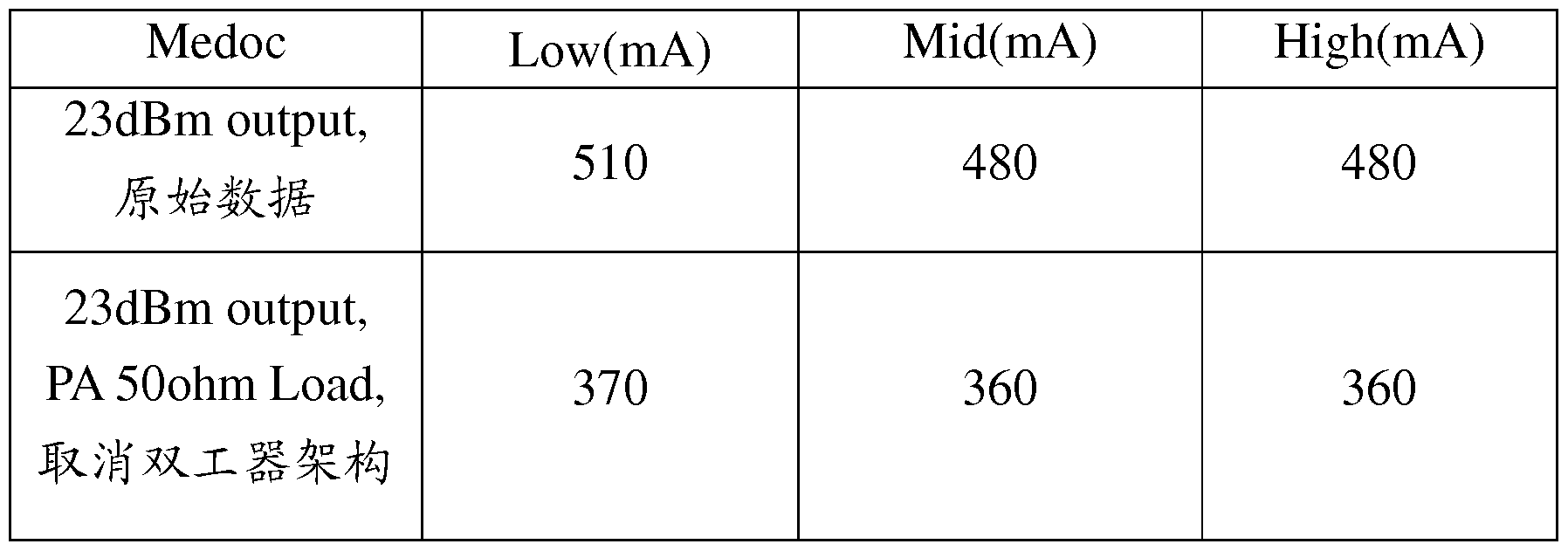
可以得出本发明提出的移动通讯终端的天线架构可以获得最大 140mA的电 流改善。
综上所述, 本发明所提供的技术方案通过设置第一天线和第二天线, 令第 一天线从外界接收高频段射频信号, 并令第二天线发射待发射高频段射频信号
和待发射低频段射频信号, 令第二天线接收低频段射频信号。 从而省略了高频 双工器, 解决因使用高频双工器而引起的插损问题, 从而改善了发射通路在接 收频段的噪声水平, 另更可降低系统的耗电和发热水平, 同时筒化射频架构, 可获得具有低成本、 更紧凑的空间, 本发明尤其适合于输出功率比较低的平台。
以上所述仅为本发明的实施例, 并非因此限制本发明的专利范围, 凡是利 用本发明说明书及附图内容所作的等效结构或等效流程变换, 或直接或间接运 用在其他相关的技术领域, 均同理包括在本发明的专利保护范围内。
Claims
1. 一种移动通讯终端, 其特征在于, 包括:
第一天线, 用于从外界接收高频段射频信号;
无线收发机, 从所述第一天线获取所述高频段射频信号, 并根据所述高频 段射频信号产生第一基带信号;
基带处理器, 从所述无线收发机获取所述第一基带信号并解调, 并进一步 产生第二基带信号和第三基带信号以传输至所述无线收发机;
所述无线收发机进一步将所述第二基带信号转换为待发射高频段射频信 号, 将所述第三基带信号转换为待发射低频段射频信号;
第二天线, 从所述无线收发机获取所述待发射高频段射频信号和所述待发 射低频段射频信号并发射出去;
其中, 所述第二天线进一步从外界接收低频段射频信号, 所述无线收发机 从所述第二天线获取所述低频段射频信号, 并根据所述低频段射频信号产生第 四基带信号, 所述基带处理器从所述无线收发机获取所述第四基带信号并解调; 高频段射频信号功率放大器, 设置在所述第二天线与所述无线收发机之间, 用于对所述无线收发机产生的所述待发射高频段射频信号进行功率放大处理; 低频段射频信号功率放大器, 设置在所述第二天线与所述无线收发机之间,
2. 根据权利要求 1所述的移动通讯终端, 其特征在于, 所述高频段射频信 号包括 BC1和 BC4信号, 所述低频段射频信号包括 GSM HB信号和 GSM LB 信号, 所述待发射高频段射频信号包括 BC1/BC4信号以及 BC2信号, 所述待发 射低频段射频信号包括待发射 GSM HB信号、 待发射 GSM LB信号以及待发射 BC5/BC8信号。
3. 根据权利要求 1所述的移动通讯终端, 其特征在于, 所述移动通讯终端 进一步包括:
高频段射频信号接收声表面波滤波器, 设置在所述第一天线和所述无线收 发机之间, 用于对所述第一天线所接收的高频段射频信号进行接收声表面波滤 波处理;
低频段射频信号接收声表面波滤波器, 设置在所述第二天线和所述无线收 发机之间, 用于对所述第二天线所接收的低频段射频信号进行接收声表面波滤 波处理。
4. 一种移动通讯终端, 其特征在于, 包括:
第一天线, 用于从外界接收高频段射频信号;
无线收发机, 从所述第一天线获取所述高频段射频信号, 并根据所述高频 段射频信号产生第一基带信号;
基带处理器, 从所述无线收发机获取所述第一基带信号并解调, 并进一步 产生第二基带信号和第三基带信号以传输至所述无线收发机;
所述无线收发机进一步将所述第二基带信号转换为待发射高频段射频信 号, 将所述第三基带信号转换为待发射低频段射频信号;
第二天线, 从所述无线收发机获取所述待发射高频段射频信号和所述待发 射低频段射频信号并发射出去;
其中, 所述第二天线进一步从外界接收低频段射频信号, 所述无线收发机 从所述第二天线获取所述低频段射频信号, 并根据所述低频段射频信号产生第 四基带信号, 所述基带处理器从所述无线收发机获取所述第四基带信号并解调。
5. 根据权利要求 4所述的移动通讯终端, 其特征在于, 所述高频段射频信 号包括 BC1和 BC4信号, 所述低频段射频信号包括 GSM ΗΒ信号和 GSM LB 信号, 所述待发射高频段射频信号包括 BC1/BC4信号以及 BC2信号, 所述待发 射低频段射频信号包括待发射 GSM ΗΒ信号、 待发射 GSM LB信号以及待发射 BC5/BC8信号。
6. 根据权利要求 4所述的移动通讯终端, 其特征在于, 所述移动通讯终端 进一步包括:
高频段射频信号接收声表面波滤波器, 设置在所述第一天线和所述无线收 发机之间, 用于对所述第一天线所接收的高频段射频信号进行接收声表面波滤 波处理;
低频段射频信号接收声表面波滤波器, 设置在所述第二天线和所述无线收 发机之间, 用于对所述第二天线所接收的低频段射频信号进行接收声表面波滤 波处理。
7. 根据权利要求 4所述的移动通讯终端, 其特征在于, 所述移动通讯终端 进一步包括:
高频段射频信号功率放大器, 设置在所述第二天线与所述无线收发机之间, 用于对所述无线收发机产生的所述待发射高频段射频信号进行功率放大处理。
8. 根据权利要求 4所述的移动通讯终端, 其特征在于, 所述移动通讯终端 进一步包括:
低频段射频信号功率放大器, 设置在所述第二天线与所述无线收发机之间,
9. 一种移动通讯终端, 其特征在于, 包括:
第一天线, 用于从外界接收高频段射频信号和低频段射频信号;
无线收发机, 从所述第一天线获取所述高频段射频信号, 并根据所述高频 段射频信号产生第一基带信号, 从所述第一天线获取所述低频段射频信号, 并 根据所述低频段射频信号产生第二基带信号;
基带处理器, 从所述无线收发机获取所述第一基带信号和所述第二基带信 号并解调, 并进一步产生第三基带信号和第四基带信号以传输至所述无线收发 机;
所述无线收发机进一步将所述第三基带信号转换为待发射高频段射频信 号, 将所述第四基带信号转换为待发射低频段射频信号;
第二天线, 从所述无线收发机获取所述待发射高频段射频信号并发射出去; 其中, 所述第一天线进一步从所述无线收发机获取所述待发射低频段射频 信号并发射出去。
10. 根据权利要求 9所述的移动通讯终端, 其特征在于, 所述高频段射频信 号包括 BC1/BC4信号,所述低频段射频信号包括 GSM 900/850信号、 GSM DCS 信号以及 BC5/BC8信号, 所述待发射高频段射频信号包括 BC1/BC4信号以及 BC2信号, 所述待发射低频段射频信号包括待发射 GSM HB信号、待发射 GSM LB信号以及待发射 BC5/BC8信号。
11. 根据权利要求 9所述的移动通讯终端, 其特征在于, 所述移动通讯终端 进一步包括:
高频段射频信号接收声表面波滤波器, 设置在所述第一天线和所述无线收 发机之间, 用于对所述第一天线所接收的高频段射频信号进行接收声表面波滤 波处理;
低频段射频信号接收声表面波滤波器, 设置在所述第一天线和所述无线收 发机之间, 用于对所述第一天线所接收的低频段射频信号进行接收声表面波滤 波处理。
12. 根据权利要求 9所述的移动通讯终端, 其特征在于, 所述移动通讯终端 进一步包括:
高频段射频信号功率放大器, 设置在所述第二天线与所述无线收发机之间, 用于对所述无线收发机产生的所述待发射高频段射频信号进行功率放大处理。
13. 根据权利要求 9所述的移动通讯终端, 其特征在于, 所述移动通讯终端 进一步包括: 低频段射频信号功率放大器, 设置在所述第一天线与所述无线收发机之间,
Priority Applications (2)
| Application Number | Priority Date | Filing Date | Title |
|---|---|---|---|
| US14/376,582 US20150043620A1 (en) | 2012-05-02 | 2013-03-06 | Mobile communication terminal |
| EP13784438.7A EP2846602A4 (en) | 2012-05-02 | 2013-03-06 | MOBILE COMMUNICATION TERMINAL |
Applications Claiming Priority (2)
| Application Number | Priority Date | Filing Date | Title |
|---|---|---|---|
| CN201210134523.6 | 2012-05-02 | ||
| CN201210134523.6A CN102684864B (zh) | 2012-05-02 | 2012-05-02 | 一种移动通讯终端 |
Publications (1)
| Publication Number | Publication Date |
|---|---|
| WO2013163906A1 true WO2013163906A1 (zh) | 2013-11-07 |
Family
ID=46816270
Family Applications (1)
| Application Number | Title | Priority Date | Filing Date |
|---|---|---|---|
| PCT/CN2013/072239 WO2013163906A1 (zh) | 2012-05-02 | 2013-03-06 | 一种移动通讯终端 |
Country Status (4)
| Country | Link |
|---|---|
| US (1) | US20150043620A1 (zh) |
| EP (1) | EP2846602A4 (zh) |
| CN (1) | CN102684864B (zh) |
| WO (1) | WO2013163906A1 (zh) |
Families Citing this family (9)
| Publication number | Priority date | Publication date | Assignee | Title |
|---|---|---|---|---|
| CN102684864B (zh) * | 2012-05-02 | 2017-04-19 | 惠州Tcl移动通信有限公司 | 一种移动通讯终端 |
| US9685907B2 (en) | 2015-06-30 | 2017-06-20 | Texas Instruments Incorporated | Variable gain power amplifiers |
| CN105429647B (zh) * | 2015-11-06 | 2018-08-31 | 联想(北京)有限公司 | 电子设备及其控制方法 |
| CN105721957A (zh) * | 2016-02-16 | 2016-06-29 | 广东欧珀移动通信有限公司 | 基于智能终端的对讲通话方法及智能终端 |
| CN107104685B (zh) | 2017-05-27 | 2020-11-13 | 惠州Tcl移动通信有限公司 | 一种扩展lte b41频段带宽的移动终端及其方法 |
| CN110931940A (zh) * | 2019-12-06 | 2020-03-27 | 惠州Tcl移动通信有限公司 | 一种天线结构和移动终端 |
| CN111314044B (zh) * | 2020-03-30 | 2024-04-16 | 广东宽普科技有限公司 | 一种具有高散热性能的全双工通信装置 |
| CN113300734A (zh) * | 2021-05-10 | 2021-08-24 | Tcl通讯(宁波)有限公司 | 射频天线装置、射频天线装置信号收发方法及移动终端 |
| CN117674883A (zh) * | 2022-09-01 | 2024-03-08 | 华为技术有限公司 | 一种电子设备及其天线系统和射频前端模块 |
Citations (3)
| Publication number | Priority date | Publication date | Assignee | Title |
|---|---|---|---|---|
| CN102332929A (zh) * | 2011-09-23 | 2012-01-25 | 中兴通讯股份有限公司 | 双模射频模块、双模射频发送、接收方法以及用户终端 |
| CN102404879A (zh) * | 2011-11-04 | 2012-04-04 | 惠州Tcl移动通信有限公司 | 一种移动通讯终端 |
| CN102684864A (zh) * | 2012-05-02 | 2012-09-19 | 惠州Tcl移动通信有限公司 | 一种移动通讯终端 |
Family Cites Families (17)
| Publication number | Priority date | Publication date | Assignee | Title |
|---|---|---|---|---|
| DE10052711A1 (de) * | 2000-10-24 | 2002-05-02 | Siemens Ag | Multiband-Endgerät |
| US6897825B2 (en) * | 2001-10-29 | 2005-05-24 | Samsung Electronics Co., Ltd. | Antenna apparatus for folder type mobile phone |
| US6751470B1 (en) * | 2002-04-08 | 2004-06-15 | Nokia Corporation | Versatile RF front-end multiband mobile terminals |
| EP1502364A4 (en) * | 2002-04-22 | 2010-03-31 | Ipr Licensing Inc | TRANSMITTER-RECEIVER RADIO WITH MULTIPLE INPUTS AND OUTPUTS |
| KR20040008750A (ko) * | 2002-07-19 | 2004-01-31 | 주식회사 현대시스콤 | 이동통신 시스템에서의 적응 섹터 기술을 이용한 셀 용량증대 장치 및 그 제어 방법 |
| JP2007180597A (ja) * | 2004-09-01 | 2007-07-12 | Nokia Corp | 中継器及び中継方法 |
| US7400862B2 (en) * | 2004-10-25 | 2008-07-15 | Skyworks Solutions, Inc. | Transmit-receive switch architecture providing pre-transmit isolation |
| US7526326B2 (en) * | 2005-05-13 | 2009-04-28 | Sony Ericsson Mobile Communications Ab | Handheld wireless communicators with reduced free-space, near-field emissions |
| US7489276B2 (en) * | 2005-06-27 | 2009-02-10 | Research In Motion Limited | Mobile wireless communications device comprising multi-frequency band antenna and related methods |
| JP4647486B2 (ja) * | 2005-12-27 | 2011-03-09 | 京セラ株式会社 | 送受信回路 |
| US20080108312A1 (en) * | 2006-11-06 | 2008-05-08 | Fujitsu Limited | Switchable transceiver for relay station |
| US8644197B2 (en) * | 2008-12-24 | 2014-02-04 | Hollinworth Fund, L.L.C. | RF front-end module and antenna systems |
| US8780959B2 (en) * | 2009-01-13 | 2014-07-15 | Intel Mobile Communications GmbH | Integrated transceiver loop back self test by amplitude modulation |
| WO2011085125A1 (en) * | 2010-01-06 | 2011-07-14 | Rfaxis, Inc. | Transmit-receive radio frequency front end integrated circuits for laptop computer applications |
| US20130237294A1 (en) * | 2012-03-09 | 2013-09-12 | Research In Motion Limited | Auxiliary Antenna Array Attachment for Wireless Devices |
| US9225382B2 (en) * | 2013-05-20 | 2015-12-29 | Rf Micro Devices, Inc. | Tunable filter front end architecture for non-contiguous carrier aggregation |
| US20150065064A1 (en) * | 2013-08-30 | 2015-03-05 | Qualcomm Incorporated | Active interference cancellation in analog domain |
-
2012
- 2012-05-02 CN CN201210134523.6A patent/CN102684864B/zh active Active
-
2013
- 2013-03-06 WO PCT/CN2013/072239 patent/WO2013163906A1/zh active Application Filing
- 2013-03-06 US US14/376,582 patent/US20150043620A1/en not_active Abandoned
- 2013-03-06 EP EP13784438.7A patent/EP2846602A4/en not_active Withdrawn
Patent Citations (3)
| Publication number | Priority date | Publication date | Assignee | Title |
|---|---|---|---|---|
| CN102332929A (zh) * | 2011-09-23 | 2012-01-25 | 中兴通讯股份有限公司 | 双模射频模块、双模射频发送、接收方法以及用户终端 |
| CN102404879A (zh) * | 2011-11-04 | 2012-04-04 | 惠州Tcl移动通信有限公司 | 一种移动通讯终端 |
| CN102684864A (zh) * | 2012-05-02 | 2012-09-19 | 惠州Tcl移动通信有限公司 | 一种移动通讯终端 |
Non-Patent Citations (1)
| Title |
|---|
| See also references of EP2846602A4 * |
Also Published As
| Publication number | Publication date |
|---|---|
| US20150043620A1 (en) | 2015-02-12 |
| EP2846602A4 (en) | 2016-05-04 |
| CN102684864A (zh) | 2012-09-19 |
| EP2846602A1 (en) | 2015-03-11 |
| CN102684864B (zh) | 2017-04-19 |
Similar Documents
| Publication | Publication Date | Title |
|---|---|---|
| US9172420B2 (en) | Mobile communication terminal | |
| WO2013163906A1 (zh) | 一种移动通讯终端 | |
| US9204488B2 (en) | Wireless communication transmitting and receiving system | |
| KR101763997B1 (ko) | 전송 무선 주파수 신호와 수신 무선 주파수 신호 간의 개선된 격리에 관한 시스템 및 방법 | |
| WO2015096466A1 (zh) | 提高射频链路收发性能的装置、终端、方法、存储介质 | |
| WO2013063938A1 (zh) | 功率放大模块、多模射频收发器、双工器和多模终端 | |
| WO2015131456A1 (zh) | 多模双通终端 | |
| KR20080083700A (ko) | 다대역 무선 모듈 | |
| TW201251418A (en) | Dual mode mobile communication terminal | |
| KR20160039437A (ko) | 트랜시버 및 그 트랜시버의 동작 방법 | |
| WO2018208967A2 (en) | Variable channelized bandwidth booster | |
| KR101715403B1 (ko) | 다중모드 무선모뎀 | |
| WO2013063937A1 (zh) | 双模射频收发装置、滤波装置和双模终端 | |
| WO2013063916A1 (zh) | 功率放大装置、多模射频收发装置和多模终端 | |
| WO2015176438A1 (zh) | 一种射频收发方法及系统 | |
| WO2008119284A1 (fr) | Application frontale radiofréquence partagée, station de base et procédé permettant de partager une application frontale radiofréquence | |
| CN110890913A (zh) | 中继器 | |
| JP2014520492A (ja) | 多入力多出力信号伝送方法及び多入力多出力信号伝送装置 | |
| US11483779B2 (en) | User equipment and communication method | |
| CN201113986Y (zh) | 一种防止终端频段间射频干扰的装置及手机 | |
| CN208904990U (zh) | 有gsm的蜂窝射频电路 | |
| US8649811B2 (en) | Embryo frequency leakage for personalized wireless communication system | |
| WO2015100665A1 (zh) | 降低干扰的方法、基带处理单元及基站 | |
| US20220006510A1 (en) | Pre-amplifier for a modem | |
| WO2010130080A1 (zh) | 一种共享射频接收单元的方法、装置及系统 |
Legal Events
| Date | Code | Title | Description |
|---|---|---|---|
| 121 | Ep: the epo has been informed by wipo that ep was designated in this application |
Ref document number: 13784438 Country of ref document: EP Kind code of ref document: A1 |
|
| WWE | Wipo information: entry into national phase |
Ref document number: 2013784438 Country of ref document: EP |
|
| WWE | Wipo information: entry into national phase |
Ref document number: 14376582 Country of ref document: US |
|
| NENP | Non-entry into the national phase |
Ref country code: DE |