WO2013145666A1 - Organic electroluminescent element - Google Patents
Organic electroluminescent element Download PDFInfo
- Publication number
- WO2013145666A1 WO2013145666A1 PCT/JP2013/001946 JP2013001946W WO2013145666A1 WO 2013145666 A1 WO2013145666 A1 WO 2013145666A1 JP 2013001946 W JP2013001946 W JP 2013001946W WO 2013145666 A1 WO2013145666 A1 WO 2013145666A1
- Authority
- WO
- WIPO (PCT)
- Prior art keywords
- group
- substituted
- unsubstituted
- carbon atoms
- layer
- Prior art date
Links
- 150000001875 compounds Chemical class 0.000 claims abstract description 76
- 125000004432 carbon atom Chemical group C* 0.000 claims description 151
- 238000005401 electroluminescence Methods 0.000 claims description 81
- 125000003118 aryl group Chemical group 0.000 claims description 80
- -1 Anomoto Chemical group 0.000 claims description 63
- 239000000463 material Substances 0.000 claims description 39
- 125000000217 alkyl group Chemical group 0.000 claims description 38
- 125000000623 heterocyclic group Chemical group 0.000 claims description 28
- 229910052751 metal Inorganic materials 0.000 claims description 26
- 239000002184 metal Substances 0.000 claims description 26
- 125000000753 cycloalkyl group Chemical group 0.000 claims description 23
- 125000005843 halogen group Chemical group 0.000 claims description 22
- 125000004435 hydrogen atom Chemical group [H]* 0.000 claims description 22
- 125000004093 cyano group Chemical group *C#N 0.000 claims description 20
- 125000003545 alkoxy group Chemical group 0.000 claims description 18
- 125000003277 amino group Chemical group 0.000 claims description 18
- 125000004104 aryloxy group Chemical group 0.000 claims description 18
- 229910052799 carbon Inorganic materials 0.000 claims description 16
- 125000003709 fluoroalkyl group Chemical group 0.000 claims description 15
- 125000003710 aryl alkyl group Chemical group 0.000 claims description 13
- 125000004453 alkoxycarbonyl group Chemical group 0.000 claims description 12
- 125000005110 aryl thio group Chemical group 0.000 claims description 12
- 150000001721 carbon Chemical class 0.000 claims description 11
- 125000004428 fluoroalkoxy group Chemical group 0.000 claims description 11
- 229910052761 rare earth metal Inorganic materials 0.000 claims description 11
- 125000006413 ring segment Chemical group 0.000 claims description 11
- 229910052783 alkali metal Inorganic materials 0.000 claims description 10
- 125000003178 carboxy group Chemical group [H]OC(*)=O 0.000 claims description 10
- 125000000449 nitro group Chemical group [O-][N+](*)=O 0.000 claims description 10
- 150000002910 rare earth metals Chemical class 0.000 claims description 10
- 229910052784 alkaline earth metal Inorganic materials 0.000 claims description 9
- 125000004076 pyridyl group Chemical group 0.000 claims description 9
- 125000005493 quinolyl group Chemical group 0.000 claims description 9
- 125000003808 silyl group Chemical group [H][Si]([H])([H])[*] 0.000 claims description 9
- DGEZNRSVGBDHLK-UHFFFAOYSA-N [1,10]phenanthroline Chemical group C1=CN=C2C3=NC=CC=C3C=CC2=C1 DGEZNRSVGBDHLK-UHFFFAOYSA-N 0.000 claims description 7
- 125000003342 alkenyl group Chemical group 0.000 claims description 7
- 125000002887 hydroxy group Chemical group [H]O* 0.000 claims description 7
- 150000001340 alkali metals Chemical class 0.000 claims description 6
- 150000001342 alkaline earth metals Chemical class 0.000 claims description 6
- 150000004696 coordination complex Chemical class 0.000 claims description 6
- 125000005647 linker group Chemical group 0.000 claims description 6
- 125000002102 aryl alkyloxo group Chemical group 0.000 claims description 5
- 150000002909 rare earth metal compounds Chemical class 0.000 claims description 5
- 150000002736 metal compounds Chemical class 0.000 claims description 4
- 150000001413 amino acids Chemical class 0.000 claims description 3
- 125000005415 substituted alkoxy group Chemical group 0.000 claims description 3
- 239000010410 layer Substances 0.000 description 257
- 230000005525 hole transport Effects 0.000 description 35
- 238000002347 injection Methods 0.000 description 33
- 239000007924 injection Substances 0.000 description 33
- 239000010408 film Substances 0.000 description 31
- 239000000758 substrate Substances 0.000 description 25
- 230000032258 transport Effects 0.000 description 25
- 238000000034 method Methods 0.000 description 18
- 125000001424 substituent group Chemical group 0.000 description 16
- 239000002019 doping agent Substances 0.000 description 15
- 0 B(C(CCC=N1)C1=C(*C/C=C/CC1)C1=C1)C1c1ccc(cc2)c3c1ccc1c3c2ccc1 Chemical compound B(C(CCC=N1)C1=C(*C/C=C/CC1)C1=C1)C1c1ccc(cc2)c3c1ccc1c3c2ccc1 0.000 description 14
- 238000007740 vapor deposition Methods 0.000 description 11
- 230000015572 biosynthetic process Effects 0.000 description 10
- 239000012044 organic layer Substances 0.000 description 10
- 125000001997 phenyl group Chemical group [H]C1=C([H])C([H])=C(*)C([H])=C1[H] 0.000 description 10
- JUJWROOIHBZHMG-UHFFFAOYSA-N Pyridine Chemical group C1=CC=NC=C1 JUJWROOIHBZHMG-UHFFFAOYSA-N 0.000 description 9
- YTPLMLYBLZKORZ-UHFFFAOYSA-N Thiophene Chemical compound C=1C=CSC=1 YTPLMLYBLZKORZ-UHFFFAOYSA-N 0.000 description 9
- 229910052731 fluorine Inorganic materials 0.000 description 9
- 125000001624 naphthyl group Chemical group 0.000 description 9
- 239000011521 glass Substances 0.000 description 8
- 239000004642 Polyimide Substances 0.000 description 7
- 125000006615 aromatic heterocyclic group Chemical group 0.000 description 7
- 230000000052 comparative effect Effects 0.000 description 7
- 239000003446 ligand Substances 0.000 description 7
- 229920001721 polyimide Polymers 0.000 description 7
- YLQBMQCUIZJEEH-UHFFFAOYSA-N Furan Chemical group C=1C=COC=1 YLQBMQCUIZJEEH-UHFFFAOYSA-N 0.000 description 6
- 150000004982 aromatic amines Chemical class 0.000 description 6
- XJHCXCQVJFPJIK-UHFFFAOYSA-M caesium fluoride Chemical compound [F-].[Cs+] XJHCXCQVJFPJIK-UHFFFAOYSA-M 0.000 description 6
- 238000000151 deposition Methods 0.000 description 6
- 125000001153 fluoro group Chemical group F* 0.000 description 6
- PQXKHYXIUOZZFA-UHFFFAOYSA-M lithium fluoride Chemical compound [Li+].[F-] PQXKHYXIUOZZFA-UHFFFAOYSA-M 0.000 description 6
- MCJGNVYPOGVAJF-UHFFFAOYSA-N quinolin-8-ol Chemical class C1=CN=C2C(O)=CC=CC2=C1 MCJGNVYPOGVAJF-UHFFFAOYSA-N 0.000 description 6
- 239000011734 sodium Substances 0.000 description 6
- 238000001771 vacuum deposition Methods 0.000 description 6
- OKTJSMMVPCPJKN-UHFFFAOYSA-N Carbon Chemical compound [C] OKTJSMMVPCPJKN-UHFFFAOYSA-N 0.000 description 5
- 229910045601 alloy Inorganic materials 0.000 description 5
- 239000000956 alloy Substances 0.000 description 5
- 125000002029 aromatic hydrocarbon group Chemical group 0.000 description 5
- QVQLCTNNEUAWMS-UHFFFAOYSA-N barium oxide Chemical compound [Ba]=O QVQLCTNNEUAWMS-UHFFFAOYSA-N 0.000 description 5
- 239000004020 conductor Substances 0.000 description 5
- 230000008021 deposition Effects 0.000 description 5
- 125000001072 heteroaryl group Chemical group 0.000 description 5
- 239000011777 magnesium Substances 0.000 description 5
- 150000002739 metals Chemical class 0.000 description 5
- 125000002524 organometallic group Chemical group 0.000 description 5
- BASFCYQUMIYNBI-UHFFFAOYSA-N platinum Chemical compound [Pt] BASFCYQUMIYNBI-UHFFFAOYSA-N 0.000 description 5
- 238000004528 spin coating Methods 0.000 description 5
- 229910052782 aluminium Inorganic materials 0.000 description 4
- XAGFODPZIPBFFR-UHFFFAOYSA-N aluminium Chemical compound [Al] XAGFODPZIPBFFR-UHFFFAOYSA-N 0.000 description 4
- 150000001491 aromatic compounds Chemical class 0.000 description 4
- 229910052788 barium Inorganic materials 0.000 description 4
- 239000011575 calcium Substances 0.000 description 4
- 230000007423 decrease Effects 0.000 description 4
- 239000007772 electrode material Substances 0.000 description 4
- 239000000203 mixture Substances 0.000 description 4
- 229960003540 oxyquinoline Drugs 0.000 description 4
- 125000003373 pyrazinyl group Chemical group 0.000 description 4
- 239000002356 single layer Substances 0.000 description 4
- 229910052708 sodium Inorganic materials 0.000 description 4
- PUZPDOWCWNUUKD-UHFFFAOYSA-M sodium fluoride Chemical compound [F-].[Na+] PUZPDOWCWNUUKD-UHFFFAOYSA-M 0.000 description 4
- 238000004544 sputter deposition Methods 0.000 description 4
- IATRAKWUXMZMIY-UHFFFAOYSA-N strontium oxide Chemical compound [O-2].[Sr+2] IATRAKWUXMZMIY-UHFFFAOYSA-N 0.000 description 4
- 238000000859 sublimation Methods 0.000 description 4
- 230000008022 sublimation Effects 0.000 description 4
- 229930192474 thiophene Natural products 0.000 description 4
- 239000005725 8-Hydroxyquinoline Substances 0.000 description 3
- ODINCKMPIJJUCX-UHFFFAOYSA-N Calcium oxide Chemical compound [Ca]=O ODINCKMPIJJUCX-UHFFFAOYSA-N 0.000 description 3
- PXGOKWXKJXAPGV-UHFFFAOYSA-N Fluorine Chemical compound FF PXGOKWXKJXAPGV-UHFFFAOYSA-N 0.000 description 3
- FYYHWMGAXLPEAU-UHFFFAOYSA-N Magnesium Chemical compound [Mg] FYYHWMGAXLPEAU-UHFFFAOYSA-N 0.000 description 3
- 229910001508 alkali metal halide Inorganic materials 0.000 description 3
- 150000008045 alkali metal halides Chemical class 0.000 description 3
- 229910001615 alkaline earth metal halide Inorganic materials 0.000 description 3
- 125000005428 anthryl group Chemical group [H]C1=C([H])C([H])=C2C([H])=C3C(*)=C([H])C([H])=C([H])C3=C([H])C2=C1[H] 0.000 description 3
- 150000004945 aromatic hydrocarbons Chemical group 0.000 description 3
- 125000004429 atom Chemical group 0.000 description 3
- DSAJWYNOEDNPEQ-UHFFFAOYSA-N barium atom Chemical compound [Ba] DSAJWYNOEDNPEQ-UHFFFAOYSA-N 0.000 description 3
- 229910052792 caesium Inorganic materials 0.000 description 3
- 239000013522 chelant Chemical class 0.000 description 3
- 125000002676 chrysenyl group Chemical group C1(=CC=CC=2C3=CC=C4C=CC=CC4=C3C=CC12)* 0.000 description 3
- 125000004122 cyclic group Chemical group 0.000 description 3
- 125000000113 cyclohexyl group Chemical group [H]C1([H])C([H])([H])C([H])([H])C([H])(*)C([H])([H])C1([H])[H] 0.000 description 3
- 230000000694 effects Effects 0.000 description 3
- 230000005684 electric field Effects 0.000 description 3
- 125000001495 ethyl group Chemical group [H]C([H])([H])C([H])([H])* 0.000 description 3
- 238000000605 extraction Methods 0.000 description 3
- 125000003983 fluorenyl group Chemical group C1(=CC=CC=2C3=CC=CC=C3CC12)* 0.000 description 3
- 239000011737 fluorine Substances 0.000 description 3
- 238000010438 heat treatment Methods 0.000 description 3
- RAXXELZNTBOGNW-UHFFFAOYSA-N imidazole Natural products C1=CNC=N1 RAXXELZNTBOGNW-UHFFFAOYSA-N 0.000 description 3
- 150000002484 inorganic compounds Chemical class 0.000 description 3
- 229910010272 inorganic material Inorganic materials 0.000 description 3
- 229910052744 lithium Inorganic materials 0.000 description 3
- 125000002496 methyl group Chemical group [H]C([H])([H])* 0.000 description 3
- 229910052757 nitrogen Inorganic materials 0.000 description 3
- 125000004433 nitrogen atom Chemical group N* 0.000 description 3
- 150000002894 organic compounds Chemical class 0.000 description 3
- 150000004866 oxadiazoles Chemical class 0.000 description 3
- 229910052697 platinum Inorganic materials 0.000 description 3
- 230000008569 process Effects 0.000 description 3
- 125000001725 pyrenyl group Chemical group 0.000 description 3
- 229910052712 strontium Inorganic materials 0.000 description 3
- 238000003786 synthesis reaction Methods 0.000 description 3
- 239000010409 thin film Substances 0.000 description 3
- 238000002834 transmittance Methods 0.000 description 3
- TVIVIEFSHFOWTE-UHFFFAOYSA-K tri(quinolin-8-yloxy)alumane Chemical compound [Al+3].C1=CN=C2C([O-])=CC=CC2=C1.C1=CN=C2C([O-])=CC=CC2=C1.C1=CN=C2C([O-])=CC=CC2=C1 TVIVIEFSHFOWTE-UHFFFAOYSA-K 0.000 description 3
- VERMWGQSKPXSPZ-BUHFOSPRSA-N 1-[(e)-2-phenylethenyl]anthracene Chemical class C=1C=CC2=CC3=CC=CC=C3C=C2C=1\C=C\C1=CC=CC=C1 VERMWGQSKPXSPZ-BUHFOSPRSA-N 0.000 description 2
- HYZJCKYKOHLVJF-UHFFFAOYSA-N 1H-benzimidazole Chemical compound C1=CC=C2NC=NC2=C1 HYZJCKYKOHLVJF-UHFFFAOYSA-N 0.000 description 2
- IXHWGNYCZPISET-UHFFFAOYSA-N 2-[4-(dicyanomethylidene)-2,3,5,6-tetrafluorocyclohexa-2,5-dien-1-ylidene]propanedinitrile Chemical compound FC1=C(F)C(=C(C#N)C#N)C(F)=C(F)C1=C(C#N)C#N IXHWGNYCZPISET-UHFFFAOYSA-N 0.000 description 2
- LTPBRCUWZOMYOC-UHFFFAOYSA-N Beryllium oxide Chemical compound O=[Be] LTPBRCUWZOMYOC-UHFFFAOYSA-N 0.000 description 2
- WKBOTKDWSSQWDR-UHFFFAOYSA-N Bromine atom Chemical group [Br] WKBOTKDWSSQWDR-UHFFFAOYSA-N 0.000 description 2
- DGAQECJNVWCQMB-PUAWFVPOSA-M Ilexoside XXIX Chemical compound C[C@@H]1CC[C@@]2(CC[C@@]3(C(=CC[C@H]4[C@]3(CC[C@@H]5[C@@]4(CC[C@@H](C5(C)C)OS(=O)(=O)[O-])C)C)[C@@H]2[C@]1(C)O)C)C(=O)O[C@H]6[C@@H]([C@H]([C@@H]([C@H](O6)CO)O)O)O.[Na+] DGAQECJNVWCQMB-PUAWFVPOSA-M 0.000 description 2
- 229910000733 Li alloy Inorganic materials 0.000 description 2
- WHXSMMKQMYFTQS-UHFFFAOYSA-N Lithium Chemical compound [Li] WHXSMMKQMYFTQS-UHFFFAOYSA-N 0.000 description 2
- 229910000861 Mg alloy Inorganic materials 0.000 description 2
- PAYRUJLWNCNPSJ-UHFFFAOYSA-N N-phenyl amine Natural products NC1=CC=CC=C1 PAYRUJLWNCNPSJ-UHFFFAOYSA-N 0.000 description 2
- PXHVJJICTQNCMI-UHFFFAOYSA-N Nickel Chemical compound [Ni] PXHVJJICTQNCMI-UHFFFAOYSA-N 0.000 description 2
- WCUXLLCKKVVCTQ-UHFFFAOYSA-M Potassium chloride Chemical compound [Cl-].[K+] WCUXLLCKKVVCTQ-UHFFFAOYSA-M 0.000 description 2
- KYQCOXFCLRTKLS-UHFFFAOYSA-N Pyrazine Chemical compound C1=CN=CC=N1 KYQCOXFCLRTKLS-UHFFFAOYSA-N 0.000 description 2
- BQCADISMDOOEFD-UHFFFAOYSA-N Silver Chemical compound [Ag] BQCADISMDOOEFD-UHFFFAOYSA-N 0.000 description 2
- FAPWRFPIFSIZLT-UHFFFAOYSA-M Sodium chloride Chemical compound [Na+].[Cl-] FAPWRFPIFSIZLT-UHFFFAOYSA-M 0.000 description 2
- 229910052769 Ytterbium Inorganic materials 0.000 description 2
- 150000001339 alkali metal compounds Chemical class 0.000 description 2
- 150000001341 alkaline earth metal compounds Chemical class 0.000 description 2
- 125000002947 alkylene group Chemical group 0.000 description 2
- MWPLVEDNUUSJAV-UHFFFAOYSA-N anthracene Chemical compound C1=CC=CC2=CC3=CC=CC=C3C=C21 MWPLVEDNUUSJAV-UHFFFAOYSA-N 0.000 description 2
- 125000005577 anthracene group Chemical group 0.000 description 2
- IOJUPLGTWVMSFF-UHFFFAOYSA-N benzothiazole Chemical compound C1=CC=C2SC=NC2=C1 IOJUPLGTWVMSFF-UHFFFAOYSA-N 0.000 description 2
- 239000005388 borosilicate glass Substances 0.000 description 2
- 125000000484 butyl group Chemical group [H]C([*])([H])C([H])([H])C([H])([H])C([H])([H])[H] 0.000 description 2
- 229910052791 calcium Inorganic materials 0.000 description 2
- BRPQOXSCLDDYGP-UHFFFAOYSA-N calcium oxide Chemical compound [O-2].[Ca+2] BRPQOXSCLDDYGP-UHFFFAOYSA-N 0.000 description 2
- 239000000292 calcium oxide Substances 0.000 description 2
- 229910052801 chlorine Inorganic materials 0.000 description 2
- 125000001309 chloro group Chemical group Cl* 0.000 description 2
- 239000003086 colorant Substances 0.000 description 2
- 229920001940 conductive polymer Polymers 0.000 description 2
- 229920001577 copolymer Polymers 0.000 description 2
- 238000002425 crystallisation Methods 0.000 description 2
- 230000008025 crystallization Effects 0.000 description 2
- ZSWFCLXCOIISFI-UHFFFAOYSA-N cyclopentadiene Chemical compound C1C=CC=C1 ZSWFCLXCOIISFI-UHFFFAOYSA-N 0.000 description 2
- 125000001511 cyclopentyl group Chemical group [H]C1([H])C([H])([H])C([H])([H])C([H])(*)C1([H])[H] 0.000 description 2
- 239000000412 dendrimer Substances 0.000 description 2
- 229920000736 dendritic polymer Polymers 0.000 description 2
- 238000010586 diagram Methods 0.000 description 2
- XUCJHNOBJLKZNU-UHFFFAOYSA-M dilithium;hydroxide Chemical compound [Li+].[Li+].[OH-] XUCJHNOBJLKZNU-UHFFFAOYSA-M 0.000 description 2
- GVEPBJHOBDJJJI-UHFFFAOYSA-N fluoranthrene Natural products C1=CC(C2=CC=CC=C22)=C3C2=CC=CC3=C1 GVEPBJHOBDJJJI-UHFFFAOYSA-N 0.000 description 2
- 150000008376 fluorenones Chemical class 0.000 description 2
- 150000002222 fluorine compounds Chemical class 0.000 description 2
- 150000004820 halides Chemical class 0.000 description 2
- 229940083761 high-ceiling diuretics pyrazolone derivative Drugs 0.000 description 2
- 150000007857 hydrazones Chemical class 0.000 description 2
- 150000002430 hydrocarbons Chemical group 0.000 description 2
- 229910052739 hydrogen Inorganic materials 0.000 description 2
- 239000001257 hydrogen Substances 0.000 description 2
- 150000002460 imidazoles Chemical class 0.000 description 2
- 229910052738 indium Inorganic materials 0.000 description 2
- 239000011810 insulating material Substances 0.000 description 2
- 239000012212 insulator Substances 0.000 description 2
- 229940079865 intestinal antiinfectives imidazole derivative Drugs 0.000 description 2
- 125000001449 isopropyl group Chemical group [H]C([H])([H])C([H])(*)C([H])([H])[H] 0.000 description 2
- 238000010030 laminating Methods 0.000 description 2
- KWGKDLIKAYFUFQ-UHFFFAOYSA-M lithium chloride Chemical compound [Li+].[Cl-] KWGKDLIKAYFUFQ-UHFFFAOYSA-M 0.000 description 2
- 229910052749 magnesium Inorganic materials 0.000 description 2
- 238000004519 manufacturing process Methods 0.000 description 2
- 229910044991 metal oxide Inorganic materials 0.000 description 2
- 150000004706 metal oxides Chemical class 0.000 description 2
- 238000002156 mixing Methods 0.000 description 2
- IBHBKWKFFTZAHE-UHFFFAOYSA-N n-[4-[4-(n-naphthalen-1-ylanilino)phenyl]phenyl]-n-phenylnaphthalen-1-amine Chemical compound C1=CC=CC=C1N(C=1C2=CC=CC=C2C=CC=1)C1=CC=C(C=2C=CC(=CC=2)N(C=2C=CC=CC=2)C=2C3=CC=CC=C3C=CC=2)C=C1 IBHBKWKFFTZAHE-UHFFFAOYSA-N 0.000 description 2
- 239000011368 organic material Substances 0.000 description 2
- 150000007978 oxazole derivatives Chemical class 0.000 description 2
- 239000002245 particle Substances 0.000 description 2
- 125000005561 phenanthryl group Chemical group 0.000 description 2
- 150000004986 phenylenediamines Chemical class 0.000 description 2
- IEQIEDJGQAUEQZ-UHFFFAOYSA-N phthalocyanine Chemical compound N1C(N=C2C3=CC=CC=C3C(N=C3C4=CC=CC=C4C(=N4)N3)=N2)=C(C=CC=C2)C2=C1N=C1C2=CC=CC=C2C4=N1 IEQIEDJGQAUEQZ-UHFFFAOYSA-N 0.000 description 2
- 229920000548 poly(silane) polymer Polymers 0.000 description 2
- 229920000642 polymer Polymers 0.000 description 2
- 229920000123 polythiophene Polymers 0.000 description 2
- 150000004032 porphyrins Chemical class 0.000 description 2
- 229910052700 potassium Inorganic materials 0.000 description 2
- 125000001436 propyl group Chemical group [H]C([*])([H])C([H])([H])C([H])([H])[H] 0.000 description 2
- JEXVQSWXXUJEMA-UHFFFAOYSA-N pyrazol-3-one Chemical class O=C1C=CN=N1 JEXVQSWXXUJEMA-UHFFFAOYSA-N 0.000 description 2
- 150000003219 pyrazolines Chemical class 0.000 description 2
- BBEAQIROQSPTKN-UHFFFAOYSA-N pyrene Chemical compound C1=CC=C2C=CC3=CC=CC4=CC=C1C2=C43 BBEAQIROQSPTKN-UHFFFAOYSA-N 0.000 description 2
- UMJSCPRVCHMLSP-UHFFFAOYSA-N pyridine Natural products COC1=CC=CN=C1 UMJSCPRVCHMLSP-UHFFFAOYSA-N 0.000 description 2
- 229910052702 rhenium Inorganic materials 0.000 description 2
- 229910052701 rubidium Inorganic materials 0.000 description 2
- 229920006395 saturated elastomer Polymers 0.000 description 2
- 239000004065 semiconductor Substances 0.000 description 2
- 229910052710 silicon Inorganic materials 0.000 description 2
- 229910052709 silver Inorganic materials 0.000 description 2
- 239000004332 silver Substances 0.000 description 2
- PJANXHGTPQOBST-UHFFFAOYSA-N stilbene Chemical class C=1C=CC=CC=1C=CC1=CC=CC=C1 PJANXHGTPQOBST-UHFFFAOYSA-N 0.000 description 2
- CIOAGBVUUVVLOB-UHFFFAOYSA-N strontium atom Chemical compound [Sr] CIOAGBVUUVVLOB-UHFFFAOYSA-N 0.000 description 2
- 239000000126 substance Substances 0.000 description 2
- 229940042055 systemic antimycotics triazole derivative Drugs 0.000 description 2
- 125000000999 tert-butyl group Chemical group [H]C([H])([H])C(*)(C([H])([H])[H])C([H])([H])[H] 0.000 description 2
- 125000004665 trialkylsilyl group Chemical group 0.000 description 2
- 125000002023 trifluoromethyl group Chemical group FC(F)(F)* 0.000 description 2
- 125000000026 trimethylsilyl group Chemical group [H]C([H])([H])[Si]([*])(C([H])([H])[H])C([H])([H])[H] 0.000 description 2
- 238000007738 vacuum evaporation Methods 0.000 description 2
- UWRZIZXBOLBCON-VOTSOKGWSA-N (e)-2-phenylethenamine Chemical class N\C=C\C1=CC=CC=C1 UWRZIZXBOLBCON-VOTSOKGWSA-N 0.000 description 1
- POILWHVDKZOXJZ-ARJAWSKDSA-M (z)-4-oxopent-2-en-2-olate Chemical compound C\C([O-])=C\C(C)=O POILWHVDKZOXJZ-ARJAWSKDSA-M 0.000 description 1
- JYEUMXHLPRZUAT-UHFFFAOYSA-N 1,2,3-triazine Chemical compound C1=CN=NN=C1 JYEUMXHLPRZUAT-UHFFFAOYSA-N 0.000 description 1
- BCMCBBGGLRIHSE-UHFFFAOYSA-N 1,3-benzoxazole Chemical compound C1=CC=C2OC=NC2=C1 BCMCBBGGLRIHSE-UHFFFAOYSA-N 0.000 description 1
- KLCLIOISYBHYDZ-UHFFFAOYSA-N 1,4,4-triphenylbuta-1,3-dienylbenzene Chemical class C=1C=CC=CC=1C(C=1C=CC=CC=1)=CC=C(C=1C=CC=CC=1)C1=CC=CC=C1 KLCLIOISYBHYDZ-UHFFFAOYSA-N 0.000 description 1
- FLBAYUMRQUHISI-UHFFFAOYSA-N 1,8-naphthyridine Chemical group N1=CC=CC2=CC=CN=C21 FLBAYUMRQUHISI-UHFFFAOYSA-N 0.000 description 1
- IANQTJSKSUMEQM-UHFFFAOYSA-N 1-benzofuran Chemical group C1=CC=C2OC=CC2=C1 IANQTJSKSUMEQM-UHFFFAOYSA-N 0.000 description 1
- FCEHBMOGCRZNNI-UHFFFAOYSA-N 1-benzothiophene Chemical group C1=CC=C2SC=CC2=C1 FCEHBMOGCRZNNI-UHFFFAOYSA-N 0.000 description 1
- 125000001637 1-naphthyl group Chemical group [H]C1=C([H])C([H])=C2C(*)=C([H])C([H])=C([H])C2=C1[H] 0.000 description 1
- UIWLITBBFICQKW-UHFFFAOYSA-N 1h-benzo[h]quinolin-2-one Chemical compound C1=CC=C2C3=NC(O)=CC=C3C=CC2=C1 UIWLITBBFICQKW-UHFFFAOYSA-N 0.000 description 1
- 125000004793 2,2,2-trifluoroethoxy group Chemical group FC(CO*)(F)F 0.000 description 1
- SULWTXOWAFVWOY-PHEQNACWSA-N 2,3-bis[(E)-2-phenylethenyl]pyrazine Chemical class C=1C=CC=CC=1/C=C/C1=NC=CN=C1\C=C\C1=CC=CC=C1 SULWTXOWAFVWOY-PHEQNACWSA-N 0.000 description 1
- MVWPVABZQQJTPL-UHFFFAOYSA-N 2,3-diphenylcyclohexa-2,5-diene-1,4-dione Chemical class O=C1C=CC(=O)C(C=2C=CC=CC=2)=C1C1=CC=CC=C1 MVWPVABZQQJTPL-UHFFFAOYSA-N 0.000 description 1
- NSMJMUQZRGZMQC-UHFFFAOYSA-N 2-naphthalen-1-yl-1H-imidazo[4,5-f][1,10]phenanthroline Chemical compound C12=CC=CN=C2C2=NC=CC=C2C2=C1NC(C=1C3=CC=CC=C3C=CC=1)=N2 NSMJMUQZRGZMQC-UHFFFAOYSA-N 0.000 description 1
- VLRSADZEDXVUPG-UHFFFAOYSA-N 2-naphthalen-1-ylpyridine Chemical class N1=CC=CC=C1C1=CC=CC2=CC=CC=C12 VLRSADZEDXVUPG-UHFFFAOYSA-N 0.000 description 1
- 125000001622 2-naphthyl group Chemical group [H]C1=C([H])C([H])=C2C([H])=C(*)C([H])=C([H])C2=C1[H] 0.000 description 1
- 125000005979 2-naphthyloxy group Chemical group 0.000 description 1
- FZTBAQBBLSYHJZ-UHFFFAOYSA-N 2-phenyl-1,3-oxazol-4-ol Chemical compound OC1=COC(C=2C=CC=CC=2)=N1 FZTBAQBBLSYHJZ-UHFFFAOYSA-N 0.000 description 1
- CCMLIFHRMDXEBM-UHFFFAOYSA-N 2-phenyl-1,3-thiazol-4-ol Chemical compound OC1=CSC(C=2C=CC=CC=2)=N1 CCMLIFHRMDXEBM-UHFFFAOYSA-N 0.000 description 1
- HJJXCBIOYBUVBH-UHFFFAOYSA-N 2-phenyl-1h-benzimidazol-4-ol Chemical compound N1C=2C(O)=CC=CC=2N=C1C1=CC=CC=C1 HJJXCBIOYBUVBH-UHFFFAOYSA-N 0.000 description 1
- VHRHRMPFHJXSNR-UHFFFAOYSA-N 2-phenylpyridin-3-ol Chemical compound OC1=CC=CN=C1C1=CC=CC=C1 VHRHRMPFHJXSNR-UHFFFAOYSA-N 0.000 description 1
- 150000005360 2-phenylpyridines Chemical class 0.000 description 1
- FSEXLNMNADBYJU-UHFFFAOYSA-N 2-phenylquinoline Chemical class C1=CC=CC=C1C1=CC=C(C=CC=C2)C2=N1 FSEXLNMNADBYJU-UHFFFAOYSA-N 0.000 description 1
- QLPKTAFPRRIFQX-UHFFFAOYSA-N 2-thiophen-2-ylpyridine Chemical class C1=CSC(C=2N=CC=CC=2)=C1 QLPKTAFPRRIFQX-UHFFFAOYSA-N 0.000 description 1
- JMTMSDXUXJISAY-UHFFFAOYSA-N 2H-benzotriazol-4-ol Chemical compound OC1=CC=CC2=C1N=NN2 JMTMSDXUXJISAY-UHFFFAOYSA-N 0.000 description 1
- DMEVMYSQZPJFOK-UHFFFAOYSA-N 3,4,5,6,9,10-hexazatetracyclo[12.4.0.02,7.08,13]octadeca-1(18),2(7),3,5,8(13),9,11,14,16-nonaene Chemical group N1=NN=C2C3=CC=CC=C3C3=CC=NN=C3C2=N1 DMEVMYSQZPJFOK-UHFFFAOYSA-N 0.000 description 1
- DHDHJYNTEFLIHY-UHFFFAOYSA-N 4,7-diphenyl-1,10-phenanthroline Chemical compound C1=CC=CC=C1C1=CC=NC2=C1C=CC1=C(C=3C=CC=CC=3)C=CN=C21 DHDHJYNTEFLIHY-UHFFFAOYSA-N 0.000 description 1
- CMSGUKVDXXTJDQ-UHFFFAOYSA-N 4-(2-naphthalen-1-ylethylamino)-4-oxobutanoic acid Chemical compound C1=CC=C2C(CCNC(=O)CCC(=O)O)=CC=CC2=C1 CMSGUKVDXXTJDQ-UHFFFAOYSA-N 0.000 description 1
- GAMYYCRTACQSBR-UHFFFAOYSA-N 4-azabenzimidazole Chemical compound C1=CC=C2NC=NC2=N1 GAMYYCRTACQSBR-UHFFFAOYSA-N 0.000 description 1
- ZCYVEMRRCGMTRW-UHFFFAOYSA-N 7553-56-2 Chemical group [I] ZCYVEMRRCGMTRW-UHFFFAOYSA-N 0.000 description 1
- ZHQNDEHZACHHTA-UHFFFAOYSA-N 9,9-dimethylfluorene Chemical group C1=CC=C2C(C)(C)C3=CC=CC=C3C2=C1 ZHQNDEHZACHHTA-UHFFFAOYSA-N 0.000 description 1
- RXACYPFGPNTUNV-UHFFFAOYSA-N 9,9-dioctylfluorene Chemical group C1=CC=C2C(CCCCCCCC)(CCCCCCCC)C3=CC=CC=C3C2=C1 RXACYPFGPNTUNV-UHFFFAOYSA-N 0.000 description 1
- ZYASLTYCYTYKFC-UHFFFAOYSA-N 9-methylidenefluorene Chemical class C1=CC=C2C(=C)C3=CC=CC=C3C2=C1 ZYASLTYCYTYKFC-UHFFFAOYSA-N 0.000 description 1
- 229910001316 Ag alloy Inorganic materials 0.000 description 1
- 229910000838 Al alloy Inorganic materials 0.000 description 1
- 229910016036 BaF 2 Inorganic materials 0.000 description 1
- ROFVEXUMMXZLPA-UHFFFAOYSA-N Bipyridyl Chemical group N1=CC=CC=C1C1=CC=CC=N1 ROFVEXUMMXZLPA-UHFFFAOYSA-N 0.000 description 1
- JCAAOOLSJBOELT-UHFFFAOYSA-N C(C12)C=CN=C1c1ncccc1C(c(cc1)cc3c1c1ccccc1c1ccccc31)=C2c1cc2c(cccc3)c3c(cccc3)c3c2cc1 Chemical compound C(C12)C=CN=C1c1ncccc1C(c(cc1)cc3c1c1ccccc1c1ccccc31)=C2c1cc2c(cccc3)c3c(cccc3)c3c2cc1 JCAAOOLSJBOELT-UHFFFAOYSA-N 0.000 description 1
- GSQVDQRKDQPDBY-LMCGJEQXSA-N COc(cc1)cc(-c(c2c3)cc4c3-c3cc(OC)ccc3/C4=N\C#N)c1/C2=N\C#N Chemical compound COc(cc1)cc(-c(c2c3)cc4c3-c3cc(OC)ccc3/C4=N\C#N)c1/C2=N\C#N GSQVDQRKDQPDBY-LMCGJEQXSA-N 0.000 description 1
- GEPSWDHBXGSIGF-UHFFFAOYSA-N COc(cc1C(C2C=C3c4cc(OC)ccc44)C=C3C4=C(C#N)C#N)ccc1C2=C(C#N)C#N Chemical compound COc(cc1C(C2C=C3c4cc(OC)ccc44)C=C3C4=C(C#N)C#N)ccc1C2=C(C#N)C#N GEPSWDHBXGSIGF-UHFFFAOYSA-N 0.000 description 1
- 229910004261 CaF 2 Inorganic materials 0.000 description 1
- OYPRJOBELJOOCE-UHFFFAOYSA-N Calcium Chemical compound [Ca] OYPRJOBELJOOCE-UHFFFAOYSA-N 0.000 description 1
- AJPAYWQVIQAEDZ-UHFFFAOYSA-N Cc1c(-c2ccc(C(F)(F)F)cc2C2=C(C#N)C#N)c2c(C)c(-c2ccc(C(F)(F)F)cc22)c1C2=C(C#N)C#N Chemical compound Cc1c(-c2ccc(C(F)(F)F)cc2C2=C(C#N)C#N)c2c(C)c(-c2ccc(C(F)(F)F)cc22)c1C2=C(C#N)C#N AJPAYWQVIQAEDZ-UHFFFAOYSA-N 0.000 description 1
- 229910052684 Cerium Inorganic materials 0.000 description 1
- VYZAMTAEIAYCRO-UHFFFAOYSA-N Chromium Chemical compound [Cr] VYZAMTAEIAYCRO-UHFFFAOYSA-N 0.000 description 1
- RYGMFSIKBFXOCR-UHFFFAOYSA-N Copper Chemical compound [Cu] RYGMFSIKBFXOCR-UHFFFAOYSA-N 0.000 description 1
- YZCKVEUIGOORGS-OUBTZVSYSA-N Deuterium Chemical compound [2H] YZCKVEUIGOORGS-OUBTZVSYSA-N 0.000 description 1
- KRHYYFGTRYWZRS-UHFFFAOYSA-N Fluorane Chemical compound F KRHYYFGTRYWZRS-UHFFFAOYSA-N 0.000 description 1
- 229910000799 K alloy Inorganic materials 0.000 description 1
- 229910018068 Li 2 O Inorganic materials 0.000 description 1
- ZOKXTWBITQBERF-UHFFFAOYSA-N Molybdenum Chemical compound [Mo] ZOKXTWBITQBERF-UHFFFAOYSA-N 0.000 description 1
- YFBNEWJCEUJHNU-NCOOAAOESA-N N#C/N=C(/c1c2)\c(cc(cc3)Oc4ccc(C(F)(F)F)cc4)c3-c1cc1c2-c(ccc(Oc2ccc(C(F)(F)F)cc2)c2)c2/C1=N\C#N Chemical compound N#C/N=C(/c1c2)\c(cc(cc3)Oc4ccc(C(F)(F)F)cc4)c3-c1cc1c2-c(ccc(Oc2ccc(C(F)(F)F)cc2)c2)c2/C1=N\C#N YFBNEWJCEUJHNU-NCOOAAOESA-N 0.000 description 1
- YWTRGZWWXMUZJJ-OSIAYSHKSA-N N#C/N=C(/c1cc(-c(c2c3)ccc3-c3cc(C(F)(F)F)ccc3)c3/C2=N/C#N)\c2cc(-c4cc(C(F)(F)F)ccc4)ccc2-c1c3-c1ccccc1 Chemical compound N#C/N=C(/c1cc(-c(c2c3)ccc3-c3cc(C(F)(F)F)ccc3)c3/C2=N/C#N)\c2cc(-c4cc(C(F)(F)F)ccc4)ccc2-c1c3-c1ccccc1 YWTRGZWWXMUZJJ-OSIAYSHKSA-N 0.000 description 1
- HJZOIEBJZKZDJY-NCOOAAOESA-N N#C/N=C(\c1c-2ccc(C(F)(F)F)c1)/c(c(-c1ccccc1)c1-c3ccc(C(F)(F)F)cc33)c-2c(-c2ccccc2)c1/C3=N/C#N Chemical compound N#C/N=C(\c1c-2ccc(C(F)(F)F)c1)/c(c(-c1ccccc1)c1-c3ccc(C(F)(F)F)cc33)c-2c(-c2ccccc2)c1/C3=N/C#N HJZOIEBJZKZDJY-NCOOAAOESA-N 0.000 description 1
- ROHSCEWMSWUGAQ-CFTRLRGZSA-N N#C/N=C(\c1cc(F)ccc1-c1c(c(/C(/c2c3)=N/C#N)c4-c2ccc3F)-c2ccccc2)/c1c4-c1ccccc1 Chemical compound N#C/N=C(\c1cc(F)ccc1-c1c(c(/C(/c2c3)=N/C#N)c4-c2ccc3F)-c2ccccc2)/c1c4-c1ccccc1 ROHSCEWMSWUGAQ-CFTRLRGZSA-N 0.000 description 1
- XCWSXAMZSIHFBV-YEQLPCBTSA-N N#C/N=C(\c1ccccc1-1)/c(c(-c2ccccc2)c2-c3ccccc33)c-1c(-c1ccccc1)c2/C3=N/C#N Chemical compound N#C/N=C(\c1ccccc1-1)/c(c(-c2ccccc2)c2-c3ccccc33)c-1c(-c1ccccc1)c2/C3=N/C#N XCWSXAMZSIHFBV-YEQLPCBTSA-N 0.000 description 1
- VFQRMLBGPSCOBG-NCOOAAOESA-N N#C/N=C(\c1ccccc1-c1c(c2c3-c(cccc4)c4/C2=N\C#N)-c2ccc(C(F)(F)F)cc2)/c1c3-c1ccc(C(F)(F)F)cc1 Chemical compound N#C/N=C(\c1ccccc1-c1c(c2c3-c(cccc4)c4/C2=N\C#N)-c2ccc(C(F)(F)F)cc2)/c1c3-c1ccc(C(F)(F)F)cc1 VFQRMLBGPSCOBG-NCOOAAOESA-N 0.000 description 1
- BOLROAJDGPRIFH-JEVCVBCSSA-N N#C/N=C1/c2c(C(F)(F)F)c(-c3ccccc3/C3=N\C#N)c3c(-c3ccccc3)c2-c2c1cccc2 Chemical compound N#C/N=C1/c2c(C(F)(F)F)c(-c3ccccc3/C3=N\C#N)c3c(-c3ccccc3)c2-c2c1cccc2 BOLROAJDGPRIFH-JEVCVBCSSA-N 0.000 description 1
- BVWLKMPMEKWWDF-UHFFFAOYSA-N N#CC(C#N)=C(c1c2)c(cc(cc3)Oc4ccc(C(F)(F)F)cc4)c3-c1cc1c2-c(ccc(Oc2ccc(C(F)(F)F)cc2)c2)c2C1=C(C#N)C#N Chemical compound N#CC(C#N)=C(c1c2)c(cc(cc3)Oc4ccc(C(F)(F)F)cc4)c3-c1cc1c2-c(ccc(Oc2ccc(C(F)(F)F)cc2)c2)c2C1=C(C#N)C#N BVWLKMPMEKWWDF-UHFFFAOYSA-N 0.000 description 1
- WXZDMFMKIDWQCZ-UHFFFAOYSA-N N#CC(C#N)=C(c1cc(C(F)(F)F)ccc1-c1c(c2c3-c4ccc(C(F)(F)F)cc4C2=C(C#N)C#N)F)c1c3F Chemical compound N#CC(C#N)=C(c1cc(C(F)(F)F)ccc1-c1c(c2c3-c4ccc(C(F)(F)F)cc4C2=C(C#N)C#N)F)c1c3F WXZDMFMKIDWQCZ-UHFFFAOYSA-N 0.000 description 1
- ZCQWOFVYLHDMMC-UHFFFAOYSA-N Oxazole Chemical compound C1=COC=N1 ZCQWOFVYLHDMMC-UHFFFAOYSA-N 0.000 description 1
- PCNDJXKNXGMECE-UHFFFAOYSA-N Phenazine Natural products C1=CC=CC2=NC3=CC=CC=C3N=C21 PCNDJXKNXGMECE-UHFFFAOYSA-N 0.000 description 1
- 229920000265 Polyparaphenylene Polymers 0.000 description 1
- 239000004721 Polyphenylene oxide Substances 0.000 description 1
- ZLMJMSJWJFRBEC-UHFFFAOYSA-N Potassium Chemical compound [K] ZLMJMSJWJFRBEC-UHFFFAOYSA-N 0.000 description 1
- CZPWVGJYEJSRLH-UHFFFAOYSA-N Pyrimidine Chemical compound C1=CN=CN=C1 CZPWVGJYEJSRLH-UHFFFAOYSA-N 0.000 description 1
- 229910004298 SiO 2 Inorganic materials 0.000 description 1
- UCKMPCXJQFINFW-UHFFFAOYSA-N Sulphide Chemical compound [S-2] UCKMPCXJQFINFW-UHFFFAOYSA-N 0.000 description 1
- 229910052771 Terbium Inorganic materials 0.000 description 1
- XBDYBAVJXHJMNQ-UHFFFAOYSA-N Tetrahydroanthracene Natural products C1=CC=C2C=C(CCCC3)C3=CC2=C1 XBDYBAVJXHJMNQ-UHFFFAOYSA-N 0.000 description 1
- FZWLAAWBMGSTSO-UHFFFAOYSA-N Thiazole Chemical compound C1=CSC=N1 FZWLAAWBMGSTSO-UHFFFAOYSA-N 0.000 description 1
- YZCKVEUIGOORGS-NJFSPNSNSA-N Tritium Chemical compound [3H] YZCKVEUIGOORGS-NJFSPNSNSA-N 0.000 description 1
- XIVOUNPJCNJBPR-UHFFFAOYSA-N acridin-1-ol Chemical compound C1=CC=C2C=C3C(O)=CC=CC3=NC2=C1 XIVOUNPJCNJBPR-UHFFFAOYSA-N 0.000 description 1
- NIXOWILDQLNWCW-UHFFFAOYSA-N acrylic acid group Chemical group C(C=C)(=O)O NIXOWILDQLNWCW-UHFFFAOYSA-N 0.000 description 1
- 239000003513 alkali Substances 0.000 description 1
- 229910001413 alkali metal ion Inorganic materials 0.000 description 1
- 229910000272 alkali metal oxide Inorganic materials 0.000 description 1
- 229910001420 alkaline earth metal ion Inorganic materials 0.000 description 1
- 125000004947 alkyl aryl amino group Chemical group 0.000 description 1
- 125000005103 alkyl silyl group Chemical group 0.000 description 1
- 239000005354 aluminosilicate glass Substances 0.000 description 1
- 150000001454 anthracenes Chemical class 0.000 description 1
- 150000008425 anthrones Chemical class 0.000 description 1
- 229910052787 antimony Inorganic materials 0.000 description 1
- 125000001769 aryl amino group Chemical group 0.000 description 1
- 125000005104 aryl silyl group Chemical group 0.000 description 1
- 150000001555 benzenes Chemical group 0.000 description 1
- 150000001556 benzimidazoles Chemical class 0.000 description 1
- WZJYKHNJTSNBHV-UHFFFAOYSA-N benzo[h]quinoline Chemical class C1=CN=C2C3=CC=CC=C3C=CC2=C1 WZJYKHNJTSNBHV-UHFFFAOYSA-N 0.000 description 1
- 125000001797 benzyl group Chemical group [H]C1=C([H])C([H])=C(C([H])=C1[H])C([H])([H])* 0.000 description 1
- 125000000051 benzyloxy group Chemical group [H]C1=C([H])C([H])=C(C([H])=C1[H])C([H])([H])O* 0.000 description 1
- 125000006267 biphenyl group Chemical group 0.000 description 1
- 125000004369 butenyl group Chemical group C(=CCC)* 0.000 description 1
- 229910052793 cadmium Inorganic materials 0.000 description 1
- TVFDJXOCXUVLDH-UHFFFAOYSA-N caesium atom Chemical compound [Cs] TVFDJXOCXUVLDH-UHFFFAOYSA-N 0.000 description 1
- IRHSMHDWGTWASK-UHFFFAOYSA-N calcium barium(2+) oxygen(2-) Chemical compound [O--].[O--].[Ca++].[Ba++] IRHSMHDWGTWASK-UHFFFAOYSA-N 0.000 description 1
- 150000001716 carbazoles Chemical class 0.000 description 1
- 150000001718 carbodiimides Chemical class 0.000 description 1
- 239000000969 carrier Substances 0.000 description 1
- 238000005266 casting Methods 0.000 description 1
- GWXLDORMOJMVQZ-UHFFFAOYSA-N cerium Chemical compound [Ce] GWXLDORMOJMVQZ-UHFFFAOYSA-N 0.000 description 1
- 229910000420 cerium oxide Inorganic materials 0.000 description 1
- 229910052804 chromium Inorganic materials 0.000 description 1
- 239000011651 chromium Substances 0.000 description 1
- 229910052802 copper Inorganic materials 0.000 description 1
- 239000010949 copper Substances 0.000 description 1
- 150000001893 coumarin derivatives Chemical class 0.000 description 1
- 230000003247 decreasing effect Effects 0.000 description 1
- 230000006866 deterioration Effects 0.000 description 1
- 229910052805 deuterium Inorganic materials 0.000 description 1
- 125000004986 diarylamino group Chemical group 0.000 description 1
- TXCDCPKCNAJMEE-UHFFFAOYSA-N dibenzofuran Chemical group C1=CC=C2C3=CC=CC=C3OC2=C1 TXCDCPKCNAJMEE-UHFFFAOYSA-N 0.000 description 1
- IYYZUPMFVPLQIF-ALWQSETLSA-N dibenzothiophene Chemical group C1=CC=CC=2[34S]C3=C(C=21)C=CC=C3 IYYZUPMFVPLQIF-ALWQSETLSA-N 0.000 description 1
- AKUNKIJLSDQFLS-UHFFFAOYSA-M dicesium;hydroxide Chemical compound [OH-].[Cs+].[Cs+] AKUNKIJLSDQFLS-UHFFFAOYSA-M 0.000 description 1
- 125000001664 diethylamino group Chemical group [H]C([H])([H])C([H])([H])N(*)C([H])([H])C([H])([H])[H] 0.000 description 1
- 125000002147 dimethylamino group Chemical group [H]C([H])([H])N(*)C([H])([H])[H] 0.000 description 1
- FZFYOUJTOSBFPQ-UHFFFAOYSA-M dipotassium;hydroxide Chemical compound [OH-].[K+].[K+] FZFYOUJTOSBFPQ-UHFFFAOYSA-M 0.000 description 1
- 239000006185 dispersion Substances 0.000 description 1
- GNTDGMZSJNCJKK-UHFFFAOYSA-N divanadium pentaoxide Chemical compound O=[V](=O)O[V](=O)=O GNTDGMZSJNCJKK-UHFFFAOYSA-N 0.000 description 1
- 125000001301 ethoxy group Chemical group [H]C([H])([H])C([H])([H])O* 0.000 description 1
- 125000003754 ethoxycarbonyl group Chemical group C(=O)(OCC)* 0.000 description 1
- 230000005281 excited state Effects 0.000 description 1
- 125000003914 fluoranthenyl group Chemical group C1(=CC=C2C=CC=C3C4=CC=CC=C4C1=C23)* 0.000 description 1
- 125000001207 fluorophenyl group Chemical group 0.000 description 1
- 229910052733 gallium Inorganic materials 0.000 description 1
- PCHJSUWPFVWCPO-UHFFFAOYSA-N gold Chemical compound [Au] PCHJSUWPFVWCPO-UHFFFAOYSA-N 0.000 description 1
- 229910052737 gold Inorganic materials 0.000 description 1
- 239000010931 gold Substances 0.000 description 1
- 125000005842 heteroatom Chemical group 0.000 description 1
- 125000004051 hexyl group Chemical group [H]C([H])([H])C([H])([H])C([H])([H])C([H])([H])C([H])([H])C([H])([H])* 0.000 description 1
- 229910000040 hydrogen fluoride Inorganic materials 0.000 description 1
- NPZTUJOABDZTLV-UHFFFAOYSA-N hydroxybenzotriazole Substances O=C1C=CC=C2NNN=C12 NPZTUJOABDZTLV-UHFFFAOYSA-N 0.000 description 1
- 150000005232 imidazopyridines Chemical class 0.000 description 1
- 230000006872 improvement Effects 0.000 description 1
- APFVFJFRJDLVQX-UHFFFAOYSA-N indium atom Chemical compound [In] APFVFJFRJDLVQX-UHFFFAOYSA-N 0.000 description 1
- AMGQUBHHOARCQH-UHFFFAOYSA-N indium;oxotin Chemical compound [In].[Sn]=O AMGQUBHHOARCQH-UHFFFAOYSA-N 0.000 description 1
- 229910052740 iodine Inorganic materials 0.000 description 1
- 229910052741 iridium Inorganic materials 0.000 description 1
- RBTARNINKXHZNM-UHFFFAOYSA-K iron trichloride Chemical compound Cl[Fe](Cl)Cl RBTARNINKXHZNM-UHFFFAOYSA-K 0.000 description 1
- 125000000959 isobutyl group Chemical group [H]C([H])([H])C([H])(C([H])([H])[H])C([H])([H])* 0.000 description 1
- 239000005355 lead glass Substances 0.000 description 1
- 239000004973 liquid crystal related substance Substances 0.000 description 1
- 239000001989 lithium alloy Substances 0.000 description 1
- 238000001459 lithography Methods 0.000 description 1
- 239000003550 marker Substances 0.000 description 1
- 239000012528 membrane Substances 0.000 description 1
- 229910021645 metal ion Inorganic materials 0.000 description 1
- 125000000956 methoxy group Chemical group [H]C([H])([H])O* 0.000 description 1
- 125000001160 methoxycarbonyl group Chemical group [H]C([H])([H])OC(*)=O 0.000 description 1
- 125000000325 methylidene group Chemical group [H]C([H])=* 0.000 description 1
- 230000004048 modification Effects 0.000 description 1
- 238000012986 modification Methods 0.000 description 1
- 229910052750 molybdenum Inorganic materials 0.000 description 1
- 239000011733 molybdenum Substances 0.000 description 1
- JKQOBWVOAYFWKG-UHFFFAOYSA-N molybdenum trioxide Chemical compound O=[Mo](=O)=O JKQOBWVOAYFWKG-UHFFFAOYSA-N 0.000 description 1
- 125000002950 monocyclic group Chemical group 0.000 description 1
- SYSQUGFVNFXIIT-UHFFFAOYSA-N n-[4-(1,3-benzoxazol-2-yl)phenyl]-4-nitrobenzenesulfonamide Chemical class C1=CC([N+](=O)[O-])=CC=C1S(=O)(=O)NC1=CC=C(C=2OC3=CC=CC=C3N=2)C=C1 SYSQUGFVNFXIIT-UHFFFAOYSA-N 0.000 description 1
- 125000004108 n-butyl group Chemical group [H]C([H])([H])C([H])([H])C([H])([H])C([H])([H])* 0.000 description 1
- 125000004123 n-propyl group Chemical group [H]C([H])([H])C([H])([H])C([H])([H])* 0.000 description 1
- KKFHAJHLJHVUDM-UHFFFAOYSA-N n-vinylcarbazole Chemical class C1=CC=C2N(C=C)C3=CC=CC=C3C2=C1 KKFHAJHLJHVUDM-UHFFFAOYSA-N 0.000 description 1
- AODWRBPUCXIRKB-UHFFFAOYSA-N naphthalene perylene Chemical group C1=CC=CC2=CC=CC=C21.C1=CC(C2=CC=CC=3C2=C2C=CC=3)=C3C2=CC=CC3=C1 AODWRBPUCXIRKB-UHFFFAOYSA-N 0.000 description 1
- 150000002790 naphthalenes Chemical group 0.000 description 1
- 229910052759 nickel Inorganic materials 0.000 description 1
- 150000004767 nitrides Chemical class 0.000 description 1
- 125000002347 octyl group Chemical group [H]C([*])([H])C([H])([H])C([H])([H])C([H])([H])C([H])([H])C([H])([H])C([H])([H])C([H])([H])[H] 0.000 description 1
- 239000005416 organic matter Substances 0.000 description 1
- 229910052762 osmium Inorganic materials 0.000 description 1
- WCPAKWJPBJAGKN-UHFFFAOYSA-N oxadiazole Chemical compound C1=CON=N1 WCPAKWJPBJAGKN-UHFFFAOYSA-N 0.000 description 1
- TWNQGVIAIRXVLR-UHFFFAOYSA-N oxo(oxoalumanyloxy)alumane Chemical compound O=[Al]O[Al]=O TWNQGVIAIRXVLR-UHFFFAOYSA-N 0.000 description 1
- BMMGVYCKOGBVEV-UHFFFAOYSA-N oxo(oxoceriooxy)cerium Chemical compound [Ce]=O.O=[Ce]=O BMMGVYCKOGBVEV-UHFFFAOYSA-N 0.000 description 1
- SIWVEOZUMHYXCS-UHFFFAOYSA-N oxo(oxoyttriooxy)yttrium Chemical compound O=[Y]O[Y]=O SIWVEOZUMHYXCS-UHFFFAOYSA-N 0.000 description 1
- UFQXGXDIJMBKTC-UHFFFAOYSA-N oxostrontium Chemical compound [Sr]=O UFQXGXDIJMBKTC-UHFFFAOYSA-N 0.000 description 1
- 229910052763 palladium Inorganic materials 0.000 description 1
- 125000006340 pentafluoro ethyl group Chemical group FC(F)(F)C(F)(F)* 0.000 description 1
- 125000002255 pentenyl group Chemical group C(=CCCC)* 0.000 description 1
- 125000001147 pentyl group Chemical group C(CCCC)* 0.000 description 1
- 125000005459 perfluorocyclohexyl group Chemical group 0.000 description 1
- 125000002080 perylenyl group Chemical group C1(=CC=C2C=CC=C3C4=CC=CC5=CC=CC(C1=C23)=C45)* 0.000 description 1
- CSHWQDPOILHKBI-UHFFFAOYSA-N peryrene Natural products C1=CC(C2=CC=CC=3C2=C2C=CC=3)=C3C2=CC=CC3=C1 CSHWQDPOILHKBI-UHFFFAOYSA-N 0.000 description 1
- KELCFVWDYYCEOQ-UHFFFAOYSA-N phenanthridin-1-ol Chemical compound C1=CC=CC2=C3C(O)=CC=CC3=NC=C21 KELCFVWDYYCEOQ-UHFFFAOYSA-N 0.000 description 1
- 125000000286 phenylethyl group Chemical group [H]C1=C([H])C([H])=C(C([H])=C1[H])C([H])([H])C([H])([H])* 0.000 description 1
- 125000003356 phenylsulfanyl group Chemical group [*]SC1=C([H])C([H])=C([H])C([H])=C1[H] 0.000 description 1
- OXNIZHLAWKMVMX-UHFFFAOYSA-N picric acid Chemical compound OC1=C([N+]([O-])=O)C=C([N+]([O-])=O)C=C1[N+]([O-])=O OXNIZHLAWKMVMX-UHFFFAOYSA-N 0.000 description 1
- 229920003227 poly(N-vinyl carbazole) Chemical class 0.000 description 1
- 229920000553 poly(phenylenevinylene) Polymers 0.000 description 1
- 229920002492 poly(sulfone) Polymers 0.000 description 1
- 239000004417 polycarbonate Substances 0.000 description 1
- 229920000515 polycarbonate Polymers 0.000 description 1
- 229920000570 polyether Polymers 0.000 description 1
- 229920000139 polyethylene terephthalate Polymers 0.000 description 1
- 239000005020 polyethylene terephthalate Substances 0.000 description 1
- 229920002098 polyfluorene Polymers 0.000 description 1
- 229920005596 polymer binder Polymers 0.000 description 1
- 239000002491 polymer binding agent Substances 0.000 description 1
- BITYAPCSNKJESK-UHFFFAOYSA-N potassiosodium Chemical compound [Na].[K] BITYAPCSNKJESK-UHFFFAOYSA-N 0.000 description 1
- 239000011591 potassium Substances 0.000 description 1
- 239000011698 potassium fluoride Substances 0.000 description 1
- NROKBHXJSPEDAR-UHFFFAOYSA-M potassium fluoride Chemical compound [F-].[K+] NROKBHXJSPEDAR-UHFFFAOYSA-M 0.000 description 1
- 125000004368 propenyl group Chemical group C(=CC)* 0.000 description 1
- 239000010453 quartz Substances 0.000 description 1
- 238000010791 quenching Methods 0.000 description 1
- 230000000171 quenching effect Effects 0.000 description 1
- LISFMEBWQUVKPJ-UHFFFAOYSA-N quinolin-2-ol Chemical compound C1=CC=C2NC(=O)C=CC2=C1 LISFMEBWQUVKPJ-UHFFFAOYSA-N 0.000 description 1
- 125000001567 quinoxalinyl group Chemical group N1=C(C=NC2=CC=CC=C12)* 0.000 description 1
- 238000005215 recombination Methods 0.000 description 1
- 230000006798 recombination Effects 0.000 description 1
- 230000009467 reduction Effects 0.000 description 1
- 238000009877 rendering Methods 0.000 description 1
- 230000027756 respiratory electron transport chain Effects 0.000 description 1
- WUAPFZMCVAUBPE-UHFFFAOYSA-N rhenium atom Chemical compound [Re] WUAPFZMCVAUBPE-UHFFFAOYSA-N 0.000 description 1
- IGLNJRXAVVLDKE-UHFFFAOYSA-N rubidium atom Chemical compound [Rb] IGLNJRXAVVLDKE-UHFFFAOYSA-N 0.000 description 1
- YYMBJDOZVAITBP-UHFFFAOYSA-N rubrene Chemical compound C1=CC=CC=C1C(C1=C(C=2C=CC=CC=2)C2=CC=CC=C2C(C=2C=CC=CC=2)=C11)=C(C=CC=C2)C2=C1C1=CC=CC=C1 YYMBJDOZVAITBP-UHFFFAOYSA-N 0.000 description 1
- 229910052707 ruthenium Inorganic materials 0.000 description 1
- 150000003839 salts Chemical class 0.000 description 1
- 229910052706 scandium Inorganic materials 0.000 description 1
- SIXSYDAISGFNSX-UHFFFAOYSA-N scandium atom Chemical compound [Sc] SIXSYDAISGFNSX-UHFFFAOYSA-N 0.000 description 1
- OEKDNFRQVZLFBZ-UHFFFAOYSA-K scandium fluoride Chemical compound F[Sc](F)F OEKDNFRQVZLFBZ-UHFFFAOYSA-K 0.000 description 1
- HYXGAEYDKFCVMU-UHFFFAOYSA-N scandium oxide Chemical compound O=[Sc]O[Sc]=O HYXGAEYDKFCVMU-UHFFFAOYSA-N 0.000 description 1
- 125000002914 sec-butyl group Chemical group [H]C([H])([H])C([H])([H])C([H])(*)C([H])([H])[H] 0.000 description 1
- VYPSYNLAJGMNEJ-UHFFFAOYSA-N silicon dioxide Inorganic materials O=[Si]=O VYPSYNLAJGMNEJ-UHFFFAOYSA-N 0.000 description 1
- 239000005361 soda-lime glass Substances 0.000 description 1
- 239000011780 sodium chloride Substances 0.000 description 1
- 239000011775 sodium fluoride Substances 0.000 description 1
- 235000013024 sodium fluoride Nutrition 0.000 description 1
- 230000003595 spectral effect Effects 0.000 description 1
- LCGWNWAVPULFIF-UHFFFAOYSA-N strontium barium(2+) oxygen(2-) Chemical compound [O--].[O--].[Sr++].[Ba++] LCGWNWAVPULFIF-UHFFFAOYSA-N 0.000 description 1
- 229910052717 sulfur Inorganic materials 0.000 description 1
- 229910052715 tantalum Inorganic materials 0.000 description 1
- GZCRRIHWUXGPOV-UHFFFAOYSA-N terbium atom Chemical compound [Tb] GZCRRIHWUXGPOV-UHFFFAOYSA-N 0.000 description 1
- IFLREYGFSNHWGE-UHFFFAOYSA-N tetracene Chemical compound C1=CC=CC2=CC3=CC4=CC=CC=C4C=C3C=C21 IFLREYGFSNHWGE-UHFFFAOYSA-N 0.000 description 1
- 125000001935 tetracenyl group Chemical group C1(=CC=CC2=CC3=CC4=CC=CC=C4C=C3C=C12)* 0.000 description 1
- VLLMWSRANPNYQX-UHFFFAOYSA-N thiadiazole Chemical compound C1=CSN=N1.C1=CSN=N1 VLLMWSRANPNYQX-UHFFFAOYSA-N 0.000 description 1
- IBBLKSWSCDAPIF-UHFFFAOYSA-N thiopyran Chemical compound S1C=CC=C=C1 IBBLKSWSCDAPIF-UHFFFAOYSA-N 0.000 description 1
- XOLBLPGZBRYERU-UHFFFAOYSA-N tin dioxide Chemical compound O=[Sn]=O XOLBLPGZBRYERU-UHFFFAOYSA-N 0.000 description 1
- 229910001887 tin oxide Inorganic materials 0.000 description 1
- 125000005106 triarylsilyl group Chemical group 0.000 description 1
- 150000003852 triazoles Chemical class 0.000 description 1
- TYIZUJNEZNBXRS-UHFFFAOYSA-K trifluorogadolinium Chemical compound F[Gd](F)F TYIZUJNEZNBXRS-UHFFFAOYSA-K 0.000 description 1
- 125000000876 trifluoromethoxy group Chemical group FC(F)(F)O* 0.000 description 1
- 125000004360 trifluorophenyl group Chemical group 0.000 description 1
- LKNRQYTYDPPUOX-UHFFFAOYSA-K trifluoroterbium Chemical compound F[Tb](F)F LKNRQYTYDPPUOX-UHFFFAOYSA-K 0.000 description 1
- 125000003960 triphenylenyl group Chemical group C1(=CC=CC=2C3=CC=CC=C3C3=CC=CC=C3C12)* 0.000 description 1
- 229910052722 tritium Inorganic materials 0.000 description 1
- 125000000391 vinyl group Chemical group [H]C([*])=C([H])[H] 0.000 description 1
- NAWDYIZEMPQZHO-UHFFFAOYSA-N ytterbium Chemical compound [Yb] NAWDYIZEMPQZHO-UHFFFAOYSA-N 0.000 description 1
- XASAPYQVQBKMIN-UHFFFAOYSA-K ytterbium(iii) fluoride Chemical compound F[Yb](F)F XASAPYQVQBKMIN-UHFFFAOYSA-K 0.000 description 1
- 229910052727 yttrium Inorganic materials 0.000 description 1
- VWQVUPCCIRVNHF-UHFFFAOYSA-N yttrium atom Chemical compound [Y] VWQVUPCCIRVNHF-UHFFFAOYSA-N 0.000 description 1
- 239000011701 zinc Substances 0.000 description 1
- YVTHLONGBIQYBO-UHFFFAOYSA-N zinc indium(3+) oxygen(2-) Chemical compound [O--].[Zn++].[In+3] YVTHLONGBIQYBO-UHFFFAOYSA-N 0.000 description 1
Images


Classifications
-
- C—CHEMISTRY; METALLURGY
- C07—ORGANIC CHEMISTRY
- C07C—ACYCLIC OR CARBOCYCLIC COMPOUNDS
- C07C255/00—Carboxylic acid nitriles
- C07C255/01—Carboxylic acid nitriles having cyano groups bound to acyclic carbon atoms
- C07C255/32—Carboxylic acid nitriles having cyano groups bound to acyclic carbon atoms having cyano groups bound to acyclic carbon atoms of a carbon skeleton containing at least one six-membered aromatic ring
- C07C255/34—Carboxylic acid nitriles having cyano groups bound to acyclic carbon atoms having cyano groups bound to acyclic carbon atoms of a carbon skeleton containing at least one six-membered aromatic ring with cyano groups linked to the six-membered aromatic ring, or to the condensed ring system containing that ring, by unsaturated carbon chains
-
- C—CHEMISTRY; METALLURGY
- C07—ORGANIC CHEMISTRY
- C07C—ACYCLIC OR CARBOCYCLIC COMPOUNDS
- C07C255/00—Carboxylic acid nitriles
- C07C255/01—Carboxylic acid nitriles having cyano groups bound to acyclic carbon atoms
- C07C255/32—Carboxylic acid nitriles having cyano groups bound to acyclic carbon atoms having cyano groups bound to acyclic carbon atoms of a carbon skeleton containing at least one six-membered aromatic ring
- C07C255/35—Carboxylic acid nitriles having cyano groups bound to acyclic carbon atoms having cyano groups bound to acyclic carbon atoms of a carbon skeleton containing at least one six-membered aromatic ring the carbon skeleton being further substituted by halogen atoms, or by nitro or nitroso groups
-
- C—CHEMISTRY; METALLURGY
- C07—ORGANIC CHEMISTRY
- C07C—ACYCLIC OR CARBOCYCLIC COMPOUNDS
- C07C255/00—Carboxylic acid nitriles
- C07C255/01—Carboxylic acid nitriles having cyano groups bound to acyclic carbon atoms
- C07C255/32—Carboxylic acid nitriles having cyano groups bound to acyclic carbon atoms having cyano groups bound to acyclic carbon atoms of a carbon skeleton containing at least one six-membered aromatic ring
- C07C255/37—Carboxylic acid nitriles having cyano groups bound to acyclic carbon atoms having cyano groups bound to acyclic carbon atoms of a carbon skeleton containing at least one six-membered aromatic ring the carbon skeleton being further substituted by etherified hydroxy groups
-
- C—CHEMISTRY; METALLURGY
- C07—ORGANIC CHEMISTRY
- C07C—ACYCLIC OR CARBOCYCLIC COMPOUNDS
- C07C255/00—Carboxylic acid nitriles
- C07C255/01—Carboxylic acid nitriles having cyano groups bound to acyclic carbon atoms
- C07C255/32—Carboxylic acid nitriles having cyano groups bound to acyclic carbon atoms having cyano groups bound to acyclic carbon atoms of a carbon skeleton containing at least one six-membered aromatic ring
- C07C255/41—Carboxylic acid nitriles having cyano groups bound to acyclic carbon atoms having cyano groups bound to acyclic carbon atoms of a carbon skeleton containing at least one six-membered aromatic ring the carbon skeleton being further substituted by carboxyl groups, other than cyano groups
-
- C—CHEMISTRY; METALLURGY
- C07—ORGANIC CHEMISTRY
- C07C—ACYCLIC OR CARBOCYCLIC COMPOUNDS
- C07C255/00—Carboxylic acid nitriles
- C07C255/49—Carboxylic acid nitriles having cyano groups bound to carbon atoms of six-membered aromatic rings of a carbon skeleton
- C07C255/50—Carboxylic acid nitriles having cyano groups bound to carbon atoms of six-membered aromatic rings of a carbon skeleton to carbon atoms of non-condensed six-membered aromatic rings
-
- C—CHEMISTRY; METALLURGY
- C07—ORGANIC CHEMISTRY
- C07C—ACYCLIC OR CARBOCYCLIC COMPOUNDS
- C07C255/00—Carboxylic acid nitriles
- C07C255/61—Carboxylic acid nitriles containing cyano groups and nitrogen atoms being part of imino groups bound to the same carbon skeleton
-
- C—CHEMISTRY; METALLURGY
- C07—ORGANIC CHEMISTRY
- C07C—ACYCLIC OR CARBOCYCLIC COMPOUNDS
- C07C261/00—Derivatives of cyanic acid
- C07C261/04—Cyanamides
-
- C—CHEMISTRY; METALLURGY
- C07—ORGANIC CHEMISTRY
- C07D—HETEROCYCLIC COMPOUNDS
- C07D471/00—Heterocyclic compounds containing nitrogen atoms as the only ring hetero atoms in the condensed system, at least one ring being a six-membered ring with one nitrogen atom, not provided for by groups C07D451/00 - C07D463/00
- C07D471/02—Heterocyclic compounds containing nitrogen atoms as the only ring hetero atoms in the condensed system, at least one ring being a six-membered ring with one nitrogen atom, not provided for by groups C07D451/00 - C07D463/00 in which the condensed system contains two hetero rings
- C07D471/04—Ortho-condensed systems
-
- C—CHEMISTRY; METALLURGY
- C07—ORGANIC CHEMISTRY
- C07D—HETEROCYCLIC COMPOUNDS
- C07D487/00—Heterocyclic compounds containing nitrogen atoms as the only ring hetero atoms in the condensed system, not provided for by groups C07D451/00 - C07D477/00
- C07D487/12—Heterocyclic compounds containing nitrogen atoms as the only ring hetero atoms in the condensed system, not provided for by groups C07D451/00 - C07D477/00 in which the condensed system contains three hetero rings
- C07D487/14—Ortho-condensed systems
-
- H—ELECTRICITY
- H10—SEMICONDUCTOR DEVICES; ELECTRIC SOLID-STATE DEVICES NOT OTHERWISE PROVIDED FOR
- H10K—ORGANIC ELECTRIC SOLID-STATE DEVICES
- H10K50/00—Organic light-emitting devices
- H10K50/10—OLEDs or polymer light-emitting diodes [PLED]
- H10K50/19—Tandem OLEDs
-
- H—ELECTRICITY
- H10—SEMICONDUCTOR DEVICES; ELECTRIC SOLID-STATE DEVICES NOT OTHERWISE PROVIDED FOR
- H10K—ORGANIC ELECTRIC SOLID-STATE DEVICES
- H10K85/00—Organic materials used in the body or electrodes of devices covered by this subclass
- H10K85/60—Organic compounds having low molecular weight
- H10K85/615—Polycyclic condensed aromatic hydrocarbons, e.g. anthracene
- H10K85/622—Polycyclic condensed aromatic hydrocarbons, e.g. anthracene containing four rings, e.g. pyrene
-
- H—ELECTRICITY
- H10—SEMICONDUCTOR DEVICES; ELECTRIC SOLID-STATE DEVICES NOT OTHERWISE PROVIDED FOR
- H10K—ORGANIC ELECTRIC SOLID-STATE DEVICES
- H10K85/00—Organic materials used in the body or electrodes of devices covered by this subclass
- H10K85/60—Organic compounds having low molecular weight
- H10K85/615—Polycyclic condensed aromatic hydrocarbons, e.g. anthracene
- H10K85/623—Polycyclic condensed aromatic hydrocarbons, e.g. anthracene containing five rings, e.g. pentacene
-
- H—ELECTRICITY
- H10—SEMICONDUCTOR DEVICES; ELECTRIC SOLID-STATE DEVICES NOT OTHERWISE PROVIDED FOR
- H10K—ORGANIC ELECTRIC SOLID-STATE DEVICES
- H10K85/00—Organic materials used in the body or electrodes of devices covered by this subclass
- H10K85/60—Organic compounds having low molecular weight
- H10K85/615—Polycyclic condensed aromatic hydrocarbons, e.g. anthracene
- H10K85/624—Polycyclic condensed aromatic hydrocarbons, e.g. anthracene containing six or more rings
-
- H—ELECTRICITY
- H10—SEMICONDUCTOR DEVICES; ELECTRIC SOLID-STATE DEVICES NOT OTHERWISE PROVIDED FOR
- H10K—ORGANIC ELECTRIC SOLID-STATE DEVICES
- H10K85/00—Organic materials used in the body or electrodes of devices covered by this subclass
- H10K85/60—Organic compounds having low molecular weight
- H10K85/615—Polycyclic condensed aromatic hydrocarbons, e.g. anthracene
- H10K85/626—Polycyclic condensed aromatic hydrocarbons, e.g. anthracene containing more than one polycyclic condensed aromatic rings, e.g. bis-anthracene
-
- H—ELECTRICITY
- H10—SEMICONDUCTOR DEVICES; ELECTRIC SOLID-STATE DEVICES NOT OTHERWISE PROVIDED FOR
- H10K—ORGANIC ELECTRIC SOLID-STATE DEVICES
- H10K85/00—Organic materials used in the body or electrodes of devices covered by this subclass
- H10K85/60—Organic compounds having low molecular weight
- H10K85/649—Aromatic compounds comprising a hetero atom
- H10K85/654—Aromatic compounds comprising a hetero atom comprising only nitrogen as heteroatom
-
- H—ELECTRICITY
- H10—SEMICONDUCTOR DEVICES; ELECTRIC SOLID-STATE DEVICES NOT OTHERWISE PROVIDED FOR
- H10K—ORGANIC ELECTRIC SOLID-STATE DEVICES
- H10K85/00—Organic materials used in the body or electrodes of devices covered by this subclass
- H10K85/60—Organic compounds having low molecular weight
- H10K85/649—Aromatic compounds comprising a hetero atom
- H10K85/655—Aromatic compounds comprising a hetero atom comprising only sulfur as heteroatom
-
- H—ELECTRICITY
- H10—SEMICONDUCTOR DEVICES; ELECTRIC SOLID-STATE DEVICES NOT OTHERWISE PROVIDED FOR
- H10K—ORGANIC ELECTRIC SOLID-STATE DEVICES
- H10K85/00—Organic materials used in the body or electrodes of devices covered by this subclass
- H10K85/60—Organic compounds having low molecular weight
- H10K85/649—Aromatic compounds comprising a hetero atom
- H10K85/657—Polycyclic condensed heteroaromatic hydrocarbons
- H10K85/6572—Polycyclic condensed heteroaromatic hydrocarbons comprising only nitrogen in the heteroaromatic polycondensed ring system, e.g. phenanthroline or carbazole
-
- H—ELECTRICITY
- H10—SEMICONDUCTOR DEVICES; ELECTRIC SOLID-STATE DEVICES NOT OTHERWISE PROVIDED FOR
- H10K—ORGANIC ELECTRIC SOLID-STATE DEVICES
- H10K85/00—Organic materials used in the body or electrodes of devices covered by this subclass
- H10K85/60—Organic compounds having low molecular weight
- H10K85/649—Aromatic compounds comprising a hetero atom
- H10K85/657—Polycyclic condensed heteroaromatic hydrocarbons
- H10K85/6574—Polycyclic condensed heteroaromatic hydrocarbons comprising only oxygen in the heteroaromatic polycondensed ring system, e.g. cumarine dyes
-
- H—ELECTRICITY
- H10—SEMICONDUCTOR DEVICES; ELECTRIC SOLID-STATE DEVICES NOT OTHERWISE PROVIDED FOR
- H10K—ORGANIC ELECTRIC SOLID-STATE DEVICES
- H10K85/00—Organic materials used in the body or electrodes of devices covered by this subclass
- H10K85/60—Organic compounds having low molecular weight
- H10K85/649—Aromatic compounds comprising a hetero atom
- H10K85/657—Polycyclic condensed heteroaromatic hydrocarbons
- H10K85/6576—Polycyclic condensed heteroaromatic hydrocarbons comprising only sulfur in the heteroaromatic polycondensed ring system, e.g. benzothiophene
-
- C—CHEMISTRY; METALLURGY
- C07—ORGANIC CHEMISTRY
- C07C—ACYCLIC OR CARBOCYCLIC COMPOUNDS
- C07C2603/00—Systems containing at least three condensed rings
- C07C2603/02—Ortho- or ortho- and peri-condensed systems
- C07C2603/40—Ortho- or ortho- and peri-condensed systems containing four condensed rings
-
- C—CHEMISTRY; METALLURGY
- C07—ORGANIC CHEMISTRY
- C07C—ACYCLIC OR CARBOCYCLIC COMPOUNDS
- C07C2603/00—Systems containing at least three condensed rings
- C07C2603/02—Ortho- or ortho- and peri-condensed systems
- C07C2603/52—Ortho- or ortho- and peri-condensed systems containing five condensed rings
-
- C—CHEMISTRY; METALLURGY
- C07—ORGANIC CHEMISTRY
- C07C—ACYCLIC OR CARBOCYCLIC COMPOUNDS
- C07C2603/00—Systems containing at least three condensed rings
- C07C2603/02—Ortho- or ortho- and peri-condensed systems
- C07C2603/54—Ortho- or ortho- and peri-condensed systems containing more than five condensed rings
-
- H—ELECTRICITY
- H10—SEMICONDUCTOR DEVICES; ELECTRIC SOLID-STATE DEVICES NOT OTHERWISE PROVIDED FOR
- H10K—ORGANIC ELECTRIC SOLID-STATE DEVICES
- H10K2102/00—Constructional details relating to the organic devices covered by this subclass
- H10K2102/301—Details of OLEDs
- H10K2102/302—Details of OLEDs of OLED structures
- H10K2102/3023—Direction of light emission
- H10K2102/3035—Edge emission
-
- H—ELECTRICITY
- H10—SEMICONDUCTOR DEVICES; ELECTRIC SOLID-STATE DEVICES NOT OTHERWISE PROVIDED FOR
- H10K—ORGANIC ELECTRIC SOLID-STATE DEVICES
- H10K50/00—Organic light-emitting devices
- H10K50/10—OLEDs or polymer light-emitting diodes [PLED]
- H10K50/11—OLEDs or polymer light-emitting diodes [PLED] characterised by the electroluminescent [EL] layers
- H10K50/125—OLEDs or polymer light-emitting diodes [PLED] characterised by the electroluminescent [EL] layers specially adapted for multicolour light emission, e.g. for emitting white light
- H10K50/13—OLEDs or polymer light-emitting diodes [PLED] characterised by the electroluminescent [EL] layers specially adapted for multicolour light emission, e.g. for emitting white light comprising stacked EL layers within one EL unit
-
- H—ELECTRICITY
- H10—SEMICONDUCTOR DEVICES; ELECTRIC SOLID-STATE DEVICES NOT OTHERWISE PROVIDED FOR
- H10K—ORGANIC ELECTRIC SOLID-STATE DEVICES
- H10K50/00—Organic light-emitting devices
- H10K50/10—OLEDs or polymer light-emitting diodes [PLED]
- H10K50/14—Carrier transporting layers
- H10K50/15—Hole transporting layers
-
- H—ELECTRICITY
- H10—SEMICONDUCTOR DEVICES; ELECTRIC SOLID-STATE DEVICES NOT OTHERWISE PROVIDED FOR
- H10K—ORGANIC ELECTRIC SOLID-STATE DEVICES
- H10K50/00—Organic light-emitting devices
- H10K50/10—OLEDs or polymer light-emitting diodes [PLED]
- H10K50/17—Carrier injection layers
-
- H—ELECTRICITY
- H10—SEMICONDUCTOR DEVICES; ELECTRIC SOLID-STATE DEVICES NOT OTHERWISE PROVIDED FOR
- H10K—ORGANIC ELECTRIC SOLID-STATE DEVICES
- H10K50/00—Organic light-emitting devices
- H10K50/80—Constructional details
- H10K50/805—Electrodes
- H10K50/81—Anodes
-
- H—ELECTRICITY
- H10—SEMICONDUCTOR DEVICES; ELECTRIC SOLID-STATE DEVICES NOT OTHERWISE PROVIDED FOR
- H10K—ORGANIC ELECTRIC SOLID-STATE DEVICES
- H10K50/00—Organic light-emitting devices
- H10K50/80—Constructional details
- H10K50/805—Electrodes
- H10K50/82—Cathodes
-
- H—ELECTRICITY
- H10—SEMICONDUCTOR DEVICES; ELECTRIC SOLID-STATE DEVICES NOT OTHERWISE PROVIDED FOR
- H10K—ORGANIC ELECTRIC SOLID-STATE DEVICES
- H10K59/00—Integrated devices, or assemblies of multiple devices, comprising at least one organic light-emitting element covered by group H10K50/00
- H10K59/10—OLED displays
- H10K59/17—Passive-matrix OLED displays
-
- H—ELECTRICITY
- H10—SEMICONDUCTOR DEVICES; ELECTRIC SOLID-STATE DEVICES NOT OTHERWISE PROVIDED FOR
- H10K—ORGANIC ELECTRIC SOLID-STATE DEVICES
- H10K59/00—Integrated devices, or assemblies of multiple devices, comprising at least one organic light-emitting element covered by group H10K50/00
- H10K59/30—Devices specially adapted for multicolour light emission
- H10K59/32—Stacked devices having two or more layers, each emitting at different wavelengths
-
- H—ELECTRICITY
- H10—SEMICONDUCTOR DEVICES; ELECTRIC SOLID-STATE DEVICES NOT OTHERWISE PROVIDED FOR
- H10K—ORGANIC ELECTRIC SOLID-STATE DEVICES
- H10K59/00—Integrated devices, or assemblies of multiple devices, comprising at least one organic light-emitting element covered by group H10K50/00
- H10K59/30—Devices specially adapted for multicolour light emission
- H10K59/38—Devices specially adapted for multicolour light emission comprising colour filters or colour changing media [CCM]
-
- H—ELECTRICITY
- H10—SEMICONDUCTOR DEVICES; ELECTRIC SOLID-STATE DEVICES NOT OTHERWISE PROVIDED FOR
- H10K—ORGANIC ELECTRIC SOLID-STATE DEVICES
- H10K85/00—Organic materials used in the body or electrodes of devices covered by this subclass
- H10K85/60—Organic compounds having low molecular weight
- H10K85/611—Charge transfer complexes
Definitions
- the present invention relates to an organic electroluminescence (EL) element, and more particularly to a stack type multiphoton emission element (MPE element) having two or more light emitting units.
- EL organic electroluminescence
- MPE element stack type multiphoton emission element
- a general organic EL element is composed of an anode made of ITO or the like provided on a substrate, an organic layer provided on the anode, and a cathode provided on the top.
- the organic layer has a structure in which, for example, a hole injection layer, a hole transport layer, and a light emitting layer are sequentially stacked from the anode side.
- light generated when electrons injected from the cathode and holes injected from the anode are recombined in the light emitting layer is extracted from the substrate side.
- the lifetime of the organic EL element is generally determined by the amount of injected charge. For this reason, when the drive current is increased to increase the initial luminance, there is a problem that the lifetime is shortened accordingly. In order to solve this problem, it is necessary to increase the luminance without changing the driving current, that is, to improve the efficiency, or to realize an element configuration that can obtain the same luminance even if the driving current is decreased.
- a structure (MPE element) is proposed in which a plurality of light-emitting units composed of an organic layer having at least a light-emitting layer are disposed between an anode and a cathode via an insulating charge generation layer.
- the charge generation layer injects holes into the light emitting unit arranged on the cathode side of the charge generation layer and applies the voltage to the light emitting unit arranged on the anode side of the charge generation layer. This layer serves to inject electrons.
- the luminance [cd] is ideally unchanged without changing the luminous efficiency [lm / W].
- / A] is doubled and three light emitting units are stacked, ideally, the luminance can be tripled without changing the luminous efficiency.
- Patent Document 1 and Patent Document 3 disclose an element using a transparent conductor (ITO, IZO, or the like) as a charge generation layer.
- Patent Document 2 discloses an element using vanadium oxide (V 2 O 5 ) or rhenium 7 oxide (Re 2 O 7 ) as a charge generation layer.
- Patent Document 4 discloses a device using a metal oxide such as molybdenum oxide (MoO 3 ) or a metal salt such as iron chloride (FeCl 3 ) as a charge generation layer.
- Patent Document 5 discloses an element using a combination of an N-doped layer and a P-doped layer as a charge generation layer.
- Patent Document 6 discloses a device using a phthalocyanine compound for a charge generation layer.
- Patent Document 7 discloses a device using an electron-accepting organic material such as hexaazatriphenylene (HAT) and F4TCNQ described in Patent Document 2 as a charge generation layer.
- HAT hexaazatriphenylene
- F4TCNQ F4TCNQ
- the conventional charge generation layer has some problems. Specifically, an inorganic substance such as a metal oxide requires a high temperature for vapor deposition at the time of film formation, and thus has a problem that the efficiency of the film formation process is reduced and mass productivity is low.
- a transparent conductor such as ITO has high electrical conductivity, current leakage between pixels through the charge generation layer may occur. Therefore, when a desired pixel is caused to emit light, adjacent pixels may also emit light. This phenomenon becomes a problem particularly in a display in which the organic EL element emits white light and a color filter is provided on the element to extract each color of RGB.
- the color reproducibility is lowered because the color purity is greatly lowered due to the color mixture due to the light emission of the adjacent pixels.
- JP 2003-45676 A JP 2003-272860 A Japanese Patent Laid-Open No. 11-329748 JP 2006-24791 A JP 2004-39617 A JP 2006-73484 A JP 2006-173550 A
- the present inventors have obtained a stacked MPE element with high light emission efficiency and low driving voltage by using a predetermined compound in the charge generation layer, and between pixels.
- the inventors have found that current leakage can also be suppressed, and have completed the present invention.
- the following organic EL elements are provided. 1.
- the charge generation layer has an N layer on the anode side and a P layer on the cathode layer side, and the N layer contains a compound represented by the following formula (I) or (II): Electroluminescence element.
- R 1a to R 7a and R 1b to R 7b each independently represents a hydrogen atom, a substituted or unsubstituted aryl group having 6 to 60 ring carbon atoms, a substituted or unsubstituted pyridyl group, substituted or Unsubstituted quinolyl group, substituted or unsubstituted alkyl group having 1 to 50 carbon atoms, substituted or unsubstituted cycloalkyl group having 3 to 50 carbon atoms, substituted or unsubstituted aralkyl group having 7 to 50 ring carbon atoms Substituted or unsubstituted alkoxy groups having 1 to 50 carbon atoms, substituted or unsubstituted aryloxy groups having 6 to 50 ring carbon atoms, substituted or unsubstituted arylthio groups having 6 to 50 ring carbon atoms, substituted or An unsubstituted alkoxycarbonyl group having 2
- L 1a and L 1b are each a single bond or a linking group.
- Ar 1a and Ar 1b are each a substituted or unsubstituted aromatic group having 6 to 60 carbon atoms.
- n is 1 to 4, and when n is 2 or more, the groups having a phenanthroline skeleton in parentheses may be the same or different.
- the compound represented by the formula (I) or (II) is a compound represented by the following formula (Ia), (Ib), (II-a) or (II-b): The organic electroluminescent element of description.
- R 1a ⁇ R 7a and R 1b ⁇ R 7b each represent same groups as R 1a ⁇ R 7a and R 1b ⁇ R 7b in the formula (I) and (II).
- R 11a to R 20a and R 11b to R 20b are each independently a hydrogen atom, a substituted or unsubstituted aryl group having 6 to 60 ring carbon atoms, a substituted or unsubstituted pyridyl group, a substituted or unsubstituted quinolyl.
- substituted or unsubstituted alkyl group having 1 to 50 carbon atoms substituted or unsubstituted cycloalkyl group having 3 to 50 carbon atoms, substituted or unsubstituted aralkyl group having 7 to 50 ring carbon atoms, substituted or unsubstituted Substituted alkoxy group having 1 to 50 carbon atoms, substituted or unsubstituted aryloxy group having 6 to 50 ring carbon atoms, substituted or unsubstituted arylthio group having 5 to 50 ring carbon atoms, substituted or unsubstituted carbon An alkoxycarbonyl group having 2 to 50 amino acids, an amino group substituted with a substituted or unsubstituted aryl group having 6 to 50 ring carbon atoms, a halogen atom, Anomoto, or a nitro group, a hydroxyl group or a carboxyl group, of R 11a ⁇ R 20a or R 11
- L 1a and L 1b are each a single bond or a linking group.
- 3. The organic electroluminescence device according to 1 or 2, wherein the N layer of the charge generation layer contains at least one of an electron donating metal, a metal compound, and a metal complex. 4). 4. The organic electroluminescence device according to 3, wherein the N layer of the charge generation layer contains at least one of an alkali metal, an alkaline earth metal, a rare earth metal, a rare earth metal compound, and a rare earth metal complex. 5. 5. The organic electroluminescence device according to any one of 1 to 4, wherein the P layer contains a compound represented by the following formula (III).
- R 1c to R 6c each independently represents a hydrogen atom, a substituted or unsubstituted aryl group having 6 to 60 ring carbon atoms, a substituted or unsubstituted pyridyl group, a substituted or unsubstituted quinolyl group, Substituted or unsubstituted alkyl group having 1 to 50 carbon atoms, substituted or unsubstituted cycloalkyl group having 3 to 50 carbon atoms, substituted or unsubstituted aralkyl group having 7 to 50 ring carbon atoms, substituted or unsubstituted An alkoxy group having 1 to 50 carbon atoms, a substituted or unsubstituted aryloxy group having 6 to 50 ring carbon atoms, a substituted or unsubstituted arylthio group having 6 to 50 ring carbon atoms, a substituted or unsubstituted carbon number 2 ⁇ 50 alkoxy
- R 21 to R 24 may be the same or different from each other, and each represents a hydrogen atom, a substituted or unsubstituted fluoroalkyl group, a substituted or unsubstituted alkyl group, a substituted or unsubstituted aryl group, or (It is a substituted or unsubstituted heterocyclic group, and R 22 and R 23 may combine with each other to form a ring.
- R 1 to R 4 may be the same or different from each other, and are a hydrogen atom, a substituted or unsubstituted alkyl group, a substituted or unsubstituted cycloalkyl group, a substituted or unsubstituted alkenyl group, a substituted or unsubstituted group.
- Y 1 to Y 4 may be the same as or different from each other, and each represents N, CH, or C (R 5 ), and R 5 has the same meaning as R 1 to R 4 . ] 7).
- 7. The organic electroluminescence device according to any one of 1 to 6, wherein at least one material constituting the light emitting layer of the light emitting unit is different from a material constituting the light emitting layer of another light emitting unit. 8). 8. The organic electroluminescence device according to any one of 1 to 7, which emits white light.
- the present invention it is possible to provide a stack type organic EL element having high luminous efficiency and low driving voltage. In addition, current leakage between pixels can be suppressed.
- the organic EL device of the present invention has a configuration in which two or more light emitting units are sandwiched between an anode and a cathode, and a charge generation layer is sandwiched between the light emitting units.
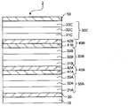
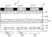
- FIG. 1 is a schematic cross-sectional view of one embodiment of the organic EL device of the present invention.
- the organic EL element 1 includes an anode 20, a first light emitting unit 30A, a charge generation layer 40, a second light emitting unit 30B, and a cathode 50 on a substrate 10 in this order.
- the first light emitting unit 30A and the second light emitting unit 30B emit light by recombination of electrons and holes.
- Each of the two light emitting units has a single layer or a stacked structure having at least light emitting layers 32A and 32B.
- the light emitting unit has a multilayer structure in which a hole transport layer 31, a light emitting layer 32, and an electron transport layer 33 are stacked from the anode side.
- the charge generation layer 40 generates holes and electrons when a voltage is applied, and injects holes into the light emitting unit disposed on the cathode 50 side of the charge generation layer 40, that is, the second light emitting unit 30B.
- This layer serves to inject electrons into the light emitting unit disposed on the anode 20 side of the charge generation layer 40, that is, the first light emitting unit 30A.
- the charge generation layer 40 has an N layer 41 formed on the anode side and a P layer 42 formed on the cathode side.
- the N layer 41 contains a compound represented by the following formula (I) or formula (II).
- R 1a to R 7a and R 1b to R 7b each independently represent a hydrogen atom, a substituted or unsubstituted aryl group having 6 to 60 ring carbon atoms, substituted or unsubstituted Substituted pyridyl group, substituted or unsubstituted quinolyl group, substituted or unsubstituted alkyl group having 1 to 50 carbon atoms, substituted or unsubstituted cycloalkyl group having 3 to 50 carbon atoms, substituted or unsubstituted ring-forming carbon 7 to 50 aralkyl groups, substituted or unsubstituted alkoxy groups having 1 to 50 carbon atoms, substituted or unsubstituted aryloxy groups having 6 to 50 ring carbon atoms, substituted or unsubstituted ring carbon atoms having 6 to 50 carbon atoms 50 arylthio groups, substituted or unsubsti
- L 1a and L 1b are each a single bond or a linking group.
- the linking group include a substituted or unsubstituted aromatic group having 6 to 20 ring carbon atoms, a substituted or unsubstituted alkylene chain having 1 to 8 carbon atoms, and a substituted or unsubstituted heterocyclic ring.
- a substituted or unsubstituted benzene ring, a substituted or unsubstituted naphthalene ring, a substituted or unsubstituted methylene chain, or a substituted or unsubstituted pyridine ring is preferable.
- Ar 1a and Ar 1b are each a substituted or unsubstituted aromatic group having 6 to 60 carbon atoms.
- n is 1 to 4, and when n is 2 or more, the groups having a phenanthroline skeleton in parentheses may be the same or different.
- R 1a to R 7a , R 1b to R 7b , L 1a and L 1b are each represented by the formula (I) And the same group as R 1a to R 7a , R 1b to R 7b , L 1a and L 1b in (II).
- R 11a to R 20a and R 11b to R 20b are each independently a hydrogen atom, a substituted or unsubstituted aryl group having 6 to 60 ring carbon atoms, a substituted or unsubstituted pyridyl group, a substituted or unsubstituted quinolyl.
- substituted or unsubstituted alkyl group having 1 to 50 carbon atoms substituted or unsubstituted cycloalkyl group having 3 to 50 carbon atoms, substituted or unsubstituted aralkyl group having 7 to 50 ring carbon atoms, substituted or unsubstituted Substituted alkoxy group having 1 to 50 carbon atoms, substituted or unsubstituted aryloxy group having 6 to 50 ring carbon atoms, substituted or unsubstituted arylthio group having 5 to 50 ring carbon atoms, substituted or unsubstituted carbon An alkoxycarbonyl group having 2 to 50 amino acids, an amino group substituted with a substituted or unsubstituted aryl group having 6 to 50 ring carbon atoms, a halogen atom, Anomoto, a nitro group, a hydroxyl group or a carboxyl group.
- R 11a to R 20a or R 11b to R 20b adjacent ones may be bonded to each other to form a ring.
- the ring include a benzene ring, a naphthalene ring, a pyrazine ring, a pyridine ring, and a furan ring.
- the aryl group includes a monocyclic aromatic hydrocarbon ring group and a condensed aromatic hydrocarbon ring group in which a plurality of hydrocarbon rings are condensed, and the heteroaryl group is a monocyclic heteroaromatic group.
- a hetero-fused aromatic ring group in which a plurality of heteroaromatic rings are condensed and a hetero-fused aromatic ring group in which an aromatic hydrocarbon ring and a heteroaromatic ring are condensed.
- Ring-forming carbon means a carbon atom constituting an aromatic ring
- ring-forming atom constitutes a heterocyclic ring (including a saturated ring, an unsaturated ring and an aromatic heterocyclic ring).
- the aryl group having 6 to 60 ring carbon atoms preferably has 6 to 30 carbon atoms, particularly preferably 6 to 20 carbon atoms.
- the aromatic group represented by Ar 1a and Ar 1b include the above-described aryl group and a bivalent or higher-valent group derived by removing a hydrogen atom from the aryl group.
- R 1a to R 7a and R 1b to R 7b in the formulas (I) and (II) are preferably hydrogen, phenyl, or naphthyl.
- alkyl group having 1 to 50 carbon atoms there is a linear or branched alkyl group.
- it has 1 to 20 carbon atoms, more preferably 1 to 12 carbon atoms, particularly preferably 1 to 8 carbon atoms, and examples thereof include methyl, ethyl, propyl, butyl, pentyl, hexyl and the like.
- Examples of the cycloalkyl group having 3 to 50 ring carbon atoms include cyclopentyl and cyclohexyl.
- the aralkyl group having 7 to 50 ring carbon atoms is represented by —Y—Z.
- Y include alkylene examples corresponding to the above alkyl groups, and examples of Z include the above aryl groups. Is mentioned.
- the aryl part of the aralkyl group preferably has 6 to 30 carbon atoms.
- the alkyl moiety preferably has 1 to 10 carbon atoms, particularly preferably 1 to 6 carbon atoms. For example, benzyl group, phenylethyl group, 2-phenylpropan-2-yl group.
- An alkoxy group having 1 to 50 carbon atoms is represented as —OY, and examples of Y include the above alkyl groups.
- the alkoxy group preferably has 1 to 20 carbon atoms, more preferably 1 to 12 carbon atoms, and particularly preferably 1 to 8 carbon atoms, and examples thereof include methoxy, ethoxy, propoxy, butoxy and the like.
- An aryloxy group having 6 to 50 ring carbon atoms is represented by —OY, and examples of Y include the above aryl groups.
- the number of carbon atoms is preferably 6 to 20, more preferably 6 to 16, and particularly preferably 6 to 12, and examples thereof include phenyloxy and 2-naphthyloxy.
- An arylthio group having 6 to 50 ring carbon atoms is represented by —SY, and examples of Y include the above aryl groups. Preferably it has 6 to 20 carbon atoms, more preferably 6 to 16 carbon atoms, particularly preferably 6 to 12 carbon atoms, and examples thereof include phenylthio.
- the alkoxycarbonyl group having 2 to 50 carbon atoms preferably has 2 to 20 carbon atoms, more preferably 2 to 16 carbon atoms, and particularly preferably 2 to 12 carbon atoms, and examples thereof include methoxycarbonyl and ethoxycarbonyl.
- Examples of the amino group substituted with a substituted or unsubstituted aryl group having 6 to 50 ring carbon atoms include diarylamino, alkylarylamino, and arylamino.
- Examples of the alkyl group and aryl group bonded to the nitrogen atom include the above-described aryl group and alkyl group. Preferably it has 6 to 20 carbon atoms, more preferably 6 to 12 carbon atoms, particularly preferably 6 carbon atoms, and examples thereof include diphenylamino and the like.
- halogen atom examples include a fluorine atom, a chlorine atom and a bromine atom, preferably a fluorine atom.
- Substituents for the above groups are each independently a linear or branched alkyl group having 1 to 20 carbon atoms, a linear or branched alkenyl group having 2 to 20 carbon atoms, or a ring-forming carbon number of 3
- aryl group examples include the aryl group, alkyl group, cycloalkyl group, heteroaryl group, alkoxy group, halogen atom, and cyano group. Furthermore, these groups may have a similar substituent.
- alkenyl group examples include a substituent having an unsaturated bond in the molecule of the alkyl group described above.
- silyl group having an aryl group examples include a triarylsilyl group, an alkylarylsilyl group, and a trialkylsilyl group.
- substituents include methyl, ethyl, propyl, isopropyl, butyl, sec-butyl, tert-butyl, cyclohexyl, phenyl, 1-naphthyl, 2-naphthyl, trimethylsilyl, triphenylsilyl.
- the N layer of the charge generation layer preferably contains at least one of an electron-donating metal, a metal compound, and a metal complex in addition to the compound of formula (I) or (II) described above.
- alkali metals, alkali metal compounds, organometallic complexes containing alkali metals, alkaline earth metals, alkaline earth metal compounds, organometallic complexes containing alkaline earth metals, rare earth metals, rare earth metal compounds, and rare earth metals It is preferable to contain at least one of organometallic complexes containing. Among these, it is preferable to contain at least one of an alkali metal, an alkaline earth metal, a rare earth metal, a rare earth metal compound, and a rare earth metal complex.
- alkali metal examples include lithium (Li), sodium (Na), potassium (K), rubidium (Rb), cesium (Cs) and the like, and those having a work function of 2.9 eV or less are particularly preferable. Of these, Li, K, Rb, and Cs are preferable, Li, Rb, and Cs are more preferable, and Li is most preferable.
- alkaline earth metal examples include calcium (Ca), magnesium (Mg), strontium (Sr), barium (Ba) and the like, and those having a work function of 2.9 eV or less are particularly preferable.
- rare earth metal examples include scandium (Sc), yttrium (Y), cerium (Ce), terbium (Tb), ytterbium (Yb) and the like, and those having a work function of 2.9 eV or less are particularly preferable.
- preferred metals are particularly high in reducing ability, and by adding a relatively small amount to the electron injection region, it is possible to improve the light emission luminance and extend the life of the organic EL element.
- alkali metal compound examples include lithium oxide (Li 2 O), cesium oxide (Cs 2 O), alkali oxides such as potassium oxide (K 2 O), lithium fluoride (LiF), sodium fluoride (NaF), fluorine.
- alkali halides such as cesium fluoride (CsF) and potassium fluoride (KF), and lithium fluoride (LiF), lithium oxide (Li 2 O), and sodium fluoride (NaF) are preferable.
- alkaline earth metal compound examples include barium oxide (BaO), strontium oxide (SrO), calcium oxide (CaO), and barium strontium oxide (Ba x Sr 1-x O) (0 ⁇ x ⁇ 1), Examples thereof include barium calcium oxide (Ba x Ca 1-x O) (0 ⁇ x ⁇ 1), and BaO, SrO, and CaO are preferable.
- the rare earth metal compound ytterbium fluoride (YbF 3), scandium fluoride (ScF 3), scandium oxide (ScO 3), yttrium oxide (Y 2 O 3), cerium oxide (Ce 2 O 3), gadolinium fluoride (GdF 3), include such terbium fluoride (TbF 3) is, YbF 3, ScF 3, TbF 3 are preferable.
- the organometallic complex is not particularly limited as long as it contains at least one of an alkali metal ion, an alkaline earth metal ion, and a rare earth metal ion as a metal ion as described above.
- the ligands include quinolinol, benzoquinolinol, acridinol, phenanthridinol, hydroxyphenyloxazole, hydroxyphenylthiazole, hydroxydiaryloxadiazole, hydroxydiarylthiadiazole, hydroxyphenylpyridine, hydroxyphenylbenzimidazole, hydroxybenzotriazole, Hydroxyfulborane, bipyridyl, phenanthroline, phthalocyanine, porphyrin, cyclopentadiene, ⁇ -diketones, azomethines, and derivatives thereof are preferred, but are not limited thereto.
- the addition form of the metal, compound and complex it is preferable to form a layer or island in the interface region.
- a forming method while vapor-depositing at least one of the above metal, compound and complex by resistance heating vapor deposition, an organic material which is a light emitting material or an electron injection material for forming an interface region is simultaneously deposited, and the above metal, A method of dispersing at least one of the compound and the complex is preferable.
- At least one of the metal, the compound and the complex in a layered form, after forming the light emitting material or the electron injecting material which is an organic layer at the interface in a layered form, at least one of the metal, the compound and the complex is singly used.
- Vapor deposition is performed by resistance heating vapor deposition, and the layer is preferably formed with a thickness of 0.1 nm to 15 nm.
- Vapor deposition is performed by a resistance heating vapor deposition method alone, and is preferably formed with an island thickness of 0.05 nm to 1 nm.
- the ratio is preferably 1: 1 to 1: 1, and more preferably 50: 1 to 4: 1.
- the organic EL device of the present invention only needs to use the compound represented by the above formula (I) or (II) for the N layer of the charge generation layer, and other components such as an anode, a light emitting unit, a cathode, etc. Any known member in this technical field can be used as appropriate. Hereinafter, each member which comprises the organic EL element of this invention is demonstrated.
- the organic EL device of the present invention is produced on a substrate.
- the substrate supports the organic EL element.
- the substrate needs to be translucent.
- the light transmittance in the visible region of 400 to 700 nm is preferably 50% or more.
- a glass plate, a polymer plate, etc. are mentioned.
- the glass plate include soda lime glass, barium / strontium-containing glass, lead glass, aluminosilicate glass, borosilicate glass, barium borosilicate glass, and quartz.
- the polymer plate include polycarbonate, acrylic, polyethylene terephthalate, polyether sulfide, and polysulfone.
- translucency is unnecessary when a support substrate is located on the opposite side to the light extraction direction.
- the anode of the organic EL element plays a role of injecting holes into the hole transport layer or the light emitting layer.
- ITO indium tin oxide alloy
- NESA tin oxide
- IZO indium zinc oxide alloy
- gold silver, platinum, copper, or the like
- metals such as silver, aluminum, molybdenum, chromium, nickel, and alloys with other metals can be used. .
- the anode can be produced by forming a thin film from these electrode materials by a method such as vapor deposition or sputtering.
- the transmittance of the anode for light emission is preferably greater than 10%.
- the sheet resistance of the anode is preferably several hundred ⁇ / ⁇ or less.
- the film thickness of the anode depends on the material, it is usually selected in the range of 10 nm to 1 ⁇ m, preferably 10 to 200 nm.
- the light emitting unit has a single layer or a stacked structure including at least a light emitting layer.
- the light emitting unit preferably has a multilayer film structure composed of a first organic layer, a light emitting layer, and a second organic layer from the anode side.
- a multilayer composed of a hole transport zone / a light emitting layer / an electron transport zone. Examples include a membrane structure.
- the hole transport zone is configured by laminating a single layer or a plurality of hole injection layers and hole transport layers.
- the electron transport zone is configured by laminating a single layer or a plurality of electron injection layers and electron transport layers.
- each light emitting unit may be made of the same material, or may be made of different materials. Further, the layer configuration of each light emitting unit may be the same or different. For example, in the organic EL element shown in FIG. 1, the electron transport layer of the first light emitting unit 30A may be omitted, and a two-layer structure including a hole transport layer 31A and a light emitting layer 32A may be used. Furthermore, the emission color of each light emitting unit may be the same or different. For example, in the element 1 shown in FIG. 1, the emission color of the first light emitting unit 30A may be yellow, and the emission color of the second light emitting unit 30B may be blue. In this case, an organic EL element that emits white light by mixing two lights is obtained.
- the light emitting layer, the hole transport zone, and the electron transport zone constituting the light emitting unit will be described.
- the layer comprised from host material and dopant material is preferable.
- the host material of the organic EL element rubrene, anthracene, tetracene, pyrene, perylene and the like can be used.
- it is an anthracene derivative, More preferably, the anthracene derivative represented by following formula (1) is included.
- Ar 11 and Ar 12 are each a substituted or unsubstituted aryl group having 6 to 30 ring carbon atoms or a substituted or unsubstituted heterocyclic group having 5 to 30 ring atoms.
- R 101 to R 108 are each a hydrogen atom, a fluorine atom, a substituted or unsubstituted alkyl group having 1 to 10 carbon atoms, a substituted or unsubstituted cycloalkyl group having 3 to 10 carbon atoms, or a substituted or unsubstituted carbon number.
- Examples of the luminescent dopant include a fluorescent dopant and a phosphorescent dopant.
- a fluorescent dopant is a compound that can emit light from singlet excitons. Fluorescent dopants are required from amine compounds, aromatic compounds, chelate complexes such as tris (8-quinolinolato) aluminum complex, coumarin derivatives, tetraphenylbutadiene derivatives, bisstyrylarylene derivatives, oxadiazole derivatives, etc.
- a compound selected according to the emission color is preferable, a styrylamine compound, a styryldiamine compound, an arylamine compound, an aryldiamine compound, and an aromatic compound are more preferable, and a condensed polycyclic amine derivative and an aromatic compound are further preferable.
- These fluorescent dopants may be used alone or in combination.
- Y represents a substituted or unsubstituted condensed aryl group having 10 to 50 ring carbon atoms.
- Ar 21 and Ar 22 each represent a substituted or unsubstituted aryl group having 6 to 50 ring carbon atoms or a substituted or unsubstituted heterocyclic group having 5 to 50 ring atoms.
- the condensed aryl group is a group in which two or more ring structures are condensed in the aryl group.
- the condensed aryl group is a condensed aryl group having 10 to 50 ring carbon atoms (preferably 10 to 30 ring carbon atoms, more preferably 10 to 20 ring carbon atoms).
- Preferred examples include naphthyl group, anthryl group, pyrenyl group, chrysenyl group, phenanthryl group, fluorenyl group, fluoranthenyl group, acenaphthofluoranthenyl group, naphthacenyl group and the like.
- Y include the above-mentioned fused aryl groups, preferably a substituted or unsubstituted anthryl group, a substituted or unsubstituted pyrenyl group, a substituted or unsubstituted chrysenyl group, or an acenaphthofluoranthenyl group.
- Ar 21 and Ar 22 include a substituted or unsubstituted phenyl group and a substituted or unsubstituted dibenzofuranyl group.
- Preferred examples of the substituent for Ar 21 and Ar 22 include an alkyl group, a cyano group, and a substituted or unsubstituted silyl group.
- n is an integer of 1 to 4.
- n is preferably an integer of 1 to 2.
- a fluoranthene compound represented by the following formula (3) is preferable.
- X 101 to X 106 and X 108 to X 111 each independently represents a hydrogen atom, a substituted or unsubstituted aryl group having 6 to 30 ring carbon atoms, a substituted or unsubstituted ring atom number of 5;
- X 107 and X 112 are each independently a substituted or unsubstituted aryl group having 6 to 30 ring carbon atoms, a substituted or unsubstituted heterocyclic group having 5 to 30 ring atoms, a substituted or unsubstituted carbon atom, It is selected from alkyl groups having 1 to 20 and substituted or unsubstituted cycloalkyl groups having 3 to 8 ring carbon atoms.
- X103 and X104 are mutually different substituents.
- adjacent substituents may be bonded to each other to form a saturated or unsaturated cyclic structure, and these cyclic structures may be substituted.
- X 103 or X 104 in formula (3) is preferably a substituted or unsubstituted aryl group having 6 to 30 ring carbon atoms. Further, a preferred substituent of “substituted or unsubstituted” in formula (3) is a cyano group or a halogen atom.
- aryl group, heterocyclic group, alkyl group, cycloalkyl group, alkoxy group, aralkyl group, aryloxy group, arylthio group, alkoxycarbonyl group and halogen atom is done.
- a host suitable for phosphorescence emission is a compound having a function of causing the phosphorescence emission compound to emit light as a result of energy transfer from the excited state to the phosphorescence emission compound.
- the host compound is not particularly limited as long as it has a large triplet energy gap and can transfer exciton energy to the phosphorescent compound, and can be appropriately selected according to the purpose.
- host compounds include condensed ring compounds composed of combinations of benzene rings, naphthalene rings, and heterocyclic rings, carbazole derivatives, triazole derivatives, oxazole derivatives, oxadiazole derivatives, imidazole derivatives, polyarylalkane derivatives.
- a phosphorescent dopant is a compound that can emit light from triplet excitons. Although it is not particularly limited as long as it emits light from a triplet exciton, it is preferably a metal complex containing at least one metal selected from the group consisting of Ir, Ru, Pd, Pt, Os and Re, and a porphyrin metal complex or ortho Metalated metal complexes are preferred.
- the porphyrin metal complex is preferably a porphyrin platinum complex.
- the phosphorescent compounds may be used alone or in combination of two or more.
- ligands for forming orthometalated metal complexes include 2-phenylpyridine derivatives, 7,8-benzoquinoline derivatives, and 2- (2-thienyl) pyridine derivatives. 2- (1-naphthyl) pyridine derivatives, 2-phenylquinoline derivatives, and the like. These derivatives may have a substituent if necessary.
- a fluorinated compound or a compound having a trifluoromethyl group introduced is preferable as a blue dopant.
- the content of the phosphorescent dopant in the light emitting layer is not particularly limited and may be appropriately selected depending on the intended purpose. For example, it is 0.1 to 70% by mass, and 1 to 30% by mass. preferable. When the content of the phosphorescent compound is 0.1% by mass or more, it is possible to prevent the emission of light from being weakened and to sufficiently exhibit the content effect. By setting the content to 70% by mass or less, a phenomenon called concentration quenching can be suppressed and deterioration of device performance can be prevented.
- the light emitting layer may contain a hole transport material, an electron transport material, and a polymer binder as necessary.
- the thickness of the light emitting layer is preferably 5 to 50 nm, more preferably 7 to 50 nm, and most preferably 10 to 50 nm. When the thickness is 5 nm or more, the light emitting layer can be easily formed and the chromaticity can be easily adjusted. By setting the thickness to 50 nm or less, it is possible to prevent the drive voltage from increasing.
- Hole transport zone Layers in the hole transport zone include a hole transport layer and a hole injection layer.
- the hole transport layer is a layer that assists hole injection into the light emitting layer and transports it to the light emitting region, and has a high hole mobility and a small ionization energy of usually 5.5 eV or less.
- Such a hole transport layer is preferably a material that transports holes to the light-emitting layer with a lower electric field strength, and further has a hole mobility of at least 10 when an electric field of 10 4 to 10 6 V / cm is applied. -4 cm 2 / V ⁇ sec is preferred.
- the material for the hole transport layer include, for example, triazole derivatives, oxadiazole derivatives, imidazole derivatives, polyarylalkane derivatives, pyrazoline derivatives and pyrazolone derivatives, phenylenediamine derivatives, arylamine derivatives, amino-substituted chalcone derivatives, oxazole derivatives. , Styrylanthracene derivatives, fluorenone derivatives, hydrazone derivatives, stilbene derivatives, silazane derivatives, polysilanes, aniline copolymers, conductive polymer oligomers (particularly thiophene oligomers), and the like.
- an aromatic amine compound for example, an aromatic amine derivative represented by the following formula (4) is preferably used.
- Ar 31 to Ar 34 each represent an aromatic hydrocarbon group having 6 to 50 ring carbon atoms (which may have a substituent), a condensed aromatic group having 6 to 50 ring carbon atoms.
- L represents a single bond or a group similar to Ar 31 to Ar 34 .
- aromatic amine of following formula (5) is also used suitably for formation of a positive hole injection layer or a positive hole transport layer.
- the hole injection layer is a layer provided to further assist hole injection.
- the material for the hole injection layer may be the organic EL material of the present invention alone, or may be used in combination with other materials. As other materials, the same materials as the hole transport layer can be used.
- a porphyrin compound, an aromatic tertiary amine compound, and a styrylamine compound can also be used.
- HAT or F4TCNQ used in the P layer of the charge generation layer, or a compound represented by the formula (4) can also be used.
- conductive oligomers such as thiophene-containing oligomers, arylamine oligomers disclosed in JP-A-8-193191, conductive dendrimers such as arylamine dendrimers, and the like can also be used.
- inorganic compounds such as p-type Si and p-type SiC can also be used as the material for the hole injection layer.
- the hole injection layer or the hole transport layer can be formed, for example, by thinning the above-described compound by a known method such as a vacuum deposition method, a spin coating method, a casting method, or an LB method.
- the thickness of the hole injection layer or hole transport layer is not particularly limited, but is usually 1 nm to 5 ⁇ m.
- Electron transport zone Layers of the electron transport zone include an electron injection layer and an electron transport layer (hereinafter referred to as an electron injection layer / transport layer).
- the electron injection layer / transport layer assists the injection of electrons into the light emitting layer and transports it to the light emitting region, and has a high electron mobility.
- the electron injecting layer / transporting layer is appropriately selected with a film thickness of several nm to several ⁇ m. In particular, when the film thickness is large, in order to avoid an increase in voltage, the electron mobility is applied when an electric field of 10 4 to 10 6 V / cm is applied. Is preferably at least 10 ⁇ 5 cm 2 / Vs or more.
- 8-hydroxyquinoline or a metal complex of its derivative or a nitrogen-containing heterocyclic derivative is preferable.
- a metal chelate oxinoid compound containing a chelate of oxine (generally 8-quinolinol or 8-hydroxyquinoline), for example, tris (8-quinolinol) aluminum is injected. It can be used as a material.
- nitrogen-containing heterocyclic derivative for example, oxazole, thiazole, oxadiazole, thiadiazole, triazole, pyridine, pyrimidine, triazine, phenanthroline, benzimidazole, imidazopyridine and the like are preferable, and among them, benzimidazole derivative, phenanthroline derivative, imidazopyridine derivative Is preferred.
- the charge generation layer injects holes into the light emitting unit disposed on the cathode side of the charge generation layer, while injecting electrons into the light emission unit disposed on the anode side of the charge generation layer. It is a layer that plays a role.
- the charge generation layer has an N layer formed on the anode side and a P layer formed on the cathode layer side.
- the N layer is as described above.
- the thickness of the N layer is preferably 0.1 nm to 100 nm, and particularly preferably 1 nm to 50 nm.
- Examples of the P layer include a layer containing a compound represented by the following formula (III).
- the compound represented by the formula (III) is used in the charge generation layer because it improves the characteristics of the device, such as efficiency, voltage, and lifetime. However, since the compound of formula (III) itself has high conductivity, current leakage between pixels through the charge generation layer may occur. By combining the N layer of the present invention and the layer containing the compound represented by formula (III), current leakage between adjacent pixels can be suppressed.
- R 1c to R 6c in the formula are each independently a hydrogen atom, a substituted or unsubstituted aryl group having 6 to 60 ring carbon atoms, a substituted or unsubstituted pyridyl group, a substituted or unsubstituted quinolyl group, a substituted Or an unsubstituted alkyl group having 1 to 50 carbon atoms, a substituted or unsubstituted cycloalkyl group having 3 to 50 carbon atoms, a substituted or unsubstituted aralkyl group having 7 to 50 ring carbon atoms, and a substituted or unsubstituted carbon.
- the layer containing the compound represented by following formula (IV) is mentioned.
- Ar 1 is an aromatic ring having 6 to 24 ring carbon atoms or a heterocyclic ring having 5 to 24 ring atoms, preferably an aromatic ring having 6 to 14 ring carbon atoms or the number of ring forming atoms. 5-14 heterocycles.
- the aromatic ring include a benzene ring, a naphthalene ring, a fluorene ring, a 9,9-dimethylfluorene ring, and a 9,9-dioctylfluorene ring.
- heterocyclic ring examples include a pyrazine ring, a pyridine ring, a quinoxaline ring, a thiophene ring, a benzothiophene ring, a dibenzothiophene ring, a furan ring, a benzofuran ring, a dibenzofuran ring, a phenanthroline ring, a naphthyridine ring, and a tetraazaanthracene ring.
- the aromatic ring and heterocyclic ring are substituted or unsubstituted alkyl groups, substituted or unsubstituted cycloalkyl groups, substituted or unsubstituted alkenyl groups, substituted or unsubstituted aryl represented by R 1 to R 4 described below.
- R 1 to R 4 may be the same as or different from each other, and are a hydrogen atom, a substituted or unsubstituted alkyl group, a substituted or unsubstituted cycloalkyl group, a substituted or unsubstituted alkenyl group.
- R 1 and R 2 and R 3 and R 4 may be bonded to each other to form a ring.
- alkyl group examples include methyl group, ethyl group, n-propyl group, isopropyl group, n-butyl group, isobutyl group, tert-butyl group, octyl group and the like.
- cycloalkyl group examples include a cyclopentyl group and a cyclohexyl group.
- Alkenyl groups include vinyl groups, propenyl groups (including double bond positional isomers), butenyl groups (including double bond positional isomers), pentenyl groups (including double bond positional isomers), etc. Can be mentioned.
- aryl group phenyl group, biphenyl group, naphthyl group, fluorophenyl group, trifluoromethylphenyl group, (trifluoromethyl) fluorophenyl group, trifluorophenyl group, bis (trifluoromethyl) phenyl group, (Trifluoromethyl) difluorophenyl group, trifluoromethoxyphenyl group, trifluoromethoxyfluorophenyl group and the like can be mentioned.
- heterocyclic group include residues such as pyridine, pyrazine, furan, imidazole, benzimidazole, and thiophene.
- halogen atom examples include a fluorine atom, a chlorine atom, a bromine atom, and an iodine atom.
- fluoroalkyl group examples include a trifluoromethyl group, a pentafluoroethyl group, a perfluorocyclohexyl group, and a perfluoroadamantyl group.
- alkoxy group examples include a methoxy group and an ethoxy group.
- fluoroalkoxy group examples include trifluoromethoxy group, pentafluoroethoxy group, 2,2,2-trifluoroethoxy group, 2,2,3,3,3-pentafluoropropoxy group, 2,2,3,3- Examples thereof include a tetrafluoropropoxy group and a 1,1,1,3,3,3-hexafluoropropan-2-yloxy group.
- (substituted) aryloxy groups include phenyloxy group, pentafluorophenyloxy group, 4-trifluorophenyloxy group and the like.
- Examples of (substituted) aralkyloxy groups include benzyloxy group, pentafluorobenzyloxy group, 4-trifluoromethylbenzyloxy group and the like.
- Examples of (substituted) amino groups include amino groups, mono- or dimethylamino groups, mono- or diethylamino groups, mono- or diphenylamino groups, and the like.
- Examples of (substituted) silyl groups include silyl groups, mono-, di- or trimethylsilyl groups, mono-, di- or triethylsilyl groups, mono-, di- or triphenylsilyl groups.
- Examples of the optional substituent for R 1 to R 4 include the halogen atom, cyano group, alkyl group, aryl group, fluoroalkyl group, fluoroalkoxy group and heterocyclic group mentioned above.
- examples of the optional substituents referred to as “substituted or unsubstituted” include the halogen atoms, cyano groups, alkyl groups, aryl groups, fluoroalkyl groups, fluoroalkoxy groups, and heterocycles mentioned above.
- a cyclic group is mentioned.
- R 1 and R 2 and R 3 and R 4 may be bonded to each other to form a ring.
- the ring include a benzene ring, a naphthalene ring, a pyrazine ring, a pyridine ring, and a furan ring.
- at least one of R 1 to R 4 is a fluorine atom, a fluoroalkyl group, a fluoroalkoxy group, a cyano group, or at least one group selected from fluorine, a fluoroalkyl group, a fluoroalkoxy group, and a cyano group.
- An aryl group or a heterocyclic group is preferable. By using these as substituents, electron acceptability can be increased, an appropriate sublimation temperature can be obtained, or crystallization can be suppressed.
- Rg 1 and Rg 2 in the formula (IV) may be the same or different from each other, and are represented by the following formula (i) or (ii).
- X 1 and X 2 may be the same or different from each other, and are any of the divalent groups shown in the following (a) to (g). In particular, (a) to (c) are preferable from the viewpoints of excellent heat resistance or ease of synthesis.
- R 21 to R 24 may be the same or different from each other, and are a hydrogen atom, a substituted or unsubstituted fluoroalkyl group, a substituted or unsubstituted alkyl group, a substituted or unsubstituted cycloalkyl group, A substituted or unsubstituted aryl group or a substituted or unsubstituted heterocyclic group, R 22 and R 23 may be bonded to each other to form a ring.
- Specific examples of the fluoroalkyl group, the alkyl group, the cycloalkyl group, the aryl group, and the heterocyclic group include the groups exemplified for R 1 to R 4 .
- Y 1 to Y 4 may be the same as or different from each other, and each represents N, CH, or C (R 5 ), and R 5 represents the same group as R 1 to R 4 . Further, it is preferable that at least one of Y 1 to Y 4 is a nitrogen atom (the same applies to Y 21 to Y 26 and Y 31 to Y 38 described later). Since at least one is a nitrogen atom, electron acceptability can be increased, heat resistance can be increased, or crystallization can be suppressed.
- the indenofluorangeone derivative of formula (IV) is preferably represented by the following formula (IV-A) or (IB).
- Each symbol such as Ar 1 in the following formula (IV-A) has the same meaning as in formula (IV).
- Ar 2 in the following formula (IV-B) is synonymous with Ar 1 in the formula (IV)
- X 3 and X 4 are synonymous with X 1 and X 2 in the formula (IV)
- Y 5 to Y 8 has the same meaning as Y 1 ⁇ Y 4 in formula (IV)
- R 1 ⁇ R 4 have the same meanings as R 1 ⁇ R 4 in formula (IV).
- the indenofluorangeone derivative of the formula (IV) is represented by the following formulas (IVa) to (IVi).
- R 1 ⁇ R 4 have the same meanings as X 1 and X 2, R 1 ⁇ R 4 in formula (IV), Y 21 ⁇ Y 26, Y 31 ⁇ Y 38 and, Y 41 to Y 50 have the same meanings as Y 1 to Y 4 in formula (IV).
- Particularly preferred indenofluorangeone derivatives of the formula (IV) are represented by the following formulas (IV-a) to (IV-n).
- the following formulas (IV-b), (IV-d), (IV-f), (IV-h), (IV-j), (IV-l), (IV-n), (IV-p) ) And (IV-r) have a plurality of isomers depending on the configuration of the cyano groups of the two cyanoimino groups.
- the present invention is not limited to a specific isomer.
- the invention may be a specific isomer alone or a mixture of two or more than two isomers.
- R 31 to R 52 have the same meanings as R 1 to R 4 in formula (IV).
- R 31 to R 52 adjacent to each other may be bonded to each other to form a ring.
- at least one of R 31 to R 52 is a fluorine atom, a fluoroalkyl group, a fluoroalkoxy group, a cyano group, or an aryl having at least one group selected from fluorine, a fluoroalkyl group, a fluoroalkoxy group, and a cyano group It is preferably a group or a heterocyclic group.
- the indenofluorangeone derivative has the structure of each of the above formulas, it has electron acceptability, is excellent in heat resistance, has a sublimation temperature of about 200 ° C. or higher, and can be purified by sublimation. High purity can be achieved. Moreover, the drive voltage of an element can be reduced by using it for an organic EL element, and lifetime can be improved. Furthermore, since the sublimation temperature is about 200 ° C. or higher during the manufacture of the element, it does not scatter inside the deposition film forming apparatus, so that the film forming apparatus or the organic EL element is not contaminated.
- indenofluorangeone derivative of the formula (IV) are shown below, but are not limited thereto.
- the P layer may be a layer made of only the compound represented by the formula (IV) or a layer made of a mixture with other materials.
- the P layer is preferably a layer containing a compound represented by the formula (IV) and at least one hole transport material.
- the hole transport material materials used in the above-described hole transport zone can be used. Of these, aromatic tertiary amine compounds are preferred.
- the content of the compound represented by the formula (IV) in the P layer is preferably 0.1% by weight to 100% by weight, and particularly preferably 10% by weight to 70% by weight.
- the thickness of the P layer is preferably 1 nm to 50 nm, and particularly preferably 5 nm to 20 nm.
- At least one of the light emitting units has a hole transport layer, and the P layer of the charge generation layer is in contact with the hole transport layer.
- the hole transport layer 31B of the second light emitting unit 30B and the P layer 42 of the charge generation layer are preferably in contact with each other. This efficiently injects holes from the charge generation layer into the hole transport layer 31B of the second light emitting unit 30B, thereby lowering the voltage of the device.
- the charge generation layer may consist of only two layers, an N layer and a P layer, or may have an intervening layer between the N layer and the P layer.
- cathode As the cathode, a metal, an alloy, an electrically conductive compound having a low work function (4 eV or less), and a mixture thereof and an electrode material thereof are used. Specific examples of such electrode materials include sodium, sodium-potassium alloy, magnesium, lithium, magnesium / silver alloy, aluminum, aluminum / aluminum oxide, aluminum / lithium alloy, indium, and rare earth metals.
- the cathode can be produced by forming a thin film of these electrode materials by a method such as vapor deposition or sputtering.
- the transmittance with respect to the light emitted from the cathode is larger than 10%.
- the sheet resistance as the cathode is preferably several hundred ⁇ / ⁇ or less, and the film thickness is usually 10 nm to 1 ⁇ m, preferably 50 to 200 nm.
- an electron injection layer made of an insulator or a semiconductor may be provided between the cathode and the organic layer.
- an insulator it is preferable to use at least one metal compound selected from the group consisting of alkali metal chalcogenides, alkaline earth metal chalcogenides, alkali metal halides and alkaline earth metal halides. If the electron injection layer is composed of these alkali metal chalcogenides or the like, it is preferable in that the electron injection property can be further improved.
- preferable alkali metal chalcogenides include, for example, Li 2 O, LiO, Na 2 S, Na 2 Se, and NaO
- preferable alkaline earth metal chalcogenides include, for example, CaO, BaO, SrO, and BeO. , BaS, and CaSe
- preferable alkali metal halides include, for example, LiF, NaF, KF, CsF, LiCl, KCl, and NaCl.
- preferable alkaline earth metal halides include fluorides such as CaF 2 , BaF 2 , SrF 2 , MgF 2 and BeF 2 , and halides other than fluorides.
- the semiconductor constituting the electron injection layer includes Ba, Ca, Sr, Yb, Al, Ga, In, Li, Na, Cd, Mg, Si, Ta, Sb, and an oxide or nitride containing at least one element of Zn.
- the inorganic compound constituting the electron injection layer is preferably a microcrystalline or amorphous insulating thin film. Examples of such inorganic compounds include the alkali metal chalcogenides, alkaline earth metal chalcogenides, alkali metal halides, and alkaline earth metal halides described above.
- the form of the organic EL element of the present invention has been described by exemplifying the organic EL element 1 of FIG. 1, but the present invention is not limited to the form of the organic EL element 1.
- the organic EL element 1 two light emitting units are formed, but three or more light emitting units may be formed.
- FIG. 2 is a schematic cross-sectional view of an organic EL device according to the second embodiment of the present invention.
- the organic EL element 2 includes the anode 20, the first light emitting unit 30A, the first charge generating layer 40A, the second light emitting unit 30B, the second charge generating layer 40B, and the third light emitting unit 30C on the substrate 10. And the cathode 50 are provided in this order.
- the organic EL element 2 has the same configuration as the organic EL element 1 shown in FIG. 1 except that three light emitting units are formed and two charge generation layers are formed.
- the first charge generation layer 40A (N layer 41A, P layer 42A) corresponds to the charge generation layer 40
- the second charge generation layer 40B N layer 41B, P layer 42B
- the units 30C (the hole transport layer 31C, the light emitting layer 32C, and the electron transport layer 33C) are the same as those described above.
- the emission color of each light emitting unit for example, by changing the emission color of each light emitting unit to red, green, and blue, it is possible to obtain a white light emitting EL element with high color rendering properties that harmoniously includes light in three wavelength regions.
- FIG. 3 is a schematic view showing an example in which three organic EL elements are formed on a substrate.
- the first light emitting unit 30A, the charge generation layer 40, and the second light emitting unit 30B are formed in this order in common on the substrate 10 and each anode.
- On the second light emitting unit 30 ⁇ / b> B, the cathode 50 is formed in a stripe shape so as to be orthogonal to the anode 20.
- the organic EL elements A to C emit light when a voltage is applied between the anodes 20A to 20C and the cathode 50 facing each other. For example, when a voltage is applied between the anode 20B and the cathode 50, the element B emits light.
- the charge flows to the adjacent element through the charge generation layer formed in common between the elements, and as a result, originally emits light. There was a problem that neighboring elements that should not emit light. As a result, the light emission efficiency and the color purity of the display device are reduced.
- the organic EL device of the present invention by using the compound of formula (I) or (II) described above for the N layer of the charge generation layer, leakage of charges to adjacent devices can be suppressed.
- the organic EL element of the present invention is particularly suitable as a light emitting element of a color display device using a color filter.
- FIG. 4 is a schematic sectional view of a color display device using the organic EL element of the present invention.
- a color filter 60 having a red color filter (RCF) 61, a green color filter (GCF) 62, and a blue color filter (BCF) 63 is formed on the light extraction side of the organic EL element shown in FIG. It is.
- the light emitting color of the first light emitting unit 30A is yellow
- the light emitting color of the second light emitting unit 30B is blue, whereby an organic EL element that emits white light is obtained. Only a desired color is extracted from the white light to the outside of the display device by the color filter.
- the organic EL device of the present invention can suppress charge leakage to adjacent devices. That is, unnecessary light emission of adjacent elements can be reduced and only desired elements (pixels) can emit light, so that the color reproducibility of the display device can be improved.
- the organic EL device of the present invention can be produced by a known method.
- the anode and the cathode can be formed by a method such as vapor deposition or sputtering.
- Each organic layer such as a light emitting unit can be formed by a method such as vacuum deposition, spin coating, casting, or LB.
- ITO was formed to a thickness of 240 nm as an anode on a substrate made of a 30 mm ⁇ 30 mm glass plate.
- a cell for an organic EL element in which a region other than the light emitting region of 2 mm ⁇ 2 mm was masked with an insulating film (not shown) by SiO 2 vapor deposition was produced.
- hexanitrile azatriphenylene (HAT) having the above structure was formed as a hole injection layer with a thickness of 10 nm.
- a blue light-emitting unit (first light-emitting unit) composed of a hole transport layer, a blue light-emitting layer, and an electron transport layer was formed on the hole injection layer.
- the ⁇ -NPD was formed as a hole transport layer with a film thickness of 90 nm (deposition rate: 0.2 to 0.4 nm / sec) by vacuum evaporation. Subsequently, a blue light emitting layer was formed on the hole transport layer.
- the compound of the above formula (1) was used as the host of the light emitting layer, and the compound of the formula (2) was used as the dopant. Vacuum deposition was performed so that the added amount of the dopant was 5% in terms of the film thickness ratio to obtain a light emitting layer having a film thickness of 30 nm.
- the Alq3 was formed to a thickness of 30 nm as an electron transport layer on the blue light emitting layer.
- a charge generation layer was formed following the blue light emitting unit.
- an N layer and a P layer were formed in this order using the compounds shown in Table 1.
- the N layer and the P layer were not formed. In either case, the thickness was 10 nm.
- the N layer is a mixed layer of the compounds in Table 1 and Li.
- a second blue light emitting unit was formed. The formation method was the same as that of the first blue light emitting unit described above.
- LiF is formed with a film thickness of about 0.3 nm (deposition rate ⁇ 0.01 nm / sec) by a vacuum evaporation method, and then Al is formed with a film thickness of 200 nm by a vacuum evaporation method.
- LiF is formed with a film thickness of about 0.3 nm (deposition rate ⁇ 0.01 nm / sec) by a vacuum evaporation method
- Al is formed with a film thickness of 200 nm by a vacuum evaporation method.
- planarization insulating film was formed on a glass substrate.
- the planarization insulating film material is not particularly limited as long as it is a positive photosensitive insulating material, but here, polyimide is formed to a thickness of 2.0 ⁇ m.
- Polyimide was applied onto the substrate by spin coating, exposed with an exposure device, developed with a paddle type developing device, and patterned into a predetermined shape. In order to cure the polyimide, main baking was performed in a clean baking furnace to form a planarization insulating film having a thickness of 2.0 ⁇ m. Next, a lower electrode was formed on the planarization insulating film.
- An ITO film having a thickness of 240 nm was formed on the planarization insulating film, and patterned and etched into a predetermined shape using a normal lithography technique to form a lower electrode. Between the patterned lower electrodes (ITO), polyimide was formed to a thickness of 2.0 ⁇ m to form an interelectrode insulating layer.
- the interelectrode insulating layer was formed by applying polyimide on a substrate by spin coating, exposing with an exposure device, and developing with a paddle type developing device. Thus, polyimide, which is a photosensitive insulating material, is patterned into a predetermined shape. Next, in order to cure the polyimide, a main baking was performed in a clean baking furnace to form an interelectrode insulating layer.
- a yellow light-emitting unit (first light-emitting unit) composed of a hole transport layer, a yellow light-emitting layer and an electron transport layer was formed on the hole injection layer composed of hexanitrile azatriphenylene (HAT).
- HAT hexanitrile azatriphenylene
- the ⁇ -NPD was formed with a film thickness of 30 nm (deposition rate: 0.2 to 0.4 nm / sec) by vacuum evaporation.
- a yellow light emitting layer was formed on the hole transport layer.
- a compound represented by the following formula (3) was used as the host of the light emitting layer, and a compound represented by the formula (4) was used as the dopant.
- Vacuum deposition was performed so that the added amount of the dopant was 5% in terms of the film thickness ratio to obtain a light emitting layer having a film thickness of 30 nm.
- the Alq3 was formed to a thickness of 20 nm as an electron transport layer on the yellow light-emitting layer.
- the voltage (V) and luminance (cd / m 2 ) at a current density of 10 mAcm ⁇ 2 , and the relative luminance value after 300 hours at 50 mA / cm 2 drive were measured for the produced organic EL device. did. Further, the CIE chromaticity of light emission was obtained by a spectral radiance meter. The results are shown in Table 2.
- red, green, and blue color filters were formed on each pixel of the organic EL elements produced in Examples 16 and 17 and Comparative Examples 5 and 6, and the color reproducibility included in each RGB color was evaluated by NTSC ratio. .
- the organic EL device was manufactured as follows.
- the RGB color filters were formed in order on the glass substrate at the openings, and a planarization insulating film was formed thereon to planarize the unevenness of the color filters. This obtained the glass substrate which has a color filter. Thereafter, a patterned electrode substrate was produced in the same manner as in Example 5, and a light emitting unit was further formed. In the fabricated device, an upper electrode and a lower electrode are wired so that passive driving is possible so that each pixel of RGB can emit light individually. As a result, it is possible to emit light in each of the RGB colors.
- the NTSC ratio is the standard three primary colors defined by the US National Television System Committee (NTSC), red (0.670, 0.330), and green (0.210, 0.710).
- FIG. 5 shows regions obtained by connecting the chromaticity coordinates of red, green, and blue determined by NTSC in the XYZ color system chromaticity diagram. This area is 100%. The results are shown in Table 2.
- the organic EL device of the present invention can be used for a flat light emitter such as a flat panel display of a wall-mounted television, a copying machine, a printer, a light source such as a backlight of a liquid crystal display or instruments, a display board, a marker lamp, and the like.
- a flat light emitter such as a flat panel display of a wall-mounted television, a copying machine, a printer, a light source such as a backlight of a liquid crystal display or instruments, a display board, a marker lamp, and the like.
Landscapes
- Chemical & Material Sciences (AREA)
- Organic Chemistry (AREA)
- Physics & Mathematics (AREA)
- Spectroscopy & Molecular Physics (AREA)
- Engineering & Computer Science (AREA)
- Materials Engineering (AREA)
- Optics & Photonics (AREA)
- Electroluminescent Light Sources (AREA)
- Nitrogen Condensed Heterocyclic Rings (AREA)
- Organic Low-Molecular-Weight Compounds And Preparation Thereof (AREA)
Abstract
Description
この問題を解決するためには、駆動電流を変えずに輝度を上げる、即ち効率を改善するか、或いは駆動電流を下げても同様の輝度を得ることができる素子構成を実現する必要がある。 The lifetime of the organic EL element is generally determined by the amount of injected charge. For this reason, when the drive current is increased to increase the initial luminance, there is a problem that the lifetime is shortened accordingly.
In order to solve this problem, it is necessary to increase the luminance without changing the driving current, that is, to improve the efficiency, or to realize an element configuration that can obtain the same luminance even if the driving current is decreased.
電荷発生層を介して発光ユニットを積層させたスタック型の有機EL素子では、2つの発光ユニットを積層した場合には、理想的には発光効率[lm/W]は変ること無しに輝度[cd/A]を2倍に、3つの発光ユニットを積層した場合には、理想的には発光効率は変ること無しに輝度を3倍にすることが可能であるとされている。 As the above-described element configuration, a structure (MPE element) is proposed in which a plurality of light-emitting units composed of an organic layer having at least a light-emitting layer are disposed between an anode and a cathode via an insulating charge generation layer. ing. Here, the charge generation layer injects holes into the light emitting unit arranged on the cathode side of the charge generation layer and applies the voltage to the light emitting unit arranged on the anode side of the charge generation layer. This layer serves to inject electrons.
In a stack type organic EL element in which light emitting units are stacked via a charge generation layer, when two light emitting units are stacked, the luminance [cd] is ideally unchanged without changing the luminous efficiency [lm / W]. / A] is doubled and three light emitting units are stacked, ideally, the luminance can be tripled without changing the luminous efficiency.
特許文献2には、酸化バナジウム(V2O5)や7酸化レニウム(Re2O7)を電荷発生層に使用した素子が開示されている。特許文献4には、酸化モリブデン(MoO3)のような金属酸化物や、塩化鉄(FeCl3)等の金属塩を電荷発生層に使用した素子が開示されている。特許文献5には、Nドープ層とPドープ層の組み合わせを電荷発生層に使用した素子が開示されている。特許文献6には、フタロシアニン化合物を電荷発生層に使用した素子が開示されている。特許文献7には、ヘキサアザトリフェニレン(HAT)及び特許文献2に記載のF4TCNQ等の電子受容性有機物を電荷発生層に使用した素子が開示されている。 Regarding the MPE element, for example, Patent Document 1 and
具体的に、金属酸化物等の無機物は、成膜時の蒸着に高い温度が必要であるため、成膜プロセスの効率が低下し量産性が低いという問題がある。
また、ITO等の透明導電体は高い電気伝導度を持つため、電荷発生層を通じた画素間の電流リークが発生することがある。従って、所望の画素を発光させたときに隣接する画素も発光することがある。この現象は、特に、有機EL素子を白色発光させ、素子上にカラーフィルターを設けてRGB各色を取り出す方式のディスプレイにおいて問題となる。即ち、隣接画素発光による混色が起こることにより色純度が大幅に低下するため色再現性の低下を招く。
また、スパッタリング等による透明導電体成膜時に、発生するプラズマ粒子による下地となる有機層へのダメージも懸念される。 Thus, although various materials are used for the charge generation layer, the conventional charge generation layer has some problems.
Specifically, an inorganic substance such as a metal oxide requires a high temperature for vapor deposition at the time of film formation, and thus has a problem that the efficiency of the film formation process is reduced and mass productivity is low.
In addition, since a transparent conductor such as ITO has high electrical conductivity, current leakage between pixels through the charge generation layer may occur. Therefore, when a desired pixel is caused to emit light, adjacent pixels may also emit light. This phenomenon becomes a problem particularly in a display in which the organic EL element emits white light and a color filter is provided on the element to extract each color of RGB. That is, the color reproducibility is lowered because the color purity is greatly lowered due to the color mixture due to the light emission of the adjacent pixels.
In addition, there is a concern about damage to the underlying organic layer due to the generated plasma particles when forming the transparent conductor by sputtering or the like.
本発明によれば、以下の有機EL素子が提供される。
1.陽極と、陰極と、前記陽極と前記陰極との間に挟持され、それぞれ発光層を有する、2以上の発光ユニットと、前記発光ユニットの間に挟持される電荷発生層と、を有し、前記電荷発生層が、前記陽極側にあるN層と、前記陰極層側にあるP層を有し、前記N層が、下記式(I)又は(II)で表される化合物を含有する、有機エレクトロルミネッセンス素子。

L1a及びL1bは、それぞれ、単結合又は連結基である。
Ar1a及びAr1bは、それぞれ、置換もしくは無置換の炭素数6~60の芳香族基である。
nは、1~4であり、nが2以上の場合、括弧の内のフェナントロリン骨格を有する基は、同一でも異なっていてもよい。]
2.前記式(I)又は(II)で表される化合物が、下記式(I-a)、(I-b)、(II-a)又は(II-b)で表される化合物である、1に記載の有機エレクトロルミネッセンス素子。

R11a~R20a及びR11b~R20bは、それぞれ独立に、水素原子、置換もしくは無置換の環形成炭素数6~60のアリール基、置換もしくは無置換のピリジル基、置換もしくは無置換のキノリル基、置換もしくは無置換の炭素数1~50のアルキル基、置換もしくは無置換の炭素数3~50のシクロアルキル基、置換もしくは無置換の環形成炭素数7~50のアラルキル基、置換もしくは無置換の炭素数1~50のアルコキシ基、置換もしくは無置換の環形成炭素数6~50のアリールオキシ基、置換もしくは無置換の環形成炭素数5~50のアリールチオ基、置換もしくは無置換の炭素数2~50のアルコキシカルボニル基、置換もしくは無置換の環形成炭素数6~50のアリール基で置換されたアミノ基、ハロゲン原子、シアノ基、ニトロ基、ヒドロキシル基又はカルボキシル基であるか、R11a~R20a又はR11b~R20bのうち、隣接するものは互いに結合して環を形成する。
L1a及びL1bは、それぞれ単結合又は連結基である。]
3.前記電荷発生層のN層が、電子供与性金属、金属化合物及び金属錯体の少なくとも1つを含有する、1又は2に記載の有機エレクトロルミネッセンス素子。
4.前記電荷発生層のN層が、アルカリ金属、アルカリ土類金属、希土類金属の単体、希土類金属の化合物及び希土類金属の錯体のうち、少なくとも1つを含有する、3に記載の有機エレクトロルミネッセンス素子。
5.前記P層が、下記式(III)で表される化合物を含有する、1~4のいずれかに記載の有機エレクトロルミネッセンス素子。

6.前記P層が、下記式(IV)で表される化合物を含有する、1~4のいずれかに記載の有機エレクトロルミネッセンス素子。

Rg1及びRg2は、それぞれ互いに同一でも異なっていてもよく、下記式(i)もしくは(ii)である。


R1~R4は、それぞれ互いに同一でも異なっていてもよく、水素原子、置換もしくは無置換のアルキル基、置換もしくは無置換のシクロアルキル基、置換もしくは無置換のアルケニル基、置換もしくは無置換のアリール基、置換もしくは無置換の複素環基、ハロゲン原子、置換もしくは無置換のフルオロアルキル基、置換もしくは無置換のアルコキシ基、置換もしくは無置換のフルオロアルコキシ基、置換もしくは無置換のアリーロキシ基、置換もしくは無置換のアラルキルオキシ基、置換もしくは無置換のアミノ基、置換もしくは無置換のシリル基又は、シアノ基であるか、R1とR2及びR3とR4は互いに結合して環を形成する。
Y1~Y4は互いに同一でも異なっていてもよく、それぞれN、CH、又はC(R5)であり、R5は前記R1~R4と同義である。]
7.前記発光ユニットの発光層を構成する少なくとも1つの材料が、他の発光ユニットの発光層を構成する材料と異なっている、1~6のいずれかに記載の有機エレクトロルミネッセンス素子。
8.白色発光する、1~7のいずれかに記載の有機エレクトロルミネッセンス素子。 As a result of intensive studies to solve the above-described problems, the present inventors have obtained a stacked MPE element with high light emission efficiency and low driving voltage by using a predetermined compound in the charge generation layer, and between pixels. The inventors have found that current leakage can also be suppressed, and have completed the present invention.
According to the present invention, the following organic EL elements are provided.
1. An anode, a cathode, two or more light-emitting units sandwiched between the anode and the cathode, each having a light-emitting layer, and a charge generation layer sandwiched between the light-emitting units, The charge generation layer has an N layer on the anode side and a P layer on the cathode layer side, and the N layer contains a compound represented by the following formula (I) or (II): Electroluminescence element.
L 1a and L 1b are each a single bond or a linking group.
Ar 1a and Ar 1b are each a substituted or unsubstituted aromatic group having 6 to 60 carbon atoms.
n is 1 to 4, and when n is 2 or more, the groups having a phenanthroline skeleton in parentheses may be the same or different. ]
2. The compound represented by the formula (I) or (II) is a compound represented by the following formula (Ia), (Ib), (II-a) or (II-b): The organic electroluminescent element of description.
R 11a to R 20a and R 11b to R 20b are each independently a hydrogen atom, a substituted or unsubstituted aryl group having 6 to 60 ring carbon atoms, a substituted or unsubstituted pyridyl group, a substituted or unsubstituted quinolyl. Group, substituted or unsubstituted alkyl group having 1 to 50 carbon atoms, substituted or unsubstituted cycloalkyl group having 3 to 50 carbon atoms, substituted or unsubstituted aralkyl group having 7 to 50 ring carbon atoms, substituted or unsubstituted Substituted alkoxy group having 1 to 50 carbon atoms, substituted or unsubstituted aryloxy group having 6 to 50 ring carbon atoms, substituted or unsubstituted arylthio group having 5 to 50 ring carbon atoms, substituted or unsubstituted carbon An alkoxycarbonyl group having 2 to 50 amino acids, an amino group substituted with a substituted or unsubstituted aryl group having 6 to 50 ring carbon atoms, a halogen atom, Anomoto, or a nitro group, a hydroxyl group or a carboxyl group, of R 11a ~ R 20a or R 11b ~ R 20b, those adjacent joined together to form a ring.
L 1a and L 1b are each a single bond or a linking group. ]
3. 3. The organic electroluminescence device according to 1 or 2, wherein the N layer of the charge generation layer contains at least one of an electron donating metal, a metal compound, and a metal complex.
4). 4. The organic electroluminescence device according to 3, wherein the N layer of the charge generation layer contains at least one of an alkali metal, an alkaline earth metal, a rare earth metal, a rare earth metal compound, and a rare earth metal complex.
5. 5. The organic electroluminescence device according to any one of 1 to 4, wherein the P layer contains a compound represented by the following formula (III).
6). 5. The organic electroluminescence device according to any one of 1 to 4, wherein the P layer contains a compound represented by the following formula (IV).
Rg 1 and Rg 2 may be the same as or different from each other, and are represented by the following formula (i) or (ii).
R 1 to R 4 may be the same or different from each other, and are a hydrogen atom, a substituted or unsubstituted alkyl group, a substituted or unsubstituted cycloalkyl group, a substituted or unsubstituted alkenyl group, a substituted or unsubstituted group. Aryl group, substituted or unsubstituted heterocyclic group, halogen atom, substituted or unsubstituted fluoroalkyl group, substituted or unsubstituted alkoxy group, substituted or unsubstituted fluoroalkoxy group, substituted or unsubstituted aryloxy group, substituted Or an unsubstituted aralkyloxy group, a substituted or unsubstituted amino group, a substituted or unsubstituted silyl group, or a cyano group, or R 1 and R 2 and R 3 and R 4 are bonded to each other to form a ring To do.
Y 1 to Y 4 may be the same as or different from each other, and each represents N, CH, or C (R 5 ), and R 5 has the same meaning as R 1 to R 4 . ]
7). 7. The organic electroluminescence device according to any one of 1 to 6, wherein at least one material constituting the light emitting layer of the light emitting unit is different from a material constituting the light emitting layer of another light emitting unit.
8). 8. The organic electroluminescence device according to any one of 1 to 7, which emits white light.
図1は、本発明の有機EL素子の一実施形態の概略断面図である。
有機EL素子1は、基板10上に、陽極20、第1の発光ユニット30A、電荷発生層40、第2の発光ユニット30B及び陰極50を、この順に備える。 The organic EL device of the present invention has a configuration in which two or more light emitting units are sandwiched between an anode and a cathode, and a charge generation layer is sandwiched between the light emitting units.
FIG. 1 is a schematic cross-sectional view of one embodiment of the organic EL device of the present invention.
The organic EL element 1 includes an

以下、本発明の特徴である式(I)及び式(II)の化合物について説明する。 By using the compound represented by the above formula (I) or formula (II) for the N layer, an organic EL device having high luminous efficiency and low driving voltage can be obtained. In addition, since the charge generation layer can be formed at a low vapor deposition temperature, the efficiency of the film formation process and mass productivity are excellent. Furthermore, when a plurality of organic EL elements are formed on a plane to form a pixel, current leakage between adjacent pixels can be suppressed.
Hereinafter, the compounds of formula (I) and formula (II), which are the characteristics of the present invention, will be described.
R1a~R7a又はR1b~R7bのうち、隣接するものは互いに結合して環を形成してもよい。環の例としては、ベンゼン環、ナフタレン環、ピラジン環、ピリジン環、フラン環等が挙げられる。
L1a及びL1bは、それぞれ、単結合又は連結基である。連結基としては、置換もしくは無置換の環形成炭素数6~20の芳香族基、置換もしくは無置換の炭素数1~8のアルキレン鎖、置換もしくは無置換の複素環が挙げられる。具体的には、置換もしくは無置換のベンゼン環、置換もしくは無置換のナフタレン環、置換もしくは無置換のメチレン鎖、又は置換もしくは無置換のピリジン環が好ましい。
Ar1a及びAr1bは、それぞれ、置換もしくは無置換の炭素数6~60の芳香族基である。
nは、1~4であり、nが2以上の場合、括弧の内のフェナントロリン骨格を有する基は、同一でも異なっていてもよい。 In the above formulas (I) and (II), R 1a to R 7a and R 1b to R 7b each independently represent a hydrogen atom, a substituted or unsubstituted aryl group having 6 to 60 ring carbon atoms, substituted or unsubstituted Substituted pyridyl group, substituted or unsubstituted quinolyl group, substituted or unsubstituted alkyl group having 1 to 50 carbon atoms, substituted or unsubstituted cycloalkyl group having 3 to 50 carbon atoms, substituted or unsubstituted ring-forming carbon 7 to 50 aralkyl groups, substituted or unsubstituted alkoxy groups having 1 to 50 carbon atoms, substituted or unsubstituted aryloxy groups having 6 to 50 ring carbon atoms, substituted or unsubstituted ring carbon atoms having 6 to 50
Of R 1a to R 7a or R 1b to R 7b , adjacent ones may be bonded to each other to form a ring. Examples of the ring include a benzene ring, a naphthalene ring, a pyrazine ring, a pyridine ring, and a furan ring.
L 1a and L 1b are each a single bond or a linking group. Examples of the linking group include a substituted or unsubstituted aromatic group having 6 to 20 ring carbon atoms, a substituted or unsubstituted alkylene chain having 1 to 8 carbon atoms, and a substituted or unsubstituted heterocyclic ring. Specifically, a substituted or unsubstituted benzene ring, a substituted or unsubstituted naphthalene ring, a substituted or unsubstituted methylene chain, or a substituted or unsubstituted pyridine ring is preferable.
Ar 1a and Ar 1b are each a substituted or unsubstituted aromatic group having 6 to 60 carbon atoms.
n is 1 to 4, and when n is 2 or more, the groups having a phenanthroline skeleton in parentheses may be the same or different.

R11a~R20a及びR11b~R20bは、それぞれ独立に、水素原子、置換もしくは無置換の環形成炭素数6~60のアリール基、置換もしくは無置換のピリジル基、置換もしくは無置換のキノリル基、置換もしくは無置換の炭素数1~50のアルキル基、置換もしくは無置換の炭素数3~50のシクロアルキル基、置換もしくは無置換の環形成炭素数7~50のアラルキル基、置換もしくは無置換の炭素数1~50のアルコキシ基、置換もしくは無置換の環形成炭素数6~50のアリールオキシ基、置換もしくは無置換の環形成炭素数5~50のアリールチオ基、置換もしくは無置換の炭素数2~50のアルコキシカルボニル基、置換もしくは無置換の環形成炭素数6~50のアリール基で置換されたアミノ基、ハロゲン原子、シアノ基、ニトロ基、ヒドロキシル基又はカルボキシル基である。
R11a~R20a又はR11b~R20bのうち、隣接するものは互いに結合して環を形成してもよい。環の例としては、ベンゼン環、ナフタレン環、ピラジン環、ピリジン環、フラン環等が挙げられる。 In the formulas (Ia), (Ib), (II-a) and (II-b), R 1a to R 7a , R 1b to R 7b , L 1a and L 1b are each represented by the formula (I) And the same group as R 1a to R 7a , R 1b to R 7b , L 1a and L 1b in (II).
R 11a to R 20a and R 11b to R 20b are each independently a hydrogen atom, a substituted or unsubstituted aryl group having 6 to 60 ring carbon atoms, a substituted or unsubstituted pyridyl group, a substituted or unsubstituted quinolyl. Group, substituted or unsubstituted alkyl group having 1 to 50 carbon atoms, substituted or unsubstituted cycloalkyl group having 3 to 50 carbon atoms, substituted or unsubstituted aralkyl group having 7 to 50 ring carbon atoms, substituted or unsubstituted Substituted alkoxy group having 1 to 50 carbon atoms, substituted or unsubstituted aryloxy group having 6 to 50 ring carbon atoms, substituted or unsubstituted arylthio group having 5 to 50 ring carbon atoms, substituted or unsubstituted carbon An alkoxycarbonyl group having 2 to 50 amino acids, an amino group substituted with a substituted or unsubstituted aryl group having 6 to 50 ring carbon atoms, a halogen atom, Anomoto, a nitro group, a hydroxyl group or a carboxyl group.
Of R 11a to R 20a or R 11b to R 20b , adjacent ones may be bonded to each other to form a ring. Examples of the ring include a benzene ring, a naphthalene ring, a pyrazine ring, a pyridine ring, and a furan ring.
尚、本明細書において、アリール基は、単環の芳香族炭化水素環基及び複数の炭化水素環が縮合した縮合芳香族炭化水素環基を含み、ヘテロアリール基は、単環のヘテロ芳香族環基、並びに複数のヘテロ芳香族環が縮合したヘテロ縮合芳香族環基、及び芳香族炭化水素環とヘテロ芳香族環とが縮合したヘテロ縮合芳香族環基を含む。
「置換もしくは無置換の・・・」の「無置換」とは、水素原子が置換していることを意味し、本発明の化合物における水素原子には、軽水素、重水素、三重水素が含まれる。
環形成炭素(核炭素)とは、芳香環を構成する炭素原子を意味し、環形成原子(核原子)とは複素環(飽和環、不飽和環及び芳香族複素環を含む)を構成する炭素原子及びヘテロ原子を意味する。 Hereinafter, examples of each group such as the above-described formula (I) will be described.
In the present specification, the aryl group includes a monocyclic aromatic hydrocarbon ring group and a condensed aromatic hydrocarbon ring group in which a plurality of hydrocarbon rings are condensed, and the heteroaryl group is a monocyclic heteroaromatic group. And a hetero-fused aromatic ring group in which a plurality of heteroaromatic rings are condensed, and a hetero-fused aromatic ring group in which an aromatic hydrocarbon ring and a heteroaromatic ring are condensed.
“Unsubstituted” in “substituted or unsubstituted...” Means that a hydrogen atom is substituted, and the hydrogen atom in the compound of the present invention includes light hydrogen, deuterium, and tritium. It is.
Ring-forming carbon (nuclear carbon) means a carbon atom constituting an aromatic ring, and ring-forming atom (nuclear atom) constitutes a heterocyclic ring (including a saturated ring, an unsaturated ring and an aromatic heterocyclic ring). Means carbon and heteroatoms.
Ar1a及びAr1bが示す芳香族基としては、上述したアリール基及びアリール基から水素原子を除くことにより導かれる二価以上の基が挙げられる。
式(I)及び(II)におけるR1a~R7a及びR1b~R7bとしては、水素、フェニル、ナフチルが好ましい。 The aryl group having 6 to 60 ring carbon atoms preferably has 6 to 30 carbon atoms, particularly preferably 6 to 20 carbon atoms. For example, phenyl, fluorenyl, naphthyl, anthryl, phenanthryl, chrysenyl, pyrenyl, triphenylenyl, fluorane And tenenyl.
Examples of the aromatic group represented by Ar 1a and Ar 1b include the above-described aryl group and a bivalent or higher-valent group derived by removing a hydrogen atom from the aryl group.
R 1a to R 7a and R 1b to R 7b in the formulas (I) and (II) are preferably hydrogen, phenyl, or naphthyl.
アルケニル基としては、上述したアルキル基の分子内に不飽和結合を有する置換基が挙げられる。
アリール基を有するシリル基としては、トリアリールシリル基、アルキルアリールシリル基、トリアルキルシリル基がある。
好適な置換基の例としては、メチル、エチル、プロピル、イソプロピル、ブチル、sec-ブチル、tert-ブチル、シクロヘキシル、フェニル、1-ナフチル、2-ナフチル、トリメチルシリル、トリフェニルシリルが挙げられる。 Substituents for the above groups are each independently a linear or branched alkyl group having 1 to 20 carbon atoms, a linear or branched alkenyl group having 2 to 20 carbon atoms, or a ring-forming carbon number of 3 A cycloalkyl group having 20 to 20 carbon atoms, a trialkylsilyl group having an alkyl group having 1 to 20 carbon atoms, an aryl group having 6 to 24 ring carbon atoms or a silyl group having an alkyl group, an alkyl group having 1 to 20 carbon atoms and a ring An alkylarylsilyl group having an aryl group having 6 to 24 carbon atoms, an aryl group having 6 to 24 ring carbon atoms, a heteroaryl group having 5 to 24 ring atoms, an alkoxy group having 1 to 20 carbon atoms, a halogen atom Or it is a cyano group. Specific examples include the aryl group, alkyl group, cycloalkyl group, heteroaryl group, alkoxy group, halogen atom, and cyano group. Furthermore, these groups may have a similar substituent.
Examples of the alkenyl group include a substituent having an unsaturated bond in the molecule of the alkyl group described above.
Examples of the silyl group having an aryl group include a triarylsilyl group, an alkylarylsilyl group, and a trialkylsilyl group.
Examples of suitable substituents include methyl, ethyl, propyl, isopropyl, butyl, sec-butyl, tert-butyl, cyclohexyl, phenyl, 1-naphthyl, 2-naphthyl, trimethylsilyl, triphenylsilyl.


具体的には、アルカリ金属、アルカリ金属化合物、アルカリ金属を含む有機金属錯体、アルカリ土類金属、アルカリ土類金属化合物、アルカリ土類金属を含む有機金属錯体、希土類金属、希土類金属化合物及び希土類金属を含む有機金属錯体のうち、少なくとも1つを含有することが好ましい。なかでも、アルカリ金属、アルカリ土類金属、希土類金属の単体、希土類金属の化合物及び希土類金属の錯体のうち、少なくとも1つを含有することが好ましい。 In the present invention, the N layer of the charge generation layer preferably contains at least one of an electron-donating metal, a metal compound, and a metal complex in addition to the compound of formula (I) or (II) described above.
Specifically, alkali metals, alkali metal compounds, organometallic complexes containing alkali metals, alkaline earth metals, alkaline earth metal compounds, organometallic complexes containing alkaline earth metals, rare earth metals, rare earth metal compounds, and rare earth metals It is preferable to contain at least one of organometallic complexes containing. Among these, it is preferable to contain at least one of an alkali metal, an alkaline earth metal, a rare earth metal, a rare earth metal compound, and a rare earth metal complex.
アルカリ土類金属としては、カルシウム(Ca)、マグネシウム(Mg)、ストロンチウム(Sr)、バリウム(Ba)等が挙げられ、仕事関数が2.9eV以下のものが特に好ましい。
希土類金属としては、スカンジウム(Sc)、イットリウム(Y)、セリウム(Ce)、テルビウム(Tb)、イッテルビウム(Yb)等が挙げられ、仕事関数が2.9eV以下のものが特に好ましい。
以上の金属のうち好ましい金属は、特に還元能力が高く、電子注入域への比較的少量の添加により、有機EL素子における発光輝度の向上や長寿命化が可能である。 Examples of the alkali metal include lithium (Li), sodium (Na), potassium (K), rubidium (Rb), cesium (Cs) and the like, and those having a work function of 2.9 eV or less are particularly preferable. Of these, Li, K, Rb, and Cs are preferable, Li, Rb, and Cs are more preferable, and Li is most preferable.
Examples of the alkaline earth metal include calcium (Ca), magnesium (Mg), strontium (Sr), barium (Ba) and the like, and those having a work function of 2.9 eV or less are particularly preferable.
Examples of the rare earth metal include scandium (Sc), yttrium (Y), cerium (Ce), terbium (Tb), ytterbium (Yb) and the like, and those having a work function of 2.9 eV or less are particularly preferable.
Among the above metals, preferred metals are particularly high in reducing ability, and by adding a relatively small amount to the electron injection region, it is possible to improve the light emission luminance and extend the life of the organic EL element.
アルカリ土類金属化合物としては、酸化バリウム(BaO)、酸化ストロンチウム(SrO)、酸化カルシウム(CaO)及びこれらを混合したストロンチウム酸バリウム(BaxSr1-xO)(0<x<1)、カルシウム酸バリウム(BaxCa1-xO)(0<x<1)等が挙げられ、BaO、SrO、CaOが好ましい。
希土類金属化合物としては、フッ化イッテルビウム(YbF3)、フッ化スカンジウム(ScF3)、酸化スカンジウム(ScO3)、酸化イットリウム(Y2O3)、酸化セリウム(Ce2O3)、フッ化ガドリニウム(GdF3)、フッ化テルビウム(TbF3)等が挙げられ、YbF3、ScF3、TbF3が好ましい。 Examples of the alkali metal compound include lithium oxide (Li 2 O), cesium oxide (Cs 2 O), alkali oxides such as potassium oxide (K 2 O), lithium fluoride (LiF), sodium fluoride (NaF), fluorine. Examples thereof include alkali halides such as cesium fluoride (CsF) and potassium fluoride (KF), and lithium fluoride (LiF), lithium oxide (Li 2 O), and sodium fluoride (NaF) are preferable.
Examples of the alkaline earth metal compound include barium oxide (BaO), strontium oxide (SrO), calcium oxide (CaO), and barium strontium oxide (Ba x Sr 1-x O) (0 <x <1), Examples thereof include barium calcium oxide (Ba x Ca 1-x O) (0 <x <1), and BaO, SrO, and CaO are preferable.
The rare earth metal compound, ytterbium fluoride (YbF 3), scandium fluoride (ScF 3), scandium oxide (ScO 3), yttrium oxide (Y 2 O 3), cerium oxide (Ce 2 O 3), gadolinium fluoride (GdF 3), include such terbium fluoride (
以下、本発明の有機EL素子を構成する各部材について説明する。 The organic EL device of the present invention only needs to use the compound represented by the above formula (I) or (II) for the N layer of the charge generation layer, and other components such as an anode, a light emitting unit, a cathode, etc. Any known member in this technical field can be used as appropriate.
Hereinafter, each member which comprises the organic EL element of this invention is demonstrated.
本発明の有機EL素子は基板上に作製する。基板は有機EL素子を支持するものである。発光ユニットからの光を、基板を通して取り出す場合には、基板は透光性である必要がある。この場合、400~700nmの可視領域の光の透過率が50%以上であることが好ましい。
具体的には、ガラス板、ポリマー板等が挙げられる。ガラス板としては、特にソーダ石灰ガラス、バリウム・ストロンチウム含有ガラス、鉛ガラス、アルミノケイ酸ガラス、ホウケイ酸ガラス、バリウムホウケイ酸ガラス、石英等が挙げられる。またポリマー板としては、ポリカーボネート、アクリル、ポリエチレンテレフタレート、ポリエーテルサルファイド、ポリサルフォン等を挙げることができる。
尚、光取り出し方向の反対側に支持基板が位置する場合には透光性は不要である。 (substrate)
The organic EL device of the present invention is produced on a substrate. The substrate supports the organic EL element. In the case where light from the light emitting unit is extracted through the substrate, the substrate needs to be translucent. In this case, the light transmittance in the visible region of 400 to 700 nm is preferably 50% or more.
Specifically, a glass plate, a polymer plate, etc. are mentioned. Examples of the glass plate include soda lime glass, barium / strontium-containing glass, lead glass, aluminosilicate glass, borosilicate glass, barium borosilicate glass, and quartz. Examples of the polymer plate include polycarbonate, acrylic, polyethylene terephthalate, polyether sulfide, and polysulfone.
In addition, translucency is unnecessary when a support substrate is located on the opposite side to the light extraction direction.
有機EL素子の陽極は、正孔輸送層又は発光層に正孔を注入する役割を担うものである。陽極側に透明性を必要とする場合は、酸化インジウム錫合金(ITO)、酸化錫(NESA)、酸化インジウム亜鉛合金(IZO)、金、銀、白金、銅等が適用できる。また、透明性を必要としない、反射型電極とする場合には、これらの金属の他に、銀、アルミニウム、モリブデン、クロム、ニッケル等の金属や他の金属との合金を使用することもできる。
特に、仕事関数の低い(例えば、5.0eV以下)陽極と、本発明の有機EL素子用材料を用いた正孔注入層を組み合わせて用いても、電子授受が可能であり、良好な注入性を示す。
これら材料は単独で用いることもできるが、これら材料同士の合金や、その他の元素を添加した材料も適宜選択して用いることができる。 (anode)
The anode of the organic EL element plays a role of injecting holes into the hole transport layer or the light emitting layer. When transparency is required on the anode side, indium tin oxide alloy (ITO), tin oxide (NESA), indium zinc oxide alloy (IZO), gold, silver, platinum, copper, or the like can be applied. In addition, when a reflective electrode that does not require transparency is used, in addition to these metals, metals such as silver, aluminum, molybdenum, chromium, nickel, and alloys with other metals can be used. .
In particular, even when an anode having a low work function (for example, 5.0 eV or less) and a hole injection layer using the organic EL device material of the present invention are used in combination, electron transfer is possible and good injection property is obtained. Indicates.
These materials can be used alone, but an alloy of these materials or a material to which other elements are added can be appropriately selected and used.
発光ユニットは、少なくとも発光層を有する単層又は積層構造を有する。発光ユニットは、陽極側から第1有機層、発光層、第2有機層からなる多層膜構造であるものが好ましく、具体的には、正孔輸送帯域/発光層/電子輸送帯域、からなる多層膜構造が挙げられる。
正孔輸送帯域は、正孔注入層、正孔輸送層を単層又は複数層積層することにより構成される。電子輸送帯域は、電子注入層、電子輸送層を単層又は複数層積層することにより構成される。 (Light emitting unit)
The light emitting unit has a single layer or a stacked structure including at least a light emitting layer. The light emitting unit preferably has a multilayer film structure composed of a first organic layer, a light emitting layer, and a second organic layer from the anode side. Specifically, a multilayer composed of a hole transport zone / a light emitting layer / an electron transport zone. Examples include a membrane structure.
The hole transport zone is configured by laminating a single layer or a plurality of hole injection layers and hole transport layers. The electron transport zone is configured by laminating a single layer or a plurality of electron injection layers and electron transport layers.
また、各発光ユニットの層構成は、同じでも、異なっていてもよい。例えば、図1に示す有機EL素子において、第1の発光ユニット30Aの電子輸送層を省略し、正孔輸送層31Aと発光層32Aからなる2層構造としてもよい。
さらに、各発光ユニットの発光色も同じでもよく、異なっていてもよい。例えば、図1に示す素子1において、第1の発光ユニット30Aの発光色を黄色とし、第2の発光ユニット30Bの発光色を青色としてもよい。この場合、2つの光が混合して白色発光する有機EL素子が得られる。
以下、発光ユニットを構成する発光層、正孔輸送帯域及び電子輸送帯域について説明する。 Although the organic EL element of the present invention has two or more light emitting units, each light emitting unit may be made of the same material, or may be made of different materials.
Further, the layer configuration of each light emitting unit may be the same or different. For example, in the organic EL element shown in FIG. 1, the electron transport layer of the first
Furthermore, the emission color of each light emitting unit may be the same or different. For example, in the element 1 shown in FIG. 1, the emission color of the first
Hereinafter, the light emitting layer, the hole transport zone, and the electron transport zone constituting the light emitting unit will be described.
発光層としては、ホスト材料とドーパント材料から構成される層が好ましい。
有機EL素子のホスト材料は、ルブレン、アントラセン、テトラセン、ピレン、ペリレン等が使用できる。好ましくはアントラセン誘導体であり、さらに好ましくは下記式(1)で表されるアントラセン誘導体を含む。

R101~R108は、それぞれ水素原子、フッ素原子、置換もしくは無置換の炭素数1~10のアルキル基、置換もしくは無置換の炭素数3~10のシクロアルキル基、置換もしくは無置換の炭素数3~30のアルキルシリル基、置換もしくは無置換の環形成炭素数8~30のアリールシリル基、置換もしくは無置換の炭素数1~20のアルコキシ基、置換もしくは無置換の環形成炭素数6~20のアリールオキシ基、置換もしくは無置換の環形成炭素数6~30のアリール基、又は置換もしくは無置換の環形成原子数5~30の複素環基である。) (A) Light emitting layer As a light emitting layer, the layer comprised from host material and dopant material is preferable.
As the host material of the organic EL element, rubrene, anthracene, tetracene, pyrene, perylene and the like can be used. Preferably it is an anthracene derivative, More preferably, the anthracene derivative represented by following formula (1) is included.
R 101 to R 108 are each a hydrogen atom, a fluorine atom, a substituted or unsubstituted alkyl group having 1 to 10 carbon atoms, a substituted or unsubstituted cycloalkyl group having 3 to 10 carbon atoms, or a substituted or unsubstituted carbon number. An alkylsilyl group having 3 to 30 carbon atoms, a substituted or unsubstituted arylsilyl group having 8 to 30 ring carbon atoms, a substituted or unsubstituted alkoxy group having 1 to 20 carbon atoms, a substituted or unsubstituted ring carbon atom having 6 to 6 carbon atoms; 20 aryloxy groups, substituted or unsubstituted aryl groups having 6 to 30 ring carbon atoms, or substituted or unsubstituted heterocyclic groups having 5 to 30 ring atoms. )
蛍光性ドーパントは一重項励起子から発光することのできる化合物である。蛍光性ドーパントとしては、アミン系化合物、芳香族化合物、トリス(8-キノリノラト)アルミニウム錯体等のキレート錯体、クマリン誘導体、テトラフェニルブタジエン誘導体、ビススチリルアリーレン誘導体、オキサジアゾール誘導体等から、要求される発光色に合わせて選ばれる化合物であることが好ましく、スチリルアミン化合物、スチリルジアミン化合物、アリールアミン化合物、アリールジアミン化合物、芳香族化合物がより好ましく、縮合多環アミン誘導体、芳香族化合物がさらに好ましい。これらの蛍光性ドーパントは単独でも、また複数組み合わせて使用してもよい。 Examples of the luminescent dopant include a fluorescent dopant and a phosphorescent dopant.
A fluorescent dopant is a compound that can emit light from singlet excitons. Fluorescent dopants are required from amine compounds, aromatic compounds, chelate complexes such as tris (8-quinolinolato) aluminum complex, coumarin derivatives, tetraphenylbutadiene derivatives, bisstyrylarylene derivatives, oxadiazole derivatives, etc. A compound selected according to the emission color is preferable, a styrylamine compound, a styryldiamine compound, an arylamine compound, an aryldiamine compound, and an aromatic compound are more preferable, and a condensed polycyclic amine derivative and an aromatic compound are further preferable. These fluorescent dopants may be used alone or in combination.

Ar21、Ar22は、それぞれ置換もしくは無置換の環形成炭素数6~50のアリール基、又は置換もしくは無置換の環形成原子数5~50の複素環基を示す。
縮合アリール基とは、上記アリール基の中で2環以上の環構造が縮環した基である。
縮合アリール基としては、環形成炭素数10~50(好ましくは環形成炭素数10~30、より好ましくは環形成炭素数10~20)の縮合アリール基であり、上記アリール基の具体例中、好ましくは、ナフチル基、アントリル基、ピレニル基、クリセニル基、フェナントリル基、フルオレニル基、フルオランテニル基、アセナフトフルオランテニル基、ナフタセニル基等が挙げられる。 In the formula, Y represents a substituted or unsubstituted condensed aryl group having 10 to 50 ring carbon atoms.
Ar 21 and Ar 22 each represent a substituted or unsubstituted aryl group having 6 to 50 ring carbon atoms or a substituted or unsubstituted heterocyclic group having 5 to 50 ring atoms.
The condensed aryl group is a group in which two or more ring structures are condensed in the aryl group.
The condensed aryl group is a condensed aryl group having 10 to 50 ring carbon atoms (preferably 10 to 30 ring carbon atoms, more preferably 10 to 20 ring carbon atoms). In the specific examples of the aryl group, Preferred examples include naphthyl group, anthryl group, pyrenyl group, chrysenyl group, phenanthryl group, fluorenyl group, fluoranthenyl group, acenaphthofluoranthenyl group, naphthacenyl group and the like.
Ar21、Ar22の好ましい例としては、置換もしくは無置換のフェニル基、置換もしくは無置換のジベンゾフラニル基等である。Ar21、Ar22の置換基の好ましい例としては、アルキル基、シアノ基、置換もしくは無置換のシリル基である。nは1~4の整数である。nは1~2の整数であることが好ましい。 Specific examples of Y include the above-mentioned fused aryl groups, preferably a substituted or unsubstituted anthryl group, a substituted or unsubstituted pyrenyl group, a substituted or unsubstituted chrysenyl group, or an acenaphthofluoranthenyl group. .
Preferable examples of Ar 21 and Ar 22 include a substituted or unsubstituted phenyl group and a substituted or unsubstituted dibenzofuranyl group. Preferred examples of the substituent for Ar 21 and Ar 22 include an alkyl group, a cyano group, and a substituted or unsubstituted silyl group. n is an integer of 1 to 4. n is preferably an integer of 1 to 2.

X107及びX112は、それぞれ独立に、置換もしくは無置換の環形成炭素数6~30のアリール基、置換もしくは無置換の環形成原子数5~30の複素環基、置換もしくは無置換の炭素数1~20のアルキル基、及び置換もしくは無置換の環形成炭素数3~8のシクロアルキル基から選ばれる。
但し、X103とX104は、互いに異なる置換基である。
また、X101~X112において、隣接する置換基同士は互いに結合して飽和もしくは不飽和の環状構造を形成してもよく、これら環状構造は置換されてもよい。) As the aromatic compound, a fluoranthene compound represented by the following formula (3) is preferable.
X 107 and X 112 are each independently a substituted or unsubstituted aryl group having 6 to 30 ring carbon atoms, a substituted or unsubstituted heterocyclic group having 5 to 30 ring atoms, a substituted or unsubstituted carbon atom, It is selected from alkyl groups having 1 to 20 and substituted or unsubstituted cycloalkyl groups having 3 to 8 ring carbon atoms.
However, X103 and X104 are mutually different substituents.
In X 101 to X 112 , adjacent substituents may be bonded to each other to form a saturated or unsaturated cyclic structure, and these cyclic structures may be substituted. )
式(3)おいて、アリール基、複素環基、アルキル基、シクロアルキル基、アルコキシ基、アラルキル基、アリールオキシ基、アリールチオ基、アルコキシカルボニル基、ハロゲン原子の例として上記で例示したものが挙げられる。 X 103 or X 104 in formula (3) is preferably a substituted or unsubstituted aryl group having 6 to 30 ring carbon atoms. Further, a preferred substituent of “substituted or unsubstituted” in formula (3) is a cyano group or a halogen atom.
In the formula (3), those exemplified above as examples of the aryl group, heterocyclic group, alkyl group, cycloalkyl group, alkoxy group, aralkyl group, aryloxy group, arylthio group, alkoxycarbonyl group and halogen atom. It is done.
具体例としては、以下のような化合物が挙げられる。 Specific examples of such host compounds include condensed ring compounds composed of combinations of benzene rings, naphthalene rings, and heterocyclic rings, carbazole derivatives, triazole derivatives, oxazole derivatives, oxadiazole derivatives, imidazole derivatives, polyarylalkane derivatives. , Pyrazoline derivatives, pyrazolone derivatives, phenylenediamine derivatives, arylamine derivatives, amino-substituted chalcone derivatives, styrylanthracene derivatives, fluorenone derivatives, hydrazone derivatives, stilbene derivatives, silazane derivatives, aromatic tertiary amine compounds, styrylamine compounds, aromatic dimethylidene Compounds, porphyrin compounds, anthraquinodimethane derivatives, anthrone derivatives, diphenylquinone derivatives, thiopyran dioxide derivatives, carbodiimide derivatives Metal complexes of fluorenylidenemethane derivatives, distyrylpyrazine derivatives, heterocyclic tetracarboxylic anhydrides such as naphthaleneperylene, phthalocyanine derivatives, 8-quinolinol derivatives, metal phthalocyanines, benzoxazole and benzothiazole ligands Various metal complexes represented by polysilane compounds, poly (N-vinylcarbazole) derivatives, aniline copolymers, thiophene oligomers, conductive polymer oligomers such as polythiophene, polythiophene derivatives, polyphenylene derivatives, polyphenylene vinylene derivatives, polyfluorenes And high molecular compounds such as derivatives. A host compound may be used independently and may use 2 or more types together.
Specific examples include the following compounds.

発光層の膜厚は、5~50nmであることが好ましく、7~50nmであることがより好ましく、10~50nmであることが最も好ましい。5nm以上とすることで発光層形成が容易となり、色度の調整がしやすくなる。50nm以下とすることで駆動電圧が上昇するのを防ぐことができる。 The light emitting layer may contain a hole transport material, an electron transport material, and a polymer binder as necessary.
The thickness of the light emitting layer is preferably 5 to 50 nm, more preferably 7 to 50 nm, and most preferably 10 to 50 nm. When the thickness is 5 nm or more, the light emitting layer can be easily formed and the chromaticity can be easily adjusted. By setting the thickness to 50 nm or less, it is possible to prevent the drive voltage from increasing.
正孔輸送帯域の層としては、正孔輸送層や正孔注入層等がある。正孔輸送層は、発光層への正孔注入を助け、発光領域まで輸送する層であって、正孔移動度が大きく、イオン化エネルギーが通常5.5eV以下と小さい。このような正孔輸送層としてはより低い電界強度で正孔を発光層に輸送する材料が好ましく、さらに正孔の移動度が、例えば104~106V/cmの電界印加時に、少なくとも10-4cm2/V・秒であれば好ましい。 (B) Hole transport zone Layers in the hole transport zone include a hole transport layer and a hole injection layer. The hole transport layer is a layer that assists hole injection into the light emitting layer and transports it to the light emitting region, and has a high hole mobility and a small ionization energy of usually 5.5 eV or less. Such a hole transport layer is preferably a material that transports holes to the light-emitting layer with a lower electric field strength, and further has a hole mobility of at least 10 when an electric field of 10 4 to 10 6 V / cm is applied. -4 cm 2 / V · sec is preferred.

Lは、単結合又はAr31~Ar34と同様な基を表す。 In the formula (4), Ar 31 to Ar 34 each represent an aromatic hydrocarbon group having 6 to 50 ring carbon atoms (which may have a substituent), a condensed aromatic group having 6 to 50 ring carbon atoms. Group hydrocarbon group (which may have a substituent), an aromatic heterocyclic group having 2 to 40 ring carbon atoms (which may have a substituent) 40 condensed aromatic heterocyclic groups (which may have a substituent), a group obtained by bonding these aromatic hydrocarbon groups and these aromatic heterocyclic groups, these aromatic hydrocarbon groups and these A group in which a condensed aromatic heterocyclic group is bonded, a group in which the condensed aromatic hydrocarbon group and the aromatic heterocyclic group are bonded, or a condensed aromatic hydrocarbon group and the condensed aromatic heterocyclic group Represents a group to which is bonded.
L represents a single bond or a group similar to Ar 31 to Ar 34 .

さらに、芳香族ジメチリディン系化合物の他、p型Si、p型SiC等の無機化合物も正孔注入層の材料として使用することができる。 In addition, conductive oligomers such as thiophene-containing oligomers, arylamine oligomers disclosed in JP-A-8-193191, conductive dendrimers such as arylamine dendrimers, and the like can also be used.
In addition to aromatic dimethylidin compounds, inorganic compounds such as p-type Si and p-type SiC can also be used as the material for the hole injection layer.
電子輸送帯域の層としては、電子注入層や電子輸送層等(以下、電子注入層・輸送層という)がある。
電子注入層・輸送層は、発光層への電子の注入を助け、発光領域まで輸送する層であって、電子移動度が大きい。
電子注入層・輸送層は数nm~数μmの膜厚で適宜選ばれるが、特に膜厚が厚いとき、電圧上昇を避けるために、104~106V/cmの電界印加時に電子移動度が少なくとも10-5cm2/Vs以上であることが好ましい。
電子注入層・輸送層に用いられる材料としては、8-ヒドロキシキノリン又はその誘導体の金属錯体や含窒素複素環誘導体が好適である。
上記8-ヒドロキシキノリン又はその誘導体の金属錯体の具体例としては、オキシン(一般に8-キノリノール又は8-ヒドロキシキノリン)のキレートを含む金属キレートオキシノイド化合物、例えばトリス(8-キノリノール)アルミニウムを電子注入材料として用いることができる。
含窒素複素環誘導体としては、例えば、オキサゾール、チアゾール、オキサジアゾール、チアジアゾール、トリアゾール、ピリジン、ピリミジン、トリアジン、フェナントロリン、ベンズイミダゾール、イミダゾピリジン等が好ましく、中でもベンズイミダゾール誘導体、フェナントロリン誘導体、イミダゾピリジン誘導体が好ましい。 (C) Electron transport zone Layers of the electron transport zone include an electron injection layer and an electron transport layer (hereinafter referred to as an electron injection layer / transport layer).
The electron injection layer / transport layer assists the injection of electrons into the light emitting layer and transports it to the light emitting region, and has a high electron mobility.
The electron injecting layer / transporting layer is appropriately selected with a film thickness of several nm to several μm. In particular, when the film thickness is large, in order to avoid an increase in voltage, the electron mobility is applied when an electric field of 10 4 to 10 6 V / cm is applied. Is preferably at least 10 −5 cm 2 / Vs or more.
As a material used for the electron injection layer / transport layer, 8-hydroxyquinoline or a metal complex of its derivative or a nitrogen-containing heterocyclic derivative is preferable.
As a specific example of the metal complex of 8-hydroxyquinoline or its derivative, a metal chelate oxinoid compound containing a chelate of oxine (generally 8-quinolinol or 8-hydroxyquinoline), for example, tris (8-quinolinol) aluminum is injected. It can be used as a material.
As the nitrogen-containing heterocyclic derivative, for example, oxazole, thiazole, oxadiazole, thiadiazole, triazole, pyridine, pyrimidine, triazine, phenanthroline, benzimidazole, imidazopyridine and the like are preferable, and among them, benzimidazole derivative, phenanthroline derivative, imidazopyridine derivative Is preferred.
電荷発生層は、電圧印加時において、電荷発生層の陰極側に配置された発光ユニットに対して正孔を注入する一方、電荷発生層の陽極側に配置された発光ユニットに対して電子を注入する役割を果たす層である。 (Charge generation layer)
When a voltage is applied, the charge generation layer injects holes into the light emitting unit disposed on the cathode side of the charge generation layer, while injecting electrons into the light emission unit disposed on the anode side of the charge generation layer. It is a layer that plays a role.
N層の膜厚は、0.1nm~100nmが好ましく、特に、1nm~50nmが好ましい。 In the present invention, the charge generation layer has an N layer formed on the anode side and a P layer formed on the cathode layer side. The N layer is as described above.
The thickness of the N layer is preferably 0.1 nm to 100 nm, and particularly preferably 1 nm to 50 nm.

式(III)の化合物の具体例を以下に示す。その他の例は、特表2011―521414を参照できる。 Specific examples of the substituted or unsubstituted aryl group having 6 to 60 ring carbon atoms and the like are the same as the above-described examples of the formula (I) and the like.
Specific examples of the compound of formula (III) are shown below. For other examples, reference can be made to Special Tables 2011-521414.


シクロアルキル基としてはシクロペンチル基、シクロヘキシル基等が挙げられる。
アルケニル基としてはビニル基、プロペニル基(二重結合の位置異性体を含む)、ブテニル基(二重結合の位置異性体を含む)、ペンテニル基(二重結合の位置異性体を含む)等が挙げられる。
(置換)アリール基としては、フェニル基、ビフェニル基、ナフチル基、フルオロフェニル基、トリフルオロメチルフェニル基、(トリフルオロメチル)フルオロフェニル基、トリフルオロフェニル基、ビス(トリフルオロメチル)フェニル基、(トリフルオロメチル)ジフルオロフェニル基、トリフルオロメトキシフェニル基、トリフルオロメトキシフルオロフェニル基等が挙げられる。
複素環基としては、ピリジン、ピラジン、フラン、イミダゾール、ベンズイミダゾール、チオフェン等の残基が挙げられる。 Examples of the alkyl group include methyl group, ethyl group, n-propyl group, isopropyl group, n-butyl group, isobutyl group, tert-butyl group, octyl group and the like.
Examples of the cycloalkyl group include a cyclopentyl group and a cyclohexyl group.
Alkenyl groups include vinyl groups, propenyl groups (including double bond positional isomers), butenyl groups (including double bond positional isomers), pentenyl groups (including double bond positional isomers), etc. Can be mentioned.
As the (substituted) aryl group, phenyl group, biphenyl group, naphthyl group, fluorophenyl group, trifluoromethylphenyl group, (trifluoromethyl) fluorophenyl group, trifluorophenyl group, bis (trifluoromethyl) phenyl group, (Trifluoromethyl) difluorophenyl group, trifluoromethoxyphenyl group, trifluoromethoxyfluorophenyl group and the like can be mentioned.
Examples of the heterocyclic group include residues such as pyridine, pyrazine, furan, imidazole, benzimidazole, and thiophene.
フルオロアルキル基としては、トリフルオロメチル基、ペンタフルオロエチル基、パーフルオロシクロヘキシル基、パーフルオロアダマンチル基等が挙げられる。
アルコキシ基としては、メトキシ基、エトキシ基等が挙げられる。
フルオロアルコキシ基としては、トリフルオロメトキシ基、ペンタフルオロエトキシ基、2,2,2-トリフルオロエトキシ基、2,2,3,3,3-ペンタフルオロプロポキシ基、2,2,3,3-テトラフルオロプロポキシ基、1,1,1,3,3,3-ヘキサフルオロプロパン‐2-イルオキシ基等が挙げられる。
(置換)アリールオキシ基の例としては、フェニルオキシ基、ペンタフルオロフェニルオキシ基、4-トリフルオロフェニルオキシ基等が挙げられる。
(置換)アラルキルオキシ基の例としては、ベンジルオキシ基、ペンタフルオロベンジルオキシ基、4-トリフルオロメチルベンジルオキシ基等が挙げられる。
(置換)アミノ基の例としては、アミノ基、モノもしくはジメチルアミノ基、モノもしくはジエチルアミノ基、モノもしくはジフェニルアミノ基等が挙げられる。
(置換)シリル基の例としては、シリル基、モノ、ジもしくはトリメチルシリル基、モノ、ジもしくはトリエチルシリル基、モノ、ジもしくはトリフェニルシリル基等が挙げられる。 Examples of the halogen atom include a fluorine atom, a chlorine atom, a bromine atom, and an iodine atom.
Examples of the fluoroalkyl group include a trifluoromethyl group, a pentafluoroethyl group, a perfluorocyclohexyl group, and a perfluoroadamantyl group.
Examples of the alkoxy group include a methoxy group and an ethoxy group.
Examples of the fluoroalkoxy group include trifluoromethoxy group, pentafluoroethoxy group, 2,2,2-trifluoroethoxy group, 2,2,3,3,3-pentafluoropropoxy group, 2,2,3,3- Examples thereof include a tetrafluoropropoxy group and a 1,1,1,3,3,3-hexafluoropropan-2-yloxy group.
Examples of (substituted) aryloxy groups include phenyloxy group, pentafluorophenyloxy group, 4-trifluorophenyloxy group and the like.
Examples of (substituted) aralkyloxy groups include benzyloxy group, pentafluorobenzyloxy group, 4-trifluoromethylbenzyloxy group and the like.
Examples of (substituted) amino groups include amino groups, mono- or dimethylamino groups, mono- or diethylamino groups, mono- or diphenylamino groups, and the like.
Examples of (substituted) silyl groups include silyl groups, mono-, di- or trimethylsilyl groups, mono-, di- or triethylsilyl groups, mono-, di- or triphenylsilyl groups.
尚、以下、特筆しない限り“置換もしくは無置換”というときの任意の置換基の例としては、上記で挙げたハロゲン原子、シアノ基、アルキル基、アリール基、フルオロアルキル基、フルオロアルコキシ基及び複素環基が挙げられる。 Examples of the optional substituent for R 1 to R 4 include the halogen atom, cyano group, alkyl group, aryl group, fluoroalkyl group, fluoroalkoxy group and heterocyclic group mentioned above.
In the following, unless otherwise specified, examples of the optional substituents referred to as “substituted or unsubstituted” include the halogen atoms, cyano groups, alkyl groups, aryl groups, fluoroalkyl groups, fluoroalkoxy groups, and heterocycles mentioned above. A cyclic group is mentioned.
さらに、R1~R4の少なくとも一つは、フッ素原子、フルオロアルキル基、フルオロアルコキシ基、シアノ基、又は、フッ素、フルオロアルキル基、フルオロアルコキシ基、シアノ基から選ばれる少なくとも1種の基を有するアリール基もしくは複素環基であることが好ましい。これらを置換基にすることで電子受容性を高めたり、適度な昇華温度を得られたり、あるいは結晶化を抑制したりすることができる。 As described above, R 1 and R 2 and R 3 and R 4 may be bonded to each other to form a ring. Examples of the ring include a benzene ring, a naphthalene ring, a pyrazine ring, a pyridine ring, and a furan ring.
Further, at least one of R 1 to R 4 is a fluorine atom, a fluoroalkyl group, a fluoroalkoxy group, a cyano group, or at least one group selected from fluorine, a fluoroalkyl group, a fluoroalkoxy group, and a cyano group. An aryl group or a heterocyclic group is preferable. By using these as substituents, electron acceptability can be increased, an appropriate sublimation temperature can be obtained, or crystallization can be suppressed.


また、Y1~Y4のうち少なくとも1つは窒素原子であることが好ましい(後述のY21~Y26及びY31~Y38についても同様)。少なくとも1つは窒素原子であることで、電子受容性を高めたり、耐熱性を高めたり、あるいは結晶化を抑制したりすることができる。 In formula (IV), Y 1 to Y 4 may be the same as or different from each other, and each represents N, CH, or C (R 5 ), and R 5 represents the same group as R 1 to R 4 .
Further, it is preferable that at least one of Y 1 to Y 4 is a nitrogen atom (the same applies to Y 21 to Y 26 and Y 31 to Y 38 described later). Since at least one is a nitrogen atom, electron acceptability can be increased, heat resistance can be increased, or crystallization can be suppressed.


正孔輸送材料としては、上述した正孔輸送帯域で使用される材料が使用できる。なかでも、芳香族第三級アミン化合物が好ましい。
P層における、式(IV)で表される化合物の含有率は、0.1重量%~100重量%であることが好ましく、特に、10重量%~70重量%であることが好ましい。 The P layer may be a layer made of only the compound represented by the formula (IV) or a layer made of a mixture with other materials. In the present invention, the P layer is preferably a layer containing a compound represented by the formula (IV) and at least one hole transport material.
As the hole transport material, materials used in the above-described hole transport zone can be used. Of these, aromatic tertiary amine compounds are preferred.
The content of the compound represented by the formula (IV) in the P layer is preferably 0.1% by weight to 100% by weight, and particularly preferably 10% by weight to 70% by weight.
陰極としては仕事関数の小さい(4eV以下)金属、合金、電気伝導性化合物及びこれらの混合物を電極物質とするものが用いられる。このような電極物質の具体例としては、ナトリウム、ナトリウム-カリウム合金、マグネシウム、リチウム、マグネシウム・銀合金、アルミニウム、アルミニウム/酸化アルミニウム、アルミニウム・リチウム合金、インジウム、希土類金属等が挙げられる。
この陰極はこれらの電極物質を蒸着やスパッタリング等の方法により薄膜を形成させることにより、作製することができる。 (cathode)
As the cathode, a metal, an alloy, an electrically conductive compound having a low work function (4 eV or less), and a mixture thereof and an electrode material thereof are used. Specific examples of such electrode materials include sodium, sodium-potassium alloy, magnesium, lithium, magnesium / silver alloy, aluminum, aluminum / aluminum oxide, aluminum / lithium alloy, indium, and rare earth metals.
The cathode can be produced by forming a thin film of these electrode materials by a method such as vapor deposition or sputtering.
本発明においては陰極と有機層との間に絶縁体や半導体で構成される電子注入層を設けてもよい。これにより、電流のリークを有効に防止して、電子注入性を向上させることができる。 (Other components)
In the present invention, an electron injection layer made of an insulator or a semiconductor may be provided between the cathode and the organic layer. As a result, current leakage can be effectively prevented and the electron injection property can be improved.
また、電子注入層を構成する無機化合物が、微結晶又は非晶質の絶縁性薄膜であることが好ましい。
尚、このような無機化合物としては、上述したアルカリ金属カルコゲナイド、アルカリ土類金属カルコゲナイド、アルカリ金属のハロゲン化物及びアルカリ土類金属のハロゲン化物等が挙げられる。 The semiconductor constituting the electron injection layer includes Ba, Ca, Sr, Yb, Al, Ga, In, Li, Na, Cd, Mg, Si, Ta, Sb, and an oxide or nitride containing at least one element of Zn. One kind or a combination of two or more kinds of substances or oxynitrides.
Further, the inorganic compound constituting the electron injection layer is preferably a microcrystalline or amorphous insulating thin film.
Examples of such inorganic compounds include the alkali metal chalcogenides, alkaline earth metal chalcogenides, alkali metal halides, and alkaline earth metal halides described above.
有機EL素子2は、基板10上に、陽極20、第1の発光ユニット30A、第1の電荷発生層40A、第2の発光ユニット30B、第2の電荷発生層40B、第3の発光ユニット30C及び陰極50を、この順に備える。有機EL素子2は、発光ユニットを3つ形成し、電荷発生層を2層形成した他は図1に示す有機EL素子1と同じ構成を有する。即ち、第1の電荷発生層40A(N層41A、P層42A)は上記の電荷発生層40に対応し、第2の電荷発生層40B(N層41B、P層42B)及び第3の発光ユニット30C(正孔輸送層31C、発光層32C、電子輸送層33C)は、それぞれ上述したものと同様である。
本実施形態では、例えば、各発光ユニットの発光色を異ならせ、赤色、緑色、青色とすることにより、3つの波長領域の光を調和よく有する演色性の高い白色発光EL素子が得られる。 FIG. 2 is a schematic cross-sectional view of an organic EL device according to the second embodiment of the present invention.
The
In the present embodiment, for example, by changing the emission color of each light emitting unit to red, green, and blue, it is possible to obtain a white light emitting EL element with high color rendering properties that harmoniously includes light in three wavelength regions.
図3は、基板上に3つの有機EL素子を形成した例を示す概略図である。
基板10上には、ストライプ状にパターン化された陽極20A,20B,20Cがある。基板10及び各陽極上に、第一の発光ユニット30A、電荷発生層40及び第2の発光ユニット30Bが共通してこの順に形成されている。第2の発光ユニット30B上に、陰極50が陽極20に直交するようにストライプ状に形成されている。
有機EL素子A~Cは、対向する陽極20A~20C及び陰極50間に電圧が印加されたときに発光する。例えば、陽極20Bと陰極50間に電圧を印加すると、素子Bが発光する。 The organic EL element of the present invention exhibits particularly excellent effects when a plurality of elements are formed on a substrate, for example, like a pixel of a display device.
FIG. 3 is a schematic view showing an example in which three organic EL elements are formed on a substrate.
On the
The organic EL elements A to C emit light when a voltage is applied between the
本発明の有機EL素子では、電荷発生層のN層に上述した式(I)又は(II)の化合物を使用することにより、隣接する素子への電荷の漏れを抑制できる。 In the case of an element using a conventional material for the charge generation layer, such as a transparent conductor such as ITO, the charge flows to the adjacent element through the charge generation layer formed in common between the elements, and as a result, originally emits light. There was a problem that neighboring elements that should not emit light. As a result, the light emission efficiency and the color purity of the display device are reduced.
In the organic EL device of the present invention, by using the compound of formula (I) or (II) described above for the N layer of the charge generation layer, leakage of charges to adjacent devices can be suppressed.
図4は本発明の有機EL素子を使用したカラー表示装置の概略断面図である。
カラー表示装置は、図3に示す有機EL素子の光取り出し側に、赤色カラーフィルター(RCF)61、緑色カラーフィルター(GCF)62及び青色カラーフィルター(BCF)63を有するカラーフィルター60を形成したものである。本実施形態では、第1の発光ユニット30Aの発光色を黄色とし、第2の発光ユニット30Bの発光色を青色とすることにより、白色発光する有機EL素子とする。カラーフィルターにより白色光から所望の色のみを表示装置の外部に取り出す。 The organic EL element of the present invention is particularly suitable as a light emitting element of a color display device using a color filter.
FIG. 4 is a schematic sectional view of a color display device using the organic EL element of the present invention.
In the color display device, a
実施例1~15、比較例1~3
図1に示す層構成を有する、発光を基板側から取り出すボトム発光方式の有機EL素子を作製した。尚、実施例で使用した有機化合物の構造を以下に示す。

Examples 1 to 15 and Comparative Examples 1 to 3
A bottom emission type organic EL element having the layer structure shown in FIG. 1 and taking out light emission from the substrate side was produced. In addition, the structure of the organic compound used in the Example is shown below.
陽極上に、正孔注入層として、上記の構造を有するヘキサニトリルアザトリフェニレン(HAT)を10nmの膜厚で形成した。
正孔注入層上に、正孔輸送層、青色発光層及び電子輸送層からなる青色発光ユニット(第1の発光ユニット)を形成した。
具体的に、正孔輸送層として上記α-NPDを真空蒸着法により90nm(蒸着速度0.2~0.4nm/sec)の膜厚で形成した。
続いて、正孔輸送層上に、青色発光層を形成した。発光層のホストには上記式(1)の化合物を、ドーパントには式(2)の化合物を使用した。ドーパントの添加量が膜厚比で5%となるように真空蒸着し膜厚30nmの発光層とした。
次いで、青色発光層上に、電子輸送層として、上記Alq3を30nmの膜厚で形成した。 ITO was formed to a thickness of 240 nm as an anode on a substrate made of a 30 mm × 30 mm glass plate. Next, a cell for an organic EL element in which a region other than the light emitting region of 2 mm × 2 mm was masked with an insulating film (not shown) by SiO 2 vapor deposition was produced.
On the anode, hexanitrile azatriphenylene (HAT) having the above structure was formed as a hole injection layer with a thickness of 10 nm.
A blue light-emitting unit (first light-emitting unit) composed of a hole transport layer, a blue light-emitting layer, and an electron transport layer was formed on the hole injection layer.
Specifically, the α-NPD was formed as a hole transport layer with a film thickness of 90 nm (deposition rate: 0.2 to 0.4 nm / sec) by vacuum evaporation.
Subsequently, a blue light emitting layer was formed on the hole transport layer. The compound of the above formula (1) was used as the host of the light emitting layer, and the compound of the formula (2) was used as the dopant. Vacuum deposition was performed so that the added amount of the dopant was 5% in terms of the film thickness ratio to obtain a light emitting layer having a film thickness of 30 nm.
Next, the Alq3 was formed to a thickness of 30 nm as an electron transport layer on the blue light emitting layer.
電荷発生層に続いて、第2の青色発光ユニットを形成した。形成方法は上述した第1の青色発光ユニットと同様にした。
その後、LiFを真空蒸着法により約0.3nm(蒸着速度~0.01nm/sec)の膜厚で形成し、次いで、Alを真空蒸着法により200nmの膜厚で形成し、2層構造の陰極を形成し、有機EL素子を作製した。 A charge generation layer was formed following the blue light emitting unit. On the electron transport layer of the light emitting unit, an N layer and a P layer were formed in this order using the compounds shown in Table 1. In Comparative Example 1, the N layer and the P layer were not formed. In either case, the thickness was 10 nm. The N layer is a mixed layer of the compounds in Table 1 and Li.
Following the charge generation layer, a second blue light emitting unit was formed. The formation method was the same as that of the first blue light emitting unit described above.
Thereafter, LiF is formed with a film thickness of about 0.3 nm (deposition rate˜0.01 nm / sec) by a vacuum evaporation method, and then Al is formed with a film thickness of 200 nm by a vacuum evaporation method. To form an organic EL element.

実施例1~15と比較例2~3の結果より、電荷発生層において、N層にAlqもしくはBPhenを用いた場合、MPE素子として機能するものの、高電圧化と短寿命化が見られた。これにより、電荷発生層のN層として実施例1~15の化合物が優れていることがわかった。 From the results of Examples 1 to 15 and Comparative Example 1, by producing a tandem element using the charge generation layer including the N layer and P layer in the table, twice the efficiency can be obtained compared to a single unit element. The voltage also doubled. Accordingly, it was found that the tandem element using the charge generation layer including the N layer and the P layer in the table functions as an MPE element.
From the results of Examples 1 to 15 and Comparative Examples 2 to 3, when Alq or BPhen is used for the N layer in the charge generation layer, although it functions as an MPE element, a high voltage and a short life are observed. Thus, it was found that the compounds of Examples 1 to 15 were excellent as the N layer of the charge generation layer.
実施例16、17、比較例4、5
解像度が100ppiとなるように下部電極をパターン化したガラス基板を使用し、第1の青色発光ユニットに代えて、下記の黄色発光ユニットを形成した他は、実施例1と同様にして有機EL素子を作製した。 [White organic EL element]
Examples 16 and 17, Comparative Examples 4 and 5
An organic EL device in the same manner as in Example 1 except that a glass substrate having a lower electrode patterned so that the resolution is 100 ppi is used, and the following yellow light emitting unit is formed instead of the first blue light emitting unit. Was made.
ガラス基板上に平坦化絶縁膜を形成した。平坦化絶縁膜材料はポジ型感光性の絶縁材料であれば特に限定しないが、ここではポリイミドを2.0μmの厚さで形成した。基板上にポリイミドをスピンコート法により塗布し、露光装置にて露光を行い、パドル式現像装置にて現像し、所定の形状にパターニングした。ポリイミドを硬化させるためクリーンベーク炉にて本焼成し、厚さ2.0μmの平坦化絶縁膜を形成した。
次に、平坦化絶縁膜上に下部電極を形成した。平坦化絶縁膜上に、ITOを240nm成膜し、通常のリソグラフィ技術を用いて所定の形状にパターニング、エッチングして下部電極を形成した。
パターン化した下部電極(ITO)間に、ポリイミドを2.0μmの厚さで形成し電極間絶縁層を形成した。電極間絶縁層は、基板上にポリイミドをスピンコート法により塗布し、露光装置にて露光を行い、パドル式現像装置にて現像した。これで感光性絶縁材料であるポリイミドが所定の形状にパターニングされたことになる。次に、ポリイミドを硬化させるためクリーンベーク炉にて本焼成し電極間絶縁層を形成した。 -Production of pattern electrode substrate A planarization insulating film was formed on a glass substrate. The planarization insulating film material is not particularly limited as long as it is a positive photosensitive insulating material, but here, polyimide is formed to a thickness of 2.0 μm. Polyimide was applied onto the substrate by spin coating, exposed with an exposure device, developed with a paddle type developing device, and patterned into a predetermined shape. In order to cure the polyimide, main baking was performed in a clean baking furnace to form a planarization insulating film having a thickness of 2.0 μm.
Next, a lower electrode was formed on the planarization insulating film. An ITO film having a thickness of 240 nm was formed on the planarization insulating film, and patterned and etched into a predetermined shape using a normal lithography technique to form a lower electrode.
Between the patterned lower electrodes (ITO), polyimide was formed to a thickness of 2.0 μm to form an interelectrode insulating layer. The interelectrode insulating layer was formed by applying polyimide on a substrate by spin coating, exposing with an exposure device, and developing with a paddle type developing device. Thus, polyimide, which is a photosensitive insulating material, is patterned into a predetermined shape. Next, in order to cure the polyimide, a main baking was performed in a clean baking furnace to form an interelectrode insulating layer.
上記ヘキサニトリルアザトリフェニレン(HAT)からなる正孔注入層上に、正孔輸送層、黄色発光層及び電子輸送層からなる黄色発光ユニット(第1の発光ユニット)を形成した。
正孔輸送層として、上記α-NPDを真空蒸着法により30nm(蒸着速度0.2~0.4nm/sec)の膜厚で形成した。
続いて、正孔輸送層上に、黄色発光層を形成した。発光層のホストには下記式(3)で表される化合物を、ドーパントには式(4)で表される化合物を使用した。ドーパントの添加量が膜厚比で5%となるように真空蒸着し膜厚30nmの発光層とした。
次いで、黄色発光層上に、電子輸送層として、上記Alq3を20nmの膜厚で形成した。 -Formation of yellow light-emitting unit A yellow light-emitting unit (first light-emitting unit) composed of a hole transport layer, a yellow light-emitting layer and an electron transport layer was formed on the hole injection layer composed of hexanitrile azatriphenylene (HAT). .
As the hole transport layer, the α-NPD was formed with a film thickness of 30 nm (deposition rate: 0.2 to 0.4 nm / sec) by vacuum evaporation.
Subsequently, a yellow light emitting layer was formed on the hole transport layer. A compound represented by the following formula (3) was used as the host of the light emitting layer, and a compound represented by the formula (4) was used as the dopant. Vacuum deposition was performed so that the added amount of the dopant was 5% in terms of the film thickness ratio to obtain a light emitting layer having a film thickness of 30 nm.
Next, the Alq3 was formed to a thickness of 20 nm as an electron transport layer on the yellow light-emitting layer.

作製した素子は、パッシブ方式の駆動が可能になるよう、上部電極、下部電極を配線し、RGBそれぞれの画素が個々に発光できるようにした。これによりRGBそれぞれの単色での発光が可能となる。
尚、NTSC比とは、表示装置の色再現範囲がアメリカNational TelevisionSystemCommittee(NTSC)により定められた標準方式の3原色、赤(0.670,0.330)、緑(0.210,0.710)、青(0.140,0.080)により囲まれる面積に対する比(単位は%)である。図5にXYZ表色系色度図においてNTSCが定めた赤、緑、青の色度座標を結んで得られる領域を示す。本領域を100%する。
結果を表2に示す。 The RGB color filters were formed in order on the glass substrate at the openings, and a planarization insulating film was formed thereon to planarize the unevenness of the color filters. This obtained the glass substrate which has a color filter. Thereafter, a patterned electrode substrate was produced in the same manner as in Example 5, and a light emitting unit was further formed.
In the fabricated device, an upper electrode and a lower electrode are wired so that passive driving is possible so that each pixel of RGB can emit light individually. As a result, it is possible to emit light in each of the RGB colors.
The NTSC ratio is the standard three primary colors defined by the US National Television System Committee (NTSC), red (0.670, 0.330), and green (0.210, 0.710). ), The ratio (unit:%) to the area surrounded by blue (0.140, 0.080). FIG. 5 shows regions obtained by connecting the chromaticity coordinates of red, green, and blue determined by NTSC in the XYZ color system chromaticity diagram. This area is 100%.
The results are shown in Table 2.

比較例4、5では、電荷発生層のP層にHATを用いた結果、MPE素子として機能するものの、実施例と比べて、カラーフィルターを設けてディスプレイパネルを作製した際に、色再現性においてNTSC比の低下が見られた。これはHATの抵抗値が低すぎるために、キャリアが電荷発生層を経由して隣接画素までリークし、隣接画素が発光するために、赤色、緑色又は青色の単色表示時において各色の色純度の低下を引き起こしたことによると考えられる。
それに対して、実施例16、17は、本発明のN層を使用したことにより、P層にHATを用いてもNTSC比の低下が少ない。これは、P層による隣接正孔輸送層からの電子引き抜きに伴う電荷発生の際に、P層が引き抜いた電子をN層が陽極側発光ユニットへスムーズに注入することが可能となるため、N層とP層の界面に電子及び正孔が溜まらず、電荷発生層において電子の発生と同時に発生した正孔も陰極側発光ユニットにスムーズに注入されるからと考えられる。これにより、P層(HAT層)を経由したキャリアのリークを抑制することができ、その結果、隣接画素発光も抑制され、赤色、緑色又は青色の単色表示時において各色の色純度の低下も抑制することができると考えられる。 From the results of Examples 16 and 17, the efficiency obtained by adding the yellow single unit element and the blue single unit element is obtained by producing a tandem element using the charge generation layer including the N layer and the P layer in Table 2. It was confirmed that white light emission was obtained.
In Comparative Examples 4 and 5, as a result of using HAT for the P layer of the charge generation layer, it functions as an MPE element. However, when a display panel is manufactured by providing a color filter as compared with the example, color reproducibility is reduced. A decrease in the NTSC ratio was observed. This is because the resistance value of HAT is too low, carriers leak to the adjacent pixels via the charge generation layer, and the adjacent pixels emit light, so that the color purity of each color at the time of monochromatic display of red, green or blue This is thought to be caused by the decline.
On the other hand, in Examples 16 and 17, since the N layer of the present invention was used, even if HAT was used for the P layer, the decrease in the NTSC ratio was small. This is because the N layer can smoothly inject the electrons extracted by the P layer into the anode side light emitting unit when charge is generated due to the extraction of electrons from the adjacent hole transport layer by the P layer. It is considered that electrons and holes do not accumulate at the interface between the layer and the P layer, and holes generated simultaneously with the generation of electrons in the charge generation layer are smoothly injected into the cathode side light emitting unit. As a result, carrier leakage via the P layer (HAT layer) can be suppressed. As a result, light emission from adjacent pixels is also suppressed, and a decrease in color purity of each color during red, green, or blue monochrome display is also suppressed. I think it can be done.
この明細書に記載の文献及び本願のパリ優先の基礎となる日本出願明細書の内容を全てここに援用する。 Although several embodiments and / or examples of the present invention have been described in detail above, those skilled in the art will appreciate that these exemplary embodiments and / or embodiments are substantially without departing from the novel teachings and advantages of the present invention. It is easy to make many changes to the embodiment. Accordingly, many of these modifications are within the scope of the present invention.
The contents of the documents described in this specification and the specification of the Japanese application that is the basis of Paris priority of the present application are all incorporated herein.
Claims (8)
- 陽極と、陰極と、
前記陽極と前記陰極との間に挟持され、それぞれ発光層を有する、2以上の発光ユニットと、
前記発光ユニットの間に挟持される電荷発生層と、を有し、
前記電荷発生層が、前記陽極側にあるN層と、前記陰極層側にあるP層を有し、
前記N層が、下記式(I)又は(II)で表される化合物を含有する、有機エレクトロルミネッセンス素子。

L1a及びL1bは、それぞれ、単結合又は連結基である。
Ar1a及びAr1bは、それぞれ、置換もしくは無置換の炭素数6~60の芳香族基である。
nは、1~4であり、nが2以上の場合、括弧の内のフェナントロリン骨格を有する基は、同一でも異なっていてもよい。] An anode, a cathode,
Two or more light emitting units sandwiched between the anode and the cathode, each having a light emitting layer;
A charge generation layer sandwiched between the light emitting units,
The charge generation layer has an N layer on the anode side and a P layer on the cathode layer side;
The organic electroluminescent element in which the N layer contains a compound represented by the following formula (I) or (II).
L 1a and L 1b are each a single bond or a linking group.
Ar 1a and Ar 1b are each a substituted or unsubstituted aromatic group having 6 to 60 carbon atoms.
n is 1 to 4, and when n is 2 or more, the groups having a phenanthroline skeleton in parentheses may be the same or different. ] - 前記式(I)又は(II)で表される化合物が、下記式(I-a)、(I-b)、(II-a)又は(II-b)で表される化合物である、請求項1に記載の有機エレクトロルミネッセンス素子。

R11a~R20a及びR11b~R20bは、それぞれ独立に、水素原子、置換もしくは無置換の環形成炭素数6~60のアリール基、置換もしくは無置換のピリジル基、置換もしくは無置換のキノリル基、置換もしくは無置換の炭素数1~50のアルキル基、置換もしくは無置換の炭素数3~50のシクロアルキル基、置換もしくは無置換の環形成炭素数7~50のアラルキル基、置換もしくは無置換の炭素数1~50のアルコキシ基、置換もしくは無置換の環形成炭素数6~50のアリールオキシ基、置換もしくは無置換の環形成炭素数5~50のアリールチオ基、置換もしくは無置換の炭素数2~50のアルコキシカルボニル基、置換もしくは無置換の環形成炭素数6~50のアリール基で置換されたアミノ基、ハロゲン原子、シアノ基、ニトロ基、ヒドロキシル基又はカルボキシル基であるか、R11a~R20a又はR11b~R20bのうち、隣接するものは互いに結合して環を形成する。
L1a及びL1bは、それぞれ単結合又は連結基である。] The compound represented by the formula (I) or (II) is a compound represented by the following formula (Ia), (Ib), (II-a) or (II-b): Item 2. The organic electroluminescence device according to Item 1.
R 11a to R 20a and R 11b to R 20b are each independently a hydrogen atom, a substituted or unsubstituted aryl group having 6 to 60 ring carbon atoms, a substituted or unsubstituted pyridyl group, a substituted or unsubstituted quinolyl. Group, substituted or unsubstituted alkyl group having 1 to 50 carbon atoms, substituted or unsubstituted cycloalkyl group having 3 to 50 carbon atoms, substituted or unsubstituted aralkyl group having 7 to 50 ring carbon atoms, substituted or unsubstituted Substituted alkoxy group having 1 to 50 carbon atoms, substituted or unsubstituted aryloxy group having 6 to 50 ring carbon atoms, substituted or unsubstituted arylthio group having 5 to 50 ring carbon atoms, substituted or unsubstituted carbon An alkoxycarbonyl group having 2 to 50 amino acids, an amino group substituted with a substituted or unsubstituted aryl group having 6 to 50 ring carbon atoms, a halogen atom, Anomoto, or a nitro group, a hydroxyl group or a carboxyl group, of R 11a ~ R 20a or R 11b ~ R 20b, those adjacent joined together to form a ring.
L 1a and L 1b are each a single bond or a linking group. ] - 前記電荷発生層のN層が、電子供与性金属、金属化合物及び金属錯体の少なくとも1つを含有する、請求項1又は2に記載の有機エレクトロルミネッセンス素子。 The organic electroluminescence device according to claim 1 or 2, wherein the N layer of the charge generation layer contains at least one of an electron donating metal, a metal compound, and a metal complex.
- 前記電荷発生層のN層が、アルカリ金属、アルカリ土類金属、希土類金属の単体、希土類金属の化合物及び希土類金属の錯体のうち、少なくとも1つを含有する、請求項3に記載の有機エレクトロルミネッセンス素子。 The organic electroluminescence according to claim 3, wherein the N layer of the charge generation layer contains at least one of alkali metal, alkaline earth metal, rare earth metal, rare earth metal compound, and rare earth metal complex. element.
- 前記P層が、下記式(III)で表される化合物を含有する、請求項1~4のいずれかに記載の有機エレクトロルミネッセンス素子。

- 前記P層が、下記式(IV)で表される化合物を含有する、請求項1~4のいずれかに記載の有機エレクトロルミネッセンス素子。

Rg1及びRg2は、それぞれ互いに同一でも異なっていてもよく、下記式(i)又は(ii)である。


R1~R4は、それぞれ互いに同一でも異なっていてもよく、水素原子、置換もしくは無置換のアルキル基、置換もしくは無置換のシクロアルキル基、置換もしくは無置換のアルケニル基、置換もしくは無置換のアリール基、置換もしくは無置換の複素環基、ハロゲン原子、置換もしくは無置換のフルオロアルキル基、置換もしくは無置換のアルコキシ基、置換もしくは無置換のフルオロアルコキシ基、置換もしくは無置換のアリーロキシ基、置換もしくは無置換のアラルキルオキシ基、置換もしくは無置換のアミノ基、置換もしくは無置換のシリル基又は、シアノ基であるか、R1とR2及びR3とR4は互いに結合して環を形成する。
Y1~Y4は互いに同一でも異なっていてもよく、それぞれN、CH、又はC(R5)であり、R5は前記R1~R4と同義である。] The organic electroluminescence device according to any one of claims 1 to 4, wherein the P layer contains a compound represented by the following formula (IV).
Rg 1 and Rg 2 may be the same as or different from each other, and are represented by the following formula (i) or (ii).
R 1 to R 4 may be the same or different from each other, and are a hydrogen atom, a substituted or unsubstituted alkyl group, a substituted or unsubstituted cycloalkyl group, a substituted or unsubstituted alkenyl group, a substituted or unsubstituted group. Aryl group, substituted or unsubstituted heterocyclic group, halogen atom, substituted or unsubstituted fluoroalkyl group, substituted or unsubstituted alkoxy group, substituted or unsubstituted fluoroalkoxy group, substituted or unsubstituted aryloxy group, substituted Or an unsubstituted aralkyloxy group, a substituted or unsubstituted amino group, a substituted or unsubstituted silyl group, or a cyano group, or R 1 and R 2 and R 3 and R 4 are bonded to each other to form a ring To do.
Y 1 to Y 4 may be the same as or different from each other, and each represents N, CH, or C (R 5 ), and R 5 has the same meaning as R 1 to R 4 . ] - 前記発光ユニットの発光層を構成する少なくとも1つの材料が、他の発光ユニットの発光層を構成する材料と異なっている、請求項1~6のいずれかに記載の有機エレクトロルミネッセンス素子。 The organic electroluminescence device according to any one of claims 1 to 6, wherein at least one material constituting the light emitting layer of the light emitting unit is different from a material constituting the light emitting layer of another light emitting unit.
- 白色発光する、請求項1~7のいずれかに記載の有機エレクトロルミネッセンス素子。 The organic electroluminescence device according to any one of claims 1 to 7, which emits white light.
Priority Applications (3)
| Application Number | Priority Date | Filing Date | Title |
|---|---|---|---|
| JP2014507412A JP6251670B2 (en) | 2012-03-29 | 2013-03-22 | Organic electroluminescence device |
| EP13767357.0A EP2833700A4 (en) | 2012-03-29 | 2013-03-22 | Organic electroluminescent element |
| US14/387,835 US10573823B2 (en) | 2012-03-29 | 2013-03-22 | Organic electroluminescent device |
Applications Claiming Priority (2)
| Application Number | Priority Date | Filing Date | Title |
|---|---|---|---|
| JP2012076216 | 2012-03-29 | ||
| JP2012-076216 | 2012-03-29 |
Publications (1)
| Publication Number | Publication Date |
|---|---|
| WO2013145666A1 true WO2013145666A1 (en) | 2013-10-03 |
Family
ID=49258974
Family Applications (1)
| Application Number | Title | Priority Date | Filing Date |
|---|---|---|---|
| PCT/JP2013/001946 WO2013145666A1 (en) | 2012-03-29 | 2013-03-22 | Organic electroluminescent element |
Country Status (5)
| Country | Link |
|---|---|
| US (1) | US10573823B2 (en) |
| EP (1) | EP2833700A4 (en) |
| JP (1) | JP6251670B2 (en) |
| TW (1) | TW201401603A (en) |
| WO (1) | WO2013145666A1 (en) |
Cited By (16)
| Publication number | Priority date | Publication date | Assignee | Title |
|---|---|---|---|---|
| KR20160018332A (en) * | 2014-08-01 | 2016-02-17 | 엘지디스플레이 주식회사 | Organic light emitting diode device |
| KR20160043636A (en) * | 2014-10-13 | 2016-04-22 | 엘지디스플레이 주식회사 | Charge generating compound and organic light emitting diode device comprising the same |
| JP2016149368A (en) * | 2013-12-03 | 2016-08-18 | エルジー ディスプレイ カンパニー リミテッド | Organic light emitting device and organic light emitting display device |
| KR20160116096A (en) * | 2015-03-25 | 2016-10-07 | 엘지디스플레이 주식회사 | Organic light emitting device |
| KR20160150185A (en) * | 2015-06-18 | 2016-12-29 | 엘지디스플레이 주식회사 | Organic light emitting device |
| US9559311B2 (en) | 2013-02-22 | 2017-01-31 | Idemitsu Kosan Co., Ltd. | Anthracene derivative, organic-electroluminescence-device material, organic electroluminescence device, and electronic equipment |
| KR101768301B1 (en) * | 2014-04-04 | 2017-08-16 | 주식회사 엘지화학 | Organic light emitting diode |
| EP3252841A1 (en) | 2016-05-30 | 2017-12-06 | Novaled GmbH | Organic light emitting diode comprising an organic semiconductor layer |
| US9871206B2 (en) | 2012-09-12 | 2018-01-16 | Idemitsu Kosan Co., Ltd. | Compound, organic electroluminescence device material, organic electroluminescence device and electronic device |
| KR20180067321A (en) * | 2016-12-12 | 2018-06-20 | 엘지디스플레이 주식회사 | Organic compounds and organic light emitting diode and organic light emittind display device having the same |
| US10043985B2 (en) * | 2015-08-21 | 2018-08-07 | Lg Display Co., Ltd. | Organic light emitting display device |
| US10068948B2 (en) * | 2015-06-18 | 2018-09-04 | Lg Display Co., Ltd. | Organic light emitting display device |
| US10096782B2 (en) * | 2014-08-01 | 2018-10-09 | Lg Display Co., Ltd. | Organic light emitting display device |
| KR20210035798A (en) * | 2014-06-09 | 2021-04-01 | 삼성디스플레이 주식회사 | Organic light emitting display |
| KR20210111207A (en) * | 2014-08-01 | 2021-09-10 | 엘지디스플레이 주식회사 | Organic light emitting diode device |
| WO2023047249A1 (en) * | 2021-09-24 | 2023-03-30 | 株式会社半導体エネルギー研究所 | Display device, display module, and electronic apparatus |
Families Citing this family (15)
| Publication number | Priority date | Publication date | Assignee | Title |
|---|---|---|---|---|
| JP6282114B2 (en) * | 2011-10-04 | 2018-02-21 | 株式会社Joled | Organic electroluminescence device |
| KR102491790B1 (en) * | 2015-09-25 | 2023-01-26 | 엘지디스플레이 주식회사 | Organic Light Emitting Diode Device |
| KR101872962B1 (en) * | 2016-08-31 | 2018-06-29 | 엘지디스플레이 주식회사 | Organic compound and Organic light emitting diode and organic emitting display device including the same |
| CN106531775A (en) * | 2016-12-30 | 2017-03-22 | 京东方科技集团股份有限公司 | Organic light-emitting diode display substrate and display device and preparation method thereof |
| CN107188829B (en) * | 2017-05-17 | 2019-02-22 | 中节能万润股份有限公司 | It is a kind of using perfluoro phenylene as the oled light electric material of core and its application |
| KR102536248B1 (en) | 2017-06-21 | 2023-05-25 | 삼성디스플레이 주식회사 | Heterocyclic compound and organic light emitting device comprising the same |
| KR102415376B1 (en) | 2017-08-04 | 2022-07-01 | 삼성디스플레이 주식회사 | Condensed-cyclic compound and organic light emitting device comprising the same |
| KR102414108B1 (en) * | 2017-08-08 | 2022-06-29 | 삼성디스플레이 주식회사 | Heterocyclic compound and organic light-emitting device comprising the same |
| KR102298231B1 (en) * | 2017-10-19 | 2021-09-07 | 엘티소재주식회사 | Hetero-cyclic compound and organic light emitting device using the same |
| KR102206995B1 (en) | 2017-12-13 | 2021-01-22 | 엘지디스플레이 주식회사 | Organic compounds and organic light emitting diode and organic light emittind display device having the same |
| KR102536246B1 (en) | 2018-03-23 | 2023-05-25 | 삼성디스플레이 주식회사 | Heterocyclic compound and organic light emitting device comprising the same |
| EP3667755A1 (en) * | 2018-12-14 | 2020-06-17 | Novaled GmbH | Organic light emitting device, a method for manufacturing the same and a composition for use therein |
| KR102404529B1 (en) * | 2019-03-11 | 2022-06-02 | 도레이 카부시키가이샤 | Pyromethene metal complex, pyromethene compound, light emitting device material, light emitting device, display device and lighting device |
| KR20210031327A (en) * | 2019-09-11 | 2021-03-19 | 엘지디스플레이 주식회사 | Organic compounds, and organic light emitting diode and orgnic light emitting display device including the same |
| TW202222748A (en) * | 2020-09-30 | 2022-06-16 | 德商麥克專利有限公司 | Compounds usable for structuring of functional layers of organic electroluminescent devices |
Citations (20)
| Publication number | Priority date | Publication date | Assignee | Title |
|---|---|---|---|---|
| JPH08193191A (en) | 1995-01-19 | 1996-07-30 | Idemitsu Kosan Co Ltd | Organic electroluminescent element and organic thin film |
| JPH11329748A (en) | 1998-05-20 | 1999-11-30 | Idemitsu Kosan Co Ltd | Organic el(electroluminescent) element and light emitting device using it |
| JP2003045676A (en) | 2001-07-26 | 2003-02-14 | Junji Kido | Organic electroluminescent element |
| JP2003272860A (en) | 2002-03-26 | 2003-09-26 | Junji Kido | Organic electroluminescent element |
| JP2004039617A (en) | 2002-02-15 | 2004-02-05 | Eastman Kodak Co | Stacked organic electroluminescent device |
| JP2006024791A (en) | 2004-07-08 | 2006-01-26 | International Manufacturing & Engineering Services Co Ltd | Organic element, organic electroluminescent element and organic solar cell |
| WO2006021982A1 (en) | 2004-08-23 | 2006-03-02 | Toray Industries, Inc. | Material for luminescent element and luminescent element |
| JP2006073484A (en) | 2004-09-06 | 2006-03-16 | Fuji Electric Holdings Co Ltd | Organic el element |
| WO2006064484A1 (en) | 2004-12-17 | 2006-06-22 | Actelion Pharmaceuticals Ltd | Azabicyclononene derivatives as renin inhibitors |
| JP2006173550A (en) | 2004-02-18 | 2006-06-29 | Sony Corp | Display element |
| WO2007018004A1 (en) * | 2005-08-05 | 2007-02-15 | Idemitsu Kosan Co., Ltd. | Nitrogenous heterocyclic derivative and organic electroluminescence device making use of the same |
| WO2007101800A2 (en) | 2006-03-08 | 2007-09-13 | Nokia Siemens Networks Gmbh & Co. Kg | Electromagnetically shielded printed circuit board |
| WO2009011327A1 (en) | 2007-07-18 | 2009-01-22 | Idemitsu Kosan Co., Ltd. | Organic electroluminescent device material and organic electroluminescent device |
| JP2009521110A (en) * | 2005-12-23 | 2009-05-28 | ノヴァレッド・アクチエンゲゼルシャフト | Electronic device having a layer structure of an organic layer |
| WO2010064655A1 (en) | 2008-12-03 | 2010-06-10 | 出光興産株式会社 | Indenofluorenedione derivative, material for organic electroluminescent element, and organic electroluminescent element |
| WO2010132236A1 (en) * | 2009-05-13 | 2010-11-18 | Global Oled Technology Llc. | Internal connector for organic electronic devices |
| WO2011046166A1 (en) * | 2009-10-14 | 2011-04-21 | コニカミノルタホールディングス株式会社 | Organic electroluminescent element and lighting device using same |
| JP2011086442A (en) * | 2009-10-14 | 2011-04-28 | Konica Minolta Holdings Inc | Organic electroluminescent element and lighting system |
| JP2011521414A (en) | 2008-05-16 | 2011-07-21 | エルジー・ケム・リミテッド | Multilayer organic light emitting device |
| JP2012022953A (en) * | 2010-07-16 | 2012-02-02 | Idemitsu Kosan Co Ltd | Organic electroluminescent element |
Family Cites Families (2)
| Publication number | Priority date | Publication date | Assignee | Title |
|---|---|---|---|---|
| US9181474B2 (en) * | 2012-02-07 | 2015-11-10 | Samsung Display Co., Ltd. | Amine-based compound and organic light-emitting diode including the same |
| US9978975B2 (en) * | 2012-03-29 | 2018-05-22 | Joled Inc | Organic electroluminescence device |
-
2013
- 2013-03-22 US US14/387,835 patent/US10573823B2/en active Active
- 2013-03-22 EP EP13767357.0A patent/EP2833700A4/en not_active Ceased
- 2013-03-22 JP JP2014507412A patent/JP6251670B2/en active Active
- 2013-03-22 WO PCT/JP2013/001946 patent/WO2013145666A1/en active Application Filing
- 2013-03-27 TW TW102110799A patent/TW201401603A/en unknown
Patent Citations (20)
| Publication number | Priority date | Publication date | Assignee | Title |
|---|---|---|---|---|
| JPH08193191A (en) | 1995-01-19 | 1996-07-30 | Idemitsu Kosan Co Ltd | Organic electroluminescent element and organic thin film |
| JPH11329748A (en) | 1998-05-20 | 1999-11-30 | Idemitsu Kosan Co Ltd | Organic el(electroluminescent) element and light emitting device using it |
| JP2003045676A (en) | 2001-07-26 | 2003-02-14 | Junji Kido | Organic electroluminescent element |
| JP2004039617A (en) | 2002-02-15 | 2004-02-05 | Eastman Kodak Co | Stacked organic electroluminescent device |
| JP2003272860A (en) | 2002-03-26 | 2003-09-26 | Junji Kido | Organic electroluminescent element |
| JP2006173550A (en) | 2004-02-18 | 2006-06-29 | Sony Corp | Display element |
| JP2006024791A (en) | 2004-07-08 | 2006-01-26 | International Manufacturing & Engineering Services Co Ltd | Organic element, organic electroluminescent element and organic solar cell |
| WO2006021982A1 (en) | 2004-08-23 | 2006-03-02 | Toray Industries, Inc. | Material for luminescent element and luminescent element |
| JP2006073484A (en) | 2004-09-06 | 2006-03-16 | Fuji Electric Holdings Co Ltd | Organic el element |
| WO2006064484A1 (en) | 2004-12-17 | 2006-06-22 | Actelion Pharmaceuticals Ltd | Azabicyclononene derivatives as renin inhibitors |
| WO2007018004A1 (en) * | 2005-08-05 | 2007-02-15 | Idemitsu Kosan Co., Ltd. | Nitrogenous heterocyclic derivative and organic electroluminescence device making use of the same |
| JP2009521110A (en) * | 2005-12-23 | 2009-05-28 | ノヴァレッド・アクチエンゲゼルシャフト | Electronic device having a layer structure of an organic layer |
| WO2007101800A2 (en) | 2006-03-08 | 2007-09-13 | Nokia Siemens Networks Gmbh & Co. Kg | Electromagnetically shielded printed circuit board |
| WO2009011327A1 (en) | 2007-07-18 | 2009-01-22 | Idemitsu Kosan Co., Ltd. | Organic electroluminescent device material and organic electroluminescent device |
| JP2011521414A (en) | 2008-05-16 | 2011-07-21 | エルジー・ケム・リミテッド | Multilayer organic light emitting device |
| WO2010064655A1 (en) | 2008-12-03 | 2010-06-10 | 出光興産株式会社 | Indenofluorenedione derivative, material for organic electroluminescent element, and organic electroluminescent element |
| WO2010132236A1 (en) * | 2009-05-13 | 2010-11-18 | Global Oled Technology Llc. | Internal connector for organic electronic devices |
| WO2011046166A1 (en) * | 2009-10-14 | 2011-04-21 | コニカミノルタホールディングス株式会社 | Organic electroluminescent element and lighting device using same |
| JP2011086442A (en) * | 2009-10-14 | 2011-04-28 | Konica Minolta Holdings Inc | Organic electroluminescent element and lighting system |
| JP2012022953A (en) * | 2010-07-16 | 2012-02-02 | Idemitsu Kosan Co Ltd | Organic electroluminescent element |
Non-Patent Citations (1)
| Title |
|---|
| See also references of EP2833700A4 |
Cited By (32)
| Publication number | Priority date | Publication date | Assignee | Title |
|---|---|---|---|---|
| US10510964B2 (en) | 2012-09-12 | 2019-12-17 | Idemitsu Kosan Co., Ltd. | Compound, organic electroluminescence device material, organic electroluminescence device and electronic device |
| US9871206B2 (en) | 2012-09-12 | 2018-01-16 | Idemitsu Kosan Co., Ltd. | Compound, organic electroluminescence device material, organic electroluminescence device and electronic device |
| US9559311B2 (en) | 2013-02-22 | 2017-01-31 | Idemitsu Kosan Co., Ltd. | Anthracene derivative, organic-electroluminescence-device material, organic electroluminescence device, and electronic equipment |
| JP2016149368A (en) * | 2013-12-03 | 2016-08-18 | エルジー ディスプレイ カンパニー リミテッド | Organic light emitting device and organic light emitting display device |
| US11342508B2 (en) | 2014-04-04 | 2022-05-24 | Lg Chem, Ltd. | Organic light-emitting device |
| US11271167B2 (en) | 2014-04-04 | 2022-03-08 | Lg Chem, Ltd. | Organic light-emitting device |
| KR101768301B1 (en) * | 2014-04-04 | 2017-08-16 | 주식회사 엘지화학 | Organic light emitting diode |
| US11362280B2 (en) | 2014-04-04 | 2022-06-14 | Lg Chem, Ltd. | Organic light-emitting device |
| KR102488532B1 (en) * | 2014-06-09 | 2023-01-13 | 삼성디스플레이 주식회사 | Organic light emitting display |
| KR20210035798A (en) * | 2014-06-09 | 2021-04-01 | 삼성디스플레이 주식회사 | Organic light emitting display |
| KR102339946B1 (en) | 2014-08-01 | 2021-12-16 | 엘지디스플레이 주식회사 | Organic light emitting diode device |
| KR102297602B1 (en) * | 2014-08-01 | 2021-09-06 | 엘지디스플레이 주식회사 | Organic light emitting diode device |
| KR20160018332A (en) * | 2014-08-01 | 2016-02-17 | 엘지디스플레이 주식회사 | Organic light emitting diode device |
| US10096782B2 (en) * | 2014-08-01 | 2018-10-09 | Lg Display Co., Ltd. | Organic light emitting display device |
| KR20210111207A (en) * | 2014-08-01 | 2021-09-10 | 엘지디스플레이 주식회사 | Organic light emitting diode device |
| EP2983227B1 (en) * | 2014-08-01 | 2020-01-22 | LG Display Co., Ltd. | Organic light emitting display device |
| KR102291896B1 (en) * | 2014-10-13 | 2021-08-20 | 엘지디스플레이 주식회사 | Charge generating compound and organic light emitting diode device comprising the same |
| KR20160043636A (en) * | 2014-10-13 | 2016-04-22 | 엘지디스플레이 주식회사 | Charge generating compound and organic light emitting diode device comprising the same |
| KR102429882B1 (en) * | 2015-03-25 | 2022-08-05 | 엘지디스플레이 주식회사 | Organic light emitting device |
| KR20160116096A (en) * | 2015-03-25 | 2016-10-07 | 엘지디스플레이 주식회사 | Organic light emitting device |
| US10068948B2 (en) * | 2015-06-18 | 2018-09-04 | Lg Display Co., Ltd. | Organic light emitting display device |
| KR102517937B1 (en) * | 2015-06-18 | 2023-04-04 | 엘지디스플레이 주식회사 | Organic light emitting device |
| KR20160150185A (en) * | 2015-06-18 | 2016-12-29 | 엘지디스플레이 주식회사 | Organic light emitting device |
| US10043985B2 (en) * | 2015-08-21 | 2018-08-07 | Lg Display Co., Ltd. | Organic light emitting display device |
| JP2017224808A (en) * | 2016-05-30 | 2017-12-21 | ノヴァレッド ゲーエムベーハー | Organic light-emitting diode including organic semiconductor layer |
| JP7098279B2 (en) | 2016-05-30 | 2022-07-11 | ノヴァレッド ゲーエムベーハー | Organic light emitting diode including an organic semiconductor layer |
| JP2022105040A (en) * | 2016-05-30 | 2022-07-12 | ノヴァレッド ゲーエムベーハー | Organic light emitting diode including organic semiconductor layer |
| EP3252841A1 (en) | 2016-05-30 | 2017-12-06 | Novaled GmbH | Organic light emitting diode comprising an organic semiconductor layer |
| JP7325570B2 (en) | 2016-05-30 | 2023-08-14 | ノヴァレッド ゲーエムベーハー | Organic light-emitting diode comprising an organic semiconductor layer |
| KR102157756B1 (en) * | 2016-12-12 | 2020-09-18 | 엘지디스플레이 주식회사 | Organic compounds and organic light emitting diode and organic light emittind display device having the same |
| KR20180067321A (en) * | 2016-12-12 | 2018-06-20 | 엘지디스플레이 주식회사 | Organic compounds and organic light emitting diode and organic light emittind display device having the same |
| WO2023047249A1 (en) * | 2021-09-24 | 2023-03-30 | 株式会社半導体エネルギー研究所 | Display device, display module, and electronic apparatus |
Also Published As
| Publication number | Publication date |
|---|---|
| EP2833700A1 (en) | 2015-02-04 |
| US20150303380A1 (en) | 2015-10-22 |
| EP2833700A4 (en) | 2015-11-18 |
| US10573823B2 (en) | 2020-02-25 |
| TW201401603A (en) | 2014-01-01 |
| JP6251670B2 (en) | 2017-12-20 |
| JPWO2013145666A1 (en) | 2015-12-10 |
Similar Documents
| Publication | Publication Date | Title |
|---|---|---|
| JP6251670B2 (en) | Organic electroluminescence device | |
| JP6282114B2 (en) | Organic electroluminescence device | |
| KR101763995B1 (en) | Aromatic amine derivative, organic electroluminescent element and electronic device | |
| TWI535821B (en) | Material of light-emitting device and light-emitting device | |
| EP2541635B1 (en) | Organic electroluminescent element | |
| KR101668887B1 (en) | Light-emitting element | |
| JP6197265B2 (en) | Light emitting device material and light emitting device | |
| JP6322587B2 (en) | Organic electroluminescence device | |
| WO2014027676A1 (en) | Organic electroluminescence element | |
| WO2014087657A1 (en) | Aromatic amine derivative and organic electroluminescent element | |
| WO2014192950A1 (en) | Condensed fluoranthene compound, organic electroluminescence element material including same, organic electroluminescence element using same, and electronic device | |
| TWI567069B (en) | Organic electroluminescent device | |
| JP2009246354A (en) | Light emitting element | |
| KR102135228B1 (en) | Boron compound for organic electroluminescent elements, and organic electroluminescent element | |
| KR20160095175A (en) | Material for organic electroluminescent elements, and organic electroluminescent element using same | |
| KR101177172B1 (en) | Novel anthracene derivative and organic electroluminescence device using the same | |
| JP5640460B2 (en) | Light emitting device and light emitting device material | |
| WO2014122937A1 (en) | Organic electroluminescence element | |
| WO2014054263A1 (en) | Material for organic electroluminescent element, and organic electroluminescent element produced using same | |
| JP2014196251A (en) | Hetero-arene derivative, organic electroluminescence element material, and organic electroluminescence element |
Legal Events
| Date | Code | Title | Description |
|---|---|---|---|
| 121 | Ep: the epo has been informed by wipo that ep was designated in this application |
Ref document number: 13767357 Country of ref document: EP Kind code of ref document: A1 |
|
| ENP | Entry into the national phase |
Ref document number: 2014507412 Country of ref document: JP Kind code of ref document: A |
|
| WWE | Wipo information: entry into national phase |
Ref document number: 14387835 Country of ref document: US |
|
| WWE | Wipo information: entry into national phase |
Ref document number: 2013767357 Country of ref document: EP |
|
| NENP | Non-entry into the national phase |
Ref country code: DE |