WO2013145609A1 - 半導体封止用エポキシ樹脂組成物、その硬化体及び半導体装置 - Google Patents
半導体封止用エポキシ樹脂組成物、その硬化体及び半導体装置 Download PDFInfo
- Publication number
- WO2013145609A1 WO2013145609A1 PCT/JP2013/001699 JP2013001699W WO2013145609A1 WO 2013145609 A1 WO2013145609 A1 WO 2013145609A1 JP 2013001699 W JP2013001699 W JP 2013001699W WO 2013145609 A1 WO2013145609 A1 WO 2013145609A1
- Authority
- WO
- WIPO (PCT)
- Prior art keywords
- epoxy resin
- resin composition
- semiconductor
- wire
- metal wire
- Prior art date
- Legal status (The legal status is an assumption and is not a legal conclusion. Google has not performed a legal analysis and makes no representation as to the accuracy of the status listed.)
- Ceased
Links
Images

Classifications
-
- H—ELECTRICITY
- H10—SEMICONDUCTOR DEVICES; ELECTRIC SOLID-STATE DEVICES NOT OTHERWISE PROVIDED FOR
- H10W—GENERIC PACKAGES, INTERCONNECTIONS, CONNECTORS OR OTHER CONSTRUCTIONAL DETAILS OF DEVICES COVERED BY CLASS H10
- H10W70/00—Package substrates; Interposers; Redistribution layers [RDL]
- H10W70/40—Leadframes
- H10W70/464—Additional interconnections in combination with leadframes
- H10W70/465—Bumps or wires
-
- C—CHEMISTRY; METALLURGY
- C08—ORGANIC MACROMOLECULAR COMPOUNDS; THEIR PREPARATION OR CHEMICAL WORKING-UP; COMPOSITIONS BASED THEREON
- C08K—Use of inorganic or non-macromolecular organic substances as compounding ingredients
- C08K3/00—Use of inorganic substances as compounding ingredients
- C08K3/18—Oxygen-containing compounds, e.g. metal carbonyls
- C08K3/24—Acids; Salts thereof
- C08K3/26—Carbonates; Bicarbonates
-
- H—ELECTRICITY
- H10—SEMICONDUCTOR DEVICES; ELECTRIC SOLID-STATE DEVICES NOT OTHERWISE PROVIDED FOR
- H10W—GENERIC PACKAGES, INTERCONNECTIONS, CONNECTORS OR OTHER CONSTRUCTIONAL DETAILS OF DEVICES COVERED BY CLASS H10
- H10W74/00—Encapsulations, e.g. protective coatings
- H10W74/10—Encapsulations, e.g. protective coatings characterised by their shape or disposition
- H10W74/111—Encapsulations, e.g. protective coatings characterised by their shape or disposition the semiconductor body being completely enclosed
-
- H—ELECTRICITY
- H10—SEMICONDUCTOR DEVICES; ELECTRIC SOLID-STATE DEVICES NOT OTHERWISE PROVIDED FOR
- H10W—GENERIC PACKAGES, INTERCONNECTIONS, CONNECTORS OR OTHER CONSTRUCTIONAL DETAILS OF DEVICES COVERED BY CLASS H10
- H10W74/00—Encapsulations, e.g. protective coatings
- H10W74/10—Encapsulations, e.g. protective coatings characterised by their shape or disposition
- H10W74/111—Encapsulations, e.g. protective coatings characterised by their shape or disposition the semiconductor body being completely enclosed
- H10W74/129—Encapsulations, e.g. protective coatings characterised by their shape or disposition the semiconductor body being completely enclosed forming a chip-scale package [CSP]
-
- H—ELECTRICITY
- H10—SEMICONDUCTOR DEVICES; ELECTRIC SOLID-STATE DEVICES NOT OTHERWISE PROVIDED FOR
- H10W—GENERIC PACKAGES, INTERCONNECTIONS, CONNECTORS OR OTHER CONSTRUCTIONAL DETAILS OF DEVICES COVERED BY CLASS H10
- H10W74/00—Encapsulations, e.g. protective coatings
- H10W74/40—Encapsulations, e.g. protective coatings characterised by their materials
- H10W74/47—Encapsulations, e.g. protective coatings characterised by their materials comprising organic materials, e.g. plastics or resins
-
- H—ELECTRICITY
- H10—SEMICONDUCTOR DEVICES; ELECTRIC SOLID-STATE DEVICES NOT OTHERWISE PROVIDED FOR
- H10W—GENERIC PACKAGES, INTERCONNECTIONS, CONNECTORS OR OTHER CONSTRUCTIONAL DETAILS OF DEVICES COVERED BY CLASS H10
- H10W72/00—Interconnections or connectors in packages
- H10W72/01—Manufacture or treatment
- H10W72/015—Manufacture or treatment of bond wires
- H10W72/01551—Changing the shapes of bond wires
-
- H—ELECTRICITY
- H10—SEMICONDUCTOR DEVICES; ELECTRIC SOLID-STATE DEVICES NOT OTHERWISE PROVIDED FOR
- H10W—GENERIC PACKAGES, INTERCONNECTIONS, CONNECTORS OR OTHER CONSTRUCTIONAL DETAILS OF DEVICES COVERED BY CLASS H10
- H10W72/00—Interconnections or connectors in packages
- H10W72/071—Connecting or disconnecting
- H10W72/075—Connecting or disconnecting of bond wires
- H10W72/07531—Techniques
- H10W72/07532—Compression bonding, e.g. thermocompression bonding
- H10W72/07533—Ultrasonic bonding, e.g. thermosonic bonding
-
- H—ELECTRICITY
- H10—SEMICONDUCTOR DEVICES; ELECTRIC SOLID-STATE DEVICES NOT OTHERWISE PROVIDED FOR
- H10W—GENERIC PACKAGES, INTERCONNECTIONS, CONNECTORS OR OTHER CONSTRUCTIONAL DETAILS OF DEVICES COVERED BY CLASS H10
- H10W72/00—Interconnections or connectors in packages
- H10W72/50—Bond wires
- H10W72/521—Structures or relative sizes of bond wires
- H10W72/522—Multilayered bond wires, e.g. having a coating concentric around a core
-
- H—ELECTRICITY
- H10—SEMICONDUCTOR DEVICES; ELECTRIC SOLID-STATE DEVICES NOT OTHERWISE PROVIDED FOR
- H10W—GENERIC PACKAGES, INTERCONNECTIONS, CONNECTORS OR OTHER CONSTRUCTIONAL DETAILS OF DEVICES COVERED BY CLASS H10
- H10W72/00—Interconnections or connectors in packages
- H10W72/50—Bond wires
- H10W72/531—Shapes of wire connectors
- H10W72/536—Shapes of wire connectors the connected ends being ball-shaped
-
- H—ELECTRICITY
- H10—SEMICONDUCTOR DEVICES; ELECTRIC SOLID-STATE DEVICES NOT OTHERWISE PROVIDED FOR
- H10W—GENERIC PACKAGES, INTERCONNECTIONS, CONNECTORS OR OTHER CONSTRUCTIONAL DETAILS OF DEVICES COVERED BY CLASS H10
- H10W72/00—Interconnections or connectors in packages
- H10W72/50—Bond wires
- H10W72/531—Shapes of wire connectors
- H10W72/5363—Shapes of wire connectors the connected ends being wedge-shaped
-
- H—ELECTRICITY
- H10—SEMICONDUCTOR DEVICES; ELECTRIC SOLID-STATE DEVICES NOT OTHERWISE PROVIDED FOR
- H10W—GENERIC PACKAGES, INTERCONNECTIONS, CONNECTORS OR OTHER CONSTRUCTIONAL DETAILS OF DEVICES COVERED BY CLASS H10
- H10W72/00—Interconnections or connectors in packages
- H10W72/50—Bond wires
- H10W72/551—Materials of bond wires
- H10W72/552—Materials of bond wires comprising metals or metalloids, e.g. silver
-
- H—ELECTRICITY
- H10—SEMICONDUCTOR DEVICES; ELECTRIC SOLID-STATE DEVICES NOT OTHERWISE PROVIDED FOR
- H10W—GENERIC PACKAGES, INTERCONNECTIONS, CONNECTORS OR OTHER CONSTRUCTIONAL DETAILS OF DEVICES COVERED BY CLASS H10
- H10W72/00—Interconnections or connectors in packages
- H10W72/50—Bond wires
- H10W72/551—Materials of bond wires
- H10W72/552—Materials of bond wires comprising metals or metalloids, e.g. silver
- H10W72/5522—Materials of bond wires comprising metals or metalloids, e.g. silver comprising gold [Au]
-
- H—ELECTRICITY
- H10—SEMICONDUCTOR DEVICES; ELECTRIC SOLID-STATE DEVICES NOT OTHERWISE PROVIDED FOR
- H10W—GENERIC PACKAGES, INTERCONNECTIONS, CONNECTORS OR OTHER CONSTRUCTIONAL DETAILS OF DEVICES COVERED BY CLASS H10
- H10W72/00—Interconnections or connectors in packages
- H10W72/50—Bond wires
- H10W72/551—Materials of bond wires
- H10W72/552—Materials of bond wires comprising metals or metalloids, e.g. silver
- H10W72/5525—Materials of bond wires comprising metals or metalloids, e.g. silver comprising copper [Cu]
-
- H—ELECTRICITY
- H10—SEMICONDUCTOR DEVICES; ELECTRIC SOLID-STATE DEVICES NOT OTHERWISE PROVIDED FOR
- H10W—GENERIC PACKAGES, INTERCONNECTIONS, CONNECTORS OR OTHER CONSTRUCTIONAL DETAILS OF DEVICES COVERED BY CLASS H10
- H10W72/00—Interconnections or connectors in packages
- H10W72/50—Bond wires
- H10W72/551—Materials of bond wires
- H10W72/555—Materials of bond wires of outermost layers of multilayered bond wires, e.g. material of a coating
-
- H—ELECTRICITY
- H10—SEMICONDUCTOR DEVICES; ELECTRIC SOLID-STATE DEVICES NOT OTHERWISE PROVIDED FOR
- H10W—GENERIC PACKAGES, INTERCONNECTIONS, CONNECTORS OR OTHER CONSTRUCTIONAL DETAILS OF DEVICES COVERED BY CLASS H10
- H10W72/00—Interconnections or connectors in packages
- H10W72/50—Bond wires
- H10W72/59—Bond pads specially adapted therefor
-
- H—ELECTRICITY
- H10—SEMICONDUCTOR DEVICES; ELECTRIC SOLID-STATE DEVICES NOT OTHERWISE PROVIDED FOR
- H10W—GENERIC PACKAGES, INTERCONNECTIONS, CONNECTORS OR OTHER CONSTRUCTIONAL DETAILS OF DEVICES COVERED BY CLASS H10
- H10W72/00—Interconnections or connectors in packages
- H10W72/851—Dispositions of multiple connectors or interconnections
- H10W72/874—On different surfaces
- H10W72/884—Die-attach connectors and bond wires
-
- H—ELECTRICITY
- H10—SEMICONDUCTOR DEVICES; ELECTRIC SOLID-STATE DEVICES NOT OTHERWISE PROVIDED FOR
- H10W—GENERIC PACKAGES, INTERCONNECTIONS, CONNECTORS OR OTHER CONSTRUCTIONAL DETAILS OF DEVICES COVERED BY CLASS H10
- H10W72/00—Interconnections or connectors in packages
- H10W72/90—Bond pads, in general
- H10W72/921—Structures or relative sizes of bond pads
- H10W72/923—Bond pads having multiple stacked layers
-
- H—ELECTRICITY
- H10—SEMICONDUCTOR DEVICES; ELECTRIC SOLID-STATE DEVICES NOT OTHERWISE PROVIDED FOR
- H10W—GENERIC PACKAGES, INTERCONNECTIONS, CONNECTORS OR OTHER CONSTRUCTIONAL DETAILS OF DEVICES COVERED BY CLASS H10
- H10W72/00—Interconnections or connectors in packages
- H10W72/90—Bond pads, in general
- H10W72/941—Dispositions of bond pads
- H10W72/9415—Dispositions of bond pads relative to the surface, e.g. recessed, protruding
-
- H—ELECTRICITY
- H10—SEMICONDUCTOR DEVICES; ELECTRIC SOLID-STATE DEVICES NOT OTHERWISE PROVIDED FOR
- H10W—GENERIC PACKAGES, INTERCONNECTIONS, CONNECTORS OR OTHER CONSTRUCTIONAL DETAILS OF DEVICES COVERED BY CLASS H10
- H10W72/00—Interconnections or connectors in packages
- H10W72/90—Bond pads, in general
- H10W72/951—Materials of bond pads
- H10W72/952—Materials of bond pads comprising metals or metalloids, e.g. PbSn, Ag or Cu
-
- H—ELECTRICITY
- H10—SEMICONDUCTOR DEVICES; ELECTRIC SOLID-STATE DEVICES NOT OTHERWISE PROVIDED FOR
- H10W—GENERIC PACKAGES, INTERCONNECTIONS, CONNECTORS OR OTHER CONSTRUCTIONAL DETAILS OF DEVICES COVERED BY CLASS H10
- H10W74/00—Encapsulations, e.g. protective coatings
-
- H—ELECTRICITY
- H10—SEMICONDUCTOR DEVICES; ELECTRIC SOLID-STATE DEVICES NOT OTHERWISE PROVIDED FOR
- H10W—GENERIC PACKAGES, INTERCONNECTIONS, CONNECTORS OR OTHER CONSTRUCTIONAL DETAILS OF DEVICES COVERED BY CLASS H10
- H10W90/00—Package configurations
- H10W90/701—Package configurations characterised by the relative positions of pads or connectors relative to package parts
- H10W90/731—Package configurations characterised by the relative positions of pads or connectors relative to package parts of die-attach connectors
- H10W90/736—Package configurations characterised by the relative positions of pads or connectors relative to package parts of die-attach connectors between a chip and a stacked lead frame, conducting package substrate or heat sink
-
- H—ELECTRICITY
- H10—SEMICONDUCTOR DEVICES; ELECTRIC SOLID-STATE DEVICES NOT OTHERWISE PROVIDED FOR
- H10W—GENERIC PACKAGES, INTERCONNECTIONS, CONNECTORS OR OTHER CONSTRUCTIONAL DETAILS OF DEVICES COVERED BY CLASS H10
- H10W90/00—Package configurations
- H10W90/701—Package configurations characterised by the relative positions of pads or connectors relative to package parts
- H10W90/751—Package configurations characterised by the relative positions of pads or connectors relative to package parts of bond wires
- H10W90/754—Package configurations characterised by the relative positions of pads or connectors relative to package parts of bond wires between a chip and a stacked insulating package substrate, interposer or RDL
-
- H—ELECTRICITY
- H10—SEMICONDUCTOR DEVICES; ELECTRIC SOLID-STATE DEVICES NOT OTHERWISE PROVIDED FOR
- H10W—GENERIC PACKAGES, INTERCONNECTIONS, CONNECTORS OR OTHER CONSTRUCTIONAL DETAILS OF DEVICES COVERED BY CLASS H10
- H10W90/00—Package configurations
- H10W90/701—Package configurations characterised by the relative positions of pads or connectors relative to package parts
- H10W90/751—Package configurations characterised by the relative positions of pads or connectors relative to package parts of bond wires
- H10W90/756—Package configurations characterised by the relative positions of pads or connectors relative to package parts of bond wires between a chip and a stacked lead frame, conducting package substrate or heat sink
Definitions
- the present invention relates to an epoxy resin composition for semiconductor encapsulation, a cured product thereof, and a semiconductor device.
- Patent Document 1 an epoxy resin composition containing a hindered amine-based antioxidant undergoes an oxidation reaction that degrades the aluminum alloy in the gold wire bonding portion by halogen ions or inorganic acid ions generated from the epoxy resin when left at high temperatures. It is described that it has a suppressing effect and is excellent in high-temperature storage characteristics with no conduction failure. Further, Patent Document 1 describes that by further using a hydrotalcite-type compound, the moisture resistance reliability, which deteriorates as a harmful effect when a hindered amine-based antioxidant is used, is improved.
- Patent Document 2 describes a bonding wire having a core material containing copper as a main component and an outer skin layer containing copper and a conductive metal different in one or both of the core material and component or composition on the core material. Has been.
- this bonding wire by making the thickness of the outer skin layer 0.001 to 0.02 ⁇ m, the material cost is low, the ball bonding property, the wire bonding property, etc. are excellent, and the loop forming property is also good. It is described that it becomes possible to provide a copper-based bonding wire that can be adapted for thinning a wire and increasing the diameter of a power IC.
- the present invention has been made in view of the above circumstances, and an object of the present invention is to provide a technology capable of improving the connection reliability in a high-temperature and high-humidity environment by reliably suppressing the disconnection due to the corrosion reaction of the bonding portion. There is to do.
- This invention provides the epoxy resin composition for semiconductor sealing used in order to seal the semiconductor element to which the metal wire and the said metal wire were connected.
- This epoxy resin composition for semiconductor encapsulation contains component (A) epoxy resin, (B) curing agent, and (C) carbonated layered double hydroxide particles represented by the following formula (1).
- A epoxy resin
- B curing agent
- C carbonated layered double hydroxide particles represented by the following formula (1).
- M 1 is a divalent metal ion selected from Ni 2+ , Ba 2+ , Ca 2+ , Mn 2+ , Sr 2+ , Zn 2+ , Mg 2+ and Cu 2+
- M 2 is Co 3+.
- a, b, c and d are 1 ⁇ a ⁇ 8, 1 ⁇ b ⁇ 14, 1 ⁇ c ⁇ 20, 1 ⁇ , respectively. It is an integer that satisfies d ⁇ 12, and n is an integer that satisfies 1 ⁇ n ⁇ 10.
- M 1 is Mg 2+, unless M 2 is Al 3+.
- the present invention also provides a cured product of the above-described epoxy resin composition for semiconductor encapsulation.
- the present invention also provides: A semiconductor element mounted on a substrate; An electrode pad provided in the semiconductor element; A metal wire connecting the connection terminal provided on the substrate and the electrode pad; Cured body of the above epoxy resin composition for semiconductor encapsulation, A semiconductor device is provided.
- connection reliability in a high-temperature and high-humidity environment can be improved.
- FIG. 1 is a cross-sectional view schematically showing a semiconductor device according to an embodiment.
- the epoxy resin is a monomer, oligomer, or polymer in general having two or more epoxy groups in one molecule, and its molecular weight and molecular structure are not particularly limited.
- bisphenol A type epoxy resin Bisphenol F type epoxy resin, bisphenol type epoxy resin such as tetramethylbisphenol F type epoxy resin, biphenyl type epoxy resin, stilbene type epoxy resin; Novolak type epoxy resin such as phenol novolak type epoxy resin and cresol novolak type epoxy resin
- Polyfunctional epoxy resins such as methane type epoxy resins and alkyl-modified triphenol methane type epoxy resins; phenol aralkyl type epoxy resins having a phenylene skeleton, phenol aralkyl types having a biphenylene skeleton
- Aralkyl-type epoxy resins such as poxy resins; Dihydroxynaphthalene-type epoxy resins, naphthol-type epoxy resins such as epoxy resins obtained by glycidyl etherification of dihydroxyna
- Triazine nucleus-containing epoxy resins such as dicyclopentadiene-modified phenolic epoxy resins, and the like. These may be used alone or in combination of two or more.
- the bisphenol type epoxy resin such as bisphenol A type epoxy resin, bisphenol F type epoxy resin, tetramethyl bisphenol F type epoxy resin, biphenyl type epoxy resin, and stilbene type epoxy resin preferably have crystallinity.
- the epoxy resin (A) is composed of an epoxy resin represented by the following formula (2), an epoxy resin represented by the following formula (3), and an epoxy resin represented by the following formula (4). What contains at least 1 sort (s) selected from can be used.
- Ar 1 represents a phenylene group or a naphthylene group, and when Ar 1 is a naphthylene group, the glycidyl ether group may be bonded to either the ⁇ -position or the ⁇ -position
- Ar 2 represents a phenylene group, Any one of a biphenylene group and a naphthylene group, R 5 and R 6 each independently represents a hydrocarbon group having 1 to 10 carbon atoms, g is an integer of 0 to 5, and h is 0 Is an integer of ⁇ 8, n 3 represents the degree of polymerization, and the average value is an integer of 1 to 3.
- a plurality of R 9 each independently represent a hydrogen atom or a hydrocarbon group having 1 to 4 carbon atoms, n 5 represents a degree of polymerization, and an average value thereof is an integer of 0 to 4.
- a plurality of R 10 and R 11 each independently represents a hydrogen atom or a hydrocarbon group having 1 to 4 carbon atoms, n 6 represents a degree of polymerization, and an average value thereof is an integer of 0 to 4 It is.
- the content of the epoxy resin is preferably 3% by mass or more, and more preferably 5% by mass or more with respect to the entire epoxy resin composition. By doing so, the possibility of causing wire breakage due to an increase in viscosity can be reduced. Moreover, it is preferable that it is 18 mass% or less with respect to the whole epoxy resin composition, as for content of an epoxy resin (A), it is more preferable that it is 13 mass% or less, and 11 mass% or less is further more preferable. By doing so, it is possible to reduce the possibility of causing a decrease in moisture resistance reliability due to an increase in water absorption.
- the curing agent can be roughly classified into three types, for example, a polyaddition type curing agent, a catalyst type curing agent, and a condensation type curing agent.
- polyaddition type curing agents include aliphatic polyamines such as diethylenetriamine (DETA), triethylenetetramine (TETA), and metaxylylene diamine (MXDA), diaminodiphenylmethane (DDM), and m-phenylenediamine (MPDA).
- DETA diethylenetriamine
- TETA triethylenetetramine
- MXDA metaxylylene diamine
- DDM diaminodiphenylmethane
- MPDA m-phenylenediamine
- aromatic polyamines such as diaminodiphenylsulfone (DDS), polyamine compounds including dicyandiamide (DICY), organic acid dihydrazide, and the like; alicyclics such as hexahydrophthalic anhydride (HHPA) and methyltetrahydrophthalic anhydride (MTHPA) Acid anhydrides, including acid anhydrides, trimellitic anhydride (TMA), pyromellitic anhydride (PMDA), aromatic anhydrides such as benzophenone tetracarboxylic acid (BTDA), etc .; novolac phenolic resins, polyvinylidene Phenolic resin curing agent such as phenol; polysulfide, thioester, polymercaptan compounds such as thioethers; isocyanate prepolymer, isocyanate compounds such as blocked isocyanate; and organic acids such as carboxylic acid-containing polyester resins.
- DDS diaminodiphenylsul
- catalyst-type curing agent examples include tertiary amine compounds such as benzyldimethylamine (BDMA) and 2,4,6-trisdimethylaminomethylphenol (DMP-30); 2-methylimidazole, 2-ethyl-4 -Imidazole compounds such as methylimidazole (EMI24); Lewis acids such as BF 3 complexes.
- BDMA benzyldimethylamine
- DMP-30 2,4,6-trisdimethylaminomethylphenol
- 2-methylimidazole, 2-ethyl-4 -Imidazole compounds such as methylimidazole (EMI24)
- Lewis acids such as BF 3 complexes.
- condensation type curing agent examples include a resol type phenol resin; a urea resin such as a methylol group-containing urea resin; and a melamine resin such as a methylol group-containing melamine resin.
- a phenol resin-based curing agent is preferable from the viewpoint of balance of flame resistance, moisture resistance, electrical characteristics, curability, storage stability, and the like.
- the phenol resin-based curing agent is a monomer, oligomer, or polymer in general having two or more phenolic hydroxyl groups in one molecule, and its molecular weight and molecular structure are not particularly limited.
- phenol novolak resin cresol novolak Resin, novolak type resin such as bisphenol novolak; polyfunctional phenol resin such as triphenolmethane type phenol resin; modified phenol resin such as terpene modified phenol resin and dicyclopentadiene modified phenol resin; phenylene skeleton and / or biphenylene skeleton
- Aralkyl type resins such as phenol aralkyl resins, naphthol aralkyl resins having a phenylene and / or biphenylene skeleton; bisphenol compounds such as bisphenol A and bisphenol F, etc. Type may be used in combination of two or more be used alone.
- At least one curing agent selected from the group consisting of compounds represented by the following formula (5) can be used.
- Ar 3 represents a phenylene group or a naphthylene group.
- the hydroxyl group may be bonded to either the ⁇ -position or the ⁇ -position
- Ar 4 represents a phenylene group or a biphenylene group.
- R 7 and R 8 each independently represents a hydrocarbon group having 1 to 10 carbon atoms, i is an integer of 0 to 5, and j is 0 to 8 N 4 represents the degree of polymerization, and the average value is an integer of 1 to 3.
- the content of the curing agent in the epoxy resin composition is preferably 2% by mass or more, more preferably 3% by mass or more, and further preferably 4% by mass or more. By doing so, sufficient fluidity can be obtained.
- the content of the (B) curing agent in the epoxy resin composition is preferably 15% by mass or less, more preferably 11% by mass or less, and further preferably 8% by mass or less. . By doing so, it is possible to reduce the possibility of causing a decrease in moisture resistance reliability due to an increase in water absorption.
- the blending ratio of the epoxy resin and the phenol resin curing agent is the number of epoxy groups (EP) of all epoxy resins and the phenol of all phenol resin curing agents.
- the equivalent ratio (EP) / (OH) to the number of functional hydroxyl groups (OH) is preferably 0.8 to 1.3. When the equivalent ratio is within this range, there is little possibility of causing a decrease in the curability of the epoxy resin composition or a decrease in the physical properties of the resin cured product.
- Carbonated layered double hydroxide particles are compounds represented by the following formula (1).
- M 1 a M 2 b (OH) c (CO 3 ) d ⁇ nH 2 O (1)
- M 1 is a divalent metal ion selected from Ni 2+ , Ba 2+ , Ca 2+ , Mn 2+ , Sr 2+ , Zn 2+ , Mg 2+ and Cu 2+
- M 2 is Co 3+.
- a, b, c and d are 1 ⁇ a ⁇ 8, 1 ⁇ b ⁇ 14, 1 ⁇ c ⁇ 20, 1 ⁇ , respectively. It is an integer that satisfies d ⁇ 12, and n is an integer that satisfies 1 ⁇ n ⁇ 10. However, when M 1 is Mg 2+, unless M 2 is Al 3+. ]
- the compounds of formula (1) those having a mode diameter (mode) in the volume frequency particle size distribution in the range of 0.01 ⁇ m to 1.0 ⁇ m are preferable, and in the range of 0.05 ⁇ m to 0.5 ⁇ m. Some are more preferred.
- the mode diameter of the carbonate-type LDH particles is a particle diameter (mode diameter) at which the frequency value is maximum when expressed by a volume frequency particle size distribution. It can be measured using a particle size distribution measuring device or the like.
- M 1 is preferably a divalent metal ion selected from Ni 2+ , Ba 2+ , and Ca 2+ in the above formula (1), and M 2 is Co 3+ and More preferably, it is a trivalent metal ion selected from Al 3+ , M 2 is a trivalent metal ion of Co 3+ , or M 1 is further preferably Ni 2+ , and M 1 is Most preferably, it is Ni 2+ and M 2 is a trivalent metal ion of Co 3+ .
- the (C) carbonated LDH particles may be natural or synthetic, and may be obtained by dehydrating crystal water.
- natural products include Comblainite (Ni 6 Co 2 (OH) 16 (CO 3 ) ⁇ nH 2 O), Takovite (Ni 6 Al 2 (OH) 16 (CO 3 ) ⁇ nH 2 O), Dresserite ( BaAl 2 (OH) 4 (CO 3 ) 2 ⁇ nH 2 O), Almohydrocalcite (CaAl 2 (OH) 4 (CO 3 ) 2 ⁇ nH 2 O), Stitchite (Mg 6 Cr 2 (OH) 16 (CO 3 ) ⁇ nH 2 O), Desautelsite ( Mg 6 Mn 2 (OH) 16 CO 3 ⁇ nH 2 O) , and the like.
- N in the formula (1) may be 1 or more and 10 or less, preferably 1 or more and 8 or less, and more preferably 2 or more and 8 or less.
- b in Formula (1) should just be 1 or more and 14 or less, 1 or more and 4 or less are preferable, d may be 1 or more and 12 or less, but 1 or more and 4 or less are preferable.
- Carbonated LDH particles are synthesized as follows. An aqueous solution of a metal salt such as nitrate is added to an aqueous solution of sodium hydroxide or sodium carbonate at room temperature with stirring. The produced precipitate is heated at 60 to 200 ° C. for several hours to crystallize. By washing and drying, an inorganic compound containing a carbonate of a layered double hydroxide is obtained.
- the content of the carbonate-type LDH particles is preferably 0.01 to 10% by mass, and more preferably 0.05 to 2% by mass with respect to the entire epoxy resin composition.
- (C) By setting the content of the carbonate-type LDH particles to preferably 0.01% by mass or more, more preferably 0.05% by mass or more, the effect of the pH adjusting agent can be sufficiently exhibited, and the metal Corrosion (oxidation deterioration) of the bonding portion between the wire and the electrode pad can be prevented more reliably.
- moisture content can be reduced by making content of (C) carbonate type LDH particle
- the epoxy resin composition of the present invention may contain (D) a filler and, if necessary, (E) a curing accelerator.
- filler As a filler, what is used for the general epoxy resin composition for semiconductor sealing can be used. Examples thereof include inorganic fillers such as fused spherical silica, fused crushed silica, crystalline silica, talc, alumina, titanium white, and silicon nitride, and organic fillers such as organosilicone powder and polyethylene powder. preferable. These fillers may be used alone or in combination of two or more.
- the shape of the filler (D) is as spherical as possible and the particle size distribution is broad in order to suppress an increase in the melt viscosity of the epoxy resin composition and further increase the filler content. Is preferred.
- the filler may be surface-treated with a coupling agent.
- the filler may be pre-treated with an epoxy resin or a phenol resin, and the treatment method includes a method of removing the solvent after mixing with a solvent, or a direct addition to the filler. In addition, there is a method of mixing using a mixer.
- the content of the filler is preferably 65% by mass or more, and 75% by mass or more with respect to the entire epoxy resin composition, from the viewpoint of the filling property of the epoxy resin composition and the reliability of the semiconductor device. More preferably, it is more preferably 80% by mass or more. By doing so, low moisture absorption and low thermal expansion can be obtained, so that the risk of insufficient moisture resistance reliability can be reduced.
- the content of the (D) filler is preferably 93% by mass or less, more preferably 91% by mass or less, and more preferably 90% by mass with respect to the entire epoxy resin composition in consideration of moldability. % Or less is more preferable. By doing so, it is possible to reduce the possibility that fluidity is lowered and poor filling or the like occurs during molding, or inconvenience such as wire flow in the semiconductor device due to high viscosity.
- the curing accelerator is not limited as long as it promotes the crosslinking reaction between the epoxy group of the epoxy resin and the curing agent (for example, the phenolic hydroxyl group of the phenol resin-based curing agent). What is used for a composition can be used.
- diazabicycloalkenes such as 1,8-diazabicyclo (5,4,0) undecene-7 and derivatives thereof
- organic phosphines such as triphenylphosphine and methyldiphenylphosphine
- imidazole compounds such as 2-methylimidazole
- tetra-substituted phosphonium and tetra-substituted borates such as phenylphosphonium and tetraphenylborate
- adducts of phosphine compounds and quinone compounds may be used alone or in combination of two or more.
- the content of the curing accelerator is preferably 0.05% by mass or more, and more preferably 0.1% by mass or more with respect to the entire epoxy resin composition. By doing so, the possibility of causing a decrease in curability can be reduced. Moreover, it is preferable that it is 1 mass% or less with respect to the whole epoxy resin composition, and, as for content of (E) hardening accelerator, it is more preferable that it is 0.5 mass% or less. By doing so, the possibility of causing a decrease in fluidity can be reduced.
- the epoxy resin composition further includes neutralizers such as calcium carbonate, calcium borate, calcium metasilicate, aluminum hydroxide, boehmite, aluminum corrosion inhibitors such as zirconium hydroxide; bismuth oxide hydrate, etc.
- neutralizers such as calcium carbonate, calcium borate, calcium metasilicate, aluminum hydroxide, boehmite, aluminum corrosion inhibitors such as zirconium hydroxide; bismuth oxide hydrate, etc.
- Inorganic ion exchangers such as epoxy silane, ⁇ -glycidoxypropyltrimethoxysilane, 3-mercaptopropyltrimethoxysilane, 3-aminopropyltrimethoxysilane; colorants such as carbon black and bengara; silicone Low stress components such as rubber; natural waxes such as carnauba wax; synthetic waxes; higher fatty acids such as zinc stearate and release agents such as metal salts thereof or paraffin; aluminum hydroxide, magnesium hydroxide, zinc borate,
- the epoxy resin composition is obtained by mixing the above-described components at 15 ° C. to 28 ° C. using, for example, a mixer, and then melt-kneading with a kneader such as a roll, kneader, or extruder, and crushing after cooling. Those having an appropriate degree of dispersion and fluidity can be used as necessary.
- the cured body of the epoxy resin composition for semiconductor encapsulation of the present invention can be obtained by molding and curing the above epoxy resin composition by a conventional molding method such as transfer molding, compression molding, injection molding or the like.
- the cured product of the epoxy resin composition molded and cured by a molding method such as transfer mold is completely cured at a temperature of about 80 ° C. to 200 ° C. for about 10 minutes to 24 hours as necessary. It can also be obtained.
- the semiconductor device 10 of the present invention includes a lead frame 3 having a die pad portion 3a and an inner lead portion 3b as a substrate, and electrically connects the semiconductor element 1 mounted on the die pad portion 3a, the lead frame 3 and the semiconductor element 1 to each other.
- the semiconductor element 1 is not particularly limited, and examples thereof include an integrated circuit, a large-scale integrated circuit, and a solid-state imaging element.
- the lead frame 3 is not particularly limited, and a circuit board may be used instead of the lead frame 3.
- a circuit board may be used instead of the lead frame 3.
- DIP Dual Inline Package
- PLCC Plastic Leaded Chip Carrier
- QFP Quad Flat Package
- LQFP Low Profile Quad Flat Package
- SOJ Small Outline ⁇ J lead package
- TSOP thin small outline package
- TQFP tape carrier package
- BGA ball grid array
- CSP Chip size ⁇ Package
- QFN Quad Flat Non-Leaded Package
- SON Small Outline Non-Leaded Package
- LF-BGA Mold Array Package It can be used a lead frame or a circuit board used in the conventional semiconductor device, such as a BGA (MAP-BGA) of Jitaipu.
- the semiconductor element 1 may be a stack of a plurality of semiconductor elements.
- the first-stage semiconductor element is bonded to the die pad portion 3a via a die bond material cured body 2 such as a film adhesive or a thermosetting adhesive.
- the semiconductor elements in the second and subsequent stages can be sequentially laminated with an insulating film adhesive.
- the electrode pad 6 is previously formed in the pre-process in the appropriate place of each layer.
- the electrode pad 6 is preferably made of aluminum (Al) as a main component.
- Al aluminum
- the content of Al in the electrode pad 6 is preferably 98% by mass or more with respect to the entire electrode pad 6.
- components other than Al contained in the electrode pad 6 include copper (Cu) and silicon (Si).
- a general titanium-based barrier layer is formed on the surface of the underlying copper circuit terminal, and a general method for forming an electrode pad of a semiconductor element, such as vapor deposition, sputtering, or electroless plating, is applied. Can be produced.
- the metal wire 4 is used to electrically connect the lead frame 3 and the semiconductor element 1 mounted on the die pad portion 3 a of the lead frame 3.
- An oxide film may be formed on the surface of the metal wire 4 naturally or unavoidably in the process.
- the metal wire 4 includes those having an oxide film formed on the surface of the wire in this way.
- the wire diameter of the metal wire 4 is 30 ⁇ m or less, more preferably 25 ⁇ m or less, and preferably 15 ⁇ m or more. Within this range, the ball shape at the tip of the metal wire is stable, and the connection reliability of the bonding portion can be improved. Moreover, it becomes possible to reduce a wire flow with the hardness of metal wire itself.
- the metal wire 4 is not limited and may be either a gold wire or a copper wire, but is preferably a copper wire, and the copper content in the metal wire 4 is based on the entire metal wire 4.
- the content is preferably 99.9 to 100% by mass, more preferably 99.99 to 99.999% by mass. If the metal wire 4 has a copper content of 99.99% by mass or more with respect to the entire metal wire, the ball portion has sufficient flexibility, so there is no risk of damaging the pad side during bonding. Is particularly preferred.
- the metal wire 4 that can be used in the semiconductor device of the present invention is formed by further doping 0.001 to 0.1% by mass of Ba, Ca, Sr, Be, Al or rare earth metal into copper as the core wire. The shape and bonding strength can be improved.
- a ball 4 a is formed at the tip of the copper wire 4 at the joint between the copper wire 4 and the electrode pad 6.
- the metal wire 4 when the metal wire 4 is a copper wire, the surface thereof may have a coating layer made of a metal material containing palladium. Thereby, the ball shape at the tip of the copper wire is stabilized, and the connection reliability of the bonding portion can be improved. Moreover, the effect which prevents the oxidation deterioration of copper which is a core wire is also acquired, and the high temperature moisture resistance of a bonding part can be improved.
- the thickness of the coating layer made of a metal material containing palladium in the copper wire is preferably 0.001 to 0.02 ⁇ m, and more preferably 0.005 to 0.015 ⁇ m. If it is below the above upper limit value, the core wire copper and the metal material containing palladium of the coating material can be sufficiently melted at the time of wire bonding to form a stable ball shape, and the high temperature and humidity resistance of the bonding part is further increased. Can be improved. Moreover, the oxidation deterioration of the copper of a core wire can be prevented as it is more than the said lower limit, and the high temperature moisture resistance of a bonding part can be improved further similarly.
- the copper wire can be obtained by casting a copper alloy in a melting furnace, rolling the ingot, performing wire drawing using a die, and heating after continuously sweeping the wire. it can.
- the coating layer comprised from the metal material containing palladium in the copper wire which can be used with the semiconductor device 10 prepares the wire
- the coating layer can be formed by dipping, continuously sweeping and plating. In this case, the thickness of the coating can be adjusted by the sweep rate. Further, a method of preparing a wire thicker than intended, immersing it in an electrolytic solution or an electroless solution, continuously sweeping it to form a coating layer, and drawing the wire to a predetermined diameter can be taken.
- an electrode pad 6 is formed by opening a part of the uppermost protective film 8 of the semiconductor element 1 by a known semiconductor manufacturing process.
- the protective film 8 is formed from an insulating film such as SiN.
- the semiconductor element 1 provided with the electrode pad 6 is installed on the die pad portion 3a on the lead frame 3 by a further known post-process, and the electrode pad 6 and the inner lead portion 3b are wire-bonded by the metal wire 4.
- Bonding is performed by the following procedure, for example. First, a ball 4 a having a predetermined diameter is formed at the tip of the metal wire 4. Next, the ball 4 a is lowered substantially perpendicular to the upper surface of the electrode pad 6, and ultrasonic vibration is applied while the ball 4 a and the electrode pad 6 are in contact with each other. As a result, the bottom of the ball 4a contacts the electrode pad 6 to form a bonding surface.
- the lead portion 3b of the lead frame 3 and the semiconductor element 1 may be joined by a wire reverse bond.
- a ball formed at the tip of the copper wire 4 is first bonded to the electrode pad 6 of the semiconductor element 1, and the copper wire 4 is cut to form a stitch bonding bump.
- a ball formed at the tip of the wire is bonded to the metal-plated lead portion 3b of the lead frame 3, and stitch bonded to the bumps of the semiconductor element.
- the height of the wire on the semiconductor element 1 can be made lower than that in the positive bonding, so that the bonding height of the semiconductor element 1 can be reduced.
- an electronic component such as the semiconductor element 1 is encapsulated and cured by a conventional molding method such as transfer molding, compression molding, injection molding or the like. It is done.
- a semiconductor device sealed by a molding method such as transfer molding is mounted as it is or after being completely cured at a temperature of about 80 ° C. to 200 ° C. for about 10 minutes to 24 hours, and then mounted on an electronic device or the like. Is done.
- the metal diffuses from the metal wire 4 to the electrode pad 6 and an alloy layer is formed at the joint between the wire and the pad.
- the acidic component and oxide component generated from the epoxy resin can be trapped and neutralized by the carbonate-type layered double hydroxide particles before reaching the alloy layer. ) Can be prevented. Therefore, according to the present invention, even when a high-temperature and high-humidity process is employed after bonding, or when the usage environment is high-temperature and high-humidity (for example, when installed near the engine of a car or the like), high connection reliability is achieved. It is possible to maintain sex.
- Examples 1 to 4 and Comparative Examples 1 to 3 Each component shown in Table 1 was mixed at 15 to 28 ° C. using a mixer, and then roll-kneaded at 70 to 100 ° C. After cooling, it was pulverized to obtain an epoxy resin composition.
- Table 1 the details of each component are as follows. Moreover, the unit in Table 1 is mass%.
- Epoxy-OCN EOCN-1020-55, manufactured by Nippon Kayaku Co., Ltd., epoxy equivalent 200
- Epoxy-Biphenyl YX4000K, manufactured by Mitsubishi Chemical Corporation
- Epoxy-BA NC3000P
- Nippon Kayaku Co., Ltd. epoxy equivalent 276
- Curing agent-PN PR-HF-3, manufactured by Sumitomo Bakelite Co., Ltd., hydroxyl equivalent 105
- Curing agent-XL XLC-4L, manufactured by Mitsui Chemicals, hydroxyl equivalent 168 Curing agent-BA: MEH-7851SS, manufactured by Meiwa Kasei Co., Ltd., hydroxyl equivalent 203
- the component (C) in Table 1 was produced by the following method. Chemical analysis is performed by dissolving the obtained crystals in nitric acid aqueous solution for metal elements and quantifying by ion chromatography, and quantifying other elements by TGDTA (thermogravimetry-differential thermal analysis). went. The mode diameter was measured using a laser diffraction / scattering particle size distribution analyzer SALD-7000 manufactured by Shimadzu Corporation.
- TPP Triphenylphosphine
- a TEG (TEST ELEMENT GROUP) chip (3.5 mm ⁇ 3.5 mm) with an aluminum electrode pad (aluminum purity 99.9 mass%, thickness 1 ⁇ m) is a 352-pin BGA (substrate thickness 0.56 mm, bismaleimide A copper wire (triazine resin / glass cloth substrate, package size 30 mm x 30 mm, thickness 1.17 mm) is bonded to the die pad portion, and the TEG chip electrode pad and the substrate electrode pad are daisy chain connected. Wire bonding was performed at a wire pitch of 80 ⁇ m using a copper purity of 99.99 mass% and a diameter of 25 ⁇ m.
- Examples 1 to 4 and Comparative Examples 1 to 3 were prepared using a low-pressure transfer molding machine (“Y series” manufactured by TOWA) under conditions of a mold temperature of 175 ° C., an injection pressure of 6.9 MPa, and a curing time of 2 minutes.
- a 352-pin BGA package was produced by sealing using the epoxy resin composition. After the package was post-cured at 175 ° C. for 4 hours, a semiconductor device was obtained. The obtained semiconductor device was subjected to HAST (moisture resistance test) of the semiconductor device. Specifically, it was carried out in accordance with IEC68-2-66. The test conditions were such that the temperature was 130 ° C.
- the treatment was performed at 85% RH and an applied voltage of 20 V, and the time during which defects occurred was examined.
- the determination of the defect was evaluated using 10 manufactured packages, and the time when the package in which the resistance value after the treatment with respect to the initial resistance exceeded 1.2 times was defined as the defect time.
- the results are shown in Table 1.
- the unit in Table 1 is time.
- the carbonate type LDH particles, Mn 2+, Sr 2+ even in the case of using a divalent metal ion selected from Zn 2+ and Cu 2+, and trivalent metal ion selected from Cr 3+ and Mn 3+, Good results were obtained in the same manner as in the above examples. Also, when carbonic acid type LDH particles by a combination other than the combination of Ni 2+ , Ba 2+ , Ca 2+ and Mg 2+ used in the above examples, and Co 3+ and Al 3+ are used, similarly, good results are obtained. Obtained.
Landscapes
- Chemical & Material Sciences (AREA)
- Health & Medical Sciences (AREA)
- Chemical Kinetics & Catalysis (AREA)
- Medicinal Chemistry (AREA)
- Polymers & Plastics (AREA)
- Organic Chemistry (AREA)
- Compositions Of Macromolecular Compounds (AREA)
- Structures Or Materials For Encapsulating Or Coating Semiconductor Devices Or Solid State Devices (AREA)
- Wire Bonding (AREA)
Abstract
本発明は、金属ワイヤ及び前記金属ワイヤが接続された半導体素子を封止するために用いられる半導体封止用エポキシ樹脂組成物である。このエポキシ樹脂組成物は、成分(A)エポキシ樹脂、(B)硬化剤及び(C)特定の構造式で表される炭酸型層状複水酸化物粒子を含む。
Description
本発明は、半導体封止用エポキシ樹脂組成物、その硬化体及び半導体装置に関する。
近年、耐熱性及び耐湿特性を向上させた半導体封止用エポキシ樹脂組成物が知られている。特許文献1では、ヒンダードアミン系酸化防止剤を含有するエポキシ樹脂組成物が、高温で放置した場合にエポキシ樹脂から発生するハロゲンイオンや無機酸イオンにより金ワイヤボンディング部のアルミ合金を劣化させる酸化反応を抑制する効果があり、導通不良の無い高温放置特性に優れることが記載されている。また、特許文献1では、更にハイドロタルサイト類化合物を併用することによって、ヒンダードアミン系酸化防止剤を用いた際に弊害として低下する耐湿信頼性を向上させることが記載されている。
また、金ワイヤに代わる安価なボンディングワイヤとして、銅ワイヤが提案されている。特許文献2には、銅を主成分とする芯材と、該芯材の上に芯材と成分又は組成の一方又は両方の異なる導電性金属と銅を含有する外皮層を有するボンディングワイヤが記載されている。このボンディングワイヤにおいて、外皮層の厚さを0.001~0.02μmとすることで、材料費が安価で、ボール接合性、ワイヤ接合性等に優れ、ループ形成性も良好である、狭ピッチ用細線化、パワー系IC用途の太径化にも適応する銅系ボンディングワイヤを提供することが可能となると記載されている。
しかしながら、特許文献2に記載された銅ワイヤが接続された半導体素子を、特許文献1に記載のような従来のエポキシ樹脂で封止すると、高温耐湿性の低下がみられることが明らかとなった。本発明者の考察によれば、銅は金よりも拡散速度が速いため、金ワイヤの使用時に比べて、銅ワイヤと金属パッドとのボンディング部は合金成長しやすく、腐食反応に対する耐性が低いと推察された。したがって、特許文献1の技術では、ボンディング部の腐食反応による断線を十分に抑制するという観点で未だ改善の余地があると考えられた。
本発明は上記事情に鑑みてなされたものであり、その目的とするところは、ボンディング部の腐食反応による断線を確実に抑制して、高温高湿環境下における接続信頼性を向上できる技術を提供することにある。
本発明は、金属ワイヤ及び前記金属ワイヤが接続された半導体素子を封止するために用いられる半導体封止用エポキシ樹脂組成物を提供するものである。この半導体封止用エポキシ樹脂組成物は、成分(A)エポキシ樹脂、(B)硬化剤及び(C)下記式(1)で表される炭酸型層状複水酸化物粒子を含むものである。
M1 aM2 b(OH)c(CO3)d・nH2O (1)
M1 aM2 b(OH)c(CO3)d・nH2O (1)
上記式(1)中、M1は、Ni2+、Ba2+、Ca2+、Mn2+、Sr2+、Zn2+、Mg2+及びCu2+から選択される二価金属イオンであり、M2はCo3+、Cr3+、Mn3+及びAl3+から選択される三価金属イオンであり、a、b、c、dは、それぞれ1≦a≦8、1≦b≦14、1≦c≦20、1≦d≦12を満たす整数であり、nは1≦n≦10を満たす整数である。ただし、M1がMg2+のとき、M2がAl3+である場合を除く。
また、本発明は、上記の半導体封止用エポキシ樹脂組成物の硬化体を提供するものである。
また、本発明は、
基板に搭載された半導体素子と、
前記半導体素子に設けられた電極パッドと、
前記基板に設けられた接続端子と前記電極パッドとを接続する金属ワイヤと、
上記の半導体封止用エポキシ樹脂組成物の硬化体と、
を備える、半導体装置を提供するものである。
基板に搭載された半導体素子と、
前記半導体素子に設けられた電極パッドと、
前記基板に設けられた接続端子と前記電極パッドとを接続する金属ワイヤと、
上記の半導体封止用エポキシ樹脂組成物の硬化体と、
を備える、半導体装置を提供するものである。
本発明によれば、高温高湿環境下における接続信頼性を向上することができる。
上述した目的、およびその他の目的、特徴および利点は、以下に述べる好適な実施形態、およびそれに付随する以下の図面によってさらに明らかになる。
以下、本発明の実施の形態について、図面を用いて説明する。尚、すべての図面において、同様な構成要素には同様の符号を付し、適宜説明を省略する。
(A)エポキシ樹脂としては、1分子内にエポキシ基を2個以上有するモノマー、オリゴマー、ポリマー全般であり、その分子量、分子構造を特に限定するものではないが、例えば、ビスフェノールA型エポキシ樹脂、ビスフェノールF型エポキシ樹脂、テトラメチルビスフェノールF型エポキシ樹脂等のビスフェノール型エポキシ樹脂、ビフェニル型エポキシ樹脂、スチルベン型エポキシ樹脂;フェノールノボラック型エポキシ樹脂、クレゾールノボラック型エポキシ樹脂等のノボラック型エポキシ樹脂;トリフェノールメタン型エポキシ樹脂、アルキル変性トリフェノールメタン型エポキシ樹脂等の多官能エポキシ樹脂;フェニレン骨格を有するフェノールアラルキル型エポキシ樹脂、ビフェニレン骨格を有するフェノールアラルキル型エポキシ樹脂等のアラルキル型エポキシ樹脂;ジヒドロキシナフタレン型エポキシ樹脂、ジヒドロキシナフタレンの2量体をグリシジルエーテル化して得られるエポキシ樹脂等のナフトール型エポキシ樹脂;トリグリシジルイソシアヌレート、モノアリルジグリシジルイソシアヌレート等のトリアジン核含有エポキシ樹脂;ジシクロペンタジエン変性フェノール型エポキシ樹脂等の有橋環状炭化水素化合物変性フェノール型エポキシ樹脂が挙げられ、これらは1種類を単独で用いても2種類以上を併用してもよい。
なお、ビスフェノールA型エポキシ樹脂、ビスフェノールF型エポキシ樹脂、テトラメチルビスフェノールF型エポキシ樹脂等のビスフェノール型エポキシ樹脂、ビフェニル型エポキシ樹脂、スチルベン型エポキシ樹脂は結晶性を有するものが好ましい。
なお、ビスフェノールA型エポキシ樹脂、ビスフェノールF型エポキシ樹脂、テトラメチルビスフェノールF型エポキシ樹脂等のビスフェノール型エポキシ樹脂、ビフェニル型エポキシ樹脂、スチルベン型エポキシ樹脂は結晶性を有するものが好ましい。
好ましくは、エポキシ樹脂(A)として、下記式(2)で表されるエポキシ樹脂、下記式(3)で表されるエポキシ樹脂、及び、下記式(4)で表されるエポキシ樹脂からなる群から選択される少なくとも1種を含有するものを用いることができる。

式(2)中、Ar1はフェニレン基又はナフチレン基を表し、Ar1がナフチレン基の場合、グリシジルエーテル基はα位、β位のいずれに結合していてもよく、Ar2はフェニレン基、ビフェニレン基及びナフチレン基のうちのいずれか1つの基を表し、R5及びR6はそれぞれ独立に炭素数1~10の炭化水素基を表し、gは0~5の整数であり、hは0~8の整数であり、n3は重合度を表し、その平均値は1~3の整数である。
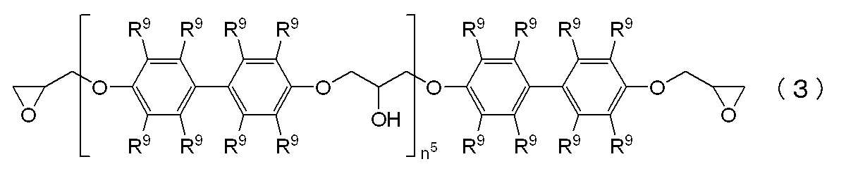
式(3)中、複数存在するR9はそれぞれ独立に水素原子又は炭素数1~4の炭化水素基を表し、n5は重合度を表し、その平均値は0~4の整数である。
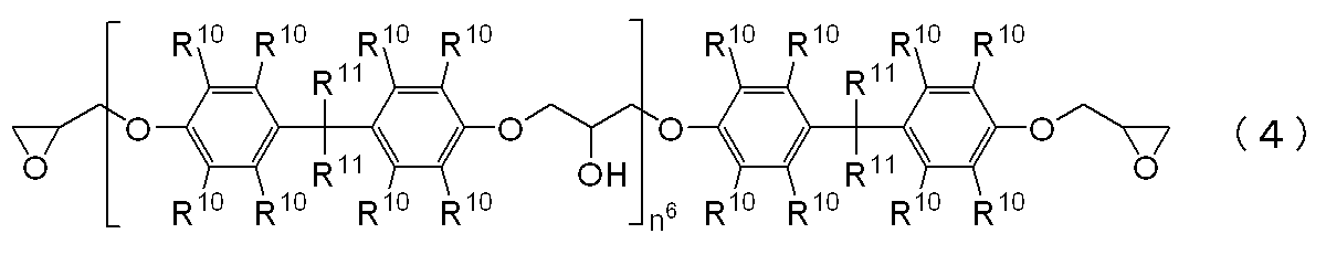
式(4)中、複数存在するR10及びR11はそれぞれ独立に水素原子又は炭素数1~4の炭化水素基を表し、n6は重合度を表し、その平均値は0~4の整数である。
(A)エポキシ樹脂の含有量は、エポキシ樹脂組成物全体に対して、3質量%以上であることが好ましく、5質量%以上であることがより好ましい。こうすることで、粘度上昇によるワイヤ切れを引き起こす恐れを少なくすることができる。また、エポキシ樹脂(A)の含有量は、エポキシ樹脂組成物全体に対して、18質量%以下であることが好ましく、13質量%以下であることがより好ましく、11質量%以下がさらに好ましい。こうすることで、吸水率増加による耐湿信頼性の低下等を引き起こす恐れを少なくすることができる。
(B)硬化剤としては、例えば重付加型の硬化剤、触媒型の硬化剤、縮合型の硬化剤の3タイプに大別することができる。
重付加型の硬化剤としては、例えば、ジエチレントリアミン(DETA)、トリエチレンテトラミン(TETA)、メタキシレリレンジアミン(MXDA)などの脂肪族ポリアミン、ジアミノジフェニルメタン(DDM)、m-フェニレンジアミン(MPDA)、ジアミノジフェニルスルホン(DDS)などの芳香族ポリアミンのほか、ジシアンジアミド(DICY)、有機酸ジヒドララジドなどを含むポリアミン化合物;ヘキサヒドロ無水フタル酸(HHPA)、メチルテトラヒドロ無水フタル酸(MTHPA)などの脂環族酸無水物、無水トリメリット酸(TMA)、無水ピロメリット酸(PMDA)、ベンゾフェノンテトラカルボン酸(BTDA)などの芳香族酸無水物などを含む酸無水物;ノボラック型フェノール樹脂、ポリビニルフェノールなどのフェノール樹脂系硬化剤;ポリサルファイド、チオエステル、チオエーテルなどのポリメルカプタン化合物;イソシアネートプレポリマー、ブロック化イソシアネートなどのイソシアネート化合物;カルボン酸含有ポリエステル樹脂などの有機酸類などが挙げられる。
触媒型の硬化剤としては、例えば、ベンジルジメチルアミン(BDMA)、2,4,6-トリスジメチルアミノメチルフェノール(DMP-30)などの3級アミン化合物;2-メチルイミダゾール、2-エチル-4-メチルイミダゾール(EMI24)などのイミダゾール化合物;BF3錯体などのルイス酸などが挙げられる。
縮合型の硬化剤としては、例えば、レゾール型フェノール樹脂;メチロール基含有尿素樹脂のような尿素樹脂;メチロール基含有メラミン樹脂のようなメラミン樹脂などが挙げられる。
これらの中でも、耐燃性、耐湿性、電気特性、硬化性、保存安定性等のバランスの点からフェノール樹脂系硬化剤が好ましい。フェノール樹脂系硬化剤は、一分子内にフェノール性水酸基を2個以上有するモノマー、オリゴマー、ポリマー全般であり、その分子量、分子構造を特に限定するものではないが、例えば、フェノールノボラック樹脂、クレゾールノボラック樹脂、ビスフェノールノボラック等のノボラック型樹脂;トリフェノールメタン型フェノール樹脂等の多官能型フェノール樹脂;テルペン変性フェノール樹脂、ジシクロペンタジエン変性フェノール樹脂等の変性フェノール樹脂;フェニレン骨格及び/又はビフェニレン骨格を有するフェノールアラルキル樹脂、フェニレン及び/又はビフェニレン骨格を有するナフトールアラルキル樹脂等のアラルキル型樹脂;ビスフェノールA、ビスフェノールF等のビスフェノール化合物等が挙げられ、これらは1種類を単独で用いても2種類以上を併用してもよい。
好ましくは、(B)硬化剤として、下記式(5)で表される化合物からなる群から選択される少なくとも1種の硬化剤を用いることができる。
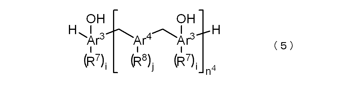
式(5)中、Ar3はフェニレン基又はナフチレン基を表し、Ar3がナフチレン基の場合、水酸基はα位、β位のいずれに結合していてもよく、Ar4はフェニレン基、ビフェニレン基及びナフチレン基のうちのいずれか1つの基を表し、R7及びR8はそれぞれ独立に炭素数1~10の炭化水素基を表し、iは0~5の整数であり、jは0~8の整数であり、n4は重合度を表し、その平均値は1~3の整数である。
(B)硬化剤の含有量は、エポキシ樹脂組成物中に、2質量%以上であることが好ましく、3質量%以上であることがより好ましく、4質量%以上であることがさらに好ましい。こうすることで、充分な流動性を得ることができる。また、(B)硬化剤の含有量は、エポキシ樹脂組成物中に、15質量%以下であることが好ましく、11質量%以下であることがより好ましく、8質量%以下であることがさらに好ましい。こうすることで、吸水率増加による耐湿信頼性の低下等を引き起こす恐れを少なくすることができる。
また、(B)硬化剤としてフェノール樹脂系硬化剤を用いる場合におけるエポキシ樹脂とフェノール樹脂系硬化剤との配合比率としては、全エポキシ樹脂のエポキシ基数(EP)と全フェノール樹脂系硬化剤のフェノール性水酸基数(OH)との当量比(EP)/(OH)が0.8~1.3であることが好ましい。当量比がこの範囲であると、エポキシ樹脂組成物の硬化性の低下、又は樹脂硬化物の物性の低下等を引き起こす恐れが少ない。
(C)炭酸型層状複水酸化物粒子(以下、「炭酸型LDH粒子」ともいう。)は、下記式(1)で表される化合物である。
M1 aM2 b(OH)c(CO3)d・nH2O (1)
〔式(1)中、M1は、Ni2+、Ba2+、Ca2+、Mn2+、Sr2+、Zn2+、Mg2+及びCu2+から選択される二価金属イオンであり、M2はCo3+、Cr3+、Mn3+及びAl3+から選択される三価金属イオンであり、a、b、c、dは、それぞれ1≦a≦8、1≦b≦14、1≦c≦20、1≦d≦12、を満たす整数であり、nは1≦n≦10を満たす整数である。ただし、M1がMg2+のとき、M2がAl3+である場合を除く。〕
M1 aM2 b(OH)c(CO3)d・nH2O (1)
〔式(1)中、M1は、Ni2+、Ba2+、Ca2+、Mn2+、Sr2+、Zn2+、Mg2+及びCu2+から選択される二価金属イオンであり、M2はCo3+、Cr3+、Mn3+及びAl3+から選択される三価金属イオンであり、a、b、c、dは、それぞれ1≦a≦8、1≦b≦14、1≦c≦20、1≦d≦12、を満たす整数であり、nは1≦n≦10を満たす整数である。ただし、M1がMg2+のとき、M2がAl3+である場合を除く。〕
前記式(1)の化合物の中でも、体積頻度粒度分布におけるモード径(最頻値)が0.01μm以上1.0μm以下の範囲にあるものが好ましく、0.05μm以上0.5μm以下の範囲にあるものがより好ましい。モード径がこの範囲にある炭酸型LDH粒子を用いることで、エポキシ樹脂組成物における炭酸型LDH粒子の分布が均一となるため、エポキシ樹脂から発生する酸性イオンや酸化物イオンを炭酸型LDH粒子により確実にトラップして中和することができる。
なお、(C)炭酸型LDH粒子のモード径は、体積頻度粒度分布で表した際の、その頻度値が最大となっている粒径(最頻値径)であり、例えば、レーザー回折散乱式粒度分布測定装置等を用いて測定することができる。
なお、(C)炭酸型LDH粒子のモード径は、体積頻度粒度分布で表した際の、その頻度値が最大となっている粒径(最頻値径)であり、例えば、レーザー回折散乱式粒度分布測定装置等を用いて測定することができる。
(C)炭酸型LDH粒子は、上記式(1)中、M1が、Ni2+、Ba2+、及びCa2+から選択される二価金属イオンであることが好ましく、M2が、Co3+及びAl3+から選択される三価金属イオンであることがより好ましく、M2が、Co3+の三価金属イオンであるか、またはM1が、Ni2+であることがさらに好ましく、M1が、Ni2+であり、かつM2が、Co3+の三価金属イオンである場合が最も好ましい。
本発明において(C)炭酸型LDH粒子は、天然物であっても合成物であってもよく、結晶水を脱水したものであってもよい。天然物の具体例としては、Comblainite(Ni6Co2(OH)16(CO3)・nH2O)、Takovite(Ni6Al2(OH)16(CO3)・nH2O)、Dresserite(BaAl2(OH)4(CO3)2・nH2O)、Almohydrocalcite(CaAl2(OH)4(CO3)2・nH2O)、Stichtite(Mg6Cr2(OH)16(CO3)・nH2O)、Desautelsite(Mg6Mn2(OH)16CO3・nH2O)等が挙げられる。式(1)中のnは1以上10以下であればよいが、1以上8以下が好ましく、2以上8以下がより好ましい。また、式(1)中のbは1以上14以下であればよいが、1以上4以下が好ましく、dは1以上12以下であればよいが、1以上4以下が好ましい。
炭酸型LDH粒子は次のようにして合成される。金属の塩、例えば硝酸塩の水溶液を水酸化ナトリウム、炭酸ナトリウムの水溶液に攪拌しながら室温で添加する。生成した沈殿物を60~200℃で数時間加熱して結晶化させる。洗浄及び乾燥により層状複水酸化物の炭酸塩を含む無機化合物が得られる。
炭酸型LDH粒子は次のようにして合成される。金属の塩、例えば硝酸塩の水溶液を水酸化ナトリウム、炭酸ナトリウムの水溶液に攪拌しながら室温で添加する。生成した沈殿物を60~200℃で数時間加熱して結晶化させる。洗浄及び乾燥により層状複水酸化物の炭酸塩を含む無機化合物が得られる。
(C)炭酸型LDH粒子の含有量としては、エポキシ樹脂組成物全体に対して0.01~10質量%が好ましく、0.05~2質量%であることがより好ましい。(C)炭酸型LDH粒子の含有量を、好ましくは0.01質量%以上、より好ましくは0.05質量%以上とすることで、pH調整剤の効果を十分に発揮させることができ、金属ワイヤと電極パッドとのボンディング部の腐食(酸化劣化)をより確実に防止することができる。また、(C)炭酸型LDH粒子の含有量を、好ましくは10質量%以下、より好ましくは2質量%以下とすることで、吸湿率を低下させることができる。したがって、(C)炭酸型LDH粒子の含有量を上記範囲とすることで、ボンディング部の断線をよりいっそう確実に抑制することができる。
また、本発明のエポキシ樹脂組成物は、(D)充填材、及び必要に応じて(E)硬化促進剤を含んでいてもよい。
(D)充填材としては、一般の半導体封止用エポキシ樹脂組成物に使用されているものを用いることができる。例えば、溶融球状シリカ、溶融破砕シリカ、結晶シリカ、タルク、アルミナ、チタンホワイト、窒化珪素等の無機充填材、オルガノシリコーンパウダー、ポリエチレンパウダー等の有機充填材が挙げられ、中でも、溶融球状シリカが特に好ましい。これらの充填材は、1種を単独で用いても2種以上を併用しても差し支えない。また、(D)充填材の形状としては、エポキシ樹脂組成物の溶融粘度の上昇を抑え、更に充填材の含有量を高めるためには、できるだけ真球状であり、かつ粒度分布がブロードであることが好ましい。また、充填材がカップリング剤により表面処理されていてもかまわない。さらに、必要に応じて充填材をエポキシ樹脂又はフェノール樹脂等で予め処理して用いてもよく、処理の方法としては、溶媒を用いて混合した後に溶媒を除去する方法や、直接充填材に添加し、混合機を用いて混合処理する方法等がある。
(D)充填材の含有量は、エポキシ樹脂組成物の充填性、半導体装置の信頼性の観点から、エポキシ樹脂組成物全体に対して、65質量%以上であることが好ましく、75質量%以上であることがより好ましく、80質量%以上がさらに好ましい。こうすることで、低吸湿性、低熱膨張性が得られるため耐湿信頼性が不十分となる恐れを少なくすることができる。また、(D)充填材の含有量は、成形性を考慮すると、エポキシ樹脂組成物全体に対して、93質量%以下であることが好ましく、91質量%以下であることがより好ましく、90質量%以下がさらに好ましい。こうすることで、流動性が低下し成形時に充填不良等が生じたり、高粘度化による半導体装置内のワイヤ流れ等の不都合が生じたりする恐れを少なくすることができる。
(E)硬化促進剤は、エポキシ樹脂のエポキシ基と硬化剤(たとえば、フェノール樹脂系硬化剤のフェノール性水酸基)との架橋反応を促進させるものであればよく、一般の半導体封止用エポキシ樹脂組成物に使用するものを用いることができる。例えば、1,8-ジアザビシクロ(5,4,0)ウンデセン-7等のジアザビシクロアルケン及びその誘導体;トリフェニルホスフィン、メチルジフェニルホスフィン等の有機ホスフィン類;2-メチルイミダゾール等のイミダゾール化合物;テトラフェニルホスホニウム・テトラフェニルボレート等のテトラ置換ホスホニウム・テトラ置換ボレート;ホスフィン化合物とキノン化合物との付加物等が挙げられ、これらは1種類を単独で用いても2種以上を併用しても差し支えない。
(E)硬化促進剤の含有量は、エポキシ樹脂組成物全体に対して、0.05質量%以上であることが好ましく、0.1質量%以上であることがより好ましい。こうすることで、硬化性の低下を引き起こす恐れを少なくすることができる。また、(E)硬化促進剤の含有量は、エポキシ樹脂組成物全体に対して、1質量%以下であることが好ましく、0.5質量%以下であることがより好ましい。こうすることで、流動性の低下を引き起こす恐れを少なくすることができる。
エポキシ樹脂組成物には、さらに必要に応じて、炭酸カルシウム、硼酸カルシウム、メタケイ酸カルシウム、水酸化アルミニウム、ベーマイト等の中和剤、水酸化ジルコニウム等のアルミニウム腐食防止剤;酸化ビスマス水和物等の無機イオン交換体;エポキシシラン、γ-グリシドキシプロピルトリメトキシシラン、3-メルカプトプロピルトリメトキシシラン、3-アミノプロピルトリメトキシシラン等のカップリング剤;カーボンブラック、ベンガラ等の着色剤;シリコーンゴム等の低応力成分;カルナバワックス等の天然ワックス、合成ワックス、ステアリン酸亜鉛等の高級脂肪酸及びその金属塩類もしくはパラフィン等の離型剤;水酸化アルミニウム、水酸化マグネシウム、ホウ酸亜鉛、モリブデン酸亜鉛、ホスファゼン等の難燃剤、酸化防止剤等の各種添加剤を適宜配合してもよい。
エポキシ樹脂組成物は、前述の各成分を、例えば、ミキサー等を用いて15℃~28℃で混合したもの、さらにその後、ロール、ニーダー、押出機等の混練機で溶融混練し、冷却後粉砕したものなど、必要に応じて適宜分散度や流動性等を調整したものを用いることができる。
本発明の半導体封止用エポキシ樹脂組成物の硬化体は、上記のエポキシ樹脂組成物をトランスファーモールド、コンプレッションモールド、インジェクションモールド等の従来からの成形方法で成形硬化して得ることができる。トランスファーモールドなどの成形方法で成形硬化されたエポキシ樹脂組成物の硬化体は、必要に応じて80℃~200℃程度の温度で、10分~24時間程度の時間をかけて完全硬化させることで得ることもできる。
つづいて、本発明の半導体装置について図1を用いつつ説明する。本発明の半導体装置10は、基板として、ダイパッド部3aと、インナーリード部3bを有するリードフレーム3を備え、ダイパッド部3aに搭載された半導体素子1と、リードフレーム3と半導体素子1とを電気的に接続している金属ワイヤ4と、上記のエポキシ樹脂組成物の硬化体からなり、半導体素子1と金属ワイヤ4とを封止している、封止樹脂5と、を有する。
半導体素子1としては、特に限定されるものではなく、例えば、集積回路、大規模集積回路、固体撮像素子等が挙げられる。
リードフレーム3としては特に制限はなく、リードフレーム3に代えて回路基板を用いてもよい。具体的には、デュアル・インライン・パッケージ(DIP)、プラスチック・リード付きチップ・キャリア(PLCC)、クワッド・フラット・パッケージ(QFP)、ロー・プロファイル・クワッド・フラット・パッケージ(LQFP)、スモール・アウトライン・Jリード・パッケージ(SOJ)、薄型スモール・アウトライン・パッケージ(TSOP)、薄型クワッド・フラット・パッケージ(TQFP)、テープ・キャリア・パッケージ(TCP)、ボール・グリッド・アレイ(BGA)、チップ・サイズ・パッケージ(CSP)、クワッド・フラット・ノンリーデッド・パッケージ(QFN)、スモールアウトライン・ノンリーデッド・パッケージ(SON)、リードフレーム・BGA(LF-BGA)、モールド・アレイ・パッケージタイプのBGA(MAP-BGA)などの従来公知の半導体装置に用いられるリードフレーム又は回路基板を用いることができる。
半導体素子1は、複数の半導体素子が積層されたものであってもよい。この場合、1段目の半導体素子はフィルム接着剤、熱硬化性接着剤等のダイボンド材硬化体2を介してダイパッド部3aに接着される。2段目以降の半導体素子は絶縁性のフィルム接着剤により順次積層させることができる。そして、各層の適切な場所に、予め前工程で電極パッド6が形成されている。
電極パッド6は、アルミニウム(Al)を主成分とするものからなることが好ましい。電極パッド6中のAlの含有量は、電極パッド6全体に対して98質量%以上が好ましい。電極パッド6中に含まれるAl以外の成分としては、銅(Cu)、シリコン(Si)等が挙げられる。電極パッド6は、下層の銅回路端子の表面に一般的なチタン系バリア層を形成し、さらにAlを蒸着、スパッタリング、無電解メッキなど、一般的な半導体素子の電極パッドの形成方法を適用することにより作製することができる。
金属ワイヤ4は、リードフレーム3と、リードフレーム3のダイパッド部3aに搭載された半導体素子1とを電気的に接続するために使用される。金属ワイヤ4の表面には、自然に又はプロセス上不可避的に酸化膜が形成されていてもよい。本発明において、金属ワイヤ4とは、このようにワイヤ表面に形成された酸化膜を具備するものも含まれる。
金属ワイヤ4のワイヤ径は、30μm以下、さらに好ましくは25μm以下でありかつ15μm以上であることが好ましい。この範囲であれば金属ワイヤ先端のボール形状が安定し、ボンディング部の接続信頼性を向上させることができる。また、金属ワイヤ自身の硬さによりワイヤ流れを低減することが可能となる。
金属ワイヤ4は、限定されず、金ワイヤ、銅ワイヤのいずれであってもよいが、銅ワイヤであることが好ましく、金属ワイヤ4中の銅の含有量は、金属ワイヤ4全体に対して、99.9~100質量%であることが好ましく、99.99~99.999質量%であることがより好ましい。銅の含有量が金属ワイヤ全体に対して99.99質量%以上の金属ワイヤ4であれば、ボール部分が充分な柔軟性を有しているため、ボンディング時にパッド側にダメージを与えるおそれがなく、特に好ましい。尚、本発明の半導体装置で用いることができる金属ワイヤ4は、芯線である銅にBa、Ca、Sr、Be、Al又は希土類金属を0.001~0.1質量%ドープすることでさらにボール形状と接合強度を改善させることができる。
銅ワイヤ4と電極パッド6との接合部において、銅ワイヤ4の先端には、ボール4aが形成されている。
また、金属ワイヤ4が銅ワイヤである場合は、その表面にパラジウムを含む金属材料で構成された被覆層を有していてもよい。これにより、銅ワイヤ先端のボール形状が安定し、ボンディング部の接続信頼性を向上させることができる。また、芯線である銅の酸化劣化を防止する効果も得られ、ボンディング部の高温耐湿性を向上させることができる。
銅ワイヤにおけるパラジウムを含む金属材料から構成された被覆層の厚みとしては、0.001~0.02μmであることが好ましく、0.005~0.015μmであることがより好ましい。上記上限値以下であると、ワイヤボンド時に芯線である銅と被覆材のパラジウムを含む金属材料とが十分に溶けて安定なボール形状を形成させることができ、ボンディング部の高温耐湿性をよりいっそう向上させることができる。また、上記下限値以上であると、芯線の銅の酸化劣化を防止でき、同様にボンディング部の高温耐湿性を更に向上させることができる。
銅ワイヤは、銅合金を溶解炉で鋳造し、その鋳塊をロール圧延し、さらにダイスを用いて伸線加工を行い、連続的にワイヤを掃引しながら加熱する後熱処理を施して得ることができる。また、半導体装置10で用いることができる銅ワイヤにおけるパラジウムを含む金属材料から構成された被覆層は、予め狙いのワイヤ径の線を準備し、これを、パラジウムを含む電解溶液又は無電解溶液に浸漬し、連続的に掃引してメッキすることで被覆層を形成することができる。この場合、被覆の厚さは掃引速度で調整することができる。また、狙いよりも太い線を準備して、これを電解溶液又は無電解溶液に浸漬し連続的に掃引して被覆層を形成し、さらに所定の径になるまで伸線する手法も取れる。
つづいて、半導体装置10の製造方法の一例について説明する。
まず、公知の半導体製造プロセスによって半導体素子1の最上層の保護膜8の一部を開口して電極パッド6を形成する。保護膜8はSiN等の絶縁膜から形成される。次いで、更に公知の後工程プロセスにより電極パッド6を備えた半導体素子1をリードフレーム3上のダイパッド部3aに設置し、金属ワイヤ4により電極パッド6とインナーリード部3bとをワイヤボンディングする。
まず、公知の半導体製造プロセスによって半導体素子1の最上層の保護膜8の一部を開口して電極パッド6を形成する。保護膜8はSiN等の絶縁膜から形成される。次いで、更に公知の後工程プロセスにより電極パッド6を備えた半導体素子1をリードフレーム3上のダイパッド部3aに設置し、金属ワイヤ4により電極パッド6とインナーリード部3bとをワイヤボンディングする。
ボンディングは、たとえば以下の手順で行う。まず、金属ワイヤ4の先端に所定の径のボール4aを形成する。ついで、ボール4aを電極パッド6上面に対して実質的に垂直に降下させ、ボール4aと電極パッド6とを接触させながら、超音波振動を与える。これにより、ボール4aの底部が電極パッド6に接触して接合面が形成される。
なお、リードフレーム3のリード部3bと半導体素子1とは、ワイヤのリバースボンドで接合されていてもよい。リバースボンドでは、まず半導体素子1の電極パッド6に銅ワイヤ4の先端に形成されたボールを接合し、銅ワイヤ4を切断してステッチ接合用のバンプを形成する。次にリードフレーム3の金属メッキされたリード部3bに対してワイヤの先端に形成されたボールを接合し、半導体素子のバンプにステッチ接合する。リバースボンドでは正ボンディングより半導体素子1上のワイヤ高さを低くすることができるため、半導体素子1の接合高さを低くすることができる。
次いで、本発明の半導体封止用エポキシ樹脂組成物を用いて、半導体素子1等の電子部品を封止し、トランスファーモールド、コンプレッションモールド、インジェクションモールド等の従来からの成形方法で硬化成形して得られる。トランスファーモールドなどの成形方法で封止された半導体装置は、そのまま、或いは80℃~200℃程度の温度で、10分~24時間程度の時間をかけて完全硬化させた後、電子機器等に搭載される。
このように製造された半導体装置10では、製造プロセスや使用時にボンディング部に熱がかかると、金属ワイヤ4から金属が電極パッド6に拡散してワイヤとパッドとの接合部に合金層が形成されるが、エポキシ樹脂から発生する酸性成分や酸化物成分は、合金層に到達する前に、炭酸型層状複水酸化物粒子にトラップされて中和することができるため、ボンディング部の腐食(酸化)による断線を防止することができる。したがって、本発明によれば、ボンディング後に高温高湿プロセスを採用する場合や、使用環境が高温高湿下である場合(例えば、自動車などのエンジン周辺に設置される場合)においても、高い接続信頼性を維持することが可能である。
以上、図面を参照して本発明の実施形態について述べたが、これらは本発明の例示であり、上記以外の様々な構成を採用することもできる。
以下、実施例及び比較例に基づいて本発明をより具体的に説明するが、本発明は以下の実施例に限定されるものではない。
実施例1~4、比較例1~3
ミキサーを用いて表1に示す各成分を15~28℃で混合し、次いで70℃~100℃でロール混練した。冷却後、粉砕してエポキシ樹脂組成物を得た。なお、表1中、各成分の詳細は下記のとおりである。また、表1中の単位は、質量%である。
ミキサーを用いて表1に示す各成分を15~28℃で混合し、次いで70℃~100℃でロール混練した。冷却後、粉砕してエポキシ樹脂組成物を得た。なお、表1中、各成分の詳細は下記のとおりである。また、表1中の単位は、質量%である。
<(A)エポキシ樹脂>
エポキシ-OCN:EOCN-1020-55、日本化薬株式会社製、エポキシ当量200
エポキシ-Biphenyl:YX4000K、三菱化学株式会社製、エポキシ当量185
エポキシ-BA:NC3000P、日本化薬株式会社製、エポキシ当量276
エポキシ-OCN:EOCN-1020-55、日本化薬株式会社製、エポキシ当量200
エポキシ-Biphenyl:YX4000K、三菱化学株式会社製、エポキシ当量185
エポキシ-BA:NC3000P、日本化薬株式会社製、エポキシ当量276
<(B)硬化剤>
硬化剤-PN:PR-HF-3、住友ベークライト株式会社製、水酸基当量105
硬化剤-XL:XLC-4L、三井化学株式会社製、水酸基当量168
硬化剤-BA:MEH-7851SS、明和化成株式会社製、水酸基当量203
硬化剤-PN:PR-HF-3、住友ベークライト株式会社製、水酸基当量105
硬化剤-XL:XLC-4L、三井化学株式会社製、水酸基当量168
硬化剤-BA:MEH-7851SS、明和化成株式会社製、水酸基当量203
<(C)炭酸型LDH粒子>
表1中成分(C)は下記の方法で製造した。なお、化学分析は、金属元素については、得られた結晶を硝酸水溶液に溶かしイオンクロマトグラフィーで定量することにより行い、その他の元素についてはTGDTA(熱重量測定-示差熱分析)で定量することによって行った。モード径は、株式会社島津製作所製レーザー回折散乱式粒度分布計SALD-7000を使用して測定した。
表1中成分(C)は下記の方法で製造した。なお、化学分析は、金属元素については、得られた結晶を硝酸水溶液に溶かしイオンクロマトグラフィーで定量することにより行い、その他の元素についてはTGDTA(熱重量測定-示差熱分析)で定量することによって行った。モード径は、株式会社島津製作所製レーザー回折散乱式粒度分布計SALD-7000を使用して測定した。
CI-1:Comblainite(Ni6Co2(OH)16(CO3)・4H2O)の合成
Ni(NO3)2・6H2O、40gとCo(NO3)2・6H2O、15gを200mlのイオン交換水に溶解した。これを4Nの水酸化ナトリウム水溶液200mlに無水炭酸ナトリウム10gを溶解した水溶液によく攪拌しながら室温でゆっくりと加えた。これを90℃12時間で加熱処理した後、室温まで放冷し、沈殿物をろ過した。得られた結晶をイオン交換水で洗浄し、200℃8時間で乾燥させた。化学分析で求めた化学式はNi6Co2(OH)16(CO3)・4H2Oであり、収量は16.5g、モード径は0.12μmであった。
Ni(NO3)2・6H2O、40gとCo(NO3)2・6H2O、15gを200mlのイオン交換水に溶解した。これを4Nの水酸化ナトリウム水溶液200mlに無水炭酸ナトリウム10gを溶解した水溶液によく攪拌しながら室温でゆっくりと加えた。これを90℃12時間で加熱処理した後、室温まで放冷し、沈殿物をろ過した。得られた結晶をイオン交換水で洗浄し、200℃8時間で乾燥させた。化学分析で求めた化学式はNi6Co2(OH)16(CO3)・4H2Oであり、収量は16.5g、モード径は0.12μmであった。
CI-2:Takovite(Ni6Al2(OH)16(CO3)・4H2O)の合成
Ni(NO3)2・6H2O、60gとAl(NO3)3・9H2O、20gを200mlのイオン交換水に溶解した。これを4Nの水酸化ナトリウム水溶液200mlに無水炭酸ナトリウム10gを溶解した水溶液によく攪拌しながら室温でゆっくりと加えた。これを90℃12時間で加熱処理した後、室温まで放冷し、沈殿物をろ過した。得られた結晶をイオン交換水で洗浄し、200℃8時間で乾燥させた。化学分析で求めた化学式はNi6Al2(OH)16(CO3)・4H2Oであり、収量は14.1g、モード径は0.09μmであった。
Ni(NO3)2・6H2O、60gとAl(NO3)3・9H2O、20gを200mlのイオン交換水に溶解した。これを4Nの水酸化ナトリウム水溶液200mlに無水炭酸ナトリウム10gを溶解した水溶液によく攪拌しながら室温でゆっくりと加えた。これを90℃12時間で加熱処理した後、室温まで放冷し、沈殿物をろ過した。得られた結晶をイオン交換水で洗浄し、200℃8時間で乾燥させた。化学分析で求めた化学式はNi6Al2(OH)16(CO3)・4H2Oであり、収量は14.1g、モード径は0.09μmであった。
CI-3:Dresserite(BaAl2(OH)4(CO3)2・H2O)の合成
Ba(NO3)2、13gとAl(NO3)3・9H2O、40gを200mlのイオン交換水に溶解した。これを4Nの水酸化ナトリウム水溶液200mlに無水炭酸ナトリウム10gを溶解した水溶液によく攪拌しながら室温でゆっくりと加えた。これを90℃12時間で加熱処理した後、室温まで放冷し、沈殿物をろ過した。得られた結晶をイオン交換水で洗浄し、200℃8時間で乾燥させた。化学分析で求めた化学式はBaAl2(OH)4(CO3)2・H2Oであり、収量は15.3g、モード径は0.18μmであった。
Ba(NO3)2、13gとAl(NO3)3・9H2O、40gを200mlのイオン交換水に溶解した。これを4Nの水酸化ナトリウム水溶液200mlに無水炭酸ナトリウム10gを溶解した水溶液によく攪拌しながら室温でゆっくりと加えた。これを90℃12時間で加熱処理した後、室温まで放冷し、沈殿物をろ過した。得られた結晶をイオン交換水で洗浄し、200℃8時間で乾燥させた。化学分析で求めた化学式はBaAl2(OH)4(CO3)2・H2Oであり、収量は15.3g、モード径は0.18μmであった。
CI-4:Almohydrocalcite(CaAl2(OH)4(CO3)2・2H2O)の合成
Ca(NO3)2・4H2O、12gとAl(NO3)3・9H2O、40gを200mlのイオン交換水に溶解した。これを4Nの水酸化ナトリウム水溶液200mlに無水炭酸ナトリウム10gを溶解した水溶液によく攪拌しながら室温でゆっくりと加えた。これを90℃12時間で加熱処理した後、室温まで放冷し、沈殿物をろ過した。得られた結晶をイオン交換水で洗浄し、200℃8時間で乾燥させた。化学分析で求めた化学式はCaAl2(OH)4(CO3)2・2H2Oであり、収量は14.2g、モード径は0.23μmであった。
Ca(NO3)2・4H2O、12gとAl(NO3)3・9H2O、40gを200mlのイオン交換水に溶解した。これを4Nの水酸化ナトリウム水溶液200mlに無水炭酸ナトリウム10gを溶解した水溶液によく攪拌しながら室温でゆっくりと加えた。これを90℃12時間で加熱処理した後、室温まで放冷し、沈殿物をろ過した。得られた結晶をイオン交換水で洗浄し、200℃8時間で乾燥させた。化学分析で求めた化学式はCaAl2(OH)4(CO3)2・2H2Oであり、収量は14.2g、モード径は0.23μmであった。
CI-5:協和化学工業株式会社DHT-4C(Mg7.2Al3.3(OH)26.3(CO3)mH2O)。モード径は0.21μmである。
<(D)充填材>
シリカ:FB-820、電気化学工業株式会社社製、溶融球状シリカ、平均粒径26.5μm、105μm以上の粒子1%以下
シリカ:FB-820、電気化学工業株式会社社製、溶融球状シリカ、平均粒径26.5μm、105μm以上の粒子1%以下
<(E)硬化促進剤>
トリフェニルホスフィン(TPP)、北興化学工業株式会社製
トリフェニルホスフィン(TPP)、北興化学工業株式会社製
<その他の成分>
カップリング剤:エポキシシラン
着色剤:カーボンブラック
離型剤:カルナバワックス
カップリング剤:エポキシシラン
着色剤:カーボンブラック
離型剤:カルナバワックス
実施例1~4、比較例1~3のエポキシ樹脂組成物の物性を以下の方法により測定した。その結果を表1に示す。
<スパイラルフロー(SF)>
低圧トランスファー成形機(コータキ精機株式会社製「KTS-15」)を用いて、EMMI-1-66に準じたスパイラルフロー測定用の金型に、金型温度175℃、注入圧力6.9MPa、硬化時間120秒の条件で、実施例1~4、比較例1~3のエポキシ樹脂組成物をそれぞれ注入し、流動長(単位:cm)を測定した。
低圧トランスファー成形機(コータキ精機株式会社製「KTS-15」)を用いて、EMMI-1-66に準じたスパイラルフロー測定用の金型に、金型温度175℃、注入圧力6.9MPa、硬化時間120秒の条件で、実施例1~4、比較例1~3のエポキシ樹脂組成物をそれぞれ注入し、流動長(単位:cm)を測定した。
<ゲルタイム(GT)>
175℃に加熱した熱板上で実施例1~4、比較例1~3のエポキシ樹脂組成物をそれぞれ溶融後、へらで練りながら硬化するまでの時間(単位:秒)を測定した。
175℃に加熱した熱板上で実施例1~4、比較例1~3のエポキシ樹脂組成物をそれぞれ溶融後、へらで練りながら硬化するまでの時間(単位:秒)を測定した。
<耐湿性(HAST)>
アルミニウム製電極パッド(アルミニウム純度99.9質量%、厚み1μm)を備えるTEG(TEST ELEMENT GROUP)チップ(3.5mm×3.5mm)を352ピンBGA(基板は厚さ0.56mm、ビスマレイミド・トリアジン樹脂/ガラスクロス基板、パッケージサイズは30mm×30mm、厚さ1.17mm)のダイパッド部に接着し、TEGチップの電極パッドと基板の電極パッドとをデイジーチェーン接続となるように、銅ワイヤ(銅純度99.99質量%、径25μm)を用いてワイヤピッチ80μmでワイヤボンディングした。これを、低圧トランスファー成形機(TOWA製「Yシリーズ」)を用いて、金型温度175℃、注入圧力6.9MPa、硬化時間2分の条件で、実施例1~4、比較例1~3のエポキシ樹脂組成物を用いて封止成形して、352ピンBGAパッケージを作製した。このパッケージを175℃、4時間の条件で後硬化した後、半導体装置を得た。得られた半導体装置について半導体装置のHAST(耐湿性試験)を行った。具体的には、IEC68-2-66に準拠して実施した。試験条件は、温度を130℃、および140℃とし、85%RH、印加電圧20Vで処理し、不良が発生する時間を調べた。なお、不良の判定は、作製したパッケージ10個を用いて評価し、初期抵抗に対する処理後の抵抗値が1.2倍を超えたパッケージが発生した時間を不良時間とした。その結果を表1に示す。表1中単位は、時間(hour)である。
アルミニウム製電極パッド(アルミニウム純度99.9質量%、厚み1μm)を備えるTEG(TEST ELEMENT GROUP)チップ(3.5mm×3.5mm)を352ピンBGA(基板は厚さ0.56mm、ビスマレイミド・トリアジン樹脂/ガラスクロス基板、パッケージサイズは30mm×30mm、厚さ1.17mm)のダイパッド部に接着し、TEGチップの電極パッドと基板の電極パッドとをデイジーチェーン接続となるように、銅ワイヤ(銅純度99.99質量%、径25μm)を用いてワイヤピッチ80μmでワイヤボンディングした。これを、低圧トランスファー成形機(TOWA製「Yシリーズ」)を用いて、金型温度175℃、注入圧力6.9MPa、硬化時間2分の条件で、実施例1~4、比較例1~3のエポキシ樹脂組成物を用いて封止成形して、352ピンBGAパッケージを作製した。このパッケージを175℃、4時間の条件で後硬化した後、半導体装置を得た。得られた半導体装置について半導体装置のHAST(耐湿性試験)を行った。具体的には、IEC68-2-66に準拠して実施した。試験条件は、温度を130℃、および140℃とし、85%RH、印加電圧20Vで処理し、不良が発生する時間を調べた。なお、不良の判定は、作製したパッケージ10個を用いて評価し、初期抵抗に対する処理後の抵抗値が1.2倍を超えたパッケージが発生した時間を不良時間とした。その結果を表1に示す。表1中単位は、時間(hour)である。

また、炭酸型LDH粒子において、Mn2+、Sr2+、Zn2+及びCu2+から選択される二価金属イオンと、Cr3+及びMn3+から選択される三価金属イオンとを用いた場合においても、上記実施例と同様にして、良好な結果が得られた。また上記実施例で用いたNi2+、Ba2+、Ca2+及びMg2+と、Co3+及びAl3+との組み合わせ以外の組み合わせによる炭酸型LDH粒子を用いた場合も、同様にして、良好な結果が得られた。
この出願は、2012年3月30日に出願された日本特許出願特願2012-079092を基礎とする優先権を主張し、その開示の全てをここに取り込む。
Claims (10)
- 金属ワイヤ及び前記金属ワイヤが接続された半導体素子を封止するために用いられる半導体封止用エポキシ樹脂組成物であって、
下記成分
(A)エポキシ樹脂
(B)硬化剤
(C)下記式(1)で表される炭酸型層状複水酸化物粒子
を含む、半導体封止用エポキシ樹脂組成物。
M1 aM2 b(OH)c(CO3)d・nH2O (1)
〔式(1)中、M1は、Ni2+、Ba2+、Ca2+、Mn2+、Sr2+、Zn2+、Mg2+及びCu2+から選択される二価金属イオンであり、M2はCo3+、Cr3+、Mn3+及びAl3+から選択される三価金属イオンであり、a、b、c、dは、それぞれ1≦a≦8、1≦b≦14、1≦c≦20、1≦d≦12、を満たす整数であり、nは1≦n≦10を満たす整数である。ただし、M1がMg2+のとき、M2がAl3+である場合を除く。〕 - 前記成分(C)の体積頻度粒度分布におけるモード径が0.01μm以上1.0μm以下の範囲である、請求項1に記載の半導体封止用エポキシ樹脂組成物。
- 前記式(1)中、M1が、Ni2+、Ba2+、及びCa2+から選択される二価金属イオンである、請求項1又は2に記載の半導体封止用エポキシ樹脂組成物。
- 前記式(1)中、M2が、Co3+及びAl3+から選択される三価金属イオンである、請求項1乃至3いずれか一項に記載の半導体封止用エポキシ樹脂組成物。
- 前記金属ワイヤが、銅の含有量が該金属ワイヤ全体に対して99.99質量%以上の銅ワイヤである、請求項1乃至4いずれか一項に記載の半導体封止用エポキシ樹脂組成物。
- 請求項1乃至5いずれか一項に記載の半導体封止用エポキシ樹脂組成物の硬化体。
- 基板に搭載された半導体素子と、
前記半導体素子に設けられた電極パッドと、
前記基板に設けられた接続端子と前記電極パッドとを接続する金属ワイヤと、
請求項6に記載された半導体封止用エポキシ樹脂組成物の硬化体と、
を備える、半導体装置。 - 前記金属ワイヤが銅ワイヤである、請求項7に記載の半導体装置。
- 前記電極パッドがアルミニウムを主成分とする、請求項7又は8に記載の半導体装置。
- 前記基板が、リードフレーム又は回路基板である、請求項7乃至9いずれか一項に記載の半導体装置。
Applications Claiming Priority (2)
| Application Number | Priority Date | Filing Date | Title |
|---|---|---|---|
| JP2012-079092 | 2012-03-30 | ||
| JP2012079092A JP2015110686A (ja) | 2012-03-30 | 2012-03-30 | 半導体封止用エポキシ樹脂組成物、その硬化体及び半導体装置 |
Publications (1)
| Publication Number | Publication Date |
|---|---|
| WO2013145609A1 true WO2013145609A1 (ja) | 2013-10-03 |
Family
ID=49258924
Family Applications (1)
| Application Number | Title | Priority Date | Filing Date |
|---|---|---|---|
| PCT/JP2013/001699 Ceased WO2013145609A1 (ja) | 2012-03-30 | 2013-03-14 | 半導体封止用エポキシ樹脂組成物、その硬化体及び半導体装置 |
Country Status (3)
| Country | Link |
|---|---|
| JP (1) | JP2015110686A (ja) |
| TW (1) | TW201341422A (ja) |
| WO (1) | WO2013145609A1 (ja) |
Citations (3)
| Publication number | Priority date | Publication date | Assignee | Title |
|---|---|---|---|---|
| JP2005001902A (ja) * | 2003-06-09 | 2005-01-06 | Toagosei Co Ltd | 無機陰イオン交換体およびそれを用いた電子部品封止用エポキシ樹脂組成物 |
| JP2009152561A (ja) * | 2007-11-29 | 2009-07-09 | Sumitomo Bakelite Co Ltd | 半導体装置並びに封止用エポキシ樹脂組成物及びその製造方法 |
| JP2009235177A (ja) * | 2008-03-26 | 2009-10-15 | Sumitomo Bakelite Co Ltd | 半導体封止用エポキシ樹脂組成物および半導体装置 |
-
2012
- 2012-03-30 JP JP2012079092A patent/JP2015110686A/ja active Pending
-
2013
- 2013-03-14 WO PCT/JP2013/001699 patent/WO2013145609A1/ja not_active Ceased
- 2013-03-15 TW TW102109330A patent/TW201341422A/zh unknown
Patent Citations (3)
| Publication number | Priority date | Publication date | Assignee | Title |
|---|---|---|---|---|
| JP2005001902A (ja) * | 2003-06-09 | 2005-01-06 | Toagosei Co Ltd | 無機陰イオン交換体およびそれを用いた電子部品封止用エポキシ樹脂組成物 |
| JP2009152561A (ja) * | 2007-11-29 | 2009-07-09 | Sumitomo Bakelite Co Ltd | 半導体装置並びに封止用エポキシ樹脂組成物及びその製造方法 |
| JP2009235177A (ja) * | 2008-03-26 | 2009-10-15 | Sumitomo Bakelite Co Ltd | 半導体封止用エポキシ樹脂組成物および半導体装置 |
Also Published As
| Publication number | Publication date |
|---|---|
| JP2015110686A (ja) | 2015-06-18 |
| TW201341422A (zh) | 2013-10-16 |
Similar Documents
| Publication | Publication Date | Title |
|---|---|---|
| CN102666724B (zh) | 半导体密封用环氧树脂组合物、其固化体及半导体装置 | |
| JP5532258B2 (ja) | 半導体装置 | |
| JP5393207B2 (ja) | 半導体装置 | |
| JP6330658B2 (ja) | 半導体装置 | |
| WO2012070529A1 (ja) | 半導体封止用エポキシ樹脂組成物及び半導体装置 | |
| JP2013209450A (ja) | 半導体封止用エポキシ樹脂組成物 | |
| JP6094573B2 (ja) | 半導体装置 | |
| JP2015017165A (ja) | 封止用エポキシ樹脂組成物、及び半導体装置 | |
| JP6341203B2 (ja) | 半導体装置 | |
| WO2011030516A1 (ja) | 半導体装置 | |
| JP2015110686A (ja) | 半導体封止用エポキシ樹脂組成物、その硬化体及び半導体装置 | |
| JP5125673B2 (ja) | 半導体封止用エポキシ樹脂組成物および半導体装置 |
Legal Events
| Date | Code | Title | Description |
|---|---|---|---|
| 121 | Ep: the epo has been informed by wipo that ep was designated in this application |
Ref document number: 13767970 Country of ref document: EP Kind code of ref document: A1 |
|
| 122 | Ep: pct application non-entry in european phase |
Ref document number: 13767970 Country of ref document: EP Kind code of ref document: A1 |
|
| NENP | Non-entry into the national phase |
Ref country code: DE |
|
| NENP | Non-entry into the national phase |
Ref country code: JP |