WO2013141181A1 - Semiconductor device and semiconductor device manufacturing method - Google Patents
Semiconductor device and semiconductor device manufacturing method Download PDFInfo
- Publication number
- WO2013141181A1 WO2013141181A1 PCT/JP2013/057562 JP2013057562W WO2013141181A1 WO 2013141181 A1 WO2013141181 A1 WO 2013141181A1 JP 2013057562 W JP2013057562 W JP 2013057562W WO 2013141181 A1 WO2013141181 A1 WO 2013141181A1
- Authority
- WO
- WIPO (PCT)
- Prior art keywords
- layer
- conductivity type
- semiconductor
- semiconductor substrate
- semiconductor device
- Prior art date
Links
- 239000004065 semiconductor Substances 0.000 title claims description 350
- 238000004519 manufacturing process Methods 0.000 title claims description 38
- 239000012535 impurity Substances 0.000 claims abstract description 77
- 238000009826 distribution Methods 0.000 claims abstract description 37
- 238000000137 annealing Methods 0.000 claims abstract description 29
- 230000001133 acceleration Effects 0.000 claims abstract description 23
- 239000010410 layer Substances 0.000 claims description 248
- 239000000758 substrate Substances 0.000 claims description 128
- 239000002344 surface layer Substances 0.000 claims description 43
- 238000000034 method Methods 0.000 claims description 26
- 230000007423 decrease Effects 0.000 claims description 17
- 239000006096 absorbing agent Substances 0.000 claims description 16
- 230000008569 process Effects 0.000 claims description 16
- 230000015572 biosynthetic process Effects 0.000 claims description 9
- UFHFLCQGNIYNRP-UHFFFAOYSA-N Hydrogen Chemical compound [H][H] UFHFLCQGNIYNRP-UHFFFAOYSA-N 0.000 claims description 7
- 229910052739 hydrogen Inorganic materials 0.000 claims description 7
- 239000001257 hydrogen Substances 0.000 claims description 7
- 239000002131 composite material Substances 0.000 claims description 5
- 230000002829 reductive effect Effects 0.000 abstract description 6
- 230000007547 defect Effects 0.000 description 24
- 238000010586 diagram Methods 0.000 description 10
- 230000002441 reversible effect Effects 0.000 description 10
- 238000011084 recovery Methods 0.000 description 7
- 238000006243 chemical reaction Methods 0.000 description 6
- 230000015556 catabolic process Effects 0.000 description 4
- 239000011229 interlayer Substances 0.000 description 4
- 239000011669 selenium Substances 0.000 description 4
- OAICVXFJPJFONN-UHFFFAOYSA-N Phosphorus Chemical compound [P] OAICVXFJPJFONN-UHFFFAOYSA-N 0.000 description 3
- BUGBHKTXTAQXES-UHFFFAOYSA-N Selenium Chemical compound [Se] BUGBHKTXTAQXES-UHFFFAOYSA-N 0.000 description 3
- 239000013078 crystal Substances 0.000 description 3
- 230000003247 decreasing effect Effects 0.000 description 3
- 230000000694 effects Effects 0.000 description 3
- 230000000670 limiting effect Effects 0.000 description 3
- 230000010355 oscillation Effects 0.000 description 3
- 238000002161 passivation Methods 0.000 description 3
- 229910052698 phosphorus Inorganic materials 0.000 description 3
- 239000011574 phosphorus Substances 0.000 description 3
- 230000009467 reduction Effects 0.000 description 3
- 229910052711 selenium Inorganic materials 0.000 description 3
- XUIMIQQOPSSXEZ-UHFFFAOYSA-N Silicon Chemical compound [Si] XUIMIQQOPSSXEZ-UHFFFAOYSA-N 0.000 description 2
- 239000002019 doping agent Substances 0.000 description 2
- 230000005684 electric field Effects 0.000 description 2
- 238000007429 general method Methods 0.000 description 2
- 238000000227 grinding Methods 0.000 description 2
- 125000004435 hydrogen atom Chemical group [H]* 0.000 description 2
- 238000002347 injection Methods 0.000 description 2
- 239000007924 injection Substances 0.000 description 2
- 238000009413 insulation Methods 0.000 description 2
- 230000001681 protective effect Effects 0.000 description 2
- 229910052710 silicon Inorganic materials 0.000 description 2
- 239000010703 silicon Substances 0.000 description 2
- 239000000370 acceptor Substances 0.000 description 1
- 230000004913 activation Effects 0.000 description 1
- XAGFODPZIPBFFR-UHFFFAOYSA-N aluminium Chemical compound [Al] XAGFODPZIPBFFR-UHFFFAOYSA-N 0.000 description 1
- 229910052782 aluminium Inorganic materials 0.000 description 1
- QVGXLLKOCUKJST-UHFFFAOYSA-N atomic oxygen Chemical compound [O] QVGXLLKOCUKJST-UHFFFAOYSA-N 0.000 description 1
- 229910052796 boron Inorganic materials 0.000 description 1
- -1 boron ions Chemical class 0.000 description 1
- 239000000969 carrier Substances 0.000 description 1
- 230000008859 change Effects 0.000 description 1
- 230000000052 comparative effect Effects 0.000 description 1
- 238000001816 cooling Methods 0.000 description 1
- 238000009792 diffusion process Methods 0.000 description 1
- 238000010438 heat treatment Methods 0.000 description 1
- 238000002513 implantation Methods 0.000 description 1
- 230000001678 irradiating effect Effects 0.000 description 1
- 238000012986 modification Methods 0.000 description 1
- 230000004048 modification Effects 0.000 description 1
- 229910052760 oxygen Inorganic materials 0.000 description 1
- 239000001301 oxygen Substances 0.000 description 1
- 239000002245 particle Substances 0.000 description 1
Images


Classifications
-
- H—ELECTRICITY
- H01—ELECTRIC ELEMENTS
- H01L—SEMICONDUCTOR DEVICES NOT COVERED BY CLASS H10
- H01L21/00—Processes or apparatus adapted for the manufacture or treatment of semiconductor or solid state devices or of parts thereof
- H01L21/02—Manufacture or treatment of semiconductor devices or of parts thereof
- H01L21/04—Manufacture or treatment of semiconductor devices or of parts thereof the devices having at least one potential-jump barrier or surface barrier, e.g. PN junction, depletion layer or carrier concentration layer
- H01L21/18—Manufacture or treatment of semiconductor devices or of parts thereof the devices having at least one potential-jump barrier or surface barrier, e.g. PN junction, depletion layer or carrier concentration layer the devices having semiconductor bodies comprising elements of Group IV of the Periodic System or AIIIBV compounds with or without impurities, e.g. doping materials
- H01L21/30—Treatment of semiconductor bodies using processes or apparatus not provided for in groups H01L21/20 - H01L21/26
- H01L21/322—Treatment of semiconductor bodies using processes or apparatus not provided for in groups H01L21/20 - H01L21/26 to modify their internal properties, e.g. to produce internal imperfections
- H01L21/3221—Treatment of semiconductor bodies using processes or apparatus not provided for in groups H01L21/20 - H01L21/26 to modify their internal properties, e.g. to produce internal imperfections of silicon bodies, e.g. for gettering
- H01L21/3223—Treatment of semiconductor bodies using processes or apparatus not provided for in groups H01L21/20 - H01L21/26 to modify their internal properties, e.g. to produce internal imperfections of silicon bodies, e.g. for gettering using cavities formed by hydrogen or noble gas ion implantation
-
- H—ELECTRICITY
- H01—ELECTRIC ELEMENTS
- H01L—SEMICONDUCTOR DEVICES NOT COVERED BY CLASS H10
- H01L29/00—Semiconductor devices adapted for rectifying, amplifying, oscillating or switching, or capacitors or resistors with at least one potential-jump barrier or surface barrier, e.g. PN junction depletion layer or carrier concentration layer; Details of semiconductor bodies or of electrodes thereof ; Multistep manufacturing processes therefor
- H01L29/02—Semiconductor bodies ; Multistep manufacturing processes therefor
- H01L29/36—Semiconductor bodies ; Multistep manufacturing processes therefor characterised by the concentration or distribution of impurities in the bulk material
-
- H—ELECTRICITY
- H01—ELECTRIC ELEMENTS
- H01L—SEMICONDUCTOR DEVICES NOT COVERED BY CLASS H10
- H01L21/00—Processes or apparatus adapted for the manufacture or treatment of semiconductor or solid state devices or of parts thereof
- H01L21/02—Manufacture or treatment of semiconductor devices or of parts thereof
- H01L21/04—Manufacture or treatment of semiconductor devices or of parts thereof the devices having at least one potential-jump barrier or surface barrier, e.g. PN junction, depletion layer or carrier concentration layer
- H01L21/18—Manufacture or treatment of semiconductor devices or of parts thereof the devices having at least one potential-jump barrier or surface barrier, e.g. PN junction, depletion layer or carrier concentration layer the devices having semiconductor bodies comprising elements of Group IV of the Periodic System or AIIIBV compounds with or without impurities, e.g. doping materials
- H01L21/26—Bombardment with radiation
- H01L21/263—Bombardment with radiation with high-energy radiation
- H01L21/2636—Bombardment with radiation with high-energy radiation for heating, e.g. electron beam heating
-
- H—ELECTRICITY
- H01—ELECTRIC ELEMENTS
- H01L—SEMICONDUCTOR DEVICES NOT COVERED BY CLASS H10
- H01L21/00—Processes or apparatus adapted for the manufacture or treatment of semiconductor or solid state devices or of parts thereof
- H01L21/02—Manufacture or treatment of semiconductor devices or of parts thereof
- H01L21/04—Manufacture or treatment of semiconductor devices or of parts thereof the devices having at least one potential-jump barrier or surface barrier, e.g. PN junction, depletion layer or carrier concentration layer
- H01L21/18—Manufacture or treatment of semiconductor devices or of parts thereof the devices having at least one potential-jump barrier or surface barrier, e.g. PN junction, depletion layer or carrier concentration layer the devices having semiconductor bodies comprising elements of Group IV of the Periodic System or AIIIBV compounds with or without impurities, e.g. doping materials
- H01L21/30—Treatment of semiconductor bodies using processes or apparatus not provided for in groups H01L21/20 - H01L21/26
- H01L21/302—Treatment of semiconductor bodies using processes or apparatus not provided for in groups H01L21/20 - H01L21/26 to change their surface-physical characteristics or shape, e.g. etching, polishing, cutting
- H01L21/304—Mechanical treatment, e.g. grinding, polishing, cutting
-
- H—ELECTRICITY
- H01—ELECTRIC ELEMENTS
- H01L—SEMICONDUCTOR DEVICES NOT COVERED BY CLASS H10
- H01L21/00—Processes or apparatus adapted for the manufacture or treatment of semiconductor or solid state devices or of parts thereof
- H01L21/02—Manufacture or treatment of semiconductor devices or of parts thereof
- H01L21/04—Manufacture or treatment of semiconductor devices or of parts thereof the devices having at least one potential-jump barrier or surface barrier, e.g. PN junction, depletion layer or carrier concentration layer
- H01L21/18—Manufacture or treatment of semiconductor devices or of parts thereof the devices having at least one potential-jump barrier or surface barrier, e.g. PN junction, depletion layer or carrier concentration layer the devices having semiconductor bodies comprising elements of Group IV of the Periodic System or AIIIBV compounds with or without impurities, e.g. doping materials
- H01L21/30—Treatment of semiconductor bodies using processes or apparatus not provided for in groups H01L21/20 - H01L21/26
- H01L21/324—Thermal treatment for modifying the properties of semiconductor bodies, e.g. annealing, sintering
-
- H—ELECTRICITY
- H01—ELECTRIC ELEMENTS
- H01L—SEMICONDUCTOR DEVICES NOT COVERED BY CLASS H10
- H01L29/00—Semiconductor devices adapted for rectifying, amplifying, oscillating or switching, or capacitors or resistors with at least one potential-jump barrier or surface barrier, e.g. PN junction depletion layer or carrier concentration layer; Details of semiconductor bodies or of electrodes thereof ; Multistep manufacturing processes therefor
- H01L29/02—Semiconductor bodies ; Multistep manufacturing processes therefor
- H01L29/06—Semiconductor bodies ; Multistep manufacturing processes therefor characterised by their shape; characterised by the shapes, relative sizes, or dispositions of the semiconductor regions ; characterised by the concentration or distribution of impurities within semiconductor regions
- H01L29/0603—Semiconductor bodies ; Multistep manufacturing processes therefor characterised by their shape; characterised by the shapes, relative sizes, or dispositions of the semiconductor regions ; characterised by the concentration or distribution of impurities within semiconductor regions characterised by particular constructional design considerations, e.g. for preventing surface leakage, for controlling electric field concentration or for internal isolations regions
- H01L29/0607—Semiconductor bodies ; Multistep manufacturing processes therefor characterised by their shape; characterised by the shapes, relative sizes, or dispositions of the semiconductor regions ; characterised by the concentration or distribution of impurities within semiconductor regions characterised by particular constructional design considerations, e.g. for preventing surface leakage, for controlling electric field concentration or for internal isolations regions for preventing surface leakage or controlling electric field concentration
- H01L29/0611—Semiconductor bodies ; Multistep manufacturing processes therefor characterised by their shape; characterised by the shapes, relative sizes, or dispositions of the semiconductor regions ; characterised by the concentration or distribution of impurities within semiconductor regions characterised by particular constructional design considerations, e.g. for preventing surface leakage, for controlling electric field concentration or for internal isolations regions for preventing surface leakage or controlling electric field concentration for increasing or controlling the breakdown voltage of reverse biased devices
- H01L29/0615—Semiconductor bodies ; Multistep manufacturing processes therefor characterised by their shape; characterised by the shapes, relative sizes, or dispositions of the semiconductor regions ; characterised by the concentration or distribution of impurities within semiconductor regions characterised by particular constructional design considerations, e.g. for preventing surface leakage, for controlling electric field concentration or for internal isolations regions for preventing surface leakage or controlling electric field concentration for increasing or controlling the breakdown voltage of reverse biased devices by the doping profile or the shape or the arrangement of the PN junction, or with supplementary regions, e.g. junction termination extension [JTE]
- H01L29/0619—Semiconductor bodies ; Multistep manufacturing processes therefor characterised by their shape; characterised by the shapes, relative sizes, or dispositions of the semiconductor regions ; characterised by the concentration or distribution of impurities within semiconductor regions characterised by particular constructional design considerations, e.g. for preventing surface leakage, for controlling electric field concentration or for internal isolations regions for preventing surface leakage or controlling electric field concentration for increasing or controlling the breakdown voltage of reverse biased devices by the doping profile or the shape or the arrangement of the PN junction, or with supplementary regions, e.g. junction termination extension [JTE] with a supplementary region doped oppositely to or in rectifying contact with the semiconductor containing or contacting region, e.g. guard rings with PN or Schottky junction
-
- H—ELECTRICITY
- H01—ELECTRIC ELEMENTS
- H01L—SEMICONDUCTOR DEVICES NOT COVERED BY CLASS H10
- H01L29/00—Semiconductor devices adapted for rectifying, amplifying, oscillating or switching, or capacitors or resistors with at least one potential-jump barrier or surface barrier, e.g. PN junction depletion layer or carrier concentration layer; Details of semiconductor bodies or of electrodes thereof ; Multistep manufacturing processes therefor
- H01L29/02—Semiconductor bodies ; Multistep manufacturing processes therefor
- H01L29/06—Semiconductor bodies ; Multistep manufacturing processes therefor characterised by their shape; characterised by the shapes, relative sizes, or dispositions of the semiconductor regions ; characterised by the concentration or distribution of impurities within semiconductor regions
- H01L29/08—Semiconductor bodies ; Multistep manufacturing processes therefor characterised by their shape; characterised by the shapes, relative sizes, or dispositions of the semiconductor regions ; characterised by the concentration or distribution of impurities within semiconductor regions with semiconductor regions connected to an electrode carrying current to be rectified, amplified or switched and such electrode being part of a semiconductor device which comprises three or more electrodes
- H01L29/083—Anode or cathode regions of thyristors or gated bipolar-mode devices
- H01L29/0834—Anode regions of thyristors or gated bipolar-mode devices, e.g. supplementary regions surrounding anode regions
-
- H—ELECTRICITY
- H01—ELECTRIC ELEMENTS
- H01L—SEMICONDUCTOR DEVICES NOT COVERED BY CLASS H10
- H01L29/00—Semiconductor devices adapted for rectifying, amplifying, oscillating or switching, or capacitors or resistors with at least one potential-jump barrier or surface barrier, e.g. PN junction depletion layer or carrier concentration layer; Details of semiconductor bodies or of electrodes thereof ; Multistep manufacturing processes therefor
- H01L29/66—Types of semiconductor device ; Multistep manufacturing processes therefor
- H01L29/66007—Multistep manufacturing processes
- H01L29/66075—Multistep manufacturing processes of devices having semiconductor bodies comprising group 14 or group 13/15 materials
- H01L29/66227—Multistep manufacturing processes of devices having semiconductor bodies comprising group 14 or group 13/15 materials the devices being controllable only by the electric current supplied or the electric potential applied, to an electrode which does not carry the current to be rectified, amplified or switched, e.g. three-terminal devices
- H01L29/66234—Bipolar junction transistors [BJT]
- H01L29/66325—Bipolar junction transistors [BJT] controlled by field-effect, e.g. insulated gate bipolar transistors [IGBT]
- H01L29/66333—Vertical insulated gate bipolar transistors
-
- H—ELECTRICITY
- H01—ELECTRIC ELEMENTS
- H01L—SEMICONDUCTOR DEVICES NOT COVERED BY CLASS H10
- H01L29/00—Semiconductor devices adapted for rectifying, amplifying, oscillating or switching, or capacitors or resistors with at least one potential-jump barrier or surface barrier, e.g. PN junction depletion layer or carrier concentration layer; Details of semiconductor bodies or of electrodes thereof ; Multistep manufacturing processes therefor
- H01L29/66—Types of semiconductor device ; Multistep manufacturing processes therefor
- H01L29/68—Types of semiconductor device ; Multistep manufacturing processes therefor controllable by only the electric current supplied, or only the electric potential applied, to an electrode which does not carry the current to be rectified, amplified or switched
- H01L29/70—Bipolar devices
- H01L29/72—Transistor-type devices, i.e. able to continuously respond to applied control signals
- H01L29/739—Transistor-type devices, i.e. able to continuously respond to applied control signals controlled by field-effect, e.g. bipolar static induction transistors [BSIT]
- H01L29/7393—Insulated gate bipolar mode transistors, i.e. IGBT; IGT; COMFET
- H01L29/7395—Vertical transistors, e.g. vertical IGBT
-
- H—ELECTRICITY
- H01—ELECTRIC ELEMENTS
- H01L—SEMICONDUCTOR DEVICES NOT COVERED BY CLASS H10
- H01L29/00—Semiconductor devices adapted for rectifying, amplifying, oscillating or switching, or capacitors or resistors with at least one potential-jump barrier or surface barrier, e.g. PN junction depletion layer or carrier concentration layer; Details of semiconductor bodies or of electrodes thereof ; Multistep manufacturing processes therefor
- H01L29/66—Types of semiconductor device ; Multistep manufacturing processes therefor
- H01L29/86—Types of semiconductor device ; Multistep manufacturing processes therefor controllable only by variation of the electric current supplied, or only the electric potential applied, to one or more of the electrodes carrying the current to be rectified, amplified, oscillated or switched
- H01L29/861—Diodes
- H01L29/8611—Planar PN junction diodes
Definitions
- the present invention relates to a semiconductor device and a method of manufacturing the semiconductor device.
- IGBTs Insulated Gate Bipolar Transistors
- diodes or the like having a withstand voltage of 600 V, 1200 V or more are known as power semiconductor devices.
- These power semiconductor devices are used in power converters such as converters and inverters, and there is a demand for lower loss and higher efficiency. For this reason, it is common to use a device provided with a field stop (FS: Field Stop) layer as a power semiconductor device.
- FS Field Stop
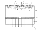
- FIG. 11 is a cross sectional view showing a cross sectional structure of a conventional semiconductor device.
- the p base region 102, the n + emitter region 103, and the gate on the front surface of the semiconductor substrate to be the n ⁇ drift region 101 in the active region 100a A MOS (metal-oxide-semiconductor insulated gate) structure including the oxide film 104 and the gate electrode 105 is provided.
- Emitter electrode 106 is in contact with p base region 102 and n + emitter region 103.
- Emitter electrode 106 is electrically insulated from gate electrode 105 by interlayer insulating film 107.
- a field limiting ring (FLR: floating p-type region) is formed on the front surface of the semiconductor substrate in the withstand voltage structure region 100 b which relaxes the electric field on the front surface side of the n ⁇ drift region 101 and holds the withstand voltage.
- FLR field limiting ring
- a Field Limiting Ring 111 and a Field Plate (FP) 112 connected to the FLR 111 are provided.
- FP Field Plate
- a p + collector layer 108 is provided on the surface layer on the back surface side of the semiconductor substrate.
- Collector electrode 109 is in contact with p + collector layer 108.
- An n-type field stop layer 110 having an impurity concentration higher than that of the n ⁇ drift region 101 is provided between the n ⁇ drift region 101 and the p + collector layer 108.
- the n-type field stop layer 110 prevents the depletion layer extending from the pn junction from reaching the p + collector layer 108 when the pn junction between the n ⁇ drift region 101 and the p base region 102 is reverse biased.
- the breakdown voltage of the device can be determined by the impurity concentration and thickness of the n-type field stop layer 110.
- n - impurity concentration of the drift region 101 by appropriately setting the impurity concentration and thickness of the n-type field stop layer 110, n - it is possible to reduce the thickness of the drift region 101, a low on-voltage The trade-off between cost reduction and loss reduction is improved.
- the n-type field stop layer 110 In the conventional process for forming the n-type field stop layer 110, first, the completed FS-IGBT of the semiconductor wafer is thinned to a desired thickness. Next, an n-type dopant such as phosphorus or selenium is implanted into the back surface of the semiconductor wafer, and the n-type dopant implanted into the back surface of the semiconductor wafer is activated by high temperature annealing at, for example, 600 ° C. or higher. Thus, the n-type field stop layer 110 is formed on the surface layer on the back surface of the semiconductor wafer. Thereafter, on the surface layer of the n-type field stop layer 110, the p + collector layer 108 shallower than the n-type field stop layer 110 is formed.
- an n-type dopant such as phosphorus or selenium is implanted into the back surface of the semiconductor wafer, and the n-type dopant implanted into the back surface of the semiconductor wafer is activated by
- the n-type field stop layer 110 when forming the n-type field stop layer 110 in this way, high-temperature annealing is performed to form the n-type field stop layer 110, so problems occur in the high-temperature annealing to form the front surface electrode and passivation protective film.
- the process should be performed after the formation of the n-type field stop layer 110. For this reason, the front surface electrode and the passivation protective film are formed on the thin semiconductor wafer after thinning, and the number of processes performed on the thin semiconductor wafer is increased. Therefore, the process load on the semiconductor wafer is large, which causes a reduction in yield.
- protons (H + ) are irradiated from the back surface of the semiconductor wafer and annealing treatment is performed, whereby the irradiated and implanted hydrogen atoms form complex defects together with the surrounding holes and the like.
- a method of forming an n-type field stop layer by using a hydrogen related donor in which the composite defect becomes a donor Protons can be easily extended in range as compared to phosphorus (P), selenium (Se) or the like, so proton irradiation can be performed to a desired depth even for a thick semiconductor wafer before thinning.
- the annealing temperature required for donor conversion is, for example, about 300 ° C.
- a donor layer by proton can be formed as an n-type field stop layer, and the process load on the semiconductor wafer can be reduced.
- the following method has been proposed as a method of manufacturing a semiconductor device in which the n-type field stop layer is formed by proton irradiation and low temperature annealing as described above.
- An element active area and an emitter electrode are formed on the front side of a low-cost FZ wafer, the back side of the wafer is scraped off to a predetermined thickness, and proton irradiation is then performed from the back side to perform low temperature annealing.
- a buffer layer + performs particle beam irradiation of boron ions from the back
- forming a p + collector layer is subjected to annealing treatment for irradiating light or laser to the wafer backside while cooling the wafer surface
- annealing treatment for irradiating light or laser to the wafer backside while cooling the wafer surface
- n-type defect layer substantially functions as an n + buffer layer (for example, see Patent Document 1 below).
- an IGBT manufacturing method for manufacturing a punch-through type IGBT in an N-type conductive float zone silicon wafer, comprising a plurality of base regions, source regions, gate grids and emitter electrodes.
- Forming a top structure comprising the top surface of the wafer, removing the float zone silicon from the bottom surface of the wafer to reduce the thickness of the wafer to a predetermined value, and Implanting hydrogen to a predetermined depth and concentration into the bottom to form an N + buffer layer, forming a P ⁇ -type collector region at the bottom of the N + buffer layer, and the P ⁇ -type Forming a back contact on the collector region and raising the temperature after the hydrogen implantation to a temperature that does not damage the top structure of the wafer.
- a step of performing annealing is proposed, and a method is proposed in which the hydrogen is injected in a plurality of successive separate steps of gradually decreasing the injection amount and gradually increasing the energy (see, for example, Patent Document 2 below). .
- N - type first becomes semiconductor layer N - After the introduction of oxygen into the mold FZ wafer, to form a P-type second semiconductor layer and an anode electrode on the surface of the FZ wafer.
- the FZ wafer is irradiated with protons from the side of the anode electrode to introduce crystal defects in the FZ wafer.
- the net doping concentration of a part of the first semiconductor layer is made higher than the original net doping concentration of the FZ wafer, and a desired broad buffer structure is formed.
- JP 2001-160559 A Japanese Patent Publication No. 2003-533047 Japanese Patent Publication No. 2007-055352
- Patent Document 1 since the acceleration energy of proton irradiation is 1 MeV or less, the half width of the field stop layer is as narrow as 10 ⁇ m or less, it is difficult to suppress the expansion of the depletion layer smoothly during switching, causing oscillation (noise) There is a risk that In Patent Document 2 described above, the proton irradiation is performed in plural times with acceleration energy of 500 keV or less to form a plurality of field stop layers, but the half width of each field stop layer is narrow. It is difficult to control growth smoothly.
- An object of the present invention is to provide a semiconductor device and a method of manufacturing the semiconductor device capable of reducing a leakage current in order to solve the above-mentioned problems of the prior art.
- Another object of the present invention is to provide a semiconductor device having a high withstand voltage and a method of manufacturing the semiconductor device, in order to solve the above-mentioned problems of the prior art.
- a method of manufacturing a semiconductor device has the following features.
- An irradiation step is performed on the back surface of the semiconductor substrate of the first conductivity type to perform two or more proton irradiations with the same range and different acceleration energy.
- annealing is performed to activate the protons irradiated in the irradiation step by annealing to form two or more first conductivity type semiconductor layers having a higher impurity concentration than the semiconductor substrate on the surface layer on the back surface of the semiconductor substrate. I do.
- a contact formation step of forming a contact layer to be a contact portion with the output electrode is performed on the surface layer on the back surface of the semiconductor substrate.
- an output electrode formation step of forming the output electrode in contact with the contact layer is performed.
- the proton irradiation is performed twice or more such that the surface layer on the back surface of the semiconductor substrate is positioned in the two or more first conductivity type semiconductor layers in the depth direction of the semiconductor substrate. Adjust the range of
- the absorbers having different thicknesses are used, and the combination of the different acceleration energy and the thickness of the absorbers is performed twice or more times.
- the irradiation step is characterized in that the proton irradiation is performed twice or more with different acceleration energy within the range of 1 MeV to 20 MeV.
- the annealing step is performed at least after the last proton irradiation.
- the annealing step is performed at a temperature within a range of 300 ° C. to 500 ° C.
- the annealing step is characterized in that annealing is performed within a range of 1 hour to 10 hours.
- a front surface element structure is further provided in which a front surface element structure is formed on the front surface of the semiconductor substrate before the irradiation step. Perform the formation process. Then, in the front surface element structure formation step, an insulation gate structure of an insulation gate bipolar transistor in which a channel of the first conductivity type is formed on the front surface of the semiconductor substrate is formed. In the contact forming step, a collector layer of a second conductivity type is formed as the contact layer.
- a front surface element structure is further formed to form a front surface element structure on the front surface of the semiconductor substrate before the irradiation step. Perform the formation process. Then, in the front surface element structure forming step, an anode region of the second conductivity type is formed on the surface layer of the front surface of the semiconductor substrate. In the contact forming step, a cathode layer of a first conductivity type is formed as the contact layer.
- the semiconductor device has the following features.
- a first semiconductor layer is provided on the surface layer on the back surface side of the semiconductor substrate of the first conductivity type.
- a second semiconductor layer of a first conductivity type in contact with the first semiconductor layer is provided inside the semiconductor substrate.
- the second semiconductor layer has a higher impurity concentration than the semiconductor substrate.
- An output electrode in contact with the first semiconductor layer is provided.
- the second semiconductor layer has an impurity concentration distribution in which the peak concentration is higher than the impurity concentration of the semiconductor substrate and decreases at a steep slope in the direction away from the first semiconductor layer.
- an impurity concentration in which the peak concentration is lower than that of the first first conductivity type semiconductor layer and decreases with a gentle slope in the direction away from the first semiconductor layer than that of the first first conductivity type semiconductor layer is comprised by the composite with the 2nd 1st conductivity type semiconductor layer which has distribution.
- either or both of the first first conductivity type semiconductor layer and the second first conductivity type semiconductor layer contain a hydrogen related donor. It features.
- the surface layer on the back surface side of the semiconductor substrate has the semiconductor in which the doping concentration of the second first conductivity type semiconductor layer is the semiconductor in the depth direction of the semiconductor substrate. It is characterized in that it is in a region above the doping concentration of the substrate.
- the surface layer on the back surface side of the semiconductor substrate may have a doping concentration of the second first conductivity type semiconductor layer in the depth direction of the semiconductor substrate. It is characterized in that it is in a region of 0.1 times or more of the maximum concentration of the first conductivity type semiconductor layer 2.
- the surface layer on the back surface side of the semiconductor substrate may have a doping concentration of the second first conductivity type semiconductor layer in the depth direction of the semiconductor substrate. It is characterized in that it is in a region of 0.5 times or more of the maximum concentration of the first conductivity type semiconductor layer 2.
- the surface layer on the back surface side of the semiconductor substrate has the semiconductor in which the doping concentration of the first first conductivity type semiconductor layer is the semiconductor in the depth direction of the semiconductor substrate. It is characterized in that it is in a region above the doping concentration of the substrate.
- the surface layer on the back surface side of the semiconductor substrate may have a doping concentration of the first first conductivity type semiconductor layer in the depth direction of the semiconductor substrate. It is characterized in that it is in a region of 0.1 times or more of the maximum concentration of the first conductivity type semiconductor layer of 1.
- the surface layer on the back surface side of the semiconductor substrate may have a doping concentration of the first first conductivity type semiconductor layer in the depth direction of the semiconductor substrate. It is characterized in that it is in a region of 0.5 times or more of the maximum concentration of the first conductivity type semiconductor layer of 1.
- the peak position of the first first conductivity type semiconductor layer is the peak position of the second first conductivity type semiconductor layer and the depth of the semiconductor substrate. It is characterized by being equal in direction.
- the peak position of the impurity concentration distribution of the first first conductive semiconductor layer and the second first conductive semiconductor layer may be the first semiconductor layer.
- the output electrode in the above-described invention, the peak position of the impurity concentration distribution of the first first conductive semiconductor layer and the second first conductive semiconductor layer may be the first semiconductor layer.
- the peak position of the impurity concentration distribution may be between the first first conductivity type semiconductor layer and the second first conductivity type semiconductor layer.
- the impurity concentration at the peak position is equal to that of the first conductive semiconductor layer of the first semiconductor layer and the semiconductor substrate and is lower than that of the first conductive semiconductor layer of the first semiconductor layer; It is characterized in that at least one or more first conductivity type semiconductor layers higher than the first conductivity type are provided.
- the semiconductor device further has the following features in the above-described invention.
- a second conductivity type semiconductor region is selectively provided in the surface layer on the front surface side of the semiconductor substrate.
- a first conductivity type semiconductor region is selectively provided in the second conductivity type semiconductor region.
- An input electrode is provided in contact with the second conductivity type semiconductor region and the first conductivity type semiconductor region.
- a control electrode is provided on the surface of a portion of the second conductivity type semiconductor region sandwiched by the semiconductor substrate and the first conductivity type semiconductor region, with an insulating film interposed therebetween. The first semiconductor layer of the second conductivity type is provided.
- the semiconductor device further has the following features in the above-described invention.
- a second conductivity type semiconductor region is selectively provided in the surface layer on the front surface side of the semiconductor substrate.
- An input electrode is provided in contact with the second conductivity type semiconductor region.
- the first semiconductor layer of the first conductivity type is provided.
- the peak position of the impurity concentration is equal to the depth direction of the semiconductor substrate and the impurity concentration at the peak position is equal by performing two or more times of proton irradiation with the same range and different acceleration energy. It is possible to form two or more first conductivity type semiconductor layers having an impurity concentration distribution which decreases with a gentle slope in a direction away from the first semiconductor layer as it is lower. For this reason, forming a first conductivity type semiconductor layer with few defects in the deep portion on the second conductivity type semiconductor region side from the back surface of the semiconductor substrate by proton irradiation with low acceleration energy among two or more proton irradiations. Can. Thereby, it is possible to suppress a decrease in lifetime while providing a donor layer having a defect caused by proton irradiation as a donor. Therefore, it is possible to suppress the speeding up of switching due to the extreme decrease of the lifetime at turn-off.
- the first conductivity type semiconductor layer with few defects is formed in a deep portion on the second conductivity type semiconductor region side from the back surface of the semiconductor substrate, thereby reducing leakage current at the time of reverse bias. be able to. Further, it is possible to form a first conductivity type semiconductor layer having an impurity concentration distribution which decreases at a gentle slope in a deep portion from the back surface of the semiconductor substrate to the second conductivity type semiconductor region side. Thereby, the oscillation at the time of switching can be suppressed.
- the semiconductor device and the method of manufacturing the semiconductor device according to the present invention it is possible to reduce the leakage current. Further, according to the semiconductor device and the method of manufacturing the semiconductor device according to the present invention, an effect that the withstand voltage can be improved is exhibited.
- FIG. 1 is a cross-sectional view showing the cross-sectional structure of the semiconductor device according to the first embodiment.
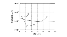
- FIG. 2 is a characteristic diagram showing the impurity concentration distribution of the field stop layer of the semiconductor device of FIG.
- FIG. 3 is a cross-sectional view showing the cross-sectional structure of the semiconductor device in the process of manufacturing according to the first embodiment.
- FIG. 4 is a cross-sectional view showing the cross-sectional structure of the semiconductor device in the process of manufacturing according to the first embodiment.
- FIG. 5 is a cross-sectional view showing the cross-sectional structure of the semiconductor device in the process of manufacturing according to the first embodiment.
- FIG. 6 is a cross-sectional view showing the cross-sectional structure of the semiconductor device in the process of manufacturing according to the first embodiment.
- FIG. 7-1 is a characteristic diagram showing the impurity concentration distribution along the section line A1-A2 in FIG.
- FIG. 7-2 is a characteristic diagram showing the impurity concentration distribution of the semiconductor device according to the first embodiment.
- FIG. 8 is a cross-sectional view showing a cross-sectional structure of the semiconductor device according to the second embodiment.
- FIG. 9 is a characteristic diagram showing the electrical characteristics of the semiconductor device according to the first embodiment.
- FIG. 10 is a characteristic diagram showing the electrical characteristics of the semiconductor device according to the second embodiment.
- FIG. 11 is a cross sectional view showing a cross sectional structure of a conventional semiconductor device.
- n and p in the layer or region having n or p, it is meant that electrons or holes are majority carriers, respectively.
- + and-attached to n and p mean that the impurity concentration is higher and the impurity concentration is lower than that of the layer or region to which it is not attached, respectively.
- the same components are denoted by the same reference numerals and redundant description will be omitted.
- the impurity concentration means, unless otherwise specified, the net doping concentration (net doping concentration) by donors and acceptors electrically activated inside the semiconductor.
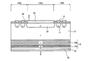
- FIG. 1 is a cross-sectional view showing the cross-sectional structure of the semiconductor device according to the first embodiment.
- FIG. 2 is a characteristic diagram showing the impurity concentration distribution of the field stop layer of the semiconductor device of FIG.
- the depth of 0 ⁇ m indicates the boundary between the p + collector layer 8 and the n-type field stop layer 10.
- the active region 100a through which current flows when the semiconductor device is turned on and the active region 100a are relaxed to alleviate the electric field on the front surface side of the n - drift region 1 and withstand voltage.
- the p base region 2 is provided in the surface layer on the front surface side of the semiconductor substrate to be the n ⁇ drift region 1.
- An n + emitter region 3 is selectively provided in the p base region 2 so as to be exposed to the front surface of the semiconductor substrate.
- a gate electrode 5 is provided on the surface of a portion of the p base region 2 sandwiched by the n ⁇ drift region 1 and the n + emitter region 3 via a gate oxide film 4.
- Emitter electrode 6 is provided on the front surface of the semiconductor substrate and is in contact with n + emitter region 3 and p base region 2. Emitter electrode 6 is electrically insulated from gate electrode 5 by interlayer insulating film 7.
- Field plate (FP) 12 is provided on the front surface of the semiconductor substrate and in contact with FLR 11.
- the p + collector layer 8 is provided from the active region 100 a to the breakdown voltage structure region 100 b.
- Collector electrode 9 is provided on the back surface of the semiconductor substrate and is in contact with p + collector layer 8.
- an n-type field stop layer 10 is provided in the n ⁇ drift region 1 so as to be in contact with the p + collector layer 8.
- the impurity concentration of the n-type field stop layer 10 is higher than the impurity concentration of the n ⁇ drift region 1.
- the n-type field stop layer 10 is formed of a composite of 10a and 10b as first and second n-type field stop layers.
- the first and second n-type field stop layers 10a and 10b both have an impurity concentration distribution such that the boundary between the p + collector layer 8 and the collector electrode 9, that is, the back surface of the semiconductor substrate after completion of the semiconductor device becomes a peak position. Is preferred.
- these n-type field stop layers 10 are irradiated with protons (H + ) from the back surface of the semiconductor wafer to perform annealing, so that the irradiated and implanted hydrogen atoms are composited with vacancies and the like in the periphery. It is a layer formed by using a hydrogen related donor in which a defect is formed and the composite defect becomes a donor.
- the first n-type field stop layer 10a has an impurity concentration distribution which decreases steeply toward the n + emitter region 3 side with respect to the second n-type field stop layer 10b, and the impurity concentration at its peak position is the second n-type It is higher than the impurity concentration distribution of the field stop layer 10b.
- the second n-type field stop layer 10b has an impurity concentration distribution which gradually decreases toward the n + -emitter region 3 side with respect to the first n-type field stop layer 10a. It is lower than the impurity concentration distribution of the 1 n-type field stop layer 10a.
- the impurity concentration at the peak position of the impurity concentration distribution is about halfway between the first n-type field stop layer 10 a and the second n-type field stop layer 10 b between the first n-type field stop layer 10 a and the second n-type field stop layer 10 b.
- a plurality of n-type field stop layers may be provided.
- the first n-type field stop layer 10 a has a higher impurity concentration than the second n-type field stop layer 10 b, and from the boundary with the p + collector layer 8, the n ⁇ drift region 1 It is provided shallower than the second n-type field stop layer 10 b inside.
- the depth from the boundary between the first n-type field stop layer 10a and the p + collector layer 8 may be, for example, 5 ⁇ m to 10 ⁇ m.
- the second n-type field stop layer 10 b is provided deeper than the first n-type field stop layer 10 a in the n ⁇ drift region 1 from the boundary with the p + collector layer 8.
- the depth from the boundary between the second n-type field stop layer 10 b and the p + collector layer 8 may be, for example, 30 ⁇ m.
- the n-type field stop layer 10 has the first and second n-type field stop layers 10a, 10b having different impurity concentrations at the peak position and having an impurity concentration distribution decreasing at different inclinations toward the n + emitter region 3 side. It consists of 10b.
- the impurity concentration is higher at a predetermined depth from the boundary with p + collector layer 8 and deeper than p + collector layer 8 inside the semiconductor substrate than in Conventional Example 1 shown by dotted lines in FIG.
- An n-type field stop layer 10 having a low impurity concentration is formed in the region.
- the conventional example 1 is a semiconductor device in which one n-type field stop layer 41 is formed so that the withstand voltage becomes equal to that of the semiconductor device according to the first embodiment by one proton irradiation.
- FIG. 7-1 is a characteristic diagram showing the impurity concentration distribution along the section line A1-A2 in FIG.
- a MOS structure consisting of p base region 2, n + emitter region 3, gate oxide film 4 and gate electrode 5 is formed.
- emitter electrode 6 in contact with p base region 2 and n + emitter region 3 is formed.
- an absorber 20 for adjusting the range of protons is disposed at a predetermined distance on the back surface side of the semiconductor substrate.
- the absorber is, for example, a plate-like member made of aluminum or the like.
- the first proton irradiation 21 for forming the first n-type field stop layer 10 a is performed on the entire back surface of the semiconductor substrate at the range Rp adjusted via the absorber 20.
- the range Rp of the first proton irradiation 21 is adjusted by the thickness of the absorber 20 to a position to be the back surface of the semiconductor substrate after thinning.
- the first proton irradiation 21 may have, for example, an acceleration energy of 2 MeV and an irradiation amount of 1 ⁇ 10 13 / cm 2 . It is well known that the acceleration energy is adjusted by an acceleration voltage of a cyclotron or a linear accelerator which performs proton irradiation.
- a second n-type field stop layer 10b is formed on the entire back surface of the semiconductor substrate through an absorber 20a having a thickness different from that used in the first proton irradiation 21.
- 2 Proton irradiation 22 is performed.
- the range of the second proton irradiation 22 is adjusted to the same range Rp as the first proton irradiation 21 using the absorber 20 a.
- the acceleration energy of the second proton irradiation 22 is higher than the acceleration energy of the first proton irradiation 21.
- the absorber 20 of the first proton irradiation 21 when used, the proton of the second proton irradiation 22 penetrates into the semiconductor substrate deeper than the range Rp of the first proton irradiation 21. Therefore, in order to make the range of the second proton irradiation 22 the same as the range Rp of the first proton irradiation 21, the thickness of the absorber 20 a used for the second proton irradiation 22 is the same as the absorber used for the first proton irradiation 21. Must be thicker than 20.
- the second proton irradiation 22 may have, for example, an acceleration energy of 8 MeV and an irradiation amount of 1 ⁇ 10 13 / cm 2 .
- Each proton irradiation may be performed, for example, at different acceleration energies in the range of 1 MeV to 20 MeV, preferably 2 MeV to 8 MeV.
- annealing is performed, and the crystal defects formed by the first and second proton irradiations 21 and 22 are donated (activated).
- the annealing may be performed once for each proton irradiation, or may be performed at least only after the last proton irradiation.
- Annealing may be performed, for example, at a temperature within the range of 300 ° C. to 500 ° C., and within the range of 1 hour to 10 hours.
- first and second n-type field stop layers 10a and 10b having a position to be the back surface of the semiconductor substrate after thinning down as a peak position of the impurity concentration respectively have a predetermined half width. It is formed.
- the impurity concentration distribution of the first and second n-type field stop layers 10a and 10b after donor conversion will be described later.
- the back surface of the semiconductor substrate is ground, and among the n-type layers formed by the first and second proton irradiations 21 and 22, the n + emitter region 3 side from the peak position of the impurity concentration Only the n-type layer 23 up to the boundary with the n ⁇ drift region 1 is left as the n-type field stop layer 10.
- the thicknesses of the absorber 20 and the absorber 20a are appropriately adjusted.
- the first and second n-type field stop layers 10a and 10b having different peak positions of the impurity concentration distribution are formed, the first n-type field stop layer 10a or the second n-type field stop layer 10b and the back side surface layer of the semiconductor substrate The back surface grinding of the semiconductor substrate after donor conversion is performed so that (p + collector layer 8) satisfies the positional relationship to be described later.
- the first n-type field stop layer 10a formed by the first proton irradiation 21 and the second n-type formed by the second proton irradiation 22 are formed inside the semiconductor substrate after donor conversion.
- Field stop layer 10b is formed to overlap with the peak position of the impurity concentration distribution in the same manner.
- the impurity concentration distribution of the first n-type field stop layer 10a has a high peak position, and a sharp half width of the decreasing degree of the impurity concentration from the peak position is narrow.
- the impurity concentration distribution of the second n-type field stop layer 10 b has a low peak position and a broad half-value width of a gradual decrease in the impurity concentration from the peak position.
- n-type layer 23 as the n-type field stop layer 10 from the peak position of the impurity concentration to the n + emitter region 3 side end, the n-type field stop having the desired impurity concentration distribution shown in FIG. Layer 10 can be obtained.
- FIG. 7-2 is a characteristic diagram showing the impurity concentration distribution of the semiconductor device according to the first embodiment.
- FIG. 7-2 shows the positional relationship between the first n-type field stop layer 10a or the second n-type field stop layer 10b of the present invention and the back surface side surface layer of the semiconductor substrate.
- the impurity concentration in the vertical direction (the position indicated by N0 is the substrate concentration), and the depth from the back surface D0 of the semiconductor substrate after completion of the device in the horizontal direction.
- the semiconductor substrate back surface D0 after completion of the device is the back surface position after completion of the semiconductor device in which the back surface of the semiconductor substrate is ground and thinned during the process.
- the portion on the left side of the back surface D0 of the semiconductor substrate after completion of the device is a portion to be removed by grinding the semiconductor substrate during the process.
- a p + collector layer (not shown) is formed on the surface layer of the back surface D0 of the semiconductor substrate after completion of the device (hereinafter referred to as the surface layer on the back surface side of the semiconductor substrate).
- the surface layer (p + collector layer) on the back side of the semiconductor substrate is in the region of the first n-type field stop layer 10a or the second n-type field stop layer 10b, that is, in the region of higher concentration than the concentration of the semiconductor substrate. If so, the effects of the present invention can be achieved.
- the surface layer on the back surface side of the semiconductor substrate may be in a region of 0.1 times or more of each field stop layer peak concentration (maximum concentration) Np. More preferably, as indicated by symbol B2, the surface layer on the back surface side of the semiconductor substrate may be in a region of 0.5 times or more the peak concentration (maximum concentration) Np of each field stop layer.
- the code B1 shows the case where the semiconductor substrate back surface D0 after completion of the device is at each field stop layer peak concentration Np. Further, as a comparative example, a case where the surface layer on the back surface side of the semiconductor substrate after completion of the device is in a region of a concentration lower than the concentration of the semiconductor substrate is indicated by a rough dotted line. In the case where the substrate concentration N0 is higher than 0.1 Np or 0.5 Np, the surface layer on the back surface side of the semiconductor substrate may be in a region having a concentration higher than the substrate concentration of the semiconductor substrate.
- the first proton irradiation 21 may be performed after the second proton irradiation 22 in the reverse order of the first and second proton irradiations 21 and 22 described above.
- the first and second proton irradiations 21 and 22 may be performed from the front surface side of the semiconductor substrate.
- adjustment of the range Rp of the first and second proton irradiations 21 and 22 becomes easy.
- the acceleration energy of the first and second proton irradiations 21 and 22 may be higher than that of the first proton irradiation 21 as described above, for example, in the range of 1 MeV to 10 MeV.
- the irradiation dose of the first and second proton irradiations 21 and 22 can be variously changed in the range of 1 ⁇ 10 12 / cm 2 to 1 ⁇ 10 15 / cm 2 .
- the peak position of the impurity concentration is in the depth direction of the semiconductor substrate. It is possible to form first and second n-type field stop layers that are equal and have different impurity concentrations and impurity concentration distributions at peak positions. Therefore, the second proton irradiation is performed at an acceleration energy lower than that of the first proton to form the second n-type field stop layer with few defects in the deep portion on the n + emitter region side from the back surface of the semiconductor substrate. Can. Thereby, it is possible to suppress a decrease in lifetime while providing a donor region in which a defect due to proton irradiation is a donor. Therefore, it is possible to suppress the speeding up of switching due to the extreme decrease of the lifetime at turn-off.
- the second n-type field stop layer with few defects in the deep portion on the n + emitter region side from the back surface of the semiconductor substrate, the leakage current at the time of reverse bias can be reduced.
- the second n-type field stop layer having an impurity concentration distribution which gradually decreases toward the n + emitter region side can be formed in a deep portion on the n + emitter region side from the back surface of the semiconductor substrate. Thereby, oscillation at the time of switching can also be suppressed.
- a portion of the n-type field stop layer in contact with the collector layer is more than the second n-type field stop layer.
- a first n-type field stop layer having a high impurity concentration can be formed.
- the impurity concentration distribution decreases with a gentle slope toward the n + emitter region side, whereby the pn junction between the p base region and the n ⁇ drift region Elongation of the extending depletion layer can be smoothly suppressed.
- the impurity concentration is higher than that of the second n-type field stop layer, so that the depletion layer can be prevented from reaching the p + collector layer.
- FIG. 8 is a cross-sectional view showing a cross-sectional structure of the semiconductor device according to the second embodiment.
- the semiconductor device according to the second embodiment differs from the semiconductor device according to the first embodiment in that a diode is used instead of the IGBT.
- ap + anode region 32 is selectively provided in the surface layer on the front surface side of the n ⁇ -type semiconductor substrate 31.
- the anode electrode 33 is in contact with the p + anode region 32.
- Reference numeral 34 denotes an interlayer insulating film.
- an n + cathode layer 35 is provided on the surface layer on the back surface side of the n ⁇ -type semiconductor substrate 31, and an n type field stop layer 10 is provided in a region deeper than the n + cathode layer 35 on the back surface side. There is.
- the n-type field stop layer 10 is formed of the first and second n-type field stop layers 10 a and 10 b.
- the cathode electrode 36 contacts the n + cathode layer 35.
- the manufacturing method of the semiconductor device concerning Embodiment 2 is the same as the manufacturing method of the semiconductor device concerning Embodiment 1 except formation of element structure of a diode formed of a general method.
- the same effect as that of the first embodiment can be obtained. Further, according to the second embodiment, even in the case of the diode, by providing the first and second n-type field stop layers 10a and 10b, the decrease in carrier concentration in the vicinity of the cathode layer can be suppressed. For this reason, it is possible to suppress hardware recovery, which is a main cause of diode noise, and to achieve high breakdown voltage.
- FIG. 9 is a characteristic diagram showing the electrical characteristics of the semiconductor device according to the first embodiment.
- FIG. 9 shows a leak current waveform at the time of reverse bias.
- an IGBT provided with the first and second n-type field stop layers 10a and 10b was manufactured (hereinafter, referred to as example 1).
- Conventional Example 1 indicated by a dotted line in FIG. 7-1 was produced, in which one n-type field stop layer was formed so that the withstand voltage was equalized with that of Example 1 by one proton irradiation.
- the leak current at the time of reverse bias was measured.
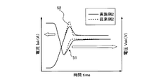
- FIG. 10 is a characteristic diagram showing the electrical characteristics of the semiconductor device according to the second embodiment.
- FIG. 10 shows a reverse recovery waveform of (FWD: Free Wheeling Diode).
- FWD Free Wheeling Diode
- an FWD provided with the first and second n-type field stop layers 10a and 10b was manufactured (hereinafter referred to as example 2).
- Conventional Example 2 in which one n-type field stop layer was formed so that the withstand voltage was equal to that of Example 2 by one proton irradiation was manufactured. Then, in each of Example 2 and Conventional Example 2, the surge voltage and reverse current at the time of reverse recovery were measured.
- the present invention is not limited to the above-described embodiments, and various modifications can be made.
- three or more proton irradiations with different acceleration energy may be performed to form three or more n-type field stop layers having the same peak position of impurity concentration and different impurity concentration at the peak position.
- the present invention can be applied to various semiconductor devices in which a field stop layer can be provided.
- the planar gate IGBT is described as an example, but may be applied to a trench gate IGBT.
- the semiconductor device and the method for manufacturing the semiconductor device according to the present invention are useful for a semiconductor device used for a power conversion device such as a converter or an inverter.
- n type field stop layer 10 a first n type field stop layer 10 b Second n-type field stop layer 20, 20a absorber 22 second proton irradiation 23 n-type semiconductor layer from the peak position of the impurity concentration to the end of n + emitter region 3
Abstract
Description
特徴とする。 Further, in the semiconductor device according to the present invention, in the above-described invention, the surface layer on the back surface side of the semiconductor substrate may have a doping concentration of the second first conductivity type semiconductor layer in the depth direction of the semiconductor substrate. It is characterized in that it is in a region of 0.1 times or more of the maximum concentration of the first conductivity
実施の形態1にかかる半導体装置の断面構造について、例えばプレーナゲート型IGBTを例に説明する。図1は、実施の形態1にかかる半導体装置の断面構造を示す断面図である。図2は、図1の半導体装置のフィールドストップ層の不純物濃度分布を示す特性図である。図2において、深さ0μmはp+コレクタ層8とn型フィールドストップ層10との境界を示す。図1に示す実施の形態1にかかる半導体装置には、半導体装置のオン時に電流が流れる活性領域100aと、活性領域100aを囲みn-ドリフト領域1のおもて面側の電界を緩和し耐圧を保持する耐圧構造領域100bと、を備える。 Embodiment 1
The cross-sectional structure of the semiconductor device according to the first embodiment will be described using, for example, a planar gate IGBT as an example. FIG. 1 is a cross-sectional view showing the cross-sectional structure of the semiconductor device according to the first embodiment. FIG. 2 is a characteristic diagram showing the impurity concentration distribution of the field stop layer of the semiconductor device of FIG. In FIG. 2, the depth of 0 μm indicates the boundary between the p + collector layer 8 and the n-type
図8は、実施の形態2にかかる半導体装置の断面構造を示す断面図である。実施の形態2にかかる半導体装置が実施の形態1にかかる半導体装置と異なる点は、IGBTに代えてダイオードを構成した点である。 Second Embodiment
FIG. 8 is a cross-sectional view showing a cross-sectional structure of the semiconductor device according to the second embodiment. The semiconductor device according to the second embodiment differs from the semiconductor device according to the first embodiment in that a diode is used instead of the IGBT.
図9は、実施例1にかかる半導体装置の電気特性を示す特性図である。図9には、逆バイアス時のリーク電流波形を示す。実施の形態1にかかる半導体装置の製造方法に従い、第1,2n型フィールドストップ層10a,10bを設けたIGBTを作製した(以下、実施例1とする)。比較として、1回のプロトン照射によって実施例1と耐圧が等しくなるように1つのn型フィールドストップ層を形成した図7-1に点線で示す従来例1を作製した。そして、実施例1および従来例1のそれぞれにおいて、逆バイアス時のリーク電流を測定した。 Example 1
FIG. 9 is a characteristic diagram showing the electrical characteristics of the semiconductor device according to the first embodiment. FIG. 9 shows a leak current waveform at the time of reverse bias. In accordance with the method of manufacturing a semiconductor device according to the first embodiment, an IGBT provided with the first and second n-type field stop layers 10a and 10b was manufactured (hereinafter, referred to as example 1). As a comparison, Conventional Example 1 indicated by a dotted line in FIG. 7-1 was produced, in which one n-type field stop layer was formed so that the withstand voltage was equalized with that of Example 1 by one proton irradiation. Then, in each of Example 1 and Conventional Example 1, the leak current at the time of reverse bias was measured.
図10は、実施例2にかかる半導体装置の電気特性を示す特性図である。図10には、(FWD:Free Wheeling Diode)の逆回復波形を示す。実施の形態2にかかる半導体装置の製造方法に従い、第1,2n型フィールドストップ層10a,10bを設けたFWDを作製した(以下、実施例2とする)。比較として、1回のプロトン照射によって実施例2と耐圧が等しくなるように1つのn型フィールドストップ層を形成した従来例2を作製した。そして、実施例2および従来例2のそれぞれにおいて、逆回復時のサージ電圧および逆方向電流を測定した。 (Example 2)
FIG. 10 is a characteristic diagram showing the electrical characteristics of the semiconductor device according to the second embodiment. FIG. 10 shows a reverse recovery waveform of (FWD: Free Wheeling Diode). In accordance with the method of manufacturing a semiconductor device according to the second embodiment, an FWD provided with the first and second n-type field stop layers 10a and 10b was manufactured (hereinafter referred to as example 2). As a comparison, Conventional Example 2 in which one n-type field stop layer was formed so that the withstand voltage was equal to that of Example 2 by one proton irradiation was manufactured. Then, in each of Example 2 and Conventional Example 2, the surge voltage and reverse current at the time of reverse recovery were measured.
2 pベース領域
3 n+エミッタ領域
4 ゲート酸化膜
5 ゲート電極
6 エミッタ電極
7 層間絶縁膜
8 p+コレクタ層
9 コレクタ電極
10 n型フィールドストップ層
10a 第1n型フィールドストップ層
10b 第2n型フィールドストップ層
20,20a アブソーバ
22 第2プロトン照射
23 不純物濃度のピーク位置からn+エミッタ領域3端部までのn型半導体層 1 n − drift region 2 p base region 3 n + emitter region 4
Claims (21)
- 第1導電型の半導体基板の裏面に、加速エネルギーが異なる2回以上のプロトン照射を行う照射工程と、
アニールによって前記照射工程で照射されたプロトンを活性化し、前記半導体基板の裏面の表面層に前記半導体基板よりも不純物濃度が高い2つ以上の第1導電型半導体層を形成するアニール工程と、
前記アニール工程後、前記半導体基板の裏面の表面層に、出力電極との接触部となるコンタクト層を形成するコンタクト形成工程と、
前記コンタクト層に接する前記出力電極を形成する出力電極形成工程と、
を含み、
前記照射工程では、前記半導体基板の深さ方向において、前記2つ以上の第1導電型半導体層内に前記半導体基板の裏面の表面層が位置するように、前記2回以上のプロトン照射の飛程をそれぞれ調整することを特徴とする半導体装置の製造方法。 An irradiation step of performing two or more times of proton irradiation with different acceleration energy on the back surface of the semiconductor substrate of the first conductivity type;
Annealing to activate the protons irradiated in the irradiation step by annealing to form two or more first conductivity type semiconductor layers having a higher impurity concentration than the semiconductor substrate on the surface layer on the back surface of the semiconductor substrate;
A contact forming step of forming a contact layer to be a contact portion with an output electrode on the surface layer on the back surface of the semiconductor substrate after the annealing step;
An output electrode forming step of forming the output electrode in contact with the contact layer;
Including
In the irradiation step, the two or more times of proton irradiation fly so that the surface layer of the back surface of the semiconductor substrate is positioned in the two or more first conductivity type semiconductor layers in the depth direction of the semiconductor substrate. A method of manufacturing a semiconductor device, comprising adjusting each of the ranges. - 前記照射工程では、厚さが異なるアブソーバを用いて、前記異なる加速エネルギーと前記アブソーバの厚さとの組合せにより、前記2回以上のプロトン照射の飛程をそれぞれ調整することを特徴とする請求項1に記載の半導体装置の製造方法。 In the irradiation step, ranges of the two or more proton irradiations are respectively adjusted using a combination of the different acceleration energy and the thickness of the absorber using absorbers having different thicknesses. The manufacturing method of the semiconductor device as described in these.
- 前記照射工程では、1MeV~20MeVの範囲内の異なる加速エネルギーで前記2回以上のプロトン照射を行うことを特徴とする請求項1に記載の半導体装置の製造方法。 2. The method of manufacturing a semiconductor device according to claim 1, wherein in the irradiation step, the proton irradiation is performed twice or more with different acceleration energy in a range of 1 MeV to 20 MeV.
- 前記アニール工程は、少なくとも最後のプロトン照射後に行われることを特徴とする請求項1に記載の半導体装置の製造方法。 The method of manufacturing a semiconductor device according to claim 1, wherein the annealing step is performed at least after the last proton irradiation.
- 前記アニール工程では、300℃~500℃の範囲内の温度でアニールを行うことを特徴とする請求項1に記載の半導体装置の製造方法。 The method of manufacturing a semiconductor device according to claim 1, wherein the annealing is performed at a temperature in a range of 300 ° C to 500 ° C.
- 前記アニール工程では、1時間~10時間の範囲内でアニールを行うことを特徴とする請求項1に記載の半導体装置の製造方法。 The method of manufacturing a semiconductor device according to claim 1, wherein the annealing process is performed within a range of 1 hour to 10 hours.
- 前記照射工程前に、前記半導体基板のおもて面におもて面素子構造を形成するおもて面素子構造形成工程をさらに備え、
前記おもて面素子構造形成工程では、前記半導体基板のおもて面に第1導電型のチャネルを形成する絶縁ゲート型バイポーラトランジスタの絶縁ゲート構造を形成し、
前記コンタクト形成工程では、前記コンタクト層として第2導電型のコレクタ層を形成することを特徴とする請求項1~6のいずれか一つに記載の半導体装置の製造方法。 Before the irradiation step, the method further comprises a front surface element structure forming step of forming a front surface element structure on the front surface of the semiconductor substrate,
In the front surface element structure forming step, an insulating gate structure of an insulated gate bipolar transistor in which a channel of a first conductivity type is formed on the front surface of the semiconductor substrate is formed.
7. The method of manufacturing a semiconductor device according to claim 1, wherein a collector layer of a second conductivity type is formed as the contact layer in the contact formation step. - 前記照射工程前に、前記半導体基板のおもて面におもて面素子構造を形成するおもて面素子構造形成工程をさらに備え、
前記おもて面素子構造形成工程では、前記半導体基板のおもて面の表面層に第2導電型のアノード領域を形成し、
前記コンタクト形成工程では、前記コンタクト層として第1導電型のカソード層を形成することを特徴とする請求項1~6のいずれか一つに記載の半導体装置の製造方法。 Before the irradiation step, the method further comprises a front surface element structure forming step of forming a front surface element structure on the front surface of the semiconductor substrate,
In the front surface element structure forming step, an anode region of a second conductivity type is formed on the surface layer of the front surface of the semiconductor substrate,
The method of manufacturing a semiconductor device according to any one of claims 1 to 6, wherein a cathode layer of a first conductivity type is formed as the contact layer in the contact formation step. - 第1導電型の半導体基板と、
前記半導体基板の裏面側の表面層に設けられた第1半導体層と、
前記半導体基板の内部に設けられ、前記第1半導体層に接する、前記半導体基板よりも不純物濃度が高い第1導電型の第2半導体層と、
前記第1半導体層に接する出力電極と、
を備え、
前記第2半導体層は、ピーク濃度が前記半導体基板の不純物濃度よりも高くかつ前記第1半導体層から離れる方向に急峻な傾斜で減少する不純物濃度分布を有する第1の第1導電型半導体層と、ピーク濃度が前記第1の第1導電型半導体層よりも低く、かつ前記第1の第1導電型半導体層よりも前記第1半導体層から離れる方向に緩やかな傾斜で減少する不純物濃度分布を有する第2の第1導電型半導体層との複合によって構成されていることを特徴とする半導体装置。 A semiconductor substrate of a first conductivity type;
A first semiconductor layer provided on a surface layer on the back side of the semiconductor substrate;
A second semiconductor layer of a first conductivity type provided inside the semiconductor substrate and in contact with the first semiconductor layer, wherein the second semiconductor layer has a higher impurity concentration than the semiconductor substrate;
An output electrode in contact with the first semiconductor layer;
Equipped with
The second semiconductor layer has a first first conductivity type semiconductor layer having an impurity concentration distribution in which the peak concentration is higher than the impurity concentration of the semiconductor substrate and decreases at a steep slope in a direction away from the first semiconductor layer; An impurity concentration distribution in which the peak concentration is lower than that of the first first conductivity type semiconductor layer and decreases with a gentle slope in the direction away from the first semiconductor layer than that of the first first conductivity type semiconductor layer; What is claimed is: 1. A semiconductor device comprising a composite with a second first conductivity type semiconductor layer. - 前記第1の第1導電型半導体層または前記第2の第1導電型半導体層のいずれかもしくは両方が、水素関連ドナーを含むことを特徴とする請求項9に記載の半導体装置。 10. The semiconductor device according to claim 9, wherein one or both of the first first conductivity type semiconductor layer and the second first conductivity type semiconductor layer include a hydrogen related donor.
- 前記半導体基板の裏面側の表面層は、前記半導体基板の深さ方向において前記第2の第1導電型半導体層のドーピング濃度が前記半導体基板のドーピング濃度以上の領域にあることを特徴とする請求項9に記載の半導体装置。 The surface layer on the back surface side of the semiconductor substrate is characterized in that the doping concentration of the second first conductivity type semiconductor layer is in a region higher than the doping concentration of the semiconductor substrate in the depth direction of the semiconductor substrate. 10. A semiconductor device according to item 9.
- 前記半導体基板の裏面側の表面層は、前記半導体基板の深さ方向において前記第2の第1導電型半導体層のドーピング濃度が該第2の第1導電型半導体層の最大濃度の0.1倍以上の領域にあることを特徴とする請求項9に記載の半導体装置。 In the surface layer on the back surface side of the semiconductor substrate, the doping concentration of the second first conductivity type semiconductor layer is 0.1 of the maximum concentration of the second first conductivity type semiconductor layer in the depth direction of the semiconductor substrate. 10. The semiconductor device according to claim 9, wherein the semiconductor device is at least twice as large.
- 前記半導体基板の裏面側の表面層は、前記半導体基板の深さ方向において前記第2の第1導電型半導体層のドーピング濃度が該第2の第1導電型半導体層の最大濃度の0.5倍以上の領域にあることを特徴とする請求項12に記載の半導体装置。 In the surface layer on the back surface side of the semiconductor substrate, the doping concentration of the second first conductivity type semiconductor layer in the depth direction of the semiconductor substrate is 0.5 of the maximum concentration of the second first conductivity type semiconductor layer The semiconductor device according to claim 12, wherein the semiconductor device is in a double or more area.
- 前記半導体基板の裏面側の表面層は、前記半導体基板の深さ方向において前記第1の第1導電型半導体層のドーピング濃度が前記半導体基板のドーピング濃度以上の領域にあることを特徴とする請求項9に記載の半導体装置。 The surface layer on the back surface side of the semiconductor substrate is characterized in that the doping concentration of the first first conductivity type semiconductor layer is in a region higher than the doping concentration of the semiconductor substrate in the depth direction of the semiconductor substrate. 10. A semiconductor device according to item 9.
- 前記半導体基板の裏面側の表面層は、前記半導体基板の深さ方向において前記第1の第1導電型半導体層のドーピング濃度が該第1の第1導電型半導体層の最大濃度の0.1倍以上の領域にあることを特徴とする請求項9に記載の半導体装置。 In the surface layer on the back surface side of the semiconductor substrate, the doping concentration of the first first conductivity type semiconductor layer in the depth direction of the semiconductor substrate is 0.1 of the maximum concentration of the first first conductivity type semiconductor layer. 10. The semiconductor device according to claim 9, wherein the semiconductor device is at least twice as large.
- 前記半導体基板の裏面側の表面層は、前記半導体基板の深さ方向において前記第1の第1導電型半導体層のドーピング濃度が該第1の第1導電型半導体層の最大濃度の0.5倍以上の領域にあることを特徴とする請求項15に記載の半導体装置。 In the surface layer on the back surface side of the semiconductor substrate, the doping concentration of the first first conductivity type semiconductor layer in the depth direction of the semiconductor substrate is 0.5 of the maximum concentration of the first first conductivity type semiconductor layer The semiconductor device according to claim 15, wherein the semiconductor device is at least twice as large.
- 前記第1の第1導電型半導体層のピーク位置は、前記第2の第1導電型半導体層のピーク位置と前記半導体基板の深さ方向において等しいことを特徴とする請求項9に記載の半導体装置。 10. The semiconductor according to claim 9, wherein the peak position of the first first conductivity type semiconductor layer is equal to the peak position of the second first conductivity type semiconductor layer in the depth direction of the semiconductor substrate. apparatus.
- 前記第1の第1導電型半導体層および前記第2の第1導電型半導体層は、不純物濃度分布のピーク位置が前記第1半導体層と前記出力電極との境界となるように設けられていることを特徴とする請求項9に記載の半導体装置。 The first first conductivity type semiconductor layer and the second first conductivity type semiconductor layer are provided such that the peak position of the impurity concentration distribution is at the boundary between the first semiconductor layer and the output electrode. The semiconductor device according to claim 9,
- 前記第1の第1導電型半導体層と前記第2の第1導電型半導体層との間に、不純物濃度分布のピーク位置が前記第1の第1導電型半導体層と前記半導体基板の深さ方向に等しく、かつピーク位置の不純物濃度が前記第1の第1導電型半導体層よりも低く、前記第2の第1導電型半導体層よりも高い第1導電型半導体層が少なくとも1つ以上設けられていることを特徴とする請求項9に記載の半導体装置。 The peak position of the impurity concentration distribution is the depth of the first first conductivity type semiconductor layer and the semiconductor substrate between the first first conductivity type semiconductor layer and the second first conductivity type semiconductor layer. Of at least one first conductivity type semiconductor layer equal to the direction and having an impurity concentration at a peak position lower than that of the first first conductivity type semiconductor layer and higher than that of the second first conductivity type semiconductor layer The semiconductor device according to claim 9, characterized in that:
- 前記半導体基板のおもて面側の表面層に選択的に設けられた第2導電型半導体領域と、
前記第2導電型半導体領域の内部に選択的に設けられた第1導電型半導体領域と、
前記第2導電型半導体領域および前記第1導電型半導体領域に接する入力電極と、
前記第2導電型半導体領域の、前記半導体基板と前記第1導電型半導体領域とに挟まれた部分の表面に絶縁膜を介して設けられた制御電極と、
第2導電型の前記第1半導体層と、
を備えることを特徴とする請求項9~19のいずれか一つに記載の半導体装置。 A second conductivity type semiconductor region selectively provided in a surface layer on the front surface side of the semiconductor substrate;
A first conductivity type semiconductor region selectively provided inside the second conductivity type semiconductor region;
An input electrode in contact with the second conductivity type semiconductor region and the first conductivity type semiconductor region;
A control electrode provided on a surface of a portion of the second conductivity type semiconductor region sandwiched by the semiconductor substrate and the first conductivity type semiconductor region via an insulating film;
The first semiconductor layer of the second conductivity type;
The semiconductor device according to any one of claims 9 to 19, comprising: - 前記半導体基板のおもて面側の表面層に選択的に設けられた第2導電型半導体領域と、
前記第2導電型半導体領域に接する入力電極と、
第1導電型の前記第1半導体層と、
を備えることを特徴とする請求項9~19のいずれか一つに記載の半導体装置。 A second conductivity type semiconductor region selectively provided in a surface layer on the front surface side of the semiconductor substrate;
An input electrode in contact with the second conductivity type semiconductor region;
The first semiconductor layer of the first conductivity type;
The semiconductor device according to any one of claims 9 to 19, comprising:
Priority Applications (3)
| Application Number | Priority Date | Filing Date | Title |
|---|---|---|---|
| US14/372,454 US11152224B2 (en) | 2012-03-23 | 2013-03-15 | Semiconductor device with field stop layer and semiconductor device manufacturing method thereof |
| EP13764095.9A EP2793267B1 (en) | 2012-03-23 | 2013-03-15 | Semiconductor device and semiconductor device manufacturing method |
| JP2014506210A JP5754545B2 (en) | 2012-03-23 | 2013-03-15 | Semiconductor device and manufacturing method of semiconductor device |
Applications Claiming Priority (2)
| Application Number | Priority Date | Filing Date | Title |
|---|---|---|---|
| JP2012-067535 | 2012-03-23 | ||
| JP2012067535 | 2012-03-23 |
Publications (1)
| Publication Number | Publication Date |
|---|---|
| WO2013141181A1 true WO2013141181A1 (en) | 2013-09-26 |
Family
ID=49222640
Family Applications (1)
| Application Number | Title | Priority Date | Filing Date |
|---|---|---|---|
| PCT/JP2013/057562 WO2013141181A1 (en) | 2012-03-23 | 2013-03-15 | Semiconductor device and semiconductor device manufacturing method |
Country Status (4)
| Country | Link |
|---|---|
| US (1) | US11152224B2 (en) |
| EP (1) | EP2793267B1 (en) |
| JP (1) | JP5754545B2 (en) |
| WO (1) | WO2013141181A1 (en) |
Cited By (11)
| Publication number | Priority date | Publication date | Assignee | Title |
|---|---|---|---|---|
| WO2015087507A1 (en) * | 2013-12-10 | 2015-06-18 | 株式会社アルバック | Insulated gate bipolar transistor and production method therefor |
| WO2015141257A1 (en) * | 2014-03-19 | 2015-09-24 | サンケン電気株式会社 | Semiconductor device |
| JP2015201476A (en) * | 2014-04-04 | 2015-11-12 | 三菱電機株式会社 | Semiconductor device and manufacturing method of the same |
| WO2016063683A1 (en) * | 2014-10-24 | 2016-04-28 | 富士電機株式会社 | Semiconductor device and method for producing semiconductor device |
| JP2017005180A (en) * | 2015-06-15 | 2017-01-05 | 三菱電機株式会社 | Semiconductor device manufacturing method and semiconductor device |
| JPWO2016120999A1 (en) * | 2015-01-27 | 2017-04-27 | 三菱電機株式会社 | Semiconductor device |
| JP2017098318A (en) * | 2015-11-19 | 2017-06-01 | 三菱電機株式会社 | Semiconductor device and manufacturing method of the same |
| KR101928395B1 (en) * | 2017-04-26 | 2018-12-13 | (주) 트리노테크놀로지 | Power semiconductor device and manufacturing method thereof |
| WO2019017034A1 (en) * | 2017-07-19 | 2019-01-24 | 三菱電機株式会社 | Method for manufacturing semiconductor device, and semiconductor device |
| JP2020107917A (en) * | 2016-12-27 | 2020-07-09 | 三菱電機株式会社 | Manufacturing method of semiconductor device |
| JP2022019921A (en) * | 2019-09-11 | 2022-01-27 | 富士電機株式会社 | Semiconductor device |
Families Citing this family (7)
| Publication number | Priority date | Publication date | Assignee | Title |
|---|---|---|---|---|
| JP5817686B2 (en) * | 2011-11-30 | 2015-11-18 | 株式会社デンソー | Semiconductor device |
| CN109065441B (en) * | 2013-06-26 | 2023-06-30 | 富士电机株式会社 | Semiconductor device and method for manufacturing semiconductor device |
| CN106062960B (en) * | 2014-09-30 | 2019-12-10 | 富士电机株式会社 | semiconductor device and method for manufacturing semiconductor device |
| DE112015000206T5 (en) | 2014-10-03 | 2016-08-25 | Fuji Electric Co., Ltd. | Semiconductor device and method of manufacturing a semiconductor device |
| DE102014117538A1 (en) * | 2014-11-28 | 2016-06-02 | Infineon Technologies Ag | A method of manufacturing semiconductor devices using light ion implantation and semiconductor device |
| DE102017128247A1 (en) * | 2017-11-29 | 2019-05-29 | Infineon Technologies Ag | A method of manufacturing a semiconductor device having first and second field stop zone regions |
| DE102017128243B4 (en) * | 2017-11-29 | 2021-09-23 | Infineon Technologies Ag | BIPOLAR TRANSISTOR WITH INSULATED GATE, INCLUDING FIRST AND SECOND FIELD STOP AREAS, AND MANUFACTURING PROCESS |
Citations (7)
| Publication number | Priority date | Publication date | Assignee | Title |
|---|---|---|---|---|
| JP2001160559A (en) | 1999-12-01 | 2001-06-12 | Fuji Electric Co Ltd | Method of manufacturing semiconductor device |
| JP2003533047A (en) | 2000-05-05 | 2003-11-05 | インターナショナル・レクチファイヤー・コーポレーション | Method for implanting hydrogen into buffer region of punch-through non-epitaxial IGBT |
| WO2007055352A1 (en) | 2005-11-14 | 2007-05-18 | Fuji Electric Device Technology Co., Ltd. | Semiconductor device and method for manufacturing same |
| JP2007266233A (en) * | 2006-03-28 | 2007-10-11 | Toyota Central Res & Dev Lab Inc | Power semiconductor device and method of manufacturing same |
| JP2010541266A (en) * | 2007-10-03 | 2010-12-24 | アーベーベー・テヒノロギー・アーゲー | Semiconductor module |
| JP2011187753A (en) * | 2010-03-10 | 2011-09-22 | Toshiba Corp | Method of manufacturing semiconductor device |
| JP2013074181A (en) * | 2011-09-28 | 2013-04-22 | Toyota Motor Corp | Semiconductor device and manufacturing method of the same |
Family Cites Families (8)
| Publication number | Priority date | Publication date | Assignee | Title |
|---|---|---|---|---|
| JP4164962B2 (en) * | 1999-10-08 | 2008-10-15 | 株式会社デンソー | Insulated gate bipolar transistor |
| DE10055446B4 (en) | 1999-11-26 | 2012-08-23 | Fuji Electric Co., Ltd. | Semiconductor component and method for its production |
| JP3764343B2 (en) * | 2001-02-28 | 2006-04-05 | 株式会社東芝 | Manufacturing method of semiconductor device |
| DE102004039209B4 (en) | 2004-08-12 | 2009-04-23 | Infineon Technologies Austria Ag | Method for producing an n-doped field stop zone in a semiconductor body and semiconductor device with a field stop zone |
| DE102005063462B4 (en) * | 2004-09-22 | 2017-10-12 | Infineon Technologies Ag | Method for producing a doped zone in a semiconductor body |
| US7989888B2 (en) | 2006-08-31 | 2011-08-02 | Infineon Technologies Autria AG | Semiconductor device with a field stop zone and process of producing the same |
| CN105552115B (en) * | 2009-11-02 | 2019-10-29 | 富士电机株式会社 | Semiconductor devices and the method being used for producing the semiconductor devices |
| JP5874723B2 (en) | 2011-05-18 | 2016-03-02 | 富士電機株式会社 | Semiconductor device and manufacturing method of semiconductor device |
-
2013
- 2013-03-15 US US14/372,454 patent/US11152224B2/en active Active
- 2013-03-15 EP EP13764095.9A patent/EP2793267B1/en active Active
- 2013-03-15 JP JP2014506210A patent/JP5754545B2/en active Active
- 2013-03-15 WO PCT/JP2013/057562 patent/WO2013141181A1/en active Application Filing
Patent Citations (7)
| Publication number | Priority date | Publication date | Assignee | Title |
|---|---|---|---|---|
| JP2001160559A (en) | 1999-12-01 | 2001-06-12 | Fuji Electric Co Ltd | Method of manufacturing semiconductor device |
| JP2003533047A (en) | 2000-05-05 | 2003-11-05 | インターナショナル・レクチファイヤー・コーポレーション | Method for implanting hydrogen into buffer region of punch-through non-epitaxial IGBT |
| WO2007055352A1 (en) | 2005-11-14 | 2007-05-18 | Fuji Electric Device Technology Co., Ltd. | Semiconductor device and method for manufacturing same |
| JP2007266233A (en) * | 2006-03-28 | 2007-10-11 | Toyota Central Res & Dev Lab Inc | Power semiconductor device and method of manufacturing same |
| JP2010541266A (en) * | 2007-10-03 | 2010-12-24 | アーベーベー・テヒノロギー・アーゲー | Semiconductor module |
| JP2011187753A (en) * | 2010-03-10 | 2011-09-22 | Toshiba Corp | Method of manufacturing semiconductor device |
| JP2013074181A (en) * | 2011-09-28 | 2013-04-22 | Toyota Motor Corp | Semiconductor device and manufacturing method of the same |
Non-Patent Citations (1)
| Title |
|---|
| See also references of EP2793267A4 |
Cited By (19)
| Publication number | Priority date | Publication date | Assignee | Title |
|---|---|---|---|---|
| JPWO2015087507A1 (en) * | 2013-12-10 | 2017-03-16 | 株式会社アルバック | Insulated gate bipolar transistor and manufacturing method thereof |
| WO2015087507A1 (en) * | 2013-12-10 | 2015-06-18 | 株式会社アルバック | Insulated gate bipolar transistor and production method therefor |
| CN105765726A (en) * | 2013-12-10 | 2016-07-13 | 株式会社爱发科 | Insulated gate bipolar transistor and production method therefor |
| WO2015141257A1 (en) * | 2014-03-19 | 2015-09-24 | サンケン電気株式会社 | Semiconductor device |
| JP2015179720A (en) * | 2014-03-19 | 2015-10-08 | サンケン電気株式会社 | semiconductor device |
| US9627519B2 (en) | 2014-03-19 | 2017-04-18 | Sanken Electric Co., Ltd. | Semiconductor device |
| JP2015201476A (en) * | 2014-04-04 | 2015-11-12 | 三菱電機株式会社 | Semiconductor device and manufacturing method of the same |
| WO2016063683A1 (en) * | 2014-10-24 | 2016-04-28 | 富士電機株式会社 | Semiconductor device and method for producing semiconductor device |
| JPWO2016063683A1 (en) * | 2014-10-24 | 2017-04-27 | 富士電機株式会社 | Semiconductor device and manufacturing method of semiconductor device |
| US9905555B2 (en) | 2014-10-24 | 2018-02-27 | Fuji Electric Co., Ltd. | Semiconductor device and semiconductor device manufacturing method |
| JPWO2016120999A1 (en) * | 2015-01-27 | 2017-04-27 | 三菱電機株式会社 | Semiconductor device |
| JP2017005180A (en) * | 2015-06-15 | 2017-01-05 | 三菱電機株式会社 | Semiconductor device manufacturing method and semiconductor device |
| JP2017098318A (en) * | 2015-11-19 | 2017-06-01 | 三菱電機株式会社 | Semiconductor device and manufacturing method of the same |
| JP2020107917A (en) * | 2016-12-27 | 2020-07-09 | 三菱電機株式会社 | Manufacturing method of semiconductor device |
| KR101928395B1 (en) * | 2017-04-26 | 2018-12-13 | (주) 트리노테크놀로지 | Power semiconductor device and manufacturing method thereof |
| WO2019017034A1 (en) * | 2017-07-19 | 2019-01-24 | 三菱電機株式会社 | Method for manufacturing semiconductor device, and semiconductor device |
| JPWO2019017034A1 (en) * | 2017-07-19 | 2020-03-19 | 三菱電機株式会社 | Semiconductor device manufacturing method and semiconductor device |
| JP2022019921A (en) * | 2019-09-11 | 2022-01-27 | 富士電機株式会社 | Semiconductor device |
| JP7420132B2 (en) | 2019-09-11 | 2024-01-23 | 富士電機株式会社 | semiconductor equipment |
Also Published As
| Publication number | Publication date |
|---|---|
| EP2793267A1 (en) | 2014-10-22 |
| EP2793267B1 (en) | 2020-11-25 |
| US11152224B2 (en) | 2021-10-19 |
| JPWO2013141181A1 (en) | 2015-08-03 |
| US20150069462A1 (en) | 2015-03-12 |
| EP2793267A4 (en) | 2015-06-24 |
| JP5754545B2 (en) | 2015-07-29 |
Similar Documents
| Publication | Publication Date | Title |
|---|---|---|
| JP5754545B2 (en) | Semiconductor device and manufacturing method of semiconductor device | |
| JP7147891B2 (en) | semiconductor equipment | |
| US10629678B2 (en) | Semiconductor device and method of manufacturing semiconductor device | |
| US10566440B2 (en) | Production method for semiconductor device | |
| JP6078961B2 (en) | Manufacturing method of semiconductor device | |
| CN107195677B (en) | Semiconductor device and method for manufacturing semiconductor device | |
| CN106887385B (en) | Method for manufacturing semiconductor device | |
| JP4571099B2 (en) | Method for manufacturing a blocking zone in a semiconductor substrate and semiconductor component having a blocking zone | |
| US7538412B2 (en) | Semiconductor device with a field stop zone | |
| JP5033335B2 (en) | Semiconductor device and inverter device using the same | |
| JP3684962B2 (en) | Manufacturing method of semiconductor device | |
| CN107431087B (en) | Semiconductor device and method for manufacturing the same | |
| JP5641055B2 (en) | Semiconductor device and manufacturing method thereof | |
| WO2012056536A1 (en) | Semiconductor device and method for manufacturing semiconductor device | |
| US20150303268A1 (en) | Diode and power conversion device | |
| US9887125B2 (en) | Method of manufacturing a semiconductor device comprising field stop zone | |
| JP6268117B2 (en) | Semiconductor device, manufacturing method thereof, and power conversion system | |
| JP6639739B2 (en) | Semiconductor device | |
| JP2018056220A (en) | Semiconductor device and method of manufacturing the same, and power conversion system | |
| JP5648379B2 (en) | Manufacturing method of semiconductor device | |
| JP2003264288A (en) | Semiconductor device |
Legal Events
| Date | Code | Title | Description |
|---|---|---|---|
| 121 | Ep: the epo has been informed by wipo that ep was designated in this application |
Ref document number: 13764095 Country of ref document: EP Kind code of ref document: A1 |
|
| ENP | Entry into the national phase |
Ref document number: 2014506210 Country of ref document: JP Kind code of ref document: A |
|
| WWE | Wipo information: entry into national phase |
Ref document number: 2013764095 Country of ref document: EP |
|
| WWE | Wipo information: entry into national phase |
Ref document number: 14372454 Country of ref document: US |
|
| NENP | Non-entry into the national phase |
Ref country code: DE |