WO2013132633A1 - 液晶パネル - Google Patents
液晶パネル Download PDFInfo
- Publication number
- WO2013132633A1 WO2013132633A1 PCT/JP2012/056002 JP2012056002W WO2013132633A1 WO 2013132633 A1 WO2013132633 A1 WO 2013132633A1 JP 2012056002 W JP2012056002 W JP 2012056002W WO 2013132633 A1 WO2013132633 A1 WO 2013132633A1
- Authority
- WO
- WIPO (PCT)
- Prior art keywords
- liquid crystal
- crystal panel
- substrate
- terminal
- substrates
- Prior art date
- Legal status (The legal status is an assumption and is not a legal conclusion. Google has not performed a legal analysis and makes no representation as to the accuracy of the status listed.)
- Ceased
Links
Images




Classifications
-
- G—PHYSICS
- G02—OPTICS
- G02F—OPTICAL DEVICES OR ARRANGEMENTS FOR THE CONTROL OF LIGHT BY MODIFICATION OF THE OPTICAL PROPERTIES OF THE MEDIA OF THE ELEMENTS INVOLVED THEREIN; NON-LINEAR OPTICS; FREQUENCY-CHANGING OF LIGHT; OPTICAL LOGIC ELEMENTS; OPTICAL ANALOGUE/DIGITAL CONVERTERS
- G02F1/00—Devices or arrangements for the control of the intensity, colour, phase, polarisation or direction of light arriving from an independent light source, e.g. switching, gating or modulating; Non-linear optics
- G02F1/01—Devices or arrangements for the control of the intensity, colour, phase, polarisation or direction of light arriving from an independent light source, e.g. switching, gating or modulating; Non-linear optics for the control of the intensity, phase, polarisation or colour
- G02F1/13—Devices or arrangements for the control of the intensity, colour, phase, polarisation or direction of light arriving from an independent light source, e.g. switching, gating or modulating; Non-linear optics for the control of the intensity, phase, polarisation or colour based on liquid crystals, e.g. single liquid crystal display cells
- G02F1/133—Constructional arrangements; Operation of liquid crystal cells; Circuit arrangements
- G02F1/1333—Constructional arrangements; Manufacturing methods
- G02F1/133305—Flexible substrates, e.g. plastics, organic film
-
- G—PHYSICS
- G02—OPTICS
- G02F—OPTICAL DEVICES OR ARRANGEMENTS FOR THE CONTROL OF LIGHT BY MODIFICATION OF THE OPTICAL PROPERTIES OF THE MEDIA OF THE ELEMENTS INVOLVED THEREIN; NON-LINEAR OPTICS; FREQUENCY-CHANGING OF LIGHT; OPTICAL LOGIC ELEMENTS; OPTICAL ANALOGUE/DIGITAL CONVERTERS
- G02F1/00—Devices or arrangements for the control of the intensity, colour, phase, polarisation or direction of light arriving from an independent light source, e.g. switching, gating or modulating; Non-linear optics
- G02F1/01—Devices or arrangements for the control of the intensity, colour, phase, polarisation or direction of light arriving from an independent light source, e.g. switching, gating or modulating; Non-linear optics for the control of the intensity, phase, polarisation or colour
- G02F1/13—Devices or arrangements for the control of the intensity, colour, phase, polarisation or direction of light arriving from an independent light source, e.g. switching, gating or modulating; Non-linear optics for the control of the intensity, phase, polarisation or colour based on liquid crystals, e.g. single liquid crystal display cells
- G02F1/133—Constructional arrangements; Operation of liquid crystal cells; Circuit arrangements
- G02F1/1333—Constructional arrangements; Manufacturing methods
- G02F1/133351—Manufacturing of individual cells out of a plurality of cells, e.g. by dicing
-
- G—PHYSICS
- G02—OPTICS
- G02F—OPTICAL DEVICES OR ARRANGEMENTS FOR THE CONTROL OF LIGHT BY MODIFICATION OF THE OPTICAL PROPERTIES OF THE MEDIA OF THE ELEMENTS INVOLVED THEREIN; NON-LINEAR OPTICS; FREQUENCY-CHANGING OF LIGHT; OPTICAL LOGIC ELEMENTS; OPTICAL ANALOGUE/DIGITAL CONVERTERS
- G02F1/00—Devices or arrangements for the control of the intensity, colour, phase, polarisation or direction of light arriving from an independent light source, e.g. switching, gating or modulating; Non-linear optics
- G02F1/01—Devices or arrangements for the control of the intensity, colour, phase, polarisation or direction of light arriving from an independent light source, e.g. switching, gating or modulating; Non-linear optics for the control of the intensity, phase, polarisation or colour
- G02F1/13—Devices or arrangements for the control of the intensity, colour, phase, polarisation or direction of light arriving from an independent light source, e.g. switching, gating or modulating; Non-linear optics for the control of the intensity, phase, polarisation or colour based on liquid crystals, e.g. single liquid crystal display cells
- G02F1/133—Constructional arrangements; Operation of liquid crystal cells; Circuit arrangements
- G02F1/1333—Constructional arrangements; Manufacturing methods
- G02F1/1339—Gaskets; Spacers; Sealing of cells
-
- G—PHYSICS
- G02—OPTICS
- G02F—OPTICAL DEVICES OR ARRANGEMENTS FOR THE CONTROL OF LIGHT BY MODIFICATION OF THE OPTICAL PROPERTIES OF THE MEDIA OF THE ELEMENTS INVOLVED THEREIN; NON-LINEAR OPTICS; FREQUENCY-CHANGING OF LIGHT; OPTICAL LOGIC ELEMENTS; OPTICAL ANALOGUE/DIGITAL CONVERTERS
- G02F2201/00—Constructional arrangements not provided for in groups G02F1/00 - G02F7/00
- G02F2201/56—Substrates having a particular shape, e.g. non-rectangular
Definitions
- the present invention relates to a liquid crystal panel, and more particularly to a technique for improving the strength of a liquid crystal panel near a terminal.
- the liquid crystal panel that displays the dot matrix has a square (square) shape, and two transparent substrates with electrodes are opposed to each other vertically with the electrodes inside, and liquid crystal is sealed between them.
- a terminal connected to the electrical wiring connected to the outside is provided on at least one edge of the upper and lower substrates. Since the terminal is continuous with the transparent electrode on the inner surface of the substrate, the terminal is also provided on the inner surface of the substrate.
- FIG. 8A shows the upper substrate 110 and the lower substrate 120 separately.
- the upper substrate 110 and the lower substrate 120 are transparent substrates and have the same external dimensions.
- a transparent electrode 114 is formed on a surface facing the lower substrate 120 of the upper film substrate 112 serving as a base of the upper substrate 110.
- a transparent electrode 124 is also formed on the surface facing the upper substrate 110 of the lower film substrate 122 that serves as the base of the lower substrate 120.
- a sealant 130 for enclosing the liquid crystal therein is provided in a path along the outer periphery.
- the sealant 130 is also an adhesive that bonds the upper substrate 110 and the lower substrate 120 together.
- the right side portion of the electrodes 114 arranged in the horizontal direction becomes the terminal 116 on the upper substrate 110.
- the bottom part of the electrodes 124 arranged side by side in the vertical direction becomes the terminal 126 on the lower substrate 120.
- FIG. 8B is a diagram showing a state in which liquid crystal is sealed inside, and the upper substrate 110 and the lower substrate 120 are joined by a sealant.
- a portion on the right side serving as a terminal on the upper substrate 110 has a lower substrate 120 facing directly below, and is shielded by the lower substrate 120.
- the lower substrate 120 has a bottom portion serving as a terminal, which has an upper substrate 110 facing directly above, and is shielded by the upper substrate 110.
- a region of the lower substrate 120 that shields the terminal 116 is indicated by 122a.
- An area of the upper substrate 110 that shields the terminal 126 is indicated by 112a.
- FIG. 8C is a diagram showing a state in which the portion shielding the terminal is deleted.
- the lower portion of the upper substrate 110 is deleted from the broken line 112b.
- the right part is deleted from the broken line 122b.
- the terminal 116 of the upper substrate 110 is exposed on the right side (viewed from the back surface), and the terminal 126 of the lower substrate 120 is exposed on the bottom side.
- the corner of the right corner of the liquid crystal panel is cut out and has a stepped shape as shown in an enlarged manner because the deleted portions of the upper substrate 110 and the lower substrate 120 overlap.
- the corners of the LCD panel are fragile due to handling during assembly of the LCD panel, so care must be taken when handling.
- a portion where the bottom and right sides from which one side has been removed intersects with the right side (lower right corner) has a stepped shape, and this portion is easily caught during handling such as assembly.
- one of the substrates is deleted at the intersecting portion to be in a single substrate state, the strength is reduced and the substrate tends to be missing.
- the present invention has been made in view of the above problems, and an object of the present invention is to provide a liquid crystal panel in which the strength of the corners of the substrate does not decrease even if one side of the substrate is cut away and a cutout is provided.
- a liquid crystal panel formed by bonding a pair of rectangular transparent substrates, two transparent sheets bonded with a liquid crystal sandwiched therebetween with the surfaces provided with electrodes on the inside.
- Provided on each side of the two substrates facing the mating terminal is provided with a notch that exposes the mating terminal, leaving both corners corresponding to both ends of the side, It is formed with a curved surface or a slope.
- FIG. 1 schematically shows a cross section of the liquid crystal panel 1 taken along the MM in FIG. 1 schematically shows a cross section of the liquid crystal panel 1 along NN in FIG. It is a figure which expands and shows the corner
- FIG. 3 is a diagram illustrating a state in which a wiring member is connected to the liquid crystal panel 1. It is a figure which shows the example of a shape of the reinforcement part 32 in the corner
- FIG. It is a figure which shows the example of the liquid crystal panel 1 in which a terminal is provided in 4 directions. It is a figure explaining the process which deletes a part of board
- FIG. 1 is a diagram showing a configuration of a liquid crystal panel 1 according to an embodiment of the present invention.
- the liquid crystal panel 1 will be described as a type that displays a dot matrix.
- the liquid crystal panel 1 includes an upper substrate 10, a lower substrate 20, a sealing portion 30, and a liquid crystal 40.
- One of the upper substrate 10 and the lower substrate 20 is a COM (common) substrate, and the other is a SEG (segment) substrate.
- FIG. 1A shows a state before the upper substrate 10 and the lower substrate 20 are bonded together.
- the upper substrate 10 includes a transparent upper film substrate 12, a transparent electrode 14 formed on the inner surface (the back side in the figure) of the upper film substrate 12, and a terminal 16 (book) formed on the extension of the transparent electrode 14. It has a back side in the figure.
- the lower substrate 20 includes a transparent lower film substrate 22, a transparent electrode 24 formed on the inner surface of the lower film substrate 22 (front side in the figure), and a terminal 26 formed on the extension of the transparent electrode 24.
- the terminal 26 is provided on the side of the counter substrate that is adjacent to the side on which the terminal 16 is provided.
- the upper film substrate 12 and the lower film substrate 22 are resin films made of, for example, a film such as polyethylene terephthalate (PET) or polycarbonate (PC).
- PET polyethylene terephthalate
- PC polycarbonate
- the transparent electrodes 14 and 24 are electrode layers in which strip-shaped scanning electrodes patterned at fine intervals are arranged in parallel on each film substrate (for example, 1024 with a pitch of 0.175 mm).
- ITO indium tin oxide
- IZO indium zinc oxide
- metal electrodes such as aluminum or silicon
- amorphous A photoconductive film such as silicon can be used.
- the transparent electrode 14 of the upper substrate 10 is formed linearly in the horizontal direction.
- the transparent electrode 24 of the lower substrate 20 is linearly formed in a direction perpendicular to the transparent electrode 14.
- the upper film substrate 12 and the lower film substrate 22 are coated with an alignment film on the transparent electrodes 14 and 24.
- the alignment film is for controlling the alignment of liquid crystal molecules as a functional film.
- the sealing portion 30 is provided so as to make one round along the outer periphery of the lower substrate 20.
- the sealing unit 30 encloses the injected liquid crystal inside.
- the sealing part 30 is formed of a sealing agent. Sealing agents include an ultraviolet curable type and a thermosetting type.
- the sealing portion 30 is formed by applying a sealing agent to the surface of the lower film substrate 22 by a printing process or a coating process using a dispenser.
- the sealing unit 30 is also an adhesive that bonds the film substrates 12 and 22 together.
- the sealing portion 30 is formed in a substantially rectangular shape along the inner side slightly from the outer shape of the lower substrate 20 so as to enclose liquid crystal therein. Further, it is formed so as to extend from the rectangular portion to the lower left, lower right and upper right of the lower substrate 20.
- the extended portion serves as a reinforcing portion 32 that reinforces the corners of the upper and lower substrates.
- the terminal 16 is provided at the right edge of the inner surface of the upper film substrate 12.
- the terminal 16 is provided in a region on the outside of the sealing portion 30 after being bonded on the extension of the transparent electrode 14.
- the terminal 26 is provided at the edge of the bottom side of the lower film substrate 22.
- the terminal 26 is provided in a region outside the sealing portion 30 on the extension of the transparent electrode 24.
- FIG. 1B is a diagram showing the liquid crystal panel 1 in a state in which liquid crystal is injected therein and the upper substrate 10 and the lower substrate 20 are bonded together by the sealing portion 30.
- the upper and lower substrates are bonded to each other at the three corners at the lower left, lower right, and upper right by the reinforcing portion 32 with the sealant.
- a portion of the terminal 16 of the upper film substrate 12 is shielded by the lower film substrate 22, and a portion of the terminal 26 of the lower film substrate 22 is also shielded by the upper film substrate 12.
- a long range in the horizontal direction indicated by a broken line 12a is a deletion range of the upper film substrate 12 for exposing the terminals 26.
- a vertically long range indicated by a broken line 22a is a deletion range of the lower film substrate 22 for exposing the terminals 16.
- FIG. 1C is a diagram showing the liquid crystal panel 1 in a state where the deletion range indicated by the broken line 12a and the deletion range indicated by the broken line 22a are respectively deleted.
- a portion deleted from the upper film substrate 12 becomes a notch 12b.
- the portion deleted in the lower film substrate 22 becomes a notch 22b.
- the notch 22 b is shown through the upper film substrate 12. Note that a region surrounded by a two-dot chain line indicates a display region 50.
- the terminal 26 is exposed in the range of the notch 12b.
- the terminal 16 is exposed in the range of the notch 22b.
- the terminal 16 is exposed on the back side.
- the left and right corners 12c of the notch 12b are formed as R surfaces (curved surfaces).
- the upper and lower corners 22c of the notch 22b are also formed by an R surface (curved surface).
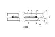
- FIG. 2 shows a cross section of the terminal 26 in the vertical direction along the straight line MM.
- FIG. 3 shows a cross section of the terminal 16 in the lateral direction along the straight line NN.
- the detailed shape of the corner P where the vicinity of the notch 12b of the upper substrate 10 and the vicinity of the notch 22b of the lower substrate 20 intersect will be described with reference to FIG. Further, the four corners of the liquid crystal panel 1 including P are formed by curved surfaces.
- FIG. 2 schematically shows a cross section of the liquid crystal panel 1 along the MM in FIG. The upper side is the upper substrate 10 and the lower side is the lower substrate 20.
- the liquid crystal 40 is sandwiched between the upper film substrate 12 and the lower film substrate 22, and the liquid crystal 40 is sealed inside by the sealing portion 30 using a sealing agent.
- the left end in this figure corresponds to the bottom side in FIG. 1, and a terminal 26 is formed on the inner surface side of the lower film substrate 22.
- a range indicated by a broken line in the upper part of the terminal 26 is a portion where the upper film substrate 12 is deleted, which is indicated by a broken line 12a in FIG.
- the U-shaped groove provided in the upper film substrate 12 where the notch 12b is formed is the notch 12d.
- the cut 12d is provided with a cut in advance in order to delete the deletion range indicated by the broken line 12a.
- the cut is provided by, for example, a laser processing machine after the upper and lower substrates are bonded together. You may insert with a cutter (cutter). Then, along the notch 12d, a part of the upper film substrate 12 is deleted by machine or manual work to form the notch 12b.
- the cut is provided to an appropriate depth of the film substrate in accordance with the deletion operation.
- the reason for making the cut in advance is that an electrode connected to the terminal 26 is formed on the opposite side of the substrate on which the cut is to be formed, and there is a risk of damaging the terminal directly under the opening operation with a laser or a blade.
- FIG. 3 schematically shows a cross section of the liquid crystal panel 1 along NN in FIG.
- the upper side is the upper substrate 10 and the lower side is the lower substrate 20.
- the right end in this figure corresponds to the right side of FIG. 1, and the terminal 16 is formed on the inner surface side of the upper film substrate 12.
- a range indicated by a broken line below the terminal 16 is a portion where the lower film substrate 22 indicated by a broken line 22a in FIG.
- the lower film substrate 22 is provided with a U-shaped cut 22d from the back surface.
- the method of providing the cut 22d is the same as that of the cut 12d described above.
- a part of the lower film substrate 22 is deleted by machine or manual work to form a notch 22b.
- a plurality of liquid crystal panels are made by laminating a large mother substrate and cut out from the liquid crystal panels to produce individual liquid crystal panels. That is, the step of FIG. 1A is performed on a large mother substrate. A plurality of transparent electrodes, terminals, and the like are collectively formed on a large-sized lower film substrate, and each of the sealing portions 30 is printed or applied on the mother substrate, and the liquid crystal is dropped. An upper film substrate of a size (a plurality of transparent electrodes, terminals and the like are collectively formed as in the lower film substrate) is bonded. And it cuts out from the aggregate
- the timing of cutting the surface of the film substrate with a laser or the like may be provided in the state of the mother substrate (before cutting), or may be provided collectively, or after cutting into each liquid crystal panel 1 Either is acceptable.
- the process of providing the notches 12b and 22b along the cuts 12d and 22d is performed manually, it is performed after cutting into individual liquid crystal panels.
- the process of providing the notches 12b and 22b is a mechanical process, the process may be performed in the state of a mother board.
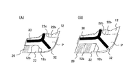
- FIG. 4 is an enlarged view showing the corner P of FIG. 1 (C).
- the corner 12c of the notch 12b of the upper film substrate 12 is formed with a curved surface.
- the opposite side (left side) not shown is formed with a curved surface.
- the opposite side (upper side) not shown is the same.
- corner P where the side where the terminal of the upper substrate 10 is provided and the side where the terminal of the lower substrate 20 is provided is also formed with a curved surface. The occurrence of chipping can be suppressed when the corner portion P is hit.
- the deletion work is facilitated by providing curved surfaces at the corners 12c and 22c.
- the reinforcing portion 32 by the sealing agent is provided in the intersecting corner region, and the upper film substrate 12 and the lower film substrate 22 are bonded by the sealing agent, so that the strength of the corner portion is increased.
- the strength at the corner portion P is reduced by the notch provided in the vicinity, the strength reduction can be compensated by bonding.
- FIG. 4B shows an example in which the corner 12c of the notch 12b and the corner 22c of the notch 22b are formed not at a curved surface but at a right angle. Although it is more desirable to make the corner a curved surface in terms of erasing workability and preventing stress concentration when an external force is applied to the corner, it is not limited to a curved surface.
- FIG. 5 is a diagram illustrating a state in which a wiring member is connected to the liquid crystal panel 1.
- wiring members 60 are connected to the terminals 26 exposed from the bottom side of the lower substrate 20 to the front surface side and the terminals 16 exposed from the right side of the upper substrate 10 to the back side, respectively.
- As the wiring member 60 a flexible cable generally rich in flexibility is used.
- the terminals 16 and 26 and the terminals of the wiring member 60 are joined by pressure bonding.
- a driver IC 70 for driving liquid crystal is also mounted on the wiring member 60.
- the wiring member 60 is connected to a CPU or the like of a device in which the liquid crystal panel 1 is incorporated.
- FIG. 6 is a diagram showing an example of the shape of the reinforcing portion 32 provided at the corner portion P.
- angular part P is assumed variously, some typical examples are introduced in FIG. First, FIG. 6A shows an example in which the reinforcing portion 32 is not provided at the corner portion P. When it is not necessary to bond the upper and lower film substrates at the corner portion P, the reinforcing portion 32 is not provided. This is because the corner portion P is not a single plate as shown in FIG. 8 but is composed of two plates, so that the strength may be sufficient without bonding.
- FIG. 6B shows a shape similar to that of the reinforcing portion 32 shown in FIG.
- the shape of the reinforcing portion 32 is formed by a single line that extends radially from the corner portion of the sealing portion 30 surrounding the liquid crystal 40 to the corner portion P. By bonding the corner portion P, it is more resistant to chipping compared to FIG.
- FIG. 6C shows a case where the shape of the reinforcing portion 32 is two lines.
- the shape of the reinforcing part 32 is formed by two lines that radiate from the square corners surrounding the liquid crystal 40 toward the corners P. Compared with the case of one, the adhesive strength between the upper film substrate 12 and the lower film substrate 22 is increased.
- FIG. 6D shows a case where the shape of the reinforcing portion 32 is formed by two lines along the notch portion 12b and the notch portion 22b.
- the shape of the reinforcing part 32 is formed by a line having a shape along the side of the notch 12b and a line having a shape along the side of the notch 22b. Since adhesion is performed in the vicinity of the notches 12b and 22b, the upper film substrate 12 or the lower film substrate 22 is further prevented from being peeled off from the notches.
- FIG. 6E shows the case where the shape of the reinforcing portion 32 is the entire area of the corner portion P. Since the entire corner portion P is bonded, the upper film substrate 12 or the lower film substrate 22 is further prevented from being peeled from the cutout portion.
- FIG. 7 is a diagram showing an example of a rectangular liquid crystal panel 1 in which terminals are provided in four directions.
- the liquid crystal panel 1 shown in FIG. 1 an example is shown in which terminals are provided on two adjacent sides of the upper substrate 10 and the lower substrate 20.
- terminals are provided on the left and right sides of the upper substrate 10 and terminals are provided on the upper and lower sides of the lower substrate 20, respectively.
- Notch portions are respectively provided on the corresponding upper and lower sides of the upper film substrate 12 so that the terminals on the upper and lower sides of the lower film substrate 22 are exposed.
- notches are provided on the corresponding left and right sides of the lower film substrate 22 so as to expose the terminals of the upper film substrate 12.
- a region surrounded by a two-dot chain line indicates a display region 50.
- the terminals shown in FIG. 1 are combined into one, this figure shows an example in which the terminals are divided into a plurality of parts.
- the terminal is divided into three, and in the lower film substrate 22, the terminal is divided into two.
- the notch portion is shown as being formed as one piece, but the notch portion may be formed separately for each terminal.
- each corner is provided with a reinforcing portion 32 similar to that in the example of FIG. In this way, even when terminals are provided on all four sides, the four corners of the liquid crystal panel 1 are all formed of two plates and are formed of curved surfaces, so that the strength against chipping can be increased. it can.
- the intersecting corner may be formed with a slope of about 45 degrees instead of a curved surface.
- the reinforcement part does not need to be continuously formed from the sealing agent for enclosing. That is, they may be separated.
- the adhesive for the reinforcing portion is not necessarily limited to the sealing agent, and may be a material different from the sealing agent. Further, it is not always necessary to provide the reinforcing portions at all the corner portions (four locations if a rectangular substrate).
- the liquid crystal panel is not limited to a square (square) shape. A polygon such as a pentagon or a part thereof may be a curved surface. 4) There is no limitation that the number of sides on which the terminals are provided is the same on the upper and lower substrates.
Landscapes
- Physics & Mathematics (AREA)
- Nonlinear Science (AREA)
- Mathematical Physics (AREA)
- Chemical & Material Sciences (AREA)
- Crystallography & Structural Chemistry (AREA)
- General Physics & Mathematics (AREA)
- Optics & Photonics (AREA)
- Liquid Crystal (AREA)
- Engineering & Computer Science (AREA)
- Manufacturing & Machinery (AREA)
- Devices For Indicating Variable Information By Combining Individual Elements (AREA)
Description
本発明は、液晶パネルに関し、特に端子付近での液晶パネルの強度を向上させる技術に関する。
ドットマトリクスを表示する液晶パネルは、方形状(四角)の形状で、電極付の2枚の透明基板をこの電極を内側にして上下で対向させて、その間に液晶が封入される。外部に繋がれる電気配線に接続される端子が、上下基板の少なくとも1枚の辺縁部に設けられる。端子は基板内面の透明電極と連続するので、端子も基板の内側の面に設けられる。
図8を用いて、端子を露出されるために対向する基板の一部を削除する処理を説明する。図8(A)は、上基板110と下基板120を分離して示したものである。上基板110と下基板120は、透明基板で外観寸法が同一である。上基板110のベースになる上フィルム基板112の下基板120と対向する面に透明電極114が形成される。下基板120のベースになる下フィルム基板122の上基板110と対向する面にも、透明電極124が形成される。上基板110と下基板120の間には、液晶を内部に封入するためのシール剤130が、外周に沿った経路に設けられる。シール剤130は、上基板110と下基板120を結合する接着剤でもある。水平方向に並んで配列された電極114の右辺の部分が、上基板110での端子116となる。垂直方向に並んで配列された電極124の底辺部分が、下基板120での端子126となる。
図8(B)は、内部に液晶が封入され、シール剤によって上基板110と下基板120が結合された状態を示す図である。上基板110での端子となる右辺の部分は、直下に対向する下基板120があり、この下基板120により遮蔽されている。下基板120での端子となる底辺の部分は、真上に対向する上基板110があり、この上基板110により遮蔽されている。端子116を遮蔽する下基板120の領域を122aで示す。端子126を遮蔽する上基板110の領域を112aで示す。
なお、液晶パネルを、大きなマザー基板で作成された複数の液晶パネルの集合体から、切り出して製造されるという理由から、フィルム基板を予め端子を遮蔽しないような形状にすること困難であるという事情がある。
図8(C)は、端子を遮蔽している部分が削除された状態を示す図である。下基板120の端子126を露出させるために、上基板110では、破線112bから下の部分が削除される。同様に、下基板120では、破線122bから右の部分が削除される。この処理により、上基板110の端子116が右辺に露出され(裏面から見て)、下基板120の端子126が底辺に露出される。また、液晶パネルの右隅の角部は、上基板110と下基板120で削除した部分が重なるために、切りかかれて、拡大して示すように階段状になってしまう。
また、液晶パネルの端子に関しては、基板の1辺に切欠き部を形成して、この切欠き部にフレキシブル基板と接続される端子を設けた提案もある(例えば特許文献1)。
液晶パネルの角部は、液晶パネルの組み立て作業中の取り扱いによって壊れやすいので、取り扱いに注意が必要になる。そして、図8で示した状態の液晶パネルでは、それぞれ片面が削除された底辺と右辺が交差する部分(右下隅)が階段状の形状となり、この部分は組立て等のハンドリング時に引っかかりやすい。また、交差する部分は基板の片方が削除されて単基板状態となるため、強度も低下し欠けやすくなる。液晶パネルの端子を露出させるためには、対向する基板の一部を切除し開放して切欠きを設けることが必要になるが、切除し切欠きを設けても基板の角部の強度が低下しないような液晶パネルが求められる。
本願発明は、上記課題に鑑み、基板の片側を切除し切り欠きを設けても基板の角部の強度が低下しない液晶パネルを提供することを目的とする。
上記目的を達成するために、方形状の1対の透明基板を貼り合わせてなる液晶パネルにおいて、それぞれ電極が供えられた面を内側にして間に液晶を挟んで貼り合わされる透明な2枚の基板と、上記2枚の基板の内側の少なくも各1辺であって、相異なる関係の辺にそれぞれ設けられ、上記電極に接続されて当該液晶パネルへの配線部材が取り付られる端子と、備え相手側の端子に対向する上記2枚の基板の各辺には、当該辺の両端にあたる両角部を残して、相手側の端子を露出させる切欠きが設けられ、上記辺の両角部が、曲面または斜面で形成される。
本発明によれば、切欠きを設けても基板の角部の強度が低下しない液晶パネルを提供することができる。
以下、図面に従って本発明の実施形態を説明する。図1は、本発明の実施形態に係る液晶パネル1の構成を示す図である。液晶パネル1として、ドットマトリクスを表示するタイプで説明する。
液晶パネル1は、上基板10と下基板20と封止部30及び液晶40を有する。上基板10と下基板20の一方がCOM(コモン)基板で、他方がSEG(セグメント)基板である。図1(A)は、上基板10と下基板20が貼り合わせされる前の状態を示す。上基板10は、透明な上フィルム基板12と、上フィルム基板12の内側の面(本図では裏側)に形成される透明電極14と、透明電極14の延長上に形成される端子16(本図では裏側)を有する。
同様に下基板20は、透明な下フィルム基板22と、下フィルム基板22の内側の面(本図では表側)に形成される透明電極24と、透明電極24の延長上に形成される端子26を有する。端子26は、端子16が設けられた辺と隣接する関係にある対向基板の辺に設けられている。
上フィルム基板12、下フィルム基板22は、樹脂製のフィルムで、例えばポリエチレンテレフタレート(PET)、あるいはポリカーボネイト(PC)等のフィルムからなる。また、上フィルム基板12と下フィルム基板22の外寸は、同一である。
透明電極14、24は、各フィルム基板上に微細間隔でパターニングされた帯状の走査電極が並列に配置された電極層である(例えば、0.175mmピッチの1024本)。透明電極の形成材料としては、例えばインジューム錫酸化物(ITO)が代表的であるが、その他インジューム亜鉛酸化物(IZO)等の透明電極膜、アルミニューム又はシリコン等の金属電極、又はアモルファスシリコン等の光導電性膜等を用いることが出来る。上基板10の透明電極14は、水平方向に直線的に形成される。下基板20の透明電極24は、透明電極14に対し垂直方向に直線的に形成される。
また、上フィルム基板12と下フィルム基板22には、透明電極14、24の上に配向膜がコーティングされる。配向膜は、機能膜として液晶分子の配列を制御するためのものである。
下基板20の外周に沿って1周するように、封止部30が設けられる。封止部30は、注入された液晶を内部に封入するものである。封止部30は、シール剤により形成される。シール剤は、紫外線硬化型あるいは熱硬化型がある。封止部30は、印刷処理またはディスペンサーによる塗布処理によりシール剤を下フィルム基板22表面に塗布することで、形成される。封止部30は、フィルム基板12、22を接着する接着剤でもある。
封止部30は、液晶を内部に封入するように下基板20の外形よりやや内側に沿って略矩形に形成される。さらにこの矩形の部分から、下基板20の左下、右下、右上の3箇所に延びるように形成される。延びた部分は、上下基板の角部を補強する補強部32となる。
また、端子16は上フィルム基板12の内面の右辺縁部に設けられる。端子16は、透明電極14の延長上で、貼り合せられた後に封止部30の外側となる領域に設けられる。同様に、端子26は下フィルム基板22の底辺の辺縁部に設けられる。端子26は、透明電極24の延長上で、封止部30の外側の領域に設けられる。
図1(B)は、内部に液晶が注入され封止部30によって上基板10と下基板20とが貼り合わされた状態の液晶パネル1を示す図である。シール剤による補強部32によって、左下、右下、右上の角部3箇所でも、上下基板が接着される。上フィルム基板12の端子16の部分は、下フィルム基板22によって遮蔽され、下フィルム基板22の端子26の部分も、上フィルム基板12によって遮蔽されている。各端子を露出させるために、端子の上部を覆っている基板の一部を削除することが必要になる。破線12aで示される水平方向に長い範囲が、端子26を露出させるための上フィルム基板12の削除範囲である。破線22aで示される縦長の範囲が、端子16を露出させるための下フィルム基板22の削除範囲である。
図1(C)は、破線12aで示される削除範囲と破線22aで示される削除範囲が、それぞれ削除された状態の液晶パネル1を示す図である。上フィルム基板12で削除された部分が切欠き12bとなる。下フィルム基板22で削除された部分が切欠き22bとなる。切欠き22bは、上フィルム基板12を透過して示される。なお、2点鎖線で囲まれた領域は、表示領域50を示す。
切欠き12bの範囲に端子26が露出される。切欠き22bの範囲に端子16が露出される。端子16は裏面側に露出される。また、切欠き12bの左右の隅12cは、R面(曲面)で形成される。切欠き22bの上下の隅22cも、R面(曲面)で形成される。
さらに、端子26につき、直線MMに沿って縦方向で断面したものを図2に示す。また、端子16につき、直線NNに沿って横方向で断面したものを図3に示す。また、上基板10の切欠き部12bの近傍と下基板20の切欠き部22bの近傍が交差する角部Pの詳細形状については図4で説明する。また、Pを含む液晶パネル1の4つの角部は、曲面で構成される。 図2は、図1(C)のMMに沿った液晶パネル1の断面を模式的に示すものである。上側が上基板10で、下側が下基板20である。上フィルム基板12と下フィルム基板22の間に液晶40が挟まれ、シール剤による封止部30によって液晶40は内部に封止される。本図での左端が図1の底辺側に相当し、下フィルム基板22の内面側に端子26が形成される。端子26の上部で破線で示す範囲が、図1(B)の破線12aで示した上フィルム基板12の削除された部分である。
切欠き12bが形成される上フィルム基板12に設けられたU字状の溝が、切り込み12dである。切り込み12dは破線12aで示される削除範囲を削除するために、予め切り込みが設けられる。切り込みは、上下基板が貼り合わされた後に、例えばレーザー加工機によって設けられる。刃物(カッター)で入れても良い。そして、切り込み12dに沿って、上フィルム基板12の一部を機械または手作業で削除して、切欠き部12bが形成される。切り込みは、削除作業に合わせてフィルム基板の適当な深さまで設けられる。予め切り込みを入れる理由は、切り込みが形成される基板の対面側に端子26に繋がる電極が形成されており、レーザー又は刃物による開口作業で直下にある端子を損傷するおそれがあるからである。
図3は、図1(C)のNNに沿った液晶パネル1の断面を模式的に示すものである。図3と同様に、上側が上基板10で、下側が下基板20である。本図での右端が図1の右辺側に相当し、上フィルム基板12の内面側に端子16が形成される。端子16の下部で破線で示す範囲が、図1(B)の破線22aで示した下フィルム基板22の削除された部分である。
上下基板が貼り合わされた後に、下フィルム基板22に裏側の面からU字状の切り込み22dが設けられる。切り込み22dを設ける方法は、上述した切り込み12dの場合と同様である。そして、切り込み22dに沿って、下フィルム基板22の一部を機械または手作業で削除して、切欠き部22bが形成される。
また、液晶パネル1を量産する場合には、大きなマザー基板を貼り合わせて複数の液晶パネルをまとめて作り、これから切り出して個々の液晶パネルが生産される。つまり、図1(A)の段階は、大きなマザー基板で行われる。大きなサイズの下フィルム基板に複数個分の透明電極や端子等をまとめて形成し、このマザー基板上にそれぞれ封止部30を印刷または塗布して設けて、液晶を滴下してから、同じく大きなサイズの上フィルム基板(下フィルム基板同様に複数個分の透明電極や端子等をまとめて形成している)を貼り合せる。そして、液晶パネルの集合体から、個々の液晶パネルに切り出す。
ここで、フィルム基板の面にレーザー等で切り込みを入れるタイミングは、マザー基板の状態(切り出す前)で、まとめて切り込みを設けるようにしてもよいし、あるいは個々の液晶パネル1に切り出した後のいずれでもよい。そして、切り込み12d、22dに沿って、切欠き部12b、22bを設ける処理を手作業で行う場合には、個々の液晶パネルに切り出した後に行う。ただし、切欠き部12b、22bを設ける処理が機械処理の場合には、マザー基板の状態で行うようにしてもよい。
図4は、図1(C)の角部Pを拡大して示す図である。図4(A)は、図1(C)で示したように、上フィルム基板12の切欠き部12bの隅部12cを曲面で形成したものである。図示していない反対側(左側)も同じである。下フィルム基板22の切欠き部22bの隅部22cも同様に曲面で形成される。図示していない反対側(上側)も同じである。これにより、角部P等に外力が加わった場合に、隅部に発生する応力集中が緩和される。
また、上基板10の端子が設けられた辺と下基板20の端子が設けられた辺が交差する角部Pも、曲面で形成される。角部Pをぶつけた場合に、欠けの発生を抑えることができる。
また、切欠き12b、26bを削除する場合、隅部12c,22cに曲面を設けることで削除作業の容易となる。
また、交差する角部の領域には、シール剤による補強部32が設けられて、上フィルム基板12と下フィルム基板22がシール剤によって接着されるので、この角部の強度は増す。近傍に設けられた切欠きによって角部Pでの強度が低下するが、接着されることで、強度低下を補うことができる。
図4(B)は、切欠き部12bの隅部12cと切欠き部22bの隅部22cが、曲面ではなく直角に形成された例である。隅部を曲面にした方が、削除作業性や角部に外力が加わった時に応力集中を防ぐ点でより望ましいが、曲面に限定するものではない。
図5は、液晶パネル1に配線部材が接続された様子を示す図である。液晶パネル1で、下基板20の底辺から表面側に露出される端子26と 上基板10の右辺から裏面側に露出される端子16に、それぞれ配線部材60が接続される。配線部材60としては、一般に柔軟性に富むフレキシブルケーブルが用いられる。端子16及び端子26と、配線部材60の端子は、圧着によって接合される。また、配線部材60には、液晶を駆動するドライバIC70も実装される。配線部材60は、液晶パネル1を組み込む機器のCPU等に接続される。
図6は、角部Pに設けられた補強部32の形状例を示す図である。角部Pにおける補強部32の形状は、様々想定されるが、図6で代表例をいくつか紹介する。まず図6(A)は、角部Pに補強部32を設けない例である。角部Pで上下のフィルム基板を接着する必要がない場合には、補強部32を設けない。角部Pが、図8で示したような単板ではなく2枚板で構成されるので、接着しなくても強度が十分の場合もあるからである。
図6(B)は、図1で示した補強部32と同様な形状を示すものである。補強部32の形状が、液晶40を囲む封止部30の角の部分から角部Pに放射状に向かう1本のラインで、形成される。角部Pが接着されることで、図6(A)に比べてさらに欠けに強くなる。
図6(C)は、補強部32の形状が2本のラインの場合を示すものである。補強部32の形状が、液晶40を囲む方形状の角の部分から角部Pに放射状に向かう2本のラインで、形成される。1本の場合に比べて、上フィルム基板12と下フィルム基板22間の接着強度が高まる。
図6(D)は、補強部32の形状が、切欠き部12bと切欠き部22bに沿うような2本のラインで形成した場合を示すものである。補強部32の形状が、切欠き部12bの側部に沿うような形状のラインと切欠き部22bの側部に沿うような形状のラインで、形成される。切欠き部12b、22bのより近傍で接着されるので、上フィルム基板12または下フィルム基板22が切欠き部から剥離されることがさらに防止される。
図6(E)は、補強部32の形状が、角部Pの全体領域の場合を示すものである。角部P全体が接着されるので、上フィルム基板12または下フィルム基板22が切欠き部から剥離されることがより防止される。
図7は、4方向に端子が設けられる方形の液晶パネル1の例を示す図である。図1で示した液晶パネル1では、上基板10と下基板20とで隣接する2辺に端子が設けられた例を示した。ここでは、上基板10の左右辺にそれぞれ端子が設けられ、下基板20の上下辺にそれぞれ端子が設けられた例を示す。下フィルム基板22の上下辺の端子を露出させるように、上フィルム基板12の対応する上下の辺には、それぞれ切欠き部が設けられる。同様に、上フィルム基板12の端子を露出させるように、下フィルム基板22の対応する左右の辺には、それぞれ切欠き部が設けられる。なお、2点鎖線で囲まれた領域は、表示領域50を示す。
また、端子も、図1では1つにまとめられたものを示したが、本図では、複数に分割して配列された例で示す。上フィルム基板12では、端子は3つに分割、下フィルム基板22では、端子は2つに分割されている。また、本図では、切欠き部は、1つにまとめて形成されたものを示すが、切欠き部も、各端子ごとに分けて形成するようにしてもよい。また、図示はしないが、各角部には、図1の例と同様な補強部32を設けることで、欠けに対して強くなる。このように、4辺全てに端子が設けられる場合も、液晶パネル1の4つの角部が全て2枚板で構成され、かつ曲面で形成することで、欠けに対して強度を強くすることができる。
以上の実施形態から、少なくとも以下の効果が奏される。
1)液晶パネルの外周をR面で構成したので、パネルのハンドリング時の引っかかりが防止でき、パネルの角部に欠けが発生することを防止できる。
2)切欠きが設けられても、液晶パネルの角部では2枚重なった状態なので、落下時の液晶パネルコーナ(角部)の強度の低下を防止できる。
3)液晶パネルの角部に封止用のシール剤を塗布して、角部で上下基板を接着したので、角部における強度が増す。また、切欠きが設けられた辺に対応する角部であるかを問わずに、液晶パネルの4角全てにシール剤を塗布すれば、さらに強度が増す。
4)端子のための開口である切欠きの隅部を、R付(U字)形状にしたので、削除作業が容易になる。
1)液晶パネルの外周をR面で構成したので、パネルのハンドリング時の引っかかりが防止でき、パネルの角部に欠けが発生することを防止できる。
2)切欠きが設けられても、液晶パネルの角部では2枚重なった状態なので、落下時の液晶パネルコーナ(角部)の強度の低下を防止できる。
3)液晶パネルの角部に封止用のシール剤を塗布して、角部で上下基板を接着したので、角部における強度が増す。また、切欠きが設けられた辺に対応する角部であるかを問わずに、液晶パネルの4角全てにシール剤を塗布すれば、さらに強度が増す。
4)端子のための開口である切欠きの隅部を、R付(U字)形状にしたので、削除作業が容易になる。
また、上記説明した実施形態につき、以下の変形が可能である。
1)交差する角部を曲面ではなく45度程度の斜面で形成してもよい。
2)補強部は、封入するためのシール剤から連続的に形成されたものでなくともよい。つまり分離されていてもよい。また、補強部の接着剤は、シール剤に限定される必要はなく、シール剤と異なる材質であってもよい。また、補強部は、必ずしも角部の全て(四角形の基板であれば、4箇所)に設ける必要はない。
3)液晶パネルは、方形状(四角)の形状に、制限されるものではない。5角等多角形あるいは、一部が曲面であってもよい。
4)端子が設けられる辺は、上下基板で同数である制限はない。
1)交差する角部を曲面ではなく45度程度の斜面で形成してもよい。
2)補強部は、封入するためのシール剤から連続的に形成されたものでなくともよい。つまり分離されていてもよい。また、補強部の接着剤は、シール剤に限定される必要はなく、シール剤と異なる材質であってもよい。また、補強部は、必ずしも角部の全て(四角形の基板であれば、4箇所)に設ける必要はない。
3)液晶パネルは、方形状(四角)の形状に、制限されるものではない。5角等多角形あるいは、一部が曲面であってもよい。
4)端子が設けられる辺は、上下基板で同数である制限はない。
なお、本発明は上述した実施形態そのままに限定されるものではく、実施段階でのその要旨を逸脱しない範囲で構成要素を変形して具体化することができる。また、上記実施形態に開示されている複数の構成要素の適宜な組み合わせにより、種々の発明を形成することができる。例えば、実施形態に示される全構成要素を適宜組み合わせても良い。さらに、異なる実施形態にわたる構成要素を適宜組み合わせてもよい。このような、発明の趣旨を逸脱しない範囲内において種々の変形や応用が可能であることはもちろんである。
1 液晶パネル
10 上基板
12 上フィルム基板
12b 切欠き部
12c 隅部
12d 切り込み
14 透明電極
16 端子
20 下基板
22 下フィルム基板
24 透明電極
26 端子
30 封止部
32 補強部
40 液晶
50 表示領域
60 配線部材
70 ドライバIC
10 上基板
12 上フィルム基板
12b 切欠き部
12c 隅部
12d 切り込み
14 透明電極
16 端子
20 下基板
22 下フィルム基板
24 透明電極
26 端子
30 封止部
32 補強部
40 液晶
50 表示領域
60 配線部材
70 ドライバIC
Claims (7)
- 方形状の1対の透明基板を貼り合わせてなる液晶パネルにおいて、
それぞれ電極が供えられた面を内側にして間に液晶を挟んで貼り合わされる透明な2枚の基板と、
上記2枚の基板の内側の少なくも各1辺であって、相異なる関係の辺にそれぞれ設けられ、上記電極に接続されて当該液晶パネルへの配線部材が取り付られる端子と、備え
相手側の端子に対向する上記2枚の基板の各辺には、当該辺の両端にあたる両角部を残して、相手側の端子を露出させる切欠きが設けられ、
上記辺の両角部が、曲面または斜面で形成される
ことを特徴とする液晶パネル。 - 上記2枚の基板の各端子は、当該2枚の基板の隣接する関係となる辺にそれぞれ設けられる
ことを特徴とする請求項1に記載の液晶パネル。 - 上記2枚の基板は、上記角部において接着剤によって貼り合わされる
ことを特徴とする請求項1に記載の液晶パネル。 - 上記接着剤は、液晶を内部に封止するシール材である、
ことを特徴とする請求項3に記載の液晶パネル。 - 上記基板は、樹脂製のフィルムである
ことを特徴とする請求項1に記載の液晶パネル。 - 上記切欠きは、上記各辺から内側へえぐるように形成され、当該えぐられた部分の隅部を曲面で形成した
ことを特徴とする請求項1に記載の液晶パネル。 - 方形状の形状で、それぞれ電極が供えられた面を内側にして間に液晶を挟んで貼り合わされる透明な2枚の基板と、上記2枚の基板の内側の少なくも各1辺であって、相異なる関係の辺に上記電極に接続されて当該液晶パネルへの配線部材が取り付られる端子とを有する液晶パネルを、大きなサイズのマザー基板により作成される液晶パネルの集合体から、切り出して製造する液晶パネルの製造方法において、
上記切り出される前の上記液晶パネルの集合体の状態で、切り出した後の各液晶パネルで各端子を遮蔽することとなる範囲について、上記マザー基板に対して、まとめて切り込みを形成し、
上記マザー基板から上記液晶パネルを切り出して、
上記切り出した液晶パネルの基板の一部を上記切り込みに沿って削除して、上記切り出した液晶パネルの基板に上記端子を露出させるための切欠きを形成する
ことを特徴とする液晶パネルの製造方法。
Priority Applications (2)
| Application Number | Priority Date | Filing Date | Title |
|---|---|---|---|
| PCT/JP2012/056002 WO2013132633A1 (ja) | 2012-03-08 | 2012-03-08 | 液晶パネル |
| TW102100119A TW201337387A (zh) | 2012-03-08 | 2013-01-03 | 液晶面板 |
Applications Claiming Priority (1)
| Application Number | Priority Date | Filing Date | Title |
|---|---|---|---|
| PCT/JP2012/056002 WO2013132633A1 (ja) | 2012-03-08 | 2012-03-08 | 液晶パネル |
Publications (1)
| Publication Number | Publication Date |
|---|---|
| WO2013132633A1 true WO2013132633A1 (ja) | 2013-09-12 |
Family
ID=49116148
Family Applications (1)
| Application Number | Title | Priority Date | Filing Date |
|---|---|---|---|
| PCT/JP2012/056002 Ceased WO2013132633A1 (ja) | 2012-03-08 | 2012-03-08 | 液晶パネル |
Country Status (2)
| Country | Link |
|---|---|
| TW (1) | TW201337387A (ja) |
| WO (1) | WO2013132633A1 (ja) |
Cited By (3)
| Publication number | Priority date | Publication date | Assignee | Title |
|---|---|---|---|---|
| WO2016190240A1 (ja) * | 2015-05-27 | 2016-12-01 | シャープ株式会社 | 表示パネルの製造方法 |
| CN110189631A (zh) * | 2018-02-23 | 2019-08-30 | 三星显示有限公司 | 显示设备 |
| CN110928008A (zh) * | 2019-11-26 | 2020-03-27 | 深圳市华星光电半导体显示技术有限公司 | 一种面板切割装置 |
Citations (4)
| Publication number | Priority date | Publication date | Assignee | Title |
|---|---|---|---|---|
| JPH0682805A (ja) * | 1992-08-31 | 1994-03-25 | Ricoh Co Ltd | 液晶表示素子およびその製造方法 |
| JP2003223111A (ja) * | 2002-01-30 | 2003-08-08 | Seiko Epson Corp | 表示装置の製造方法、表示装置の封止側原型基板、表示装置の集合体、表示装置および電子機器 |
| JP2004118135A (ja) * | 2002-09-30 | 2004-04-15 | Hitachi Ltd | 液晶表示装置の製造方法及びガラス切断装置 |
| JP2008046446A (ja) * | 2006-08-18 | 2008-02-28 | Epson Imaging Devices Corp | 電気光学装置、電子機器、および電気光学装置の製造方法 |
-
2012
- 2012-03-08 WO PCT/JP2012/056002 patent/WO2013132633A1/ja not_active Ceased
-
2013
- 2013-01-03 TW TW102100119A patent/TW201337387A/zh unknown
Patent Citations (4)
| Publication number | Priority date | Publication date | Assignee | Title |
|---|---|---|---|---|
| JPH0682805A (ja) * | 1992-08-31 | 1994-03-25 | Ricoh Co Ltd | 液晶表示素子およびその製造方法 |
| JP2003223111A (ja) * | 2002-01-30 | 2003-08-08 | Seiko Epson Corp | 表示装置の製造方法、表示装置の封止側原型基板、表示装置の集合体、表示装置および電子機器 |
| JP2004118135A (ja) * | 2002-09-30 | 2004-04-15 | Hitachi Ltd | 液晶表示装置の製造方法及びガラス切断装置 |
| JP2008046446A (ja) * | 2006-08-18 | 2008-02-28 | Epson Imaging Devices Corp | 電気光学装置、電子機器、および電気光学装置の製造方法 |
Cited By (6)
| Publication number | Priority date | Publication date | Assignee | Title |
|---|---|---|---|---|
| WO2016190240A1 (ja) * | 2015-05-27 | 2016-12-01 | シャープ株式会社 | 表示パネルの製造方法 |
| US10317713B2 (en) | 2015-05-27 | 2019-06-11 | Sharp Kabushiki Kaisha | Method of producing display panels |
| CN110189631A (zh) * | 2018-02-23 | 2019-08-30 | 三星显示有限公司 | 显示设备 |
| CN110189631B (zh) * | 2018-02-23 | 2022-08-19 | 三星显示有限公司 | 显示设备 |
| CN110928008A (zh) * | 2019-11-26 | 2020-03-27 | 深圳市华星光电半导体显示技术有限公司 | 一种面板切割装置 |
| CN110928008B (zh) * | 2019-11-26 | 2022-05-31 | 深圳市华星光电半导体显示技术有限公司 | 一种面板切割装置 |
Also Published As
| Publication number | Publication date |
|---|---|
| TW201337387A (zh) | 2013-09-16 |
Similar Documents
| Publication | Publication Date | Title |
|---|---|---|
| JP4494446B2 (ja) | 表示装置 | |
| EP2520968B1 (en) | Display apparatus having chamfered edges | |
| EP3674782A1 (en) | Substrate, manufacturing method therefor, display panel, manufacturing method therefor, and tiled screens | |
| US9684404B2 (en) | Display device | |
| US10459265B2 (en) | Display device | |
| CN205353529U (zh) | 液晶显示装置 | |
| WO2012147672A1 (ja) | 表示モジュール及び表示装置 | |
| TWI521286B (zh) | 薄化顯示面板及其製造方法 | |
| CN105938267A (zh) | 显示装置及其制造方法 | |
| KR20160065404A (ko) | 디스플레이 장치와, 이의 제조 방법 | |
| WO2015170678A1 (ja) | 粘着部材、粘着部材の製造方法、及び貼り合わせ部材の製造方法 | |
| JP2010097118A (ja) | 液晶表示装置および電子機器 | |
| JP5160687B2 (ja) | 表示パネル、表示装置及びその製造方法 | |
| CN106997126A (zh) | 显示装置 | |
| US20180004053A1 (en) | Display device | |
| JP2016126041A (ja) | 表示装置 | |
| JP4896619B2 (ja) | 表示装置 | |
| WO2013132633A1 (ja) | 液晶パネル | |
| JP2019101224A (ja) | 表示装置 | |
| US11719970B2 (en) | Display device and method of manufacturing the same, electronic equipment and method of manufacturing the same, and backlight unit | |
| JP5218262B2 (ja) | 表示パネルとそれを用いる表示モジュール | |
| JP6483388B2 (ja) | 液晶表示装置 | |
| JP2019032410A (ja) | 表示装置 | |
| US20150156897A1 (en) | Display device | |
| JP2007298747A (ja) | 表示パネルの製造方法および表示パネル |
Legal Events
| Date | Code | Title | Description |
|---|---|---|---|
| 121 | Ep: the epo has been informed by wipo that ep was designated in this application |
Ref document number: 12870717 Country of ref document: EP Kind code of ref document: A1 |
|
| NENP | Non-entry into the national phase |
Ref country code: DE |
|
| 122 | Ep: pct application non-entry in european phase |
Ref document number: 12870717 Country of ref document: EP Kind code of ref document: A1 |
|
| NENP | Non-entry into the national phase |
Ref country code: JP |