WO2013125591A1 - 評価装置、評価方法、およびデバイス製造方法 - Google Patents
評価装置、評価方法、およびデバイス製造方法 Download PDFInfo
- Publication number
- WO2013125591A1 WO2013125591A1 PCT/JP2013/054202 JP2013054202W WO2013125591A1 WO 2013125591 A1 WO2013125591 A1 WO 2013125591A1 JP 2013054202 W JP2013054202 W JP 2013054202W WO 2013125591 A1 WO2013125591 A1 WO 2013125591A1
- Authority
- WO
- WIPO (PCT)
- Prior art keywords
- pattern
- wafer
- focus
- light
- substrate
- Prior art date
- Legal status (The legal status is an assumption and is not a legal conclusion. Google has not performed a legal analysis and makes no representation as to the accuracy of the status listed.)
- Ceased
Links
Images





Classifications
-
- G—PHYSICS
- G01—MEASURING; TESTING
- G01B—MEASURING LENGTH, THICKNESS OR SIMILAR LINEAR DIMENSIONS; MEASURING ANGLES; MEASURING AREAS; MEASURING IRREGULARITIES OF SURFACES OR CONTOURS
- G01B11/00—Measuring arrangements characterised by the use of optical techniques
-
- G—PHYSICS
- G03—PHOTOGRAPHY; CINEMATOGRAPHY; ANALOGOUS TECHNIQUES USING WAVES OTHER THAN OPTICAL WAVES; ELECTROGRAPHY; HOLOGRAPHY
- G03F—PHOTOMECHANICAL PRODUCTION OF TEXTURED OR PATTERNED SURFACES, e.g. FOR PRINTING, FOR PROCESSING OF SEMICONDUCTOR DEVICES; MATERIALS THEREFOR; ORIGINALS THEREFOR; APPARATUS SPECIALLY ADAPTED THEREFOR
- G03F9/00—Registration or positioning of originals, masks, frames, photographic sheets or textured or patterned surfaces, e.g. automatically
- G03F9/70—Registration or positioning of originals, masks, frames, photographic sheets or textured or patterned surfaces, e.g. automatically for microlithography
- G03F9/7003—Alignment type or strategy, e.g. leveling, global alignment
- G03F9/7023—Aligning or positioning in direction perpendicular to substrate surface
- G03F9/7026—Focusing
Definitions
- the present invention relates to an apparatus and a method for determining a focus state of an exposure apparatus.
- the present invention also relates to a device manufacturing method using this method.
- An exposure apparatus used in a semiconductor manufacturing process performs exposure for one shot on a semiconductor wafer by reducing and projecting a mask pattern provided on a reticle via a mask pattern and a projection lens (projection optical system). It has become.
- the projection optical system is fixed, and the substrate (resist surface on the substrate) on which the pattern is projected is moved in the optical axis direction of the projection optical system (A method of changing the relative positional relationship between the projection optical system and the substrate is an object. This amount of movement in the optical axis direction is called a focus offset, and the focus offset that can obtain the best in-focus state is called the best focus.
- Various methods can be employed as a method for measuring the best focus.
- the present invention has been made in view of such a problem, and an object thereof is to provide an apparatus and a method capable of obtaining the best focus of an exposure apparatus in a short time. Moreover, it aims at providing the device manufacturing method using this method.
- the evaluation apparatus has patterns provided on the surface, respectively, by a plurality of times of projections with different relative positions with respect to the focal position of the projection optical system via the projection optical system.
- An illumination unit that illuminates the substrate, a detection unit that detects illumination light reflected by the surface, and a variation amount of a detection result detected within one projection range is based on the relative position exceeding a predetermined condition.
- the evaluation method according to the present invention illuminates a substrate having a pattern provided on the surface by a plurality of times of projections with different relative positions to the focal position of the projection optical system via the projection optical system, The illumination light reflected on the surface is detected, and the amount of variation in the detection result detected within one projection range is based on the relative position exceeding a predetermined condition. Find the relative position.
- a device manufacturing method is a device manufacturing method including a lithography process in which a pattern is exposed on the surface of a substrate using a projection optical system, and the substrate is manufactured using the evaluation method according to the present invention. And the projection optical system is obtained, the substrate and the projection optical system are adjusted based on the optimum relative position, and a pattern is exposed on the surface of the substrate in the adjusted state.
- the best focus of the exposure apparatus can be obtained in a short time.
- FIG. 1 A surface inspection apparatus is shown in FIG. 1 as an example of an evaluation apparatus according to the present application.
- the surface inspection apparatus 1 of the present embodiment includes a stage 5 that supports a semiconductor wafer 10 (hereinafter referred to as a wafer 10), an illumination system 20, a light receiving system 30, an imaging device 35, an image processing unit 40, and a storage.
- the stage 5 supports the wafer 10 so that a rotation mechanism (not shown) can rotate about the rotational symmetry axis of the wafer 10 (the central axis of the stage 5).
- a rotation mechanism (not shown) can rotate about the rotational symmetry axis of the wafer 10 (the central axis of the stage 5).
- an azimuth angle is defined with reference to a notch center position of a notch provided at the outer peripheral portion or a center position of an orientation flat, and is referred to as a wafer azimuth angle.
- the wafer 10 is transferred from the outside by a transfer device (not shown), placed on the stage 5, and fixed and held on the stage 5 by vacuum suction. Further, the stage 5 is configured to be tiltable together with the wafer 10 as shown by a double arrow in FIG. 1 about an axis Tc passing through the wafer surface parallel to the support surface for supporting the wafer 10 by a tilt mechanism (not shown).
- the incident angle of illumination light can be adjusted.
- the illumination system 20 includes an illumination unit 21 that emits illumination light, and an illumination-side concave mirror 25 that reflects the illumination light emitted from the illumination unit 21 toward the surface of the wafer 10, and is supported by the stage 5. 10 is irradiated with parallel light as illumination light.
- the illumination unit 21 includes a light source unit 22, a light control unit 23, and a light guide fiber 24.
- a metal halide lamp, a mercury lamp, or the like is used.
- the dimming unit 23 includes a bandpass filter and an ND filter, and performs selection and intensity adjustment of light having a predetermined wavelength among the light from the light source unit 22.
- the light guide fiber 24 guides the light from the light control unit 23 to the illumination side concave mirror 25 as illumination light.
- the exit portion of the light guide fiber 24 is disposed on the focal plane of the illumination-side concave mirror 25, and the illumination light is reflected by the illumination-side concave mirror 25 to form a parallel light beam on the surface of the wafer 10 supported by the stage 5. Irradiated. Note that the relationship between the incident angle and the exit angle of the illumination light with respect to the wafer 10 can be adjusted by tilting the stage 5 and changing the mounting angle of the wafer 10.
- an illumination-side polarizing filter 26 is provided between the light guide fiber 24 and the illumination-side concave mirror 25 so that it can be inserted into and removed from the optical path.
- an inspection using diffracted light hereinafter referred to as a diffraction inspection for convenience
- a diffraction inspection for convenience
- an inspection using polarization change in polarization state due to structural birefringence
- PER inspection for convenience
- the light receiving system 30 has a light receiving side concave mirror 31 disposed to face the stage 5 and collects light (reflected light, diffracted light, etc.) emitted from the entire surface of the wafer 10 when irradiated with illumination light. Shine.
- the emitted light collected by the light receiving side concave mirror 31 reaches the imaging surface of the imaging device 35 by an imaging optical system (not shown), and an image of the wafer 10 is formed.
- a light receiving side polarizing filter 32 is provided between the light receiving side concave mirror 31 and the imaging device 35 so as to be inserted into and removed from the optical path.
- the diffraction inspection is performed with the light receiving side polarizing filter 32 removed from the optical path.
- the PER inspection is performed with the light receiving side polarizing filter 32 inserted in the optical path (details of the light receiving side polarizing filter 32 will be described later).
- the imaging device 35 photoelectrically converts the image of the wafer 10 formed on the imaging surface to generate a raw image signal, and sends it to the main control unit 45.
- the main control unit 45 receives the raw image signal sent from the imaging device 35 and sends it to the image processing unit 40.
- the main control unit 45 may be configured to once receive the raw image signal from the imaging device 35 and then send the raw image signal to the image processing unit 40. However, based on an instruction from the main control unit 45, the imaging device 35 The raw image signal may be directly sent to the image processing unit 40. The same applies to the following description.
- the image processing unit 40 generates a digital image of the wafer 10 based on the raw image signal sent from the imaging device 35.
- the digital image of the wafer 10 is sent from the image processing unit 40 to the inspection unit 42 and the evaluation unit 43 by the main control unit 45.
- a digital image of a non-defective wafer is stored in the storage unit 41 in advance, and the inspection unit 42 receives and compares the digital image of the wafer 10 and the digital image of the non-defective wafer to determine defects (abnormality) on the surface of the wafer 10.
- the inspection result by the inspection unit 42 and the digital image of the wafer 10 at that time are output and displayed by the main control unit 45 on an image display device (not shown).
- the inspection result of the wafer 10 and the digital image by the inspection unit 42 may be sent to the storage unit 41 by the main control unit 45 and stored therein.
- the inspection result and the digital image can be output from the output unit 46 to the outside (for example, a semiconductor manufacturing line management system or an exposure apparatus) by the main control unit 45.
- the evaluation unit 43 uses a digital image of the wafer to allow an allowable range of focus offset of the exposure apparatus 101 (a range in which a defect such as a pattern collapse or short circuit does not occur due to defocus) and a best focus (exposure) of the exposure apparatus 101.
- the optimum relative position between the projection optical system of the apparatus and the wafer 10 is obtained (details will be described later).
- the main control unit 45, the evaluation unit 43, the inspection unit 42, the storage unit 41, and the image processing unit 40 can be arranged in the apparatus, but are configured to be able to communicate with each other by wired / wireless communication means. If so, they can be arranged independently of the apparatus.
- at least one of the main control unit 45, the evaluation unit 43, the inspection unit 42, the storage unit 41, and the image processing unit 40 may be disposed in the central monitoring room and communicated via the factory LAN.
- the main control unit 45 controls the operation of the illumination unit 21 and the stage 5 via the hardware control unit 44.
- the hardware control unit 44 controls the light source unit 22 and the light control unit 23 of the illumination unit 21 to adjust the wavelength and intensity of the illumination light. Further, the hardware control unit 44 controls a rotation mechanism unit (not shown) of the stage 5 to adjust the wafer orientation angle. Further, the hardware control unit 44 controls a tilt mechanism (not shown) of the stage 5 to adjust the incident angle and the emission angle of the illumination light.
- a resist film is provided on the uppermost layer of the wafer 10, and a predetermined mask pattern is projected and exposed through the projection optical system by the exposure device 101, and developed by a developing device (not shown).
- the developed wafer 10 is transferred onto the stage 5 from a wafer cassette (not shown) or the developing device by a transfer device (not shown).
- the wafer 10 detects a pattern of the wafer 10 or a reference mark (notch, orientation flat, etc.) on the outer edge.
- the wafer 10 transferred onto the stage 5 is aligned by the rotating mechanism of the stage 5 based on the pattern or reference mark position detected during the transfer.
- a plurality of chip regions (ranges constituting one semiconductor device product) 11 are arranged vertically and horizontally (in the XY directions in FIG. 2).
- a repetitive pattern 12 such as a line pattern or a hole pattern is formed as a semiconductor pattern.
- one shot of exposure includes a plurality of chip areas. In FIG. 2, the area for one chip is set as one shot area for easy understanding. Yes.
- the exposure apparatus 101 is, for example, a step-and-scan exposure apparatus, and is electrically connected to the output unit 46 of the surface inspection apparatus 1 of the present embodiment via a cable or the like.
- the exposure control can be adjusted based on the data (signal).
- the exposure apparatus 101 and the output unit 46 of the surface inspection apparatus 1 do not necessarily have to be electrically connected, and may be configured to be communicable by wired / wireless communication means.
- the illumination side polarizing filter 26 and the light receiving side polarizing filter 32 are removed from the optical path as shown in FIG. Then, the wafer 10 is transferred onto the stage 5.
- the wafer 10 is aligned by placing it at a predetermined position in a predetermined direction by the rotation mechanism of the stage 5.
- the direction of the wafer 10 may be adjusted during the transfer. Due to this alignment, the incident direction of the illumination light on the surface of the wafer 10 and the pattern repetition direction coincide (in the case of a line pattern, perpendicular to the line). Furthermore, when the pitch of the pattern is P, the wavelength of the illumination light applied to the surface of the wafer 10 is ⁇ , the incident angle of the illumination light is ⁇ 1, and the exit angle of the n-th order diffracted light is ⁇ 2, Set tilt to satisfy.
- the hardware control unit 44 controls the light source unit 22 and the light control unit 23 of the illumination unit 21, the tilting mechanism (not shown) of the stage 5, and the like.
- the illumination system 20 irradiates the surface of the wafer 10 with illumination light.
- the light from the light source unit 22 in the illumination unit 21 passes through the dimming unit 23 and has a predetermined wavelength (for example, a wavelength of 248 nm). It is adjusted to the intensity illumination light.
- the adjusted illumination light is emitted from the light guide fiber 24 to the illumination side concave mirror 25, and the illumination light reflected by the illumination side concave mirror 25 is irradiated onto the surface of the wafer 10 as a parallel light flux.
- the diffracted light diffracted by the repetitive pattern on the surface of the wafer 10 is collected by the light-receiving-side concave mirror 31 and reaches the image pickup surface of the image pickup device 35 to form an image of the wafer 10 (image by the diffracted light).
- a condition of diffracted light determined by a combination of a wafer azimuth angle, a wavelength of illumination light, a tilt angle, a diffraction order, and the like is referred to as a diffraction condition.
- the diffraction condition is set by changing the incident angle of illumination light of the illumination system 20 and the light reception angle of the light receiving system 30 by fixing the wafer 10. It may be satisfied.
- the diffracted light pattern of the wafer 10 (image obtained by diffracted light from the wafer 10 as an intensity signal of light on the imaging surface) is output and displayed by an image display device (not shown).
- the repeated pattern 12 to be inspected by PER inspection is a resist in which a plurality of line portions 2A are arranged at a constant pitch P along the short direction (X direction (see FIG. 2)). It is assumed that it is a pattern (line pattern). Further, a space 2B is provided between the adjacent line portions 2A. Further, the arrangement direction (X direction) of the line portions 2A will be referred to as a “repetitive direction of the repetitive pattern 12”.
- the PER inspection is to perform an abnormal inspection of the repetitive pattern 12 using a change in structural birefringence accompanying a change in the volume ratio between the line portion 2A and the space portion 2B in the repetitive pattern 12.
- an ideal volume ratio (design value) between the line portion 2A and the space portion 2B is set to 1: 1.
- the volume ratio can also be referred to as the area ratio of the cross-sectional shape.
- the illumination side polarizing filter 26 and the light receiving side polarizing filter 32 are inserted in the optical path.
- the polarizing filter is a filter that transmits light having a polarization component in one direction, and a direction in which the polarizing filter can transmit is called a transmission axis.
- the illumination-side polarizing filter 26 is disposed between the light guide fiber 24 and the illumination-side concave mirror 25, and its transmission axis is set to a predetermined orientation (for example, an orientation in which p-polarized light is obtained).
- the light receiving side polarizing filter 32 is disposed between the light receiving side concave mirror 31 and the imaging device 35, and the direction of the transmission axis thereof is set to be orthogonal to the transmission axis of the illumination side polarizing filter 26 described above. (Cross Nicol state). Therefore, the light receiving side polarizing filter 32 allows the polarized light component (for example, the s-polarized light component) whose vibration direction is substantially perpendicular to the linearly polarized light L of the regular reflected light from the wafer 10 (repeated pattern 12) to pass through, and to capture the image pickup device. 35.
- the sensitivity can be improved by making the light-receiving side polarizing filter 32 rotatable about the optical axis and adjusting the angle of the transmission axis.
- the reference mark is detected during the transfer as in the diffraction inspection, and the wafer 10 is placed at a predetermined position on the stage 5 in a predetermined direction. Can do.
- the stage 5 is rotated so that the repeating direction of the repeating pattern 12 is inclined by 45 degrees with respect to the vibration direction of the illumination light (linearly polarized light L) on the surface of the wafer 10. Further, the stage 5 is tilted at a tilt angle at which the regular reflection light from the wafer 10 irradiated with the illumination light can be received by the light receiving system 30.
- the illumination system 20 irradiates the surface of the wafer 10 with illumination light.
- the illumination light becomes linearly polarized light L and is irradiated on the entire surface of the wafer 10.
- the linearly polarized light L is a parallel light flux, the incident angles of the linearly polarized light L at each point of the wafer 10 are the same.
- the polarization state of the linearly polarized light L changes due to the structural birefringence of the repetitive pattern 12, and the polarized light component whose vibration direction is substantially perpendicular to the linearly polarized light L of the regular reflected light is allowed to pass through.
- a reflected image of the wafer 10 with a polarization component whose direction is substantially perpendicular is picked up by the image pickup device.
- the captured polarization image of the wafer 10 is output to the outside and output and displayed by an image display device (not shown).
- the signal intensity is a signal intensity corresponding to the intensity of light detected by the image sensor of the imaging device 35, and is determined by the illumination light intensity, the diffraction efficiency due to the pattern, the sensitivity of the imaging device, and the like.
- the two terms refer to substantially the same thing.
- specular reflection inspection not only the above-described diffraction inspection and PER inspection, but also inspection based on specularly reflected light from the surface of the wafer 10 (hereinafter referred to as specular reflection inspection for convenience) can be performed.
- pattern collapse for example, the fall of the line portion 2A in the repetitive pattern 12
- pattern short for example, contact between the line portions 2A in the repetitive pattern 12
- the intensity of the diffracted light is almost constant in the shot.
- pattern collapse or pattern short hereinafter, pattern collapse and pattern short may be collectively referred to as pattern collapse
- the inventor of the present application has the intensity of diffracted light at the portion where the pattern collapse has occurred. It was found that it was extremely lowered (variation occurred).
- this phenomenon can be considered as follows. It is considered that the pattern shape of the resist in which the linear mask pattern is exposed and developed by the exposure apparatus in the best focus state is a rectangular parallelepiped in which the edges of the respective patterns are perpendicular. On the other hand, when the focus offset deviates from the best focus (becomes defocused), it is considered that a rectangular parallelepiped edge is dripped and the side surface portion is wavy. If the defocus is further increased, the pattern falls down. When the pattern falls, diffracted light is not generated in that portion (in other words, the intensity of the diffracted light is significantly reduced).
- diffracted light is generated in a portion within the focus offset permissible range, and diffracted light is not generated in a portion outside the focus offset permissible range, resulting in a large variation in the intensity of the diffracted light within one shot.
- the allowable range of focus can be obtained from the variation in the intensity of the diffracted light within one shot.
- a focus offset that is the best focus can be obtained from the allowable range of focus (details will be described later).
- FIG. 4 is a flowchart showing a method of obtaining the best focus (focus offset that can obtain the best focus state) of the exposure apparatus 101.
- a plurality of wafers for example, the focus offset amounts are 0 nm, ⁇ 30 nm, ⁇ 60 nm, ⁇ 90 nm, ⁇ 120 nm, and +150 nm
- the focus offset (known) of the exposure apparatus 101 is changed for each wafer and the pattern is repeatedly exposed and developed.
- 10 wafers are produced (step ST101).
- evaluation wafers 10a to 10j are referred to as evaluation wafers 10a to 10j.
- the diffracted light patterns of the evaluation wafers 10a to 10j are respectively captured and acquired (step ST102).
- the diffracted light patterns of the evaluation wafers 10a to 10j are generated.
- the diffraction conditions are obtained using the information of the exposed mask pattern or the diffraction condition search (described later), and the same setting as in the diffraction inspection is performed so that diffracted light is obtained. Do.
- the tilt angle of the stage 5 is changed stepwise in an angle range other than regular reflection to acquire images at the respective tilt angles, and the tilt angle at which the image becomes bright, that is, the diffracted light is obtained is obtained. Refers to the function. Then, the diffracted light patterns of the evaluation wafers 10a to 10j under a plurality of diffraction conditions are respectively captured and acquired.
- the tilt angle may be obtained based on the brightness distribution in the pupil space, or the diffraction condition may be obtained by Fourier transforming the pattern arrangement information on the resist.
- the image processing unit 40 averages the signal intensities of the pixels corresponding to all the shots in each of the evaluation wafers 10a to 10j in the diffracted light patterns of the evaluation wafers 10a to 10j ( Hereinafter, it is referred to as “in-wafer averaging” as appropriate) (step ST103).
- in-wafer averaging it is possible to reduce errors due to differences in resist film thickness between the central portion and the outer peripheral portion and variations in drive control in the optical axis direction of the exposure apparatus.
- the mode value can be used instead of the average value of the signal intensity.
- not the average of all shots, but a shot having a defect in a shot as a result of diffraction inspection may be excluded.
- the image processing unit 40 for all the shots obtained by the in-wafer averaging (that is, different in focus offset from each other), has a plurality of areas (small size) in the shot as shown in the upper right box in FIG. (Areas enclosed by rectangles) A1 to A6 are set.
- values hereinafter, appropriately referred to as “intra-area average luminance” obtained by averaging the signal intensity within each area (hereinafter, appropriately referred to as “intra-area averaging”) are obtained.
- In-shot averaging and in-area averaging are performed for each of the diffraction conditions for the evaluation wafers 10a to 10j. With the processing so far, the average luminance within the area of each wafer with the focus offset set in 10 stages under a plurality of diffraction conditions is obtained for each of the setting regions A1 to A6.
- the image processing unit 40 sends the data averaged in the area to the evaluation unit 43 via the main control unit 45.
- the evaluation unit 43 is a graph showing the relationship between the average luminance in the area and the focus offset for each of the setting areas A1 to A6 (the average luminance in the area is focused on the other axis).
- a two-dimensional graph with an offset (hereinafter referred to as a focus curve) is obtained (step ST104).
- the evaluation unit 43 may obtain an approximate curve obtained by approximating the focus curve with a function.
- a quartic function (quaternary expression) can be used as the function of the approximate curve.
- the quartic function is expressed as the following formula 2.
- x is a focus offset
- y is a signal intensity (average luminance in the area)
- a, b, c, d, and e are coefficients.
- An approximate function can be obtained by obtaining the optimum coefficients a, b, c, d, e for approximating the focus curve using the least square method or the like.
- the evaluation unit 43 obtains a focus offset in which the average in-area luminance of one or a plurality of areas greatly varies from the average in-area luminance of other areas in each focus curve obtained for a plurality of diffraction conditions (Ste ST105).
- Large variation means that when the average luminance in each area is viewed at a certain focus offset, at least one average luminance in the area is greatly different from the average value in other areas.
- a deviation value can be used as an example of variation evaluation. For example, when the deviation value of the average luminance in one area is 40 or less and the deviation value of the average luminance in another area is 45 or more, it can be determined that the variation is present.
- an average value of average luminance within the area of all areas (hereinafter referred to as “average value between areas” as appropriate) and a value (3 ⁇ ) three times the standard deviation ⁇ are obtained, The difference between the average luminance in the area and the average value between the areas is compared with 3 ⁇ , and if there is an area having a difference exceeding 3 ⁇ , it can be determined that there is a large variation.
- the luminance corresponding to the focus offset is compared with the luminance of the approximate curve by comparing the luminance corresponding to the focus offset with the above approximate curve function and the average luminance within the area at the focus offset. It can also be determined that there is a large variation when there is an average brightness in the area that is 15% or less. Further, it may be determined whether the variation is large by another statistical method.
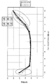
- Figure 5 shows the focus curve based on the average value of each area. Although a minimum point appears on the right side of the focus curve, a minimum point does not appear on the left side of the focus curve, and the signal intensity (average luminance) is greatly reduced. According to the inventor's knowledge, this is because the average luminance of the area where the pattern collapse has occurred is extremely low, and there is an inflection point corresponding to the minimum point that should appear originally when taking the average with the average luminance of other areas. It can be considered that it does not appear, and there is a possibility that pattern collapse has occurred.
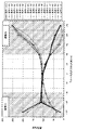
- the focus curves shown in FIGS. 6 to 8 are different from the case of FIG. 5 and have different diffraction conditions.
- the focus curve of the first diffraction condition shown in FIG. 6 when the focus offset is ⁇ 90 nm, the average luminance in the first setting area A1 among the first to sixth setting areas A1 to A6 is larger than the others. It can be seen that pattern collapse has occurred in the first setting area A1.
- the focus offset greatly deviating from “ALL” in FIG. 8 is obtained outside the boundary of the focus offset allowable range.
- the out-of-boundary value (focus offset) obtained by the evaluation unit 43 is ⁇ 90 nm on the minus side.
- the out-of-boundary value obtained by the evaluation unit 43 is ⁇ 90 nm on the minus side and +90 nm on the plus side.
- the out-of-boundary value obtained by the evaluation unit 43 is ⁇ 120 nm on the minus side and +90 nm on the plus side.
- the evaluation unit 43 obtains the allowable range of the focus offset of the exposure apparatus 101 from the previously obtained boundary value (focus offset) (step ST106). At this time, the evaluation unit 43 obtains a range where pattern collapse does not occur in any of a plurality of diffraction conditions.
- FIG. 9 shows the focus curves of FIGS. 6 to 8 superimposed on each other.
- the allowable range of the focus offset obtained by the evaluation unit 43 is ⁇ 60 nm to +60 nm.
- the allowable range is determined to be ⁇ 60 nm to +60 nm.
- the evaluation unit 43 obtains the center position (focus offset amount) of the allowable focus offset range obtained previously as the best focus of the exposure apparatus 101 (step ST107).
- the focus offset of 0 nm located at the center of the allowable range of focus offset of ⁇ 60 nm to +60 nm is the best focus.
- Data relating to the best focus of the exposure apparatus 101 obtained by the evaluation unit 43 is output from the main control unit 45 to the exposure apparatus 101 via the output unit 46 and fed back to the setting of the exposure apparatus 101.
- the line width change amount with respect to the focus change is small with respect to the line width, the best focus can be obtained from the viewpoint of pattern collapse rather than the line width reference.
- the dose for changing the dose amount in the best focus state to obtain the optimum line width is obtained as the best dose.
- the line width can be managed by obtaining the best dose as the line width management.
- the allowable range of the focus offset of the exposure apparatus 101 is obtained based on the image signals (detection signals) of the evaluation wafers 10a to 10j, and based on the allowable range of the focus offset,
- the best focus (the optimum relative position between the wafer and the projection optical system) of the exposure apparatus 101 is obtained. Therefore, the best focus of the exposure apparatus 101 can be obtained in a short time.
- the middle (center) focus position within the focus allowable range as the best focus position, it is possible to accurately obtain the best focus position for a pattern that is difficult to deform even if the focus changes to some extent.
- the best focus position with respect to the ⁇ side allowable range and the + side allowable range is known using SEM or the like, the best focus can be obtained based on the information.
- the negative side allowable range is ⁇ 30 nm and the positive side allowable range is +60 nm.
- the best focus position obtained from the SEM is 2: 1 within the allowable range from the negative side allowable range to the positive side allowable range (the allowable range from the best focus to the negative side is 2 with respect to the positive allowable range from the best focus to the positive side. It is assumed that the range is a point that is internally divided into 1). In this case, the focus offset +30 nm is the best focus.
- the logic IC when the line widths of a plurality of types of patterns are measured with an SEM (scanning electron microscope) or the like, a lot of time is required. However, according to this embodiment, the diffraction conditions are changed for evaluation. Since the diffracted light patterns of the wafers 10a to 10j may be captured and calculated, the allowable range of focus and the best focus position of the exposure apparatus 101 can be obtained in a short time.
- the in-wafer averaging process is performed, but the distribution in the wafer surface can be obtained without averaging.
- the distribution may indicate an autofocus control error of the exposure apparatus.
- a drive error in the Z direction may occur between the forward scan and the reverse scan.
- a shot exposed in the forward scan forward shot
- a shot exposed in the reverse scan reverse shot
- the signal intensity of the corresponding pixels is averaged (average between shots) for all shots in the forward direction shot.
- the shots are averaged for the reverse shots.
- an evaluation wafer was created in which all shots on the wafer were exposed with the same focus offset, but the dose was changed for each vertical step and the focus offset was changed for each horizontal column.
- the best focus can be obtained by using one wafer (so-called FEM wafer).
- FEM wafer a procedure for obtaining the best focus using the FEM wafer will be described.
- the FEM wafer is exposed under the exposure conditions and developed.
- a diffracted light pattern is acquired using a FEM wafer under a plurality of diffraction conditions. Intra-area averaging is performed for each shot of the obtained diffracted light pattern.
- a focus curve is obtained for each diffraction condition, and an allowable focus offset range and a best focus are obtained in the same manner as described above.
- the exposure apparatus 101 is set so that the dose amount is different from the best dose (for example, close to the overdose), and the patterns of the evaluation wafers 10a to 10j are exposed and developed. Also good. In this way, pattern collapse is likely to occur, so that it is possible to increase the detection sensitivity of the tolerance limit (boundary value) of the focus offset.
- the exposure apparatus 101 may be set so that the image surface of the mask pattern is slightly inclined, and the patterns of the evaluation wafers 10a to 10j may be exposed and developed.
- the image plane is tilted so that the right side (X direction + side) with respect to the center of the shot has the same effect as shifting the focus offset to +.
- the focus offset is increased to +, pattern collapse tends to occur on the right side of the shot. Therefore, when the focus offset is swung to +, and the diffraction intensity of the right pattern decreases and the variation of the diffraction intensity in the shot increases, it can be determined that the allowable range of focus offset has been correctly detected.
- the diffraction intensity may have decreased due to factors other than pattern collapse due to defocusing. Judge that range is not required. Since the wrong determination can be eliminated in this way, the reliability of the tolerance limit (boundary value) of the focus offset can be improved.
- the wafer resist film on the wafer
- the wafer may be held in a slightly tilted state. In any case, if the focus state exceeds the allowable range, pattern collapse occurs, and the diffraction reflection intensity at that portion decreases.
- the above-described effects cannot be expected by scanning even if the image plane is tilted in the scanning direction. Therefore, the image plane in the direction orthogonal to the scanning direction (generally the longitudinal direction of the slit image) is inclined.
- ten evaluation wafers 10a to 10j are manufactured, but the present invention is not limited to this, and the increment and range of the focus offset can be set as appropriate.
- 19 evaluation wafers may be manufactured with the focus offset being changed in 19 steps from ⁇ 120 nm to +150 nm in increments of 15 nm.
- the increment of the focus offset it is possible to increase the detection sensitivity of the focus tolerance limit (boundary value).
- the repeating layer of the evaluation wafers 10a to 10j has a base layer.
- ultraviolet light for example, 248 nm or 313 nm
- BARC layer absorption wavelength of the antireflection layer
- the positive and negative focus offsets are greatly swung to detect the diffracted light from the base pattern in a state where no diffracted light is generated from the upper layer repeated pattern.
- the influence of the underlayer can be known in advance.
- a pattern is produced with a focus offset within an allowable range, and the diffraction intensity obtained only from the upper layer pattern can be obtained by subtracting the influence of the base previously obtained from the obtained diffraction intensity.
- the repetitive pattern 12 is not limited to the line pattern as shown in FIG. 3, but may be a hole pattern.
- the wafer orientation angle and A focus curve may be obtained under a plurality of polarization conditions determined by the illumination wavelength or the like, and an allowable range of focus of the exposure apparatus 101 may be obtained from these focus curves.
- the detection conditions increase as compared with the case of only the diffracted light pattern, so that the allowable focus range and the best focus position of the exposure apparatus 101 can be obtained with high accuracy.
- the data related to the best focus obtained by the evaluation unit 43 can be output to the exposure apparatus 101 via the output unit 46 by the main control unit 45 and fed back to the setting of the exposure apparatus 101. it can.
- An exposure system including the surface inspection apparatus 1 according to the above-described embodiment will be described with reference to FIG.
- the exposure system 100 includes an exposure apparatus 101 and the surface inspection apparatus 1 described above.
- the exposure apparatus 101 exposes the resist on the wafer 10 by projecting an image of a predetermined mask pattern (repeated pattern) onto the surface of the wafer 10 coated with the resist.
- the surface inspection apparatus 1 inspects the wafer 10 having the pattern 12 repeatedly formed on the surface through the exposure process by the exposure apparatus 101 and the development process by the developing apparatus (not shown).
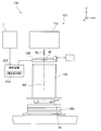
- the exposure apparatus 101 includes an illumination optical system 110 that illuminates the mask M with light EL, a mask stage 120 that can move while holding the mask M, and a pattern of the mask M that is illuminated with light EL.
- the surface inspection apparatus 1 When the above exposure process by the exposure apparatus 101 is performed, the surface inspection apparatus 1 according to the above-described embodiment has the repeated pattern 12 formed on the surface after the development process or the like by the development apparatus (not shown).
- the wafer 10 is inspected. Further, the surface inspection apparatus 1 obtains the best focus of the exposure apparatus 101 as described above at the time of maintenance inspection or every time the wafer 10 of a predetermined lot is exposed, and the exposure apparatus 101 obtains the data related to the obtained best focus. Output to.
- the correction processing unit 210 provided in the control device 200 of the exposure apparatus 101 is based on the data related to the best focus input from the surface inspection apparatus 1, and the focus state at the time of exposure on the surface of the wafer 10 becomes the best focus. As described above, various setting parameters relating to the focus of the exposure apparatus 101 and the arrangement state of the optical elements are corrected.
- the focus of the exposure apparatus 101 is determined based on the data related to the best focus (the optimum relative position between the wafer 10 and the projection optical system 130) output from the surface inspection apparatus 1. Since the setting is adjusted, the adjustment based on the best focus measured accurately in a short time can be performed, and the focus setting of the exposure apparatus 101 can be performed more appropriately.
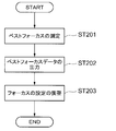
- a flow for obtaining the best focus by the surface inspection apparatus 1 and feeding back to the exposure apparatus 101 will be described with reference to FIG.
- the best focus of the exposure apparatus 101 is obtained as described above using the surface inspection apparatus 1 at the time of maintenance inspection or whenever exposure of the wafer 10 of a predetermined lot is performed (step ST201).
- the data relating to the best focus obtained by the surface inspection apparatus 1 is output to the exposure apparatus 101 (step ST202).
- the focus setting of the exposure apparatus 101 is adjusted based on the data relating to the best focus output from the surface inspection apparatus 1 (step ST203).
- a semiconductor device includes a design process (step ST301) for designing the function and performance of the device, a mask manufacturing process for manufacturing a mask based on the design process (step ST302), and a wafer for manufacturing a wafer from a silicon material.
- a manufacturing process (step ST303), a lithography process (step ST304) for transferring a mask pattern to the wafer by exposure or the like (including an exposure process, a development process, etc.), and a device assembly (dicing process, bonding process, package process, etc.)
- an assembly process (step ST305), an inspection process (step ST306) for inspecting a device, and the like.
- a wafer is prepared (step ST401), and a resist is applied to the wafer surface to have a predetermined thickness using a coating apparatus such as a spin coater (not shown) (step ST402).
- a coating apparatus such as a spin coater (not shown)
- the solvent component of the resist is evaporated by a drying device in the coating device, and film formation is performed on the coated wafer.
- the wafer on which the resist is formed is transferred to the exposure apparatus 101 by a transfer apparatus (not shown) (step ST403).
- the wafer carried into exposure apparatus 101 is aligned by an alignment apparatus provided in exposure apparatus 101 (step ST404).
- the mask pattern is subjected to reduced exposure on the aligned wafer (step ST405).
- the exposed wafer is transferred from the exposure apparatus 101 to a developing device (not shown) and developed (step ST406).
- the developed wafer is set by the surface inspection apparatus 1, and the wafer is inspected as described above (step ST407).
- a wafer in which a defect (abnormality) occurs more than a reference predetermined in the inspection is sent to rework (regeneration processing), and a wafer whose defect (abnormality) is less than the reference is subjected to post-processing such as etching.
- the best focus of the exposure apparatus 101 is required by the surface inspection apparatus 1 at the time of maintenance inspection or whenever exposure of the wafer 10 of a predetermined lot is performed.
- Data related to the best focus obtained by the surface inspection apparatus 1 is output to the exposure apparatus 101, and the focus setting of the exposure apparatus 101 is adjusted (step ST408).
- pattern exposure is performed using the exposure apparatus 101 according to the above-described embodiment in a lithography process.
- the focus setting of the exposure apparatus 101 is adjusted based on the data related to the best focus obtained by the surface inspection apparatus 1 at the time of maintenance inspection or whenever exposure of the wafer 10 of a predetermined lot is performed.
- the pattern is exposed by the exposure apparatus whose focus state is adjusted.
- the best focus the optimum relative position between the wafer 10 and the projection optical system 130
- the focus of 101 can be set more appropriately, and a highly integrated device can be manufactured with high productivity. Further, in the manufacturing method of the present embodiment, since exposure is performed with a good focus state, a highly reliable semiconductor device can be obtained.
- the device manufacturing method of the present embodiment uses a material other than a semiconductor such as a magnetic disk in addition to a device using a semiconductor material. It can also be applied to the production of used devices. Note that the requirements of the above-described embodiments can be combined as appropriate. Some components may not be used. In addition, as long as permitted by law, the disclosure of all published publications and US patents related to the evaluation devices and the like cited in the above embodiments and modifications are incorporated herein by reference.
Landscapes
- Physics & Mathematics (AREA)
- General Physics & Mathematics (AREA)
- Exposure And Positioning Against Photoresist Photosensitive Materials (AREA)
- Exposure Of Semiconductors, Excluding Electron Or Ion Beam Exposure (AREA)
- Length Measuring Devices By Optical Means (AREA)
Abstract
露光装置のベストフォーカス位置を短時間で求めることが可能な装置を提供する。 表面検査装置1は、露光により設けられたパターンを有するウェハの表面を照明する照明系20と、照明系20により照明されたパターンからの回折光による回折光パターンを撮像する撮像装置35と、撮像装置35により撮像された回折光パターンの画像信号に基づいて、露光装置101のフォーカスの許容範囲を求め、求めたフォーカスの許容範囲に基づいて、露光装置101のベストフォーカス位置を求める評価部43とを備えている。
Description
本発明は、露光装置の合焦状態を求める装置および方法に関する。また、この方法を用いたデバイス製造方法に関する。
半導体製造工程で用いられる露光装置は、マスクパターンおよび投影レンズ(投影光学系)を介してレチクルに設けられたマスクパターンを縮小投影することにより、半導体ウェハに対して1ショット分の露光を行うようになっている。
このような露光装置においては、フォーカス(ウェハ面若しくはレジスト表面と投影光学系の焦点面の位置関係)の管理が非常に重要である。露光装置ではフォーカスの制御として幾つかの手法があるが、ここでは投影光学系を固定して、パターンの投影対象である基板(基板上のレジスト表面)を投影光学系の光軸方向に移動(投影光学系と基板との相対位置関係を変更)する方法を対象とする。この光軸方向の移動量はフォーカスオフセットと呼ばれ、最も良好な合焦状態を得られるフォーカスオフセットはベストフォーカスと呼ばれる。ベストフォーカスを計測する方法として、種々の方法を採用することができる。例えば、フォーカスオフセットを変化させて露光・現像したパターンの線幅をSEM(走査型電子顕微鏡)により測定し、フォーカスオフセットの変化に対する線幅の変化が最も小さくなるフォーカスオフセットをベストフォーカスとして求める方法がある。また、別の方法として専用のパターンを用いた投影により基板上にレジストパターンを作製し、パターンを計測することによりベストフォーカスを求める方法もある。
しかしながら、SEMによりベストフォーカスを求めるのには長時間を要している。
本発明は、このような問題に鑑みてなされたものであり、露光装置のベストフォーカスを短時間で求めることが可能な装置および方法を提供することを目的とする。また、この方法を用いたデバイス製造方法を提供することを目的とする。
このような目的達成のため、本発明に係る評価装置は、投影光学系を介して該投影光学系の焦点位置との相対位置を変えた複数回の投影によりそれぞれ設けられたパターンを表面に有する基板を照明する照明部と、前記表面で反射した照明光を検出する検出部と、1回の前記投影範囲内で検出される検出結果のバラツキ量が、所定の条件を超える前記相対位置に基づいて、前記基板と前記投影光学系との最適相対位置を求める演算部とを備える。
また、本発明に係る評価方法は、投影光学系を介して該投影光学系の焦点位置との相対位置を変えた複数回の投影によりそれぞれ設けられたパターンを表面に有する基板を照明し、前記表面で反射した照明光を検出し、1回の前記投影範囲内で検出される検出結果のバラツキ量が、所定の条件を超える前記相対位置に基づいて、前記基板と前記投影光学系との最適相対位置を求める。
また、本発明に係るデバイス製造方法は、投影光学系を用いて基板の表面にパターンを露光するリソグラフィー工程を有したデバイスの製造方法であって、本発明に係る評価方法を用いて、前記基板と前記投影光学系との最適相対位置を求め、該最適相対位置に基づいて前記基板と前記投影光学系を調整し、該調整された状態で前記基板の表面にパターンを露光する。
本発明によれば、露光装置のベストフォーカスを短時間で求めることができる。
以下、図面を参照して本発明の実施形態について説明する。本願に係る評価装置の一例として表面検査装置を図1に示す。本実施形態の表面検査装置1は、半導体ウェハ10(以下、ウェハ10と称する)を支持するステージ5と、照明系20と、受光系30と、撮像装置35と、画像処理部40と、記憶部41と、検査部42と、評価部43と、ハードウェア制御部44および主制御部45とを備えている。
ステージ5は、ウェハ10の回転対称軸(ステージ5の中心軸)を中心に、不図示の回転機構がウェハ10を回転可能に支持する。この回転対称軸を中心とした円を考えた時に、中心から円周上の点に向かう線分と円周上の基準点と中心を結ぶ線分とのなす角を方位角と呼ぶ。ウェハの場合、外周部に設けられたノッチの切り欠き中心位置やオリエンテーションフラットの中心位置を基準として方位角が規定され、ウェハ方位角度と称される。ウェハ10は、不図示の搬送装置により外部から搬送されてステージ5上に載置され、真空吸着によってステージ5上に固定保持される。また、ステージ5は、不図示の傾動機構により、ウェハ10を支持する支持面と平行でウェハ表面を通る軸Tcを中心に図1に双矢印に示されるように、ウェハ10とともに傾動可能に構成されており、照明光の入射角を調整できるようになっている。
照明系20は、照明光を射出する照明ユニット21と、照明ユニット21から射出された照明光をウェハ10の表面に向けて反射させる照明側凹面鏡25とを有し、ステージ5に支持されたウェハ10の表面全面に照明光として平行光を照射する。照明ユニット21は、光源部22と、調光部23と、導光ファイバ24とを有して構成される。光源部22には、メタルハライドランプや水銀ランプ等が用いられる。調光部23は、バンドパスフィルタやNDフィルタを備えており、光源部22からの光のうち所定の波長を有する光の選択と強度調節を行う。導光ファイバ24は、調光部23からの光を照明光として照明側凹面鏡25へ導く。導光ファイバ24の射出部が照明側凹面鏡25の焦点面に配置されており、照明光は照明側凹面鏡25で反射されることより平行光束となってステージ5に支持されたウェハ10の表面に照射される。なお、ウェハ10に対する照明光の入射角と射出角との関係は、ステージ5を傾動させてウェハ10の載置角度を変化させることにより調整可能である。
また、導光ファイバ24と照明側凹面鏡25との間には、照明側偏光フィルタ26が光路上へ挿抜可能に設けられる。図1の実線で示すように、照明側偏光フィルタ26を光路上から抜去した状態で回折光を利用した検査(以下、便宜的に回折検査と称する)が行われる。一方、図1の破線で示すように、照明側偏光フィルタ26を光路上に挿入した状態で偏光(構造性複屈折による偏光状態の変化)を利用した検査(以下、便宜的にPER検査と称する)が行われる(照明側偏光フィルタ26の詳細については後述する)。
受光系30は、ステージ5に対向して配設された受光側凹面鏡31を有し、照明光の照射を受けたときのウェハ10の全面からの射出光(反射光や回折光等)を集光する。受光側凹面鏡31により集光された射出光は、不図示の撮像光学系により撮像装置35の撮像面上に達し、ウェハ10の像が結像される。
また、受光側凹面鏡31と撮像装置35との間には、受光側偏光フィルタ32が光路上へ挿抜可能に設けられる。図1の実線で示すように、受光側偏光フィルタ32を光路上から抜去した状態で回折検査が行われる。一方、図1の破線で示すように、受光側偏光フィルタ32を光路上に挿入した状態でPER検査が行われる(受光側偏光フィルタ32の詳細については後述する)。
撮像装置35は、撮像面上に形成されたウェハ10の像を光電変換して生画像信号を生成し、主制御部45に送る。主制御部45は、撮像装置35から送られた生画像信号を受け、画像処理部40に送る。なお、主制御部45が一旦生画像信号を撮像装置35から受け取った後、画像処理部40に送るように構成されていてもよいが、主制御部45からの指令に基づき、撮像装置35が直接、画像処理部40に生画像信号を送るように構成されていてもよい。以下の説明においても同様である。画像処理部40は、撮像装置35から送られた生画像信号に基づいて、ウェハ10のデジタル画像を生成する。ウェハ10のデジタル画像は、主制御部45により画像処理部40から検査部42および評価部43に送られる。記憶部41には、良品ウェハのデジタル画像が予め記憶されており、検査部42は、ウェハ10のデジタル画像と良品ウェハのデジタル画像とを受け取り比較して、ウェハ10の表面における欠陥(異常)の有無を検査する。検査部42による検査結果およびそのときのウェハ10のデジタル画像は、主制御部45により不図示の画像表示装置で出力表示される。
なお、検査部42によるウェハ10の検査結果およびデジタル画像は、主制御部45により記憶部41に送られて記憶してもよい。また、検査結果およびデジタル画像は、主制御部45により出力部46から外部(例えば、半導体製造ラインの管理システムや露光装置等)へ出力することも可能である。評価部43は、ウェハのデジタル画像を利用して、露光装置101のフォーカスオフセットの許容範囲(デフォーカスによりパターンの倒れやショートなどの欠陥が発生しない範囲)と、露光装置101のベストフォーカス(露光装置の投影光学系とウェハ10との最適相対位置)を求める(詳細は後述する)。なお、主制御部45、評価部43、検査部42、記憶部41、画像処理部40のそれぞれは、装置内に配置することもできるが、有線/無線の通信手段によって互いに通信可能に構成されていれば装置とは独立に配置することもできる。例えば、主制御部45、評価部43、検査部42、記憶部41、画像処理部40の少なくとも1つを中央監視室に配置し工場内LANで通信することもできる。
主制御部45は、ハードウェア制御部44を介して、照明ユニット21やステージ5の作動を制御する。ハードウェア制御部44は、照明ユニット21の光源部22と調光部23を制御し、照明光の波長および強度を調節する。また、ハードウェア制御部44は、ステージ5の回転機構部(図示せず)を制御し、ウェハ方位角度を調整する。また、ハードウェア制御部44は、ステージ5の傾動機構(図示せず)を制御し、照明光の入射角および射出角を調整する。
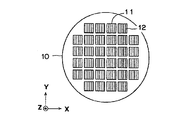
ウェハ10の最上層にはレジスト膜が設けられており、露光装置101により所定のマスクパターンが投影光学系を介して投影露光され、現像装置(図示せず)によって現像される。現像後のウェハ10は、前述のように、不図示の搬送装置により、不図示のウェハカセットまたは現像装置からステージ5上に搬送される。なおこのとき、ウェハ10は、ウェハ10のパターンもしくは外縁部の基準マーク(ノッチやオリエンテーションフラット等)が検出される。ステージ5上に搬送されたウェハ10は、搬送中に検出されたパターンもしくは基準マークの位置に基づいてステージ5の回転機構によりウェハ10のアライメントが行われる。ウェハ10の表面には、図2に示すように、複数のチップ領域(1つの半導体デバイスの製品を構成する範囲)11が縦横に(図2におけるXY方向に)配列される。各チップ領域11の中には、半導体パターンとしてラインパターンまたはホールパターン等の繰り返しパターン12が形成されている。露光の1ショット(マスクパターン1枚分の露光)には、複数のチップ領域が含まれることが多いが、図2では分かりやすさのために、1チップ分の領域を1ショット分の領域としている。
また、露光装置101は、例えばステップ・アンド・スキャン方式の露光装置であり、ケーブル等を介して本実施形態の表面検査装置1の出力部46と電気的に接続され、表面検査装置1からのデータ(信号)に基づいて露光制御の調整を可能となっている。なお、露光装置101と表面検査装置1の出力部46とは、必ずしも電気的に接続されていなくてもよく、有線/無線の通信手段によって通信可能に構成されていてもよい。
以上のように構成される表面検査装置1を用いて、ウェハ10表面の回折検査を行うには、まず、図1に示すように照明側偏光フィルタ26および受光側偏光フィルタ32を光路上から抜去し、ウェハ10をステージ5上に搬送する。
次に、基準マークの検出結果に基づき、ステージ5の回転機構により所定の位置に所定の方向で載置することによりウェハ10のアライメントが行われる。なお、ウェハ10の方向調整は、搬送途中で行っても良い。このアライメントにより、ウェハ10の表面上における照明光の入射方向とパターンの繰り返し方向とが一致(ラインパターンの場合、ラインに対して直交)する。さらに、パターンのピッチをPとし、ウェハ10の表面に照射する照明光の波長をλとし、照明光の入射角をθ1とし、n次回折光の射出角をθ2としたとき、次の数式1を満足するように傾動の設定を行う。このとき、ハードウェア制御部44により、照明ユニット21の光源部22と調光部23や、ステージ5の傾動機構(図示せず)等が制御される。

次に、照明系20により照明光をウェハ10の表面に照射する。このような条件で照明光をウェハ10の表面に照射する際、照明ユニット21における光源部22からの光は調光部23を通過し、所定の波長(例えば、248nmの波長)を有する所定の強度の照明光に調整される。調整された照明光が導光ファイバ24から照明側凹面鏡25へ射出され、照明側凹面鏡25で反射した照明光が平行光束となってウェハ10の表面に照射される。ウェハ10表面の繰り返しパターンで回折した回折光は、受光側凹面鏡31により集光されて撮像装置35の撮像面上に達し、ウェハ10の像(回折光による像)が結像される。以降説明のため、ウェハ方位角度、照明光の波長、傾動角度、回折次数などの組み合わせで決まる回折光の条件を回折条件と称する。なお、上記実施例で不図示の傾動機構によりウェハ10を傾動させたが、ウェハ10を固定して照明系20の照明光の入射角と受光系30の受光角を変更して上記回折条件を満たすようにしても良い。
なお、ウェハ10の回折光パターン(ウェハ10の回折光が撮像面で光の強度信号として得られる画)が図示しない画像表示装置で出力表示される。
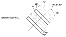
次に、表面検査装置1によりウェハ10表面のPER検査を行う場合について説明する。なお、PER検査で検査する繰り返しパターン12は、図3に示すように、複数のライン部2Aがその短手方向(X方向(図2参照))に沿って一定のピッチPで配列されたレジストパターン(ラインパターン)であるものとする。また、隣り合うライン部2A同士の間は、スペース部2Bである。また、ライン部2Aの配列方向(X方向)を「繰り返しパターン12の繰り返し方向」と称することにする。
PER検査は、繰り返しパターン12におけるライン部2Aとスペース部2Bとの体積比の変化に伴う構造性複屈折の変化を利用して、繰り返しパターン12の異常検査を行うものである。なお、説明を簡単にするため、ライン部2Aとスペース部2Bとの理想的な体積比(設計値)を1:1とする。なお、体積比を断面形状の面積比と言い換えることもできる。
PER検査では、図1の破線で示すように、照明側偏光フィルタ26および受光側偏光フィルタ32が光路上に挿入される。なお、偏光フィルタは1方向の偏光成分を有する光を透過させるフィルタであり、透過できる方向を透過軸と呼ぶ。照明側偏光フィルタ26は、導光ファイバ24と照明側凹面鏡25との間に配設されるとともに、その透過軸が所定の方位(例えば、p偏光が得られる方位)に設定される。
受光側偏光フィルタ32は、受光側凹面鏡31と撮像装置35との間に配設され、その透過軸の方位は、上述した照明側偏光フィルタ26の透過軸に対して直交するように設定される(クロスニコルの状態)。したがって、受光側偏光フィルタ32により、ウェハ10(繰り返しパターン12)からの正反射光のうち直線偏光Lと振動方向が略直角な偏光成分(例えば、s偏光の成分)を通過させて、撮像装置35に導くことができる。なお、受光側偏光フィルタ32を光軸中心に回動可能とし、透過軸の角度を調整することで、感度を向上させることができる。
表面検査装置1によりウェハ10表面のPER検査を行うには、回折検査と同様に搬送の途中で基準マークが検出され、ウェハ10をステージ5上の所定の位置に所定の方向で載置することができる。
次に、図3に示すように、繰り返しパターン12の繰り返し方向がウェハ10の表面における照明光(直線偏光L)の振動方向に対して45度だけ斜めになるように、ステージ5を回転させる。さらに、照明光が照射されたウェハ10からの正反射光を受光系30で受光できる傾動角度に、ステージ5を傾動させる。
次に、照明系20により照明光をウェハ10の表面に照射する。照明光は直線偏光Lとなり、ウェハ10の表面全体に照射される。このとき、直線偏光Lは平行光束なので、ウェハ10の各点における直線偏光Lの入射角度は互いに同じとなる。
PER検査では、繰り返しパターン12の構造性複屈折により直線偏光Lの偏光状態が変化し、正反射光のうち直線偏光Lと振動方向が略直角な偏光成分を通過させて、直線偏光Lと振動方向が略直角な偏光成分によるウェハ10の反射像が撮像素子により撮像される。撮像されたウェハ10の偏光画像は外部に出力されると共に、図示しない画像表示装置で出力表示される。
なお、信号強度とは、撮像装置35の撮像素子で検出される光の強度に応じた信号強度であり、照明光強度、パターンによる回折効率、撮像装置の感度などにより決まるものである。本実施形態においては、信号強度は画像輝度として観測されるので、この2つの言葉は実質的に同じものを指す。
また、上述した回折検査およびPER検査に限らず、ウェハ10表面からの正反射光に基づく検査(以下、便宜的に正反射検査と称する)を行うことも可能である。
ここで、フォーカスオフセットの許容範囲およびベストフォーカスを求める原理を説明する。パターン倒れ(例えば、繰り返しパターン12におけるライン部2Aの倒れ)や、パターンショート(例えば、繰り返しパターン12におけるライン部2A同士の接触)が発生しない場合、ショット内で回折光の強度はほぼ一定である。これに対して、本願の発明者は、パターン倒れ又はパターンショート(以下パターン倒れとパターンショートをまとめてパターン崩れと呼ぶことがある)が発生すると、パターン崩れを起こした部分では回折光の強度が極端に低下する(バラツキが発生)ことを発見した。
本願の発明者の知見によれば、この現象は次のように考えることができる。ベストフォーカスの状態で露光装置によりライン状のマスクパターンが露光され現像されたレジストのパターン形状は、それぞれのパターンのエッジが直角な直方体となっていると考えられる。一方、フォーカスオフセットがベストフォーカスから外れる(デフォーカスになる)と、直方体形状のエッジがだれると共に側面部が波打つようになると考えられている。さらにデフォーカスが大きくなるとパターンが倒れてしまう。パターンが倒れてしまうとその部分では回折光が発生しなくなる(言い換えると、回折光の強度が著しく減少する)。そのため、正常なパターンに合わせた回折条件で回折光パターンを取得すると、デフォーカスでパターンが倒れてしまった部分では回折光が発生しないため信号が無くなる(又は回折光の強度が著しく小さくなるため、信号強度が著しく減少する)。
一方、露光装置の投影光学系の結像面とレジスト面との相対的な傾きを持つ場合を考える。露光範囲の全面がフォーカスオフセット許容範囲に入っていれば、パターン倒れは発生せず全てのパターンから回折光が発生するため、回折光の強度のバラツキは小さい。しかし前述のように結像面とレジスト面との相対的な傾きがあると、1ショット(露光領域)の一部においてフォーカスオフセット許容から外れパターン倒れが発生する。この状態ではフォーカスオフセット許容範囲内の部分では回折光が発生し、フォーカスオフセット許容範囲から外れた部分では回折光が発生せず、1ショット内で回折光の強度のバラツキが大きくなる。
このように、1ショット内での回折光の強度のバラツキからフォーカスの許容範囲を求めることができる。また、フォーカスの許容範囲からベストフォーカスとなるフォーカスオフセットを求めることができる(詳細は後述する)。
次に、上記原理を用いてフォーカスオフセットの許容範囲およびベストフォーカスを求める例を説明する。図4は露光装置101のベストフォーカス(最も良好な合焦状態を得られるフォーカスオフセット)を求める方法を示すフローチャートである。まず、露光装置101のフォーカスオフセット(既知)をウェハごとに変化させて繰り返しパターンを露光し現像した複数のウェハ(例えば、フォーカスオフセット量が0nm,±30nm,±60nm,±90nm,±120nm,+150nmである10枚のウェハ)を作製する(ステップST101)。ここで、便宜上、フォーカスオフセットが異なる10枚のウェハを評価用ウェハ10a~10jと称することにする。
次に、評価用ウェハ10a~10jの回折光パターンをそれぞれ撮像取得する(ステップST102)。このとき、回折検査の場合と同様に、評価用ウェハ10a~10jの回折光パターンを生成する。またこのとき、評価用ウェハ10a~10jについて、露光したマスクパターンの情報または回折条件サーチ(後述)を利用して回折条件を求め、回折光が得られるように回折検査の場合と同様の設定を行う。回折条件サーチとは、正反射以外の角度範囲でステージ5の傾動角度を段階的に変化させてそれぞれの傾動角度で画像を取得し、画像が明るくなる、すなわち回折光が得られる傾動角度を求める機能のことを指す。そして、複数の回折条件における評価用ウェハ10a~10jの回折光パターンをそれぞれ撮像取得する。なお、回折条件サーチは、上述の他、瞳空間での明るさ分布に基づいて傾動角度を求めてもよく、レジスト上のパターンの配置情報をフーリエ変換して回折条件を求めても良い。
次に、画像処理部40は、評価用ウェハ10a~10jの回折光パターンにおいて、各評価用ウェハ10a~10jのそれぞれのウェハ内において全てのショットの対応する部分の画素の信号強度の平均化(以降適宜ウェハ内平均化と称する)を行う(ステップST103)。この平均化により、中央部と外周部によるレジスト膜厚の差や露光装置の光軸方向の駆動制御バラツキによる誤差を低減することができる。なお、信号強度の平均値ではなく最頻値を用いることもできる。また、全てのショットの平均ではなく、回折検査の結果ショット内の欠陥のあるショットについては、除外しても良い。次に、画像処理部40は、ウェハ内平均化によって得られた(すなわち、互いにフォーカスオフセットの異なる)全てのショットについて、図6の右上の囲み部分で示すようにショット内に複数のエリア(小さな長方形で囲んだ領域)A1~A6を設定する。次に、各エリア内で信号強度の平均化(以下、適宜「エリア内平均化」と称する)によって得られた値(以下、適宜「エリア内平均輝度」と称する)をそれぞれ求める。なお、ショット内平均化やエリア内平均化は、評価用ウェハ10a~10jについて回折条件ごとにそれぞれ行われる。ここまでの処理で、複数の回折条件において、フォーカスオフセットを10段階に振ったそれぞれのウェハのエリア内平均輝度が設定領域A1~A6ごとに得られる。
次に、画像処理部40はエリア内平均化されたデータを主制御部45を介して評価部43に送る。評価部43は、図6~図8に示すように、設定領域A1~A6ごとに、エリア内平均輝度とフォーカスオフセットとの関係を示すグラフ(1軸にエリア内平均輝度をもう1軸にフォーカスオフセットをとった2次元グラフ、以下、フォーカスカーブと称する)を求める(ステップST104)。このとき、評価部43は、フォーカスカーブを関数で近似した近似曲線を求めてもよい。なお、この近似曲線の関数には、4次関数(4次式)を用いることができる。また、4次関数は次の数式2のように表される。

ここで、xはフォーカスオフセットであり、yは信号強度(エリア内平均輝度)であり、a,b,c,d,eは係数である。最小二乗法などを用いて、フォーカスカーブを近似するための最適な係数a,b,c,d,eを求めることにより、近似関数が得られる。
次に、評価部43は、複数の回折条件について求めた各フォーカスカーブにおいて、1つ又は複数のエリアのエリア内平均輝度が他のエリアのエリア内平均輝度に対して大きくばらつくフォーカスオフセットを求める(ステップST105)。大きくばらつくとは、あるフォーカスオフセットで各エリア内平均輝度を見たときに、少なくとも1つのエリア内平均輝度が他のエリア内平均値と比較して大きく異なることを示す。ここで、ばらつきの評価の一例として偏差値を用いることができる。例えば、1つのエリア内平均輝度の偏差値が40以下で、他のエリア内平均輝度の偏差値が45以上である場合にばらつくと判定することができる。また、ばらつきの評価の別の一例として、全エリアのエリア内平均輝度の平均値(以下、適宜「エリア間平均値」と称する)と標準偏差σの3倍の値(3σ)を求め、各エリアのエリア内平均輝度とエリア間平均値との差と3σとを比べ、3σを超える差をもつエリアがある場合は大きなバラツキがあると判断することができる。また、ばらつきの評価のさらに別の一例として、上述の近似曲線の関数でフォーカスオフセットに対応する輝度と、そのフォーカスオフセットにおけるエリア内平均輝度を比較して、近似曲線の関数から求まる輝度に対して15%以上小さいエリア内平均輝度がある場合に大きなバラツキがあると判断することもできる。また、他の統計手法によりばらつきが大きいかを判断してもよい。
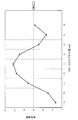
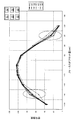
図5に各エリア平均値の平均値によるフォーカスカーブを示す。このフォーカスカーブの右側において極小点が表れているが、フォーカスカーブの左側において極小点が現れずに信号強度(平均輝度)が大きく低下している。発明者の知見によれば、これはパターン崩れを起こしているエリアの平均輝度が極めて低いため他のエリアの平均輝度との平均を取った場合に本来現れるべき極小点に対応する変曲点が現れないものと考えることができ、パターン崩れが発生している可能性がある。
図6~図8に示すフォーカスカーブは、図5の場合と異なるパターンのフォーカスカーブであり、互いに回折条件が異なるものである。図6に示す第1回折条件のフォーカスカーブでは、フォーカスオフセットが-90nmのときに、第1~第6設定領域A1~A6のうち第1設定領域A1のエリア内平均輝度が他に比べて大きく低下しており、第1設定領域A1においてパターン崩れが発生していることがわかる。同様に、図7に示す第2回折条件のフォーカスカーブでは、フォーカスオフセットが-90nmのときに、第1設定領域A1のエリア内平均輝度が他に比べて大きく低下しており,また、フォーカスオフセットが+90nmのときに、第2設定領域A2および第4設定領域A4の信号強度が他に比べて大きく低下している。同様に、図8に示す第3回折条件のフォーカスカーブでは、フォーカスオフセットが-120nmのときに、第5設定領域A5のエリア内平均輝度が他に比べて大きく低下しており,また、フォーカスオフセットが+90nmのときに、第1設定領域A1のエリア内平均輝度が他に比べて大きく低下している。
このように、ショットの一部で信号強度(エリア内平均輝度)が大きく低下するフォーカスオフセット、すなわち、第1~第6設定領域A1~A6のフォーカスカーブのうちいずれかが近似曲線(図5~図8では“ALL”となっている)と大きく乖離するフォーカスオフセットを、フォーカスオフセットの許容範囲の境界外として求める。図6に示す第1回折条件のフォーカスカーブでは、評価部43で求まる境界外値(フォーカスオフセット)がマイナス側で-90nmとなる。図7に示す第2回折条件のフォーカスカーブでは、評価部43で求まる境界外値がマイナス側で-90nm、プラス側で+90nmとなる。図8に示す第3回折条件のフォーカスカーブでは、評価部43で求まる境界外値がマイナス側で-120nm、プラス側で+90nmとなる。このように、回折条件によってフォーカスの許容限界(境界値)が異なることがわかる。
次に、評価部43は、先に求めた境界値(フォーカスオフセット)から露光装置101のフォーカスオフセットの許容範囲を求める(ステップST106)。このとき、評価部43は、複数の回折条件においていずれもパターン崩れが発生しない範囲を求める。ここで、図9は図6~図8のフォーカスカーブをそれぞれ重ねて示したものである。図6~図9の例では、評価部43で求まるフォーカスオフセットの許容範囲が-60nm~+60nmとなる。なお、本実施形態において、図9の領域A、領域Bに示されるように、-90nm以下、及び+90nm以上ではパターン崩れが発生していると考えられるため、許容できない。よって、許容範囲は-60nm~+60nmと求まる。
そして、評価部43は、先に求めたフォーカスオフセットの許容範囲の中央の位置(フォーカスオフセット量)を露光装置101のベストフォーカスとして求める(ステップST107)。図9の例では、-60nm~+60nmのフォーカスオフセットの許容範囲の中央に位置する0nmのフォーカスオフセットがベストフォーカスとなる。評価部43で求められた露光装置101のベストフォーカスに関するデータは、主制御部45から出力部46を介して露光装置101に出力され、露光装置101の設定にフィードバックされる。
近年の微細なパターンにおいては、露光時のフォーカスがベストフォーカスからある程度変化しても、パターンが変形しにくく、あるフォーカス量を超えるとパターン倒れやパターンショートが発生する。線幅に関してもフォーカスの変化に対する線幅変化量が少ないことから、線幅基準ではなく、パターン崩れの観点からベストフォーカスを求めることができる。なおこの場合、初めにベストフォーカスを求めてから、ベストフォーカスの状態でドーズ量を変えて最適な線幅を得るドーズをベストドーズとして求めることになる。このようにして線幅管理としてベストドーズを求めることで、線幅を管理することができる。
このように、本実施形態によれば、評価用ウェハ10a~10jの画像信号(検出信号)に基づいて、露光装置101のフォーカスオフセットの許容範囲を求め、このフォーカスオフセットの許容範囲に基づいて、露光装置101のベストフォーカス(ウェハと投影光学系との最適相対位置)を求める。そのため、露光装置101のベストフォーカスを短時間で求めることができる。
また、フォーカスの許容範囲における中間(中央)のフォーカス位置をベストフォーカス位置として求めることで、フォーカスがある程度変化しても変形しにくいパターンに対するベストフォーカス位置を精度よく求めることができる。なお、SEM等を用いて-側許容範囲と+側許容範囲に対するベストフォーカス位置が分かっていれば、その情報に基づいてベストフォーカスを求めることもできる。例えば、-側許容範囲が-30nmで+側許容範囲が+60nmとする。一方、SEMから得られたベストフォーカス位置が、-側許容範囲から+側許容範囲への許容範囲内を2:1(ベストフォーカスから-側の許容範囲が2に対してベストフォーカスから+側許容範囲が1)に内分する点であることが分かっているとする。この場合、フォーカスオフセット+30nmがベストフォーカスとなる。
また、パターン崩れが発生するとショット内の回折強度のバラツキが大きくなるので、フォーカスカーブを用いてフォーカスオフセットの許容範囲を容易に求めることができる。
なお、ロジックICにおいては、複数種のパターンの線幅をSEM(走査型電子顕微鏡)等で計測すると、多くの時間が必要となるが、本実施形態によれば、回折条件を変えて評価用ウェハ10a~10jの回折光パターンを撮像取得し、演算を行えばよいので、露光装置101のフォーカスの許容範囲およびベストフォーカス位置を短時間で求めることができる。
なお、上述の実施形態では、ウェハ内平均化処理を行ったが、平均化せずにウェハ面内の分布を求めることもできる。この場合、分布は露光装置のオートフォーカスの制御誤差を示すことがある。何らかの理由によりオートフォーカスの結果、ウェハの中央寄りでは投影レンズの結像面がレジスト表面よりも+方向にずれている場合を考える。この場合、上述の方法で求めたベストフォーカスは、ウェハの中央寄りでは周辺に比べて-にずれることからオートフォーカスの制御誤差を知ることができる。
また、スキャン露光でパターンを作製した場合、正方向のスキャンと逆方向のスキャンとでZ方向の駆動誤差が生じる場合がある。このようなスキャン方向によるZ方向の駆動誤差を求めるために、まず正方向のスキャンで露光したショット(正方向ショット)と逆方向のスキャンで露光したショット(逆方向ショット)に分ける。ついで、正方向ショットの全てのショットについて対応する画素の信号強度の平均化(ショット間平均化)を行う。同様に逆方向ショットについてもショット間平均化を行う。得られた正方向ショットのショット間平均化の結果から求めたベストフォーカスと逆方向ショットのショット間平均化の結果から求めたベストフォーカスを比較することで、露光時の正方向のスキャンと逆方向のスキャンそれぞれのフォーカス状態の相違を知ることができる。
また、ウェハ内の全てのショットが同じフォーカスオフセットでパターンの露光を行った評価用ウェハを作製したが、縦方向の段ごとにドーズ量を変化させ、横方向の列ごとにフォーカスオフセットを変化させたウェハ(所謂FEMウェハ)を1枚用いてベストフォーカスを求めることができる。次にFEMウェハを用いてベストフォーカスを求める手順を説明する。まず、前述のように露光条件を振ってFEMウェハを露光し、現像を行う。次いで、FEMウェハを用いて複数の回折条件で回折光パターンを取得する。得られた回折光パターンの各ショットについてエリア内平均化を行う。回折条件ごとにフォーカスカーブを求め、前述と同様にしてフォーカスオフセットの許容範囲およびベストフォーカスを求める。
上述の実施形態において、フォーカスに敏感でフォーカスマージンが少ないクリティカルパターンが経験から分かっている場合は、このクリティカルパターンからの回折光を回路デザインから求め、クリティカルパターンからの回折光に基づいて露光装置101のベストフォーカス位置を求めるようにしてもよい。このようにすれば、より適切なベストフォーカス位置を求めることができる。
上述の実施形態において、ドーズ量がベストドーズと異なるように(例えば、オーバードーズに近い状態に)露光装置101の設定を行って、評価用ウェハ10a~10jのパターンを露光・現像するようにしてもよい。このようにすれば、パターン崩れが発生しやすくなることから、フォーカスオフセットの許容限界(境界値)の検出感度を高めることができる。
上述の実施形態において、マスクパターンの像面が少し傾くように露光装置101の設定を行って、評価用ウェハ10a~10jのパターンを露光・現像するようにしてもよい。例えば、ショット中央に対して右側(X方向+側)を、フォーカスオフセットを+にずらしたのと同様な効果を有するように像面を傾けておく。このようにすれば、フォーカスオフセットを+に振っていくと、まずショット右側でパターン崩れが発生しやすくなる。したがって、フォーカスオフセットを+に振っていき、右側のパターンの回折強度が小さくなりショット内の回折強度のバラツキが大きくなった場合は、正しくフォーカスオフセットの許容範囲が検出できていると判断できる。一方、右側以外ので回折強度が小さくなりショット内の回折強度のバラツキが大きくなった場合は、デフォーカスによるパターン崩れ以外の要因により回折強度が小さくなった可能性があるので、正しくフォーカスオフセットの許容範囲が求められないと判断する。このように間違った判断を排除できることから、フォーカスオフセットの許容限界(境界値)の信頼性を高めることができる。なお、マスクパターンの像面を傾ける代わりに、ウェハ(ウェハ上のレジスト膜)を少し傾けた状態で保持しても良い。いずれの場合も、フォーカス状態が許容範囲を超えればパターン崩れが発生し、その部分の回折反射強度は低下する。
なお、ステップ・アンド・スキャン方式の露光装置の場合は、スキャン方向に像面を傾けてもスキャンにより上記のような効果が期待できない。そのため、スキャン方向と直交する方向(一般にスリット像の長手方向)の像面を傾けることになる。
上述の実施形態において、10枚の評価用ウェハ10a~10jを作製しているが、これに限られるものではなく、フォーカスオフセットの刻みと範囲を適宜設定しうる。例えば、フォーカスオフセットを15nm刻みで-120nm~+150nmの19段階に振った19枚の評価用ウェハを作製するようにしてもよい。このように、フォーカスオフセットの刻みを小さくすることにより、フォーカスの許容限界(境界値)の検出感度を高めることができる。
上述の実施形態において、評価用ウェハ10a~10jの繰り返しパターンに下地層がある場合がある。このような場合は、下地層の上に設けられている反射防止層(BARC層)の吸収波長である紫外光(例えば、248nmや313nm等)を照明光として使用すると、下地パターンからの回折光の影響を低減することができる。このように、下地パターンからの回折光の影響を低減すると、より精度を高くすることができる。
なお、下地パターンからの回折光の影響を全て排除できない場合は、正負のフォーカスオフセットを大きく振り、上層の繰り返しパターンから回折光が発生しない状態で下地パターンからの回折光を検出するようにしてもよい。このように、下地層からの回折強度(信号強度)をモニターすることで、下地の影響を予め知ることができる。次に許容範囲内のフォーカスオフセットでパターンを作製し、得られる回折強度から予め求めた下地の影響を引いて上層のパターンからだけの回折強度を求めることができる。
上述の実施形態において、繰り返しパターン12は、図3に示すようなラインパターンに限らず、ホールパターンであってもよい。
上述の実施形態において、評価用ウェハ10a~10jの回折光パターンに加え、評価用ウェハ10a~10jの偏光画像(PER画像)を利用して、前述の場合と同様の方法により、ウェハ方位角度や照明波長などで決まる複数の偏光条件においてフォーカスカーブを求め、これらのフォーカスカーブから、露光装置101のフォーカスの許容範囲を求めるようにしてもよい。これにより、回折光パターンだけの場合と比べて検出条件が増えるため、露光装置101のフォーカスの許容範囲およびベストフォーカス位置を精度よく求めることができる。
また、上述の表面検査装置1では、評価部43で求めたベストフォーカスに関するデータを、主制御部45により出力部46を介して露光装置101に出力し、露光装置101の設定にフィードバックすることができる。そこで、上述の実施形態に係る表面検査装置1を備えた露光システムについて、図10を参照しながら説明する。この露光システム100は、露光装置101と、上述の表面検査装置1とを備えている。露光装置101は、レジストが塗布されたウェハ10の表面に所定のマスクパターン(繰り返しパターン)の像を投影してウェハ10上のレジストを露光する。表面検査装置1は、前述したように、露光装置101による露光工程および現像装置(図示せず)による現像工程等を経て、表面に繰り返しパターン12が形成されたウェハ10の検査を行う。
露光装置101は、図10に示すように、マスクMを光ELで照明する照明光学系110と、マスクMを保持して移動可能なマスクステージ120と、光ELで照明されたマスクMのパターンの像を所定の縮小倍率でウェハ10に投影する投影光学系130と、ウェハ10を保持して移動可能な基板ステージ150と、露光装置101の各要素及び全体の動作を制御する制御装置200とを備えている。これらの構成により、ウェハ10を保持した基板ステージ150とマスクMを保持したマスクステージ120とを1次元方向に同期移動させて、マスクMのパターンの像をウェハ10に順次投影する動作を繰り返し、ウェハ10の表面に塗布されたレジストを露光していく。
以上の露光装置101による露光工程が実施されると、現像装置(図示せず)による現像工程等を経た後、上述の実施形態に係る表面検査装置1は、表面に繰り返しパターン12が形成されたウェハ10の検査を行う。また、表面検査装置1は、保守点検時や、所定ロットのウェハ10の露光が行われる毎に、前述のようにして露光装置101のベストフォーカスを求め、求めたベストフォーカスに関するデータを露光装置101に出力する。そして、露光装置101の制御装置200に設けられた補正処理部210は、表面検査装置1から入力されたベストフォーカスに関するデータに基づいて、ウェハ10の表面に対する露光時のフォーカス状態がベストフォーカスとなるように、露光装置101のフォーカスに関する各種設定パラメータや光学素子の配置状態を補正する。
これにより、本実施形態の露光システム100によれば、表面検査装置1から出力されたベストフォーカス(ウェハ10と投影光学系130との最適相対位置)に関するデータに基づいて、露光装置101のフォーカスの設定を調整するため、短時間で精度よく計測されたベストフォーカスに基づいた調整が可能となり、露光装置101のフォーカスの設定をより適切に行うことができる。
本実施形態の露光システム100において、表面検査装置1によりベストフォーカスを求めて露光装置101にフィードバックするフローについて、図11を参照しながら説明する。保守点検時や、所定ロットのウェハ10の露光が行われる毎に、表面検査装置1を用いて前述のように露光装置101のベストフォーカスを求める(ステップST201)。次に、表面検査装置1で求めたベストフォーカスに関するデータを、露光装置101に出力する(ステップST202)。そして、表面検査装置1から出力されたベストフォーカスに関するデータに基づいて、露光装置101のフォーカスの設定を調整する(ステップST203)。
続いて、このような露光システム100を用いたデバイス製造方法について説明する。ここでは、一例としてデバイスに半導体材料を使用した半導体デバイスの製造方法について図12を参照しながら説明する。半導体デバイス(図示せず)は、デバイスの機能・性能設計を行う設計工程(ステップST301)、この設計工程に基づいたマスクを製作するマスク製作工程(ステップST302)、シリコン材料からウェハを製作するウェハ製作工程(ステップST303)、露光等によりマスクのパターンをウェハに転写する(露光工程、現像工程等を含む)リソグラフィー工程(ステップST304)、デバイスの組み立てを行う(ダイシング工程、ボンディング工程、パッケージ工程等を含む)組立工程(ステップST305)、デバイスの検査を行う検査工程(ステップST306)等を経て製造される。
ここで、リソグラフィー工程の詳細について、図13を参照しながら説明する。まず、ウェハを用意(ステップST401)し、不図示のスピンコータ等の塗布装置を用いて、ウェハ表面にレジストを所定の厚さとなるように塗布する(ステップST402)。このとき、塗布の終了したウェハに対し、塗布装置内の乾燥装置でレジストの溶剤成分を蒸発させ、成膜を行う。レジストが成膜されたウェハを不図示の搬送装置により露光装置101に搬送する(ステップST403)。露光装置101に搬入されたウェハは、露光装置101に備わっているアライメント装置によりアライメントされる(ステップST404)。アライメントの終了したウェハに、マスクのパターンを縮小露光する(ステップST405)。露光の終了したウェハを露光装置101から不図示の現像装置に移送し、現像を行う(ステップST406)。現像の終了したウェハを表面検査装置1でセットし、前述のようにウェハの検査を行う(ステップST407)。検査で予め決められた基準以上に不良(異常)が発生しているウェハはリワーク(再生処理)に回され、不良(異常)が基準未満のウェハは、エッチング処理等の後処理をされる。なお、保守点検時や、所定ロットのウェハ10の露光が行われる毎に、表面検査装置1により露光装置101のベストフォーカスが求められる。表面検査装置1により求められたベストフォーカスに関するデータは、露光装置101に出力され、露光装置101のフォーカスの設定が調整される(ステップST408)。
本実施形態のデバイス製造方法では、リソグラフィー工程において、前述の実施形態に係る露光装置101を用いてパターンの露光を行う。保守点検時や、所定ロットのウェハ10の露光が行われる毎に、表面検査装置1により求められたベストフォーカスに関するデータに基づいて、露光装置101のフォーカスの設定が調整される。フォーカス設定が調整された後に、フォーカス状態が調整された露光装置によりパターンの露光が行われる。このように、本実施形態のデバイス製造方法によれば、露光装置101のベストフォーカス(ウェハ10と投影光学系130との最適相対位置)を短時間で精度よく計測することができるので、露光装置101のフォーカスの設定をより適切に行うことが可能となり、高集積度のデバイスを生産性良く製造することができる。また、本実施形態の製造方法では、良好なフォーカス状態で露光するため、信頼性の高い半導体デバイスを得ることができる。
なお、本実施形態のデバイス製造方法では、特に半導体デバイスの製造方法について説明したが、本実施形態のデバイス製造方法は、半導体材料を使用したデバイスの他、例えば磁気ディスクなどの半導体以外の材料を使用したデバイスの製造にも適用することができる。
なお、上述の各実施形態の要件は、適宜組み合わせることができる。また、一部の構成要素を用いない場合もある。また、法令で許容される限りにおいて、上述の各実施形態及び変形例で引用した評価装置などに関する全ての公開公報及び米国特許の開示を援用して本文の記載の一部とする。
なお、上述の各実施形態の要件は、適宜組み合わせることができる。また、一部の構成要素を用いない場合もある。また、法令で許容される限りにおいて、上述の各実施形態及び変形例で引用した評価装置などに関する全ての公開公報及び米国特許の開示を援用して本文の記載の一部とする。
1 表面検査装置 5 ステージ
10 ウェハ(10a~10j 評価用ウェハ)
20 照明系(照明部)
30 受光系 35 撮像装置(検出部)
40 画像処理部 41 記憶部
42 検査部 43 評価部(演算部)
44 ハードウェア制御部 45 主制御部
101 露光装置
10 ウェハ(10a~10j 評価用ウェハ)
20 照明系(照明部)
30 受光系 35 撮像装置(検出部)
40 画像処理部 41 記憶部
42 検査部 43 評価部(演算部)
44 ハードウェア制御部 45 主制御部
101 露光装置
Claims (13)
- 投影光学系を介して該投影光学系の焦点位置との相対位置を変えた複数回の投影によりそれぞれ設けられたパターンを表面に有する基板を照明する照明部と、
前記表面で反射した照明光を検出する検出部と、
1回の前記投影範囲内で検出される検出結果のバラツキ量が、所定の条件を超える前記相対位置に基づいて、前記基板と前記投影光学系との最適相対位置を求める演算部とを備える評価装置。 - 前記投影光学系の結像面と前記基板表面とが相対的に傾斜した状態で前記パターンが投影されている請求項1に記載の評価装置。
- 前記照明部が前記基板を照明する照明角と、前記検出部が検出する反射光の反射角度との少なくとも一方を可変する角度調整部をさらに備え、
前記検出部が前記パターンで回折した光を検出する請求項1または2に記載の評価装置。 - 前記照明部が平行光によって前記基板を照明する請求項1から3のいずれか一項に記載の評価装置。
- 前記最適相対位置を外部に出力する出力部をさらに備える請求項1から4のいずれか一項に記載の評価装置。
- 前記照明部は、前記基板を照明する照明光の光路上に挿抜可能に設けられた第1の偏光フィルタを有し、
前記検出部は、前記表面で反射した照明光の光路上に挿抜可能に設けられた第2の偏光フィルタを有する請求項1から5のいずれか一項に記載の評価装置。 - 投影光学系を介して該投影光学系の焦点位置との相対位置を変えた複数回の投影によりそれぞれ設けられたパターンを表面に有する基板を照明し、
前記表面で反射した照明光を検出し、
1回の前記投影範囲内で検出される検出結果のバラツキ量が、所定の条件を超える前記相対位置に基づいて、前記基板と前記投影光学系との最適相対位置を求める評価方法。 - 前記所定の条件が、前記投影光学系の結像面と前記基板表面との相対的な傾斜に対応する請求項7に記載の評価方法。
- 前記パターンで回折した回折光を検出する請求項7または8に記載の評価方法。
- 前記パターンで回折した複数の次数の回折光を検出し、それぞれの次数の回折光の検出結果のバラツキが前記所定の条件を超える前記相対位置を求める請求項9に記載の評価方法。
- 前記所定の条件を超える前記相対位置を、前記最適相対位置を挟む両側で求める請求項7から10のいずれか一項に記載の評価方法。
- 前記両側で求められる相対位置が、お互いに異なる反射条件で検出される検出結果に基づいて求められる請求項11に記載の評価方法。
- 投影光学系を用いて基板の表面にパターンを露光するリソグラフィー工程を有したデバイス製造方法であって、
請求項7から12のいずれか一項に記載の評価方法を用いて、前記基板と前記投影光学系との最適相対位置を求め、
該最適相対位置に基づいて前記基板と前記投影光学系を調整し、
該調整された状態で前記基板の表面にパターンを露光するデバイス製造方法。
Applications Claiming Priority (2)
| Application Number | Priority Date | Filing Date | Title |
|---|---|---|---|
| JP2012037539A JP2015088496A (ja) | 2012-02-23 | 2012-02-23 | 評価装置、評価方法、およびデバイス製造方法 |
| JP2012-037539 | 2012-02-23 |
Publications (1)
| Publication Number | Publication Date |
|---|---|
| WO2013125591A1 true WO2013125591A1 (ja) | 2013-08-29 |
Family
ID=49005773
Family Applications (1)
| Application Number | Title | Priority Date | Filing Date |
|---|---|---|---|
| PCT/JP2013/054202 Ceased WO2013125591A1 (ja) | 2012-02-23 | 2013-02-20 | 評価装置、評価方法、およびデバイス製造方法 |
Country Status (3)
| Country | Link |
|---|---|
| JP (1) | JP2015088496A (ja) |
| TW (1) | TW201342426A (ja) |
| WO (1) | WO2013125591A1 (ja) |
Cited By (2)
| Publication number | Priority date | Publication date | Assignee | Title |
|---|---|---|---|---|
| JP2016151542A (ja) * | 2015-02-19 | 2016-08-22 | アズビル株式会社 | エッジ検出装置 |
| CN120010086A (zh) * | 2025-04-17 | 2025-05-16 | 深圳市永泰光电有限公司 | 光学镜头自动聚焦系统及方法 |
Citations (6)
| Publication number | Priority date | Publication date | Assignee | Title |
|---|---|---|---|---|
| JP2002093697A (ja) * | 2000-07-11 | 2002-03-29 | Tokyo Electron Ltd | 露光条件出し装置と露光条件出し方法および処理装置 |
| JP2002203768A (ja) * | 2000-12-28 | 2002-07-19 | Toshiba Corp | 露光方法、露光システム及び記録媒体 |
| JP2008112889A (ja) * | 2006-10-31 | 2008-05-15 | Matsushita Electric Ind Co Ltd | フォーカス測定方法、半導体装置の製造方法、および露光システム |
| WO2011001678A1 (ja) * | 2009-07-01 | 2011-01-06 | 株式会社ニコン | 露光条件設定方法および表面検査装置 |
| JP2011040433A (ja) * | 2009-08-06 | 2011-02-24 | Nikon Corp | 表面検査装置 |
| JP2011040434A (ja) * | 2009-08-06 | 2011-02-24 | Nikon Corp | 検査装置 |
-
2012
- 2012-02-23 JP JP2012037539A patent/JP2015088496A/ja active Pending
-
2013
- 2013-02-20 WO PCT/JP2013/054202 patent/WO2013125591A1/ja not_active Ceased
- 2013-02-22 TW TW102106162A patent/TW201342426A/zh unknown
Patent Citations (6)
| Publication number | Priority date | Publication date | Assignee | Title |
|---|---|---|---|---|
| JP2002093697A (ja) * | 2000-07-11 | 2002-03-29 | Tokyo Electron Ltd | 露光条件出し装置と露光条件出し方法および処理装置 |
| JP2002203768A (ja) * | 2000-12-28 | 2002-07-19 | Toshiba Corp | 露光方法、露光システム及び記録媒体 |
| JP2008112889A (ja) * | 2006-10-31 | 2008-05-15 | Matsushita Electric Ind Co Ltd | フォーカス測定方法、半導体装置の製造方法、および露光システム |
| WO2011001678A1 (ja) * | 2009-07-01 | 2011-01-06 | 株式会社ニコン | 露光条件設定方法および表面検査装置 |
| JP2011040433A (ja) * | 2009-08-06 | 2011-02-24 | Nikon Corp | 表面検査装置 |
| JP2011040434A (ja) * | 2009-08-06 | 2011-02-24 | Nikon Corp | 検査装置 |
Cited By (2)
| Publication number | Priority date | Publication date | Assignee | Title |
|---|---|---|---|---|
| JP2016151542A (ja) * | 2015-02-19 | 2016-08-22 | アズビル株式会社 | エッジ検出装置 |
| CN120010086A (zh) * | 2025-04-17 | 2025-05-16 | 深圳市永泰光电有限公司 | 光学镜头自动聚焦系统及方法 |
Also Published As
| Publication number | Publication date |
|---|---|
| TW201342426A (zh) | 2013-10-16 |
| JP2015088496A (ja) | 2015-05-07 |
Similar Documents
| Publication | Publication Date | Title |
|---|---|---|
| JP5765345B2 (ja) | 検査装置、検査方法、露光方法、および半導体デバイスの製造方法 | |
| JP5867412B2 (ja) | 表面検査装置及びその方法 | |
| US7697139B2 (en) | Surface inspection apparatus | |
| CN102884609B (zh) | 检查装置及检查方法 | |
| US20140315330A1 (en) | Measurement device, measurement method, and method for manufacturing semiconductor device | |
| US8665430B2 (en) | Exposure condition determining method and surface inspection apparatus | |
| JP5434353B2 (ja) | 表面検査装置および表面検査方法 | |
| JP5434352B2 (ja) | 表面検査装置および表面検査方法 | |
| TW201348888A (zh) | 光學裝置、像差測定方法、及半導體元件之製造方法 | |
| TWI464390B (zh) | Surface inspection device and surface inspection method | |
| JP2015088496A (ja) | 評価装置、評価方法、およびデバイス製造方法 | |
| JP2014215059A (ja) | 評価装置、評価方法、および半導体装置 | |
| JP5994308B2 (ja) | 検査装置、検査方法、およびデバイス製造方法 | |
| JP2004184322A (ja) | 欠陥検査装置および欠陥検査方法 | |
| JPH1022211A (ja) | 位置検出装置及びそれを用いたデバイスの製造方法 | |
| JP2011141137A (ja) | 表面検査装置 |
Legal Events
| Date | Code | Title | Description |
|---|---|---|---|
| 121 | Ep: the epo has been informed by wipo that ep was designated in this application |
Ref document number: 13751615 Country of ref document: EP Kind code of ref document: A1 |
|
| NENP | Non-entry into the national phase |
Ref country code: DE |
|
| 122 | Ep: pct application non-entry in european phase |
Ref document number: 13751615 Country of ref document: EP Kind code of ref document: A1 |