WO2013118686A1 - 表示装置およびその駆動方法 - Google Patents
表示装置およびその駆動方法 Download PDFInfo
- Publication number
- WO2013118686A1 WO2013118686A1 PCT/JP2013/052507 JP2013052507W WO2013118686A1 WO 2013118686 A1 WO2013118686 A1 WO 2013118686A1 JP 2013052507 W JP2013052507 W JP 2013052507W WO 2013118686 A1 WO2013118686 A1 WO 2013118686A1
- Authority
- WO
- WIPO (PCT)
- Prior art keywords
- polarity
- period
- scanning
- frames constituting
- frame
- Prior art date
- Legal status (The legal status is an assumption and is not a legal conclusion. Google has not performed a legal analysis and makes no representation as to the accuracy of the status listed.)
- Ceased
Links
Images


Classifications
-
- G—PHYSICS
- G09—EDUCATION; CRYPTOGRAPHY; DISPLAY; ADVERTISING; SEALS
- G09G—ARRANGEMENTS OR CIRCUITS FOR CONTROL OF INDICATING DEVICES USING STATIC MEANS TO PRESENT VARIABLE INFORMATION
- G09G3/00—Control arrangements or circuits, of interest only in connection with visual indicators other than cathode-ray tubes
- G09G3/20—Control arrangements or circuits, of interest only in connection with visual indicators other than cathode-ray tubes for presentation of an assembly of a number of characters, e.g. a page, by composing the assembly by combination of individual elements arranged in a matrix no fixed position being assigned to or needed to be assigned to the individual characters or partial characters
- G09G3/34—Control arrangements or circuits, of interest only in connection with visual indicators other than cathode-ray tubes for presentation of an assembly of a number of characters, e.g. a page, by composing the assembly by combination of individual elements arranged in a matrix no fixed position being assigned to or needed to be assigned to the individual characters or partial characters by control of light from an independent source
- G09G3/36—Control arrangements or circuits, of interest only in connection with visual indicators other than cathode-ray tubes for presentation of an assembly of a number of characters, e.g. a page, by composing the assembly by combination of individual elements arranged in a matrix no fixed position being assigned to or needed to be assigned to the individual characters or partial characters by control of light from an independent source using liquid crystals
- G09G3/3611—Control of matrices with row and column drivers
- G09G3/3674—Details of drivers for scan electrodes
-
- G—PHYSICS
- G09—EDUCATION; CRYPTOGRAPHY; DISPLAY; ADVERTISING; SEALS
- G09G—ARRANGEMENTS OR CIRCUITS FOR CONTROL OF INDICATING DEVICES USING STATIC MEANS TO PRESENT VARIABLE INFORMATION
- G09G3/00—Control arrangements or circuits, of interest only in connection with visual indicators other than cathode-ray tubes
- G09G3/20—Control arrangements or circuits, of interest only in connection with visual indicators other than cathode-ray tubes for presentation of an assembly of a number of characters, e.g. a page, by composing the assembly by combination of individual elements arranged in a matrix no fixed position being assigned to or needed to be assigned to the individual characters or partial characters
- G09G3/34—Control arrangements or circuits, of interest only in connection with visual indicators other than cathode-ray tubes for presentation of an assembly of a number of characters, e.g. a page, by composing the assembly by combination of individual elements arranged in a matrix no fixed position being assigned to or needed to be assigned to the individual characters or partial characters by control of light from an independent source
- G09G3/3406—Control of illumination source
- G09G3/342—Control of illumination source using several illumination sources separately controlled corresponding to different display panel areas, e.g. along one dimension such as lines
-
- G—PHYSICS
- G09—EDUCATION; CRYPTOGRAPHY; DISPLAY; ADVERTISING; SEALS
- G09G—ARRANGEMENTS OR CIRCUITS FOR CONTROL OF INDICATING DEVICES USING STATIC MEANS TO PRESENT VARIABLE INFORMATION
- G09G3/00—Control arrangements or circuits, of interest only in connection with visual indicators other than cathode-ray tubes
- G09G3/20—Control arrangements or circuits, of interest only in connection with visual indicators other than cathode-ray tubes for presentation of an assembly of a number of characters, e.g. a page, by composing the assembly by combination of individual elements arranged in a matrix no fixed position being assigned to or needed to be assigned to the individual characters or partial characters
- G09G3/34—Control arrangements or circuits, of interest only in connection with visual indicators other than cathode-ray tubes for presentation of an assembly of a number of characters, e.g. a page, by composing the assembly by combination of individual elements arranged in a matrix no fixed position being assigned to or needed to be assigned to the individual characters or partial characters by control of light from an independent source
- G09G3/36—Control arrangements or circuits, of interest only in connection with visual indicators other than cathode-ray tubes for presentation of an assembly of a number of characters, e.g. a page, by composing the assembly by combination of individual elements arranged in a matrix no fixed position being assigned to or needed to be assigned to the individual characters or partial characters by control of light from an independent source using liquid crystals
- G09G3/3611—Control of matrices with row and column drivers
- G09G3/3614—Control of polarity reversal in general
-
- G—PHYSICS
- G09—EDUCATION; CRYPTOGRAPHY; DISPLAY; ADVERTISING; SEALS
- G09G—ARRANGEMENTS OR CIRCUITS FOR CONTROL OF INDICATING DEVICES USING STATIC MEANS TO PRESENT VARIABLE INFORMATION
- G09G2310/00—Command of the display device
- G09G2310/02—Addressing, scanning or driving the display screen or processing steps related thereto
- G09G2310/0264—Details of driving circuits
- G09G2310/0278—Details of driving circuits arranged to drive both scan and data electrodes
-
- G—PHYSICS
- G09—EDUCATION; CRYPTOGRAPHY; DISPLAY; ADVERTISING; SEALS
- G09G—ARRANGEMENTS OR CIRCUITS FOR CONTROL OF INDICATING DEVICES USING STATIC MEANS TO PRESENT VARIABLE INFORMATION
- G09G2310/00—Command of the display device
- G09G2310/02—Addressing, scanning or driving the display screen or processing steps related thereto
- G09G2310/0264—Details of driving circuits
- G09G2310/0283—Arrangement of drivers for different directions of scanning
-
- G—PHYSICS
- G09—EDUCATION; CRYPTOGRAPHY; DISPLAY; ADVERTISING; SEALS
- G09G—ARRANGEMENTS OR CIRCUITS FOR CONTROL OF INDICATING DEVICES USING STATIC MEANS TO PRESENT VARIABLE INFORMATION
- G09G2330/00—Aspects of power supply; Aspects of display protection and defect management
- G09G2330/02—Details of power systems and of start or stop of display operation
- G09G2330/021—Power management, e.g. power saving
- G09G2330/022—Power management, e.g. power saving in absence of operation, e.g. no data being entered during a predetermined time
-
- G—PHYSICS
- G09—EDUCATION; CRYPTOGRAPHY; DISPLAY; ADVERTISING; SEALS
- G09G—ARRANGEMENTS OR CIRCUITS FOR CONTROL OF INDICATING DEVICES USING STATIC MEANS TO PRESENT VARIABLE INFORMATION
- G09G2340/00—Aspects of display data processing
- G09G2340/04—Changes in size, position or resolution of an image
- G09G2340/0407—Resolution change, inclusive of the use of different resolutions for different screen areas
- G09G2340/0435—Change or adaptation of the frame rate of the video stream
Definitions
- the present invention relates to a display device that performs polarity inversion driving and a driving method of the display device.
- liquid crystal display devices are widely installed in various electronic devices. Since the liquid crystal display device has various advantages such as thinness, light weight, and low power consumption, its use is expected to further advance in the future.
- the liquid crystal display device has a problem that the display panel is burned when driven by direct current. Therefore, in order to prevent such burn-in, it is common to drive the liquid crystal display device with polarity inversion.
- polarity inversion driving is performed, the polarity of image data (data signal) written in each pixel constituting the display panel is inverted for each frame.
- the polarity of the voltage applied to the liquid crystal in each pixel is also inverted every frame, so that the polarity of the charge in the liquid crystal is not biased to positive or negative during the operation of the display device. As a result, burn-in of the display panel can be prevented.
- pause driving has been proposed.
- a display device that performs pause driving scans the display panel in a certain frame and then does not scan the display panel in a certain number of consecutive frames. In this rest period, the voltage applied to the pixels of the display panel in the immediately preceding frame is held, and thereby the display is also maintained. Since the signal output process for the display panel is not performed in the idle period, power consumption can be reduced accordingly.
- Patent Publication 2011-48057 (published March 10, 2011)
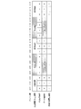
- FIG. 6 is a diagram illustrating the polarity of the liquid crystal applied voltage in each frame when the liquid crystal display device according to the related art executes pause driving.
- the number of frames of the scanning signal is four, while the number of frames in the pause period is four. That is, the sum of the number of frames constituting the scanning period and the number of frames constituting the pause period is an even number. Further, the scanning period and the rest period are alternately repeated.
- the polarity of the data signal is inverted every frame. Therefore, the polarity of the liquid crystal applied voltage is also reversed for each frame.
- the polarities of the liquid crystal applied voltages in the last frame in each scanning period are equal to each other. In the example of FIG. 6, both are positive.
- the liquid crystal applied voltage in the pixels during each pause period is held at the last frame in the scanning period located immediately before the pause period. This is due to the action of the capacitive component present in each pixel.
- the liquid crystal applied voltages in each pause period are equal to each other in any pause period. In the example of FIG. 6, both are negative.
- the charge in the liquid crystal is negatively biased during operation. This becomes more pronounced as the rest period becomes longer.
- the pause drive can be executed, but there are cases where it is inevitable that the screen of the display panel is burned.
- the present invention has been made to solve the above problems, and according to the display device of one embodiment of the present invention, it is possible to perform pause driving and to prevent the display panel from being burned. There is an effect.
- a display device comprising a plurality of scanning lines, a plurality of data lines intersecting with the plurality of scanning lines, and a plurality of pixels individually provided in the vicinity of the intersections of the plurality of scanning lines and the plurality of data lines
- a frame number calculation unit for calculating the number of frames constituting a scanning period for scanning all areas on the screen of the display panel and the number of frames constituting a pause period for not scanning at least a part of the area on the screen.
- a control signal output unit that outputs a control signal that alternately indicates the scanning period and the pause period;
- a polarity indication signal output unit that outputs a polarity indication signal that indicates the polarity of the data signal output to each data line while inverting the polarity of the polarity indication signal for each frame;
- a drive circuit for outputting the data signal having a polarity based on the polarity of the polarity instruction signal input at the time of each frame in each of the scanning periods to each of the data lines;
- the frame number calculation unit calculates the number of frames constituting the scan period and the pause period. The number of frames constituting each is recalculated until the determination value becomes an odd number.
- a method for driving a display device comprising: A frame number calculating step for calculating the number of frames constituting a scanning period for scanning all areas on the screen of the display panel and the number of frames constituting a rest period for not scanning at least a part of the area on the screen.
- Each frame in each scanning period includes a driving step of outputting the data signal having a polarity based on the polarity of the polarity instruction signal input at the time of the frame to each data line,
- a display device comprising a plurality of scanning lines, a plurality of data lines intersecting with the plurality of scanning lines, and a plurality of pixels individually provided in the vicinity of the intersections of the plurality of scanning lines and the plurality of data lines
- a frame number calculation unit for calculating the number of frames constituting a scanning period for scanning all areas on the screen of the display panel and the number of frames constituting a pause period for not scanning at least a part of the area on the screen.
- a determination value calculation unit for calculating a certain determination value;
- a control signal output unit that outputs a control signal that alternately indicates the scanning period and the pause period;
- a polarity instruction signal output unit that outputs a polarity instruction signal that indicates the polarity of the data signal output to each data line while inverting the polarity of the polarity instruction signal for each frame of the polarity inversion period;
- a drive circuit for outputting the data signal having a polarity based on the polarity of the polarity instruction signal input at the time of each frame in each of the scanning periods to each of the data lines;
- a method for driving a display device comprising: A calculation step for calculating the number of frames constituting a scanning period for scanning all areas in the screen of the display panel and the number of frames constituting a pause period for not scanning at least a part of the area on the screen; When the sum of the number of frames constituting the scanning period and the number of frames constituting the pause period is a multiple of the polarity inversion period equal to or greater than 2, the sum is divided by the polarity inversion period.
- a determination value calculation step for calculating a certain determination value;
- a control signal output step for outputting a control signal for alternately instructing the scanning period and the pause period when the determination value is an odd number;
- a polarity instruction signal output step for outputting a polarity instruction signal indicating the polarity of the data signal output to each data line while inverting the polarity of the polarity instruction signal for each frame of the polarity inversion period;
- Each frame in each scanning period includes a driving step of outputting the data signal having a polarity based on the polarity of the polarity instruction signal input at the time of the frame to each data line,
- the display device has an effect of being able to perform pause driving and not causing the display panel to burn.
- FIG. 1 is a block diagram showing details of the configuration of the display system 1 according to the present embodiment.
- the display system 1 includes a display device 2 and a control unit 3.
- the control unit 3 displays and outputs an image via the display device 2.
- the control unit 3 can output arbitrary information such as still images or symbols to the display device 2 in addition to the video.
- the display device 2 includes a display panel 2a, a scanning line driving circuit 4, a data line driving circuit 5 (driving circuit), a common electrode driving circuit 6, and a timing control unit 7 (video signal receiving unit).
- the timing control unit 7 includes a pause drive control unit 8 (control signal output unit, instruction signal reception unit, video signal reception unit, frame number calculation unit, determination value calculation unit) and polarity inversion control unit 9 (polarity instruction signal output unit). It has.
- the display panel 2a includes a screen having a plurality of pixels arranged in a matrix.
- the display panel 2a includes N (N is an arbitrary integer) scanning lines G (gate lines) for selecting and scanning the screen line-sequentially.
- the display panel 2a includes M (M is an arbitrary integer) data lines S (source lines) that supply data signals to pixels for one row included in the selected line.
- the scanning line G and the data line S intersect each other. Each pixel is individually provided in the vicinity of each intersection of the plurality of scanning lines G and the plurality of data lines S.
- the display panel 2a further includes a liquid crystal layer (not shown). That is, the display device 2 is a so-called liquid crystal display device.
- G (n) shown in FIG. 2 represents the nth scanning line G (n is an integer from 1 to N).
- G (1), G (2), and G (3) represent the first, second, and third scanning lines G, respectively.
- S (m) represents the m-th data line S (m is an integer from 1 to M).
- S (1), S (2), and S (3) represent the first, second, and third data lines S, respectively.
- the scanning line driving circuit 4 sequentially scans each scanning line G from the top to the bottom of the screen, for example. At that time, a rectangular wave for turning on a switching element (pixel thin film transistor (TFT)) provided in the pixel and connected to the pixel electrode is output to each scanning line G. Thereby, the pixels for one row in the screen are selected.
- a switching element pixel thin film transistor (TFT)
- the data line driving circuit 5 calculates the value of the voltage to be output to each pixel for the selected row from the video signal (arrow A) input from the control unit 3, and the voltage (data signal) of that value. Is output to each data line S. As a result, image data is supplied to each pixel (pixel electrode) on the selected scanning line G.
- the display device 2 includes a common electrode (not shown) provided for each pixel in the screen.
- the common electrode drive circuit 6 outputs a predetermined common voltage for driving the common electrode to the common electrode based on the signal (arrow B) input from the timing control unit 7 (arrow C).
- the timing control unit 7 outputs a reference signal for each circuit to operate in synchronization with each circuit based on the clock signal, the horizontal synchronization signal, and the vertical synchronization signal input from the control unit 3. .
- the gate start pulse signal GSP, the gate clock signal GCK, and the gate output enable signal GOE are output to the scanning line driving circuit 4 based on the clock signal, the horizontal synchronization signal, and the vertical synchronization signal.
- the data line driving circuit 5 outputs a source start pulse signal SSP, a source latch strobe signal SLS, and a source clock signal SCK based on the clock signal, the horizontal synchronization signal, and the vertical synchronization signal.
- the scanning line driving circuit 4 starts scanning the display panel 2a with the gate start pulse signal GSP received from the timing control unit 7 as a cue, and in accordance with the gate clock signal GCK which is a signal for shifting the selection state of the scanning line G. A selection voltage is sequentially applied to each scanning line G.
- the data line driving circuit 5 Based on the source start pulse signal SSP received from the timing control unit 7, the data line driving circuit 5 stores the input image data of each pixel in a register according to the source clock signal SCK. Then, after storing the image data, the data line driving circuit 5 writes the image data to the pixel electrode through each data line S of the display panel 2a in accordance with the next source latch strobe signal SLS. For example, an analog amplifier included in the data line driving circuit 5 is used for writing the image data.
- the voltage necessary for the operation of each circuit in the display system 1 is supplied from, for example, a power generation circuit (not shown), but this power generation circuit may be included in the control unit 3.
- the power supply voltage Vdd is supplied to the data line driving circuit 5.
- the display device 2 performs so-called pause driving in order to reduce power consumption during operation. Below, the rest drive which the display apparatus 2 performs is demonstrated.
- the control unit 3 instructs the display device 2 to perform pause driving.
- a control signal (instruction signal) indicated by an arrow D is output to the timing control unit 7.
- the pause drive control unit 8 in the timing control unit 7 receives such a control signal from the outside of the display device 2.
- the control signal includes information indicating the number of frames constituting a scanning period for scanning all areas on the screen of the display panel 2a and information indicating the number of frames constituting a pause period during which at least a part of the area is not scanned. It is out.
- the at least part of the area is referred to as a rest area.
- the pause drive control unit 8 calculates the number of frames constituting the scanning period and the number of frames constituting the pause period based on the received control signal. In this case, since the information indicating the number of each frame is included in the control signal, the number of frames indicated by the respective information is directly used as the number of frames constituting the scanning period and the number of frames constituting the pause period. Calculate as a number.
- the pause drive control unit 8 generates a control signal for alternately instructing the scanning period including the calculated number of frames and the pause drive including the calculated number of claims, and outputs the control signal to the scanning line driving circuit 4 and the data line driving circuit 5. (Arrows E and F). At this time, for example, a control signal is output that takes the H value in each frame during the scanning period and takes the L value in each frame during the pause period. As a result, in the display system 1, the pause driving of the display device 2 can be controlled from the outside.
- the scanning line driving circuit 4 and the data line driving circuit 5 specify a scanning period and a pause period based on the received control signal.
- the scanning line driving circuit 4 outputs a scanning signal to each scanning line G in the entire screen of the display panel 2a
- the data line driving circuit 5 outputs a data signal in the entire screen of the display panel 2a. Is output to each data line S.
- the scanning line driving circuit 4 does not output the scanning signal to each scanning line G in the pause area.
- the data line driving circuit 5 may or may not output a data signal to each data line S in the pause region.
- the power consumption necessary for outputting the scanning signal to the pause region can be at least reduced in the pause period, so that the power consumption of the display device 2 in the pause period is much larger than that in the drive period.
- the display device according to one embodiment of the present invention can operate with lower power than a display device that does not perform pause driving.
- it is preferable that no data signal is output to each data line S in the pause area.
- a data signal corresponding to black display may be output to each data line S in the pause region.
- the pause drive is suitable for displaying an image including an area where the content does not change over a certain number of frames.
- the pause drive control unit 8 can calculate the number of frames constituting the scanning period and the number of frames constituting the pause period based on the video signal indicated by the arrow A. In this case, the control signal indicated by the arrow D is not input from the control unit 3 to the timing control unit 7.
- the pause drive control unit 8 analyzes the content of the input video signal, and calculates the number of frames constituting the scanning period and the number of frames constituting the pause period according to the video represented by the video signal. Therefore, if the content of the video represented by the video signal changes, the number of calculated frames also changes. As a result, the pause drive control unit 8 generates control signals that respectively indicate the scanning period and the pause period of the optimum number of frames according to the video signal. As a result, the display device 2 can execute the optimum pause drive according to the video signal.
- the pause drive control unit 8 can calculate the number of frames constituting the scanning period and the number of frames constituting the pause period based on information stored in a memory (storage unit) (not shown). In this case, the control signal indicated by the arrow D is not input from the control unit 3 to the timing control unit 7. Further, the pause drive control unit 8 does not need to analyze the video signal.
- the pause drive control unit 8 reads these pieces of information from the memory, and calculates the number of frames indicated by each piece of information as it is as the number of frames constituting the scanning period and the number of frames constituting the pause period.
- Polarity inversion drive In the display device 2, so-called polarity inversion driving is performed in order to prevent flickering and image sticking during operation.
- the polarity inversion driving will be described below.
- the pause drive control unit 8 in the timing control unit 7 sends a polarity instruction signal (hereinafter referred to as a POL signal) to instruct the polarity of the data signal output to each data line to the data line drive circuit 5.
- a POL signal a polarity instruction signal
- the polarity inversion control unit 9 inverts the polarity for each frame when outputting the POL signal.
- the data line driving circuit 5 outputs, to each data line G, a data signal having a polarity based on the polarity of the POL signal input during the frame in each frame in the scanning period. For example, if the polarity of the POL signal is positive (+), a data signal having the same positive (+) polarity is output to each data line S. On the other hand, if the polarity of the POL signal is negative ( ⁇ ), a data signal having the same negative ( ⁇ ) polarity is output to each data line S.
- the polarity of the POL signal is inverted for each frame, the polarity of the data signal output from the data line driving circuit 5 is similarly inverted for each frame. Therefore, in the display device 2, the polarity of the voltage applied to the liquid crystal is also inverted for each frame in each frame within the scanning period.
- the polarity of the POL signal and the polarity of the data signal output to each data line S do not necessarily match.
- the polarity of the data signal is inverted for each data line S in the same frame. Therefore, in the same frame, when the polarity of the POL signal is positive, the polarity of the data signal output to the data line S (0) is positive, but the polarity of the data signal output to the data signal S (1) is
- the display device 2 can also perform processing that is negative.
- the polarity inversion method (Specific example of polarity reversal method)
- the polarity inversion method will be described in detail with reference to FIGS. 2 and 3.
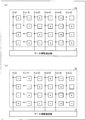
- the polarity inversion method “dot inversion” and the polarity inversion method “source inversion” are performed using a plurality of pixels arranged in 6 pixel columns ⁇ 4 pixel rows, which are some pixels provided in the display panel 2a. "Will be described.
- FIG. 2 is a diagram showing the display panel 2a in a state where the source signal is written by the polarity inversion method “dot inversion”.
- FIG. 3 is a diagram showing the display panel 2a in which a source signal is written by the polarity inversion method “source inversion”.
- a pixel indicated by “+” indicates a state in which positive polarity data is written to the pixel
- a pixel indicated by “ ⁇ ” indicates that the pixel is A state in which the negative electrode data is written is shown.
- the pixel arrangement in each pixel column is “+, ⁇ , +, ⁇ ” in the spatial direction of the display panel (pixel column direction and pixel row direction).
- the polarity of the source signal is inverted for each pixel, such as “ ⁇ , +, ⁇ , +”.
- the pixel arrangement in each pixel column is “+, +, +, +” or “ ⁇ , ⁇ , ⁇ , ⁇ ”. Furthermore, the polarities of the source signals of all the pixels are the same. In addition, the pixel arrangement in each pixel row is such that the polarity of the source signal is inverted for each pixel, such as “+, ⁇ , +, ⁇ ” or “ ⁇ , +, ⁇ , +”.
- FIG. 3 when “source inversion” is adopted as the spatial period of polarity inversion, when “1 frame inversion” is adopted as the temporal period of polarity inversion, the display panel 2 a As shown in “FIG. 3A, FIG. 3B, FIG. 3A, FIG. 3B,...”, The polarity of each pixel is inverted every frame.
- “2-frame inversion” is adopted as the time period of polarity inversion, “FIGS. 3A, 3A, 3B, 3B,...
- the polarity of each pixel is inverted every two frames.
- the display device 2 (Combination of pause drive and polarity inversion drive)
- the display device 2 simultaneously performs pause driving and polarity inversion driving. This point will be described in detail below with reference to FIG.
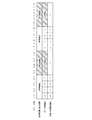
- FIG. 4 is a diagram showing the polarity of the liquid crystal applied voltage in each frame when the display device 2 of the present embodiment performs pause driving.
- the number of frames constituting the scanning signal is 3, while the number of frames constituting the pause period is four. That is, the sum of the number of frames constituting the scanning period and the number of frames constituting the pause period is an odd number.
- the polarity of the POL signal is inverted every frame during either the scanning period or the pause period.
- the polarity of the POL signal in n + 1 frames (n is a natural number) in the scanning period is positive, and the polarity of the POL signal in the next frame n + 2 is negative.
- the polarity of the POL signal in the n + 3 frame is positive. This relationship is maintained in each frame within the pause period. Therefore, the polarity of the POL signal in the n + 4 frame within the pause period is negative, and the polarity of the POL signal in the n + 5 frame is positive.
- a data signal having a polarity corresponding to the polarity of the POL signal is input to each data line S in each frame in each scanning signal.
- a data signal having the same positive polarity is input to the data line S.
- a data signal having the same negative polarity is input to the data line S. Therefore, in each frame, the polarity of the POL signal and the polarity of the data line S coincide with each other.
- the polarity of the data line S in the first frame in each scanning period is Inverts every scanning period.
- the polarity of the data line S in the n + 1 frame that is the first frame in the first scanning period in FIG. 4 is positive
- the polarity of the data line S in the n + 8 frame that is the first frame in the next scanning period is positive
- the polarity of the data line S is positive in the n + 15 frame, which is the first frame in the next scanning period.
- the polarity of the data line S in the last frame in each scanning period is also inverted every scanning period.
- the polarity of the data line S in the n + 3 frame that is the last frame in the first scanning period in FIG. 4 is negative
- the polarity of the data line S in the n + 10 frame that is the last frame in the next scanning period is negative
- the polarity of the data line S in the n + 17 frame, which is the last frame in the next scanning period is positive.
- the liquid crystal applied voltage having the same polarity as the polarity of the data line S in the last frame in the scanning period located immediately before the pause period is maintained in the pixels in each pause period. This is due to the action of the capacitive component present in each pixel. Therefore, in the display device 2 of the present embodiment, the polarity of the liquid crystal applied voltage held in the pixels during each pause period is inverted every pause period. For example, the liquid crystal applied voltage in each frame in the first pause period shown in FIG. 4 is positive, the liquid crystal applied voltage in each frame in the next pause period is negative, and the next pause period. The liquid crystal applied voltage in each frame within the period is positive.
- the polarity of the liquid crystal applied voltage is inverted for each frame in each scanning period.
- the polarity of the liquid crystal applied voltage is also reversed at every rest period. Therefore, even if the display device 2 continues to operate, the polarity of the liquid crystal applied voltage of each pixel is balanced and does not bias to either positive polarity or negative polarity. As a result, there is no bias in the liquid crystal, and the display panel does not burn.
- the control unit 3 when instructing the pause drive, the control unit 3 outputs a control signal in which the sum of the number of frames constituting the scanning period and the number of frames constituting the pause period is an even number to the timing control unit 7. Can also be output.
- This has the same meaning as instructing the display device 2 to drive in the manner shown in FIG.
- the pause drive control unit 8 calculates the number of frames constituting the scanning period and the number of frames constituting the pause period based on the control signal, the sum of the number of frames becomes an even number. Therefore, when the pause drive control unit 8 generates a control signal (arrows E and F) for instructing the scanning period and the pause period based on the calculation result as it is, the display panel 2a is burned in as in the prior art. End up.
- the pause drive control unit 8 when the sum of the calculated number of frames is an even number, the pause drive control unit 8 counts the number of frames constituting the scanning period and the number of frames constituting the pause period. Are recalculated until the sum becomes an odd number. For example, if the number of frames constituting the scanning period is calculated to be 4 while the number of frames constituting the pause period is calculated to be 4, the former is immediately calculated as 3 and the latter as 4. cure. In other words, no matter what control signal is received, the pause drive control unit 8 keeps the sum of the number of frames constituting the scanning period and the number of frames constituting the pause period as an odd number. That is, the instruction to make the sum of the number of frames constituting the scanning period and the number of frames constituting the pause period even is ignored.
- the sum of the number of frames constituting the scanning period and the number of frames constituting the pause period is always fixed to an odd number and never changes to an even number. .
- the state where the polarity of the liquid crystal applied voltage of each pixel is not biased to either positive polarity or negative polarity is always maintained. Therefore, the state where the display panel does not burn-in is always maintained.
- the display device 2 has an advantage that it is possible to perform pause driving and the display panel is not burned.
- a TFT in which a so-called oxide semiconductor is used for a semiconductor layer is employed as each TFT of a plurality of pixels included in the display panel 2a.
- a TFT in which so-called IGZO (InGaZnO x ), which is an oxide composed of indium (In), gallium (Ga), and zinc (Zn), is used for the semiconductor layer is employed.
- IGZO InGaZnO x
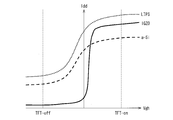
- FIG. 5 is a diagram illustrating characteristics of various TFTs including a TFT using an oxide semiconductor.
- a TFT using an oxide semiconductor a TFT using an oxide semiconductor, a TF using a-Si (amorphous silicon).
- LTPS Low Temperature Poly Silicon
- the horizontal axis (Vgh) indicates the voltage value of the ON voltage supplied to the gate in each TFT
- the vertical axis (Id) indicates the amount of current between the source and drain in each TFT.
- a period indicated as “TFT-on” in the figure indicates a period in which the transistor is on according to the voltage value of the on-voltage
- a period indicated as “TFT-off” in the figure Indicates a period in which it is in an OFF state according to the voltage value of the ON voltage.
- a TFT using an oxide semiconductor has higher electron mobility in the on state than a TFT using a-Si.
- a TFT using a-Si has an Id current of 1 uA when the TFT is turned on, whereas a TFT using an oxide semiconductor is used when the TFT is turned on.
- the Id current is about 20 to 50 uA.
- a TFT using an oxide semiconductor has an electron mobility about 20 to 50 times higher in an on state than a TFT using a-Si, and has an excellent on-characteristic. .
- the display device 2 of the present embodiment employs a TFT using such an oxide semiconductor for each pixel.
- the pixels can be driven by smaller TFTs, and therefore, the proportion of the area occupied by the TFTs in each pixel is reduced. can do. That is, the aperture ratio in each pixel can be increased, and the backlight transmittance can be increased. As a result, a backlight with low power consumption can be adopted or the luminance of the backlight can be suppressed, so that power consumption can be reduced.
- the data signal writing time for each pixel can be further shortened, so that the refresh rate of the display panel 2a can be easily increased.
- a TFT using an oxide semiconductor has less leakage current in an off state than a TFT using a-Si.
- a TFT using a-Si has an Id current of 10 pA at the time of TFT-off, whereas a TFT using an oxide semiconductor is at the time of TFT-off.
- the Id current is about 0.1 pA.
- TFTs using oxide semiconductors have a leakage current in the off state of about 1/100 that of TFTs using a-Si.
- the display device 2 of the present embodiment since the display device 2 of the present embodiment has excellent TFT off characteristics, the state in which the data signals of the plurality of pixels of the display panel 2a are written can be maintained for a long time. In addition, pause driving can be performed while maintaining high display image quality. Also, it is possible to take a longer rest period.
- the polarity inversion period of the POL signal may be at least one frame. That is, the polarity inversion period may be one frame or a plurality of frames.
- the polarity inversion period is one frame, the polarity of the data signal is inverted for each frame in the scanning period. Therefore, the influence of flicker can be further reduced, and as a result, display quality can be further improved.
- the polarity inversion period is a plurality of frames, the polarity inversion frequency of the data signal can be reduced, so that the power consumption of the display device 2 can be further reduced.
- the number of frames constituting the scanning period and the number of frames constituting the pause period must be multiples of the polarity inversion period.
- the pause drive control unit 8 calculates the number of frames constituting the scanning period and the number of frames constituting the pause period, respectively.
- a determination value that is a value obtained by dividing the sum by the polarity inversion period is calculated.
- the determination value is equal to the sum. Therefore, the sum itself can be treated as a determination value.
- the pause drive control unit 8 When the calculated determination value is an odd number, the pause drive control unit 8 generates a control signal for alternately instructing a scanning period consisting of the calculated number of frames and a pause period consisting of the calculated number of frames. On the other hand, when the calculated determination value is an even number, the number of frames constituting the scanning period and the number of frames constituting the pause period are recalculated until the determination value becomes an odd number. With these devices, the display device 2 can always maintain a state in which the polarity of the liquid crystal applied voltage during the rest period is not biased to either positive or negative.
- the pause drive control unit 8 calculates that the number of frames constituting the scanning period is six and the number of frames constituting the pause period is eight.
- the pause drive control unit 8 calculates that the number of frames constituting the scanning period is eight and the number of frames constituting the pause period is eight.
- the pause area on the screen of the display panel 2a is, for example, a half area of the screen or all areas.
- the rest area is all areas on the screen, the output of the scanning signal to all the scanning lines G in the screen is stopped in the rest period. Therefore, the power consumption of the display device 2 can be further reduced.
- a display device includes: A display panel comprising a plurality of scanning lines, a plurality of data lines intersecting with the plurality of scanning lines, and a plurality of pixels individually provided in the vicinity of the intersections of the plurality of scanning lines and the plurality of data lines
- a frame number calculation unit for calculating the number of frames constituting a scanning period for scanning all areas on the screen of the display panel and the number of frames constituting a pause period for not scanning at least a part of the area on the screen.
- a control signal output unit that outputs a control signal that alternately indicates the scanning period and the pause period;
- a polarity indication signal output unit that outputs a polarity indication signal that indicates the polarity of the data signal output to each data line while inverting the polarity of the polarity indication signal for each frame;
- a drive circuit for outputting the data signal having a polarity based on the polarity of the polarity instruction signal input at the time of each frame in each of the scanning periods to each of the data lines;
- the frame number calculation unit calculates the number of frames constituting the scan period and the pause period. The number of frames constituting each is recalculated until the determination value becomes an odd number.
- the display device performs so-called pause driving. Specifically, in each frame within the scanning period, the entire area on the screen of the display panel is scanned, but in each frame within the pause period, at least a part of the area on the screen is not scanned. As a result, the power consumption of the display device during the pause period is significantly reduced compared to that during the scanning period. Therefore, the display device according to one embodiment of the present invention can operate with lower power than a display device that does not perform sleep driving.
- the drive circuit outputs a data signal having a polarity corresponding to the polarity of the polarity instruction signal to each data line in each frame in the scanning period.
- the polarity of the polarity instruction signal is inverted every frame. Therefore, when outputting a data signal to each data line within the scanning period, the driving circuit inverts the polarity for each frame.
- the polarity of the data signal output to the data line in the first frame in each scanning period is Invert every period. Therefore, the polarity of the data signal output to the data line in the last frame in each scanning period is also inverted every scanning period.
- a voltage having the same polarity as the polarity of the data signal output to the data line in the last frame in the scanning period located immediately before the pause period is held in the pixel electrode. Therefore, according to the above configuration, the polarity of the pixel electrode held in the pixels during each pause period is inverted every pause period. Therefore, even when the display device continues to operate, the polarity of the pixel electrode of each pixel does not bias to either positive or negative.
- the display device when the sum of the number of frames constituting the scanning period and the number of frames constituting the pause period is an even number, the display device includes the number of frames constituting the scanning period: The number of frames constituting the pause period is recalculated until the determination value becomes an odd number. Therefore, it is possible to prevent the control signal output unit from outputting a control signal when the sum is an even number.
- the control signal output unit always controls each of the scanning period and the pause period of the number of frames in which the sum of the number of frames constituting the scanning period and the number of frames constituting the pause period is an odd number. Output a signal.
- the state where the polarity of the pixel electrode in each pixel is not biased to either positive polarity or negative polarity is always maintained. Therefore, there is no charge bias in the pixel, and the display panel does not burn.
- the display device of one embodiment of the present invention it is possible to perform pause driving and to prevent the display panel from being burned.
- a display device driving method includes: A display panel comprising a plurality of scanning lines, a plurality of data lines intersecting with the plurality of scanning lines, and a plurality of pixels individually provided in the vicinity of the intersections of the plurality of scanning lines and the plurality of data lines
- a driving method of a display device comprising: A frame number calculating step for calculating the number of frames constituting a scanning period for scanning all areas on the screen of the display panel and the number of frames constituting a rest period for not scanning at least a part of the area on the screen.
- Each frame in each scanning period includes a driving step of outputting the data signal having a polarity based on the polarity of the polarity instruction signal input at the time of the frame to each data line,
- a display device includes: A display panel comprising a plurality of scanning lines, a plurality of data lines intersecting with the plurality of scanning lines, and a plurality of pixels individually provided in the vicinity of the intersections of the plurality of scanning lines and the plurality of data lines
- a frame number calculation unit for calculating the number of frames constituting a scanning period for scanning all areas on the screen of the display panel and the number of frames constituting a pause period for not scanning at least a part of the area on the screen.
- the sum of the number of frames constituting the scanning period and the number of frames constituting the pause period is a multiple of the polarity inversion period equal to or greater than 2, the sum is divided by the polarity inversion period.
- a determination value calculation unit for calculating a certain determination value;
- a control signal output unit that outputs a control signal that alternately indicates the scanning period and the pause period;
- a polarity instruction signal output unit that outputs a polarity instruction signal that indicates the polarity of the data signal output to each data line while inverting the polarity of the polarity instruction signal for each frame of the polarity inversion period;
- a drive circuit for outputting the data signal having a polarity based on the polarity of the polarity instruction signal input at the time of each frame in each of the scanning periods to each of the data lines;
- the display device performs so-called pause driving. Specifically, in each frame within the scanning period, the entire area on the screen of the display panel is scanned, but in each frame within the pause period, at least a part of the area on the screen is not scanned. As a result, the power consumption of the display device during the pause period is significantly reduced compared to that during the scanning period. Therefore, the display device according to one embodiment of the present invention can operate with lower power than a display device that does not perform sleep driving.
- the drive circuit outputs a data signal having a polarity corresponding to the polarity of the polarity instruction signal to each data line in each frame in the scanning period.
- the polarity inversion period of the polarity instruction signal is plural.
- the polarity of the polarity instruction signal is inverted every plurality of frames. Therefore, when outputting a data signal to each data line within the scanning period, the driving circuit inverts the polarity for each of a plurality of frames.
- the sum of the number of frames constituting the scanning period and the number of frames constituting the pause period is a multiple of the polarity inversion period and the value obtained by dividing the sum by the polarity inversion period is an odd number
- the polarity of the data signal output to the data line in the first frame in the scanning period is inverted every scanning period. Therefore, the polarity of the data signal output to the data line in the last frame in each scanning period is also inverted every scanning period.
- a voltage having the same polarity as the polarity of the data signal output to the data line in the last frame in the scanning period located immediately before the pause period is held in the pixel electrode.
- the polarity of the pixel electrode held in the pixels during each pause period is inverted every pause period. Therefore, even when the display device continues to operate, the polarity of the pixel electrode of each pixel does not bias to either positive or negative.
- the display device when the calculated determination value is an even number, the display device sets the number of frames forming the scanning period and the number of frames forming the pause period to an odd number. Recalculate each until Therefore, it is possible to prevent the control signal output unit from outputting a control signal when the determination value is an even number. In other words, the control signal output unit always outputs a control signal indicating the scanning period and the pause period of the number of frames in which the determination value is an odd number. As a result, a state in which the polarity of the pixel electrode in each pixel is not biased to either positive polarity or negative polarity is always maintained. Therefore, there is no charge bias in the pixel, and the display panel does not burn.
- the display device of one embodiment of the present invention it is possible to perform pause driving and to prevent the display panel from being burned.
- a display device driving method includes: A display panel comprising a plurality of scanning lines, a plurality of data lines intersecting with the plurality of scanning lines, and a plurality of pixels individually provided in the vicinity of the intersections of the plurality of scanning lines and the plurality of data lines
- a driving method of a display device comprising: A calculation step for calculating the number of frames constituting a scanning period for scanning all areas in the screen of the display panel and the number of frames constituting a pause period for not scanning at least a part of the area on the screen; When the sum of the number of frames constituting the scanning period and the number of frames constituting the pause period is a multiple of the polarity inversion period equal to or greater than 2, the sum is divided by the polarity inversion period.
- a determination value calculation step for calculating a certain determination value;
- a control signal output step for outputting a control signal for alternately instructing the scanning period and the pause period when the determination value is an odd number;
- a polarity instruction signal output step for outputting a polarity instruction signal indicating the polarity of the data signal output to each data line while inverting the polarity of the polarity instruction signal for each frame of the polarity inversion period;
- Each frame in each scanning period includes a driving step of outputting the data signal having a polarity based on the polarity of the polarity instruction signal input at the time of the frame to each data line,
- An instruction signal receiving unit for receiving an instruction signal including information indicating the number of frames constituting the scanning period and information indicating the number of frames constituting the pause period, which is input from the outside of the display device;
- the frame number calculation unit calculates the number of frames constituting the scanning period and the number of frames constituting the pause period based on the control signal.
- the pause drive executed by the display device can be controlled from the outside.
- a video signal receiving unit for receiving a video signal input from outside the display device;
- the frame number calculation unit preferably calculates the number of frames constituting the scanning period and the number of frames constituting the pause period based on the video signal.
- the optimum pause drive can be executed according to the video signal.
- a storage unit storing first information representing the number of frames constituting the scan period and second information representing the number of frames constituting the pause period;
- the calculation unit calculates the number of frames constituting the scanning period and the number of frames constituting the pause period based on the first information and the second information.
- the at least a part of the area is preferably the entire area on the screen.
- the power consumption of the display device can be further reduced.
- an oxide semiconductor is preferably used for a semiconductor layer of each TFT of the plurality of pixels.
- the oxide semiconductor is preferably IGZO.
- the state in which each data signal is written to the plurality of pixels of the display panel can be maintained for a long time.
- pause driving can be performed while maintaining high display image quality. Also, it is possible to take a longer rest period.
- the display device is preferably a liquid crystal display device.
- the display device according to the present invention can be widely used as various display devices such as a liquid crystal display device that simultaneously execute a pause drive and a polarity inversion drive.
Landscapes
- Engineering & Computer Science (AREA)
- Physics & Mathematics (AREA)
- Computer Hardware Design (AREA)
- General Physics & Mathematics (AREA)
- Theoretical Computer Science (AREA)
- Chemical & Material Sciences (AREA)
- Crystallography & Structural Chemistry (AREA)
- Control Of Indicators Other Than Cathode Ray Tubes (AREA)
- Liquid Crystal (AREA)
- Liquid Crystal Display Device Control (AREA)
Abstract
Description
複数の走査線と、上記複数の走査線に交差する複数のデータ線と、当該複数の走査線および当該複数のデータ線の各交差点近傍に個別に設けられた複数の画素とを備えた表示パネルと、
上記表示パネルの画面における全ての領域を走査する走査期間を構成するフレームの数と、上記画面における少なくとも一部の領域を走査しない休止期間を構成するフレームの数とをそれぞれ算出するフレーム数算出部と、
上記走査期間と上記休止期間とを交互に指示する制御信号を出力する制御信号出力部と、
上記各データ線に出力されるデータ信号の極性を指示する極性指示信号を、1つのフレームごとに当該極性指示信号の極性を反転させながら出力する極性指示信号出力部と、
各上記走査期間内の各上記フレームにおいて、当該フレーム時に入力された上記極性指示信号の極性に基づく極性の上記データ信号を、上記各データ線に出力する駆動回路とを備えており、
上記走査期間を構成するフレームの数と、上記休止期間を構成するフレームの数との和が偶数であるとき、上記フレーム数算出部は、上記走査期間を構成するフレームの数と、上記休止期間を構成するフレームの数とを、上記判定値が奇数になるまでそれぞれ算出し直すことを特徴としている。
複数の走査線と、上記複数の走査線に交差する複数のデータ線と、当該複数の走査線および当該複数のデータ線の各交差点近傍に個別に設けられた複数の画素とを備えた表示パネルを備えた表示装置の駆動方法であって、
上記表示パネルの画面における全ての領域を走査する走査期間を構成するフレームの数と、上記画面における少なくとも一部の領域を走査しない休止期間を構成するフレームの数とをそれぞれ算出するフレーム数算出工程と、
上記走査期間と上記休止期間とを交互に指示する制御信号を出力する制御信号出力工程と、
上記各データ線に出力されるデータ信号の極性を指示する極性指示信号を、1つのフレームごとに当該極性指示信号の極性を反転させながら出力する極性指示信号出力工程と、
各上記走査期間内の各上記フレームにおいて、当該フレーム時に入力された上記極性指示信号の極性に基づく極性の上記データ信号を、上記各データ線に出力する駆動工程とを備えており、
上記走査期間を構成するフレームの数と、上記休止期間を構成するフレームの数との和が偶数であるとき、上記フレーム数算出工程において、上記走査期間を構成するフレームの数と、上記休止期間を構成するフレームの数とを、上記判定値が奇数になるまでそれぞれ算出し直すことを特徴としている。
複数の走査線と、上記複数の走査線に交差する複数のデータ線と、当該複数の走査線および当該複数のデータ線の各交差点近傍に個別に設けられた複数の画素とを備えた表示パネルと、
上記表示パネルの画面における全ての領域を走査する走査期間を構成するフレームの数と、上記画面における少なくとも一部の領域を走査しない休止期間を構成するフレームの数とをそれぞれ算出するフレーム数算出部と、
上記走査期間を構成するフレームの数と、上記休止期間を構成するフレームの数との和が、2以上である極性反転周期の倍数であるとき、当該和を当該極性反転周期で割った値である判定値を算出する判定値算出部と、
上記走査期間と上記休止期間とを交互に指示する制御信号を出力する制御信号出力部と、
上記各データ線に出力されるデータ信号の極性を指示する極性指示信号を、上記極性反転周期の上記フレームごとに当該極性指示信号の極性を反転させながら出力する極性指示信号出力部と、
各上記走査期間内の各上記フレームにおいて、当該フレーム時に入力された上記極性指示信号の極性に基づく極性の上記データ信号を、上記各データ線に出力する駆動回路とを備えており、
上記判定値算出部によって算出された上記判定値が偶数であるとき、上記フレーム数算出部は、上記走査期間を構成するフレームの数と、上記休止期間を構成するフレームの数とを、上記判定値が奇数になるまでそれぞれ算出し直すことを特徴としている。
複数の走査線と、上記複数の走査線に交差する複数のデータ線と、当該複数の走査線および当該複数のデータ線の各交差点近傍に個別に設けられた複数の画素とを備えた表示パネルを備えた表示装置の駆動方法であって、
上記表示パネルの画面における全ての領域を走査する走査期間を構成するフレームの数と、上記画面における少なくとも一部の領域を走査しない休止期間を構成するフレームの数とをそれぞれ算出する算出工程と、
上記走査期間を構成するフレームの数と、上記休止期間を構成するフレームの数との和が、2以上である極性反転周期の倍数であるとき、当該和を当該極性反転周期で割った値である判定値を算出する判定値算出工程と、
上記判定値が奇数であるとき、上記走査期間と上記休止期間とを交互に指示する制御信号を出力する制御信号出力工程と、
上記各データ線に出力されるデータ信号の極性を指示する極性指示信号を、上記極性反転周期の上記フレームごとに当該極性指示信号の極性を反転させながら出力する極性指示信号出力工程と、
各上記走査期間内の各上記フレームにおいて、当該フレーム時に入力された上記極性指示信号の極性に基づく極性の上記データ信号を、上記各データ線に出力する駆動工程とを備えており、
上記判定値算出工程において算出された上記判定値が偶数であるとき、上記フレーム数算出工程において、上記走査期間を構成するフレームの数と、上記休止期間を構成するフレームの数とを、上記判定値が奇数になるまでそれぞれ算出し直すことを特徴としている。
(表示システム1の構成)
本実施形態に係る表示システム1の構成について、図1を参照して説明する。図1は、本実施形態に係る表示システム1の構成の詳細を示すブロック図である。図1に示すように、表示システム1は、表示装置2およびコントロール部3を有している。本実施形態の表示システム1では、コントロール部3は表示装置2を介して映像を表示出力している。コントロール部3では、映像以外にも静止画像または記号等の任意の情報を、表示装置2に出力することもできる。
表示装置2は、動作時に消費電力を減らすために、いわゆる休止駆動を行う。以下に、表示装置2が行う休止駆動について、説明する。
休止駆動制御部8は、走査期間を構成するフレームの数と、休止期間を構成するフレームの数とを、矢印Aに示す映像信号に基づき算出することができる。この場合、コントロール部3からタイミングコントロール部7に、矢印Dで示す制御信号は入力されない。休止駆動制御部8は、入力された映像信号の内容を解析し、映像信号が表す映像に応じて、走査期間を構成するフレームの数と、休止期間を構成するフレームの数とを算出する。したがって、映像信号が表す映像の中身が変われば、算出されるフレームの数も変動する。これにより、休止駆動制御部8は、映像信号に応じた最適なフレーム数の走査期間および休止期間をそれぞれ指示する制御信号を生成する。その結果、表示装置2は、映像信号に応じた最適な休止駆動を実行できる。
休止駆動制御部8は、走査期間を構成するフレームの数と、休止期間を構成するフレームの数とを、図示しないメモリ(記憶部)に格納された情報に基づき算出することができる。この場合、コントロール部3からタイミングコントロール部7に、矢印Dで示す制御信号は入力されない。また、休止駆動制御部8は、映像信号を解析する必要もない。
表示装置2では、動作時における画面のちらつき(フリッカ)および焼き付きの発生を防止するために、いわゆる極性反転駆動を行う。以下に、極性反転駆動について説明する。
以下、図2および図3を参照して、極性反転方式について具体的に説明する。ここでは、表示パネル2aに設けられた一部の画素である、6画素列×4画素行に配設された複数の画素を用いて、極性反転方式「ドット反転」および極性反転方式「ソース反転」のそれぞれについて説明する。
図2に示すように、極性反転方式「ドット反転」によると各画素列における画素の配置は、表示パネルの空間方向(画素列方向および画素行方向)において、“+,-,+,-”、または“-,+,-,+”というように、1画素毎にソース信号の極性が反転した状態となる。
図2に示すように、極性反転の空間的周期として「ドット反転」を採用している場合において、極性反転の時間的周期として「1フレーム反転」を採用した場合、表示パネル2aは、“図2(a),図2(b),図2(a),図2(b),・・・”というように、1フレーム毎に、各画素の極性が反転した状態となる。また、極性反転の時間的周期として「2フレーム反転」を採用した場合、“図2(a),図2(a),図2(b),図2(b),・・・”というように、2フレーム毎に、各画素の極性が反転した状態となる。
本実施形態の表示装置2は、休止駆動と極性反転駆動とを同時に実行する。この点について、以下に図4を参照しながら詳しく説明する。
表示システム1では、コントロール部3は、休止駆動を指示する際、走査期間を構成するフレームの数と、休止期間を構成するフレームの数との和が偶数である制御信号を、タイミングコントロール部7に対して出力することもできる。これは、図6に示すような方式で駆動するように表示装置2に対して指示することと同じ意味を持つ。休止駆動制御部8が、当該制御信号に基づき、走査期間を構成するフレームの数と、休止期間を構成するフレームの数とを算出すると、各フレーム数の和は偶数になる。したがって、休止駆動制御部8が、この算出結果にそのまま基づいた、走査期間と休止期間とを指示する制御信号(矢印EおよびF)を生成すると、従来技術と同様に表示パネル2aの焼き付きを起こしてしまう。
次に、本実施形態に係る表示装置2が備える表示パネル2aの画素について説明する。
図5は、酸化物半導体を用いたTFTを含む、各種TFTの特性を示す図である。この図5では、酸化物半導体を用いたTFT、a-Si(amorphous silicon)を用いたTF
T、およびLTPS(Low Temperature Poly Silicon)を用いたTFTの各々の特性を示す。
表示装置2では、POL信号の極性反転周期は少なくとも1フレームであればよい。すなわち、極性反転周期は1フレームでもよいし、複数のフレームでもよい。極性反転周期が1フレームの場合、走査期間において1つのフレームごとにデータ信号の極性が反転する。したがって、フリッカの影響をより低減でき、その結果、表示品位をより高めることができる。一方、極性反転周期が複数フレームである場合、データ信号の極性反転周波数を減らせるので、表示装置2の消費電力をより低減させることができる。
表示パネル2aの画面における休止領域は、例えば、画面の半分の領域であったり、または、全ての領域であったりする。休止領域が画面における全ての領域である場合、休止期間において、画面内の全ての走査線Gに対する走査信号の出力が停止する。したがって、表示装置2の消費電力をよりいっそう低減することができる。
本発明の一態様に係る表示装置は、
複数の走査線と、上記複数の走査線に交差する複数のデータ線と、当該複数の走査線および当該複数のデータ線の各交差点近傍に個別に設けられた複数の画素とを備えた表示パネルと、
上記表示パネルの画面における全ての領域を走査する走査期間を構成するフレームの数と、上記画面における少なくとも一部の領域を走査しない休止期間を構成するフレームの数とをそれぞれ算出するフレーム数算出部と、
上記走査期間と上記休止期間とを交互に指示する制御信号を出力する制御信号出力部と、
上記各データ線に出力されるデータ信号の極性を指示する極性指示信号を、1つのフレームごとに当該極性指示信号の極性を反転させながら出力する極性指示信号出力部と、
各上記走査期間内の各上記フレームにおいて、当該フレーム時に入力された上記極性指示信号の極性に基づく極性の上記データ信号を、上記各データ線に出力する駆動回路とを備えており、
上記走査期間を構成するフレームの数と、上記休止期間を構成するフレームの数との和が偶数であるとき、上記フレーム数算出部は、上記走査期間を構成するフレームの数と、上記休止期間を構成するフレームの数とを、上記判定値が奇数になるまでそれぞれ算出し直すことを特徴としている。
複数の走査線と、上記複数の走査線に交差する複数のデータ線と、当該複数の走査線および当該複数のデータ線の各交差点近傍に個別に設けられた複数の画素とを備えた表示パネルを備えた表示装置の駆動方法であって、
上記表示パネルの画面における全ての領域を走査する走査期間を構成するフレームの数と、上記画面における少なくとも一部の領域を走査しない休止期間を構成するフレームの数とをそれぞれ算出するフレーム数算出工程と、
上記走査期間と上記休止期間とを交互に指示する制御信号を出力する制御信号出力工程と、
上記各データ線に出力されるデータ信号の極性を指示する極性指示信号を、1つのフレームごとに当該極性指示信号の極性を反転させながら出力する極性指示信号出力工程と、
各上記走査期間内の各上記フレームにおいて、当該フレーム時に入力された上記極性指示信号の極性に基づく極性の上記データ信号を、上記各データ線に出力する駆動工程とを備えており、
上記走査期間を構成するフレームの数と、上記休止期間を構成するフレームの数との和が偶数であるとき、上記フレーム数算出工程において、上記走査期間を構成するフレームの数と、上記休止期間を構成するフレームの数とを、上記判定値が奇数になるまでそれぞれ算出し直すことを特徴としている。
複数の走査線と、上記複数の走査線に交差する複数のデータ線と、当該複数の走査線および当該複数のデータ線の各交差点近傍に個別に設けられた複数の画素とを備えた表示パネルと、
上記表示パネルの画面における全ての領域を走査する走査期間を構成するフレームの数と、上記画面における少なくとも一部の領域を走査しない休止期間を構成するフレームの数とをそれぞれ算出するフレーム数算出部と、
上記走査期間を構成するフレームの数と、上記休止期間を構成するフレームの数との和が、2以上である極性反転周期の倍数であるとき、当該和を当該極性反転周期で割った値である判定値を算出する判定値算出部と、
上記走査期間と上記休止期間とを交互に指示する制御信号を出力する制御信号出力部と、
上記各データ線に出力されるデータ信号の極性を指示する極性指示信号を、上記極性反転周期の上記フレームごとに当該極性指示信号の極性を反転させながら出力する極性指示信号出力部と、
各上記走査期間内の各上記フレームにおいて、当該フレーム時に入力された上記極性指示信号の極性に基づく極性の上記データ信号を、上記各データ線に出力する駆動回路とを備えており、
上記判定値算出部によって算出された上記判定値が偶数であるとき、上記フレーム数算出部は、上記走査期間を構成するフレームの数と、上記休止期間を構成するフレームの数とを、上記判定値が奇数になるまでそれぞれ算出し直すことを特徴としている。
複数の走査線と、上記複数の走査線に交差する複数のデータ線と、当該複数の走査線および当該複数のデータ線の各交差点近傍に個別に設けられた複数の画素とを備えた表示パネルを備えた表示装置の駆動方法であって、
上記表示パネルの画面における全ての領域を走査する走査期間を構成するフレームの数と、上記画面における少なくとも一部の領域を走査しない休止期間を構成するフレームの数とをそれぞれ算出する算出工程と、
上記走査期間を構成するフレームの数と、上記休止期間を構成するフレームの数との和が、2以上である極性反転周期の倍数であるとき、当該和を当該極性反転周期で割った値である判定値を算出する判定値算出工程と、
上記判定値が奇数であるとき、上記走査期間と上記休止期間とを交互に指示する制御信号を出力する制御信号出力工程と、
上記各データ線に出力されるデータ信号の極性を指示する極性指示信号を、上記極性反転周期の上記フレームごとに当該極性指示信号の極性を反転させながら出力する極性指示信号出力工程と、
各上記走査期間内の各上記フレームにおいて、当該フレーム時に入力された上記極性指示信号の極性に基づく極性の上記データ信号を、上記各データ線に出力する駆動工程とを備えており、
上記判定値算出工程において算出された上記判定値が偶数であるとき、上記フレーム数算出工程において、上記走査期間を構成するフレームの数と、上記休止期間を構成するフレームの数とを、上記判定値が奇数になるまでそれぞれ算出し直すことを特徴としている。
表示装置の外部から入力される、上記走査期間を構成するフレームの数を示す情報と、上記休止期間を構成するフレームの数を示す情報とを含んだ指示信号を受信する指示信号受信部をさらに備えており、
上記フレーム数算出部は、上記制御信号に基づき、上記走査期間を構成するフレームの数と、上記休止期間を構成するフレームの数とを算出することが好ましい。
表示装置の外部から入力される映像信号を受信する映像信号受信部をさらに備えており、
上記フレーム数算出部は、上記映像信号に基づき、上記走査期間を構成するフレームの数と、上記休止期間を構成するフレームの数とを算出することが好ましい。
上記走査期間を構成するフレームの数を表す第1の情報と、上記休止期間を構成するフレームの数を表す第2の情報とを格納している記憶部をさらに備えており、
上記算出部は、上記第1の情報および第2の情報に基づき、上記走査期間を構成するフレームの数と、上記休止期間を構成するフレームの数とを算出することが好ましい。
上記少なくとも一部の領域は、上記画面における全ての領域であることが好ましい。
2 表示装置
2a 表示パネル
3 コントロール部
4 走査線駆動回路
5 データ線駆動回路(駆動回路)
6 共通電極駆動回路
7 タイミングコントロール部
8 休止駆動制御部(制御部)
9 極性反転制御部(極性指示信号出力部)
Claims (11)
- 複数の走査線と、上記複数の走査線に交差する複数のデータ線と、当該複数の走査線および当該複数のデータ線の各交差点近傍に個別に設けられた複数の画素とを備えた表示パネルと、
上記表示パネルの画面における全ての領域を走査する走査期間を構成するフレームの数と、上記画面における少なくとも一部の領域を走査しない休止期間を構成するフレームの数とをそれぞれ算出するフレーム数算出部と、
上記走査期間と上記休止期間とを交互に指示する制御信号を出力する制御信号出力部と、
上記各データ線に出力されるデータ信号の極性を指示する極性指示信号を、1つのフレームごとに当該極性指示信号の極性を反転させながら出力する極性指示信号出力部と、
各上記走査期間内の各上記フレームにおいて、当該フレーム時に入力された上記極性指示信号の極性に基づく極性の上記データ信号を、上記各データ線に出力する駆動回路とを備えており、
上記走査期間を構成するフレームの数と、上記休止期間を構成するフレームの数との和が偶数であるとき、上記フレーム数算出部は、上記走査期間を構成するフレームの数と、上記休止期間を構成するフレームの数とを、当該和が奇数になるまでそれぞれ算出し直すことを特徴とする表示装置。 - 複数の走査線と、上記複数の走査線に交差する複数のデータ線と、当該複数の走査線および当該複数のデータ線の各交差点近傍に個別に設けられた複数の画素とを備えた表示パネルと、
上記表示パネルの画面における全ての領域を走査する走査期間を構成するフレームの数と、上記画面における少なくとも一部の領域を走査しない休止期間を構成するフレームの数とをそれぞれ算出するフレーム数算出部と、
上記走査期間を構成するフレームの数と、上記休止期間を構成するフレームの数との和が、2以上である極性反転周期の倍数であるとき、当該和を当該極性反転周期で割った値である判定値を算出する判定値算出部と、
上記判定値が奇数であるとき、上記走査期間と上記休止期間とを交互に指示する制御信号を出力する制御信号出力部と、
上記各データ線に出力されるデータ信号の極性を指示する極性指示信号を、上記極性反転周期の上記フレームごとに当該極性指示信号の極性を反転させながら出力する極性指示信号出力部と、
各上記走査期間内の各上記フレームにおいて、当該フレーム時に入力された上記極性指示信号の極性に基づく極性の上記データ信号を、上記各データ線に出力する駆動回路とを備えており、
上記判定値算出部によって算出された上記判定値が偶数であるとき、上記フレーム数算出部は、上記走査期間を構成するフレームの数と、上記休止期間を構成するフレームの数とを、上記判定値が奇数になるまでそれぞれ算出し直すことを特徴とする表示装置。 - 表示装置の外部から入力される、上記走査期間を構成するフレームの数を示す情報と、上記休止期間を構成するフレームの数を示す情報とを含んだ指示信号を受信する指示信号受信部をさらに備えており、
上記フレーム数算出部は、上記制御信号に基づき、上記走査期間を構成するフレームの数と、上記休止期間を構成するフレームの数とを算出することを特徴とする請求項1または2に記載の表示装置。 - 表示装置の外部から入力される映像信号を受信する映像信号受信部をさらに備えており、
上記フレーム数算出部は、上記映像信号に基づき、上記走査期間を構成するフレームの数と、上記休止期間を構成するフレームの数とを算出することを特徴とする請求項1または2に記載の表示装置。 - 上記走査期間を構成するフレームの数を表す第1の情報と、上記休止期間を構成するフレームの数を表す第2の情報とを格納している記憶部をさらに備えており、
上記フレーム数算出部は、上記第1の情報および第2の情報に基づき、上記走査期間を構成するフレームの数と、上記休止期間を構成するフレームの数とを算出することを特徴とする請求項1または2に記載の表示装置。 - 上記少なくとも一部の領域は、上記画面における全ての領域であることを特徴とする請求項1~5のいずれか1項に記載の表示装置。
- 前記複数の画素の各々のTFTの半導体層には、酸化物半導体が用いられていることを特徴とする請求項1~6のいずれか1項に記載の表示装置。
- 上記酸化物半導体は、IGZOであることを特徴とする請求項7に記載の表示装置。
- 液晶表示装置であることを特徴とする請求項1~8のいずれか1項に記載の表示装置。
- 複数の走査線と、上記複数の走査線に交差する複数のデータ線と、当該複数の走査線および当該複数のデータ線の各交差点近傍に個別に設けられた複数の画素とを備えた表示パネルを備えた表示装置の駆動方法であって、
上記表示パネルの画面における全ての領域を走査する走査期間を構成するフレームの数と、上記画面における少なくとも一部の領域を走査しない休止期間を構成するフレームの数とをそれぞれ算出するフレーム数算出工程と、
上記走査期間と上記休止期間とを交互に指示する制御信号を出力する制御信号出力工程と、
上記各データ線に出力されるデータ信号の極性を指示する極性指示信号を、1つのフレームごとに当該極性指示信号の極性を反転させながら出力する極性指示信号出力工程と、
各上記走査期間内の各上記フレームにおいて、当該フレーム時に入力された上記極性指示信号の極性に基づく極性の上記データ信号を、上記各データ線に出力する駆動工程とを備えており、
上記走査期間を構成するフレームの数と、上記休止期間を構成するフレームの数との和が偶数であるとき、上記フレーム数算出工程において、上記走査期間を構成するフレームの数と、上記休止期間を構成するフレームの数とを、当該和が奇数になるまでそれぞれ算出し直すことを特徴とする表示装置の駆動方法。 - 複数の走査線と、上記複数の走査線に交差する複数のデータ線と、当該複数の走査線および当該複数のデータ線の各交差点近傍に個別に設けられた複数の画素とを備えた表示パネルを備えた表示装置の駆動方法であって、
上記表示パネルの画面における全ての領域を走査する走査期間を構成するフレームの数と、上記画面における少なくとも一部の領域を走査しない休止期間を構成するフレームの数とをそれぞれ算出するフレーム数算出工程と、
上記走査期間を構成するフレームの数と、上記休止期間を構成するフレームの数との和が、2以上である極性反転周期の倍数であるとき、当該和を当該極性反転周期で割った値である判定値を算出する判定値算出工程と、
上記判定値が奇数であるとき、上記走査期間と上記休止期間とを交互に指示する制御信号を出力する制御信号出力工程と、
上記各データ線に出力されるデータ信号の極性を指示する極性指示信号を、上記極性反転周期の上記フレームごとに当該極性指示信号の極性を反転させながら出力する極性指示信号出力工程と、
各上記走査期間内の各上記フレームにおいて、当該フレーム時に入力された上記極性指示信号の極性に基づく極性の上記データ信号を、上記各データ線に出力する駆動工程とを備えており、
上記判定値算出工程において算出された上記判定値が偶数であるとき、上記フレーム数算出工程において、上記走査期間を構成するフレームの数と、上記休止期間を構成するフレームの数とを、上記判定値が奇数になるまでそれぞれ算出し直すことを特徴とする表示装置の駆動方法。
Priority Applications (3)
| Application Number | Priority Date | Filing Date | Title |
|---|---|---|---|
| JP2013557508A JP5805795B2 (ja) | 2012-02-10 | 2013-02-04 | 表示装置およびその駆動方法 |
| US14/376,877 US9299305B2 (en) | 2012-02-10 | 2013-02-04 | Display device and drive method therefor |
| CN201380008236.3A CN104094347B (zh) | 2012-02-10 | 2013-02-04 | 显示装置及其驱动方法 |
Applications Claiming Priority (2)
| Application Number | Priority Date | Filing Date | Title |
|---|---|---|---|
| JP2012-027815 | 2012-02-10 | ||
| JP2012027815 | 2012-02-10 |
Publications (1)
| Publication Number | Publication Date |
|---|---|
| WO2013118686A1 true WO2013118686A1 (ja) | 2013-08-15 |
Family
ID=48947450
Family Applications (1)
| Application Number | Title | Priority Date | Filing Date |
|---|---|---|---|
| PCT/JP2013/052507 Ceased WO2013118686A1 (ja) | 2012-02-10 | 2013-02-04 | 表示装置およびその駆動方法 |
Country Status (5)
| Country | Link |
|---|---|
| US (1) | US9299305B2 (ja) |
| JP (1) | JP5805795B2 (ja) |
| CN (1) | CN104094347B (ja) |
| TW (1) | TWI544468B (ja) |
| WO (1) | WO2013118686A1 (ja) |
Cited By (3)
| Publication number | Priority date | Publication date | Assignee | Title |
|---|---|---|---|---|
| JP2015084049A (ja) * | 2013-10-25 | 2015-04-30 | シャープ株式会社 | 表示装置、電子機器、および表示装置の制御方法 |
| JPWO2013118652A1 (ja) * | 2012-02-10 | 2015-05-11 | シャープ株式会社 | 表示装置およびその駆動方法 |
| JP2015191097A (ja) * | 2014-03-28 | 2015-11-02 | 株式会社メガチップス | 画像表示装置及び画像表示制御方法 |
Families Citing this family (4)
| Publication number | Priority date | Publication date | Assignee | Title |
|---|---|---|---|---|
| TWI532031B (zh) * | 2013-08-12 | 2016-05-01 | 聯詠科技股份有限公司 | 源極驅動器及其畫素電壓極性決定方法 |
| DE102017127382A1 (de) | 2017-11-21 | 2019-05-23 | Lisa Dräxlmaier GmbH | Elektrischer verbinder und damit ausgestattete elektrische leitungsanordnung |
| KR102559088B1 (ko) * | 2018-08-07 | 2023-07-24 | 엘지디스플레이 주식회사 | 액정 표시장치와 그 구동방법 |
| TWI668684B (zh) * | 2018-08-24 | 2019-08-11 | 瑞鼎科技股份有限公司 | 源極驅動器及其運作方法 |
Citations (4)
| Publication number | Priority date | Publication date | Assignee | Title |
|---|---|---|---|---|
| JP2003058130A (ja) * | 2001-06-04 | 2003-02-28 | Seiko Epson Corp | 表示制御回路、電気光学装置、表示装置及び表示制御方法 |
| WO2005033785A1 (ja) * | 2003-10-02 | 2005-04-14 | Sanyo Electric Co.,Ltd. | 液晶表示装置及びその駆動方法及び液晶表示パネルの駆動装置 |
| JP2007171323A (ja) * | 2005-12-20 | 2007-07-05 | Epson Imaging Devices Corp | 電気光学装置、その駆動方法および電子機器 |
| JP2009198937A (ja) * | 2008-02-25 | 2009-09-03 | Epson Imaging Devices Corp | 液晶表示装置及び液晶表示装置の駆動方法 |
Family Cites Families (8)
| Publication number | Priority date | Publication date | Assignee | Title |
|---|---|---|---|---|
| JP4166448B2 (ja) * | 2000-10-06 | 2008-10-15 | シャープ株式会社 | アクティブマトリクス型液晶表示装置およびその駆動方法 |
| CN1864093A (zh) * | 2003-10-02 | 2006-11-15 | 三洋电机株式会社 | 液晶显示装置及其驱动方法以及液晶显示面板的驱动装置 |
| JP2008242144A (ja) * | 2007-03-28 | 2008-10-09 | Sharp Corp | 液晶表示装置ならびにその駆動回路および駆動方法 |
| CN101315503B (zh) * | 2007-06-01 | 2010-05-26 | 群康科技(深圳)有限公司 | 液晶显示装置及其驱动方法 |
| JP4382839B2 (ja) * | 2007-08-09 | 2009-12-16 | 統▲宝▼光電股▲分▼有限公司 | アクティブマトリクス型液晶表示装置の駆動方法 |
| EP2249201A4 (en) * | 2008-03-03 | 2011-08-10 | Sharp Kk | DISPLAY DEVICE WITH LIGHT SENSOR |
| JP5629439B2 (ja) * | 2009-08-26 | 2014-11-19 | 株式会社ジャパンディスプレイ | 液晶表示装置 |
| KR101094293B1 (ko) * | 2010-03-29 | 2011-12-19 | 삼성모바일디스플레이주식회사 | 액정 표시 장치 및 그 구동 방법 |
-
2013
- 2013-02-04 JP JP2013557508A patent/JP5805795B2/ja not_active Expired - Fee Related
- 2013-02-04 WO PCT/JP2013/052507 patent/WO2013118686A1/ja not_active Ceased
- 2013-02-04 US US14/376,877 patent/US9299305B2/en active Active
- 2013-02-04 CN CN201380008236.3A patent/CN104094347B/zh not_active Expired - Fee Related
- 2013-02-08 TW TW102105426A patent/TWI544468B/zh not_active IP Right Cessation
Patent Citations (4)
| Publication number | Priority date | Publication date | Assignee | Title |
|---|---|---|---|---|
| JP2003058130A (ja) * | 2001-06-04 | 2003-02-28 | Seiko Epson Corp | 表示制御回路、電気光学装置、表示装置及び表示制御方法 |
| WO2005033785A1 (ja) * | 2003-10-02 | 2005-04-14 | Sanyo Electric Co.,Ltd. | 液晶表示装置及びその駆動方法及び液晶表示パネルの駆動装置 |
| JP2007171323A (ja) * | 2005-12-20 | 2007-07-05 | Epson Imaging Devices Corp | 電気光学装置、その駆動方法および電子機器 |
| JP2009198937A (ja) * | 2008-02-25 | 2009-09-03 | Epson Imaging Devices Corp | 液晶表示装置及び液晶表示装置の駆動方法 |
Cited By (5)
| Publication number | Priority date | Publication date | Assignee | Title |
|---|---|---|---|---|
| JPWO2013118652A1 (ja) * | 2012-02-10 | 2015-05-11 | シャープ株式会社 | 表示装置およびその駆動方法 |
| JP2015084049A (ja) * | 2013-10-25 | 2015-04-30 | シャープ株式会社 | 表示装置、電子機器、および表示装置の制御方法 |
| CN105659312A (zh) * | 2013-10-25 | 2016-06-08 | 夏普株式会社 | 显示装置、电子设备以及显示装置的控制方法 |
| US9881566B2 (en) | 2013-10-25 | 2018-01-30 | Sharp Kabushiki Kaisha | Display device, electronic apparatus, and control method for display device |
| JP2015191097A (ja) * | 2014-03-28 | 2015-11-02 | 株式会社メガチップス | 画像表示装置及び画像表示制御方法 |
Also Published As
| Publication number | Publication date |
|---|---|
| CN104094347B (zh) | 2016-12-14 |
| US20150015567A1 (en) | 2015-01-15 |
| CN104094347A (zh) | 2014-10-08 |
| US9299305B2 (en) | 2016-03-29 |
| TWI544468B (zh) | 2016-08-01 |
| TW201349213A (zh) | 2013-12-01 |
| JP5805795B2 (ja) | 2015-11-10 |
| JPWO2013118686A1 (ja) | 2015-05-11 |
Similar Documents
| Publication | Publication Date | Title |
|---|---|---|
| JP5837177B2 (ja) | 駆動装置および表示装置 | |
| JP5801423B2 (ja) | 表示装置およびその駆動方法 | |
| JP5805770B2 (ja) | 表示装置 | |
| JP5805795B2 (ja) | 表示装置およびその駆動方法 | |
| WO2014002607A1 (ja) | 表示装置の駆動方法、表示装置、および液晶表示装置 | |
| WO2013118685A1 (ja) | 表示装置およびその駆動方法 | |
| US9147372B2 (en) | Display device | |
| TWI547929B (zh) | 顯示裝置及其驅動方法 | |
| JP5759613B2 (ja) | 表示装置およびその駆動方法 | |
| TW201312540A (zh) | 顯示裝置及其驅動方法 |
Legal Events
| Date | Code | Title | Description |
|---|---|---|---|
| 121 | Ep: the epo has been informed by wipo that ep was designated in this application |
Ref document number: 13746133 Country of ref document: EP Kind code of ref document: A1 |
|
| ENP | Entry into the national phase |
Ref document number: 2013557508 Country of ref document: JP Kind code of ref document: A |
|
| WWE | Wipo information: entry into national phase |
Ref document number: 14376877 Country of ref document: US |
|
| NENP | Non-entry into the national phase |
Ref country code: DE |
|
| 122 | Ep: pct application non-entry in european phase |
Ref document number: 13746133 Country of ref document: EP Kind code of ref document: A1 |