WO2013114853A1 - ピーク検出回路及びピーク検出方法 - Google Patents
ピーク検出回路及びピーク検出方法 Download PDFInfo
- Publication number
- WO2013114853A1 WO2013114853A1 PCT/JP2013/000449 JP2013000449W WO2013114853A1 WO 2013114853 A1 WO2013114853 A1 WO 2013114853A1 JP 2013000449 W JP2013000449 W JP 2013000449W WO 2013114853 A1 WO2013114853 A1 WO 2013114853A1
- Authority
- WO
- WIPO (PCT)
- Prior art keywords
- value
- selection
- result
- stored
- control signal
- Prior art date
Links
Images
Classifications
-
- G—PHYSICS
- G01—MEASURING; TESTING
- G01R—MEASURING ELECTRIC VARIABLES; MEASURING MAGNETIC VARIABLES
- G01R19/00—Arrangements for measuring currents or voltages or for indicating presence or sign thereof
- G01R19/25—Arrangements for measuring currents or voltages or for indicating presence or sign thereof using digital measurement techniques
- G01R19/2506—Arrangements for conditioning or analysing measured signals, e.g. for indicating peak values ; Details concerning sampling, digitizing or waveform capturing
-
- H—ELECTRICITY
- H04—ELECTRIC COMMUNICATION TECHNIQUE
- H04L—TRANSMISSION OF DIGITAL INFORMATION, e.g. TELEGRAPHIC COMMUNICATION
- H04L27/00—Modulated-carrier systems
- H04L27/26—Systems using multi-frequency codes
- H04L27/2601—Multicarrier modulation systems
- H04L27/2647—Arrangements specific to the receiver only
- H04L27/2655—Synchronisation arrangements
- H04L27/2662—Symbol synchronisation
- H04L27/2663—Coarse synchronisation, e.g. by correlation
-
- H—ELECTRICITY
- H04—ELECTRIC COMMUNICATION TECHNIQUE
- H04L—TRANSMISSION OF DIGITAL INFORMATION, e.g. TELEGRAPHIC COMMUNICATION
- H04L27/00—Modulated-carrier systems
- H04L27/26—Systems using multi-frequency codes
- H04L27/2601—Multicarrier modulation systems
- H04L27/2647—Arrangements specific to the receiver only
- H04L27/2655—Synchronisation arrangements
- H04L27/2668—Details of algorithms
- H04L27/2669—Details of algorithms characterised by the domain of operation
- H04L27/2671—Time domain
-
- H—ELECTRICITY
- H04—ELECTRIC COMMUNICATION TECHNIQUE
- H04L—TRANSMISSION OF DIGITAL INFORMATION, e.g. TELEGRAPHIC COMMUNICATION
- H04L27/00—Modulated-carrier systems
- H04L27/26—Systems using multi-frequency codes
- H04L27/2601—Multicarrier modulation systems
- H04L27/2647—Arrangements specific to the receiver only
- H04L27/2655—Synchronisation arrangements
- H04L27/2668—Details of algorithms
- H04L27/2673—Details of algorithms characterised by synchronisation parameters
- H04L27/2676—Blind, i.e. without using known symbols
- H04L27/2678—Blind, i.e. without using known symbols using cyclostationarities, e.g. cyclic prefix or postfix
-
- H—ELECTRICITY
- H04—ELECTRIC COMMUNICATION TECHNIQUE
- H04L—TRANSMISSION OF DIGITAL INFORMATION, e.g. TELEGRAPHIC COMMUNICATION
- H04L7/00—Arrangements for synchronising receiver with transmitter
- H04L7/04—Speed or phase control by synchronisation signals
- H04L7/08—Speed or phase control by synchronisation signals the synchronisation signals recurring cyclically
-
- G—PHYSICS
- G01—MEASURING; TESTING
- G01R—MEASURING ELECTRIC VARIABLES; MEASURING MAGNETIC VARIABLES
- G01R19/00—Arrangements for measuring currents or voltages or for indicating presence or sign thereof
- G01R19/165—Indicating that current or voltage is either above or below a predetermined value or within or outside a predetermined range of values
- G01R19/16566—Circuits and arrangements for comparing voltage or current with one or several thresholds and for indicating the result not covered by subgroups G01R19/16504, G01R19/16528, G01R19/16533
-
- H—ELECTRICITY
- H04—ELECTRIC COMMUNICATION TECHNIQUE
- H04B—TRANSMISSION
- H04B1/00—Details of transmission systems, not covered by a single one of groups H04B3/00 - H04B13/00; Details of transmission systems not characterised by the medium used for transmission
- H04B1/69—Spread spectrum techniques
- H04B1/707—Spread spectrum techniques using direct sequence modulation
- H04B1/7097—Interference-related aspects
- H04B1/711—Interference-related aspects the interference being multi-path interference
- H04B1/7113—Determination of path profile
Definitions
- the present invention relates to a peak detection circuit for a predetermined processing result.
- the present invention relates to a peak detection circuit and a peak detection method corresponding to a plurality of peak detection methods.
- a synchronization establishment process is required between the base station side and the terminal side or between terminals.
- the synchronization establishment process it is necessary to detect the optimum reception timing by establishing a peak value (maximum value) from the correlation calculation results at a plurality of reception timings, and to establish synchronization of transmission / reception timings. Since these correlation calculation processing and peak detection processing require a large amount of calculation, they are often implemented by dedicated hardware circuits. When implemented with a hardware circuit, it is possible to reduce the circuit scale by sharing various codes and data, correlators and comparators, etc., and to efficiently parallelize and speed up processing. Figured.
- CDMA Code Division Multiple Access
- a method of demodulating all received data signals having different arrival times and combining them is used. For this reason, it is necessary to obtain a plurality of peaks for the result of the cross-correlation operation corresponding to the number of multipaths from the result of the cross-correlation operation with the known signal.
- synchronization processing is often realized by one of three types of peak detection methods.
- One of them is the simplest peak detection method for detecting only one maximum value from the result data of correlation calculation for an arbitrary period (hereinafter simply referred to as “correlation result data”).
- the other two are relatively complicated peak detection methods as in the case of CDMA and OFDM.
- a plurality of hardware circuits are required as many as the number of wireless communication systems, and there is a problem that the scale of the processing circuit increases. .
- Patent Document 1 proposes a technology that can switch between CDMA and OFDM and that can handle both wireless communication systems with a single device.
- FIG. 4 of Patent Document 1 shows a wireless terminal device capable of performing wireless communication by selecting one of CDMA and OFDM.
- the technology of Patent Document 1 measures the reception characteristics of both CDMA and OFDM during wireless communication, and selects either CDMA or OFDM to reduce wireless communication degradation due to intersymbol interference. Is what you do.
- the technique of Patent Document 1 has an advantage that both methods can be handled by switching.
- the circuit scale is large because the CDMA and OFDM wireless communication circuits are each provided with a dedicated circuit for switching.
- Patent Document 2 proposes a technique of using each feature of CDMA and OFDM and switching the corresponding method according to the situation.
- FIG. 1 of Patent Document 2 shows a configuration example of a mobile communication device.
- the technology of Patent Document 2 realizes multiple access with high frequency utilization efficiency by communicating using the characteristics of CDMA and OFDM.
- the frequency utilization efficiency is improved, but each synchronization processing circuit has its own dedicated circuit, so that it is the same as the technology of Patent Literature 1.
- Another problem is that the circuit scale is large.
- JP 2010-232919 A page 6-7, FIG. 4
- Japanese Patent Laid-Open No. 10-21002 first page, FIG. 1
- Patent Documents 1 and 2 have a problem that processing corresponding to different wireless communication systems, for example, the OFDM system and the CDMA system, cannot be efficiently realized with one circuit. This is because the processing corresponding to each communication method depends on the communication method. Specifically, since the method for detecting the peak from the result of the correlation calculation during the synchronization process is different, it is necessary to individually implement the peak detection process with a dedicated hardware circuit corresponding to each communication method.
- An object of the present invention is to provide a peak detection circuit and a peak detection method capable of dealing with a plurality of types of peak detection methods for a predetermined processing result.
- the peak detection circuit of the present invention includes a first storage unit that stores an input value as a first storage value, a second storage unit that stores an input value as a second storage value, and a third storage unit that stores the input value as a third storage value.
- a control signal that specifies a third storage unit that stores the stored value, a maximum value detection unit that detects a maximum value of the input processing result, and a peak detection process that is a technique for detecting a peak value of the processing result
- a first calculation for obtaining a first difference between one of the processing result or the maximum value selected as the first selection value and the first stored value is performed, and the first difference indicating the positive or negative of the first difference is obtained.
- a first calculation unit that outputs a sign, and a second calculation for obtaining a second difference between the first selected value and the second stored value, or a first of the first selected value and the first stored value. Is added according to the control signal, and the second sign indicating the sign of the second difference or the result of the first addition is output.
- a third computation unit that performs a third computation for obtaining a third difference between the first computation value and the third stored value, and outputs a third sign indicating whether the third difference is positive or negative.
- the first storage unit outputs one of the processing result, the maximum value, the result of the first calculation, or the result of the first addition in accordance with the control signal and the first code.
- the second storage unit stores one of the processing result, the maximum value, or the first stored value based on the control signal, the first code, and the second code.
- the third storage unit stores the processing result, the maximum value, or the second stored value based on the control signal, the second code, and the third code as the third stored value. It memorizes as a memorized value.
- the peak detection method of the present invention is a processing result selected as a first selection value according to a control signal designating a peak detection process that is a technique for detecting a peak value of a processing result or a maximum value detected for a processing result.
- a first calculation for obtaining a first difference between one of the values and the first stored value is performed, and a first sign indicating the sign of the first difference is output, and the first selected value and the second stored value are output.
- a third sign indicating whether the third difference is positive or negative is output by outputting a result of the first addition and performing a third calculation for obtaining a third difference between the first selected value and the third stored value.
- the processing result, the maximum value, the first calculation result or the first addition result is stored as the first stored value, and any one of the processing result, the maximum value, or the first stored value is stored in the second based on the control signal, the first code, and the second code. And storing one of the processing result, the maximum value, or the second stored value as the third stored value based on the control signal, the second code, and the third code. It is characterized by.
- the peak detection circuit and the peak detection method of the present invention have the effect of being able to flexibly cope with various peak detection processes in a plurality of communication systems using a single peak detection circuit in a synchronization process in a communication system.
- FIG. 3 is a block diagram showing a configuration when the number of detection result data is three in the peak detection circuit according to the first embodiment of the present invention.
- FIG. 7 is a block diagram showing the operation of the peak detection circuit of FIG. 6 in a multiple peak detection mode.
- FIG. 7 is a block diagram showing an operation in an integration processing mode of the peak detection circuit of FIG. 6. It is a block diagram which shows the structure essential for the peak detection circuit in the 1st Embodiment of this invention. It is a block diagram which shows the whole structure of the peak detection circuit in the 2nd Embodiment of this invention. It is a block diagram which shows the operation
- the basic configuration and characteristics of the peak detection circuit that is, an adder, a sign determination unit, and the like that can be shared for local peak value (maximum value) detection processing and integration (accumulation) processing
- the operation will be described in detail.
- an example of a maximum value detection circuit that can be shared by the maximum value detection process and the integration (accumulation) process will be described in detail.
- comparison processing with each peak value is sequentially performed in a pipeline manner when a plurality of peaks are detected will be described in detail.
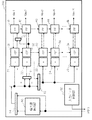
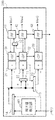
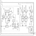
- FIG. 1 shows an example of the overall configuration of a peak detection circuit in a wireless communication system according to a first embodiment of the present invention.
- the peak detection circuit 200 of the present embodiment includes an input data control unit 50, adders 21 to 2k, sign determination units 31 to 3k, registers (FF (Flip Flop)) 41 to 4k, and a plurality of selection circuits 11, 12, 13 , 14 and a maximum value detector 60 are provided.
- the input data control unit 50 designates a storage position when the result of the correlation calculation is stored as input data. Accordingly, the input data control unit 50 may be, for example, an address generation unit that generates an address of a destination memory that stores the result of the correlation calculation as input data.
- the adders 21 to 2k add the value input from the selection unit 14 and the value input from the registers 41 to 4k. However, the adder 21 and the adders 23 to 2k invert the sign of the value from the selection unit 14 and input the values from the register 41 and the registers 43 to 4k as they are, and add them. That is, the adder 21 and the adders 23 to 2k subtract the value input from the selection unit 14 from the values from the register 41 and the registers 43 to 4k.
- the adder 22 adds the value input from the selection unit 11 and the value input from the register 42. As will be described later, the value from the selector 11 is input to the adder 22 as it is after being inverted by the setting of the control signal.
- the sign determiners 31 to 3k determine the sign of the output result of the adder.
- the determination results of the code determiners 31 to 3k are also output to the next-stage code determiner.
- the next stage means the direction from the code determiner 31 to the code determiner 3k.
- Registers 41 to 4k store peak values. Furthermore, the time information of the stored peak value, for example, the representative value at the time when the received data signal used for the correlation calculation is input, is also stored in association with each peak value.
- the storage means for storing the time information of each peak value is not particularly limited. For example, a part of the registers 41 to 4k that store corresponding peak values may store this time information.
- the registers 41 to 4k can shift the values stored in the registers to the next-stage registers. Whether or not to shift to the next stage is controlled by the sign of the outputs of the sign determiners 31 to 3k.
- the next stage means the direction from the register 41 to the register 4k.
- the selection circuits 11, 12, 13, and 14 select and output one of the two pieces of input information in accordance with a control signal (not shown) for setting the operation mode and the like. By switching the control signal, the internal configuration of the peak detection circuit can be changed and the processing content can be changed.
- the local maximum detector 60 detects a local peak.
- the control signal is input to the input data control unit 50 and the selection circuits 11, 12, 13, and 14 in common.
- the selection circuit 11 is a sign inversion / non-inversion selection circuit that selects whether or not the sign of the input data to the adder 22 is inverted by a control signal.
- the selection circuit 12 is a storage data selection circuit that switches data to be stored in the register 41 by a control signal.
- the selection circuit 13 is an output data selection circuit that switches output data to a subsequent adder according to a control signal.
- the selection circuit 14 is a maximum value detection processing selection circuit that selects whether or not input data is preprocessed by the maximum value detection unit according to a control signal.
- the selection circuit 11 and the adder 22 may be combined as an adder / subtracter.
- the values Max 1 to Max k stored in the registers 41 to 4k are the peak detection result data output as the desired peak detection results. is there.
- the maximum number of detectable peaks, that is, the maximum number of detection result data is k.
- the number of peaks to be actually detected can be set, and a clock and data gating mechanism may be provided so that a circuit in a portion not necessary for detecting the set number of peaks does not operate. For example, when three peaks are detected, the adders 24 to 2k, the sign determiners 34 to 3k, and the registers 44 to 4k that are used to detect the fourth and subsequent peaks are unnecessary. Alternatively, the maximum value detection unit 60 is not used in the later-described integration processing mode. In such a case, wasteful power consumption can be reduced by providing a gating mechanism.
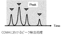
- FIGS. 2A and 2B are diagrams illustrating an example of peak detection processing in a plurality of general wireless communication systems.
- FIG. 2A in the case of CDMA or the like, when multipath occurs, a method of demodulating all received data signals having different arrival times and combining them is used. Therefore, it is necessary to obtain a plurality of peaks corresponding to the number of multipaths from the result of the cross-correlation operation between the received data signal and the known signal at each time.
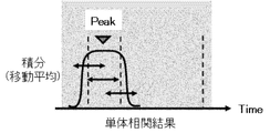
- the “integration process” is a process for obtaining the sum of the calculation results in a predetermined period (hereinafter referred to as “integration period”), and can also be referred to as “accumulation process”. Further, as will be described later, the integration result is only used for comparison with other integration results having different integration periods, and the value itself is not important.
- the length of the integration period is constant. Therefore, an average value may be obtained by dividing the integration result by the length of the integration period, and it may be used instead of the integration result. Since the integration process is performed by changing the integration period, this average value calculation process can also be called a “moving average process”.
- the process simply described as “integration process” may be “accumulation process” or “moving averaging process” unless otherwise specified.
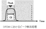
- 3A and 3B are diagrams illustrating integration processing in OFDM. Even in OFDM, there is a peak in the result of a single autocorrelation calculation. However, as shown in FIG. 2B, the peak value is ideally a constant value over the entire period corresponding to the GI length.
- the integration process of the single correlation result is performed for the GI length around each timing.
- a peak appears ideally at the center of the GI length. Therefore, a timing at which a peak appears is detected, and for example, the timing is set as an FFT (Fast Transform) process start timing at the time of OFDM reception.
- FFT Fast Transform
- the above-described peak detection processing with different processing contents in a plurality of wireless communication systems can be flexibly handled by reconfiguring the circuit. It is.
- FIG. 4 shows an operation in the multiple peak detection mode in which the peak detection circuit 200 shown in FIG. 1 detects peaks for a plurality of paths as shown in FIG. 2A at a time.
- the selection circuits 11, 12, 13, and 14 are set to the following states by the control signal in advance. 1)
- the selection circuit 14 selects the output of the maximum value detector 60.
- the input data control unit 50 sequentially issues addresses for reading the continuous correlation result data from the external memory. Accordingly, correlation result data is sequentially read from the memory.
- the selection circuit 14 selects the output of the maximum value detection unit 60.
- the local maximum value detection unit 60 obtains a local maximum value in the continuous correlation result data, that is, a local maximum value.
- the maximum value detection unit 60 outputs the correlation result data as it is when it is determined that the input correlation result data is larger than the preceding and following correlation result data and has a maximum value.
- a minimum value such as “all 0” is output.
- the data output from the selection circuit 14 is processed as follows by the adders 21 to 2k, the sign determination units 31 to 3k, and the registers 41 to 4k whose functions are set by the selection circuits 11, 12, and 13. . 2)
- the selection circuit 11 selects the inverting input ( ⁇ ).
- the selection circuit 11 selects and outputs the inverting input ( ⁇ ) in FIG. 3)
- the selection circuit 12 selects the input from the previous stage.
- the selection circuit 12 selects the input on the adder 21 and sign determination unit 31 side. Specifically, the maximum value stored in the register 41, that is, the correlation result data determined to be the maximum value by the maximum value detection unit 60 is selected. 4) The selection circuit 13 selects the correlation result data side.
- the adders 21 to 2k, the sign determiners 31 to 3k, and the registers 41 to 4k operate as follows.
- the adders 21 to 2k Since all the inputs of the adders 21 to 2k are numbers with inverted signs, the adders 21 to 2k all operate as subtractors. That is, all the adders 21 to 2k operate in parallel so as to subtract the same input data (correlation result data) from the respective values of the registers 41 to 4k storing the respective peak values. In this way, the sign determiners 31 to 3k determine the sign of the result of subtracting the data by the adders 21 to 2k. Then, the registers 41 to 4k update the peak values stored therein according to the results of the code determiners 31 to 3k.
- the adders 21 to 2k, the sign determination units 31 to 3k, and the registers 41 to 4k operate as k (1 to k) comparators and peak value storage registers, respectively. Further, as described above, the time information of the peak value stored in each of the registers 41 to 4k is stored by a predetermined storage unit corresponding to each peak value.
- the adder 21 subtracts the next input correlation result data from the peak value of the register 41.
- the sign determination unit 31 determines that the subtraction result is negative, it means that the correlation result data is larger than the peak value stored in the register 41.
- the value of the register 41 that is the maximum peak value is updated to the correlation result data and the timing when the subtraction result becomes negative.
- the values of the registers 41 to 4k are all shifted one by one, such that the value of the register 41 which has been the maximum so far is stored in the register 42, the value of the register 42 is stored in the register 43, and so on.
- the registers 41 to 4k store the inverted correlation result data input to the adders 21 to 2k, but the registers 41 to 4k actually store the data.
- the correlation result data is not inverted.
- the sign determination unit 31 determines that the subtraction result is positive, it means that the peak value stored in the register 41 is larger than the correlation result data, so the value of the register 41 is updated. Not.
- the above-described series of processing for updating the peak value of the correlation result data is realized by operating the adders 21 to 2k, the code determiners 31 to 3k, and the registers 41 to 4k arranged in parallel in parallel. To do. As a result of the processing, the data are stored in the register 41, the register 42, the register 43,.
- the input correlation result data is smaller than the peak value stored in the register 42 but larger than the peak value stored in the register 43.
- the value of the register 43 is updated with the input correlation result data and the timing thereof, and the values of the registers 44 to 4k subsequent to the register 43 are sequentially shifted to the register 45 and the subsequent stages.
- the value shifted from the register 4k may be discarded.
- the register values at each stage are manipulated as follows according to the sign determination results by the sign determiners 31 to 3k.
- the sign determination result is negative in both the preceding stage and the own stage, the value of the register in the own stage is shifted from the previous stage value.
- the previous stage data is shifted to its own stage. come. For this reason, the subsequent stage data is always smaller than the previous stage data, so that “the sign determination result of the preceding stage is negative and the sign determination result of the own stage is not positive”.
- FIG. 5 shows the operation in the integration processing mode in which the peak detection circuit 200 shown in FIG. 1 detects the maximum peak after the integration processing as shown in FIGS. 2B and 3B. .
- the integration result at a certain timing T when the integration processing for the OFDM GI length is performed is “T ⁇ (0.5 ⁇ GI length) to T + (0.5 ⁇ GI length). ) "Correlation result data are added together.
- the integration result at the timing T is obtained by subtracting the correlation result data at the timing of (T-1-0.5 ⁇ GI length) from the integration result at the previous timing (T ⁇ 1) to obtain (T + 0.5 ⁇ GI length).
- Timing correlation result data is also added.
- the subtracters corresponding to two comparators for a plurality of paths shown in FIG. Are used as adders and subtracters for integration processing.
- the selection circuits 11, 12, 13, and 14 are set to the following states in advance by the control signal. 1)
- the selection circuit 14 selects the output of the memory.
- the selection circuit 14 is set to select the output of the memory instead of the output of the maximum value detector 60 by the control signal. Therefore, the selection circuit 14 outputs the input correlation result data as it is.
- the input data control unit 50 issues an address for reading from the memory. For example, when integrating the correlation result data centered on the timing T, the input data control unit 50 calculates the correlation result data at the timing of (T-1-0.5 ⁇ GI length) and (T + 0.5 ⁇ The memory address for storing each of the correlation result data of the timing of (GI length) is issued. At the next timing (T + 1), the correlation result data is continuously read from the memory by issuing addresses added by one each.
- the data output from the selection circuit 14 is processed as follows by the adders 21 to 23, the sign determination units 31 to 33, and the registers 41 to 43 whose functions are set by the selection circuits 11, 12, and 13. . 2)
- the selection circuit 11 selects the non-inverting input (+).
- the selection circuit 11 selects and outputs the non-inverting input (+) in FIG. 3)
- the selection circuit 12 selects an input from the subsequent stage.
- the selection circuit 12 selects an input from the subsequent stage. Specifically, the integration result stored in the register 41, that is, the output of the adder 22 is selected. As will be described later, the selection circuit 12 may temporarily select the output of the adder 21 in order to store the output of the adder 21 in the register 41 as intermediate data. Alternatively, the output of the adder 21 may be output to the register 41 and stored in a path different from the selection circuit 12. 4) The selection circuit 13 selects the input from the adder 22.
- the selection circuit 13 selects the input from the adder 22, that is, the integration result data.
- the adder 21 and the adder 22 operate as an integration processing subtracter and adder, respectively.
- the register 41 stores integration result data at each timing.
- the adder 23, the sign determination unit 33, and the register 43 in the subsequent stage operate as a comparator and a peak value storage register for maximum peak detection processing.
- the input data of the adder 23 is not the read correlation result data but the integration result data from the adder 22.
- the adder 21 subtracts the correlation result data at the timing of (T-1-0.5 ⁇ GI length) from the integration result data at the timing (T ⁇ 1) stored in the register 41, and registers the register 41 as intermediate data. Write back to At this time, the selection circuit 12 temporarily selects the output of the register 41.
- the adder 22 adds the correlation result data of the next input timing (T + 0.5 ⁇ GI length) to the intermediate data stored in the register 41.
- the intermediate data stored in the register 41 is input to the adder 22 by inputting to the adder 22 through a predetermined path (not shown), for example, a selection circuit that selects the outputs of the register 41 and the register 42.
- the integration result at timing T is obtained by the above calculation.
- the integration result data is transferred to the adder 23 side in the subsequent stage via the selection circuit 13.
- the integration result data is also stored in the register 41 via the selection circuit 12 for integration processing at the next timing (T + 1). Therefore, the stored contents of the register 41 alternately change in time between the intermediate data and the final integration result.
- the integration result data at the next input timing is subtracted from the peak value stored in the register 43 as in the case of FIG.
- the sign determination unit 33 determines that the subtraction result is negative, it means that the integration result data is larger than the peak value stored in the register 43. Therefore, the value of the register 43, which is the maximum peak value, is updated with the integration result data and its timing.
- the sign determination unit 33 determines that the subtraction result is positive, it means that the peak value stored in the register 43 is larger than the integration result data, so the value of the register 43 is updated. Not.
- the adder 21, the adder 22, and the register 41 which are used as two comparators corresponding to the number of multiple paths in the multiple peak detection mode, are the subtractor, adder, Used as integration result storage register.
- the adder 23, the sign determination unit 33, and the register 43 in the subsequent stage operate as a peak detection comparator and a peak value storage register, as in the multiple peak detection mode.
- the peak detection circuit according to the present embodiment includes various selection circuits therein, whereby the common arithmetic unit can be reconfigured as a processing circuit corresponding to different communication methods. That is, a common circuit can be reconfigured according to the value of the control signal for setting the mode.
- the common adders 21 and 22, the register 41, and the like can be set to operate as a comparator and a peak value storage register for peak detection processing for obtaining a plurality of peaks.
- it can be set to operate as a subtracter or adder for integration processing and an integration result storage register required in a wireless communication system such as OFDM.
- a common circuit can be shared by a plurality of processes.
- one circuit can flexibly cope with various peak detection processes that differ between different communication systems such as CDMA and OFDM, and can support a plurality of communication systems with a smaller circuit scale.
- the arithmetic unit can be shared by a plurality of processes with a small circuit overhead such as a selection circuit, the circuit scale is reduced as compared with the case where each method is realized using individual circuits.
- the peak detection circuit of the present invention can be used efficiently with various peak detection methods. can do.
- the minimum configuration that the peak detection circuit of this embodiment should have is three sets of processing circuits for each stage including an adder, a sign determination unit, and a register, four selection circuits, It is a local maximum detector.
- An input data control unit for generating a memory address may be provided outside.
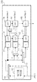
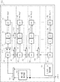
- FIG. 6 is a block diagram showing the configuration of the peak detection circuit 210 when the number k of detection result data is three in the peak detection circuit of this embodiment.
- 7A and 7B are block diagrams showing the operation of the peak detection circuit 210 in the multiple peak detection mode and the integration processing mode, respectively.
- FIGS. 1, 4, 5, and 6 blocks that control basic functions such as data selection, data addition / subtraction, and determination of the sign of the calculation result are individually shown.
- HDL Hardware Description Language
- circuit design using HDL which is often used, it is possible to design a circuit only by defining the function, and it is not necessary to clarify the specific configuration of the circuit. Circuit description is possible.
- the essential configuration of the present embodiment is the peak detection circuit 220 shown in FIG. That is, the selection circuit is not explicitly provided, and the addition function and the comparison function that can be realized by the adder and the sign determination unit can be abstracted as an arithmetic unit.
- the peak detection circuit 220 includes operation units 101, 102, 103 and registers 104, 42, 43.
- the calculation unit 101 has a function in which the selection unit 14, the adder 21, and the sign determination unit 31 are integrated. That is, the calculation unit 25 selects input data or output data of the local maximum value detection unit 60 by the control signal, subtracts the selected data from the value from the register 104, and outputs the sign of the subtraction result.
- the calculation unit 102 has a function in which the selection units 11 and 14, the adder 22, and the sign determination unit 32 are integrated. That is, the calculation unit 102 selects input data or the output of the maximum value detection unit by the control signal, and calculates the selected data and the value from the register 42. This calculation is the subtraction of the selected data from the value from the register 42 or the addition of the value from the register 42 and the selected data, and the selection is performed according to the control signal. Then, the sign of the calculation result is output.
- the calculation unit 103 has a function in which the selection units 13 and 14, the adder 23, and the sign determination unit 33 are integrated. That is, the calculation unit 103 selects the input data, the output of the maximum value detection unit 60, or the calculation result of the calculation unit 102 by the control signal, subtracts the selected data from the value from the register 43, and further, the sign of the subtraction result Is output.
- the processing target data is assumed to be data (correlation result data) as a result of correlation calculation of synchronization processing in communication.
- the contents and attributes of the data to be processed do not depend on the operation of the peak detection circuit of this embodiment. Therefore, the present embodiment can be applied to the case where the following two types of processing are performed on data obtained as a result of general processing.
- Applicable first processing is processing for obtaining a peak within a certain period for a predetermined processing result, and corresponds to the “multiple peak detection processing” of the present embodiment.
- the applicable second process is a process for obtaining a maximum value of integration (accumulation, moving average) and integration result over a certain period for a predetermined process result, and corresponds to the “integration process” of the present embodiment. Is.
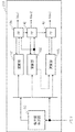
- FIG. 9 shows a block configuration of a peak detection circuit according to the second embodiment of the present invention.
- a specific configuration of a local maximum detection unit that can be shared in local maximum detection processing and integration processing is shown.
- the peak detection circuit 201 in the second embodiment includes an input data control unit 51, a maximum value detection unit 61, and a peak detection unit 62.
- the peak detector 62 includes adders 23 to 2k + 2 for comparing with the number of peaks corresponding to the number of multipaths, sign determiners 33 to 3k + 2, and registers 43 to 4k + 2 for storing the peak value and its timing. After processing all correlation result data (input data), finally, the values Max 1 to Max K stored in the registers 43 to 4k + 2 are output as desired peak (timing) detection results. It is peak detection result data. In this way, in the second embodiment, k pieces of peak detection result data are stored in the registers 43 to 4k + 2.
- the second embodiment does not include the adders 21 and 22, the sign determination units 31 and 32, and the registers 41 and 42 that are provided in the first embodiment.
- the peak detection function processed by the adders 21 and 22, the sign determiners 31 and 32, and the registers 41 and 42 is the adders 23 and 24 and the sign determiners 33 and 34 in the second embodiment.
- the integration function processed by the adders 21 and 22, the sign determination units 31 and 32, and the registers 41 and 42 in the first embodiment is processed by the maximum value detection unit 61 in the second embodiment.
- k circuits are mounted in parallel in the peak detection unit 62 corresponding to a plurality of peaks k that need to be detected at one time assuming CDMA or the like.
- the peak detector 62 can detect a plurality of peaks up to a maximum of k. However, the number k of peaks that are actually detected during operation can be set, and a circuit that is not necessary is not operated. And a data gating mechanism or the like. By providing the gating mechanism, useless power consumption can be reduced.
- the local maximum detection unit 61 includes adders 71 and 72, sign determination units 81 and 82, registers (FF) 91 and 92, selection circuits 15, 16, 17, 18 and 19, and a logical product (AND) circuit 20.
- the configuration peculiar to the second embodiment includes selection circuits 15, 16, 17, and 18 that can select whether the maximum value detection unit 61 operates in the multiple peak detection mode or the integration processing mode. It is. This selection is realized by inputting a control signal for setting a mode to the local maximum detector 61. Although not shown, the control signal is commonly connected to the input data control unit 51 and the selection circuits 15, 16, 17, and 18. As will be described later, the selection circuit 19 is a selection circuit used to select data to be stored in the register 92 in the integration processing mode, and is not controlled by a control signal.
- the adders 71 and 72 and the sign determiners 81 and 82 are used for maximum value determination processing or integration processing.
- the registers 91 and 92 store input correlation result data and integration result data.
- the selection circuit 15 is a sign inversion / non-inversion selection circuit for switching the sign of the input correlation result data for reconfiguring the local maximum detection unit 61 by the control signal.
- the selection circuit 16 is an input data selection circuit that switches input data to the adder 71.
- the selection circuit 17 is a storage data selection circuit that switches output data to the register 92.
- the selection circuit 18 is an output data selection circuit that switches output data to the peak detection unit. As will be described later, the selection circuit 18 selects the local maximum value or the integration result data and outputs it to the peak detector 62.
- the selection circuit 18 corresponds to the selection circuit 14 in FIG. 1 when the local maximum value is selected.
- the selection circuit 18 corresponds to the selection circuit 13 in FIG. 1 in the sense that when the integration result data is selected, it is output to the adder 23 in the subsequent stage.
- the AND circuit 20 masks the output value of the correlation result data depending on whether or not the value held in the register 91 is a maximum value. Whether or not it is a maximum value is indicated by a maximum value detection signal max that is output based on the outputs of the sign determiners 81 and 82. For example, when the value input to one input terminal is a maximum value, the AND circuit 20 sets the other input, that is, the maximum value detection signal max to the maximum value (such as “all 1”), and sets the maximum value. Output as is. When the value input to one input terminal is not the maximum value, the AND circuit 20 sets the maximum value detection signal max to the minimum value (such as “all 0”) and outputs the minimum value.
- the selection circuit 15 and the adder 72 may be combined and mounted as an adder / subtracter.
- the operation of the second embodiment will be described with reference to FIGS.
- the second embodiment also supports three types of peak detection methods in order to support a plurality of wireless communication systems.
- the first peak detection method is the simplest peak detection method for detecting one maximum value.
- the second peak detection method is a multiple peak detection method that detects a plurality of multipath timings at a time, such as CDMA, and corresponds to the “multiple peak detection mode” processing in the first embodiment.
- the third peak detection method is a method of detecting one peak after performing integration processing such as OFDM, and corresponds to the processing of the “integration processing mode” in the first embodiment.
- the selection circuits 15, 16, 17, and 18 of the maximum value detection unit 61 in the peak detection circuit 201 are controlled and reconfigured.
- FIG. 10 shows that the peak detection circuit 201 shown in FIG. 9 detects the peaks for the number of multiple paths as shown in FIG. 2A at the same time as in the first embodiment. It is a figure which shows the operation example in the case of doing. This technique is often used in CDMA and the like.
- a necessary circuit is set in advance to a state for detecting in parallel peaks corresponding to the number of multiple paths by a control signal.
- the selection circuits 15, 16, 17, and 18 in the maximum value detection unit 61 perform the selection operation as follows. At this time, the adders 71 and 72 operate as a subtracter for detecting the maximum value. 1) The selection circuit 15 selects the inverting input ( ⁇ ). 2) The selection circuit 16 selects the correlation result data read from the memory. 3) The selection circuit 17 selects the output of the register 91. 4) The selection circuit 18 selects the output of the AND circuit 20.
- the input data control unit 51 sequentially issues addresses for reading continuous correlation result data from the memory. Then, by controlling a control signal for setting the mode of the peak detection method, the maximum value detection unit 61 detects whether or not the correlation result data before and after is a maximum value.
- the correlation result data of the timing T is used as the timings before and after (T ⁇ 1 and T + 1).
- a method for comparing with the correlation result data that is, a method for comparing locally.
- peaks corresponding to the number of multiple paths are detected from the correlation result data having a locally large value, that is, a local maximum value. This is because if peak detection is performed between correlation result data for all timings, consecutive timings near the maximum value that should be treated as one peak are erroneously detected as a plurality of peaks.
- the sign inverting circuit 15 of the input correlation data of the local maximum value detection unit 61 selects the inverting input ( ⁇ ).
- the selection circuit 16 selectively outputs the input correlation result data.
- the selection circuit 17 selects the correlation result data of the register 91, and the register 92 stores the data. Further, the selection circuit 18 outputs the correlation result data of the register 91 masked by the AND circuit depending on whether or not it is a local maximum value.
- the adders 71 and 72 and the sign determination units 81 and 82 are comparators (subtracters and sign determinations) for comparing the correlation result data at a certain timing T with the correlation result data at the preceding and following timings, respectively.
- the correlation result data input from the memory is sequentially shifted to the register 91 at the next timing, and further to the register 92 at the next timing. Accordingly, the correlation result data is input to the adders 71 and 72 by being shifted by one timing by the registers 91 and 92.
- the correlation result data at a certain reception timing T is stored in the register 91
- the correlation result data at the reception timing (T ⁇ 1) is stored in the register 92 by the selection circuit 17.
- the correlation result data at the next reception timing T + 1 is input from the memory, and the correlation result data at the reception timing T + 1 is input to the adder 71 by the selection circuit 16.
- the adders 71 and 72 and the sign determination units 81 and 82 the correlation result data of the reception timing T stored in the register 91 and the two correlation result data of the preceding and succeeding timings are simultaneously processed. Is called.
- both the adders 71 and 72 operate as subtracters because the sign of the correlation result data at the reception timing T is inverted. That is, the adder 71 subtracts the timing T data from the timing (T + 1) data, and at the same time, the adder 72 subtracts the timing T data from the timing (T ⁇ 1) data.
- the maximum value detection signal max is set to a maximum value (such as “all 1”). Therefore, in this case, the correlation result data of the reception timing T stored in the register 91 is output to the peak detection unit 62 as it is without being masked.
- the maximum value detection signal max is set to a minimum value (such as “all 0”). Therefore, in this case, the correlation result data at the reception timing T is masked by the AND circuit 20, and a minimum value such as all 0 is output to the peak detector 62.
- the peak detection part 62 it is the same as that of the case where the several peak in 1st Embodiment shown in FIG. 4 is detected. That is, using the adders 23-2k + 2 and the sign determiners 33-3k + 2, parallel comparison processing between the correlation result data input from the local maximum value detection unit 61 and the plurality of peak values stored in the registers 43-4k + 2 is performed. Do. At this time, the values are stored in the register 43, the register 44, and the register 45 in order from the largest peak value, and the adders 23 to 2k + 2 all operate as subtracters because the input data is sign-inverted. All the adders 23 to 2k + 2 operate in parallel so as to subtract the same input data (correlation result data) from the respective values of the registers 43 to 4k + 2 storing the respective peak values.
- the sign judgment of the result of subtraction by the sign judgment units 33 to 3k + 2 is performed. For example, when the value of the register 44 is larger in the second-stage code decision unit 34, the input correlation result data is larger in the third-stage code decision unit 35 (not shown in FIG. 10). The correlation result data is stored in the register 45 as the third stage peak value. Then, the values of the subsequent registers 46 to 4k + 2 are shifted to the next register. That is, similar to the operation in the first embodiment shown in FIG. 4, these operate as k (1 to k) comparators and peak value storage shift registers.
- the control circuit is used to control the selection circuits 15, 16, 17, and 18 so that the local maximum value detection unit 61 detects whether each correlation result data is a local maximum value. It is possible to operate as a multiple peak detection mode.
- FIG. 11 shows an operation example when the peak detection circuit 201 shown in FIG. 9 detects the maximum peak after the integration processing as shown in FIGS. 2B and 3B. This technique is often used for OFDM and the like.
- an address for reading the correlation result data from the memory is issued. That is, for example, when integrating the correlation result data centered on a certain timing T, the input data control unit 51 calculates the correlation result data at the timing of (T-1-0.5 ⁇ GI length) and (T + 0.5 The correlation result data at the timing of ( ⁇ GI length) is read from the memory. At the next timing (T + 1), the correlation result data is continuously read from the memory by issuing addresses incremented by +1.
- FIG. 11 which is the second embodiment, the maximum value detection process is not necessary and the integration process is necessary. 15, 16, 17 and 18 are controlled. Thereby, the local maximum detection unit 61 operates in the integral processing mode.
- the selection circuits 15, 16, 17, and 18 in the maximum value detection unit 61 perform the selection operation as follows.
- the adders 71 and 72 operate as a subtracter and an adder for performing integration processing, respectively.
- the register 92 stores integration result data at each timing. 1)
- the selection circuit 15 selects the non-inverting input (+). 2)
- the selection circuit 16 selects the integration result data stored in the register 92.
- the selection circuit 17 selects the integration result data that is the output of the adder 72.
- the selection circuit 18 selects the integration result data that is the output of the adder 72.
- the adder 72 adds the correlation result data of the timing (T + 0.5 ⁇ GI length) stored in the register 91 that is input next to the intermediate data stored in the register 92, thereby integrating at the timing T. Results are required.
- the integration result data is transferred to the peak detection unit 62 at the subsequent stage and is also stored in the register 92 for integration processing at the next timing (T + 1).
- the register 92 stores the intermediate data from the adder 71 or the integration result from the adder 72.
- the selection circuit 19 selects whether the data from the adder 71 or the adder 72 is stored in the register 92. Accordingly, the selection content of the selection circuit 19 dynamically changes appropriately during the processing in the integration processing mode.
- the adder 23 subtracts the integration result data at the next input timing from the peak value stored in the register 43.
- the sign determination unit 33 determines that the subtraction result is negative, the integration result data is larger than the peak value stored in the register 43, and therefore the value of the register 43 that is the maximum peak value. Is updated to the integration result data and its timing.
- the sign determination unit 33 determines that the subtraction result is positive, the peak value stored in the register 43 is larger than the integration result data, so the value of the register 43 is not updated.
- the second embodiment does not include the adders 21 and 22 and the sign determination units 31 and 32 of the first embodiment.
- the integration process is performed using the maximum value detection unit 61. This point is different from the first embodiment in which integration processing is performed using the adder 21 and the sign determination unit 31.
- the above peak detection processing is repeated for the correlation result data (integration result data) for all timings to be detected. Then, the desired peak detection result (MAX) is finally stored in the register 43. That is, the maximum peak value after integration processing and its timing can be acquired.
- the present embodiment is not limited to the configuration shown in FIGS. That is, the input data processing unit 51 may be provided outside. Further, the number of stages comprising an adder, a sign determination unit, and a register constituting the peak detector 62 may be one if the number of peaks obtained in the multiple peak detection mode is one. Further, the data to be processed is not limited to data as a result of correlation calculation of synchronization processing in communication. (Effect of 2nd Embodiment) As described above, in the second embodiment, the selection contents of the selection circuits 15, 16, 17, and 18 of the maximum value detection unit 61 are set according to the peak detection method by the control signal.
- the adder 71, the adder 72, and the register 92 used as the comparator for detecting the maximum value and the correlation result data storage register in FIG. 10 are the subtractor and adder for integration processing in FIG. 11, respectively. , Used as an integration result data storage register. This sharing can be realized by providing the selection circuits 15, 16, 17, and 18 for reconfiguration.
- the circuit scale is reduced as compared with the case where individual circuits are provided for each peak detection method, that is, when both the maximum value detection circuit and the integration processing circuit are provided. Is done. Therefore, a plurality of types of peak detection methods can be efficiently handled with fewer circuits.
- comparators adders 71 and 72 and sign determiners 81 and 82 for determining whether or not the maximum value is used as preprocessing when detecting a plurality of peaks in CDMA or the like, and a register for shifting correlation result data
- a selection circuit is provided so that it can be shared as an adder or subtracter in the integration processing in OFDM and an integration result storage register. For this reason, the circuit scale can be reduced as compared with the case where additional circuits for integration processing are additionally mounted.
- the adder is used as a subtracter for detecting a maximum value in advance when obtaining a plurality of peaks by CDMA or the like.
- the adder is used as an adder for integration processing in OFDM or the like. That is, in the example of the second embodiment shown in FIG. 9, it is possible to switch between using a common adder as a subtractor for detecting a maximum value or an adder for integration processing. . Thereby, the peak detection part 62 which performs the peak detection of a back
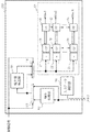
- FIG. 12 is a block diagram showing a specific example of the peak detection circuit according to the third embodiment of the present invention.
- the third embodiment when a plurality of peaks are detected, comparison processing with each peak value is sequentially performed in a pipeline manner.
- the peak detection circuit 202 includes an input data control unit 50, adders 21 to 2k, sign determiners 31 to 3k, and registers. 41 to 4k, and a local maximum detector 60 is provided.
- the functions of the above blocks are the same as those in the first embodiment, and a description thereof will be omitted.
- a configuration unique to the third embodiment includes registers 91 to 9k, selection circuits A1 to Ak-1, selection circuits 111 and 14, and a selection control circuit 112.
- Registers 91 to 9k are used to sequentially perform comparison processing with a plurality of peaks in a pipeline manner.
- the selection circuits 111 and 14 and the selection control circuit 112 are selection circuits for reconfiguring the arithmetic unit by a control signal (not shown) for setting the peak detection processing mode and the like.
- the control signal is also input in common to the input data control unit.
- the selection circuit 111 is a sign inversion / non-inversion selection circuit that selects whether or not to invert the sign of the input data to the adder 21 by a control signal in which an operation mode or the like is set.
- the selection control circuit 112 is a selection control circuit that designates selection of data to be input to the selection circuit A1 by a control signal.
- the selection circuit 14 is a maximum value detection processing selection circuit that selects whether or not input data is preprocessed by a maximum value detection unit according to a control signal. Note that the selection circuit 111 and the adder 21 may be implemented together as an adder / subtracter.
- the selection circuit A1 selects the value of the register 91 or the register 41 according to the instruction of the selection control circuit 112.
- the selection circuits A2 to Ak-1 respectively set the value of the register 91 or the register 41, the value of the register 92 or the register 42, ..., the value of the register 9k-1 or the register 4k-1 in accordance with an instruction from the control signal. select.
- the peak detection result data (Max 1 to Max K) is desired in the registers 41 to 4k. Is stored as a peak (timing) detection result.
- the peak detection circuit 202 is set to the multiple peak detection mode using the control signal. In the multiple peak detection mode, the peak detection circuit 202 detects a plurality of peaks in a pipeline manner.
- the peak detection circuit 202 operates in the integration processing mode. In the integration processing mode, the peak detection circuit 202 obtains one peak after performing integration processing for the GI length.
- the third embodiment differs from the first embodiment in that, when obtaining peaks for a plurality of paths, the comparison processing with each peak value for a certain correlation result data is not performed in parallel, but in a pipeline. Is to perform the process automatically. That is, in the third embodiment, processing is sequentially performed in a pipeline manner while storing the correlation result data in the registers 91 to 9k and shifting to the next-stage register.
- the number of peaks to be actually detected can be set, and the clock and data gates are not operated so that the circuits not necessary for detecting the set number of peaks do not operate.
- a ting mechanism or the like may also be provided.
- the maximum value detection unit 60 is not used in the integration processing mode. In such a case, wasteful power consumption can be reduced by providing a gating mechanism.
- the selection circuits 14 and 111 and the selection control circuit 112 are set to the following states in advance by the control signal. 1)
- the maximum value detection control circuit 14 selects the output of the maximum value detection unit 60.
- the input data control unit 50 sequentially issues addresses for reading continuous correlation result data from the memory. Accordingly, correlation result data is sequentially read from the memory.
- the selection circuit 14 selects the output of the maximum value detection unit 60.
- the maximum value detecting unit 60 obtains a maximum value in continuous correlation result data.
- the maximum value detection unit 60 outputs the correlation result data as it is when it is determined that the input correlation result data is larger than the preceding and following correlation result data and has a maximum value. When it is determined that the input correlation result data is smaller than any of the preceding and following values and not a maximum value, a minimum value such as “all 0” is output. 2)
- the selection circuit 111 selects the inverting input ( ⁇ ). 3)
- the selection control circuit 112 selects the determination result signal of the sign determination unit 31 as a selection signal to the selection circuit A1.
- the data output from the selection circuit 14 is processed as follows by the adders 21 to 2k, the sign determination units 31 to 3k, and the registers 41 to 4k whose functions are set by the selection circuit 111 and the selection control circuit 112.
- the adders 21 to 2k Since all the inputs of the adders 21 to 2k are numbers with inverted signs, the adders 21 to 2k all operate as subtractors. Further, all adders 21 to 2k subtract the input data (correlation result data) stored in the registers 91 to 9k of the respective pipeline stages from the values of the registers 41 to 4k storing the respective peak values. To work. That is, the adders 21 to 2k, the sign determiners 31 to 3k, the registers 41 to 4k, and the selection circuits A1 to Ak-1 operate in a pipeline as a plurality of peak detection processing units for k stages. Further, as described above, the time information of the peak value stored in each of the registers 41 to 4k is stored by a predetermined storage unit corresponding to each peak value.
- the adder 21 subtracts the correlation result data (the value of the register 91) input next from the peak value of the register 41.
- the sign determination unit 31 determines that the subtraction result is negative, it means that the correlation result data is larger than the peak value stored in the register 41.
- the value of the register 41 is updated with the correlation result data and its timing, and at the same time, the value stored in the register 41 is output as output data to the register 92 at the next stage.
- the sign determination unit 31 determines that the subtraction result is positive, it means that the peak value stored in the register 41 is larger than the correlation result data. In this case, the value of the register 41 is not updated, and the correlation result data of the register 91 is output as it is to the register 92 of the next stage.
- the selection circuit A1 to Ak-1 selects the value to be output to the next-stage register, that is, the subtraction result or the previous-stage register value, and the determination results of the sign determiners 31 to 3k-1 follow the instructions.
- ⁇ Perform the above processing in a pipeline while continuously inputting correlation result data at each reception timing. That is, a peak detection processing unit for k stages including registers 91 to 9k, adders 21 to 2k, sign determination units 31 to 3k, peak value storage registers 41 to 4k, selection circuits A1 to Ak, and the like are pipelined. Operate. By this operation, comparison processing is performed in order from a large peak value for arbitrary correlation result data.
- the peak detection processing unit in the first stage of the peak detection circuit 202 is used as the integration processing unit. Make it work.
- the selection circuits 14 and 111 and the selection control circuit 112 are set to the following states in advance by the control signal. 1)
- the selection circuit 14 selects the output of the memory.
- the selection circuit 14 is set to select the output of the memory instead of the output of the maximum value detection unit 60 according to the control signal. Therefore, the selection circuit 14 outputs the input correlation result data as it is.
- the input data control unit 50 issues an address for reading from the memory.
- the input data control unit 50 obtains the address for reading the correlation result data of the timing (T-1-0.5 ⁇ GI length) and the correlation result data of the timing (T + 0.5 ⁇ GI length) from the memory. Issue. Then, at the next timing (T + 1), the correlation result data is continuously read from the memory by issuing addresses added by one each. 2)
- the selection circuit 111 is set to the dynamic control mode.
- the selection circuit 111 dynamically changes the selection of the non-inverting input (+) or the inverting input ( ⁇ ) according to the dynamic control mode, that is, whether the processing performed by the adders 21 to 2k is addition or subtraction. Set to mode. 3)
- the selection control circuit 112 selects the value of the register 41 in a fixed manner.
- the selection signal control circuit 112 is set so as to always output the value of the register 41 as output data from the selection circuit A1.
- the data output from the selection circuit 14 has the functions set by the selection circuit 111 and the selection control circuit 112, adders 21 to 2k, sign determination units 31 to 3k, registers 41 to 4k, selection circuits A1 to Ak-1. Is processed as follows.
- the adder 21 operates alternately as a subtracter and an adder for integration processing.
- the register 41 stores integration result data at each timing.
- the adder 22, the sign determination unit 32, and the register 42 in the subsequent stage operate as a comparator and peak value storage register for maximum peak detection processing.
- the input data of the adder 22 is always integration result data stored in the register 41.
- the adder 21 subtracts the correlation result data at the timing (T-1-0.5 ⁇ GI length) stored in the register 91 from the integration result data at the timing (T ⁇ 1) stored in the register 41. Then, it is written back to the register 41 as intermediate data for integration processing.
- the adder 21 adds the correlation result data of the timing (T + 0.5 ⁇ GI length) next input to the register 91 to the intermediate data stored in the register 41, and integrates at the timing T Find the result.
- the register 41 stores the integration result data for integration processing at the next timing (T + 1).
- the integration result data is output to the register 92 at the next stage and stored in the register 92.
- the calculation by the adder 21 is switched to addition or subtraction depending on the timing. This switching is performed by the selection circuit A1 dynamically changing the selection of the non-inverting input (+) or the inverting input ( ⁇ ).
- the integration result data at the next timing stored in the register 92 is subtracted from the peak value stored in the register 42.
- the sign determination unit 33 determines that the subtraction result is negative, it means that the integration result data is larger than the peak value stored in the register 42.
- the value of the register 42 which is the maximum peak value is updated with the correlation result data and its timing.
- the determination result in the sign determination unit 32 is positive, it means that the peak value stored in the register 42 is larger than the integration result data, so the value in the register 42 is not updated.
- the calculation by the adder 21 and the transfer of the calculation result to the next stage, the calculation by the adder 22 and the storage of the calculation result by the register 42 are performed in a pipeline manner.
- the selection circuits 111 and 14 and the selection control circuit 112 are controlled by the control signal.
- the first stage adder 21 and the sign determination unit 31 in the processing unit circuit of each stage configured by an adder, a sign determination unit, and a register that detect a plurality of peaks
- the integration processing mode it operates as a subtracter or adder.
- the register 41 operates as an integration result data storage register.
- the adder 22, the sign determination unit 32, and the register 42 in the next stage operate as a normal peak value detection circuit.
- the third-stage adder 23, sign determination unit 33, and register 43 operate as a normal peak value detection circuit.
- the fourth and subsequent stages operate as a normal peak value detection circuit. Therefore, if the number of detected peaks is one, only the first and second stage adders, sign decision units, registers, and selection circuits for selecting their input / output data are required. The adder, sign determination unit, register, and selection circuit are unnecessary. That is, the minimum configuration of the present embodiment is the first stage adder 21, sign determination unit 31, register 41, 91, second stage adder 22, sign determination unit 32, registers 42 and 92, and local maximum.
- the present embodiment is not limited to the configuration shown in FIG. That is, the input data processing unit 51 may be provided outside.
- the number of stages comprising an adder, a sign determination unit, and a register constituting the peak detection circuit may be a minimum of two.
- the data to be processed is not limited to data as a result of correlation calculation of synchronization processing in communication.
- the peak detection circuit 202 in the third embodiment a plurality of peaks are detected in a pipeline manner with respect to correlation result data at successive timings, and a peak detection process in a pipeline manner after the integration processing. It is possible to handle both cases. This can be realized by providing the selection circuits 111 and 14 and the selection control circuit 112 for reconfiguration.
- the arithmetic unit can be shared with less circuit overhead.
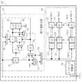
- FIG. 13 is a block diagram showing a specific example of a peak detection circuit according to the fourth embodiment of the present invention.
- an integration processing unit and a maximum value detection unit are provided for each of the two types of peak detection method modes, and only the peak detection processing unit is shared.
- the peak detection circuit 203 in the fourth embodiment of the present invention includes an input data control unit 50, a maximum value detection unit 61 that detects a maximum value, and a plurality of peaks in parallel.
- a detectable peak detector 62 is provided.
- the peak detector 62 includes adders 21 to 2k, sign determiners 31 to 3k, registers 41 to 4k for storing peak values, and the like for comparing the peak values for the number of multipaths with the input peak values. Prepare.
- the registers 41 to 4k may also store time information of peak values. Since the functions of the above blocks are the same as those in the first to third embodiments, description thereof will be omitted.
- an integration processing unit 63 for performing peak value integration processing assuming OFDM or the like is individually provided.
- the peak detection unit 203 includes selection circuits 113 and 14 that select the outputs of the integration processing unit 63 and the maximum value detection unit 61 according to a control signal for setting a processing mode in accordance with a wireless communication method to be processed and a peak detection method. Prepare.
- the selection circuit 113 is an integration processing selection circuit that selects whether or not to perform integration processing on the input correlation result data.
- the selection circuit 14 is a maximum value detection process selection circuit that selects whether or not to perform a maximum value detection process.
- the peak detector 62 may be provided with registers 91 to 9k and the like to detect a plurality of peaks in a pipeline manner, as in the third embodiment shown in FIG.
- the number of peaks to be actually detected can be set, and the clock and data gates are not operated so that the circuits not necessary for detecting the set number of peaks do not operate.
- a ting mechanism or the like may also be provided.
- the maximum value detection unit 60 or the integration processing unit 63 is not used depending on the processing content set by the control signal. In such a case, wasteful power consumption can be reduced by providing a gating mechanism.
- each input correlation result data is a local maximum value before detecting peaks corresponding to the number of multiple paths.
- the selection circuits 113 and 14 are set to correspond to the multiple peak detection mode.
- the data to be processed passes through the integration processing unit 63.
- the maximum value detection unit 60 performs a maximum value detection process on the data to be processed.
- the input data control unit 50 sequentially issues addresses for reading continuous correlation result data from the memory.
- the maximum value detection unit 60 determines whether or not the input correlation result data is a maximum value. For the correlation result data determined to be the maximum value, a plurality of peak values are detected in parallel by the peak detector 62.
- the selection circuits 113 and 14 are set so as to correspond to the integration processing mode.
- the integration processing unit 63 performs integration processing on the data to be processed. Then, the data that has been subjected to the integration process passes through the maximum value detection unit 60.
- the input data control unit 50 obtains an address for reading the correlation result data of timing (T-1-0.5 ⁇ GI length) and the correlation result data of timing (T + 0.5 ⁇ GI length) from the memory. A continuous address is sequentially issued as the start address. Then, the integration processing unit 63 performs integration processing using the input correlation result data, and the peak detection unit 62 detects the maximum peak value for the integration result data subjected to the integration processing.
- the algorithm can improve the detection performance of peak detection processing. For example, after the integration process is performed on the input correlation result data, it is determined whether or not the value is a maximum value, and the peak detection unit 62 detects a plurality of peaks for the integration result data that is the maximum value. May be implemented.
- the control signal is used to control the integration control circuit 113 and the maximum value detection control circuit 14 so that both the integration processing unit 63 and the maximum value detection unit 60 are effective.
- the input data control unit 50 operates as follows when integrating the correlation result data centered on the timing T, for example. That is, the input data control unit 50 reads the correlation result data of two types of timing before and after the timing T from the memory in order to improve the performance. For this purpose, the input data control unit 50 sequentially issues consecutive addresses with addresses corresponding to two types of timing as start addresses.
- the integration processing unit 63 integrates the input correlation result data, and the maximum value detection unit 60 determines whether or not the integrated integration result data has a maximum value. Then, a plurality of peaks for the integration result data determined to be the maximum value are detected in parallel by the peak detector 62.
- this embodiment is not limited to the configuration shown in FIG. That is, the input data processing unit 51 may be provided outside.
- the number of stages comprising an adder, a sign determination unit, and a register constituting the peak detector 62 may be one if the number of peaks obtained in the multiple peak detection mode is one.
- the data to be processed is not limited to data as a result of correlation calculation of synchronization processing in communication.
- the peak detection circuit 203 in the fourth embodiment includes the peak detection unit 62, the maximum value detection unit 60, the integration processing unit 63, and the selection circuits 113 and 14 whose operation mode is controlled by the control signal. Prepare.
- the peak detection circuit 203 according to the present embodiment is used when a maximum value is obtained after obtaining a maximum value as in CDMA, or when a maximum value is detected after integration processing as in OFDM. Can be applied. Furthermore, in order to improve peak detection performance of CDMA or the like, the peak detection circuit 203 of the present embodiment is also used in the case where the maximum value is determined after integration processing and peaks corresponding to the number of multiple paths are detected in parallel. Is applicable.
- an integral control circuit whose operation mode is controlled by a control signal and a maximum value detection control circuit has the advantage of high expandability because it can flexibly cope with future changes in the peak detection algorithm.
- a part or all of the above-described embodiment can be described as in the following supplementary notes, but is not limited thereto.
- (Appendix 1) A first storage unit that stores an input value as a first stored value; A second storage unit that stores the input value as a second stored value; A third storage unit for storing the input value as a third storage value; A maximum value detection unit for detecting a maximum value of the input processing result; One of the processing result or the maximum value selected as a first selection value according to a control signal designating peak detection processing that is a technique for detecting a peak value for the processing result, and the first stored value
- a first calculation unit that performs a first calculation to obtain a first difference and outputs a first sign indicating the sign of the first difference; According to the control signal, a second calculation for obtaining a second difference between the first selected value and the second stored value or a first addition of the first selected value and the first stored value is performed according to the control signal.
- a third calculation unit that performs a third calculation to obtain a third difference between the first selection value and the third stored value, and outputs a third sign indicating whether the third difference is positive or negative And comprising
- the first storage unit receives the processing result, the maximum value, the result of the first calculation, or the result of the first addition according to the control signal and the first code. Stored as a stored value of 1,
- the second storage unit receives one of the processing result, the maximum value, and the first stored value based on the control signal, the first code, and the second code.
- the third storage unit receives one of the processing result, the local maximum value, and the second storage value based on the control signal, the second code, and the third code.
- the peak detection circuit which memorizes as a memorized value.
- a first storage unit that stores an input value as a first stored value;
- a second storage unit that stores the input value as a second stored value;
- a third storage unit for storing the input value as a third storage value;
- a maximum value detection unit for detecting a maximum value of the input processing result;
- a first selection unit that selects one of the processing result or the maximum value according to a control signal that specifies a peak detection process that is a technique for detecting a peak value for the processing result, and outputs the selected result as a first selection value;
- a first adder that performs a first subtraction, which is a subtraction of the first selection value, from the first stored value and outputs the result as a first calculation result;
- a first addition that is an addition of the first stored
- the second storage unit receives one of the processing result, the maximum value, and the first stored value based on the control signal, the first code, and the second code.
- the third storage unit receives one of the processing result, the local maximum value, and the second storage value based on the control signal, the second code, and the third code.
- the peak detection circuit which memorizes as a memorized value. (Appendix 3)
- the second selection unit selects one of the first selection value or the inverted selection value that is the first selection value with the sign inverted in accordance with the control signal, and outputs the selected second selection value.
- the peak detection circuit according to appendix 2, wherein the second adder adds the second stored value and the second selection value and outputs the second calculation result.
- the peak detection process is a first process for obtaining an order of magnitudes of the detected plurality of local maximum values, or a second process for obtaining an integral value during a predetermined period of the processing result,
- the first selection unit selects the maximum value
- the second selection unit selects the inversion selection value
- the third selection unit selects the first selection value
- the fourth selection unit selects the local maximum value
- the third storage unit stores the stored value of the second storage unit when the second sign is negative, and the second storage unit stores the stored value when the second sign is positive and the third sign is negative.
- the second storage unit stores the stored value of the first storage unit when the first sign is negative, and the second storage unit is positive when the first sign is positive and the second sign is negative.
- the first storage unit stores the maximum value when the first sign is negative.
- the control signal specifies the second process
- the first selection unit selects the processing result,
- the second selection unit selects the first selection value;
- the third selection unit selects the second calculation result,
- the fourth selection unit selects the first calculation result or the second calculation result,
- the first storage unit stores the first calculation result and the second calculation result alternately in time,
- the peak detection circuit according to supplementary note 3, wherein the third storage unit stores the second calculation result when the third sign is negative.
- a fourth storage unit for storing the input processing result as a fourth storage value;
- a fifth storage unit for storing the input value as a fifth stored value;
- a control signal designating a peak detection process that is a technique for detecting a peak value for the processing result, one of the processing result or the fifth stored value is selected and output as a fifth selection value
- a second addition that is an addition of the fifth stored value and the fourth stored value or a fourth subtraction that is a subtraction of the fourth stored value from the fifth stored value
- a sixth selection unit for selecting one of the above as a sixth selection value;
- a fourth adder that performs a fifth subtraction, which is a subtraction of the fourth stored value, from the fifth selected value and outputs a fourth operation result;
- a fifth adder that performs the second addition or the fourth subtraction according to a selection result of the sixth selection unit and outputs a fifth calculation result;
- a seventh selection unit that outputs one of the fourth calculation result or the fifth calculation result as a seventh selection
- a first storage unit that stores an input value as a first stored value; A second storage unit that stores the input value as a second stored value; A maximum value detection unit for detecting a maximum value of the input processing result; A first selection unit that selects one of the processing result or the maximum value according to a control signal that specifies a peak detection process that is a technique for detecting a peak value for the processing result, and outputs the selected result as a first selection value; , A seventh storage unit for storing the first selection value as a seventh storage value; According to the control signal, a third addition that is an addition of the first stored value and the first selected value or a seventh subtraction that is a subtraction of the first selected value from the first stored value A tenth selection unit that selects one of the tenth selection values as a tenth selection value; A seventh adder that performs one of the third addition or the seventh subtraction and outputs a seventh operation result; A seventh sign determiner that outputs a seventh sign indicating whether the result of the seventh sub
- Appendix 7 An integration processing unit for integrating the processing results and outputting the integration results; A twelfth selection unit that selects one of the processing result and the integration result and outputs the selected result as a twelfth selection value; The peak detection according to any one of appendices 2 to 6, wherein the first selection unit selects one of the twelfth selection value or the maximum value according to the control signal and outputs the selected value as the first selection value. circuit.
- a ninth storage unit that stores the input value as a ninth storage value;
- a ninth adder that performs a ninth subtraction, which is a subtraction of the third selection value, from the ninth stored value and outputs a ninth calculation result;
- a ninth sign determining unit that outputs a ninth sign indicating whether the result of the ninth subtraction is positive or negative;
- the ninth storage unit stores the stored value of the third storage unit when the third sign is negative, and the third storage unit
- the peak detection circuit according to appendix 4, wherein the maximum value is stored when the sign is positive and the ninth sign is negative.
- the control signal specifies the number of the plurality of local maximum values for which the order is obtained by the first processing, At least one of the maximum value detection unit, the first to third adders, the first to third sign determination units, or the first to third storage units is the number
- the peak detection circuit according to appendix 4 wherein the operation is stopped or the supply of the clock is stopped based on the control signal.
- the control signal specifies the number of the plurality of local maximum values for which the order is obtained by the first processing, At least one of the maximum value detection unit, the sixth adder, the sixth sign determination unit, or the sixth storage unit is stopped by the control signal based on the number. 6.
- the peak detection circuit according to appendix 5 wherein the clock supply is stopped.
- the control signal specifies the number of the plurality of local maximum values for which the order is obtained by the first processing, At least one of the maximum value detection unit, the seventh or the eighth adder, the seventh or the eighth code determination unit, or the seventh or the eighth storage unit is the number
- a second sign indicating the sign of the second difference or the result of the first addition Performing a third calculation to obtain a third difference between the first selected value and a third stored value, and outputting a third sign indicating the sign of the third difference;
- the processing result, the maximum value, the first calculation result, or the first addition result is stored as the first stored value
- the process result, the maximum value, or the first stored value is stored as the second stored value
- the processing result, the local maximum value, or the second stored value is stored as the third stored value as the third stored value.
Landscapes
- Engineering & Computer Science (AREA)
- Computer Networks & Wireless Communication (AREA)
- Signal Processing (AREA)
- Physics & Mathematics (AREA)
- General Physics & Mathematics (AREA)
- Synchronisation In Digital Transmission Systems (AREA)
- Monitoring And Testing Of Transmission In General (AREA)
Abstract
所定の処理結果に対する複数種類のピーク検出方法に対応するピーク検出回路を提供する。入力された処理結果の極大値を検出し、ピーク検出処理を指定する制御信号に従って処理結果又は極大値を選択値として選択する。選択値と第1の記憶値との大小比較の結果の正負を示す第1の符号を出力する第1の演算部、選択値と第2の記憶値との大小比較又は第1の記憶値との加算を制御信号に従って行い、比較の結果の正負を示す第2の符号又は加算結果を出力する第2の演算部、選択値又は上記加算結果を制御信号に従って選択して第3の記憶値と大小比較し、結果の正負を示す第3の符号を出力する第3の演算部を備える。第1、第2、第3の記憶値を、制御信号及び第1、第2、第3の符号に従って更新する。
Description
本発明は、所定の処理結果のピーク検出回路に関する。特に、複数のピーク検出方法に対応するピーク検出回路及びピーク検出方法に関する。
一般に、無線通信システムにおいては、基地局側と端末側、又は、端末同士間における同期確立処理が必要である。同期確立処理では、複数の受信タイミングにおける相関演算の結果の中からピーク値(最大値)を求めることによって、最適な受信タイミングを検出し、送受信タイミングの同期を確立する必要がある。これらの相関演算処理やピーク検出処理は多くの演算量を必要とするため、専用のハードウェア回路で実現されることが多い。ハードウェア回路で実現する場合は、種々のコードとデータや、相関器と比較器等を、それぞれ共有化したりすることなどにより回路規模を小さくしたり、処理の効率的な並列化や高速化が図られる。
一方、近年、複数の無線通信方式に1つのシステムで対応するために、ソフトウェア無線(Software Defined Radio(SDR))技術への期待が高まっている。ただし、標準化されている種々の無線通信方式においては、上述した同期確立処理の内容は、一般的にはそれぞれ異なる。
例えば、CDMA(Code Division Multiple Access。符号分割多重アクセス方式)の場合は、マルチパスが発生したときには、到達時刻の異なる受信データ信号を全て復調し、それらを合成する手法が取られる。そのため、既知の信号との相互相関演算の結果から、マルチパスの本数分に相当する、相互相関演算の結果についての複数のピークを求める必要がある。
OFDM(Orthogonal Frequency Division Multiplexing。直交周波数分割多重方式)の場合は、ガードインターバル(Guard Interval。GI)長分だけ部分的に送信データが繰り返して送信される。そのため、繰り返されるデータとの自己相関演算の結果をGI長分だけ、積分又は移動平均化した上で、1つのピークを求める手法が知られている。
標準化されている種々の無線通信方式においては、3種類のピーク検出方法のいずれかで同期処理が実現されることが多い。その1つは、任意の期間の相関演算の結果データ(以降、単に「相関結果データ」という。)から最大値を1つだけ検出する、最も単純なピーク検出方法である。他の2つは、上記CDMAやOFDMの場合のような、比較的複雑なピーク検出方法である。これら3種類のピーク検出方法の全てに効率よく対応できる処理方法が求められている。
単一の無線通信方式の処理に高速かつ低消費電力で対応するために、特定の無線通信方式に最適化された専用のハードウェア回路を実装することにより同期処理及びピーク検出処理を実現する方法がある。しかしながら、この手法を用いて単純に複数の無線通信方式に対応するためには、無線通信方式の数だけ複数のハードウェア回路が必要となってしまい、処理回路の規模が大きくなるという問題がある。
例えば、特許文献1には、CDMAとOFDMを切り替え可能とし、両方の無線通信方式に1つの装置で対応できる技術が提案されている。特許文献1の図4には、CDMAとOFDMの一方を選択して無線通信を行うことが可能な無線端末装置が示されている。特許文献1の技術は、無線通信時に、CDMAとOFDMの双方の受信特性を測定し、符号間干渉による通信性能の低下が少なくなるように、CDMAとOFDMのいずれかを選択して無線通信を行うものである。特許文献1の技術は、切り替えることで両方の方式に対応可能という利点がある。しかし、CDMA用とOFDM用の無線通信回路にそれぞれ専用の回路を備えて切り替えて動作させているため、回路規模が大きいという問題がある。
他の技術として、特許文献2には、CDMAとOFDMのそれぞれの特徴を利用し、状況に応じて対応する方式を切り替えて動作させる技術が提案されている。特許文献2の図1には、移動通信装置の構成例が示されている。特許文献2の技術は、CDMAとOFDMのそれぞれの特徴を利用して通信することで、周波数の利用効率の高い多元接続を実現する。ただし、特許文献2の技術も、両方の通信方式に対応することで周波数の利用効率は向上するものの、同期処理用の回路はそれぞれ専用の回路を個別に備えるため、特許文献1の技術と同様に、回路規模が大きいという問題がある。
以上のように、特許文献1、2の技術には、異なる無線通信方式、例えばOFDM方式とCDMA方式などに対応する処理を、1つの回路で効率よく実現することができないという課題がある。なぜなら、それぞれの通信方式に対応した処理が、その通信方式に依存しているからである。具体的には、同期処理時において相関演算の結果からピークを検出する方法が異なるため、それぞれの通信方式に対応した専用のハードウェア回路で個別にピーク検出処理を実現する必要がある。
例えば、CDMAでは、マルチパス発生時には、マルチパスの本数分に相当する、相互相関演算の結果についての複数のピークを求める必要がある。OFDMの場合は、繰り返されるデータとの自己相関処理の演算結果をGI長分だけ積分(または、移動平均化)した上で、1つのピークを求める手法が知られている。このように、通信方式ごとにピーク検出の処理方法が異なるため、1つの回路でピーク検出処理を効率よく実現できない、すなわち、装置全体の回路規模が大きくなるという課題がある。
このように、特許文献1、2の技術には、ピーク検出方法が複数種類あり、その全ての方法による処理が必要とされる場合に、効率よく対応できないという課題がある。
(発明の目的)
本発明の目的は、所定の処理結果に対する、複数種類のピーク検出方法に対応することができるピーク検出回路及びピーク検出方法を提供することにある。
(発明の目的)
本発明の目的は、所定の処理結果に対する、複数種類のピーク検出方法に対応することができるピーク検出回路及びピーク検出方法を提供することにある。
本発明のピーク検出回路は、入力値を第1の記憶値として記憶する第1の記憶部と、入力値を第2の記憶値として記憶する第2の記憶部と、入力値を第3の記憶値として記憶する第3の記憶部と、入力された処理結果の極大値を検出する極大値検出部と、処理結果についてのピーク値を検出する手法であるピーク検出処理を指定する制御信号に従って第1の選択値として選択された処理結果又は極大値の一方と、第1の記憶値との第1の差を求める第1の演算を行って、第1の差の正負を示す第1の符号を出力する第1の演算部と、第1の選択値と第2の記憶値との第2の差を求める第2の演算又は第1の選択値と第1の記憶値との第1の加算を制御信号に従って行って、第2の差の正負を示す第2の符号又は第1の加算の結果を出力する第2の演算部と、第1の選択値と第3の記憶値との第3の差を求める第3の演算を行って、第3の差の正負を示す第3の符号を出力する第3の演算部と、を備え、第1の記憶部は、制御信号及び第1の符号に従って、処理結果、極大値、第1の演算の結果又は第1の加算の結果のいずれか1つを第1の記憶値として記憶し、第2の記憶部は、制御信号、第1の符号及び第2の符号に基づいて、処理結果、極大値又は第1の記憶値のいずれか1つを第2の記憶値として記憶し、第3の記憶部は、制御信号、第2の符号及び第3の符号に基づいて、処理結果、極大値又は第2の記憶値のいずれか1つを第3の記憶値として記憶することを特徴とする。
本発明のピーク検出方法は、処理結果についてのピーク値を検出する手法であるピーク検出処理を指定する制御信号に従って第1の選択値として選択された処理結果又は処理結果について検出された極大値の一方と、第1の記憶値との第1の差を求める第1の演算を行って、第1の差の正負を示す第1の符号を出力し、第1の選択値と第2の記憶値との第2の差を求める第2の演算又は第1の選択値と第1の記憶値との第1の加算を制御信号に従って行って、第2の差の正負を示す第2の符号又は第1の加算の結果を出力し、第1の選択値と第3の記憶値との第3の差を求める第3の演算を行って、第3の差の正負を示す第3の符号を出力し、制御信号及び第1の符号に従って、処理結果、極大値、第1の演算結果又は第1の加算の結果のいずれか1つを第1の記憶値として記憶し、制御信号、第1の符号及び第2の符号に基づいて、処理結果、極大値、又は第1の記憶値のいずれか1つを第2の記憶値として記憶し、制御信号、第2の符号及び第3の符号に基づいて、処理結果、極大値、又は第2の記憶値のいずれか1つを第3の記憶値として記憶することを特徴とする。
本発明のピーク検出回路及びピーク検出方法には、通信システムにおける同期処理において、1つのピーク検出回路を用いて複数の通信方式における種々のピーク検出処理に柔軟に対応できるという効果がある。また、複数の通信方式に対応させて個別の処理回路を備える場合に比べて、回路規模を削減できるという効果もある。
図1から図13を参照して、本発明の実施形態について詳細に説明する。第1の実施形態では、ピーク検出回路の、基本構成と特徴、すなわち、局所的なピーク値(極大値)の検出処理と積分(累積)処理に共有可能な加算器、符号判定器等と、その動作について詳説する。また、第2の実施形態では、極大値の検出処理と積分(累積)処理に共有可能な、極大値検出回路の例について詳説する。第3の実施形態では、複数のピークを検出する場合に、各ピーク値との比較処理をパイプライン的に順番に実施する場合の例について詳説する。最後に、第4の実施形態では、積分処理部と極大値検出部を2つの処理方法のそれぞれに対応させて備え、ピーク検出処理部のみを共有化する場合の例について詳説する。
(第1の実施形態)
図1は、本発明の第1の実施形態である無線通信システムにおけるピーク検出回路の全体構成の例を示す。
(第1の実施形態)
図1は、本発明の第1の実施形態である無線通信システムにおけるピーク検出回路の全体構成の例を示す。
本実施形態のピーク検出回路200は、入力データ制御部50、加算器21~2k、符号判定器31~3k、レジスタ(FF(Flip Flop))41~4k、複数の選択回路11、12、13、14、極大値検出部60を備える。
入力データ制御部50は、相関演算の結果が入力データとして格納されるときの格納位置を指定する。従って、入力データ制御部50は、例えば、相関演算の結果を入力データとして格納する先のメモリのアドレスを発生するアドレス生成部であってもよい。
加算器21~2kは、選択部14から入力された値とレジスタ41~4kから入力された値を加算する。ただし、加算器21と加算器23~2kは、選択部14からの値の符号を反転して入力し、レジスタ41とレジスタ43~4kからの値はそのまま入力し、加算する。すなわち、加算器21と加算器23~2kは、レジスタ41とレジスタ43~4kからの値から、選択部14から入力された値を減算する。
加算器22は、選択部11から入力された値とレジスタ42から入力された値を加算する。後述のように、選択部11からの値は、制御信号の設定により、反転された後、又はそのまま加算器22に入力される。
符号判定器31~3kは、加算器の出力結果の符号の正負を判定する。符号判定器31~3kのそれぞれの判定結果は、次段の符号判定器へも出力される。なお、次段とは、符号判定器31から符号判定器3kの方向を意味する。
レジスタ41~4kは、ピーク値を記憶する。さらに、記憶されたピーク値の時間情報、例えば相関演算に使用された受信データ信号が入力された時刻の代表値等も、各ピーク値と対応させて記憶される。この各ピーク値の時間情報を記憶する記憶手段は特に限定されない。例えば、対応するピーク値を記憶するレジスタ41~4kの一部の領域が、この時間情報を記憶してもよい。
レジスタ41~4kは、それぞれが記憶する値を次段のレジスタへシフトすることができる。次段へのシフトを行うか否かは、符号判定器31~3kの出力の正負によって制御される。なお、次段とは、レジスタ41からレジスタ4kの方向を意味する。
選択回路11、12、13、14は、演算モード等を設定する制御信号(図示なし)に従って、入力される2つの情報のいずれかを選択し、出力する。制御信号を切り換えることによって、ピーク検出回路の内部構成を変更し、処理内容を変更することができる。極大値検出部60は、局所的なピークを検出する。
制御信号は、入力データ制御部50や選択回路11、12、13、14に共通して入力される。
選択回路11は、制御信号により加算器22への入力データの符号を反転するか否かを選択する符号反転/非反転選択回路である。選択回路12は、制御信号によりレジスタ41へ記憶させるデータを切り替える、記憶データ選択回路である。選択回路13は、制御信号により後段の加算器への出力データを切り替える出力データ選択回路である。選択回路14は、制御信号により入力データを極大値検出部で前処理するか否かを選択する極大値検出処理選択回路である。選択回路11と加算器22は、合わせて加減算器として実装されても良い。
全ての相関結果データ(入力データ)について処理した後、最終的にレジスタ41~4kのそれぞれが記憶している値Max 1~Max kが、所望のピーク検出結果として出力されるピーク検出結果データである。このように、検出可能なピークの最大の個数、すなわち検出結果データの最大の個数はk個である。
実際に検出するピークの個数を設定可能として、設定された個数のピークの検出に必要のない部分の回路は動作しないように、クロック及びデータのゲーティング機構等も備えてもよい。例えば、ピークを3個検出する場合には、4個目以降のピークの検出に使用される、加算器24~2k、符号判定器34~3k、レジスタ44~4kは不要である。あるいは、後述の積分処理モードのときは、極大値検出部60は使用されない。このような場合、ゲーティング機構を備えることにより、無駄な消費電力を削減することができる。
本発明の第1の実施形態の動作について図1から図5を用いて説明する。
図2A、2Bは、一般的な、複数の無線通信方式におけるピーク検出処理の例を示す図である。例えば、図2Aに示すように、CDMAなどの場合は、マルチパス発生時には到達時刻の異なる受信データ信号を全て復調し、それらを合成する手法が取られる。そのため、各時刻における受信データ信号と既知の信号との相互相関演算の結果からマルチパスの本数分に相当する複数のピークを求める必要がある。
図2A、2Bは、一般的な、複数の無線通信方式におけるピーク検出処理の例を示す図である。例えば、図2Aに示すように、CDMAなどの場合は、マルチパス発生時には到達時刻の異なる受信データ信号を全て復調し、それらを合成する手法が取られる。そのため、各時刻における受信データ信号と既知の信号との相互相関演算の結果からマルチパスの本数分に相当する複数のピークを求める必要がある。
一方で、図2Bに示すように、OFDMなどの場合は、GI長分だけ部分的に送信データが繰り返して送信されるため、各時刻における受信データと一定時間遅れた受信データとの自己相関処理の演算結果をGI長分だけ積分処理した上で、1つのピークを求める必要がある。
なお、「積分処理」とは、所定の期間(以降、「積分期間」という。)の演算結果の総和を求める処理であり、「累積処理」と呼ぶこともできる。また、後述のように、積分結果は、積分期間の異なる他の積分結果との大小の比較に用いるのみであり、その値自体は重要ではない。また、積分期間の長さは一定である。従って、積分結果を積分期間の長さで割って平均値を求め、それを積分結果の代わりに用いてもよい。そして、積分処理は積分期間を推移させて行われるので、この平均値算出処理は「移動平均処理」と呼ぶこともできる。以降、単に「積分処理」と表記した処理は、特に断りがない限り、「累積処理」又は「移動平均化処理」であってもよい。
図3A、3Bは、OFDMにおける積分処理について示す図である。OFDMでも、単体の自己相関演算の結果にはピークが存在する。ところが、図2Bに示したように、そのピーク値は、理想的には、GI長に相当する期間の全域に亘って一定の値となる。
そのため、図3Aに示すように、それぞれのタイミングを中心としてGI長分だけ単体相関結果の積分処理を行う。その結果、図3Bに示すように、理想的には、GI長の中心にピークが現れる。そこで、ピークが現れるタイミングを検出し、例えばそのタイミングをOFDM受信時のFFT(Fast Fourier Transform。高速フーリエ変換)処理開始タイミングとする。それにより、マルチパスに対しても受信性能の高いFFT処理、すなわち復調処理が実現可能となる。
図1に示したような本発明におけるピーク検出回路では、例えば上記のような、複数の無線通信方式において処理内容の異なるピーク検出処理を、回路を再構成することで柔軟に対応することが可能である。
以下、複数パスの本数分のピークを並列に検出する場合と積分処理後にピークを検出する場合とに分けて、動作を説明する。以降、複数パスの本数分のピークを並列に検出する動作状態を「複数ピーク検出モード」といい、積分処理後にピークを検出する動作状態を「積分処理モード」という。
(1)複数ピーク検出モードの動作
図4は、図1に示したピーク検出回路200において、図2Aに示したような複数パス分のピークを一度に検出する、複数ピーク検出モードにおける動作を示す図である。CDMAなどでは、マルチパス発生時に到達時間の異なる受信データ信号を全て復調(逆拡散)してそれらを合成する。このような場合は、図2Aに示したように、タイミングの異なる、連続した相関結果データの中から、大きい方から順番に複数個のピークを検出しておく必要がある。
(1)複数ピーク検出モードの動作
図4は、図1に示したピーク検出回路200において、図2Aに示したような複数パス分のピークを一度に検出する、複数ピーク検出モードにおける動作を示す図である。CDMAなどでは、マルチパス発生時に到達時間の異なる受信データ信号を全て復調(逆拡散)してそれらを合成する。このような場合は、図2Aに示したように、タイミングの異なる、連続した相関結果データの中から、大きい方から順番に複数個のピークを検出しておく必要がある。
そのために、複数ピーク検出モードのときは、予め、制御信号によって、選択回路11、12、13、14が以下の状態に設定される。
1)選択回路14は極大値検出部60の出力を選択する。
1)選択回路14は極大値検出部60の出力を選択する。
入力データ制御部50は、連続した相関結果データを外部のメモリから読み出すためのアドレスを順次発行する。従って、メモリから、相関結果データが順次読み出される。選択回路14は、極大値検出部60の出力を選択する。
極大値検出部60は、連続した相関結果データの中の極大値、すなわち局所的な最大値を求める。極大値検出部60は、入力された相関結果データが前後の相関結果データより大きく極大値であると判定された場合は相関結果データをそのまま出力する。そして、入力された相関結果データが前後のいずれかより小さく極大値でないと判定された場合は、例えば”all 0”のような最小値を出力する。
選択回路14から出力されたデータは、選択回路11、12、13によって機能が設定された、加算器21~2k、符号判定器31~3k、レジスタ41~4kによって、以下のように処理される。
2)選択回路11は反転入力(-)を選択する。
2)選択回路11は反転入力(-)を選択する。
選択回路11は、図1中の反転入力(-)を選択し、出力する。
3)選択回路12は前段からの入力を選択する。
3)選択回路12は前段からの入力を選択する。
選択回路12は、加算器21、符号判定器31側の入力を選択する。具体的には、レジスタ41に記憶される極大値、すなわち、極大値検出部60によって極大値であると判定された相関結果データが選択される。
4)選択回路13は相関結果データ側を選択する。
4)選択回路13は相関結果データ側を選択する。
以上の2)から4)の設定により、加算器21~2k、符号判定器31~3k、レジスタ41~4kは次のように動作する。
加算器21~2kの入力は全て符号が反転された数になるため、加算器21~2kは全て減算器として動作する。すなわち、全ての加算器21~2kは、各ピーク値を記憶しているレジスタ41~4kの各々の値から同一の入力データ(相関結果データ)を減算するように、一度に並列動作する。このように、加算器21~2kでデータを減算した結果の正負の符号を符号判定器31~3kが判定する。そして、レジスタ41~4kは、符号判定器31~3kの結果に応じてそれぞれが記憶しているピーク値を更新する。
従って、加算器21~2k、符号判定器31~3k及びレジスタ41~4kは、それぞれk個分(1~k)の、比較器及びピーク値記憶レジスタして動作する。さらに、前述のように、各レジスタ41~4kに記憶されたピーク値の時間情報が、各ピーク値に対応させて所定の記憶手段によって記憶される。
例えば、加算器21では、レジスタ41のピーク値から、次に入力された相関結果データを減算する。このとき、符号判定器31にて減算結果が負と判定されたときは、当該相関結果データはレジスタ41に記憶されているピーク値よりも大きい値であることを意味する。この場合は、最大ピーク値であるレジスタ41の値は、減算結果が負になったときの相関結果データとそのタイミングに更新される。同時に、今まで最大だったレジスタ41の値はレジスタ42に、レジスタ42の値はレジスタ43に、というように、レジスタ41~4kの値を一段ずつ全てシフトさせる。
なお、図4のデータの流れは、レジスタ41~4kが、加算器21~2kへ入力された、反転された相関結果データを記憶するようにも読み取れるが、レジスタ41~4kが実際に記憶するのは反転されていない相関結果データである。このことは、以降の実施形態においても同様である。すなわち、複数ピーク検出モードのときに、レジスタが相関結果データを記憶するときは、反転されていない相関結果データを記憶する。
符号判定器31にて減算結果が正と判定されたときは、レジスタ41に記憶されているピーク値の方が当該相関結果データより大きい値であることを意味するため、レジスタ41の値は更新されない。
実際には、相関結果データのピーク値を更新するための上記の一連の処理を、並列に並んだ加算器21~2k、符号判定器31~3k、レジスタ41~4k を並列動作させて、実現する。処理の結果、大きいピーク値から順番に、レジスタ41、レジスタ42、レジスタ43、…、に記憶される。
例えば、隣接した符号判定器32、33において、符号判定器32の判定結果は正であるが、符号判定器33の判定結果は負である場合を考える。その場合は、入力した相関結果データがレジスタ42に記憶されているピーク値よりは小さいもののレジスタ43に記憶されているピーク値よりは大きいことを示す。そのため、レジスタ43の値は、入力された相関結果データとそのタイミングに更新され、レジスタ43よりも後段のレジスタ44~4kの値は、順に次段のレジスタ45以降にシフトされる。なお、本実施形態ではk個のピーク値を求めるため、レジスタ4kからシフトされた値は破棄して良い。
以上のように、各段のレジスタの値は、符号判定器31~3kによる符号判定結果に従って、以下のように操作される。
(i)前段も自段も符号判定結果が正である場合は、自段のレジスタの値は非更新。
(ii)前段の符号判定結果は正で自段の符号判定結果は負である場合は、自段のレジスタの値を自段に入力された相関結果データに更新。
(iii)前段も自段も符号判定結果が負である場合は、自段のレジスタの値を前段の値からシフト。
(i)前段も自段も符号判定結果が正である場合は、自段のレジスタの値は非更新。
(ii)前段の符号判定結果は正で自段の符号判定結果は負である場合は、自段のレジスタの値を自段に入力された相関結果データに更新。
(iii)前段も自段も符号判定結果が負である場合は、自段のレジスタの値を前段の値からシフト。
なお、各段のレジスタは、前段の符号判定結果が負のとき(前段に入力された相関結果データの方が前段のレジスタの値よりも大きいとき)、自段に前段のデータがシフトされてくる。そのため、後段のデータは前段のデータよりも常に小さいので、「前段の符号判定結果は負で自段の符号判定結果は正」となることはない。
さらに、全ての段は並列動作するので、入力された、ある相関結果データに対して、複数のピーク値との並列比較が実現可能である。
以上のような比較/更新処理を、検出対象となる全タイミング分の相関結果データに対して繰り返す。そして、最終的に、レジスタ41~4kには、所望のピーク値とそのタイミングを示すピーク検出結果(MAX 1~Max k)が、ピーク値の大きい順に記憶される。すなわち、最前段のレジスタ41の値(MAX 1)がピーク値の最大値となる。
(2)積分処理モードの動作
図5は、図1に示したピーク検出回路200において、図2B及び図3Bに示したような、積分処理後に最大ピークを検出する、積分処理モードの動作を示す。
(2)積分処理モードの動作
図5は、図1に示したピーク検出回路200において、図2B及び図3Bに示したような、積分処理後に最大ピークを検出する、積分処理モードの動作を示す。
図3Bに示したように、OFDMのGI長分の積分処理を行ったときの、あるタイミングTにおける積分結果は、「T-(0.5×GI長)~T+(0.5×GI長)」分の相関結果データを足し合わせたものである。タイミングTにおける積分結果は、1つ前のタイミング(T-1)の積分結果から(T-1-0.5×GI長)のタイミングの相関結果データを減算し、(T+0.5×GI長)のタイミングの相関結果データを加算することでも求められる。本実施形態では、図5のように、漸化式(差分方程式)でも記述可能な上記の積分処理の性質を利用して、図4で示した複数パス分の比較器2つ分の減算器が、積分処理用の加算器及び減算器として使用される。
そのために、積分処理モードのときは、予め、制御信号によって、選択回路11、12、13、14は、以下の状態に設定される。
1)選択回路14はメモリの出力を選択する。
1)選択回路14はメモリの出力を選択する。
本モードでは、極大値検出処理は不要なので、制御信号により選択回路14は極大値検出部60の出力ではなく、メモリの出力を選択するように設定される。そのため、選択回路14は、入力した相関結果データをそのまま出力する。入力データ制御部50は、メモリから読み出すためのアドレスを発行する。例えば、タイミングTを中心とする相関結果データを積分する場合には、入力データ制御部50は、(T-1-0.5×GI長)のタイミングの相関結果データと、(T+0.5×GI長)のタイミングの相関結果データのそれぞれを記憶するメモリのアドレスを発行する。そして、次のタイミング(T+1)では、それぞれ1ずつ加算したアドレスを発行することで、連続してメモリから相関結果データを読み出す。
選択回路14から出力されたデータは、選択回路11、12、13によって機能が設定された、加算器21~23、符号判定器31~33、レジスタ41~43によって、以下のように処理される。
2)選択回路11は非反転入力(+)を選択する。
2)選択回路11は非反転入力(+)を選択する。
選択回路11は、図5中の非反転入力(+)を選択し、出力する。
3)選択回路12は後段からの入力を選択する。
3)選択回路12は後段からの入力を選択する。
選択回路12を後段からの入力を選択する。具体的には、レジスタ41に記憶される積分結果、すなわち加算器22の出力を選択する。なお、後述のように、加算器21の出力を中間データとしてレジスタ41に記憶させるために、一時的に、選択回路12は加算器21の出力を選択してもよい。あるいは、選択回路12とは別の経路で、加算器21の出力をレジスタ41に出力し、記憶させてもよい。
4)選択回路13は加算器22からの入力を選択する。
4)選択回路13は加算器22からの入力を選択する。
選択回路13は、加算器22からの入力、すなわち積分結果データを選択する。
以上の2)から4)の設定により、加算器21及び加算器22は、それぞれ積分処理用の減算器及び加算器として動作する。また、レジスタ41は、各タイミングにおける積分結果データを記憶する。
後段の加算器23、符号判定器33、レジスタ43は、図4の場合と同様に、最大ピーク検出処理のための比較器とピーク値記憶レジスタとして動作する。ただし、加算器23の入力データは、図4の場合とは異なり、読み出した相関結果データではなく加算器22からの積分結果データである。
例えば、タイミングTにおける積分処理を行うため、(T-1-0.5×GI長)のタイミングの相関結果データが入力された場合について説明する。
加算器21では、レジスタ41に記憶されているタイミング(T-1)の積分結果データから(T-1-0.5×GI長)のタイミングの相関結果データを減算し、中間データとしてレジスタ41に書き戻す。このとき、一時的に、選択回路12はレジスタ41の出力を選択する。
加算器22ではレジスタ41に記憶されている中間データに、次に入力した(T+0.5×GI長)のタイミングの相関結果データを加算する。なお、レジスタ41に記憶されている中間データは、図示されていない所定の経路、例えばレジスタ41とレジスタ42の出力を選択する選択回路を通して加算器22に入力するなどによって、加算器22へ入力される。
以上の演算によって、タイミングTにおける積分結果が求められる。そして、この積分結果データは、選択回路13を経由して後段の加算器23側に転送される。また、同時に、積分結果データは、次のタイミング(T+1)の積分処理のために、選択回路12を経由して、レジスタ41にも記憶される。従って、レジスタ41の記憶内容は、上記の中間データと最終の積分結果とで、時間的に交互に変化する。
後段の加算器23では、図4の場合と同様、レジスタ43に記憶されたピーク値から、次に入力したタイミングの積分結果データを減算する。このとき、符号判定器33にて減算結果が負と判定されたときは、当該積分結果データはレジスタ43に記憶されているピーク値よりも大きい値であることを意味する。そのため、最大ピーク値であるレジスタ43の値は、当該積分結果データとそのタイミングに更新される。
符号判定器33にて減算結果が正と判定されたときは、レジスタ43に記憶されているピーク値の方が当該積分結果データより大きい値であることを意味するため、レジスタ43の値は更新されない。
以上のように、制御信号を用いて各選択回路11、12、13、14を制御することで、一部の加算器とレジスタは、複数ピーク検出モードと積分処理モードとで、その機能が変化する。すなわち、複数ピーク検出モードで複数パスの本数分の比較器2つ分として使用される、加算器21、加算器22、レジスタ41は、積分処理モードではそれぞれ積分処理用の減算器、加算器、積分結果記憶レジスタとして使用される。後段の加算器23、符号判定器33、レジスタ43は、複数ピーク検出モードのときと同様に、ピーク検出のための比較器とピーク値記憶レジスタして動作する。
このように、積分処理を行った後、比較/更新処理を、検出対象となる全タイミング分の相関結果データに対して繰り返す。その結果、最終的に、レジスタ43に所望のピーク検出結果(MAX)が記憶される。すなわち、積分処理後の最大ピーク値とそのタイミングが取得できる。
(第1の実施形態の効果)
以上のように、本実施形態のピーク検出回路は、内部に種々の選択回路を備えることによって、共通の演算器を、異なる通信方式に対応した処理用回路として再構成することができる。すなわち、モード設定を行う制御信号の値に応じて、共通の回路を再構成することができる。例えば、共通の加算器21、22やレジスタ41等が、複数のピークを求めるピーク検出処理のための比較器及びピーク値記憶レジスタとして動作するように設定することができる。あるいは、OFDM等の無線通信方式で必要となる積分処理のための減算器又は加算器及び積分結果記憶レジスタとして動作するように設定することもできる。このように、再構成のための選択回路11、12、13、14を備えることによって、共通の回路を複数の処理で兼用することができる。
従って、1つの回路で、CDMAやOFDMなど異なる通信方式間で異なる種々のピーク検出処理に柔軟に対応することができ、また、より少ない回路規模で複数の通信方式に対応することができる。
そして、選択回路のような、小規模の回路オーバヘッドで演算器を複数の処理に共有化できるため、それぞれの手法を個別の回路を用いて実現した場合に比べて回路規模が削減される。
なお、標準化されている種々の無線通信方式においては、任意のタイミング期間の相関結果データから最大値を1つだけ検出する最も単純なピーク検出方法と、上記CDMAやOFDMの場合のような少し複雑なピーク検出方法の、合わせて3種類のピーク検出方法のいずれかで同期処理が実現されることが多いため、本発明のピーク検出回路を用いることによって、極めて多様なピーク検出方法に効率よく対応することができる。
(第1の実施形態の最小構成)
上記の説明から理解できるように、本実施形態のピーク検出回路が備えるべき最小の構成は、加算器、符号判定器、レジスタからなる段ごとの処理回路が3組と、選択回路が4個、極大値検出部である。メモリ用のアドレスを発生する入力データ制御部は外部に備えられてもよい。図6は、本実施形態のピーク検出回路において、検出結果データの個数kを3個としたときのピーク検出回路210の構成を示すブロックである。図7A、7Bは、それぞれ、複数ピーク検出モード、積分処理モードにおけるピーク検出回路210の動作を示すブロック図である。ピーク検出回路210の動作は、図1においてk=3とした場合であるので、説明は省略する。
なお、図1、4、5、6では、データの選択、データの加減算、演算結果の符号の判定など、基本的な機能を司るブロックが個々に明示されている。しかし、実際には、選択回路、加算器、符号判定器をすべて個別に明示的に設ける必要はない。近年、よく用いられるHDL(Hardware Description Language)を用いた回路設計では、機能の定義のみによる回路設計が可能で、回路の具体的構成の明示までは必要がない、いわゆる動作記述等を用いた抽象的な回路記述が可能である。
HDLを用いた設計を行って回路を合成した場合、図1、4、5、6における選択回路、加算器、符号判定器に、厳密に対応する回路は必ずしも生成されない。
以上を考慮すると、本実施形態の必須の構成は、図8に示すピーク検出回路220となる。すなわち、選択回路は明示的には備えず、また、加算器と符号判定器とで実現可能な加算機能及び比較機能は、演算部として抽象化可能される。
図8の構成を以下に説明する。ピーク検出回路220は、演算部101、102、103、レジスタ104、42、43を備える。
演算部101は、選択部14、加算器21、符号判定器31を統合した機能を備える。すなわち、演算部25は、入力データ又は極大値検出部60の出力データを制御信号によって選択し、選択したデータをレジスタ104からの値から減算し、さらに減算結果の符号を出力する。
演算部102は、選択部11、14、加算器22、符号判定器32を統合した機能を備える。すなわち、演算部102は、入力データ又は極大値検出部の出力を制御信号によって選択し、選択したデータとレジスタ42からの値との演算を行う。この演算は、レジスタ42から値からの、選択したデータの減算、又はレジスタ42からの値と選択したデータの加算であり、その選択は、制御信号に従って行われる。そして、その演算結果の符号を出力する。
演算部103は、選択部13、14、加算器23、符号判定器33を統合した機能を備える。すなわち、演算部103は、入力データ、極大値検出部60の出力、又は演算部102の演算結果を制御信号によって選択し、選択したデータをレジスタ43からの値から減算し、さらに減算結果の符号を出力する。
レジスタ104、42、43の記憶値の更新については、図1、6の構成の場合と同じであるので、説明は省略する。
また、本実施形態では、処理対象のデータは、通信における同期処理の相関演算の結果のデータ(相関結果データ)であるものとした。しかし、処理対象のデータの内容や属性は、本実施形態のピーク検出回路の動作には依存しない。従って、本実施形態は、一般の処理の結果のデータについて、次のような2種類の処理を行う場合に適用可能である。
適用可能な第1の処理は、所定の処理結果について、ある期間内のピークを求める処理で、本実施形態の「複数ピーク検出処理」に対応するものである。適用可能な第2の処理は、所定の処理結果について、ある期間に亘る積分(累積、移動平均化)及び積分結果の最大値を求める処理であり、本実施形態の「積分処理」に対応するものである。
なお、本実施形態における各選択回路の選択内容の組み合わせを変更し、上記以外の処理に適用することも可能である。
(第2の実施形態)
図9は、本発明の第2の実施形態のピーク検出回路のブロック構成を示す。本実施形態では、特に、極大値検出処理と積分処理において共有可能な極大値検出部の具体的構成を示す。
(第2の実施形態)
図9は、本発明の第2の実施形態のピーク検出回路のブロック構成を示す。本実施形態では、特に、極大値検出処理と積分処理において共有可能な極大値検出部の具体的構成を示す。
第2の実施形態におけるピーク検出回路201は、入力データ制御部51、極大値検出部61、ピーク検出部62を備える。
ピーク検出部62は、マルチパスの本数分のピークと比較するための加算器23~2k+2、符号判定器33~3k+2、ピーク値とそのタイミングを記憶するためのレジスタ43~4k+2を備える。なお、全ての相関結果データ(入力データ)について処理した後、最終的にレジスタ43~4k+2のそれぞれに記憶されている値Max 1~Max Kが、所望のピーク(タイミング)検出結果として出力されるピーク検出結果データである。このように、第2の実施形態では、k個のピーク検出結果データは、レジスタ43~4k+2に記憶される。第2の実施形態には、第1の実施形態では備えられていた加算器21、22、符号判定器31、32、レジスタ41、42を備えない。第1の実施形態では加算器21、22、符号判定器31、32、レジスタ41、42によって処理されるピーク検出機能は、第2の実施形態では加算器23、24、符号判定器33、34、レジスタ43、44によって処理される。また、第1の実施形態では加算器21、22、符号判定器31、32、レジスタ41、42によって処理される積分機能は、第2の実施形態では極大値検出部61によって処理される。
図9では、ピーク検出部62の内部に、CDMA等を想定して一度に検出する必要のある複数のピーク数kに対応して、k個分の回路が並列に実装されている。複数のピークを検出する必要がない場合は、第2の実施形態の場合において、1並列(K=1)、すなわち、実際には並列処理は行わない形態であっても何ら問題はない。
なお、ピーク検出部62は最大k個までの複数のピークを検出可能であるが、動作時に実際に検出するピークの個数kを設定可能とし、必要がない部分の回路は動作しないように、クロック及びデータのゲーティング機構等を備えてもよい。ゲーティング機構を備えることにより、無駄な消費電力を削減することができる。
極大値検出部61は、加算器71、72、符号判定器81、82、レジスタ(FF)91、92、選択回路15、16、17、18、19、論理積(AND)回路20を備える。
第2の実施形態に特有の構成は、極大値検出部61が複数ピーク検出モードで動作するのか、積分処理モードで動作するのかを選択できる選択回路15、16、17、18を備えている点である。この選択は、極大値検出部61にモードを設定する制御信号を入力することにより実現される。なお、制御信号は図示されていないが、入力データ制御部51や選択回路15、16、17、18に共通して接続されている。選択回路19は、後述のように、積分処理モードにおいて、レジスタ92に記憶させるデータを選択するために用いられる選択回路であり、制御信号には制御されない。
加算器71、72及び符号判定器81、82は、極大値判定処理又は積分処理に用いられる。レジスタ91、92は、入力する相関結果データや積分結果データを記憶する。
選択回路15は、制御信号により極大値検出部61内を再構成するための、入力相関結果データの符号を切り替える符号反転/非反転選択回路である。選択回路16は、加算器71への入力データを切り替える入力データ選択回路である。選択回路17は、レジスタ92への出力データを切り替える記憶データ選択回路である。選択回路18は、ピーク検出部への出力データを切り替える出力データ選択回路である。後述のように、選択回路18は、極大値又は積分結果データを選択してピーク検出部62へ出力する。選択回路18は、極大値を選択したときは図1における選択回路14に相当する。選択回路18は、積分結果データを選択したときは、それを後段の加算器23へ出力するという意味で、図1における選択回路13に相当する。
AND回路20は、レジスタ91が保持する値が極大値であるか否かに応じて、相関結果データの出力値をマスクする。極大値であるか否かは、符号判定器81、82の出力に基づき出力される極大値検出信号maxによって示される。例えば、AND回路20は、一方の入力端子に入力された値が極大値のときは、他方の入力、すなわち極大値検出信号maxは最大値(”all 1”等)に設定され、極大値をそのまま出力する。AND回路20は、一方の入力端子に入力された値が極大値でないときは、極大値検出信号maxは最小値(”all 0”等)に設定され、最小値を出力する。なお、選択回路15と加算器72を合わせて加減算器として実装されていてもよい。
第2の実施形態の動作について、図9から図11を用いて説明する。第2の実施形態でも、第1の実施形態と同様に、複数の無線通信方式に対応するために、3種類のピーク検出方法に対応する。第1のピーク検出方法は、最大値を1つ検出する最も単純なピーク検出手法である。第2のピーク検出方法は、CDMAのような複数のマルチパスタイミングを一度に検出する複数ピーク検出手法であり、第1の実施形態のおける「複数ピーク検出モード」の処理に対応する。第3のピーク検出方法は、OFDMのような積分処理を実施してから1つのピークを検出する手法であり、第1の実施形態のおける「積分処理モード」の処理に対応する。これらの全ての方法に対応できるように、ピーク検出回路201内の極大値検出部61の各選択回路15、16、17、18を制御して再構成する。第1のピーク検出方法は、第2のピーク検出方法を用いて複数のピークを検出し、それらのピークの中の最大値を求める、あるいは第2のピーク検出方法による処理の途中で、最も大きいピーク値を残す等の方法で対応可能である。すなわち、第1のピーク検出方法は、複数ピーク検出モードにおいて、k=1とすることにより対応可能である。
従って、以下では、複数ピーク検出モードと積分処理モードの2つのモードについて、動作を説明する。
(1)複数ピーク検出モードの動作
図10は、図9に示したピーク検出回路201において、第1の実施形態と同様、図2Aに示したような複数パスの本数分のピークを一度に検出する場合の動作例を示す図である。この手法は、CDMA等でよく用いられる。
(1)複数ピーク検出モードの動作
図10は、図9に示したピーク検出回路201において、第1の実施形態と同様、図2Aに示したような複数パスの本数分のピークを一度に検出する場合の動作例を示す図である。この手法は、CDMA等でよく用いられる。
複数ピーク検出モードのときは、予め、制御信号によって、必要な回路が、複数パスの本数分のピークを並列に検出するための状態に設定される。
制御信号によって積分処理モードに設定されたとき、極大値検出部61内部の選択回路15、16、17、18は以下のように選択動作を行う。このとき、加算器71、72は、極大値を検出するための減算器として動作する。
1)選択回路15は反転入力(-)を選択する。
2)選択回路16はメモリから読み出された相関結果データを選択する。
3)選択回路17はレジスタ91の出力を選択する。
4)選択回路18はAND回路20の出力を選択する。
1)選択回路15は反転入力(-)を選択する。
2)選択回路16はメモリから読み出された相関結果データを選択する。
3)選択回路17はレジスタ91の出力を選択する。
4)選択回路18はAND回路20の出力を選択する。
まず、入力データ制御部51は、連続した相関結果データをメモリから読み出すためのアドレスを順次発行する。そして、ピーク検出手法をモード設定する制御信号を制御することで、極大値検出部61にて、前後の相関結果データに対して極大値であるか否かを検出する。図2Aに示したCDMA等のように、到達時間の異なるマルチパスの本数分の複数のピークを検出する場合には、当該タイミングTの相関結果データを、前後(T-1とT+1)のタイミングの相関結果データと比較する手法、すなわち局所的に比較する手法が知られている。そして、局所的に大きい値、すなわち極大値である相関結果データの中から複数パスの本数分のピークが検出される。これは、全タイミング分の相関結果データ間でピーク検出してしまうと、本来1つのピークとして扱うべき最大値付近の連続したタイミングが複数のピークとして誤検出されてしまうためである。
制御信号によって複数ピーク検出モードに設定されることで、極大値検出部61の入力相関データの符号反転回路15は、反転入力(-)を選択する。選択回路16は入力した相関結果データを選択出力する。選択回路17はレジスタ91の相関結果データを選択し、レジスタ92はそのデータを記憶する。また、選択回路18は、極大値か否かによってAND回路でマスクされたレジスタ91の相関結果データを出力する。
以上の設定により、加算器71、72と符号判定器81、82は、それぞれあるタイミングTの相関結果データと前後のタイミングの相関結果データとを比較処理するための比較器(減算器および符号判定器)として動作する。また、メモリから入力した相関結果データは、次のタイミングでレジスタ91に、さらに次のタイミングではレジスタ92に順次シフトされる。従って、レジスタ91、92によって、相関結果データは、加算器71、72へ1タイミングだけずらされて入力される。
よって、ある受信タイミングTの相関結果データがレジスタ91に記憶されているとき、レジスタ92には選択回路17により受信タイミング(T-1)の相関結果データが記憶される。そして、次の受信タイミングT+1の相関結果データがメモリより入力され、選択回路16により受信タイミングT+1の相関結果データが加算器71の入力となる。この場合、加算器71、72と符号判定器81、82を用いて、レジスタ91に記憶された受信タイミングTの相関結果データと、前後のタイミングの2つの相関結果データとの比較処理が同時に行われる。すなわち、加算器72と符号判定器82を用いて、レジスタ92に記憶された受信タイミング(T-1)の相関結果データとの比較処理が実施される。また、加算器71と符号判定器81を用いて、メモリから入力した受信タイミング(T+1)の相関結果データとの比較処理が実施される。ここで、加算器71、72は共に受信タイミングTの相関結果データの符号が反転することになるため、両方とも減算器として動作する。すなわち、加算器71がタイミング(T+1)のデータからタイミングTのデータを減算し、同時に、加算器72はタイミング(T-1)のデータからタイミングTのデータを減算する。
そして、符号判定器81、82の判定結果が両方とも負である場合は、受信タイミングTの相関結果データが前後のタイミングの相関結果データよりも大きい極大値であることを示す。このとき、極大値検出信号maxは最大値(”all 1”等)に設定される。そのため、この場合、レジスタ91に記憶されている受信タイミングTの相関結果データは、マスクされずにそのままピーク検出部62に出力される。
符号判定器81、82の判定結果がどちらか一方でも正であった場合は、受信タイミングTの相関結果データは極大値ではないことを示す。このとき、極大値検出信号maxは最小値(”all 0”等)に設定される。そのため、この場合、受信タイミングTの相関結果データは、AND回路20でマスクされて、all 0等の最小値がピーク検出部62に出力される。
ピーク検出部62については、図4に示した第1の実施形態における複数ピークを検出する場合と同様である。すなわち、加算器23~2k+2と符号判定器33~3k+2を用いて、極大値検出部61から入力された相関結果データと、レジスタ43~4k+2に記憶された複数のピーク値との並列比較処理を行う。このとき、大きいピーク値から順番にレジスタ43、レジスタ44、レジスタ45、に記憶され、加算器23~2k+2は符号反転した入力データとなるため全て減算器として動作する。そして、全ての加算器23~2k+2は、各ピーク値を記憶しているレジスタ43~4k+2の各々の値から同一の入力データ(相関結果データ)を減算するように一度に並列動作する。
符号判定器33~3k+2で減算した結果の符号判定を行う。例えば、2段目の符号判定器34ではレジスタ44の値の方が大きく、3段目の符号判定器35(図10では図示なし)では入力した相関結果データの方が大きい場合には、入力した相関結果データが3段目のピーク値としてレジスタ45に記憶される。そして、以降の段のレジスタ46~4k+2の値は、次段のレジスタにシフトされる。すなわち、図4に示した第1の実施形態における動作と同様、これらはk個分(1~k)の比較器及びピーク値記憶シフトレジスタして動作する。
このような比較/更新処理を、検出対象となる全タイミング分の相関結果データに対して繰り返す。すると、最終的に、所望の複数のピーク値とそのタイミングを示すピーク検出結果(MAX 1~Max k)が、大きい方から順にレジスタ43~4k+2に記憶される。従って、最前段のレジスタ43の値(MAX 1)が最大値となる。
このように、図10では、制御信号を用いて各選択回路15、16、17、18を制御することで、極大値検出部61を、各相関結果データが極大値であるか否かを検出する複数ピーク検出モードとして動作させることが可能である。
(2)積分処理モードの動作
図11は、図9に示したピーク検出回路201において、図2B及び図3Bに示したような積分処理後に最大ピークを検出する場合の動作例を示す。この手法は、OFDM等でよく用いられる。
(2)積分処理モードの動作
図11は、図9に示したピーク検出回路201において、図2B及び図3Bに示したような積分処理後に最大ピークを検出する場合の動作例を示す。この手法は、OFDM等でよく用いられる。
まず、図5に示した第1の実施形態の場合と同様に、相関結果データをメモリから読み出すためのアドレスを発行する。すなわち、入力データ制御部51は、例えばあるタイミングTを中心とする相関結果データを積分する場合に、(T-1-0.5×GI長)のタイミングの相関結果データと、(T+0.5×GI長)のタイミングの相関結果データをメモリから読み出す。そして、次のタイミング(T+1)ではそれぞれ+1ずつしたアドレスを発行することで連続してメモリから相関結果データを読み出す。そして、第2の実施形態である図11の場合は、極大値検出処理は不要で、積分処理が必要となるため、制御信号により極大値検出部61を積分処理が可能なように、選択回路15、16、17、18を制御する。これにより、極大値検出部61は積分処理モードで動作する。
制御信号によって積分処理モードに設定されたとき、極大値検出部61内部の選択回路15、16、17、18は以下のように選択動作を行う。このとき、加算器71、72は、それぞれ積分処理を行うための減算器、加算器として動作する。また、レジスタ92は各タイミングにおける積分結果データを記憶する。
1)選択回路15は非反転入力(+)を選択する。
2)選択回路16はレジスタ92に記憶されている積分結果データを選択する。
3)選択回路17は加算器72の出力である積分結果データを選択する。
4)選択回路18は加算器72の出力である積分結果データを選択する。
1)選択回路15は非反転入力(+)を選択する。
2)選択回路16はレジスタ92に記憶されている積分結果データを選択する。
3)選択回路17は加算器72の出力である積分結果データを選択する。
4)選択回路18は加算器72の出力である積分結果データを選択する。
例えば、タイミングTにおける積分処理を行うため、(T-1-0.5×GI長)のタイミングの相関結果データを入力した場合について説明する。この場合は、加算器71ではレジスタ92に記憶されているタイミング(T-1)の積分結果データからレジスタ91に記憶されている(T-1-0.5×GI長)のタイミングの相関結果データを減算し、中間データとしてレジスタ92に書き戻す。
加算器72ではレジスタ92に記憶されている中間データに、次に入力したレジスタ91に記憶されている(T+0.5×GI長)のタイミングの相関結果データを加算することで、タイミングTにおける積分結果が求められる。そして、この積分結果データは、後段のピーク検出部62に転送されると同時に、次のタイミング(T+1)の積分処理のためにレジスタ92にも記憶される。
以上のように、レジスタ92は、加算器71からの中間データ又は加算器72からの積分結果を記憶する。選択回路19は、加算器71又は加算器72のいずれからのデータをレジスタ92に記憶させるかを選択する。従って、選択回路19の選択内容は、積分処理モードの処理中に、動的に適宜変化する。
後段のピーク検出部62では、図10の場合と同様に、加算器23ではレジスタ43に記憶されたピーク値から、次に入力したタイミングの積分結果データを減算する。そして、符号判定器33にて減算結果が負と判定されたときは、当該積分結果データはレジスタ43に記憶されているピーク値よりも大きい値となるため、最大ピーク値であるレジスタ43の値を当該積分結果データとそのタイミングに更新する。符号判定器33にて減算結果が正と判定されたときは、レジスタ43に記憶されているピーク値の方が当該積分結果データより大きい値となるため、レジスタ43の値は更新されない。
このように、第2の実施形態は、第1の実施形態の加算器21、22、符号判定器31、32を備えない。上述のように、第2の実施形態では、積分処理は、極大値検出部61を用いて行われる。この点は、加算器21、符号判定器31を用いて積分処理を行う第1の実施形態と異なる点である。
以上のようなピーク検出処理を、検出対象となる全タイミング分の相関結果データ(積分結果データ)に対して繰り返す。すると、最終的に、レジスタ43に所望のピーク検出結果(MAX)が記憶される。すなわち、積分処理後の最大ピーク値とそのタイミングが取得できる。
なお、第1の実施形態と同様に、本実施形態は図9、10、11で示した構成には限定されない。すなわち、入力データ処理部51は外部に備えられてもよい。また、ピーク検出部62を構成する、加算器、符号判定器、レジスタからなる段の数は、複数ピーク検出モードにおいて求めるピークの個数が1ならば、1段でもよい。また、処理対象のデータは、通信における同期処理の相関演算の結果のデータには限定されない。
(第2の実施形態の効果)
このように、第2の実施形態では、制御信号により、極大値検出部61の選択回路15、16、17、18の選択内容を、ピーク検出方法に応じて設定する。このとき、図10では極大値を検出するための比較器及び相関結果データ記憶レジスタとして使用される加算器71、加算器72、レジスタ92は、図11ではそれぞれ積分処理用の減算器、加算器、積分結果データ記憶レジスタとして使用される。この共有化は、再構成のための各選択回路15、16、17、18を備えたことによって実現可能となるものである。
(第2の実施形態の効果)
このように、第2の実施形態では、制御信号により、極大値検出部61の選択回路15、16、17、18の選択内容を、ピーク検出方法に応じて設定する。このとき、図10では極大値を検出するための比較器及び相関結果データ記憶レジスタとして使用される加算器71、加算器72、レジスタ92は、図11ではそれぞれ積分処理用の減算器、加算器、積分結果データ記憶レジスタとして使用される。この共有化は、再構成のための各選択回路15、16、17、18を備えたことによって実現可能となるものである。
このように、少ない回路オーバヘッドで演算器を共有化できるため、ピーク検出方法ごとに個別の回路を備える場合、すなわち極大値検出回路及び積分処理回路の両方を備える場合に比べて、回路規模が削減される。従って、より少ない回路で効率よく複数種類のピーク検出手法に対応可能である。
例えば、OFDMでは極大値を求める必要がない。そのため、CDMA等で複数のピークを検出する際に前処理として極大値か否かを判定するための比較器(加算器71、72と符号判定器81、82)と相関結果データのシフト用レジスタ91~9kのうち、一部の演算器が不要である。そこで、第2の実施形態でも第1の実施形態と同様に、OFDMでの積分処理での加算器又は減算器、積分結果記憶レジスタとして共用可能なように選択回路を備える。そのため、個別に積分処理用の回路を追加実装する場合に比べて回路規模を削減することが可能である。
そして、加算器は、CDMA等で複数のピークを求める際に事前に極大値を検出するときの減算器として使用される。また、加算器は、OFDM等での積分処理のための加算器として使用される。すなわち、図9に示した第2の実施形態の例では、共通の加算器を、極大値検出用の減算器として使用するか、積分処理のための加算器として使用するかを切り替え可能である。これにより、後段のピーク検出を行うピーク検出部62は、両方の無線通信方式で完全に共用できる。このように、極大値検出部61を極大値判定処理用として動作させるか、積分処理用として動作させるかを選択するのみでよいため、前処理が極大値検出部61で完結する。そのため、処理内容を柔軟に選択することができる。従って、CDMAやOFDMのような主要な無線通信方式における種々のピーク検出処理に対応可能である。
(第3の実施形態)
図12は、本発明の第3の実施形態の、ピーク検出回路の具体例を示すブロック図である。第3の実施形態では、複数のピークを検出する際に、各ピーク値との比較処理をパイプライン的に順番に実施する。
(第3の実施形態)
図12は、本発明の第3の実施形態の、ピーク検出回路の具体例を示すブロック図である。第3の実施形態では、複数のピークを検出する際に、各ピーク値との比較処理をパイプライン的に順番に実施する。
本発明の第3の実施形態におけるピーク検出回路202は、図1に示した第1の実施形態と同様に、入力データ制御部50と、加算器21~2k、符号判定器31~3k、レジスタ41~4k、極大値検出部60を備える。以上のブロックの機能は、第1の実施形態と同じなので、説明は省略する。
第3の実施形態に特有の構成として、レジスタ91~9k、選択回路A1~Ak-1、選択回路111、14、選択制御回路112を備える。
レジスタ91~9kは、複数のピークとの比較処理を順番にパイプライン的に実施するためのものである。選択回路111、14、選択制御回路112は、ピーク検出処理モード等を設定する制御信号(図示なし)により、演算器を再構成するための選択回路である。制御信号は、選択回路111、14、選択制御回路112の他に、入力データ制御部にも共通に入力される。
選択回路111は、演算モード等が設定される制御信号により加算器21への入力データの符号を反転するか否かを選択する符号反転/非反転選択回路である。また、選択制御回路112は、制御信号により選択回路A1に対して入力するデータの選択を指定する選択制御回路である。選択回路14は、第1の実施形態と同様、制御信号により入力データを極大値検出部で前処理するか否かを選択する極大値検出処理選択回路である。なお、選択回路111と加算器21が、併せて加減算器として実装されてもよい。
選択回路A1は、選択制御回路112の指示に従って、レジスタ91又はレジスタ41の値を選択する。選択回路A2~Ak-1は、制御信号からの指示に従って、それぞれ、レジスタ91又はレジスタ41の値、レジスタ92又はレジスタ42の値、・・・、レジスタ9k-1又はレジスタ4k-1の値を選択する。
なお、全ての相関結果データ(入力データ)についてレジスタ91~9kを用いてパイプライン的に処理した後、最終的にレジスタ41~4kには、ピーク検出結果データ(Max 1~Max K)が所望のピーク(タイミング)検出結果として記憶される。
本発明の第3の実施形態の動作について図12を用いて説明する。例えば、CDMAなどの場合は、複数パスの本数分のピークを検出する必要がある。そこで、制御信号を用いて、ピーク検出回路202が複数ピーク検出モードに設定される。複数ピーク検出モードでは、ピーク検出回路202は複数のピークをパイプライン的に検出する。
OFDMなどの場合は、ピーク検出回路202は積分処理モードで動作する。積分処理モードでは、ピーク検出回路202はGI長分だけ積分処理した上で、1つのピークを求める。
第3の実施形態が第1の実施形態と異なるのは、複数パス分のピークを求める場合に、ある相関結果データに対する各ピーク値との比較処理を全て並列に実施するのではなく、パイプライン的に処理を行うことである。すなわち、第3の実施形態では、相関結果データの、レジスタ91~9kによる記憶と次段のレジスタへのシフトを行いながら、パイプライン的に順番に処理を行う。
このように、本実施形態でも、制御信号を用いてモード設定することにより、複数の無線通信方式における異なるピーク検出処理を、回路を再構成することで柔軟に対応することが可能である。
第1及び第2の実施形態と同様に、実際に検出するピークの個数を設定可能として、設定された個数のピークの検出に必要のない部分の回路は動作しないように、クロック及びデータのゲーティング機構等も備えてもよい。あるいは、本実施形態においても、積分処理モードのときは、極大値検出部60は使用されない。このような場合、ゲーティング機構を備えることにより、無駄な消費電力を削減することができる。
以下、複数ピーク検出モードと積分処理モードの2つのモードにおけるパイプライン的動作について説明する。
(1)複数ピーク検出モードの動作
CDMA等のように、マルチパスの本数分の複数の受信タイミングで復調処理を行う場合は、受信タイミングの異なる連続した相関結果データの中から、大きい方から順番に複数個のピークを検出する必要がある。
(1)複数ピーク検出モードの動作
CDMA等のように、マルチパスの本数分の複数の受信タイミングで復調処理を行う場合は、受信タイミングの異なる連続した相関結果データの中から、大きい方から順番に複数個のピークを検出する必要がある。
そのために、複数ピーク検出モードのときは、予め、制御信号によって、選択回路14、111、選択制御回路112が以下の状態に設定される。
1)極大値検出制御回路14は極大値検出部60の出力を選択する。
1)極大値検出制御回路14は極大値検出部60の出力を選択する。
まず、第1の実施形態と同様に、入力データ制御部50は、連続した相関結果データをメモリから読み出すためのアドレスを順次発行する。従って、メモリから、相関結果データが順次読み出される。選択回路14は、極大値検出部60の出力を選択する。
極大値検出部60は連続した相関結果データの中の極大値を求める。極大値検出部60は、入力された相関結果データが前後の相関結果データより大きく極大値であると判定された場合は相関結果データをそのまま出力する。そして、入力された相関結果データが前後のいずれかより小さく極大値でないと判定された場合は、例えば”all 0”のような最小値を出力する。
2)選択回路111は反転入力(-)を選択する。
3)選択制御回路112は選択回路A1への選択信号として符号判定器31の判定結果信号を選択する。
2)選択回路111は反転入力(-)を選択する。
3)選択制御回路112は選択回路A1への選択信号として符号判定器31の判定結果信号を選択する。
選択回路14から出力されたデータは、選択回路111、選択制御回路112によって機能が設定された、加算器21~2k、符号判定器31~3k、レジスタ41~4kによって、以下のように処理される。
加算器21~2kの入力は全て符号が反転された数になるため、加算器21~2kは全て減算器として動作する。また、全ての加算器21~2kは、各ピーク値を記憶しているレジスタ41~4kの値からそれぞれのパイプライン段のレジスタ91~9kに記憶されている入力データ(相関結果データ)を減算するように動作する。すなわち、加算器21~2k、符号判定器31~3k、レジスタ41~4k、選択回路A1~Ak-1は、k段分の複数ピーク検出処理部としてパイプライン的に動作する。さらに、前述のように、各レジスタ41~4kに記憶されたピーク値の時間情報が、各ピーク値に対応させて所定の記憶手段によって記憶される。
例えば、加算器21では、レジスタ41のピーク値から次に入力した相関結果データ(レジスタ91の値)を減算する。このとき、符号判定器31にて減算結果が負と判定されたときは、当該相関結果データはレジスタ41に記憶されているピーク値よりも大きい値であることを意味する。この場合は、レジスタ41の値は当該相関結果データとそのタイミングに更新され、同時にレジスタ41に記憶されていた値が次段のレジスタ92への出力データとして出力される。
符号判定器31にて減算結果が正と判定されたときは、レジスタ41に記憶されているピーク値の方が当該相関結果データより大きい値であることを意味する。この場合は、レジスタ41の値は更新されず、次段のレジスタ92へは、レジスタ91の相関結果データがそのまま出力される。
以上の、次段のレジスタに出力する値の選択、すなわち減算結果又は前段のレジスタの値のいずれかの選択を、選択回路A1~Ak-1が、符号判定器31~3k-1の判定結果に従って行う。
上記の処理を、各受信タイミングの相関結果データを連続的に入力しながら、パイプライン的に行う。すなわち、レジスタ91~9k、加算器21~2k、符号判定器31~3k、ピーク値記憶レジスタ41~4k、選択回路A1~Ak等を備えたk段分のピーク検出処理部はパイプライン的に動作する。この動作により、任意の相関結果データについて大きいピーク値から順番に比較処理が行われる。
このような比較/更新処理を、検出対象となる全タイミング分の相関結果データに対してパイプライン的に繰り返すと、結果的に、大きいピーク値から順番に、レジスタ41、レジスタ42、レジスタ43、…、に記憶される。すなわち、最終的に、レジスタ41~4kは、所望のピーク値とそのタイミングを示すピーク検出結果(MAX 1~Max k)の大きい方から順番に記憶する。すなわち、最前段のレジスタ41の値(MAX 1)がピーク値の最大値となる。
(2)積分処理モードの動作
OFDMのように、例えばGI長分の積分処理がピーク検出処理の前処理として必要な場合は、ピーク検出回路202の一段目のピーク検出処理部を積分処理部として動作させる。
(2)積分処理モードの動作
OFDMのように、例えばGI長分の積分処理がピーク検出処理の前処理として必要な場合は、ピーク検出回路202の一段目のピーク検出処理部を積分処理部として動作させる。
そのために、積分処理モードのときは、予め、制御信号によって、選択回路14、111、選択制御回路112は、以下の状態に設定される。
1)選択回路14はメモリの出力を選択する。
1)選択回路14はメモリの出力を選択する。
本モードでは、極大値検出処理は不要なので、制御信号により、選択回路14は極大値検出部60の出力ではなく、メモリの出力を選択するように設定される。そのため、選択回路14は、入力した相関結果データをそのまま出力する。入力データ制御部50は、メモリから読み出すためのアドレスを発行する。
タイミングTを中心とする相関結果データを積分する場合を例として説明する。この場合、入力データ制御部50は、タイミング(T-1-0.5×GI長)の相関結果データと、タイミング(T+0.5×GI長)の相関結果データをメモリから読み出すためのアドレスを発行する。そして、次のタイミング(T+1)では、それぞれ1ずつ加算したアドレスを発行することで連続してメモリから相関結果データを読み出す。
2)選択回路111は動的制御モードに設定される。
2)選択回路111は動的制御モードに設定される。
選択回路111は、動的制御モード、すなわち、加算器21~2kが行う処理が加算であるか減算であるかに従って非反転入力(+)又は反転入力(-)の選択を動的に変更するモードに設定される。
3)選択制御回路112は、固定的にレジスタ41の値を選択する。
3)選択制御回路112は、固定的にレジスタ41の値を選択する。
選択信号制御回路112は、選択回路A1からの出力データとして、常にレジスタ41の値を出力するように設定される。
選択回路14から出力されたデータは、選択回路111、選択制御回路112によって機能が設定された、加算器21~2k、符号判定器31~3k、レジスタ41~4k、選択回路A1~Ak-1によって、以下のように処理される。
加算器21は、積分処理用の減算器及び加算器として、交互に動作する。また、レジスタ41は各タイミングにおける積分結果データを記憶する。ここで、後段の加算器22、符号判定器32、レジスタ42、は最大ピーク検出処理のための比較器とピーク値記憶レジスタとして動作する。ただし、加算器22の入力データは常にレジスタ41に記憶されている積分結果データである。
例えば、タイミングTにおける積分処理を行うため、(T-1-0.5×GI長)のタイミングの相関結果データをレジスタ91に入力した場合について説明する。
加算器21では、レジスタ41に記憶されているタイミング(T-1)の積分結果データからレジスタ91に記憶されている(T-1-0.5×GI長)のタイミングの相関結果データを減算し、積分処理の中間データとしてレジスタ41に書き戻す。
次のタイミングでは、加算器21は、レジスタ41に記憶されている中間データに、次にレジスタ91に入力した(T+0.5×GI長)のタイミングの相関結果データを加算し、タイミングTにおける積分結果を求める。レジスタ41は、この積分結果データを次のタイミング(T+1)の積分処理のために記憶する。同時に、積分結果データは、次段のレジスタ92へ出力され、レジスタ92に記憶される。
上記のように、加算器21による演算は、タイミングによって、加算又は減算に切り替えられる。この切り替えは、選択回路A1が非反転入力(+)又は反転入力(-)の選択を動的に変更することによって行われる。
後段の加算器22では、レジスタ42に記憶されたピーク値からレジスタ92に記憶された次のタイミングの積分結果データを減算する。そして、符号判定器33にて減算結果が負と判定されたときは、当該積分結果データはレジスタ42に記憶されているピーク値よりも大きい値であることを意味する。この場合は、最大ピーク値であるレジスタ42の値は当該相関結果データとそのタイミングに更新される。符号判定器32における判定結果が正であるときは、レジスタ42に記憶されているピーク値の方が当該積分結果データより大きい値であることを意味するため、レジスタ42の値は更新されない。
以上のような、加算器21による演算及び演算結果の次段への転送、加算器22による演算とレジスタ42による演算結果の記憶がパイプライン的に行われる。
以上のように、第3の実施形態におけるピーク検出回路202では、制御信号により、選択回路111、14、選択制御回路112を制御する。このとき、複数ピーク検出モードでは複数のピークを検出する加算器、符号判定器及びレジスタで構成される各段の処理部回路の中の、1段目の加算器21、符号判定器31は、積分処理モードでは減算器又は加算器として動作する。レジスタ41は、積分結果データ記憶レジスタとして動作する。次段の加算器22、符号判定器32、レジスタ42は、通常のピーク値の検出回路として動作する。3段目の加算器23、符号判定器33、レジスタ43も、同様に、通常のピーク値の検出回路として動作する。4段目以降についても同様に、通常のピーク値の検出回路として動作する。従って、ピークの検出個数を1個とすれば、1段目と2段目の加算器、符号判定器、レジスタと、それらの入出力データを選択する選択回路のみが必要で、3段目以降の加算器、符号判定器、レジスタ、選択回路は不要である。すなわち、本実施形態についての最小の構成は、1段目の加算器21、符号判定器31、レジスタ41、91、2段目の加算器22、符号判定器32、レジスタ42,92、及び極大値検出部60、選択回路14、111、A1、選択制御回路112である。
また、第1の実施形態と同様に、本実施形態は図12で示した構成には限定されない。すなわち、入力データ処理部51は外部に備えられてもよい。ピーク検出回路を構成する、加算器、符号判定器、レジスタからなる段の数は、最少で2段でもよい。また、処理対象のデータは、通信における同期処理の相関演算の結果のデータには限定されない。
(第3の実施形態の効果)
このように、第3の実施形態におけるピーク検出回路202では、連続したタイミングの相関結果データに対して、複数のピークをパイプライン的に検出する場合と、積分処理後にパイプライン的にピーク検出処理を行う場合の両方に対応可能である。これは、再構成のための各選択回路111、14、選択制御回路112を備えたことによって実現可能となるものである。このように、第3の実施形態では、より少ない回路オーバヘッドで演算器を共有化できるという効果がある。
(第3の実施形態の効果)
このように、第3の実施形態におけるピーク検出回路202では、連続したタイミングの相関結果データに対して、複数のピークをパイプライン的に検出する場合と、積分処理後にパイプライン的にピーク検出処理を行う場合の両方に対応可能である。これは、再構成のための各選択回路111、14、選択制御回路112を備えたことによって実現可能となるものである。このように、第3の実施形態では、より少ない回路オーバヘッドで演算器を共有化できるという効果がある。
特に、第3の実施形態では、複数のピーク検出処理をパイプライン処理する場合の例を示した。この場合、より少ない選択回路の実装で再構成可能なため、より少ない回路オーバヘッドで複数のピーク検出処理に対応可能であるという効果がある。
(第4の実施形態)
図13は、本発明の第4の実施形態の、ピーク検出回路の具体例を示すブロック図である。第3の実施形態では、積分処理部と極大値検出部を2種類のピーク検出方法モードのそれぞれに対応して備え、ピーク検出処理部のみを共有化する。
(第4の実施形態)
図13は、本発明の第4の実施形態の、ピーク検出回路の具体例を示すブロック図である。第3の実施形態では、積分処理部と極大値検出部を2種類のピーク検出方法モードのそれぞれに対応して備え、ピーク検出処理部のみを共有化する。
本発明の第4の実施形態におけるピーク検出回路203は、第1~第3の実施形態と同様に、入力データ制御部50、極大値を検出する極大値検出部61、複数のピークを並列に検出可能なピーク検出部62を備える。
ピーク検出部62は、マルチパスの本数分のピーク値と入力されたピーク値を比較するための、加算器21~2k、符号判定器31~3k、ピーク値を記憶するレジスタ41~4k等を備える。レジスタ41~4kは、ピーク値の時間情報も記憶してもよい。以上のブロックの機能は、第1~第3の実施形態と同じなので、説明は省略する。
第4の実施形態のピーク検出部203に特有の構成として、OFDM等を想定してピーク値の積分処理を行うための積分処理部63を個別に備える。また、ピーク検出部203は、処理する無線通信方式やピーク検出方法に応じて処理モード設定を行う制御信号により、積分処理部63、極大値検出部61の出力を選択する選択回路113、14を備える。
選択回路113は入力した相関結果データに対して積分処理を行うか否かを選択する積分処理選択回路である。選択回路14は極大値検出処理を行うか否かを選択する極大値検出処理選択回路である。
そして、全ての相関演算結果データ(入力データ)について処理された後、最終的にレジスタ41~4kに、所望のピーク検出結果データ(Max 1~K)が記憶される。なお、ピーク検出部62は、図12に示した第3の実施形態と同様に、レジスタ91~9k等を備えてパイプライン的に複数のピークを検出してもよい。
第1乃至第3の実施形態と同様に、実際に検出するピークの個数を設定可能として、設定された個数のピークの検出に必要のない部分の回路は動作しないように、クロック及びデータのゲーティング機構等も備えてもよい。あるいは、制御信号によって設定された処理内容によって、極大値検出部60又は積分処理部63が使用されない。このような場合、ゲーティング機構を備えることにより、無駄な消費電力を削減することができる。
第4の実施形態の動作について図13を用いて説明する。以下の各々の場合におけるピーク検出部62の内部動作については、第2の実施形態などで説明した動作とほぼ同様であり、第4の実施形態に特有の動作について以下に説明する。
例えば、CDMAなどの場合は、複数パスの本数分のピークを検出する前に、入力する各相関結果データが極大値であるか否かを検出する必要がある。
そのため、制御信号を用いて、選択回路113、14が、複数ピーク検出モードに対応するように設定される。このとき、処理対象のデータは、積分処理部63をパスする。そして、極大値検出部60では、処理対象のデータに対して、極大値検出処理が行われる。入力データ制御部50は、連続した相関結果データをメモリから読み出すためのアドレスを順次発行する。極大値検出部60では、入力された相関結果データが極大値であるか否かが判定される。そして、極大値と判定された相関結果データに対しては、複数のピーク値がピーク検出部62にて並列に検出される。
OFDMなどの場合は、ピーク検出処理の前に、入力した相関結果データをGI長分だけ積分処理する必要がある。
そのため、制御信号を用いて、選択回路113、14が、積分処理モードに対応するように設定される。このとき、処理対象のデータに対して、積分処理部63では積分処理が行われる。そして、積分処理が行われたデータは、極大値検出部60をパスする。
上記の動作を、タイミングTを中心とする相関結果データを積分する場合を例として説明する。この場合、入力データ制御部50は、タイミング(T-1-0.5×GI長)の相関結果データと、タイミング(T+0.5×GI長)の相関結果データをメモリから読み出すためのアドレスを開始アドレスとして、連続したアドレスを順次発行する。そして、入力した相関結果データを用いて、積分処理部63が積分処理を実施し、積分処理された積分結果データに対して最大のピーク値をピーク検出部62が検出する。
さらに、ピーク検出処理の検出性能を向上させるアルゴリズム拡張を行うこともできる。例えば、入力した相関結果データに対して積分処理を実施した後に、極大値であるか否かを判定し、極大値である積分結果データに対してピーク検出部62で複数のピークを検出する処理を実施してもよい。この場合、制御信号を用いて、積分処理部63、極大値検出部60が共に有効になるように、積分制御回路113、極大値検出制御回路14を制御する。
入力データ制御部50は、例えばタイミングTを中心とする相関結果データを積分するときは、次のように動作する。すなわち、入力データ制御部50は、性能向上させるために、タイミングTの前と後の2種類のタイミングの相関結果データをメモリから読み出す。そのために、入力データ制御部50は、2種類のタイミングに対応するアドレスを開始アドレスとして、連続したアドレスを順次発行する。
積分処理部63は、入力された相関結果データを積分し、積分された積分結果データに対して極大値であるか否かを極大値検出部60が判定する。そして、極大値と判定された積分結果データについての、複数のピークがピーク検出部62によって並列に検出される。
なお、第1の実施形態と同様に、本実施形態は図13で示した構成には限定されない。すなわち、入力データ処理部51は外部に備えられてもよい。ピーク検出部62を構成する、加算器、符号判定器、レジスタからなる段の数は、複数ピーク検出モードにおいて求めるピークの個数が1ならば、1段でもよい。また、処理対象のデータは、通信における同期処理の相関演算の結果のデータには限定されない。
(第4の実施形態の効果)
以上のように、第4の実施形態におけるピーク検出回路203では、ピーク検出部62、極大値検出部60、及び積分処理部63と、制御信号により動作モードが制御される選択回路113、14を備える。そのため、1つのピーク検出回路を備えるのみで、種々の通信方式で適用されるピーク検出処理に柔軟に対応することができる。例えば、CDMAのように極大値を求めた上で複数パス分のピークを並列検出する場合や、OFDMのように積分処理した上で最大値を検出する場合に、本実施形態のピーク検出回路203を適用できる。さらに、CDMA等のピーク検出性能の向上のために、積分処理した上で極大値判定を行い、複数パスの本数分のピークを並列に検出する場合などにも、本実施形態のピーク検出回路203は適用可能である。
また、制御信号により動作モードが制御される積分制御回路、極大値検出制御回路を備えることは、将来的なピーク検出アルゴリズムの変更等にも柔軟に対応できるため拡張性が高いという利点も有する。
以上の第1乃至第4の実施形態の構成は、それぞれ、適宜、必要な部分を組み合わせてもよい。
上記の実施形態の一部又は全部は、以下の付記のようにも記載されうるが、以下には限られない。
(付記1)
入力値を第1の記憶値として記憶する第1の記憶部と、
入力値を第2の記憶値として記憶する第2の記憶部と、
入力値を第3の記憶値として記憶する第3の記憶部と、
入力された処理結果の極大値を検出する極大値検出部と、
前記処理結果についてのピーク値を検出する手法であるピーク検出処理を指定する制御信号に従って第1の選択値として選択された前記処理結果又は前記極大値の一方と、前記第1の記憶値との第1の差を求める第1の演算を行って、前記第1の差の正負を示す第1の符号を出力する第1の演算部と、
前記第1の選択値と前記第2の記憶値との第2の差を求める第2の演算又は前記第1の選択値と前記第1の記憶値との第1の加算を前記制御信号に従って行って、前記第2の差の正負を示す第2の符号又は前記第1の加算の結果を出力する第2の演算部と、
前記第1の選択値と前記第3の記憶値との第3の差を求める第3の演算を行って、前記第3の差の正負を示す第3の符号を出力する第3の演算部と、を備え、
前記第1の記憶部は、前記制御信号及び前記第1の符号に従って、前記処理結果、前記極大値、前記第1の演算の結果又は前記第1の加算の結果のいずれか1つを前記第1の記憶値として記憶し、
前記第2の記憶部は、前記制御信号、前記第1の符号及び前記第2の符号に基づいて、前記処理結果、前記極大値又は前記第1の記憶値のいずれか1つを前記第2の記憶値として記憶し、
前記第3の記憶部は、前記制御信号、前記第2の符号及び前記第3の符号に基づいて、前記処理結果、前記極大値又は前記第2の記憶値のいずれか1つを前記第3の記憶値として記憶する
ピーク検出回路。
(付記2)
入力値を第1の記憶値として記憶する第1の記憶部と、
入力値を第2の記憶値として記憶する第2の記憶部と、
入力値を第3の記憶値として記憶する第3の記憶部と、
入力された処理結果の極大値を検出する極大値検出部と、
前記処理結果についてのピーク値を検出する手法であるピーク検出処理を指定する制御信号に従って、前記処理結果又は前記極大値の一方を選択し、第1の選択値として出力する第1の選択部と、
前記第1の記憶値からの前記第1の選択値の減算である第1の減算を行って、第1の演算結果として出力する第1の加算器と、
前記制御信号に従って、前記第1の記憶値と前記第1の選択値との加算である第1の加算又は前記第2の記憶値からの前記第1の選択値の減算である第2の減算の一方を選択する第2の選択部と、
前記第2の選択部の選択結果に従って、前記第1の加算又は前記第2の減算を行って、第2の演算結果として出力する第2の加算器と、
前記制御信号に従って、前記第1の選択値又は前記第2の演算結果の一方を選択して、第3の選択値として出力する第3の選択部と、
前記第3の記憶値からの前記第3の選択値の減算である第3の減算を行って、第3の演算結果として出力する第3の加算器と、
前記制御信号に従って、前記極大値、前記第1の演算結果又は前記第2の演算結果のいずれか1つを選択して、前記第1の記憶部へ出力する第4の選択部と、
前記第1の減算の結果の正負を示す第1の符号を出力する第1の符号判定器と、
前記第2の減算の結果の正負を示す第2の符号を出力する第2の符号判定器と、
前記第3の減算の結果の正負を示す第3の符号を出力する第3の符号判定器を備え、
前記第1の記憶部は、前記制御信号及び前記第1の符号に従って、前記極大値、前記第1の演算結果又は前記第2の演算結果のいずれか1つを前記第1の記憶値として記憶し、
前記第2の記憶部は、前記制御信号、前記第1の符号及び前記第2の符号に基づいて、前記処理結果、前記極大値又は前記第1の記憶値のいずれか1つを前記第2の記憶値として記憶し、
前記第3の記憶部は、前記制御信号、前記第2の符号及び前記第3の符号に基づいて、前記処理結果、前記極大値又は前記第2の記憶値のいずれか1つを前記第3の記憶値として記憶する
ピーク検出回路。
(付記3)
前記第2の選択部は、前記制御信号に従って、前記第1の選択値又は符号が反転された前記第1の選択値である反転選択値の一方を選択して第2の選択値として出力し、
前記第2の加算器は、前記第2の記憶値と前記第2の選択値を加算し、前記第2の演算結果を出力する
付記2記載のピーク検出回路。
(付記4)
前記ピーク検出処理は、検出された複数の前記極大値の大きさの順序を求める第1の処理、又は前記処理結果についての所定の期間中の積分値を求める第2の処理であり、
前記制御信号が前記第1の処理を指定するときは、
前記第1の選択部は、前記極大値を選択し、
前記第2の選択部は、前記反転選択値を選択し、
前記第3の選択部は、前記第1の選択値を選択し、
前記第4の選択部は、前記極大値を選択し、
前記第3の記憶部は、前記第2の符号が負であるとき前記第2の記憶部の記憶値を記憶し、前記第2の符号が正で前記第3の符号が負であるとき前記極大値を記憶し、
前記第2の記憶部は、前記第1の符号が負であるとき前記第1の記憶部の記憶値を記憶し、前記第1の符号が正で前記第2の符号が負であるとき前記極大値を記憶し、
前記第1の記憶部は、前記第1の符号が負であるとき前記極大値を記憶し、
前記制御信号が前記第2の処理を指定するときは、
前記第1の選択部は、前記処理結果を選択し、
前記第2の選択部は、前記第1の選択値を選択し、
前記第3の選択部は、前記第2の演算結果を選択し、
前記第4の選択部は、前記第1の演算結果又は第2の演算結果を選択し、
前記第1の記憶部は、前記第1の演算結果及び前記第2の演算結果を時間的に交互に記憶し、
前記第3の記憶部は、前記第3の符号が負であるとき前記第2の演算結果を記憶する
付記3記載のピーク検出回路。
(付記5)
入力された処理結果を第4の記憶値として記憶する第4の記憶部と、
入力値を第5の記憶値として記憶する第5の記憶部と、
前記処理結果についてのピーク値を検出する手法であるピーク検出処理を指定する制御信号に従って、前記処理結果又は前記第5の記憶値の一方を選択し、第5の選択値として出力する第5の選択部と、
前記制御信号に従って、前記第5の記憶値と前記第4の記憶値との加算である第2の加算又は前記第5の記憶値からの前記第4の記憶値の減算である第4の減算の一方を第6の選択値として選択する第6の選択部と、
前記第5の選択値からの前記第4の記憶値の減算である第5の減算を行い、第4の演算結果を出力する第4の加算器と、
前記第6の選択部の選択結果に従い、前記第2の加算又は前記第4の減算を行い、第5の演算結果を出力する第5の加算器と、
前記第4の演算結果又は前記第5の演算結果の一方を、第7の選択値として出力する第7の選択部と、
前記第4の記憶値又は前記第7の選択値の一方を第8の選択値として選択し、前記第5の記憶部へ出力する第8の選択部と、
前記第4の演算結果の正負を示す第4の符号を出力する第4の符号判定器と、
前記第5の演算結果の正負を示す第5の符号を出力する第5の符号判定器と、
前記第4の符号及び前記第5の符号を用いて検出された前記処理結果の極大値を出力するマスク回路とを含む極大値検出部と、
前記極大値又は前記第7の選択値の一方を選択し、第9の選択値として出力する第9の選択部と、
入力値を第6の記憶値として記憶する第6の記憶部と、
前記第6の記憶値からの前記第9の選択値の減算である第6の減算を行って、第6の演算結果として出力する第6の加算器と、
前記第6の減算の結果の正負を示す第6の符号を出力する第6の符号判定器と、を備え、
前記第6の記憶部は、前記第6の符号に基づいて、前記第9の選択値を前記第6の記憶値として記憶する
ピーク検出回路。
(付記6)
入力値を第1の記憶値として記憶する第1の記憶部と、
入力値を第2の記憶値として記憶する第2の記憶部と、
入力された処理結果の極大値を検出する極大値検出部と、
前記処理結果についてのピーク値を検出する手法であるピーク検出処理を指定する制御信号に従って、前記処理結果又は前記極大値の一方を選択し、第1の選択値として出力する第1の選択部と、
前記第1の選択値を第7の記憶値として記憶する第7の記憶部と、
前記制御信号に従って、前記第1の記憶値と前記第1の選択値との加算である第3の加算又は前記第1の記憶値からの前記第1の選択値の減算である第7の減算の一方を第10の選択値として選択する第10の選択部と、
前記第3の加算又は前記第7の減算の一方を行い、第7の演算結果を出力する第7の加算器と、
前記第7の減算の結果の正負を示す第7の符号を出力する第7の符号判定器と、
前記制御信号及び前記第7の符号に従って、前記第1の記憶値又は前記第7の記憶値の選択を指定する選択制御を行う選択制御部と、
前記選択制御に従って、前記第1の記憶値又は前記第7の記憶値の一方を選択して、第11の選択値として出力する第11の選択部と、
前記第11の選択値を第8の記憶値として記憶する第8の記憶部と、
前記第2の記憶値からの前記第8の記憶値の減算である第8の減算を行い、前記第8の演算結果として出力する第8の加算器と、
前記第8の演算結果の正負を示す第8の符号を出力する第8の符号判定器と、
を備え、
前記第1の記憶部は、前記制御信号及び前記第7の符号に従って、前記第7の記憶値又は前記第7の演算結果を前記第1の記憶値として記憶し、
前記第2の記憶部は、前記第8の符号に基づいて、前記第8の記憶値を前記第2の記憶値として記憶する
ピーク検出回路。
(付記7)
前記処理結果を積分し、積分結果を出力する積分処理部と、
前記処理結果又は前記積分結果の一方を選択し、第12の選択値として出力する第12の選択部を備え、
前記第1の選択部は、前記制御信号に従って、前記第12の選択値又は前記極大値の一方を選択し、前記第1の選択値として出力する
付記2乃至6のいずれかに記載のピーク検出回路。
(付記8)
入力値を第9の記憶値として記憶する第9の記憶部と、
前記第9の記憶値からの前記第3の選択値の減算である第9の減算を行って、第9の演算結果として出力する第9の加算器と、
前記第9の減算の結果の正負を示す第9の符号を出力する第9の符号判定器を備え、
前記制御信号が前記第1の処理を指定するときは、前記第9の記憶部は、前記第3の符号が負であるとき前記第3の記憶部の記憶値を記憶し、前記第3の符号が正で前記第9の符号が負であるとき前記極大値を記憶する
付記4記載のピーク検出回路。
(付記9)
前記制御信号は、前記第1の処理によって順序を求める対象となる前記複数の極大値の個数を指定し、
前記極大値検出部、前記第1乃至前記第3の加算器、前記第1乃至前記第3の符号判定器、又は前記第1乃至前記第3の記憶部のうちの少なくとも1つは、前記個数に基づいて、前記制御信号によって、動作を停止され又はクロックの供給を停止される
付記4記載のピーク検出回路。
(付記10)
前記制御信号は、前記第1の処理によって順序を求める対象となる前記複数の極大値の個数を指定し、
前記極大値検出部、前記第6の加算器、前記第6の符号判定器、又は前記第6の記憶部のうちの少なくとも1つは、前記個数に基づいて、前記制御信号によって、動作を停止され又はクロックの供給を停止される
付記5記載のピーク検出回路。
(付記11)
前記制御信号は、前記第1の処理によって順序を求める対象となる前記複数の極大値の個数を指定し、
前記極大値検出部、前記第7若しくは前記第8の加算器、前記第7若しくは前記第8の符号判定器、又は前記第7若しくは前記第8の記憶部のうちの少なくとも1つは、前記個数に基づいて、前記制御信号によって、動作を停止され又はクロックの供給を停止される
付記6記載のピーク検出回路。
(付記12)
処理結果についてのピーク値を検出する手法であるピーク検出処理を指定する制御信号に従って第1の選択値として選択された前記処理結果又は前記処理結果について検出された極大値の一方と、第1の記憶値との第1の差を求める第1の演算を行って、前記第1の差の正負を示す第1の符号を出力し、
前記第1の選択値と第2の記憶値との第2の差を求める第2の演算又は前記第1の選択値と前記第1の記憶値との第1の加算を前記制御信号に従って行って、前記第2の差の正負を示す第2の符号又は前記第1の加算の結果を出力し、
前記第1の選択値と第3の記憶値との第3の差を求める第3の演算を行って、前記第3の差の正負を示す第3の符号を出力し、
前記制御信号及び前記第1の符号に従って、前記処理結果、前記極大値、前記第1の演算結果又は前記第1の加算の結果のいずれか1つを前記第1の記憶値として記憶し、
前記制御信号、前記第1の符号及び前記第2の符号に基づいて、前記処理結果、前記極大値、又は前記第1の記憶値のいずれか1つを前記第2の記憶値として記憶し、
前記制御信号、前記第2の符号及び前記第3の符号に基づいて、前記処理結果、前記極大値、又は前記第2の記憶値のいずれか1つを前記第3の記憶値として記憶する
ピーク検出方法。
(付記13)
入力された処理結果についてのピーク値を検出する手法であるピーク検出処理を指定する制御信号に従って、前記処理結果又は前記処理結果について検出された極大値の一方を選択して、第1の選択値として出力し、
第1の記憶値からの前記第1の選択値の減算である第1の減算を行って、第1の演算結果として出力し、
前記制御信号に従って、前記第1の記憶値と前記第1の選択値との加算である第1の加算又は第2の記憶値からの前記第1の選択値の減算である第2の減算の一方を行って、第2の演算結果として出力し、
前記制御信号に従って、前記第1の選択値又は前記第2の演算結果の一方を選択して、第3の選択値として出力し、
第3の記憶値からの前記第3の選択値の減算である第3の減算を行って、第3の演算結果として出力し、
前記第1の減算の結果の正負を示す第1の符号を出力し、
前記第2の減算の結果の正負を示す第2の符号を出力し、
前記第3の減算の結果の正負を示す第3の符号を出力し、
前記制御信号及び前記第1の符号に従って、前記処理結果、前記極大値、前記第1の演算結果又は前記第2の演算結果のいずれか1つを、前記第1の記憶値として記憶し、
前記制御信号、前記第1の符号及び前記第2の符号に基づいて、前記処理結果、前記極大値又は前記第1の記憶値のいずれか1つを、前記第2の記憶値として記憶し、
前記制御信号、前記第2の符号及び前記第3の符号に基づいて、前記処理結果、前記極大値又は前記第2の記憶値のいずれか1つを、前記第3の記憶値として記憶する
ピーク検出方法。
(付記14)
前記処理結果について検出された複数の前記極大値の大きさの順序を求める第1の処理を行うときは、
前記第1の選択値として、前記極大値を選択し、
前記第2の演算結果として、前記第2の減算の結果を出力し、
前記第3の選択値として、前記第1の選択値を選択し、
前記第1の符号及び前記第2の符号が正で前記第3の符号が負であるときは、前記極大値を前記第3の記憶値として記憶し、
前記第1の符号が正で、前記第2の符号が負であるときは、その時点の前記第2の記憶値を前記第3の記憶値として記憶し、前記極大値を前記第2の記憶値として記憶し、
前記第1の符号及び前記第2の符号が負であるときは、その時点の前記第2の記憶値を前記第3の記憶値として記憶し、その時点の前記第1の記憶値を前記第2の記憶値として記憶し、前記極大値を前記第1の記憶値として記憶し、
前記処理結果についての、所定の期間中の積分値を求める第2の処理を行うときは、
前記第1の選択値として、前記処理結果を選択し、
前記第2の演算結果として、前記第1の加算の結果を選択し、
前記第3の選択値として、前記第2の演算結果を選択し、
前記第1の記憶値として、前記第1の演算結果及び前記第2の演算結果を時間的に交互に記憶し、
前記第3の符号が負であるときは、前記第2の演算結果を前記第3の記憶値として記憶する
付記13記載のピーク検出方法。
以上、実施形態を参照して本願発明を説明したが、本願発明は上記実施形態に限定されるものではない。本願発明の構成や詳細には、本願発明のスコープ内で当業者が理解し得る様々な変更をすることができる。
この出願は、2012年2月1日に出願された日本出願特願2012-019890を基礎とする優先権を主張し、その開示の全てをここに取り込む。
11、12、13、14、15、16、17、18、19、111、113 選択回路
101,102,103 演算部
112 選択制御回路
21~2k+2、71~72 加算器
31~3k+2、81~82 符号判定器
41~4k+2、91~9k、104 レジスタ(FF)
50、51 入力データ制御部
60、61 極大値検出部
62 ピーク検出部
63 積分処理部
200、201、202、203,210、220 ピーク検出回路
101,102,103 演算部
112 選択制御回路
21~2k+2、71~72 加算器
31~3k+2、81~82 符号判定器
41~4k+2、91~9k、104 レジスタ(FF)
50、51 入力データ制御部
60、61 極大値検出部
62 ピーク検出部
63 積分処理部
200、201、202、203,210、220 ピーク検出回路
Claims (10)
- 入力値を第1の記憶値として記憶する第1の記憶部と、
入力値を第2の記憶値として記憶する第2の記憶部と、
入力値を第3の記憶値として記憶する第3の記憶部と、
入力された処理結果の極大値を検出する極大値検出部と、
前記処理結果についてのピーク値を検出する手法であるピーク検出処理を指定する制御信号に従って第1の選択値として選択された前記処理結果又は前記極大値の一方と、前記第1の記憶値との第1の差を求める第1の演算を行って、前記第1の差の正負を示す第1の符号を出力する第1の演算部と、
前記第1の選択値と前記第2の記憶値との第2の差を求める第2の演算又は前記第1の選択値と前記第1の記憶値との第1の加算を前記制御信号に従って行って、前記第2の差の正負を示す第2の符号又は前記第1の加算の結果を出力する第2の演算部と、
前記第1の選択値と前記第3の記憶値との第3の差を求める第3の演算を行って、前記第3の差の正負を示す第3の符号を出力する第3の演算部と、を備え、
前記第1の記憶部は、前記制御信号及び前記第1の符号に従って、前記処理結果、前記極大値、前記第1の演算の結果又は前記第1の加算の結果のいずれか1つを前記第1の記憶値として記憶し、
前記第2の記憶部は、前記制御信号、前記第1の符号及び前記第2の符号に基づいて、前記処理結果、前記極大値又は前記第1の記憶値のいずれか1つを前記第2の記憶値として記憶し、
前記第3の記憶部は、前記制御信号、前記第2の符号及び前記第3の符号に基づいて、前記処理結果、前記極大値又は前記第2の記憶値のいずれか1つを前記第3の記憶値として記憶する
ピーク検出回路。 - 入力値を第1の記憶値として記憶する第1の記憶部と、
入力値を第2の記憶値として記憶する第2の記憶部と、
入力値を第3の記憶値として記憶する第3の記憶部と、
入力された処理結果の極大値を検出する極大値検出部と、
前記処理結果についてのピーク値を検出する手法であるピーク検出処理を指定する制御信号に従って、前記処理結果又は前記極大値の一方を選択し、第1の選択値として出力する第1の選択部と、
前記第1の記憶値からの前記第1の選択値の減算である第1の減算を行って、第1の演算結果として出力する第1の加算器と、
前記制御信号に従って、前記第1の記憶値と前記第1の選択値との加算である第1の加算又は前記第2の記憶値からの前記第1の選択値の減算である第2の減算の一方を選択する第2の選択部と、
前記第2の選択部の選択結果に従って、前記第1の加算又は前記第2の減算を行って、第2の演算結果として出力する第2の加算器と、
前記制御信号に従って、前記第1の選択値又は前記第2の演算結果の一方を選択して、第3の選択値として出力する第3の選択部と、
前記第3の記憶値からの前記第3の選択値の減算である第3の減算を行って、第3の演算結果として出力する第3の加算器と、
前記制御信号に従って、前記極大値、前記第1の演算結果又は前記第2の演算結果のいずれか1つを選択して、前記第1の記憶部へ出力する第4の選択部と、
前記第1の減算の結果の正負を示す第1の符号を出力する第1の符号判定器と、
前記第2の減算の結果の正負を示す第2の符号を出力する第2の符号判定器と、
前記第3の減算の結果の正負を示す第3の符号を出力する第3の符号判定器を備え、
前記第1の記憶部は、前記制御信号及び前記第1の符号に従って、前記極大値、前記第1の演算結果又は前記第2の演算結果のいずれか1つを前記第1の記憶値として記憶し、
前記第2の記憶部は、前記制御信号、前記第1の符号及び前記第2の符号に基づいて、前記処理結果、前記極大値又は前記第1の記憶値のいずれか1つを前記第2の記憶値として記憶し、
前記第3の記憶部は、前記制御信号、前記第2の符号及び前記第3の符号に基づいて、前記処理結果、前記極大値又は前記第2の記憶値のいずれか1つを前記第3の記憶値として記憶する
ピーク検出回路。 - 前記第2の選択部は、前記制御信号に従って、前記第1の選択値又は符号が反転された前記第1の選択値である反転選択値の一方を選択して第2の選択値として出力し、
前記第2の加算器は、前記第2の記憶値と前記第2の選択値を加算し、前記第2の演算結果を出力する
請求項2記載のピーク検出回路。 - 前記ピーク検出処理は、検出された複数の前記極大値の大きさの順序を求める第1の処理、又は前記処理結果についての所定の期間中の積分値を求める第2の処理であり、
前記制御信号が前記第1の処理を指定するときは、
前記第1の選択部は、前記極大値を選択し、
前記第2の選択部は、前記反転選択値を選択し、
前記第3の選択部は、前記第1の選択値を選択し、
前記第4の選択部は、前記極大値を選択し、
前記第3の記憶部は、前記第2の符号が負であるとき前記第2の記憶部の記憶値を記憶し、前記第2の符号が正で前記第3の符号が負であるとき前記極大値を記憶し、
前記第2の記憶部は、前記第1の符号が負であるとき前記第1の記憶部の記憶値を記憶し、前記第1の符号が正で前記第2の符号が負であるとき前記極大値を記憶し、
前記第1の記憶部は、前記第1の符号が負であるとき前記極大値を記憶し、
前記制御信号が前記第2の処理を指定するときは、
前記第1の選択部は、前記処理結果を選択し、
前記第2の選択部は、前記第1の選択値を選択し、
前記第3の選択部は、前記第2の演算結果を選択し、
前記第4の選択部は、前記第1の演算結果又は第2の演算結果を選択し、
前記第1の記憶部は、前記第1の演算結果及び前記第2の演算結果を時間的に交互に記憶し、
前記第3の記憶部は、前記第3の符号が負であるとき前記第2の演算結果を記憶する
請求項3記載のピーク検出回路。 - 入力された処理結果を第4の記憶値として記憶する第4の記憶部と、
入力値を第5の記憶値として記憶する第5の記憶部と、
前記処理結果についてのピーク値を検出する手法であるピーク検出処理を指定する制御信号に従って、前記処理結果又は前記第5の記憶値の一方を選択し、第5の選択値として出力する第5の選択部と、
前記制御信号に従って、前記第5の記憶値と前記第4の記憶値との加算である第2の加算又は前記第5の記憶値からの前記第4の記憶値の減算である第4の減算の一方を第6の選択値として選択する第6の選択部と、
前記第5の選択値からの前記第4の記憶値の減算である第5の減算を行い、第4の演算結果を出力する第4の加算器と、
前記第6の選択部の選択結果に従い、前記第2の加算又は前記第4の減算を行い、第5の演算結果を出力する第5の加算器と、
前記第4の演算結果又は前記第5の演算結果の一方を、第7の選択値として出力する第7の選択部と、
前記第4の記憶値又は前記第7の選択値の一方を第8の選択値として選択し、前記第5の記憶部へ出力する第8の選択部と、
前記第4の演算結果の正負を示す第4の符号を出力する第4の符号判定器と、
前記第5の演算結果の正負を示す第5の符号を出力する第5の符号判定器と、
前記第4の符号及び前記第5の符号を用いて検出された前記処理結果の極大値を出力するマスク回路とを含む極大値検出部と、
前記極大値又は前記第7の選択値の一方を選択し、第9の選択値として出力する第9の選択部と、
入力値を第6の記憶値として記憶する第6の記憶部と、
前記第6の記憶値からの前記第9の選択値の減算である第6の減算を行って、第6の演算結果として出力する第6の加算器と、
前記第6の減算の結果の正負を示す第6の符号を出力する第6の符号判定器と、を備え、
前記第6の記憶部は、前記第6の符号に基づいて、前記第9の選択値を前記第6の記憶値として記憶する
ピーク検出回路。 - 入力値を第1の記憶値として記憶する第1の記憶部と、
入力値を第2の記憶値として記憶する第2の記憶部と、
入力された処理結果の極大値を検出する極大値検出部と、
前記処理結果についてのピーク値を検出する手法であるピーク検出処理を指定する制御信号に従って、前記処理結果又は前記極大値の一方を選択し、第1の選択値として出力する第1の選択部と、
前記第1の選択値を第7の記憶値として記憶する第7の記憶部と、
前記制御信号に従って、前記第1の記憶値と前記第1の選択値との加算である第3の加算又は前記第1の記憶値からの前記第1の選択値の減算である第7の減算の一方を第10の選択値として選択する第10の選択部と、
前記第3の加算又は前記第7の減算の一方を行い、第7の演算結果を出力する第7の加算器と、
前記第7の減算の結果の正負を示す第7の符号を出力する第7の符号判定器と、
前記制御信号及び前記第7の符号に従って、前記第1の記憶値又は前記第7の記憶値の選択を指定する選択制御を行う選択制御部と、
前記選択制御に従って、前記第1の記憶値又は前記第7の記憶値の一方を選択して、第11の選択値として出力する第11の選択部と、
前記第11の選択値を第8の記憶値として記憶する第8の記憶部と、
前記第2の記憶値からの前記第8の記憶値の減算である第8の減算を行い、前記第8の演算結果として出力する第8の加算器と、
前記第8の演算結果の正負を示す第8の符号を出力する第8の符号判定器と、
を備え、
前記第1の記憶部は、前記制御信号及び前記第7の符号に従って、前記第7の記憶値又は前記第7の演算結果を前記第1の記憶値として記憶し、
前記第2の記憶部は、前記第8の符号に基づいて、前記第8の記憶値を前記第2の記憶値として記憶する
ピーク検出回路。 - 前記処理結果を積分し、積分結果を出力する積分処理部と、
前記処理結果又は前記積分結果の一方を選択し、第12の選択値として出力する第12の選択部を備え、
前記第1の選択部は、前記制御信号に従って、前記第12の選択値又は前記極大値の一方を選択し、前記第1の選択値として出力する
請求項2乃至6のいずれかに記載のピーク検出回路。 - 前記制御信号は、前記第1の処理によって順序を求める対象となる前記複数の極大値の個数を指定し、
前記極大値検出部、前記第1乃至前記第3の加算器、前記第1乃至前記第3の符号判定器、又は前記第1乃至前記第3の記憶部のうちの少なくとも1つは、前記個数に基づいて、前記制御信号によって、動作を停止され又はクロックの供給を停止される
請求項4記載のピーク検出回路。 - 処理結果についてのピーク値を検出する手法であるピーク検出処理を指定する制御信号に従って第1の選択値として選択された前記処理結果又は前記処理結果について検出された極大値の一方と、第1の記憶値との第1の差を求める第1の演算を行って、前記第1の差の正負を示す第1の符号を出力し、
前記第1の選択値と第2の記憶値との第2の差を求める第2の演算又は前記第1の選択値と前記第1の記憶値との第1の加算を前記制御信号に従って行って、前記第2の差の正負を示す第2の符号又は前記第1の加算の結果を出力し、
前記第1の選択値と第3の記憶値との第3の差を求める第3の演算を行って、前記第3の差の正負を示す第3の符号を出力し、
前記制御信号及び前記第1の符号に従って、前記処理結果、前記極大値、前記第1の演算結果又は前記第1の加算の結果のいずれか1つを前記第1の記憶値として記憶し、
前記制御信号、前記第1の符号及び前記第2の符号に基づいて、前記処理結果、前記極大値、又は前記第1の記憶値のいずれか1つを前記第2の記憶値として記憶し、
前記制御信号、前記第2の符号及び前記第3の符号に基づいて、前記処理結果、前記極大値、又は前記第2の記憶値のいずれか1つを前記第3の記憶値として記憶する
ピーク検出方法。 - 入力された処理結果についてのピーク値を検出する手法であるピーク検出処理を指定する制御信号に従って、前記処理結果又は前記処理結果について検出された極大値の一方を選択して、第1の選択値として出力し、
第1の記憶値からの前記第1の選択値の減算である第1の減算を行って、第1の演算結果として出力し、
前記制御信号に従って、前記第1の記憶値と前記第1の選択値との加算である第1の加算又は第2の記憶値からの前記第1の選択値の減算である第2の減算の一方を行って、第2の演算結果として出力し、
前記制御信号に従って、前記第1の選択値又は前記第2の演算結果の一方を選択して、第3の選択値として出力し、
第3の記憶値からの前記第3の選択値の減算である第3の減算を行って、第3の演算結果として出力し、
前記第1の減算の結果の正負を示す第1の符号を出力し、
前記第2の減算の結果の正負を示す第2の符号を出力し、
前記第3の減算の結果の正負を示す第3の符号を出力し、
前記制御信号及び前記第1の符号に従って、前記処理結果、前記極大値、前記第1の演算結果又は前記第2の演算結果のいずれか1つを、前記第1の記憶値として記憶し、
前記制御信号、前記第1の符号及び前記第2の符号に基づいて、前記処理結果、前記極大値又は前記第1の記憶値のいずれか1つを、前記第2の記憶値として記憶し、
前記制御信号、前記第2の符号及び前記第3の符号に基づいて、前記処理結果、前記極大値又は前記第2の記憶値のいずれか1つを、前記第3の記憶値として記憶する
ピーク検出方法。
Applications Claiming Priority (2)
| Application Number | Priority Date | Filing Date | Title |
|---|---|---|---|
| JP2012-019890 | 2012-02-01 | ||
| JP2012019890 | 2012-02-01 |
Publications (1)
| Publication Number | Publication Date |
|---|---|
| WO2013114853A1 true WO2013114853A1 (ja) | 2013-08-08 |
Family
ID=48904900
Family Applications (1)
| Application Number | Title | Priority Date | Filing Date |
|---|---|---|---|
| PCT/JP2013/000449 WO2013114853A1 (ja) | 2012-02-01 | 2013-01-29 | ピーク検出回路及びピーク検出方法 |
Country Status (2)
| Country | Link |
|---|---|
| JP (1) | JPWO2013114853A1 (ja) |
| WO (1) | WO2013114853A1 (ja) |
Citations (2)
| Publication number | Priority date | Publication date | Assignee | Title |
|---|---|---|---|---|
| JPH08116293A (ja) * | 1994-08-22 | 1996-05-07 | Matsushita Electric Ind Co Ltd | スペクトル拡散通信同期方法とその回路装置 |
| JP2011015038A (ja) * | 2009-06-30 | 2011-01-20 | Fujitsu Ltd | ピーク検出装置及び無線受信装置 |
-
2013
- 2013-01-29 WO PCT/JP2013/000449 patent/WO2013114853A1/ja active Application Filing
- 2013-01-29 JP JP2013556258A patent/JPWO2013114853A1/ja active Pending
Patent Citations (2)
| Publication number | Priority date | Publication date | Assignee | Title |
|---|---|---|---|---|
| JPH08116293A (ja) * | 1994-08-22 | 1996-05-07 | Matsushita Electric Ind Co Ltd | スペクトル拡散通信同期方法とその回路装置 |
| JP2011015038A (ja) * | 2009-06-30 | 2011-01-20 | Fujitsu Ltd | ピーク検出装置及び無線受信装置 |
Also Published As
| Publication number | Publication date |
|---|---|
| JPWO2013114853A1 (ja) | 2015-05-11 |
Similar Documents
| Publication | Publication Date | Title |
|---|---|---|
| EP3031137B1 (en) | Method and apparatus for asynchronous processor based on clock delay adjustment | |
| JP5920226B2 (ja) | 複素演算処理用コプロセッサ及びプロセッサシステム | |
| JP5360693B2 (ja) | 無線通信システムにおける同期処理回路、同期処理方法 | |
| WO2013114853A1 (ja) | ピーク検出回路及びピーク検出方法 | |
| Li et al. | A high speed post-quantum Crypto-processor for crystals-Dilithium | |
| US10142139B2 (en) | Digital signal processor using signed magnitude and wireless communication receiver having the same | |
| US6725360B1 (en) | Selectively processing different size data in multiplier and ALU paths in parallel | |
| KR20120109214A (ko) | Ofdm 시스템에서의 고속 푸리에 변환 프로세서 및 그 고속 푸리에 변환방법 | |
| US8819096B2 (en) | FFT computing apparatus and power computing method | |
| Wei et al. | Software-defined radio based on Cortex-A9 | |
| KR100668674B1 (ko) | 고속 푸리에 변환 장치 및 고속 푸리에 변환 방법 | |
| KR20030007161A (ko) | 심볼창 타이밍적응제어형 연산회로 및 그것에 사용하는어드레스발생회로 | |
| JP3964275B2 (ja) | シンボル窓タイミング適応制御形演算回路およびそれに用いるアドレス発生回路 | |
| JP4311224B2 (ja) | 移動通信システム、無線通信装置及びそれらに用いられるデータ選択回路 | |
| Anas et al. | Implementing WiMAX signal detection using reconfigurable processor | |
| Benhaoues et al. | Versatile digital architecture for mobile terminal | |
| Qureshi et al. | Efficient Handover Mode Synchronization for NR-REDCAP on a Vector DSP | |
| Dai et al. | Design and implementation of configurable LFSR instructions targeted at stream cipher processing | |
| WO2009110022A1 (ja) | 無線通信装置 | |
| JP3798783B2 (ja) | 逆拡散復調器 | |
| CN116248460A (zh) | 信号峰均比抑制方法、系统、电子设备及存储介质 | |
| Nouri et al. | Design and Implementation of IEEE 802.11 a/g Receiver Blocks on a Coarse-Grained Reconfigurable Array | |
| JP2007124176A (ja) | パターン検出回路 | |
| Zhang et al. | Multi-Standard Digital Front-End Processing | |
| Riazati et al. | Low-power multiplier with static decision for input manipulation |
Legal Events
| Date | Code | Title | Description |
|---|---|---|---|
| 121 | Ep: the epo has been informed by wipo that ep was designated in this application |
Ref document number: 13743731 Country of ref document: EP Kind code of ref document: A1 |
|
| ENP | Entry into the national phase |
Ref document number: 2013556258 Country of ref document: JP Kind code of ref document: A |
|
| NENP | Non-entry into the national phase |
Ref country code: DE |
|
| 122 | Ep: pct application non-entry in european phase |
Ref document number: 13743731 Country of ref document: EP Kind code of ref document: A1 |