WO2013114592A1 - 熱電変換素子およびその製造方法 - Google Patents
熱電変換素子およびその製造方法 Download PDFInfo
- Publication number
- WO2013114592A1 WO2013114592A1 PCT/JP2012/052283 JP2012052283W WO2013114592A1 WO 2013114592 A1 WO2013114592 A1 WO 2013114592A1 JP 2012052283 W JP2012052283 W JP 2012052283W WO 2013114592 A1 WO2013114592 A1 WO 2013114592A1
- Authority
- WO
- WIPO (PCT)
- Prior art keywords
- thin film
- region
- heating
- thermoelectric conversion
- conversion element
- Prior art date
Links
Images


Classifications
-
- H—ELECTRICITY
- H10—SEMICONDUCTOR DEVICES; ELECTRIC SOLID-STATE DEVICES NOT OTHERWISE PROVIDED FOR
- H10N—ELECTRIC SOLID-STATE DEVICES NOT OTHERWISE PROVIDED FOR
- H10N10/00—Thermoelectric devices comprising a junction of dissimilar materials, i.e. devices exhibiting Seebeck or Peltier effects
- H10N10/80—Constructional details
- H10N10/85—Thermoelectric active materials
- H10N10/851—Thermoelectric active materials comprising inorganic compositions
- H10N10/854—Thermoelectric active materials comprising inorganic compositions comprising only metals
-
- C—CHEMISTRY; METALLURGY
- C04—CEMENTS; CONCRETE; ARTIFICIAL STONE; CERAMICS; REFRACTORIES
- C04B—LIME, MAGNESIA; SLAG; CEMENTS; COMPOSITIONS THEREOF, e.g. MORTARS, CONCRETE OR LIKE BUILDING MATERIALS; ARTIFICIAL STONE; CERAMICS; REFRACTORIES; TREATMENT OF NATURAL STONE
- C04B35/00—Shaped ceramic products characterised by their composition; Ceramics compositions; Processing powders of inorganic compounds preparatory to the manufacturing of ceramic products
- C04B35/01—Shaped ceramic products characterised by their composition; Ceramics compositions; Processing powders of inorganic compounds preparatory to the manufacturing of ceramic products based on oxide ceramics
- C04B35/46—Shaped ceramic products characterised by their composition; Ceramics compositions; Processing powders of inorganic compounds preparatory to the manufacturing of ceramic products based on oxide ceramics based on titanium oxides or titanates
- C04B35/462—Shaped ceramic products characterised by their composition; Ceramics compositions; Processing powders of inorganic compounds preparatory to the manufacturing of ceramic products based on oxide ceramics based on titanium oxides or titanates based on titanates
- C04B35/465—Shaped ceramic products characterised by their composition; Ceramics compositions; Processing powders of inorganic compounds preparatory to the manufacturing of ceramic products based on oxide ceramics based on titanium oxides or titanates based on titanates based on alkaline earth metal titanates
- C04B35/47—Shaped ceramic products characterised by their composition; Ceramics compositions; Processing powders of inorganic compounds preparatory to the manufacturing of ceramic products based on oxide ceramics based on titanium oxides or titanates based on titanates based on alkaline earth metal titanates based on strontium titanates
-
- C—CHEMISTRY; METALLURGY
- C23—COATING METALLIC MATERIAL; COATING MATERIAL WITH METALLIC MATERIAL; CHEMICAL SURFACE TREATMENT; DIFFUSION TREATMENT OF METALLIC MATERIAL; COATING BY VACUUM EVAPORATION, BY SPUTTERING, BY ION IMPLANTATION OR BY CHEMICAL VAPOUR DEPOSITION, IN GENERAL; INHIBITING CORROSION OF METALLIC MATERIAL OR INCRUSTATION IN GENERAL
- C23C—COATING METALLIC MATERIAL; COATING MATERIAL WITH METALLIC MATERIAL; SURFACE TREATMENT OF METALLIC MATERIAL BY DIFFUSION INTO THE SURFACE, BY CHEMICAL CONVERSION OR SUBSTITUTION; COATING BY VACUUM EVAPORATION, BY SPUTTERING, BY ION IMPLANTATION OR BY CHEMICAL VAPOUR DEPOSITION, IN GENERAL
- C23C14/00—Coating by vacuum evaporation, by sputtering or by ion implantation of the coating forming material
- C23C14/06—Coating by vacuum evaporation, by sputtering or by ion implantation of the coating forming material characterised by the coating material
- C23C14/08—Oxides
- C23C14/088—Oxides of the type ABO3 with A representing alkali, alkaline earth metal or Pb and B representing a refractory or rare earth metal
-
- H—ELECTRICITY
- H10—SEMICONDUCTOR DEVICES; ELECTRIC SOLID-STATE DEVICES NOT OTHERWISE PROVIDED FOR
- H10N—ELECTRIC SOLID-STATE DEVICES NOT OTHERWISE PROVIDED FOR
- H10N10/00—Thermoelectric devices comprising a junction of dissimilar materials, i.e. devices exhibiting Seebeck or Peltier effects
- H10N10/01—Manufacture or treatment
-
- H—ELECTRICITY
- H10—SEMICONDUCTOR DEVICES; ELECTRIC SOLID-STATE DEVICES NOT OTHERWISE PROVIDED FOR
- H10N—ELECTRIC SOLID-STATE DEVICES NOT OTHERWISE PROVIDED FOR
- H10N10/00—Thermoelectric devices comprising a junction of dissimilar materials, i.e. devices exhibiting Seebeck or Peltier effects
- H10N10/10—Thermoelectric devices comprising a junction of dissimilar materials, i.e. devices exhibiting Seebeck or Peltier effects operating with only the Peltier or Seebeck effects
- H10N10/17—Thermoelectric devices comprising a junction of dissimilar materials, i.e. devices exhibiting Seebeck or Peltier effects operating with only the Peltier or Seebeck effects characterised by the structure or configuration of the cell or thermocouple forming the device
-
- H—ELECTRICITY
- H10—SEMICONDUCTOR DEVICES; ELECTRIC SOLID-STATE DEVICES NOT OTHERWISE PROVIDED FOR
- H10N—ELECTRIC SOLID-STATE DEVICES NOT OTHERWISE PROVIDED FOR
- H10N10/00—Thermoelectric devices comprising a junction of dissimilar materials, i.e. devices exhibiting Seebeck or Peltier effects
- H10N10/80—Constructional details
- H10N10/85—Thermoelectric active materials
- H10N10/851—Thermoelectric active materials comprising inorganic compositions
- H10N10/855—Thermoelectric active materials comprising inorganic compositions comprising compounds containing boron, carbon, oxygen or nitrogen
-
- C—CHEMISTRY; METALLURGY
- C04—CEMENTS; CONCRETE; ARTIFICIAL STONE; CERAMICS; REFRACTORIES
- C04B—LIME, MAGNESIA; SLAG; CEMENTS; COMPOSITIONS THEREOF, e.g. MORTARS, CONCRETE OR LIKE BUILDING MATERIALS; ARTIFICIAL STONE; CERAMICS; REFRACTORIES; TREATMENT OF NATURAL STONE
- C04B2235/00—Aspects relating to ceramic starting mixtures or sintered ceramic products
- C04B2235/02—Composition of constituents of the starting material or of secondary phases of the final product
- C04B2235/30—Constituents and secondary phases not being of a fibrous nature
- C04B2235/32—Metal oxides, mixed metal oxides, or oxide-forming salts thereof, e.g. carbonates, nitrates, (oxy)hydroxides, chlorides
- C04B2235/3224—Rare earth oxide or oxide forming salts thereof, e.g. scandium oxide
- C04B2235/3227—Lanthanum oxide or oxide-forming salts thereof
-
- C—CHEMISTRY; METALLURGY
- C04—CEMENTS; CONCRETE; ARTIFICIAL STONE; CERAMICS; REFRACTORIES
- C04B—LIME, MAGNESIA; SLAG; CEMENTS; COMPOSITIONS THEREOF, e.g. MORTARS, CONCRETE OR LIKE BUILDING MATERIALS; ARTIFICIAL STONE; CERAMICS; REFRACTORIES; TREATMENT OF NATURAL STONE
- C04B2235/00—Aspects relating to ceramic starting mixtures or sintered ceramic products
- C04B2235/02—Composition of constituents of the starting material or of secondary phases of the final product
- C04B2235/30—Constituents and secondary phases not being of a fibrous nature
- C04B2235/32—Metal oxides, mixed metal oxides, or oxide-forming salts thereof, e.g. carbonates, nitrates, (oxy)hydroxides, chlorides
- C04B2235/3231—Refractory metal oxides, their mixed metal oxides, or oxide-forming salts thereof
- C04B2235/3251—Niobium oxides, niobates, tantalum oxides, tantalates, or oxide-forming salts thereof
-
- C—CHEMISTRY; METALLURGY
- C04—CEMENTS; CONCRETE; ARTIFICIAL STONE; CERAMICS; REFRACTORIES
- C04B—LIME, MAGNESIA; SLAG; CEMENTS; COMPOSITIONS THEREOF, e.g. MORTARS, CONCRETE OR LIKE BUILDING MATERIALS; ARTIFICIAL STONE; CERAMICS; REFRACTORIES; TREATMENT OF NATURAL STONE
- C04B2235/00—Aspects relating to ceramic starting mixtures or sintered ceramic products
- C04B2235/70—Aspects relating to sintered or melt-casted ceramic products
- C04B2235/74—Physical characteristics
- C04B2235/76—Crystal structural characteristics, e.g. symmetry
- C04B2235/768—Perovskite structure ABO3
-
- C—CHEMISTRY; METALLURGY
- C04—CEMENTS; CONCRETE; ARTIFICIAL STONE; CERAMICS; REFRACTORIES
- C04B—LIME, MAGNESIA; SLAG; CEMENTS; COMPOSITIONS THEREOF, e.g. MORTARS, CONCRETE OR LIKE BUILDING MATERIALS; ARTIFICIAL STONE; CERAMICS; REFRACTORIES; TREATMENT OF NATURAL STONE
- C04B2235/00—Aspects relating to ceramic starting mixtures or sintered ceramic products
- C04B2235/70—Aspects relating to sintered or melt-casted ceramic products
- C04B2235/74—Physical characteristics
- C04B2235/78—Grain sizes and shapes, product microstructures, e.g. acicular grains, equiaxed grains, platelet-structures
- C04B2235/787—Oriented grains
Definitions
- Embodiment described below is related with a thermoelectric conversion element and its manufacturing method.
- thermoelectric conversion element using the Seebeck effect does not require a working fluid or a complicated drive mechanism like the conventional thermoelectric conversion system, and can recover waste heat from various systems and convert it into electric power.
- the power factor PF reaches a value of 35 ⁇ W / cmK 2 to 40 ⁇ W / cmK 2 , but the thermal conductivity ⁇ has a large value of 11 W / mK in the case of a bulk crystal.
- T is the absolute temperature
- S is the Seebeck coefficient of STO
- ⁇ is the resistivity of STO
- ⁇ is the thermal conductivity of STO.
- thermoelectric conversion element made of STO In order to obtain a large figure of merit ZT in such a thermoelectric conversion element made of STO, it is necessary to give the STO high conductivity and at the same time reduce its thermal conductivity ⁇ .
- JP 2010-161213 A Cahill, D. Rev. Sci. Instrum. 61 (2), February 1990, pp802-808 Cahill, D., et al. Phys. Rev. B Vol. 50, Number 9, 6077-6081 (1994) Ravichandran, J., et al., Phys. Rev. B 82, 165126 (2010)
- the thermoelectric conversion element includes a substrate, a thin film formed on the substrate and made of a compound having a perovskite structure, and provided on the substrate, in contact with the upper surface of the thin film in a first region.
- One electrode a second electrode that contacts the upper surface of the thin film in a second region spaced from the first region, and a first heating or cooling device that heats or cools the thin film in the first region.
- a cooling unit and a second heating or cooling unit that heats or cools the thin film in the second region.
- the second heating or cooling unit includes the first heating or cooling unit.
- the first region of the thin film is cooled, and the second heating or cooling unit is the first heating or cooling unit of the first region of the thin film.
- the second region of the thin film is heated to, for the thin film, in the crystal constituting the compound of the perovskite structure, are regions of different crystal orientation formed with the crystal.
- thermoelectric conversion element since a plurality of domains having a crystal orientation different from that of the matrix are formed in the perovskite thin film, phonon scattering is induced by the dislocation of the domain boundary. As a result, the thermal conductivity of the perovskite thin film is reduced, and the figure of merit ZT of the thermoelectric conversion element is improved.
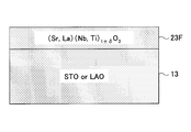
- Sectional drawing which shows the STO thin film doped with La and Nb used as the thermoelectric conversion element by 1st Embodiment. It is a flowchart which shows the manufacturing process of the STO thin film by 1st Embodiment. It is a graph showing the relationship between electrical conductivity and total dope amount about the STO thin film of FIG. 3 is a transmission electron microscope image of the STO thin film of FIG. 2 viewed from a direction perpendicular to the film surface. It is a transmission electron microscope image which shows the film
- FIG. 7 It is a figure explaining the measurement of the thermal conductivity by 3omega method. It is a graph explaining the measurement of the heat conductivity by 3omega method. It is a figure explaining the experiment which confirms the uniformity of the STO thin film of FIG.
- FIG. 7 it is a figure which shows the composition profile along line Line1.
- FIG. 7 it is a figure which shows the composition profile along line Line2.
- FIG. 7 it is a figure which overlaps and shows the profile of Drawing 8A and Drawing 8B.
- 3 is a graph showing the relationship between oxygen heat treatment and carrier concentration of the STO thin film of FIG. It is a graph which shows the power factor of the thermoelectric conversion element of FIG. It is sectional drawing which shows the structure of the thermoelectric conversion element by 1st Embodiment. It is a top view which shows the structure of the thermoelectric conversion element by 2nd Embodiment.
- FIG. 12B is a cross-sectional view taken along line AA ′ in FIG. 12A.
- FIG. 1 is a diagram showing a configuration of a sputtering apparatus 10 used for forming an STO thin film in the first embodiment. Note that the formation of the STO thin film in the present embodiment is not limited to the sputtering method using the sputtering apparatus 10 of FIG. 1, but can be formed by other PVD methods, for example, a pulse laser deposition method.
- a sputtering apparatus 10 includes a vacuum vessel 11 into which a sputtering gas such as Ar is introduced from a sputtering gas introduction port 11B and is evacuated to a high vacuum at an exhaust port 11A.
- a target holding base 12A for holding a target 12 made of STO is provided.
- a substrate holder 13A for holding the substrate to be processed 13 is provided above the vacuum container 11 so that the substrate to be processed 13 faces the target 12.
- a high frequency power source 12B is connected to the target holding base 12A, and the high frequency power source 12B applies the high frequency to the target 12 via the target holding base 12A.
- Plasma is generated between the processing substrate 13 and the generated plasma collides with the target 12, whereby the components of the target 12 are sputtered from the target 12.
- the substrate holder 13A is grounded, and the components sputtered from the target 12 are deposited on the substrate 13 to be processed on the substrate holder 13A, and a desired STO thin film is formed on the substrate 13 to be processed.
- the metal pieces 12D of the metal element to be doped into the strontium titanate thin film are arranged on the target 12 at a predetermined ratio.
- the thin film can be doped with a desired metal element at a desired ratio.
- FIG. 2 is a schematic sectional view showing an STO thin film 23F used as a thermoelectric conversion element according to the first embodiment
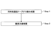
- FIG. 3 is a flowchart showing a manufacturing process of the STO thin film 23F in FIG.
- the STO thin film 23F is a film having a non-stoichiometric composition or a stoichiometric composition having oxygen deficiency, and has a film thickness in the range of 1 nm to 10 ⁇ m, preferably in the range of 10 nm to 1000 nm.
- the A seat is doped with Sr and the B seat is simultaneously doped with Nb at a high concentration, and the composition represented by the general formula (Sr, La) (Nb, Ti) 1 ⁇ ⁇ O 3 is obtained.
- the general formula (Sr, La) (Nb, Ti) 1 ⁇ ⁇ O 3 is obtained.
- the A and B seats of the STO thin film 23F are the ratio of the total number of atoms of Sr and Nb to the total of the A and B seats expressed by (La + Nb) / (Sr + La + Ti + Nb), and therefore the atomic concentration is 20% or more.
- Step 1 the sputtering apparatus 10 of FIG. 1 is formed on a suitable substrate, for example, a single crystal substrate 13 of strontium titanate or lanthanum aluminate (LaAlO 3 ). Is used to epitaxially form the STO thin film 23F highly doped with La and Nb.
- a suitable substrate for example, a single crystal substrate 13 of strontium titanate or lanthanum aluminate (LaAlO 3 ).
- the STO thin film 23F obtained in this way is heat-treated in an oxygen atmosphere in Step 2 to control the oxygen deficiency concentration in the STO thin film 23F.
- the carrier concentration in the film increases, the resistivity ⁇ in the equation (1) is reduced, and the electrical conductivity ⁇ is increased. Can do.
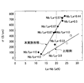
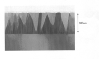
- FIG. 4 shows the hole mobility of electrons and the atoms occupying the B seat in the STO thin film 23F doped with La and Nb thus formed on the STO single crystal substrate 13 with a film thickness of 300 nm.
- the relationship with the atomic ratio (B / (A + B)) for the entire A seat and B seat is shown.
- the vertical axis represents the hole mobility of electrons
- the horizontal axis represents the atomic ratio of atoms occupying the B seat to the entire A seat and B seat (B / (A + B)), and accordingly ((La + Nb) / (Sr + La + Ti + Nb)).
- the atomic ratio is shown.
- the numerical value given to each point in FIG. 3 indicates the atomic ratio Nb / La between Nb and La.
- the electrical conductivity ⁇ of the STO thin film 23F increases as the total atomic concentration of Nb and La defined above increases, which is caused by doping. This reflects the situation where the carrier concentration in the thin film is increasing. In particular, when the total atomic concentration is increased beyond 20%, the electrical conductivity ⁇ of the STO thin film 23F exceeds 700 S / cm and approaches 800 S / cm.
- FIG. 4 shows a comparative example in which the STO thin film 23F is not doped with La but is doped only with Nb. In this case, the electrical conductivity ⁇ of the STO thin film is reduced to less than half.
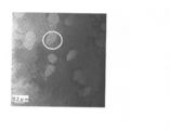
- 5A and 5B show transmission electron micrographs of the thin film obtained when the STO thin film 23F of FIG. 2 is doped with La and Ni at a concentration exceeding 20 atomic% at the same time. It is a figure shown about a film cross section.
- the STO film 23F doped in such a high concentration is a single crystal film, but is shown in white in a (001) plane orientation matrix shown in black in the film. It can be seen that many (031) plane orientation regions or domains are generated. As can be seen from FIG. 5A, the size of the generated domain of the (031) plane orientation is 0.2 ⁇ m, and it is considered that dislocations are formed at the boundary with the matrix.
- FIGS. 5A and 5B actually use a LaAlO 3 (LAO) substrate as the substrate 13 as described later in Example 1, and the STO thin film 23F has a concentration of 13.02 atomic% with La. Further, Nb is co-doped at a concentration of 8.4 atomic%, and RF magnetron sputtering is performed at a substrate temperature of 700 ° C. in a 1 Pa Ar gas atmosphere in the sputtering apparatus 10 of FIG. It was obtained by executing while supplying.
- LAO LaAlO 3
- the STO film 23F having a structure including such a domain it is considered that phonon scattering occurs due to dislocations existing at the domain boundary, and the thermal conductivity ⁇ in the film is greatly reduced. Therefore, there is a possibility that the figure of merit ZT can be greatly improved by using such an STO thin film 23F for a thermoelectric conversion element.
- FIG. 5C shows a comparative example, in which the STO thin film 23F of FIG. 2 is doped with Nb to a concentration of 14 atomic%, but in this case, no remarkable domain structure is observed.
- the domain structure of FIGS. 5A and 5B appears when the total dopant concentration exceeds 20%. ing.
- a similar domain structure appears when the dopant concentration exceeds 25%.
- the carrier concentration in the film is lowered as described above, but such a domain structure can be formed, and such a case is also included in this embodiment.
- 5A and 5B are prepared by arranging nine La pieces and Nb pieces as the metal pieces 12D on the target 12 in the sputtering apparatus 10 of FIG. 1, and the Nb in the thin film 23F is produced.
- the concentration is confirmed by inductively coupled plasma (ICP) spectroscopy.
- 5C is produced by arranging three Nb pieces as the metal piece 12D on the target 12 in the sputtering apparatus 10 shown in FIG. 1.
- the Nb concentration in the thin film 23F is determined by inductively coupled plasma. (ICP) Confirmed by spectroscopy.
- the thermal conductivity was measured by the 3 ⁇ method for the structure in which such a domain occurs.
- Non-patent documents 1 and 2 explain the principle and application examples of the 3 ⁇ method.
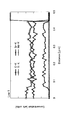
- FIG. 6A is a diagram showing an outline of measurement
- FIG. 6B is a graph showing measurement data.
- a thin silicon oxide film (not shown) is formed on the STO thin film 23F of FIG. 2 by sputtering for insulation, and a Cr / Au laminated structure is formed thereon. Measurement was performed by forming a line-shaped heater 23H from a conductive film, supplying alternating current having a frequency ⁇ from both terminals 23A and 23B to the heater 23H, and periodically heating the heater 23H.
- the heater 23H is also used as a temperature measuring device. Such temperature oscillation ⁇ T is caused by the diffusion of heat from the heater 23H that is periodically heated along the sample surface, and includes information on the thermal conductivity ⁇ of the sample.
- lines L 1R and L 1I show the relationship between the temperature oscillation ⁇ T and the logarithm of the heating frequency ⁇ thus obtained for the sample of FIG.
- the line L 1R represents the real part of the temperature oscillation ⁇ T that is in phase with the heating cycle, and forms a straight line with respect to the logarithm of the heating frequency ⁇ .
- the line L 1I represents the imaginary part of the temperature oscillation ⁇ T that is in opposite phase to the heating cycle, and is constant with respect to the heating frequency ⁇ .
- lines RL 1R and RL 1I are obtained when the electrode of FIG. 6A is formed directly on the STO substrate 13 without forming the STO thin film 23F in the sample of FIG. It is a line which shows the relationship between the temperature vibration (DELTA) T of the said STO board
- the line RL 1R represents the real part of the temperature oscillation ⁇ T that is in phase with the heating cycle and is linear with the logarithm of the heating frequency ⁇ .
- the line RL 1I represents the imaginary part of the temperature oscillation ⁇ T that is in opposite phase to the heating cycle, and is constant with respect to the heating frequency ⁇ .
- the thermal conductivity ⁇ of the STO substrate 13 (Sub) is calculated as 11.2 W / mK based on the slope of the line RL 1R , which is known as the thermal conductivity of the STO bulk single crystal. Matches the value of.
- the line L 1R is parallel to the line RL 1R and is shifted upward by about 0.7K.
- This shift amount ⁇ T film corresponds to the contribution of the thermal conductivity ⁇ of the STO thin film 23F.
- this shift amount ⁇ T film is independent of the heating frequency ⁇ , this corresponds to the situation in which the diffusion of heat in the surface direction of the sample can be ignored because the thin film 23F is thin.
- the STO thin film 23F according to the present embodiment includes the domain structure described above with reference to FIGS. 5A and 5B, phonon scattering is promoted in the film, and the thermal conductivity ⁇ is conventional, that is, non-patent literature. This is considered to be further reduced as compared with the STO thin film No. 3.
- Example 1 an LAO substrate is used as the substrate 13, and an (001) -oriented STO thin film 23F on which La and Nb are simultaneously doped is formed by the sputtering apparatus 10 of FIG.
- the substrate is formed at a substrate temperature of 700 ° C. by RF sputtering while supplying high-frequency power of 75 W under a reduced-pressure Ar atmosphere.
- the STO thin film 23F is doped with 13.2 atomic% La, 8.4 atomic% Nb, and oxygen vacancies at a rate of 16.2% per unit cell without performing heat treatment after film formation. .
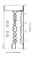
- FIG. 8B is a transmission electron microscope image of the film 23F viewed from the direction perpendicular to the film surface
- FIG. 8A is a composition profile along the straight line 1 in FIG. 7
- FIG. 8B is a composition along the straight line 2 in FIG.
- FIG. 8C is a view obtained by superimposing FIG. 8A and FIG. 8B.
- the straight line 1 and the straight line 2 are about 0.2 ⁇ m apart as shown in FIG.
- Example 2 the sample of Example 1 was further heat-treated in an oxygen atmosphere to optimize the power factor PF.
- FIG. 9 is a graph showing the relationship between the electron concentration n H obtained by the Hall effect in the STO thin film 23F according to Example 2 and the heat treatment temperature.
- the vertical axis indicates the electron concentration n H and the horizontal axis indicates the heat treatment temperature.
- the heat treatment is performed in an oxygen atmosphere of 1 atm for 2 hours.
- the electron concentration n H in the film is 10 20 cm ⁇ 3 to 10 ⁇ 10. It can be seen that it is possible to adjust to a range of 22 cm ⁇ 3 .
- the power factor PF S 2 qn ⁇ increases as described at the beginning.
- FIG. 9 shows that heat treatment in an oxygen atmosphere at a relatively low temperature of 20 ° C. to 600 ° C. effectively compensates for oxygen vacancies that trap and cancel carriers in the STO thin film 23F. Yes.
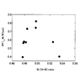
- FIG. 10 is a graph showing the power factor PF when a thermoelectric conversion element described later is manufactured using the STO thin film 23F of this example.
- the vertical axis represents the power factor PF
- the horizontal axis represents the ratio of the B seat element to the total (A + B) of the A seat and B seat of the perovskite structure, that is, B / (A + B).
- the power factor PF is maximized by selecting the ratio B / (A + B) in the vicinity of 0.50 in the STO film 23F having the electron concentration n H optimized as described above. I understand. This is because the total number of atoms of Sr and La occupying the A seat and the total number of Ti and Nb occupying the B seat are balanced, and the trapping or canceling of carriers by vacancies in the A seat or B seat is minimized. This corresponds to the situation where the concentration of carriers emitted by doping La, Nb, that is, electrons, is maximized.
- thermoelectric conversion element 20 Refer to FIG. 1
- the thermoelectric conversion element 20 includes the single crystal STO substrate 13, the STO thin film 23F epitaxially formed on the STO substrate 13, and first and second end portions on the STO thin film 23F.
- the first electrodes 22A and 22B made of an oxidation-resistant metal such as Pt and having a thickness of 100 nm, for example, and between the first end and the second end on the STO thin film 23F And the second electrode 24 formed in the region.
- thermoelectric conversion element 20 of FIG. 11 for example, the bottom surface of the substrate 13 is heated in a region near the first end and the second end, and the STO thin film 23F is cooled in the intermediate region. Or by cooling the bottom surface of the substrate 13 in the regions near the first end and the second end and heating the STO thin film 23F in the intermediate region, An output voltage due to the Seebeck effect is obtained between the output terminal OUT1 connected to 22B and the output terminal OUT2 connected to the second electrode 24.
- thermoelectric conversion element 20 of FIG. 11 a single crystal MgO substrate or a LaAlO 3 substrate can be used instead of the single crystal STO substrate 13.
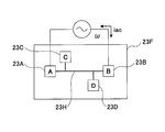
- FIG. 12A and 12B are a cross-sectional view and a plan view showing the configuration of the thermoelectric conversion device 40 according to the second embodiment, respectively.
- FIG. 12A shows a cross section along line AA ′ in the plan view of FIG. 12B.
- the thermoelectric conversion device 40 includes the single crystal STO substrate 13 and an STO thin film pattern formed on the substrate 13 and having the same structure as the STO thin film 23F of FIGS. 5A and 5B.
- 23F 1 , 23F 2 , 23F 3 , 23F 4 the STO thin film pattern 23F 1 has electrodes 22A and 22B at both ends thereof and electrodes 24 at the intermediate portion thereof. The same applies to the other STO thin film patterns 23F 2 , 23F 3 , and 23F 4 .
- STO thin film pattern - STO thin film pattern electrodes 22A and 22B on the emission 23F 1 adjacent connected in parallel - a first wiring W 1 to be connected to the electrode 24 on the emission 23F 2 is also the STO thin film pattern - STO thin film pattern electrodes 22A and 22B on the emission 23F 2 adjacent connected in parallel - a second wiring connected to the electrode 24 on the emission 23F 3 W 2 further wherein STO thin film pattern - down 23F STO thin film pattern electrodes 22A and 22B on 2 adjacent connected in parallel - the third wire W 3 to be connected to the electrode 24 on the emission 23F 3, further wherein the STO thin film pattern - electrode 22A on the emission 23F 4 and fourth wire W 4 which are connected in parallel 22B are formed.
- a heating / cooling device 41 having protrusions 41A, 41B, 41C, and 41D is shown with the protrusions 41A, 41B, 41C, and 41D surrounded by broken lines in FIG. 12A, respectively.
- the region 41a corresponds to the electrode 22A formed on the STO thin film 23f1
- the region 41b is the STO thin film 23F 1 electrode 22B formed on and the STO thin film 23F electrode 22A formed on the 2 corresponds to the region 41c corresponds to the STO thin film 23F 2 electrode 22B formed on and the STO thin film 23F 3 electrodes 22A formed on the area 41d is the STO thin film 23F 3 correspond to the formed electrode 22B and the STO thin film 23F 4 electrodes 22A formed on the upper
- the region 41e corresponds to the electrode 22B formed on the STO thin film 23F 4.
- a heating / cooling device 42 having projecting portions 42A, 42B, 42C, and 42D, and the projecting portions 42A, 42B, 42C, and 42D are shown by broken lines in FIG. 12A.
- the STO thin film 23F 1 area 42a enclosed by a also in the region 42b of the STO thin film 23F 2, also in the area 41c of the STO thin film 23F 3, also in the region 41d of the STO thin film 23F 4, provided in contact respectively
- the STO thin films 23F 1 to 23F 4 are cooled or heated in the regions 42a to 42e.
- the region 42a corresponds to the electrode 24 formed on the STO thin film 23F 1, wherein the region 41b corresponds to electrode 24 formed on the STO thin film 23F 2, the region 41c is the STO correspond to the electrodes 24 formed on the thin film 23F3, the area 41d corresponds to electrode 24 formed on the STO thin film 23F 4.
- the heating and cooling device 42 a central portion of the STO thin film 23F 1 ⁇ 23F 4 is cooled when the heating and cooling apparatus 4 1 heats the both end portions of the STO thin film 23F 1 ⁇ 23F 4 through the substrate 13
- the heating / cooling device 41 cools both ends of the STO thin films 23F1 to 23F4 via the substrate 13
- the central portions of the STO thin films 23F 1 to 23F 4 are heated, and the respective STO thin films 23F 1 to 23F 1 to in 23F 4 induces a temperature gradient in the lateral direction.
- thermoelectric conversion element is formed by the STO thin film that swings the domain structure.
- the thermoelectric conversion element using another perovskite film for example, a BaTiO 3 film
- the high concentration doping is performed.
- a similar domain structure can be generated in the perovskite film, and the thermal conductivity ⁇ can be reduced.
Abstract
熱電変換素子は、基板と、前記基板上に形成され、ペロブスカイト構造の化合物よりなる薄膜と、前記基板上に設けられ、前記薄膜の上面に第1の領域においてコンタクトする第1の電極と、前記薄膜の上面に前記第1の領域から離間した第2の領域においてコンタクトする第2の電極と、前記薄膜を、前記第1の領域において加熱または冷却する第1の加熱または冷却部と、前記薄膜を、前記第2の領域において加熱または冷却する第2の加熱または冷却部と、を含み、前記第2の加熱または冷却部は、前記第1の加熱または冷却部が前記薄膜の前記第2の領域を加熱する場合に前記薄膜の前記第1の領域を冷却し、前記第2の加熱または冷却部は前記第1の加熱または冷却部が前記薄膜の前記第1の領域を冷却する場合に前記薄膜の前記第2の領域を加熱し、前記薄膜中には、前記ペロブスカイト構造の化合物を構成する結晶中に、前記結晶とは異なる結晶方位の領域が形成されている。
Description
以下に説明する実施形態は、熱電変換素子およびその製造方法に関する。
現在、工場や発電所、さらには自動車などの輸送機関やコンピュータなどの情報処理装置においては、エネルギは消費された後、環境中に、廃熱の形で放出されている。そこで、このような廃熱を回収してこれをエネルギに変換できる熱変換素子が注目されている。
ゼーベック効果を使った熱電変換素子は、従来の熱電変換システムのような作動流体や複雑な駆動機構を必要とせず、様々なシステムからの廃熱を回収して電力に変換することができる。
特にチタン酸ストロンチウム(以下、STOと略記する)は、従来強誘電体素子への応用の面から研究されて来たが、従来の熱電変換素子のように有毒でかつ埋蔵量の少ないテルルやビスマスなどの材料を含んでおらず、また300Kにおいて0.8mVK-1に達する大きなゼーベック係数Sを与え、S2σで定義されるパワーファクタ(PF=S2σ)で30~40μW/cm・K2の大きな値を実現できることから、熱電変換素子の材料としても注目されている。ただしσは熱電変換素子の電気伝導度である。なおパワーファクタPFは、S2qnμでも表すことができる(PF=S2σ=S2qnμ)。ここでnは単位体積当たりのキャリア濃度、qはキャリア電荷、μはキャリアの移動度である。
このようにSTOの系では、パワーファクタPFは35μW/cmK2~40μW/cmK2の値に達するが、熱伝導率κがバルク結晶の場合で11W/mKと大きな値を有しているため、

このようなSTOよりなる熱電変換素子において大きな性能指数ZTを得ようとすると、STOに高い導電性をもたせると同時に、その熱伝導率κを低減する必要がある。
特開2010-161213号公報
Cahill, D. Rev. Sci. Instrum. 61(2), February 1990, pp802-808
Cahill, D., et al. Phys. Rev. B Vol.50, Number 9, 6077-6081 (1994)
Ravichandran, J., et al., Phys. Rev. B 82, 165126 (2010)
一の側面によれば熱電変換素子は、基板と、前記基板上に形成され、ペロブスカイト構造の化合物よりなる薄膜と、前記基板上に設けられ、前記薄膜の上面に第1の領域においてコンタクトする第1の電極と、前記薄膜の上面に前記第1の領域から離間した第2の領域においてコンタクトする第2の電極と、前記薄膜を、前記第1の領域において加熱または冷却する第1の加熱または冷却部と、前記薄膜を、前記第2の領域において加熱または冷却する第2の加熱または冷却部と、を含み、前記第2の加熱または冷却部は、前記第1の加熱または冷却部が前記薄膜の前記第2の領域を加熱する場合に前記薄膜の前記第1の領域を冷却し、前記第2の加熱または冷却部は前記第1の加熱または冷却部が前記薄膜の前記第1の領域を冷却する場合に前記薄膜の前記第2の領域を加熱し、前記薄膜中には、前記ペロブスカイト構造の化合物を構成する結晶中に、前記結晶とは異なる結晶方位の領域が形成されている。
本実施形態によれば、ペロブスカイト薄膜中にマトリクスとは結晶方位の異なる複数のドメインが形成されているため、ドメイン境界の転位によりフォノンの散乱が誘起される。その結果、ペロブスカイト薄膜の熱伝導率が減少し、熱電変換素子の性能指数ZTが向上する。
10 スパッタ装置
11 真空容器
11A 排気ポート
11B プラズマガス導入ポート
12 ターゲット
12A ターゲット保持台
12B 高周波電源
12D ドーパント金属片
13 被処理基板
13A 基板保持台
22,22A.22B 第1電極
23F La,NbドープSTO薄膜
23F1,23F2,23F3,23F4 La,NbドープSTO薄膜パタ―ン
24 第2電極
41,42 加熱/冷却部
41A~41D,42A~42D 突起
11 真空容器
11A 排気ポート
11B プラズマガス導入ポート
12 ターゲット
12A ターゲット保持台
12B 高周波電源
12D ドーパント金属片
13 被処理基板
13A 基板保持台
22,22A.22B 第1電極
23F La,NbドープSTO薄膜
23F1,23F2,23F3,23F4 La,NbドープSTO薄膜パタ―ン
24 第2電極
41,42 加熱/冷却部
41A~41D,42A~42D 突起
[第1の実施形態]
図1は、第1の実施形態においてSTO薄膜を形成するのに使われるスパッタ装置10の構成を示す図である。なお本実施形態におけるSTO薄膜の形成は、図1のスパッタ装置10を使ったスパッタ法に限定されるものではなく、他のPVD法、例えばパルスレーザ堆積法などにより形成することも可能である。
図1は、第1の実施形態においてSTO薄膜を形成するのに使われるスパッタ装置10の構成を示す図である。なお本実施形態におけるSTO薄膜の形成は、図1のスパッタ装置10を使ったスパッタ法に限定されるものではなく、他のPVD法、例えばパルスレーザ堆積法などにより形成することも可能である。
図1を参照するに、スパッタ装置10はスパッタガス導入ポート11BからArなどのスパッタガスを導入され排気ポート11Aにおいて高真空に排気される真空容器11を有し、前記真空容器11の下方には、STOよりなるターゲット12を保持するターゲット保持台12Aが設けられている。また前記真空容器11の上方には、被処理基板13を保持する基板保持台13Aが、前記被処理基板13が前記ターゲット12に対面するように設けられている。
前記ターゲット保持台12Aには高周波電源12Bが接続され、前記高周波電源12Bから前記ターゲット12に前記ターゲット保持台12Aを介して前記高周波を印加することにより、前記真空容器11中に前記ターゲット12と被処理基板13との間でプラズマが発生し、発生したプラズマが前記ターゲット12に衝突することにより、前記ターゲット12から、前記ターゲット12の成分がスパッタされる。
さらに前記基板保持台13Aは接地されており、前記ターゲット12からスパッタされた成分が前記基板保持台13A上の被処理基板13に堆積し、前記被処理基板13上に所望のSTO薄膜が形成される。
その際、図1のスパッタ装置10では、前記ターゲット12上にチタン酸ストロンチウム薄膜にドープしたい金属元素の金属片12Dが所定の割合で配置されており、これにより、前記被処理基板13上のSTO薄膜を所望の金属元素により、所望の割合でドープすることが可能となる。
図2は、第1の実施形態による、熱電変換素子として使われるSTO薄膜23Fを示す概略的断面図、図3は、前記図2のSTO薄膜23Fの製造工程を示すフローチャートである。
図2を参照するに、前記STO薄膜23Fは酸素欠損を有する非化学量論組成あるいは化学量論組成を有する膜であり、1nm~10μmの範囲、好ましくは10nm~1000nmの範囲の膜厚を有し、ペロブスカイト構造のA席がSrにより、またB席がNbにより同時に、高濃度にドープされており、一般式(Sr,La)(Nb,Ti)1±δO3で表される組成を有している。
一例では、前記STO薄膜23FのA席およびB席は、(La+Nb)/(Sr+La+Ti+Nb)で表したA席およびB席の合計に対するSrとNb合計の原子数の割合、従って原子濃度が20%以上、好ましくは24%以上になるように、それぞれSrおよびNbによりドープされている。このような高濃度ドープの効果については、後ほど詳細に説明する。
次に図3のフローチャートを参照するに、本実施形態ではまずステップ1において適当な基板、例えばチタン酸ストロンチウムあるいはランタンアルミネート(LaAlO3)の単結晶基板13上に、前記図1のスパッタ装置10を使って、LaおよびNbにより高濃度にドープされたSTO薄膜23Fをエピタキシャルに形成する。
次にこのようにして得られたSTO薄膜23Fをステップ2において酸素雰囲気中において熱処理し、前記STO薄膜23F中の酸素欠損濃度を制御する。このように前記STO薄膜23F中の酸素欠損濃度を所定値に制御することで膜中のキャリア濃度が増大し、前記式(1)における抵抗率ρを低減し、電気伝導度σを増大させることができる。
図4は、このようにしてSTO単結晶基板13上に300nmの膜厚で形成されたLaとNbをドープしたSTO薄膜23Fにおいて、電子のホール(Hall)移動度と、B席を占有する原子のA席およびB席の全体に対する原子比(B/(A+B))との関係を示している。ここで縦軸は電子のホール移動度、横軸は、B席を占有する原子のA席およびB席の全体に対する原子比(B/(A+B))、従って((La+Nb)/(Sr+La+Ti+Nb))の原子比を示したものである。図3において各点に付した数値は、NbとLaの原子比Nb/Laを示している。
図4を参照するに、本実施形態によれば、前記STO薄膜23Fの電気伝導度σは、上に定義したNbとLaの合計の原子濃度を増大させるにつれて増大しており、これはドーピングにより薄膜中におけるキャリア濃度が増大している状況を反映している。特に合計の原子濃度を、20%を超えて増大させた場合、前記STO薄膜23Fの電気伝導度σは700S/cmを超え、800S/cmに近づくことがわかる。
図4には、前記STO薄膜23FにおいてLaのドープを行わず、Nbのドープのみを行った比較対照例を示すが、この場合には、STO薄膜の電気伝導度σが半分以下に低減しているのがわかる。これはB席のみにドープを行った結果、ABO3で表されるペロブスカイト型化合物の化学量論組成に対しA席とB席の間で原子数の均衡が崩れて欠陥が発生し、かかる欠陥によりキャリアが相殺されていることを示唆している。
図4には、前記STO薄膜23FにおいてLaのドープを行わず、Nbのドープのみを行った比較対照例を示すが、この場合には、STO薄膜の電気伝導度σが半分以下に低減しているのがわかる。これはB席のみにドープを行った結果、ABO3で表されるペロブスカイト型化合物の化学量論組成に対しA席とB席の間で原子数の均衡が崩れて欠陥が発生し、かかる欠陥によりキャリアが相殺されていることを示唆している。
図5Aおよび図5Bは、前記図2のSTO薄膜23Fにおいて、LaおよびNiを同時に合計で20原子%を超える濃度でドープを行った場合に得られた薄膜の透過電子顕微鏡写真を、それぞれ膜上面および膜断面について示す図である。
図5Aおよび図5Bを参照するに、このように高濃度でドープしたSTO膜23Fは、単結晶膜ではあるものの、膜中に黒く示された(001)面方位のマトリクス中に、白く示された(031)面方位の領域あるいはドメインが多数発生しているのがわかる。発生した(031)面方位のドメインの大きさは、図5Aからわかるように0.2μmにもおよび、マトリクスとの境界には転位が形成されているものと考えられる。
図5A,図5Bの試料は、実際には後で実施例1において説明するように、前記基板13としてLaAlO3(LAO)基板を使い、前記STO薄膜23FをLaにより13.02原子%の濃度で、またNbにより、8.4原子%の濃度で同時ドープしたものであり、前記図1のスパッタ装置10において1PaのArガス雰囲気中、RFマグネトロンスパッタリングを700℃の基板温度において、75Wのパワーを供給しながら実行することにより得られたものである。
このようなドメインを含む構造のSTO膜23Fでは、ドメイン境界に存在する転位によりフォノンの散乱が生じ、膜中における熱伝導率κが大きく低減されると考えられる。そこでこのようなSTO薄膜23Fを熱電変換素子に使うことにより、性能指数ZTを大きく向上できる可能性がある。
これに対し図5Cは比較対照例を示し、前記図2のSTO薄膜23FをNbのみにより14原子%の濃度にドープしているが、この場合には、顕著なドメイン構造は見られない。先にも述べたようにSTO薄膜23FにおいてLaおよびNbを同時にドーピングした場合には、合計のドーパント濃度が20%を超えたあたりから、図5A,図5Bのドメイン構造が出現することが確認されている。一方、Nbのみをドープした場合には、同様なドメイン構造は、ドーパント濃度が25%を超えた当たりから出現する。Nbのみを高濃度でドープした場合には、先にも説明したように膜中のキャリア濃度が低下するが、このようなドメイン構造を形成できるため、このような場合も本実施形態に含めることにする。
なお前記図5Aおよび図5Bの試料は、前記図1のスパッタ装置10において前記ターゲット12上に前記金属片12DとしてLa片とNb片を9個配置して作製しており、薄膜23F中のNb濃度は誘導結合プラズマ(ICP)スペクトロスコピにより確認している。また図5Cの試料では、前記図1のスパッタ装置10において前記ターゲット12上に前記金属片12DとしてNb片を3個配置して作製しており、同様に薄膜23F中のNb濃度は誘導結合プラズマ(ICP)スペクトロスコピにより確認している。
先にも述べたように、図5A,図5Bのような、マトリクス中に多数の結晶方位の異なるドメインを含むSTO膜では、ドメイン境界を構成する転位によりフォノンが散乱され、熱伝導率κが大きく低減されることが予期される。このような熱伝導率κの低減は、先に式(1)で説明した性能指数ZTを増大させるように作用する。
そこで本実施形態では、このようなドメインが生じている構造に対し、3ω法により、熱伝導率の測定を行った。3ω法の原理および応用例は、非特許文献1,2に解説されている。
図6Aは測定の概要を示す図、図6Bは測定データを示すグラフである。
図6Aを参照するに、本実施形態では、絶縁のため前記図2のSTO薄膜23F上に薄いシリコン酸化膜(図示せず)をスパッタ法などにより形成し、その上にCr/Au積層構造の導電膜によりライン状のヒータ23Hを形成し、前記ヒータ23Hに、両端の端子23A,23Bから周波数がωの交流を供給し、前記ヒータ23Hを周期的に加熱することにより測定を行った。
このように前記ヒータ23Hに周波数がωの交流を供給することにより、試料は2ωの周波数で繰り返し加熱される。そこで、前記ヒータ23Hの抵抗値を、前記交流に位相がロックされた周波数が3ωの電圧を、前記端子23Aと23Bの間において端子23Cと23Dの間に印加することにより測定し、前記測定された抵抗値をもとに前記試料の温度振動(temperature oscillation)ΔTを、各周波数について求める。ここでは前記ヒータ23Hは温度測定器としても使われている。このような温度振動ΔTは、周期的に加熱される前記ヒータ23Hからの熱が試料面に沿って拡散することにより生じるもので、試料の熱伝導率κに関する情報を含んでいる。
図6B中、線L1RおよびL1Iは、このようにして図2の試料について得た、温度振動ΔTと加熱周波数ωの対数との間の関係を示す。ただし線L1Rは加熱サイクルに同相となる温度振動ΔTの実数部を表し、加熱周波数ωの対数に対して直線をなす。一方線L1Iは加熱サイクルに逆相となる温度振動ΔTの虚数部を表し、加熱周波数ωに対して一定となる。
さらに図6B中、線RL1RおよびRL1Iは、このようにして前記図2の試料おいて、STO薄膜23Fを形成せず、STO基板13上に直接に図6Aの電極を形成した場合の、前記STO基板13の温度振動ΔTと加熱周波数ωの対数との間の関係を示す線である。ここでも線RL1Rは加熱サイクルに同相となる温度振動ΔTの実数部を表し、加熱周波数ωの対数に対して直線をなす。一方線RL1Iは加熱サイクルに逆相となる温度振動ΔTの虚数部を表し、加熱周波数ωに対して一定となる。
図6B中、前記線RL1Rの傾きに基づいて、前記STO基板13(Sub)の熱伝導率κが11.2W/mKと計算されるが、これはSTOバルク単結晶の熱伝導率として公知の値と一致している。
これに対し図2に示す、STO基板13上にSTO薄膜23Fを形成した試料(Sub+film)では、線L1Rは前記線RL1Rと平行で、0.7Kほど上方にシフトしており、このシフト量ΔTfilmが前記STO薄膜23Fの熱伝導率κの寄与に対応する。このシフト量ΔTfilmは前記加熱周波数ωに対して独立であるが、これは前記薄膜23Fが薄いため、試料の面方向への熱の拡散が無視できる事情に対応している。
前記シフト量ΔTfilmから熱伝導率κを1次元熱伝導方程式より求めると、熱伝導率κとして2W/mKの値が得られる。この値は、STOバルク単結晶の熱伝導率(κbulk)よりもはるかに小さく、またSTO薄膜について従来報告されている4W/mK~5W/mKの値(非特許文献3)の半分以下になっている。
すなわち本実施形態によるSTO薄膜23Fは、先に図5A,図5Bで説明したドメイン構造を含んでいるため、膜中においてフォノンの散乱が促進され、熱伝導率κが従来の、すなわち非特許文献3のSTO薄膜に比べ、さらに低減されるものと考えられる。
以下、実施例を説明する。
実施例1では、先にも述べたように前記基板13としてLAO基板を使い、その上にLaとNbを同時ドープした(001)面方位のSTO薄膜23Fを前記図1のスパッタ装置10により、RFスパッタ法により、減圧Ar雰囲気下、75Wの高周波電力を供給しながら700℃の基板温度で形成している。
成膜後の熱処理を行わない状態で、前記STO薄膜23FはLaを13.2原子%、Nbを8.4原子%、酸素空孔を単位胞あたり16.2%の割合でドープされている。
先に図5A,図5Bで説明した通り、前記STO薄膜23F中には(001)面方位のペロブスカイトマトリクス中に多数の(031)面方位のドメインが島状に形成されており、図6A,図6Bで説明した通り、前記STO薄膜23Fの熱伝導率κは2W/mKにまで減少しているのが確認された。
なお、このようにして得られたSTO膜23Fについて、図7に示す直線Line1およびLine2に沿って、膜中のC(炭素)、Sr,TiおよびNbについて組成プロファイルを求めたところ、図8Aおよび図8Bに示す結果が得られた。ただし図7は膜23Fを膜面に対して垂直方向から見た透過電子顕微鏡像、図8Aは図7中、直線Line1に沿った組成プロファイル、図8Bは図7中、直線Line2に沿った組成プロファイルであり、図8Cは前記図8Aと図8Bを重ね合わせた図である。前記直線Line1および直線Line2は、図7に示すように約0.2μm離れている。
図8Aおよび図8Bを参照するに、前記STO膜23F中におけるSr,Ti,Nbの前記直線Line1および直線Line2に沿った分布はほぼ一様であることがわかる。また図8Cを参照するに、前記直線Line1に沿った分布と前記直線Line2に沿った分布とは重なっており、前記直線Line1,Line2に対して直角な方向においてもSr,Ti,Nbの分布は一様であることがわかる。
なお図7の透過電子顕微鏡像において、白く見える部分が前記図5Aにおける(031)面方位の領域に対応する。
実施例2では、先の実施例1の試料をさらに酸素雰囲気中で熱処理し、パワーファクタPFを最適化した。
図9は、実施例2によるSTO薄膜23F中におけるホール効果により求めた電子濃度nHと、熱処理温度の関係を示すグラフである。ただし図9中、縦軸は電子濃度nHを、横軸は熱処理温度を示す。
図9を参照するに、熱処理は1気圧の酸素雰囲気中にて2時間行っているが、600℃以下の温度で熱処理することにより、膜中の電子濃度nHを1020cm-3~1022cm-3の範囲に調整することが可能であるのがわかる。膜中の電子濃度nHが増大すると、冒頭に記載したようにPF=S2qnμで与えられるパワーファクタPFが増大する。図9は、20℃~600℃の比較的低温での酸素雰囲気中での熱処理により、STO薄膜23F中においてキャリアを捕獲したり相殺したりする酸素欠損が効果的に補償されることを示している。
図10は、本実施例のSTO薄膜23Fを使って、後で説明する熱電変換素子を作製した場合のパワーファクタPFを示すグラフである。ただし縦軸はパワーファクタPFを、横軸はペロブスカイト構造のA席およびB席の総計(A+B)に対するB席元素の割合、すなわちB/(A+B)を示す。
図10を参照するに、このように電子濃度nHを最適化したSTO膜23Fにおいて、前記比率B/(A+B)を0.50近傍に選ぶことにより、パワーファクタPFが最大になっているのがわかる。これは、A席を占有するSrおよびLaの総原子数とB席を占有するTiおよびNbの総原子数が平衡し、A席あるいはB席における空格子点によるキャリアの捕獲あるいは相殺が最小となり、LaおよびNbのドーピングにより放出されたキャリア、すなわち電子の濃度が最大になる事情に対応している。
先に図5A,図5Bで説明した(031)面方位のドメインは、前記STO薄膜23Fに対してこのような酸素雰囲気中での熱処理をした後でも、残留することが確認されている。
次に、本実施形態による熱電変換素子20について、図11を参照しながら説明する。
図11を参照するに、熱電変換素子20は前記単結晶STO基板13と、前記STO基板13上にエピタキシャルに形成されたSTO薄膜23Fと、前記STO薄膜23F上の第1および第2の端部近傍の領域にPtなどの耐酸化性金属よりなり例えば厚さが100nmの第1の電極22Aおよび22Bと、前記STO薄膜23F上の、前記第1の端部と前記第2の端部の中間の領域に形成された第2の電極24とより構成されている。
図11の熱電変換素子20では、例えば前記基板13の底面を、前記第1の端部および第2の端部近傍の領域において加熱し、前記STO薄膜23Fを、前記中間の領域において冷却することにより、あるいは前記基板13の底面を、前記第1の端部および第2の端部近傍の領域において冷却し前記STO薄膜23Fを前記中間の領域において加熱することにより、前記第1の電極22Aおよび22Bに接続された出力端子OUT1と前記第2の電極24に接続された出力端子OUT2との間にゼーベック効果による出力電圧が得られる。
なお図11の熱電変換素子20において、前記単結晶STO基板13に代えて、単結晶MgO基板やLaAlO3基板を使うことも可能である。
[第2の実施形態]
図12Aおよび図12Bは、それぞれ第2の実施形態による熱電変換装置40の構成を示す断面図および平面図を示す。ただし図12Aは図12Bの平面図中、線A-A'に沿った断面を示している。
図12Aおよび図12Bは、それぞれ第2の実施形態による熱電変換装置40の構成を示す断面図および平面図を示す。ただし図12Aは図12Bの平面図中、線A-A'に沿った断面を示している。
図12A,図12Bを参照するに、熱電変換装置40は前記単結晶STO基板13と、前記基板13上に形成され各々は図5A,図5BのSTO薄膜23Fと同じ構造を有するSTO薄膜パタ―ン23F1,23F2,23F3,23F4を含み、前記STO薄膜パタ―ン23F1はその両端部に電極22Aおよび22Bを、また中間部に電極24を有している。他のSTO薄膜パタ―ン23F2,23F3,23F4も同様である。
前記基板13上では前記STO薄膜パタ―ン23F1上の電極22Aおよび22Bを並列接続して隣接するSTO薄膜パタ―ン23F2上の電極24に接続する第1の配線W1が、また前記STO薄膜パタ―ン23F2上の電極22Aおよび22Bを並列接続して隣接するSTO薄膜パタ―ン23F3上の電極24に接続する第2の配線W2が、さらに前記STO薄膜パタ―ン23F2上の電極22Aおよび22Bを並列接続して隣接するSTO薄膜パタ―ン23F3上の電極24に接続する第3の配線W3が、さらに前記STO薄膜パタ―ン23F4上の電極22Aおよび22Bを並列接続する第4の配線W4が形成されている。
さらに前記基板13の下には、突起部41A,41B,41C,41Dを有する加熱/冷却装置41が、前記突起部41A、41B,41C,41Dを、それぞれ図12A中に破線で囲んで示す前記基板13のうちSTO薄膜23F1の領域41aに、またSTO薄膜23F1からSTO薄膜23F2にまたがる領域41bに、またSTO薄膜23F2からSTO薄膜23F3にまたがる領域41cに、またSTO薄膜23F3からSTO薄膜23F4にまたがる領域41dに、さらにSTO薄膜23F4の領域41eにコンタクトして設けられており、前記STO薄膜23F1~23F4を前記領域41a~41eにおいて加熱あるいは冷却する。前記領域41aは前記STO薄膜23F1上に形成された電極22Aに対応しており、前記領域41bは前記STO薄膜23F1上に形成された電極22Bおよび前記STO薄膜23F2上に形成された電極22Aに対応しており、前記領域41cは前記STO薄膜23F2上に形成された電極22Bおよび前記STO薄膜23F3上に形成された電極22Aに対応しており、前記領域41dは前記STO薄膜23F3上に形成された電極22Bおよび前記STO薄膜23F4上に形成された電極22Aに対応しており、前記領域41eは前記STO薄膜23F4上に形成された電極22Bに対応している。
また前記STO薄膜23F1~23F4の上方には、突起部42A,42B,42C,42Dを有する加熱/冷却装置42が、前記突起部42A,42B,42C,42Dを、それぞれ図12A中に破線で囲んで示す前記STO薄膜23F1の領域42aに、またSTO薄膜23F2の領域42bに、またSTO薄膜23F3の領域41cに、またSTO薄膜23F4の領域41dに、それぞれコンタクトして設けられており、前記STO薄膜23F1~23F4を前記領域42a~42eにおいて冷却あるいは加熱する。前記領域42aは前記STO薄膜23F1上に形成された電極24に対応しており、前記領域41bは前記STO薄膜23F2上に形成された電極24に対応しており、前記領域41cは前記STO薄膜23F3上に形成された電極24に対応しており、前記領域41dは前記STO薄膜23F4上に形成された電極24に対応している。
前記加熱冷却装置42は、前記加熱冷却装置41が前記基板13を介して前記STO薄膜23F1~23F4の両端部を加熱する場合に前記STO薄膜23F1~23F4の中央部を冷却し、また前記加熱冷却装置41が前記基板13を介して前記STO薄膜23F1~23F4の両端部を冷却する場合に前記STO薄膜23F1~23F4の中央部を加熱し、それぞれのSTO薄膜23F1~23F4中において、横方向の温度勾配を誘起する。さらに前記STO薄膜23F1の電極24に出力端子OUT1を接続し、STO薄膜23F4の電極22Aおよび22Bに出力端子OUT2を接続することにより、前記出力端子OUT1とOUT2の間に、各々図10の構成を有しSTO薄膜23F1~23F3のいずれかを有する熱電変換素子20を直列に接続したのと等価な出力電圧を得ることができる。
以上の各実施形態では、ドメイン構造を揺するSTO薄膜により熱電変換素子を形成していたが、他のペロブスカイト膜、例えばBaTiO3膜などを使った熱電変換素子においても、高濃度ドープをすることにより、ペロブスカイト膜中に同様なドメイン構造を発生させることができ、熱伝導率κを低減することができる。
以上、本発明を好ましい実施例について説明したが、本発明はかかる特定の実施例に限定されるものではなく、特許請求の範囲に記載した要旨内において様々な変形・変更が可能である。
Claims (10)
- 基板と、
前記基板上に形成され、ペロブスカイト構造の化合物よりなる薄膜と、
前記基板上に設けられ、前記薄膜の上面に第1の領域においてコンタクトする第1の電極と、
前記薄膜の上面に前記第1の領域から離間した第2の領域においてコンタクトする第2の電極と、
前記薄膜を、前記第1の領域において加熱または冷却する第1の加熱または冷却部と、
前記薄膜を、前記第2の領域において加熱または冷却する第2の加熱または冷却部と、
を含み、
前記第2の加熱または冷却部は、前記第1の加熱または冷却部が前記薄膜の前記第2の領域を加熱する場合に前記薄膜の前記第1の領域を冷却し、
前記第2の加熱または冷却部は前記第1の加熱または冷却部が前記薄膜の前記第1の領域を冷却する場合に前記薄膜の前記第2の領域を加熱し、
前記薄膜中には、前記ペロブスカイト構造の化合物を構成する結晶中に、前記結晶とは異なる結晶方位の領域が形成されている熱電変換素子。 - 前記薄膜は(001)面方位のSrTiO3の単結晶薄膜であり、前記複数の領域は、(031)面方位を有することを特徴とする請求項1記載の熱電変換素子。
- 前記薄膜はSrTiO3の単結晶薄膜であり、熱伝導率κが2W/mK以下であることを特徴とする請求項1記載の熱電変換素子。
- 前記薄膜は、少なくともLa(ランタン)とNb(ニオブ)を、合計で20原子%以上の割合で含むことを特徴とする請求項3記載の熱電変換素子。
- 前記Laは前記ペロブスカイト構造のA席に入り、前記Nbは前記ペロブスカイト構造のB席に入ることを特徴とする請求項4記載の熱電変換素子。
- 前記薄膜は、Nbを25原子%以上の割合で含むことを特徴とする請求項3記載の熱電変換素子。
- 前記薄膜は酸素欠損を含み、1020cm-3~1022cm-3の範囲のキャリア濃度を有していることを特徴とする請求項3記載の熱電変換素子。
- 基板上に形成され、ペロブスカイト構造の化合物よりなる薄膜を形成する工程と、
前記薄膜の上面に、第1の領域において第1の電極を形成する工程と、
前記薄膜の上面に、前記第1の領域から離間した第2の領域において第2の電極を形成する工程と、
前記第1の領域に加熱または冷却部を形成する工程と、
前記第2の領域に冷却または加熱部を形成する工程と、
を含み、
前記薄膜を形成する工程は、前記薄膜を構成する前記ペロブスカイト構造の化合物の結晶中に、前記結晶のマトリクスとは結晶方位の異なる領域が形成されるような濃度で、不純物元素をドープする工程を含むことを特徴とする熱電変換素子の製造方法。 - 前記ペロブスカイト構造の化合物は酸素欠損を含むチタン酸ストロンチウムであり、前記不純物元素はLa(ランタン)およびNb(ニオブ)であり、LaおよびNbは合計で20原子%以上の濃度でドープされることを特徴とする請求項8記載の熱電変換素子の製造方法。
- 前記ペロブスカイト構造の化合物は酸素欠損を含むチタン酸ストロンチウムであり、前記不純物元素はNb(ニオブ)であり、25原子%以上の濃度でドープされることを特徴とする請求項8記載の熱電変換素子の製造方法。
Priority Applications (3)
| Application Number | Priority Date | Filing Date | Title |
|---|---|---|---|
| PCT/JP2012/052283 WO2013114592A1 (ja) | 2012-02-01 | 2012-02-01 | 熱電変換素子およびその製造方法 |
| JP2013556145A JP6086071B2 (ja) | 2012-02-01 | 2012-02-01 | 熱電変換素子およびその製造方法 |
| US14/449,260 US9508912B2 (en) | 2012-02-01 | 2014-08-01 | Thermoelectric conversion device having perovskite crystal including grain domain |
Applications Claiming Priority (1)
| Application Number | Priority Date | Filing Date | Title |
|---|---|---|---|
| PCT/JP2012/052283 WO2013114592A1 (ja) | 2012-02-01 | 2012-02-01 | 熱電変換素子およびその製造方法 |
Related Child Applications (1)
| Application Number | Title | Priority Date | Filing Date |
|---|---|---|---|
| US14/449,260 Continuation US9508912B2 (en) | 2012-02-01 | 2014-08-01 | Thermoelectric conversion device having perovskite crystal including grain domain |
Publications (1)
| Publication Number | Publication Date |
|---|---|
| WO2013114592A1 true WO2013114592A1 (ja) | 2013-08-08 |
Family
ID=48904670
Family Applications (1)
| Application Number | Title | Priority Date | Filing Date |
|---|---|---|---|
| PCT/JP2012/052283 WO2013114592A1 (ja) | 2012-02-01 | 2012-02-01 | 熱電変換素子およびその製造方法 |
Country Status (3)
| Country | Link |
|---|---|
| US (1) | US9508912B2 (ja) |
| JP (1) | JP6086071B2 (ja) |
| WO (1) | WO2013114592A1 (ja) |
Cited By (3)
| Publication number | Priority date | Publication date | Assignee | Title |
|---|---|---|---|---|
| WO2016129082A1 (ja) * | 2015-02-12 | 2016-08-18 | 株式会社日立製作所 | 薄膜熱電変換モジュールおよびその製造方法 |
| JP2017504178A (ja) * | 2014-11-28 | 2017-02-02 | アールエフトロン カンパニー リミテッドRftron Co.,Ltd. | スズ金属ターゲットを利用したスズ酸化物層の形成方法 |
| JP7473112B2 (ja) | 2020-11-17 | 2024-04-23 | 国立大学法人東北大学 | 圧電体薄膜、圧電体薄膜の製造装置、圧電体薄膜の製造方法、および、疲労推定システム |
Citations (1)
| Publication number | Priority date | Publication date | Assignee | Title |
|---|---|---|---|---|
| WO2011065185A1 (ja) * | 2009-11-27 | 2011-06-03 | 富士通株式会社 | 熱電変換モジュール及びその製造方法 |
Family Cites Families (6)
| Publication number | Priority date | Publication date | Assignee | Title |
|---|---|---|---|---|
| JP3999300B2 (ja) * | 1997-02-07 | 2007-10-31 | Tdk株式会社 | 強誘電体薄膜およびその製造方法 |
| WO2008109564A1 (en) * | 2007-03-02 | 2008-09-12 | The Regents Of The University Of California | Complex oxides useful for thermoelectric energy conversion |
| JP5403497B2 (ja) * | 2007-09-05 | 2014-01-29 | 独立行政法人物質・材料研究機構 | 結晶成長用基板とこれを用いた結晶成長方法 |
| JP2010161213A (ja) | 2009-01-08 | 2010-07-22 | Tokuyama Corp | 熱電変換材料およびその製造方法 |
| JP2010165843A (ja) * | 2009-01-15 | 2010-07-29 | Sumitomo Chemical Co Ltd | 熱電変換モジュールの製造方法及び熱電変換モジュール |
| JP2011243824A (ja) * | 2010-05-20 | 2011-12-01 | Panasonic Corp | 異方的熱電材料とこれを用いた放射検出器および発電デバイス |
-
2012
- 2012-02-01 JP JP2013556145A patent/JP6086071B2/ja not_active Expired - Fee Related
- 2012-02-01 WO PCT/JP2012/052283 patent/WO2013114592A1/ja active Application Filing
-
2014
- 2014-08-01 US US14/449,260 patent/US9508912B2/en not_active Expired - Fee Related
Patent Citations (1)
| Publication number | Priority date | Publication date | Assignee | Title |
|---|---|---|---|---|
| WO2011065185A1 (ja) * | 2009-11-27 | 2011-06-03 | 富士通株式会社 | 熱電変換モジュール及びその製造方法 |
Non-Patent Citations (2)
| Title |
|---|
| J.D.BANIECKI ET AL.: "Composition-Thermoelectric Property Relationships of Sputter Deposited Epitaxial SrxLayTimNbnO3-5 Thin Films", DAI 58 KAI EXTENDED ABSTRACTS, 9 March 2011 (2011-03-09) * |
| SHINGO OHTA ET AL.: "Large thermoelectric performance of heavily Nb-doped SrTi03 epitaxial film at high temperature", APPLIED PHYSICS LETTERS, vol. 87, 2005, pages 092108 * |
Cited By (3)
| Publication number | Priority date | Publication date | Assignee | Title |
|---|---|---|---|---|
| JP2017504178A (ja) * | 2014-11-28 | 2017-02-02 | アールエフトロン カンパニー リミテッドRftron Co.,Ltd. | スズ金属ターゲットを利用したスズ酸化物層の形成方法 |
| WO2016129082A1 (ja) * | 2015-02-12 | 2016-08-18 | 株式会社日立製作所 | 薄膜熱電変換モジュールおよびその製造方法 |
| JP7473112B2 (ja) | 2020-11-17 | 2024-04-23 | 国立大学法人東北大学 | 圧電体薄膜、圧電体薄膜の製造装置、圧電体薄膜の製造方法、および、疲労推定システム |
Also Published As
| Publication number | Publication date |
|---|---|
| JPWO2013114592A1 (ja) | 2015-05-11 |
| US9508912B2 (en) | 2016-11-29 |
| US20140338717A1 (en) | 2014-11-20 |
| JP6086071B2 (ja) | 2017-03-01 |
Similar Documents
| Publication | Publication Date | Title |
|---|---|---|
| Abutaha et al. | Enhanced thermoelectric figure-of-merit in thermally robust, nanostructured superlattices based on SrTiO3 | |
| Zhang et al. | Growth of topological insulator Bi2Se3 thin films on SrTiO3 with large tunability in chemical potential | |
| Chen et al. | Influence of defects on structural and electrical properties of VO2 thin films | |
| US20190245130A1 (en) | Giant Cross-Plane Seebeck Effect in Oxide Metal Semiconductor Superlattices for Spin-Magnetic Thermoelectric Devices | |
| Quintela et al. | Epitaxial CrN thin films with high thermoelectric figure of merit | |
| Sarath Kumar et al. | Lattice dynamics and substrate-dependent transport properties of (In, Yb)-doped CoSb3 skutterudite thin films | |
| US9048380B2 (en) | Thermoelectric conversion material and production method for thermoelectric conversion material | |
| Wang et al. | Synthesis process and thermoelectric properties of n-type tin selenide thin films | |
| Hirai et al. | Semimetallic transport properties of epitaxially stabilized perovskite CaIrO3 films | |
| Orikasa et al. | Effects of oxygen gas pressure on structural, electrical, and thermoelectric properties of (ZnO) 3In2O3 thin films deposited by rf magnetron sputtering | |
| Singamaneni et al. | Ferroelectric and ferromagnetic properties in BaTiO3 thin films on Si (100) | |
| Sarath Kumar et al. | Effect of oxygen vacancy distribution on the thermoelectric properties of La-doped SrTiO3 epitaxial thin films | |
| JP5773072B2 (ja) | 熱電変換素子 | |
| Yan et al. | Phase transition and temperature stability of piezoelectric properties in Mn-modified Pb (Mg1/3Nb2/3) O3-PbZrO3-PbTiO3 ceramics | |
| Panwar et al. | Few layer graphene synthesized by filtered cathodic vacuum arc technique | |
| JP6086071B2 (ja) | 熱電変換素子およびその製造方法 | |
| Lee et al. | Thermal stability of giant thermoelectric Seebeck coefficient for SrTiO3/SrTi0. 8Nb0. 2O3 superlattices at 900 K | |
| US10886451B2 (en) | Thermoelectric material, method of fabricating the same, and thermoelectric device | |
| Bala et al. | Effect of thermal annealing on thermoelectric properties of BixSb2− xTe3 thin films grown by sputtering | |
| Ikeda et al. | Thermoelectric transport in the layered Ca3Co4–xRhxO9 single crystals | |
| JP2012186230A (ja) | 熱電変換素子および熱電変換材料 | |
| Shreiber et al. | Some unusual behavior of dielectric properties of SrTiO3 metal organic chemical vapor deposition grown thin films | |
| Sudheendran et al. | Microwave dielectric and Raman scattering studies on bismuth zinc niobate thin films | |
| TW202239981A (zh) | 磁性材料、積層體及積層體之製造方法、以及熱電轉換元件及磁性感應器 | |
| Li et al. | Effect of nanowires in microporous structures on the thermoelectric properties of oxidized Sb-doped ZnO film |
Legal Events
| Date | Code | Title | Description |
|---|---|---|---|
| 121 | Ep: the epo has been informed by wipo that ep was designated in this application |
Ref document number: 12867530 Country of ref document: EP Kind code of ref document: A1 |
|
| ENP | Entry into the national phase |
Ref document number: 2013556145 Country of ref document: JP Kind code of ref document: A |
|
| NENP | Non-entry into the national phase |
Ref country code: DE |
|
| 122 | Ep: pct application non-entry in european phase |
Ref document number: 12867530 Country of ref document: EP Kind code of ref document: A1 |