WO2013100674A1 - 승압형 dc-dc 컨버터 - Google Patents
승압형 dc-dc 컨버터 Download PDFInfo
- Publication number
- WO2013100674A1 WO2013100674A1 PCT/KR2012/011657 KR2012011657W WO2013100674A1 WO 2013100674 A1 WO2013100674 A1 WO 2013100674A1 KR 2012011657 W KR2012011657 W KR 2012011657W WO 2013100674 A1 WO2013100674 A1 WO 2013100674A1
- Authority
- WO
- WIPO (PCT)
- Prior art keywords
- switch
- transformer
- series
- diode
- converter
- Prior art date
- Legal status (The legal status is an assumption and is not a legal conclusion. Google has not performed a legal analysis and makes no representation as to the accuracy of the status listed.)
- Ceased
Links
Images


Classifications
-
- H—ELECTRICITY
- H02—GENERATION; CONVERSION OR DISTRIBUTION OF ELECTRIC POWER
- H02M—APPARATUS FOR CONVERSION BETWEEN AC AND AC, BETWEEN AC AND DC, OR BETWEEN DC AND DC, AND FOR USE WITH MAINS OR SIMILAR POWER SUPPLY SYSTEMS; CONVERSION OF DC OR AC INPUT POWER INTO SURGE OUTPUT POWER; CONTROL OR REGULATION THEREOF
- H02M3/00—Conversion of DC power input into DC power output
- H02M3/22—Conversion of DC power input into DC power output with intermediate conversion into AC
- H02M3/24—Conversion of DC power input into DC power output with intermediate conversion into AC by static converters
- H02M3/28—Conversion of DC power input into DC power output with intermediate conversion into AC by static converters using discharge tubes with control electrode or semiconductor devices with control electrode to produce the intermediate AC
-
- H—ELECTRICITY
- H02—GENERATION; CONVERSION OR DISTRIBUTION OF ELECTRIC POWER
- H02M—APPARATUS FOR CONVERSION BETWEEN AC AND AC, BETWEEN AC AND DC, OR BETWEEN DC AND DC, AND FOR USE WITH MAINS OR SIMILAR POWER SUPPLY SYSTEMS; CONVERSION OF DC OR AC INPUT POWER INTO SURGE OUTPUT POWER; CONTROL OR REGULATION THEREOF
- H02M3/00—Conversion of DC power input into DC power output
- H02M3/22—Conversion of DC power input into DC power output with intermediate conversion into AC
- H02M3/24—Conversion of DC power input into DC power output with intermediate conversion into AC by static converters
- H02M3/28—Conversion of DC power input into DC power output with intermediate conversion into AC by static converters using discharge tubes with control electrode or semiconductor devices with control electrode to produce the intermediate AC
- H02M3/325—Conversion of DC power input into DC power output with intermediate conversion into AC by static converters using discharge tubes with control electrode or semiconductor devices with control electrode to produce the intermediate AC using devices of a triode or a transistor type requiring continuous application of a control signal
- H02M3/335—Conversion of DC power input into DC power output with intermediate conversion into AC by static converters using discharge tubes with control electrode or semiconductor devices with control electrode to produce the intermediate AC using devices of a triode or a transistor type requiring continuous application of a control signal using semiconductor devices only
- H02M3/33569—Conversion of DC power input into DC power output with intermediate conversion into AC by static converters using discharge tubes with control electrode or semiconductor devices with control electrode to produce the intermediate AC using devices of a triode or a transistor type requiring continuous application of a control signal using semiconductor devices only having several active switching elements
- H02M3/33571—Half-bridge at primary side of an isolation transformer
-
- H—ELECTRICITY
- H02—GENERATION; CONVERSION OR DISTRIBUTION OF ELECTRIC POWER
- H02M—APPARATUS FOR CONVERSION BETWEEN AC AND AC, BETWEEN AC AND DC, OR BETWEEN DC AND DC, AND FOR USE WITH MAINS OR SIMILAR POWER SUPPLY SYSTEMS; CONVERSION OF DC OR AC INPUT POWER INTO SURGE OUTPUT POWER; CONTROL OR REGULATION THEREOF
- H02M3/00—Conversion of DC power input into DC power output
- H02M3/01—Resonant DC/DC converters
-
- H—ELECTRICITY
- H02—GENERATION; CONVERSION OR DISTRIBUTION OF ELECTRIC POWER
- H02M—APPARATUS FOR CONVERSION BETWEEN AC AND AC, BETWEEN AC AND DC, OR BETWEEN DC AND DC, AND FOR USE WITH MAINS OR SIMILAR POWER SUPPLY SYSTEMS; CONVERSION OF DC OR AC INPUT POWER INTO SURGE OUTPUT POWER; CONTROL OR REGULATION THEREOF
- H02M1/00—Details of apparatus for conversion
- H02M1/0067—Converter structures employing plural converter units, other than for parallel operation of the units on a single load
- H02M1/0077—Plural converter units whose outputs are connected in series
Definitions
- the present invention relates to a boost-type DC-DC converter, and more particularly, by using a resonance phenomenon generated by an internally contained resonant capacitor (Capacitor) to reduce the switching loss to improve the efficiency, reducing the turn-off current
- Capacitor internally contained resonant capacitor
- the present invention relates to a boost type DC-DC converter having improved reliability.
- DC-DC converters are classified into voltage source converters and current source converters.
- boost type converters current source converters having a high boost ratio and small current ripple are mainly used in comparison with voltage source converters.
- Representative topologies of the current source converter include a full-bridge converter, a push-pull converter, and a half-bridge converter.
- the full-bridge converter has a disadvantage in that the number of switches is larger than other topologies.
- a tap is required in the transformer module, making it difficult to manufacture.
- many half-bridge converters have been adopted, which have the advantage of reducing current ripple due to interleaving effect, dissipating heat according to the distributive arrangement of inductors, and having a high boost ratio.
- An object of the present invention is to reduce the turn-off current by using the resonance phenomena generated by the leakage inductance of the capacitor and the capacitor included therein, and the imbalance and magnetization current offset of each phase current to the transformer. Eliminating through series-connected capacitors provides an efficient DC-DC converter.
- Step-up DC-DC converter for receiving a voltage supplied from a separate external power source to switch a plurality of switches complementary to output a voltage;
- a transformer module that receives the output of the switching module and boosts the output of the switching module;
- a rectifier module receiving the output of the transformer module and performing voltage doubler rectification.
- the switching module includes: a first inductor and a second inductor connected to the separate external power source and connected in parallel to each other; A first switch and a second switch connected in series with the first inductor and connected in parallel with each other; A third switch and a fourth switch connected in series with the second inductor and connected in parallel with each other; Two first capacitors connected in series to each of the first switch and the third switch; And two second capacitors connected in series to each of the second switch and the fourth switch. It includes.
- the transformer module comprises a first transformer and a second transformer connected to the switching module, the primary side line of the first transformer is connected in series with the first inductor, the neutral line of the first transformer is A first line connected to a first switch and a second capacitor connected to a second switch in series, and a primary line of the second transformer is connected in series with the second inductor, and a neutral line of the second transformer is It is preferably connected between the first capacitor connected in series to the third switch and the second capacitor connected in series to the fourth switch, wherein the secondary side of the first transformer and the second transformer is connected to the rectifying module.
- the rectifier module the first diode is connected in series with the secondary side of the first transformer; A second diode connected in series with the secondary side of the first transformer and connected in parallel with the first diode; A third diode connected in series with the secondary side of the second transformer; A fourth diode connected in series with the secondary side of the second transformer and connected in parallel with the third diode; And a third capacitor connected in series to each of the first diode, the second diode, the third diode, and the fourth diode; It is preferable to include.
- the switching module may include a fourth capacitor connected in parallel to at least one of the first switch, the second switch, the third switch, and the fourth switch; It is preferable to further include.
- the first switch, the second switch, the third switch and the fourth switch have a predetermined dead time, and are preferably driven complementarily by a switch driving signal input from the outside. Do.
- the switching module when any one or more of the first switch, the second switch, the third switch and the fourth switch is switched, the switching module of the 0 ⁇ 1 through a predetermined dead time (Dead-time) It is desirable to operate in the duty range.
- the first switch, the second switch, the third switch and the fourth switch is preferably a MOSFET (Metal Oxide Semiconductor Field-Effect Transistor).
- MOSFET Metal Oxide Semiconductor Field-Effect Transistor
- switching loss can be reduced by using a partial resonance caused by a capacitor included therein, and zero voltage switching (TZ) at turn-on ') Can be used, and the current is reduced during turn-off, thereby preventing the life of the switching element from being reduced, and further, the imbalance of each phase current can be solved.
- TZ zero voltage switching
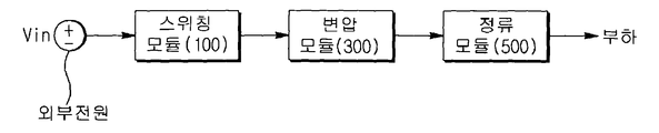
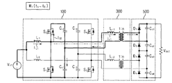
- FIG. 1 is a block diagram illustrating an overall configuration of a boost type DC-DC converter according to an embodiment of the present invention.
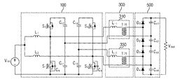
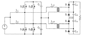
- FIG. 2 is a diagram illustrating a circuit of a boosted DC-DC converter according to an embodiment of the present invention.
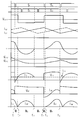
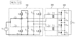
- 3A to 3F are diagrams for describing an operation of a boost type DC-DC converter according to an exemplary embodiment of the present invention.
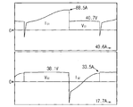
- 4A and 4B are diagrams showing simulation results by a conventional boosted DC-DC converter.
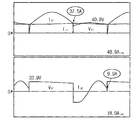
- FIG. 5 is a view showing a simulation result according to the boost type DC-DC converter according to the present invention.
- FIG. 6 is another diagram illustrating a simulation result according to the boost type DC-DC converter according to the present invention.
- FIG. 1 is a block diagram illustrating an overall configuration of a boost type DC-DC converter according to an embodiment of the present invention
- FIG. 2 is a diagram illustrating a circuit of a boost type DC-DC converter according to an embodiment of the present invention.
- a switching module 100 that receives a voltage supplied from a separate external power source and complementarily switches a plurality of switches to output a voltage
- a transformer module 300 which receives the output of the switching module 100 and boosts the output
- a rectifier module 500 that receives the output of the transformer module 300 and performs voltage doubler rectification. It includes.
- the switching module 100 includes: a first inductor L 1 and a second inductor L 2 connected to the separate external power sources and connected in parallel to each other; A first switch S 1 and a second switch S 2 connected in series with the first inductor L 1 and connected in parallel with each other; A third switch S 3 and a fourth switch S 4 connected in series with the second inductor L 2 and connected in parallel with each other; Two first capacitor, which means the first switch capacitor (C r1) and a capacitor (C r3) connected in series with the third switch (S 3) connected in series (S 1) (C r1 , C r3 ); And two capacitors C r2 connected in series to the second switch S 2 and two capacitors C r4 connected in series to the fourth switch S 4 . r2 , C r4 ); It includes.
- the first switch S 1 , the second switch S 2 , the third switch S 3 , and the fourth switch S 4 in the switching module 100 have a predetermined dead-time. It is preferable to have a), and is driven complementarily (Complementary) by a switch drive signal input from the outside.
- any one or more of the first switch S 1 , the second switch S 2 , the third switch S 3 , and the fourth switch S 4 in the switching module 100 are switched. In this case, it is preferable to operate in a duty range of 0 to 1 through a predetermined dead time.
- the first switch S 1 , the second switch S 2 , the third switch S 3 , and the fourth switch S 4 are preferably MOSFETs (Metal Oxide Semiconductor Field-Effect Transistors).
- element values of the first capacitor that is, the capacitor C r1 connected in series with the first switch S 1 and the capacitor C r3 connected in series with the third switch S 3 , may be The same thing is preferable, and the device value of the first capacitor is preferably determined by the following equation.
- Equation 1 C 1 is the element value of the first capacitor, L r1 is the resonance inductance value of the first transformer 310, T s is the period value of the switching drive signal, D nom is The duty value that is set for the converter to operate optimally.
- an element of the capacitor C r2 connected in series to the second capacitor that is, the second switch S 2 and the capacitor C r4 connected in series to the fourth switch S 4 .
- the value is preferably the same, and the device value of the second capacitor is preferably determined by the following equation.
- Equation 2 C 2 is the element value of the second capacitor, L r1 is the resonance inductance value of the first transformer 310, T s is the period value of the switching drive signal, D nom is The duty value that is set for the converter to operate optimally.
- the boost-type DC-DC converter according to the present invention reduces the turn-off current of the switch by using the internal inductance of the transformer module and the resonance generated by the first and second capacitors.
- the imbalance of the phase current and the magnetization current offset can be eliminated.
- a fourth capacitor C q connected in parallel to at least one of the first switch S 1 , the second switch S 2 , the third switch S 3 , and the fourth switch S 4 . ; It is preferable to further include. As shown in FIG. 2, one fourth capacitor C q is connected to the first switch S 1 and the third switch S 3 , respectively, but is not limited thereto.
- the fourth capacitor C q is connected in parallel to one of the first switch S 1 and the second switch S 2 , and the third switch ( It is preferable to use a total of two fourth capacitors C q by allowing the fourth capacitor C q to be connected to one of S 3 ) and the fourth switch S 4 in parallel, but is not limited thereto. No.
- the fourth capacitor C q has the first switch S when the first switch S 1 and the third switch S 3 are turned on or turned off. 1 ) and by reducing the time-dependent change (dv / dt) of the voltage applied to the third switch (S 3 ), thereby reducing the switching loss.
- the primary side line of the first transformer 310 is the A capacitor C r1 connected in series with a first inductor L 1
- a neutral line of the first transformer 310 is connected in series with the first switch S 1 of the two first capacitors, and the two second capacitors.
- the two capacitors are connected between the capacitor (C r2 ) connected in series to the second switch (S 2 ).
- the primary side line of the second transformer 330 is connected in series with the second inductor L 2 , and the neutral line of the second transformer 330 is the third switch S 3 of the first capacitor.
- a capacitor C r3 connected in series to a capacitor C r4 connected in series to the fourth switch S 4 of the second capacitor, and connected to the first transformer 310 and the second transformer 330.
- the secondary side of the) is preferably connected to the rectification module 500.
- the voltage transfer ratio of the transformer module 300 is preferably determined by the following equation in consideration of the leakage inductance of the transformer module 300.
- n is the turn ratio of the transformer module 300
- L k is the resonance inductance L r1 of the first transformer 310 or the resonance inductance L r2 of the second transformer 330. It has the same value as, D is the duty ratio, R o is the output resistance, f s is the switching frequency.
- the rectifier module 500 the first diode (D 1 ) which is connected in series with the secondary side of the first transformer (310);
- the first transformer 310 is connected in series with the secondary side of the first diode a second diode (D 2) is parallel connected with the (D 1);
- a third diode D 3 connected in series with the secondary side of the second transformer 330;
- a fourth diode D 4 connected in series with the secondary side of the second transformer 330 and connected in parallel with the third diode D 3 ;
- a capacitor (C o1 ) connected in series with the first diode (D 1 ), a capacitor (C o2 ) connected in series with the second diode (D 2 ), and a capacitor connected in series with the third diode (D 3 ).
- 3A to 3F are diagrams for describing an operation of a boost type DC-DC converter according to an exemplary embodiment of the present invention.
- M 1 section (t 1 to t 2 ), M 2 section (t 2 to t 3 ), M 3 section (t 3 to t 4 ), M 4 section (t 4 to t 5 ), and It is divided into M 5 sections (t 5 ⁇ t 6 ), the operation of the step-up DC-DC converter according to the present invention for each section described with reference to Figures 3b to 3f as follows.
- S 2 starts at a time point t 1 at which the first diode D 1 is rapidly decreased and the current I r1 flowing in the resonance inductance L r1 of the first transformer 310 decreases rapidly.
- the current I D1 flowing through) decreases with the same slope. Accordingly, as the internal diode becomes conductive, the first switch S 1 is turned on by the zero voltage switching ZVS, and the current I flowing through the resonance inductance L r1 of the first transformer 310. When r1 ) becomes 0, the first diode D 1 is turned off by zero current switching (hereinafter, referred to as 'ZCS') and the section ends.
- 'ZCS' zero current switching
- the operation of the step-up DC-DC converter according to the present invention in the M 2 section (t 2 ⁇ t 3 ) with reference to Figure 3c, after the operation of the M 1 section is finished, the first Resonance occurs by the resonance inductance L r1 of the transformer 310 and the first capacitor C r1 connected in series with the first switch S 1 , and flows through the resonance inductance of the first transformer 310.
- the sum of the current I r1 and the current I L1 flowing in the first inductor L 1 flows to the first switch S 1 .
- the second diode D 2 is zero.
- the section is turned off by the current switching (ZCS).
- FIGS. 4A and 4B are diagrams showing a simulation result by a conventional boosted DC-DC converter
- FIG. 5 is a diagram showing a simulation result by a boosted DC-DC converter according to the present invention
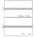
- the turn-off current value of the first switch S 1 according to the structure of the boost type DC-DC converter according to the present invention is 37.5 [A]
- the conventional boosted voltage shown in FIG. 4A is shown. It can be seen that the turn-off current value of the first switch S 1 according to the structure of the type DC-DC converter is reduced compared to 88.5 [A].
Landscapes
- Engineering & Computer Science (AREA)
- Power Engineering (AREA)
- Dc-Dc Converters (AREA)
Description
본 발명은 승압형 DC-DC 컨버터에 관한 것으로, 보다 상세하게는 내부에 포함된 공진 커패시터(Capacitor)에 의해 발생하는 공진현상을 이용하여 스위칭 손실을 감소시켜 효율을 향상하며, 턴오프전류를 감소시켜 신뢰성이 향상된 승압형 DC-DC 컨버터에 관한 것이다.
일반적으로 DC-DC 컨버터의 경우 크게 전압원 컨버터와 전류원 컨버터로 분류되며, 승압형 컨버터의 경우 기본적으로 전압원 컨버터에 비해 승압비가 높으며 전류리플이 작은 전류원 컨버터가 주로 사용되고 있다. 상기 전류원 컨버터의 대표적인 토폴로지(Topology)의 경우 풀브리지(Full-bridge) 컨버터, 푸시풀(Push-pull) 컨버터 및 하프브리지(Half-bridge) 컨버터가 있다.
상기 풀브리지(Full-bridge) 컨버터의 경우 다른 토폴로지에 비해 스위치 수가 많다는 단점이 있으며, 상기 푸시풀(Push-pull) 컨버터의 경우 변압 모듈에 탭이 필요하여 제작이 어려운 단점이 있다. 따라서, 인터리빙(Interleaving) 효과에 의해 전류리플이 감소하며 인덕터의 분산배치에 따라 열이 분산되며 승압비가 높다는 장점이 있는 하프브리지(Half-bridge) 컨버터가 많이 채택되고 있다.
이러한 승압형 DC-DC 컨버터에 관해 종래기술(한국출원 2008-0084758호) 등이 출원된 바 있으나, 본 발명은 상기 종래기술과 달리 공진현상을 이용하여 스위칭 손실을 감소시켜 효율이 향상된 DC-DC 컨버터에 관해 이하와 같이 개시한다.
본 발명의 목적은, 내부에 포함된 공진커패시터(Capacitor) 및 변압기의 누설인덕턴스에 의해 발생하는 공진현상을 이용하여 턴오프 전류를 저감함과 더불어 각 상 전류의 불균형 및 자화전류 오프셋을 상기 변압기에 직렬연결된 커패시터를 통해 제거하여 효율이 향상된 DC-DC 컨버터를 제공함에 있다.
본 발명에 따른 승압형 DC-DC 컨버터는, 별도의 외부전원에서 공급되는 전압을 입력받아 복수개의 스위치를 상보적으로 스위칭하여 전압을 출력하는 스위칭 모듈; 상기 스위칭 모듈의 출력을 입력받아 승압하여 출력하는 변압 모듈; 및 상기 변압 모듈의 출력을 입력받아 전압 더블러(Voltage doubler) 정류를 수행하는 정류 모듈; 을 포함하되, 상기 스위칭 모듈은, 상기 별도의 외부전원과 연결되어 있으며, 서로 병렬로 연결된 제1 인덕터 및 제2 인덕터; 상기 제1 인덕터와 직렬연결되어 있으며, 서로 병렬로 연결된 제1 스위치 및 제2 스위치; 상기 제2 인덕터와 직렬연결되어 있으며, 서로 병렬로 연결된 제3 스위치 및 제 4 스위치; 상기 제1 스위치 및 상기 제3 스위치 각각에 직렬로 연결되어 있는 2개의 제1 커패시터; 및상기 제2 스위치 및 상기 제4 스위치 각각에 직렬로 연결되어 있는 2개의 제2 커패시터; 를 포함한다.
이때, 상기 변압 모듈은, 상기 스위칭 모듈과 연결된 제1 변압기 및 제2 변압기를 포함하되, 상기 제1 변압기의 1차측 선이 상기 제1 인덕터와 직렬연결되고, 상기 제1 변압기의 중성선은 상기 제1 스위치에 직렬연결된 상기 제1 커패시터 및 상기 제2 스위치에 직렬연결된 상기 제2 커패시터 간에 연결되며, 상기 제2 변압기의 1차측 선이 상기 제2 인덕터와 직렬연결되고, 상기 제2 변압기의 중성선은 상기 제3 스위치에 직렬연결된 제1 커패시터 및 상기 제4 스위치에 직렬연결된 제2 커패시터 간에 연결되며, 상기 제1 변압기 및 상기 제2 변압기의 2차측은 상기 정류 모듈과 연결되는 것을 특징으로 하는 것이 바람직하다.
이때, 상기 정류 모듈은, 상기 제1 변압기의 2차측과 직렬연결되어 있는 제1 다이오드; 상기 제1 변압기의 2차측과 직렬연결되며 상기 제1 다이오드와 병렬연결되는 제2 다이오드; 상기 제2 변압기의 2차측과 직렬연결되어 있는 제3 다이오드; 상기 제2 변압기의 2차측과 직렬연결되며 상기 제3 다이오드와 병렬연결되는 제4 다이오드; 및 상기 제1 다이오드, 상기 제2 다이오드, 상기 제3 다이오드 및 상기 제4 다이오드 각각에 직렬연결되는 제3 커패시터; 를 포함하는 것이 바람직하다.
이때, 상기 스위칭 모듈은, 상기 제1 스위치, 제2 스위치, 제3 스위치 및 제4 스위치 중 적어도 어느 하나 이상에 병렬로 연결된 제4 커패시터; 를 더 포함하는 것이 바람직하다.
이때, 상기 제1 스위치, 제2 스위치, 제3 스위치 및 제4 스위치는 소정의 데드 타임(Dead-time)을 가지며, 외부에서 입력되는 스위치 구동신호에 의해 상보적(Complementary)으로 구동되는 것이 바람직하다.
이때, 상기 스위칭 모듈은, 상기 제1 스위치, 상기 제2 스위치, 상기 제3 스위치 및 상기 제4 스위치 중 어느 하나 이상이 스위칭되는 경우, 소정의 데드 타임(Dead-time)을 통해 0~1의 듀티 범위에서 동작하는 것이 바람직하다.
이때, 상기 제1 스위치, 제2 스위치, 제3 스위치 및 제4 스위치는 MOSFET(Metal Oxide Semiconductor Field-Effect Transistor) 인 것이 바람직하다.
본 발명에 따르면, 내부에 포함된 커패시터(Capacitor)에 의해 발생하는 부분적 공진현상을 이용하여 스위칭 손실을 저감할 수 있고, 턴온(Turn-on) 시 영전압스위칭(Zero Voltage Switching, 이하, 'ZVS')이 가능하고 턴오프(Turn-off) 시 전류를 저감하여 스위칭 소자의 수명저감을 방지할 수 있으며, 나아가 각 상 전류의 불균형을 해소할 수 있는 효과도 있다.
도 1은 본 발명의 실시예에 따른 승압형 DC-DC 컨버터의 전체구성을 설명하기 위한 블록도이다.
도 2는 본 발명의 실시예에 따른 승압형 DC-DC 컨버터의 회로를 예시한 도면이다.
도 3a 내지 도 3f는 본 발명의 실시예에 따른 승압형 DC-DC 컨버터의 동작을 설명하기 위한 도면이다.
도 4a 및 도 4b는 기존의 승압형 DC-DC 컨버터에 의한 시뮬레이션 결과를 나타낸 도면이다.
도 5는 본 발명에 따른 승압형 DC-DC 컨버터에 따른 시뮬레이션 결과를 나타낸 도면이다.
도 6은 본 발명에 따른 승압형 DC-DC 컨버터에 따른 시뮬레이션 결과를 나타낸 다른 도면이다.
본 발명의 실시를 위한 구체적인 내용을 설명하기에 앞서, 본 발명의 기술적 요지와 직접적 관련이 없는 구성에 대해서는 본 발명의 기술적 요지를 흩뜨리지 않는 범위 내에서 생략하였음에 유의하여야 할 것이다. 또한, 본 명세서 및 청구범위에 사용된 용어 또는 단어는 발명자가 자신의 발명을 최선의 방법으로 설명하기 위해 적절한 용어의 개념을 정의할 수 있다는 원칙에 입각하여 본 발명의 기술적 사상에 부합하는 의미와 개념으로 해석되어야 할 것이다.
이하, 본 발명에 따른 승압형 DC-DC 컨버터의 구성을 첨부한 예시도면을 참조하여 상세히 설명한다. 도 1은 본 발명의 실시예에 따른 승압형 DC-DC 컨버터의 전체구성을 설명하기 위한 블록도이며, 도 2는 본 발명의 실시예에 따른 승압형 DC-DC 컨버터의 회로를 예시한 도면이다.
본 발명에 따른 승압형 DC-DC 컨버터의 경우, 도 1에 도시된 바와 같이 별도의 외부전원에서 공급되는 전압을 입력받아 복수개의 스위치를 상보적으로 스위칭하여 전압을 출력하는 스위칭 모듈(100); 상기 스위칭 모듈(100)의 출력을 입력받아 승압하여 출력하는 변압 모듈(300); 및 상기 변압 모듈(300)의 출력을 입력받아 전압 더블러(Voltage doubler) 정류를 수행하는 정류 모듈(500); 을 포함한다.
도 2를 참조하여 보다 구체적으로 설명하면, 상기 스위칭 모듈(100)은, 상기 별도의 외부전원과 연결되어 있으며, 서로 병렬로 연결된 제1 인덕터(L1) 및 제2 인덕터(L2); 상기 제1 인덕터(L1)와 직렬연결되어 있으며, 서로 병렬로 연결된 제1 스위치(S1) 및 제2 스위치(S2); 상기 제2 인덕터(L2)와 직렬연결되어 있으며, 서로 병렬로 연결된 제3 스위치(S3) 및 제 4 스위치(S4); 상기 제1 스위치(S1)에 직렬로 연결되어 있는 커패시터(Cr1) 및 상기 제3 스위치(S3)에 직렬로 연결되어 있는 커패시터(Cr3)를 의미하는 2개의 제1 커패시터(Cr1,Cr3) ; 및 상기 제2 스위치(S2)에 직렬로 연결되어 있는 커패시터(Cr2) 및 상기 제4 스위치(S4)에 직렬로 연결되어 있는 커패시터(Cr4)를 의미하는 2개의 제2 커패시터(Cr2,Cr4); 를 포함한다.
이때, 상기 스위칭 모듈(100) 내 상기 제1 스위치(S1), 제2 스위치(S2), 제3 스위치(S3) 및 제4 스위치(S4)는 소정의 데드 타임(Dead-time)을 가지며, 외부에서 입력되는 스위치 구동신호에 의해 상보적(Complementary)으로 구동되는 것이 바람직하다.
그리고, 상기 스위칭 모듈(100) 내 상기 제1 스위치(S1), 상기 제2 스위치(S2), 상기 제3 스위치(S3) 및 상기 제4 스위치(S4) 중 어느 하나 이상이 스위칭되는 경우, 소정의 데드 타임(Dead-time)을 통해 0~1의 듀티 범위에서 동작하는 것이 바람직하다.
이때, 상기 제1 스위치(S1), 제2 스위치(S2), 제3 스위치(S3) 및 제4 스위치(S4)는 MOSFET(Metal Oxide Semiconductor Field-Effect Transistor) 인 것이 바람직하다.
이때, 상기 제1 커패시터, 즉, 상기 제1 스위치(S1)에 직렬연결되어 있는 커패시터(Cr1) 및 상기 제3 스위치(S3)에 직렬연결되어 있는 커패시터(Cr3)의 소자값은 동일한 것이 바람직하며, 상기 제1 커패시터의 소자값은 다음과 같은 수식에 의해 결정되는 것이 바람직하다.
수학식 1 
상기 수학식 1에 있어서, C1은 상기 제1 커패시터의 소자값이며, Lr1은 상기 제1 변압기(310)의 공진인덕턴스 값이며, Ts는 스위칭 구동신호의 주기값이며, Dnom는 상기 컨버터가 최적으로 동작하기 위해 설정되는 듀티값을 의미한다.
이때, 상기 제2 커패시터, 즉, 상기 제2 스위치(S2)에 직렬로 연결되어 있는 커패시터(Cr2) 및 상기 제4 스위치(S4)에 직렬로 연결되어 있는 커패시터(Cr4)의 소자값은 동일한 것이 바람직하며, 상기 제2 커패시터의 소자값은 다음과 같은 수식에 의해 결정되는 것이 바람직하다.
수학식 2 
상기 수학식 2에 있어서, C2은 상기 제2 커패시터의 소자값이며, Lr1은 상기 제1 변압기(310)의 공진인덕턴스값이며, Ts는 스위칭 구동신호의 주기값이며, Dnom는 상기 컨버터가 최적으로 동작하기 위해 설정되는 듀티값을 의미한다.
이에 따라, 본 발명에 따른 승압형 DC-DC 컨버터는, 변압 모듈의 내부 인턱턴스와 상기 제1 커패시터 및 제2 커패시터에 의해 발생하는 공진현상을 이용하여 스위치의 턴오프 전류를 저감하며, 아울러 각 상 전류의 불균형 및 자화전류 오프셋을 제거할 수 있다.
이때, 상기 제1 스위치(S1), 제2 스위치(S2), 제3 스위치(S3) 및 제4 스위치 (S4) 중 적어도 어느 하나 이상에 병렬로 연결된 제4 커패시터(Cq); 를 더 포함하는 것이 바람직하다. 도 2에 도시된 경우와 같이 상기 제1 스위치(S1) 및 상기 제3 스위치(S3)에 각각 1개의 제4 커패시터(Cq)가 병렬연결되어 있으나 이에 한정되지 아니한다.
예를 들어, 도 2에 도시된 바와 같이 상기 제1 스위치(S1) 및 상기 제2 스위치(S2) 중 어느 하나에 상기 제4 커패시터(Cq)가 병렬연결되며, 상기 제3 스위치(S3) 및 제4 스위치(S4) 중 어느 하나에 상기 제4 커패시터(Cq)가 병렬연결되도록 하여, 총 2개의 제4 커패시터(Cq)를 사용하는 것이 바람직하나, 다만 이에 한정되지 아니한다.
상기 제4 커패시터(Cq)는 상기 제1 스위치(S1) 및 상기 제3 스위치(S3)가 턴온(Turn-on) 또는 턴오프(Turn-off)되는 시점에 상기 제1 스위치(S1) 및 상기 제3 스위치(S3)에 인가되는 전압의 시간당 변화(dv/dt)를 완만하게 함으로써, 스위칭 손실을 감소하는 기능을 수행한다.
다음으로, 상기 변압 모듈(300)의 경우, 상기 스위칭 모듈(100)과 연결된 제1 변압기(310) 및 제2 변압기(330)를 포함하되, 상기 제1 변압기(310)의 1차측 선은 상기 제1 인덕터(L1)와 직렬연결되고, 상기 제1 변압기(310)의 중성선은 상기 2개의 제1 커패시터 중 상기 제1 스위치(S1)에 직렬연결된 커패시터(Cr1) 및 상기 2개의 제2 커패시터 중 상기 제2 스위치(S2)에 직렬연결된 커패시터(Cr2) 간에 연결된다.
그리고, 상기 제2 변압기(330)의 1차측 선은 상기 제2 인덕터(L2)와 직렬연결되고, 상기 제2 변압기(330)의 중성선은 상기 제1 커패시터 중 상기 제3 스위치(S3)에 직렬연결되어 있는 커패시터(Cr3) 및 상기 제2 커패시터 중 상기 제4 스위치(S4)에 직렬연결된 커패시터(Cr4) 간에 연결되며, 상기 제1 변압기(310) 및 상기 제2 변압기(330)의 2차측은 상기 정류 모듈(500)과 연결되는 것이 바람직하다.
이때, 상기 변압 모듈(300)의 전압전달비는, 상기 변압 모듈(300)의 누설인덕턴스를 고려하여 하기의 수학식에 의해 결정되는 것이 바람직하다.
수학식 3 
상기 수학식 3에 있어서, n은 변압 모듈(300)의 턴수비, Lk는 즉, 제1 변압기(310)의 공진인덕턴스(Lr1) 또는 제2 변압기(330)의 공진인덕턴스(Lr2)와 동일한 값을 가지며, D는 듀티 비, Ro는 출력저항, fs는 스위칭 주파수를 의미한다.
마지막으로, 상기 정류 모듈(500)은, 상기 제1 변압기(310)의 2차측과 직렬연결되어 있는 제1 다이오드(D1); 상기 제1 변압기(310)의 2차측과 직렬연결되며 상기 제1 다이오드(D1)와 병렬연결되는 제2 다이오드(D2); 상기 제2 변압기(330)의 2차측과 직렬연결되어 있는 제3 다이오드(D3); 상기 제2 변압기(330)의 2차측과 직렬연결되며 상기 제3 다이오드(D3)와 병렬연결되는 제4 다이오드(D4); 및 상기 제1 다이오드(D1)에 직렬연결되는 커패시터(Co1), 상기 제2 다이오드(D2)에 직렬연결되는 커패시터(Co2), 상기 제3 다이오드(D3)에 직렬연결되는 커패시터(Co3) 및 상기 제4 다이오드(D4)에 직렬연결되는 커패시터(Co4)를 포함하는 제3 커패시터(Co1,Co2,Co3,Co4); 로 구성된다.
이하, 본 발명에 따른 승압형 DC-DC 컨버터의 동작을 첨부한 예시도면을 참조하여 상세히 설명한다. 도 3a 내지 도 3f는 본 발명의 실시예에 따른 승압형 DC-DC 컨버터의 동작을 설명하기 위한 도면이다.
설명하기에 앞서, 본 발명에 따른 승압형 DC-DC 컨버터의 경우, 도 3a에 도시된 바와 같은 동작파형을 갖는 것이 바람직하며, 상기 도 3b 내지 도 3f에는 전술한 제4 커패시터(Cq)의 도시가 생략되어 있다.
상기 동작파형의 경우 크게 M1 구간(t1~t2), M2 구간(t2~t3), M3 구간(t3~t4), M4 구간(t4~t5) 및 M5 구간(t5~t6)으로 나뉘게 되며, 상기 구간별로 본 발명에 따른 승압형 DC-DC 컨버터의 동작을 도 3b 내지 도 3f를 참조하여 설명하면 다음과 같다.
먼저, 본 발명에 따른 승압형 DC-DC 컨버터의 상기 M1 구간(t1~t2) 내 동작에 대해 도 3b를 참조하여 설명하면, 외부에서 입력되는 스위칭 구동신호에 의해 상기 제2 스위치(S2)가 오프(Off)되는 시점(t1)에서 시작되며, 제1 변압기(310)의 공진인덕턴스(Lr1)에 흐르는 전류(Ir1)가 급격히 감소함과 동시에 제1 다이오드(D1)에 흐르는 전류(ID1)가 동일한 기울기로 감소한다. 이에 따라서, 내부 다이오드가 도통되게 됨에 따라 상기 제1 스위치(S1)가 영전압스위칭(ZVS)에 의해 턴온되게 되며, 상기 제1 변압기(310)의 공진인덕턴스(Lr1)에 흐르는 전류(Ir1)가 0이 될때 상기 제1 다이오드(D1)가 영전류스위칭(Zero Current Switching; 이하, 'ZCS')에 의해 턴오프되며 구간이 종료된다.
다음으로, 본 발명에 따른 승압형 DC-DC 컨버터의 상기 M2 구간(t2~t3) 내 동작에 대해 도 3c를 참조하여 설명하면, 상기 M1 구간의 동작이 종료된 이후 상기 제1 변압기(310)의 공진인덕턴스(Lr1)와 상기 제1 스위치(S1)에 직렬연결된 제1 커패시터(Cr1)에 의해 공진이 발생하게 되고, 상기 제1 변압기(310)의 공진인덕턴스에 흐르는 전류(Ir1)와 상기 제1 인덕터(L1)에 흐르는 전류(IL1)의 합이 상기 제1 스위치(S1)로 흐르게 된다. 이후, 상기 제1 스위치(S1)에 흐르는 전류(IS1)와 상기 제1 인덕터(L1)에 흐르는 전류(IL1)가 같은 값을 가질 때, 상기 제2 다이오드(D2)가 영전류스위칭(ZCS)에 의해 턴오프되며 구간이 종료된다.
다음으로, 본 발명에 따른 승압형 DC-DC 컨버터의 상기 M3 구간(t3~t4) 내 동작에 대해 도 3d를 참조하여 설명하면, 상기 M2 구간의 동작이 종료된 시점(t3)이후 상기 제1 인덕터(L1)에 흐르는 전류(IL1)가 모두 상기 제1 스위치(S1)에 흐르게 되며, 외부에서 입력되는 스위칭 구동신호에 의해 상기 제1 스위치(S1)가 오프(Off)되는 시점(t4)에서 구간이 종료된다.
다음으로, 본 발명에 따른 승압형 DC-DC 컨버터의 상기 M4 구간(t4~t5) 내 동작에 대해 도 3e를 참조하여 설명하면, 상기 M3 구간의 동작이 종료되어 상기 제1 스위치(S1)가 오프(Off)된 이후, 내부 다이오드가 도통되게 됨에 따라 상기 제2 스위치(S2)가 영전압스위칭(ZVS)에 의해 턴온되며 구간이 종료된다.
마지막으로, 본 발명에 따른 승압형 DC-DC 컨버터의 상기 M5 구간(t5~t6) 내 동작에 대해 도 3f를 참조하여 설명하면, 상기 M4 구간의 동작이 종료된 이후 상기 제1 변압기(310)의 공진인덕턴스(Lr1)와 상기 제2 스위치(S2)에 직렬연결된 제2 커패시터(Cr2)에 의해 공진이 발생하게 된다. 그리고, 상기 제1 인덕터(L1)에 흐르는 전류(IL1)와 상기 제1 변압기(310)의 공진인덕턴스(Lr1)에 흐르는 전류(Ir1)의 차가 상기 제2 스위치(S2)로 흐르는 전류(IS2)가 되며, 외부에서 입력되는 스위칭 구동신호에 의해 전술한 제2 스위치가 오프(Off)되는 시점(t6)에 구간이 종료된다.
이하, 기존의 승압형 DC-DC 컨버터와 본 발명에 따른 승압형 DC-DC 컨버터의 턴오프 전류를 시뮬레이션한 결과를 첨부한 예시도면을 토대로 설명한다. 도 4a 및 도 4b는 기존의 승압형 DC-DC 컨버터에 의한 시뮬레이션 결과를 나타낸 도면이고, 도 5는 본 발명에 따른 승압형 DC-DC 컨버터에 따른 시뮬레이션 결과를 나타낸 도면이며, 도 6은 본 발명에 따른 승압형 DC-DC 컨버터에 따른 시뮬레이션 결과를 나타낸 다른 도면이다.
설명하기에 앞서, 도 4a에 도시한 기존의 승압형 DC-DC 컨버터 및 본 발명에 따른 승압형 DC-DC 컨버터의 경우 동일조건(입력전압(Vin)= 16V, 출력전압(Vout) = 360V, 스위칭 주파수(fs) = 30㎑, 입력전류의 리플율(△Iin) = 3%, 출력전압의 리플율(△Vout) = 2%)에서 시뮬레이션을 수행하였다
그 결과, 도 5에 도시한 바와 같이 본 발명에 따른 승압형 DC-DC 컨버터의 구조에 따른 제1 스위치(S1)의 턴오프 전류값은 37.5[A]로 도 4a에 도시한 기존의 승압형 DC-DC 컨버터의 구조에 따른 제1 스위치(S1)의 턴오프 전류값이 88.5[A]임에 비해 저감됨을 알 수 있다.
또한, 도 6에 도시한 바와 같이 본 발명에 따른 승압형 DC-DC 컨버터의 경우, 제1 인덕터(L1) 및 제2 인덕터(L2)에 흐르는 전류가 상기 변압 모듈(300)에 직렬연결된 제3 커패시터(Co1, Co2, Co3, Co4)에 의해 불균형이 없이 잘 제어되고 있는 것을 알 수 있다.
이상으로, 본 발명의 기술적 사상을 예시하기 위한 바람직한 실시예와 관련하여 설명하고 도시하였으나, 본 발명은 상기 설명 및 도시 대로의 구성 및 작용에만 국한되는 것이 아니다. 아울러 본 발명의 기술적 사상의 범주를 일탈하지 않는 범위 내에서 다수의 변경 및 수정이 가능함을 당업자는 잘 이해할 수 있을 것이다. 따라서 모든 적절한 변경 및 수정이 가해진 발명 및 본 발명의 균등물에 속하는 발명들도 본 발명에 속하는 것으로 간주되어야 할 것이다.
Claims (7)
- 별도의 외부전원에서 공급되는 전압을 승압시키는 승압형 DC-DC 컨버터에 있어서,상기 별도의 외부전원에서 공급되는 전압을 입력받아 복수개의 스위치를 상보적으로 스위칭하여 전압을 출력하는 스위칭 모듈(100); 상기 스위칭 모듈(100)의 출력을 입력받아 승압하여 출력하는 변압 모듈(300); 및 상기 변압 모듈(300)의 출력을 입력받아 전압 더블러(Voltage doubler) 정류를 수행하는 정류 모듈(500); 을 포함하되,상기 스위칭 모듈(100)은,상기 별도의 외부전원과 연결되어 있으며, 서로 병렬로 연결된 제1 인덕터(L1) 및 제2 인덕터(L2);상기 제1 인덕터(L1)와 직렬연결되어 있으며, 서로 병렬로 연결된 제1 스위치(S1) 및 제2 스위치(S2);상기 제2 인덕터(L2)와 직렬연결되어 있으며, 서로 병렬로 연결된 제3 스위치(S3) 및 제 4 스위치(S4);상기 제1 스위치(S1) 및 상기 제3 스위치(S3) 각각에 직렬로 연결되어 있는 2개의 제1 커패시터(Cr1, Cr3); 및상기 제2 스위치(S2) 및 상기 제4 스위치(S4) 각각에 직렬로 연결되어 있는 2개의 제2 커패시터(Cr2, Cr4); 를 포함하는 것을 특징으로 하는 승압형 DC-DC 컨버터.
- 제 1 항에 있어서,상기 변압 모듈(300)은,상기 스위칭 모듈(100)과 연결된 제1 변압기(310) 및 제2 변압기(330)를 포함하되,상기 제1 변압기(310)의 1차측 선이 상기 제1 인덕터(L1)와 직렬연결되고, 상기 제1 변압기(310)의 중성선은 상기 제1 스위치(S1)에 직렬연결된 상기 제1 커패시터(Cr1) 및 상기 제2 스위치(S2)에 직렬연결된 상기 제2 커패시터(Cr2) 간에 연결되며,상기 제2 변압기(330)의 1차측 선이 상기 제2 인덕터(L2)와 직렬연결되고, 상기 제2 변압기(330)의 중성선은 상기 제3 스위치(S3)에 직렬연결된 제1 커패시터(Cr3) 및 상기 제4 스위치(S4)에 직렬연결된 제2 커패시터(Cr4) 간에 연결되며,상기 제1 변압기(310) 및 상기 제2 변압기(330)의 2차측은 상기 정류 모듈(500)과 연결되는 것을 특징으로 하는 승압형 DC-DC 컨버터.
- 제 2 항에 있어서,상기 정류 모듈(500)은,상기 제1 변압기(310)의 2차측과 직렬연결되어 있는 제1 다이오드(D1);상기 제1 변압기(310)의 2차측과 직렬연결되며 상기 제1 다이오드(D1)와 병렬연결되는 제2 다이오드(D2);상기 제2 변압기(330)의 2차측과 직렬연결되어 있는 제3 다이오드(D3);상기 제2 변압기(330)의 2차측과 직렬연결되며 상기 제3 다이오드(D3)와 병렬연결되는 제4 다이오드(D4); 및상기 제1 다이오드(D1),상기 제2 다이오드(D2),상기 제3 다이오드(D3) 및 상기 제4 다이오드(D4) 각각에 직렬연결되는 제3 커패시터(Co1, Co2, Co3, Co4); 를 포함하는 것을 특징으로 하는 승압형 DC-DC 컨버터.
- 제 1 항에 있어서,상기 스위칭 모듈(100)은,상기 제1 스위치(S1), 상기 제2 스위치(S2), 상기 제3 스위치(S3) 및 상기 제4 스위치(S4) 중 적어도 어느 하나 이상에 병렬로 연결된 제4 커패시터(Cq); 를 더 포함하는 것을 특징으로 하는 승압형 DC-DC 컨버터.
- 제 1 항에 있어서,상기 제1 스위치(S1), 상기 제2 스위치(S2), 상기 제3 스위치(S3) 및 상기 제4 스위치(S4)는 소정의 데드 타임(Dead-time)을 가지며, 외부에서 입력되는 스위치 구동신호에 의해 상보적(Complementary)으로 구동되는 것을 특징으로 하는 승압형 DC-DC 컨버터.
- 제 1 항에 있어서,상기 스위칭 모듈(100)은,상기 제1 스위치(S1), 상기 제2 스위치(S2), 상기 제3 스위치(S3) 및 상기 제4 스위치(S4) 중 어느 하나 이상이 스위칭되는 경우, 소정의 데드 타임(Dead-time)을 통해 0~1의 듀티 범위에서 동작하는 것을 특징으로 하는 승압형 DC-DC 컨버터.
- 제 1 항 내지 제 6 항 중 어느 한 항에 있어서,상기 제1 스위치(S1), 상기 제2 스위치(S2), 상기 제3 스위치(S3) 및 상기 제4 스위치(S4)는 MOSFET(Metal Oxide Semiconductor Field-Effect Transistor) 인 것을 특징으로 하는 승압형 DC-DC 컨버터.
Applications Claiming Priority (2)
| Application Number | Priority Date | Filing Date | Title |
|---|---|---|---|
| KR1020110146735A KR101240098B1 (ko) | 2011-12-30 | 2011-12-30 | 승압형 dc-dc 컨버터 |
| KR10-2011-0146735 | 2011-12-30 |
Publications (1)
| Publication Number | Publication Date |
|---|---|
| WO2013100674A1 true WO2013100674A1 (ko) | 2013-07-04 |
Family
ID=48181223
Family Applications (1)
| Application Number | Title | Priority Date | Filing Date |
|---|---|---|---|
| PCT/KR2012/011657 Ceased WO2013100674A1 (ko) | 2011-12-30 | 2012-12-28 | 승압형 dc-dc 컨버터 |
Country Status (2)
| Country | Link |
|---|---|
| KR (1) | KR101240098B1 (ko) |
| WO (1) | WO2013100674A1 (ko) |
Cited By (1)
| Publication number | Priority date | Publication date | Assignee | Title |
|---|---|---|---|---|
| EP3476033A4 (en) * | 2016-07-27 | 2020-02-26 | Murata Manufacturing Co., Ltd. | Multi-phase llc converters connected in parallel and series |
Citations (5)
| Publication number | Priority date | Publication date | Assignee | Title |
|---|---|---|---|---|
| US4618919A (en) * | 1984-10-04 | 1986-10-21 | Sperry Corporation | Topology for miniature power supply with low voltage and low ripple requirements |
| US5231563A (en) * | 1990-09-07 | 1993-07-27 | Itt Corporation | Square wave converter having an improved zero voltage switching operation |
| KR20090033087A (ko) * | 2007-09-27 | 2009-04-01 | 서울산업대학교 산학협력단 | 승압형 고효율 dc-dc 컨버터 |
| KR20100078122A (ko) * | 2008-12-30 | 2010-07-08 | 서울산업대학교 산학협력단 | 고승압비를 갖는 비절연 소프트 스위칭 dcdc 컨버터 |
| KR20110077955A (ko) * | 2009-12-30 | 2011-07-07 | 두산중공업 주식회사 | 승압비 및 전력용량 증대비에 따른 확장형 비절연 소프트 스위칭 다상 dc-dc 컨버터 |
-
2011
- 2011-12-30 KR KR1020110146735A patent/KR101240098B1/ko active Active
-
2012
- 2012-12-28 WO PCT/KR2012/011657 patent/WO2013100674A1/ko not_active Ceased
Patent Citations (5)
| Publication number | Priority date | Publication date | Assignee | Title |
|---|---|---|---|---|
| US4618919A (en) * | 1984-10-04 | 1986-10-21 | Sperry Corporation | Topology for miniature power supply with low voltage and low ripple requirements |
| US5231563A (en) * | 1990-09-07 | 1993-07-27 | Itt Corporation | Square wave converter having an improved zero voltage switching operation |
| KR20090033087A (ko) * | 2007-09-27 | 2009-04-01 | 서울산업대학교 산학협력단 | 승압형 고효율 dc-dc 컨버터 |
| KR20100078122A (ko) * | 2008-12-30 | 2010-07-08 | 서울산업대학교 산학협력단 | 고승압비를 갖는 비절연 소프트 스위칭 dcdc 컨버터 |
| KR20110077955A (ko) * | 2009-12-30 | 2011-07-07 | 두산중공업 주식회사 | 승압비 및 전력용량 증대비에 따른 확장형 비절연 소프트 스위칭 다상 dc-dc 컨버터 |
Cited By (1)
| Publication number | Priority date | Publication date | Assignee | Title |
|---|---|---|---|---|
| EP3476033A4 (en) * | 2016-07-27 | 2020-02-26 | Murata Manufacturing Co., Ltd. | Multi-phase llc converters connected in parallel and series |
Also Published As
| Publication number | Publication date |
|---|---|
| KR101240098B1 (ko) | 2013-03-06 |
Similar Documents
| Publication | Publication Date | Title |
|---|---|---|
| CN203691238U (zh) | 电子变换器以及相关照明系统 | |
| Panov et al. | Design and performance evaluation of low-voltage/high-current DC/DC on-board modules | |
| EP2110937B1 (en) | Insulation type ac-dc converter and led dc power supply device using the same | |
| US9520792B2 (en) | Staggered parallel three-level DC/DC converter and AC/DC converter | |
| US9065349B2 (en) | Control method for bidirectional DC-DC converters | |
| Wu et al. | An active-clamp push–pull converter for battery sourcing applications | |
| KR100983673B1 (ko) | 승압형 dc-dc 컨버터 | |
| US20120044722A1 (en) | Isolated switching converter | |
| Yao et al. | A family of buck-type DC-DC converters with autotransformers | |
| CN114301297B (zh) | 一种功率变换器、增大逆向增益范围的方法、装置、介质 | |
| CN110061636A (zh) | 功率变换装置 | |
| US6853568B2 (en) | Isolated voltage regulator with one core structure | |
| Khalili et al. | Soft-switched asymmetric interleaved WCCI high step-down converter with low-voltage stress | |
| CN106533178A (zh) | 隔离型开关电源和隔离型开关电源控制方法 | |
| US20050180173A1 (en) | Power converter with interleaved topology | |
| WO2018048057A1 (ko) | Dc-dc 컨버터 및 이를 포함하는 2단 전력단 컨버터 | |
| CN107005171A (zh) | 电力变换单元 | |
| CN108712070B (zh) | 基于zcs pwm双向dc-dc cuk变换器、变换系统和方法 | |
| CN208158436U (zh) | 一种同步整流反激式直流-直流电源转换装置 | |
| CN114389458A (zh) | 控制电路以及应用其的开关变换器 | |
| WO2013100674A1 (ko) | 승압형 dc-dc 컨버터 | |
| WO2021107480A1 (ko) | Dc-dc 컨버터 | |
| CN105024554B (zh) | 具有软切换且能降低电流涟波的逆变电路及整流电路 | |
| CN119921575B (zh) | 一种集成三相Boost-LLC拓扑及调制方法 | |
| WO2015174769A1 (ko) | 소프트 스위칭 방식의 영전류 천이형 벅 컨버터 |
Legal Events
| Date | Code | Title | Description |
|---|---|---|---|
| 121 | Ep: the epo has been informed by wipo that ep was designated in this application |
Ref document number: 12862034 Country of ref document: EP Kind code of ref document: A1 |
|
| NENP | Non-entry into the national phase |
Ref country code: DE |
|
| 122 | Ep: pct application non-entry in european phase |
Ref document number: 12862034 Country of ref document: EP Kind code of ref document: A1 |