WO2013099264A1 - Solid-state imaging element, and imaging device - Google Patents
Solid-state imaging element, and imaging device Download PDFInfo
- Publication number
- WO2013099264A1 WO2013099264A1 PCT/JP2012/008392 JP2012008392W WO2013099264A1 WO 2013099264 A1 WO2013099264 A1 WO 2013099264A1 JP 2012008392 W JP2012008392 W JP 2012008392W WO 2013099264 A1 WO2013099264 A1 WO 2013099264A1
- Authority
- WO
- WIPO (PCT)
- Prior art keywords
- pixel
- capacitor
- solid
- imaging device
- signal
- Prior art date
Links
Images


Classifications
-
- H—ELECTRICITY
- H04—ELECTRIC COMMUNICATION TECHNIQUE
- H04N—PICTORIAL COMMUNICATION, e.g. TELEVISION
- H04N25/00—Circuitry of solid-state image sensors [SSIS]; Control thereof
- H04N25/10—Circuitry of solid-state image sensors [SSIS]; Control thereof for transforming different wavelengths into image signals
- H04N25/11—Arrangement of colour filter arrays [CFA]; Filter mosaics
- H04N25/13—Arrangement of colour filter arrays [CFA]; Filter mosaics characterised by the spectral characteristics of the filter elements
- H04N25/134—Arrangement of colour filter arrays [CFA]; Filter mosaics characterised by the spectral characteristics of the filter elements based on three different wavelength filter elements
-
- H—ELECTRICITY
- H04—ELECTRIC COMMUNICATION TECHNIQUE
- H04N—PICTORIAL COMMUNICATION, e.g. TELEVISION
- H04N25/00—Circuitry of solid-state image sensors [SSIS]; Control thereof
- H04N25/40—Extracting pixel data from image sensors by controlling scanning circuits, e.g. by modifying the number of pixels sampled or to be sampled
- H04N25/46—Extracting pixel data from image sensors by controlling scanning circuits, e.g. by modifying the number of pixels sampled or to be sampled by combining or binning pixels
-
- H—ELECTRICITY
- H04—ELECTRIC COMMUNICATION TECHNIQUE
- H04N—PICTORIAL COMMUNICATION, e.g. TELEVISION
- H04N25/00—Circuitry of solid-state image sensors [SSIS]; Control thereof
- H04N25/60—Noise processing, e.g. detecting, correcting, reducing or removing noise
- H04N25/68—Noise processing, e.g. detecting, correcting, reducing or removing noise applied to defects
-
- H—ELECTRICITY
- H04—ELECTRIC COMMUNICATION TECHNIQUE
- H04N—PICTORIAL COMMUNICATION, e.g. TELEVISION
- H04N25/00—Circuitry of solid-state image sensors [SSIS]; Control thereof
- H04N25/70—SSIS architectures; Circuits associated therewith
-
- H—ELECTRICITY
- H04—ELECTRIC COMMUNICATION TECHNIQUE
- H04N—PICTORIAL COMMUNICATION, e.g. TELEVISION
- H04N25/00—Circuitry of solid-state image sensors [SSIS]; Control thereof
- H04N25/70—SSIS architectures; Circuits associated therewith
- H04N25/71—Charge-coupled device [CCD] sensors; Charge-transfer registers specially adapted for CCD sensors
- H04N25/75—Circuitry for providing, modifying or processing image signals from the pixel array
Definitions
- the present invention relates to a solid-state imaging device and an imaging apparatus.
- the solid-state imaging device which is one embodiment of the present invention includes a pixel portion and an output portion.
- the pixel unit includes a first pixel and a second pixel that is different from the first pixel.
- the output unit includes a first capacitor to which the first pixel signal read from the first pixel is input, a second capacitor to which the second pixel signal read from the second pixel is input, a first capacitor, And an operational amplifier that outputs an output signal corresponding to the second capacitor.
- a solid-state imaging device includes a pixel unit, a first output unit, a second output unit, and a control unit.
- the pixel unit includes a first pixel and a second pixel that is different from the first pixel.
- the first output unit includes a first capacitor, a second capacitor, and a first operational amplifier that outputs a first output signal corresponding to the first capacitor and the second capacitor.
- the second output unit includes a third capacitor, a fourth capacitor, and a second operational amplifier that outputs a second output signal corresponding to the third capacitor and the fourth capacitor.
- the control unit switches between the first mode and the second mode.
- the first pixel signal read from the first pixel is input to the first capacitor, and the second pixel signal read from the second pixel is input to the second capacitor.
- the first pixel signal is input to the first capacitor and the second capacitor, and the second pixel signal is input to the third capacitor and the fourth capacitor.
- FIG. 1 is a schematic block diagram schematically showing an electronic camera according to a first embodiment.
- 1 is a circuit diagram showing a schematic configuration of the solid-state imaging device in FIG. Circuit diagram showing the pixel in FIG. Circuit diagram showing pixel according to modification
- a circuit diagram showing a part of the upper signal output circuit in FIG. Circuit diagram showing another part of the upper signal output circuit in FIG. 2 is a circuit diagram showing still another part of the upper signal output circuit in FIG.
- FIG. 5 is a circuit diagram showing a specific example of an operational amplifier constituting the amplification unit in FIG.
- FIG. 5 is a circuit diagram showing a state when the amplifier in FIG. 5 is not added.
- FIG. 5 is a circuit diagram showing a state at the time of addition of the amplification unit in FIG.
- FIG. 2 is a timing chart showing the state of a control signal in the horizontal pixel non-addition readout mode of the solid-state imaging device shown in FIG.
- the circuit diagram which shows a part of upper signal output circuit of the solid-state image sensor used with the electronic camera by 2nd Embodiment The circuit diagram which shows the other part of the upper signal output circuit of the solid-state image sensor used with the electronic camera by 2nd Embodiment Operation explanatory diagram schematically showing a characteristic operation of the horizontal pixel non-addition readout mode of the solid-state imaging device used in the electronic camera according to the second embodiment.
- Timing chart showing the state of the control signal in the horizontal pixel non-addition readout mode of the solid-state imaging device used in the electronic camera according to the second embodiment
- Timing chart showing the state of the control signal in the horizontal pixel addition reading mode of the solid-state imaging device used in the electronic camera according to the second embodiment
- the block diagram which shows the structural example of the solid-state image sensor in 3rd Embodiment.
- the figure which shows the circuit structural example of operational amplifier OP The figure which shows the example of the signal reading from the pixel array in normal reading mode The figure which shows the operation state of the 1st signal output circuit in normal read mode The figure which shows the example of the signal readout from the pixel array in mixed readout mode The figure which shows the operation state of the 1st signal output circuit in mixed readout mode The figure which shows another example of the circuit structural example of operational amplifier OP The figure which shows another example of the circuit structural example of operational amplifier OP The figure which shows the structural example of an imaging device The figure which shows the modification of pixel PX The figure which shows the modification of pixel PX
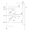
- FIG. 1 is a schematic block diagram schematically showing an electronic camera 1 as an imaging apparatus according to the first embodiment.
- the electronic camera 1 according to this embodiment is configured as a single-lens reflex digital camera, for example.
- the imaging device according to the present invention is not limited to this, and can be applied to other electronic cameras such as a compact camera, an electronic camera mounted on a mobile phone, and various imaging devices such as a film camera.
- the photographing lens 2 is attached to the electronic camera 1.
- the photographing lens 2 is driven by a lens control unit 2a for focus and diaphragm.
- the imaging surface of the solid-state imaging device 3 is arranged.
- the solid-state imaging device 3 is driven by a command from the imaging control unit 4 and outputs an image signal.
- the imaging control unit 4 controls the solid-state imaging device 3 so as to perform a horizontal pixel addition readout operation to be described later while performing a so-called rolling electronic shutter, for example.
- the imaging control unit 4 does not depend on horizontal pixel addition after exposure with a mechanical shutter (not shown) after, for example, so-called global reset that resets all pixels simultaneously.
- the solid-state imaging device 3 is controlled so as to obtain image signals of all pixels.
- Each image signal is subjected to signal processing such as black level clamping processing by the signal processing unit 5, is A / D converted by the A / D conversion unit 6, and is temporarily stored in the memory 7.
- the memory 7 is connected to the bus 8.
- the bus 8 is also connected to a lens control unit 2a, an imaging control unit 4, a CPU 9, a display unit 10 such as a liquid crystal display panel, a recording unit 11, an image compression unit 12, an image processing unit 13, and the like.
- An operation unit 9 a such as a release button is connected to the CPU 9.
- a recording medium 11a is detachably attached to the recording unit 11.
- the CPU 9 in the electronic camera 1 drives the imaging control unit 4 in accordance with the instruction of the electronic viewfinder mode or moving image shooting by the operation of the operation unit 9a.
- the imaging control unit 4 controls the solid-state imaging device 3 so as to perform a horizontal pixel addition readout operation to be described later while performing, for example, a rolling electronic shutter. At this time, the focus and the aperture are appropriately adjusted by the lens control unit 2a.
- the image signal obtained by adding the horizontal pixels obtained from the solid-state imaging device 3 is stored in the memory 7.
- the CPU 9 displays an image signal added with horizontal pixels on the display unit 10 and records the image signal added with horizontal pixels on the recording medium 11a during moving image shooting.
- the CPU 9 stores image signals not subjected to horizontal pixel addition in the memory 7 and then performs image processing as necessary based on commands from the operation unit 9a.
- the desired processing is performed by the unit 13 and the image compression unit 12, and the processed signal is output to the recording unit 11 and recorded on the recording medium 11a.
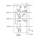
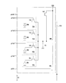
- FIG. 2 is a circuit diagram showing a schematic configuration of the solid-state imaging device 3 in FIG.
- the solid-state imaging device 3 is configured as a CMOS type solid-state imaging device, but may be configured as another XY address type solid-state imaging device.
- the solid-state imaging device 3 includes a pixel unit 21, a plurality of horizontal control signal lines 22, a vertical scanning circuit 23, a plurality of vertical signal lines V1 to Vm, and a column direction (The upper signal output circuit 24 and the lower signal output circuit 25 are arranged on both sides in the vertical direction (vertical direction in FIG. 2).
- the pixel unit 21 is arranged in a two-dimensional matrix in n rows and k columns, and an effective pixel unit 21A composed of effective pixels PX that outputs pixel signals according to incident light, and a two-dimensional matrix in n rows (m ⁇ k) columns. And an OB pixel unit 21B composed of optical black pixels (OB pixels) OB that generate black level signals.
- the OB pixel unit 21B is disposed on the right side in FIG. 2 in the row direction (horizontal direction, left-right direction in FIG. 2) of the region of the effective pixel unit 21A.
- the OB pixel unit 21B may be arranged on the left side in FIG. 2 of the effective pixel unit 21A, or may be arranged on both the left and right sides in FIG. 2 of the effective pixel unit 21A.
- a horizontal control signal line 22 connected to the vertical scanning circuit 23 is arranged in each row of the pixel unit 21.
- Each horizontal control signal line 22 supplies control signals (control signals ⁇ SEL, ⁇ RES, ⁇ TX, which will be described later) output from the vertical scanning circuit 23 to the respective rows of the pixels PX, OB.
- the plurality of vertical signal lines V1 to Vk are provided for each column of the effective pixels PX, and receive signals from the effective pixels PX in the corresponding column.
- the plurality of vertical signal lines Vk + 1 to Vm are provided for each column of the OB pixels OB, and receive signals from the OB pixels OB in the corresponding column.
- the vertical signal lines Vk + 1 to Vm are OB pixel vertical signal lines.
- the upper ends of the vertical signal lines V1 to Vm (strictly speaking, in this embodiment, the upper ends of the vertical signal lines in the even-numbered columns of these vertical signal lines) are connected to the upper signal output circuit 24. .
- the lower ends of the vertical signal lines V1 to Vm are connected to the lower signal output circuit 25.
- the vertical signal line in the first column is denoted by reference numeral V1
- the vertical signal line in the mth column is denoted by reference numeral Vm
- a constant current source 26 is connected to each of the vertical signal lines V1 to Vm (see FIGS. 5 and 6 described later).
- the constant current source 26 may be connected to the upper end side and the lower end side of each vertical signal line V1 to Vm, and two constant current sources 26 may be connected to each vertical signal line V1 to Vm. .
- the current value per constant current source is set to 1 ⁇ 2 times the current value required per vertical signal line.
- the vertical signal lines V1 to Vm are disclosed, for example, in FIGS. 4 and 5 of Japanese Patent Application Laid-Open No. 2010-263443.
- a clip circuit may be provided.
- each pixel PX on the light incident side of each pixel PX, a plurality of types of color filters that transmit light of different color components are arranged in a color array having a repetition cycle of 2 rows and 2 columns.
- the pixel PX outputs an electrical signal corresponding to each color by color separation with a color filter.
- a Bayer arrangement is adopted as the above-described color arrangement, and red (R), green (Gr, Gb), and blue (B) color filters are applied to each pixel PX according to the Bayer arrangement.
- R and Gr color filters are alternately arranged in odd rows of the effective pixel portion 21A
- Gb and B filters are alternately arranged in even rows of the effective pixel portion 21A.
- the green filter is arrange
- the effective pixel unit 21A can acquire a color image at the time of imaging.
- a color filter is arranged in the OB pixel portion 21B as well as the effective pixel portion 21A.
- the OB pixel OB outputs a black level, it is not always necessary to dispose a color filter in the OB pixel portion 21B.
- the color of the color filter is also shown in each pixel PX and OB.
- FIG. 3 is a circuit diagram showing the pixels PX and OB in FIG.
- each pixel PX includes a photodiode PD as a photoelectric conversion unit and a charge-voltage conversion unit that receives the charge and converts the charge into a voltage, similarly to a pixel of a general CMOS solid-state imaging device.
- a floating diffusion FD As a floating diffusion FD, a reset transistor RES for resetting the potential of the floating diffusion FD, a selection transistor SEL for supplying a signal corresponding to the potential of the floating diffusion FD to the vertical signal lines V1 to Vm, and a floating diffusion from the photodiode PD
- a transfer transistor TX serving as a charge transfer unit that transfers charges to the FD
- an amplification transistor AMP serving as an amplification unit that outputs the above-described signal corresponding to the potential of the floating diffusion FD are connected as shown in FIG. It has been.
- VDD is a power supply potential.
- the transistors AMP, TX, RES, and SEL of the pixels PX and OB are all nMOS transistors.
- the OB pixel OB has the same structure as the effective pixel PX except that the photodiode PD is shielded from light.
- the OB pixel OB may have a structure in which the photodiode PD is removed from the effective pixel PX, for example.
- the gates of the transfer transistors TX are commonly connected to each row, and a control signal ⁇ TX for controlling the transfer transistors TX is supplied from the vertical scanning circuit 23 to the gates.
- the gates of the reset transistors RES are commonly connected to each row, and a control signal ⁇ RES for controlling the reset transistors RES is supplied from the vertical scanning circuit 23 to the reset transistors RES.
- the gates of the selection transistors SEL are commonly connected to each row, and a control signal ⁇ SEL for controlling the selection transistors SEL is supplied from the vertical scanning circuit 23 to the selection transistors SEL.
- the photodiode PD of each pixel PX generates a signal charge according to the amount of incident light (subject light).
- the transfer transistor TX is turned on during the high level period of the control signal ⁇ TX, and transfers the charge of the photodiode PD to the floating diffusion FD.
- the reset transistor RES is turned on during the high level period (period of the power supply potential VDD) of the control signal ⁇ RES, and resets the floating diffusion FD.
- the amplification transistor AMP has its drain connected to the power supply potential VDD, its gate connected to the floating diffusion FD, its source connected to the drain of the selection transistor SEL, and a constant current source 26 (not shown in FIG. 3). 5 and FIG. 6) is configured as a source follower circuit.
- the amplification transistor AMP outputs a read signal to the vertical signal lines V1 to Vm via the selection transistor SEL according to the voltage value of the floating diffusion FD.
- the selection transistor SEL is turned on during the high level period of the control signal ⁇ SEL, and connects the source of the amplification transistor AMP to the vertical signal lines V1 to Vm.
- the vertical scanning circuit 23 in FIG. 2 receives the control signal from the imaging control unit 4 in FIG. 1 and outputs control signals ⁇ SEL, ⁇ RES, and ⁇ TX for each row of the pixels PX and OB, and the rolling electronic shutter. And a still image read operation by global reset using a mechanical shutter. Since these specific operations are known, the description thereof is omitted here.
- the configuration of the pixels PX and OB is not limited to the configuration shown in FIG.
- the configuration shown in FIG. 4 may be adopted as the configuration of the pixels PX and OB.
- FIG. 4 is a circuit diagram illustrating the pixels PX and OB according to the modification. 4, elements that are the same as or correspond to those in FIG. 3 are given the same reference numerals, and redundant descriptions thereof are omitted.
- the configuration shown in FIG. 4 is different from the configuration shown in FIG. 3 in that for each of two adjacent pixels PX and OB in the column direction, the two pixels PX and OB are a set of floating diffusion FD, amplification transistor AMP, and reset.
- the transistor RES and the selection transistor SEL are shared.
- the vertical scanning circuit 23 is configured to output control signals ⁇ SEL, ⁇ RES, ⁇ TX1, and ⁇ TX2 as shown in FIG. 4 instead of the control signals ⁇ SEL, ⁇ RES, and ⁇ TX as shown in FIG.
- the vertical scanning circuit 23 is configured to output control signals ⁇ SEL, ⁇ RES, ⁇ TX1, and ⁇ TX2 as shown in FIG. 4 instead of the control signals ⁇ SEL, ⁇ RES, and ⁇ TX as shown in FIG.
- FIG. 4 two pixels PX and OB sharing one set of floating diffusion FD, amplification transistor AMP, reset transistor RES, and selection transistor SEL are shown as a pixel block BL.
- the photodiode PD and the transfer transistor TX of the upper pixels PX and OB in the pixel block BL are denoted by reference symbols PD1, OB1 and TX1, respectively, and the photodiodes of the lower pixels PX and OB in the pixel block BL are shown.
- the diode PD and the transfer transistor TX are indicated by symbols PD2 and TX2, respectively, to distinguish them.
- control signal supplied to the gate of the transfer transistor TX1 is ⁇ TX1
- control signal supplied to the gate electrode of the transfer transistor TX2 is ⁇ TX2.
- j represents a pixel row
- j represents a row of the pixel block BL.
- One row of the pixel block BL corresponds to two rows of the pixels PX and OB.
- the vertical scanning circuit 23 receives the control signal from the imaging control unit 4 in FIG. 1 and outputs control signals ⁇ SEL, ⁇ RES, ⁇ TX1, and ⁇ TX2 for each row of the pixels PX and OB, respectively.
- control signals ⁇ SEL, ⁇ RES, ⁇ TX1, and ⁇ TX2 for each row of the pixels PX and OB, respectively.
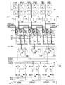
- FIG. 5 shows a part of the upper signal output circuit 24 in FIG. 2 (corresponding to the vertical signal lines V2, V4, V6 of the second column, the fourth column, and the sixth column of the effective pixel portion 21A, respectively.
- FIG. 3 is a circuit diagram showing three switch groups (each switch group is composed of switches S1 to S6) and three amplifiers CA1 to CA3).
- FIG. 6 shows three switch groups (each switch provided corresponding to each of the other parts of the upper signal output circuit 24 in FIG. 2 (the k + 2 column, the k + 4 column, and the k + 6 column of the OB pixel unit 21B).
- the group includes switches S1 to S6.) And three amplifying sections CA (k / 2) +1, CA (k / 2) +2, CA (k / 2) +3).
- FIG. 7 is a diagram showing a further part of the upper signal output circuit 24 in FIG. 2 (k / each provided corresponding to the vertical signal lines in the even-numbered columns from the second column to the k-th column of the effective pixel portion 21A.
- the output signals of the two amplifiers CA1 to CA (k / 2) and the vertical signal lines of the even-numbered columns from the (k + 2) th column to the m-th column of the OB pixel unit 21B are provided (m -K) / 2 sampling units CDS1 to CDS (m / 2), horizontal scanning circuit 31 and the like for sampling and holding the output signals of the two amplification units CA (k / 2) +1 to CA (m / 2), respectively)
- FIG. 1 The output signals of the two amplifiers CA1 to CA (k / 2) and the vertical signal lines of the even-numbered columns from the (k + 2) th column to the m-th column of the OB pixel unit 21B are provided (m -K) / 2 sampling units CDS
- the upper signal output circuit 24 is provided corresponding to each of the even-numbered vertical signal lines V2, V4,..., Vk of the effective pixel portion 21A.
- Each of the amplifiers CA1 to CA has the same configuration, and has p (three in this embodiment) input capacitors C1 to C3, an operational amplifier OP, a feedback capacitor Cf, and a column.
- a column amplifier reset switch CARST that resets the column amplifier in response to the unpreset signal ⁇ CARST.
- One end of each of the input capacitors C1 to C3 is connected to the inverting input terminal (first input terminal) of the operational amplifier OP.
- a feedback capacitor Cf and a column amplifier reset switch CARST are connected in parallel between the inverting input terminal of the operational amplifier OP and the output terminal of the operational amplifier OP.
- a predetermined potential Vref is applied to a non-inverting input terminal (second input terminal) of the operational amplifier OP.
- the column amplifier reset switch CARST is composed of a MOS transistor, and is turned on when the column amplifier reset signal ⁇ CARST is at a high level, and turned off when the column amplifier reset signal ⁇ CARST is at a low level.
- the gates of the column amplifier reset switches CARST of the amplification units CA1 to CA (k / 2) are connected in common, and a column amplifier reset signal ⁇ CARST is supplied from the imaging control unit 4 thereto.
- an operational amplifier (hereinafter referred to as an “operational amplifier with a standby function”) that can be in an operation state and an operation stop state with lower power consumption than the above-described operation state in accordance with the operation control signal ⁇ STBY. Is used).
- the entire amplification unit having the operational amplifier OP is also in the operation state and the operation stop state.
- FIG. 8 is a circuit diagram showing a specific example of an operational amplifier OP which is an operational amplifier with a standby function.
- the operational amplifier OP is composed of pMOS transistors T1 to T4 and nMOS transistors T5 to T8.
- a standby function is realized by adding transistors T3, T4, and T7 to transistors T1, T2, T5, T6, and T8 that form a general configuration of an operational amplifier.
- VIN_P, VIN_N, and VOUT indicate a non-inverting input terminal, an inverting input terminal, and an output terminal of the operational amplifier OP, respectively.
- VBIAS is a bias voltage input terminal to which a current source bias voltage from a bias circuit (not shown) is applied.
- STBY is a terminal (operation control signal input terminal) to which an operation control signal ⁇ STBY is input
- STBY_N is a terminal to which an inverted signal of the operation control signal ⁇ STBY is input.
- the operation control signal ⁇ STBY is input for each group. That is, the operation stop signal input terminals of the first group amplifiers CA1, CA4, CA7,... Are connected in common, and the operation control signal ⁇ STBY1 is supplied from the imaging control unit 4 thereto.
- the operation control signal ⁇ STBY2 is supplied from the imaging control unit 4 thereto.
- the operation stop signal input terminals of the third group amplifiers CA3, CA6, CA9,... are connected in common, and an operation control signal ⁇ STBY3 is supplied from the image pickup control unit 4 thereto.
- the switches S1 to S6 in each of the above k / 2 switch groups are composed of nMOS transistors.
- the switch S5 in each of the k / 2 switch groups described above is connected between the other end of the input capacitor C2 of the amplification unit provided corresponding to the same vertical signal line as the switch group and the vertical signal line. Turn on and off.
- the switch S5 of the switch group corresponding to the vertical signal line V4 includes the other end of the input capacitor C2 of the amplifier CA2 provided corresponding to the same vertical signal line V4 as the switch group, and the vertical signal line V4. Turn on and off.
- the switch S4 of each of the k / 2 switch groups described above corresponds to the other end of the input capacitor C1 of the amplifier provided corresponding to the same vertical signal line as the switch group and the switch group. ON / OFF between the vertical signal line two lines before the vertical signal line to be performed.
- the switch S4 of the switch group corresponding to the vertical signal line V4 corresponds to the other end of the input capacitor C1 of the amplifier CA2 provided corresponding to the same vertical signal line V4 as the switch group.
- the vertical signal line V2 that is two lines before the vertical signal line V4 is turned on / off. As shown in FIG. 5, since there is no vertical signal line to be connected when the switch S4 of the switch group corresponding to the vertical signal line V2 is on, one of the switches S4 is in a floating state.
- the switch S6 of each of the k / 2 switch groups described above corresponds to the other end of the input capacitor C3 of the amplifier provided corresponding to the same vertical signal line as the switch group, and the switch group.
- the second vertical signal line with respect to the vertical signal line to be turned on is turned on / off.
- the switch S4 of the switch group corresponding to the vertical signal line V4 corresponds to the other end of the input capacitor C3 of the amplifier CA2 provided corresponding to the same vertical signal line V4 as the switch group.
- the second vertical signal line V6 is turned on / off with respect to the vertical signal line V4.
- the switch S6 of the switch group corresponding to the vertical signal line Vk is not the vertical signal line of the effective pixel portion 21A, but is connected to the vertical signal line Vk + 2 of the OB pixel portion 21B.
- one of the switches S6 in the switch group corresponding to the vertical signal line Vk may be in a floating state without being connected to the vertical signal line Vk + 2.
- the gates of the switches S4 to S6 of the switch group corresponding to the above-mentioned first group amplifiers CA1, CA4, CA7,... Are connected in common, and a control signal ⁇ 1 is supplied from the imaging control unit 4 thereto.
- the gates of the amplification units CA2, CA5, CA8,... Of the second group are connected in common, and a control signal ⁇ 2 is supplied from the imaging control unit 4 thereto.
- the gates of the third group amplifiers CA3, CA6, CA9,... are connected in common, and a control signal ⁇ 3 is supplied from the imaging control unit 4 thereto.
- Each of the switches S4 to S6 is turned on when the control signals ⁇ 1 to ⁇ 3 supplied to its gate are at a high level (H), while the control signals ⁇ 1 to ⁇ 3 supplied to its gate are at a low level (L). Turn off.
- the switches S1 to S3 of each of the k / 2 switch groups described above are connected to the other end of the input capacitors C1 to C3 of the amplifier provided corresponding to the same vertical signal line as the switch group and the vertical switch.
- the signal line is turned on / off.
- the switches S1 to S3 of the switch group corresponding to the vertical signal line V4 are connected to the other end of the input capacitors C1 to C3 of the amplifier CA2 provided corresponding to the same vertical signal line V4 as the switch group and the vertical signal line.
- the signal line V4 is turned on / off.
- the gates of the switches S1 to S3 of the k / 2 switch group described above are connected in common, and a control signal ⁇ N is supplied from the imaging control unit 4 thereto.
- Each of the switches S1 to S3 is turned on when the control signal ⁇ N supplied to its gate is at a high level, and turned off when the control signal ⁇ N supplied to its gate is at a low level.
- the switches S4 to S6 are composed of p (three in the present embodiment) vertical signal lines and p (three in the present embodiment) input capacitance C1.
- P three in the present embodiment
- first switches that are turned on and off between C3 and C3 are configured.
- the switches S1 to S3 include p (three in this embodiment) second switches that turn on and off between only one vertical signal line and the input capacitors C1 to C3. It is composed.
- the switches S1 to S6 have p (three in the present embodiment) signals on the vertical signal lines corresponding to the control signals ⁇ 1 to ⁇ 3 and ⁇ N (three in the present embodiment).
- Switches S4 to S6 are on and switches S1 to S3 are off
- switches S1 to S3 are off
- p signals on only one vertical signal line Signal supply to be switched to a second signal supply state (switches S1 to S3 are on and switches S4 to S6 are off) that are commonly supplied to (in this embodiment, three) input capacitors C1 to C3 Part.
- FIG. 9 is a circuit diagram showing a state (the above-described second signal supply state) when any one of the amplifying units CA1 to CA (k / 2) is not added.
- FIG. 10 is a circuit diagram showing a state (the above-described first signal supply state) at the time of addition of any one of the amplifying units CA1 to CA (k / 2). 9 and 10, the line for supplying the operation control signal ⁇ STBY is omitted.
- the capacitance values of the input capacitors C1 to C3 and the feedback capacitor Cf are also denoted by the same symbols C1 to C3 and Cf, respectively.
- the switches S1 to S3 of the corresponding switch group are on and the switches S4 to S6 are off, so that the input capacitors C1 to C3 are connected in parallel as shown in FIG.
- the signal of one vertical signal line to be input is input to the input capacitors C1 to C3 connected in parallel as the input voltage Vi.
- the input voltage Vi is a signal of the vertical signal line V4.
- the inversion gain ⁇ (C1 + C2 + C3) / Cf ⁇ is obtained by the ratio of the parallel combined capacitance (C1 + C2 + C3) of the input capacitors C1 to C3 and the feedback capacitor Cf.
- an amplified output based on the change ⁇ Vi of the signal Vi of the corresponding vertical signal line, that is, a signal in a non-added state of one vertical signal line is obtained as the output signal Vout.
- the amplifying unit CA in the present embodiment the amplifying unit modified so that the input capacitors C1 to C3 are a single input capacitor and the single input capacitor is fixedly connected to a predetermined vertical signal line, This is known as a so-called column amplifier. Since the timing of the signal ⁇ CARST in this embodiment may be performed at the same timing as that of the known column amplifier, the description thereof is omitted. This is the same in the case of the state of FIG.
- the switches S4 to S6 of the corresponding switch group are on and the switches S1 to S3 are off, so that the input sides of the input capacitors C1 to C3 are electrically connected as shown in FIG.
- the signals of the corresponding three vertical signal lines are input to the input capacitors C1 to C3 as input voltages Va, Vb, and Vc, respectively.
- the amplifier CA is the amplifier CA2
- the input voltage Va is a signal on the vertical signal line V2
- the input voltage Vb is a signal on the vertical signal line V4
- the input voltage Vc is a signal on the vertical signal line V6.
- Vout is [Vref ⁇ [ ⁇ (C1 / Cf) ⁇ ⁇ Va ⁇ + ⁇ (C2 / Cf) ⁇ ⁇ Vb ⁇ + ⁇ (C3 / Cf) ⁇ ⁇ Vc ⁇ ]].
- the output voltage Vout is [Vref ⁇ ⁇ (C / Cf) ⁇ ( ⁇ Va + ⁇ Vb + ⁇ Vc) ⁇ ], and an inversion gain is obtained by adding ⁇ Va, ⁇ Vb, and ⁇ Vc without weighting. be able to.
- ⁇ Va, ⁇ Vb, and ⁇ Vc can be weighted and added using a desired weighting factor.
- the capacitance value of the input capacitor C2 to which the signal of the vertical signal line located at the center thereof is supplied is the above-mentioned p number.
- the capacitance values of the input capacitors C1 and C3 to which the signals of the vertical signal lines located in the center of the vertical signal lines are supplied are set.
- the weighting of the signal of the central vertical line signal existing at the center of gravity of the signal after the addition is made heavier than the signal of the vertical signal line at a position far from the center, the image quality after the addition can be improved.
- the present invention is not limited to this.
- the upper signal output circuit 24 is provided corresponding to the vertical signal lines Vk + 2, Vk + 4,..., Vm in the even-numbered columns of the OB pixel unit 21B.
- ⁇ (M / 2) ⁇ (k / 2) ⁇ switch groups each comprising switches S1 to S6 and ⁇ (m / 2) ⁇ (k / 2) ⁇ amplifiers CA (k / 2) +1 to CA (m / 2).
- These are for the OB pixel OB, and are provided corresponding to the vertical signal lines V2, V4,..., Vk of the even-numbered columns of the effective pixel portion 21A described with reference to FIG. .., S6, and k / 2 switch groups and k / 2 amplifiers CA1 to CA (k / 2) are configured in the same manner.
- the horizontal pixel addition and the horizontal pixel non-addition are switched for the effective pixel PX, while the OB pixel OB is always read as the horizontal pixel non-addition and signals of all columns of the OB pixel OB are read out. It is configured as follows.
- the OB pixel switch group in the OB pixel switch group, the high level is fixedly applied to the gates of the switches S1 to S3, the switches S1 to S3 are always turned on, and the low level is fixedly applied to the gates of the switches S4 to S6. Accordingly, the switches S4 to S6 are always turned off. Accordingly, the OB pixel amplification units CA (k / 2) +1 to CA (m / 2) are fixed in the non-addition state shown in FIG. In order to realize the same electrical connection state as this, the OB pixel switch group may be removed and the portions connected by the switches S1 to S3 in the on state may be connected by wiring. However, in this case, since the uniformity of the circuit is lowered and an offset or the like is likely to occur in the signal, it is preferable to provide an OB pixel switch group as in this embodiment.
- the operational control signal ⁇ STBY-OB independent of the operation control signals ⁇ STBY1 to ⁇ STBY3 is supplied to the operational amplifiers OP of the OB pixel amplification units CA (k / 2) +1 to CA (m / 2).
- the OB pixel amplifying units CA (k / 2) +1 to CA (m / 2) can be always operated independently of the amplifying units CA1 to CA (k / 2) described above.
- the upper signal output circuit 24 includes sampling units CDS1 to CDS (m / 2) provided corresponding to the amplifying units CA1 to CA (m / 2), respectively, and a horizontal scanning circuit 31. And horizontal signal lines 32N and 32S, horizontal line reset transistors RTHS and RTHN, and output amplifiers APS and APN.
- the horizontal scanning circuit 31 Under the control of the imaging control unit 4, the horizontal scanning circuit 31 outputs a horizontal scanning signal ⁇ H for each of the sampling units CDS1 to CDS (m / 2) or for each selected one, thereby performing horizontal scanning. Take control. (m / 2) attached to ⁇ H indicates a signal in the m-th column.
- Each sampling unit CDS1 to CDS (m / 2) has a first capacitor CS and a second capacitor CN.
- the first capacitor CS is a capacitor that stores optical signals and the like.
- the second capacitor CN is a capacitor for accumulating a differential signal including a noise component to be subtracted from the above-described optical signal or the like.
- Each sampling unit CDS1 to CDS (m / 2) has first and second input switches TVS and TVN and first and second output switches THS and THN.
- Each sampling unit CDS1 to CDS (m / 2) samples and holds the output signal Vout of the corresponding amplifying unit CA1 to CA (m / 2) according to the control signals ⁇ TVN and ⁇ TVS, and horizontally holds the held signal.
- the horizontal signal lines 32N and 32S are supplied.
- the optical signal and the like and the difference signal output to the horizontal signal lines 32N and 32S are amplified through the output amplifiers APS and APN, respectively, and output to the signal processing unit 5 in FIG.
- the signal processing unit 5 obtains the difference between the outputs of the output amplifiers APS and APN using a differential amplifier or the like. Thereby, correlated double sampling is realized.
- sampling units CDS1 to CDS (m / 2) are provided to remove the offset of the amplification units CA1 to CA (m / 2).
- the horizontal line reset transistors RTHS and RTHN reset the horizontal signal lines 32S and 32N to a predetermined potential Vref0 at a predetermined timing in accordance with the horizontal line reset control signal ⁇ RTH.
- sampling units CDS1 to CDS (m / 2) themselves are known, a detailed description thereof will be omitted.
- the lower signal output circuit 25 in FIG. 2 is a circuit obtained by vertically inverting the upper signal output circuit 24.
- the portions connected to the even-numbered vertical signal lines V 2, V 4,..., Vm in the upper signal output circuit 24 are the odd-numbered vertical signal lines in the pixel unit 21.
- Vm ⁇ 1 are connected to V1, V3,.
- the signal output circuit is divided into the upper signal output circuit 24 and the lower signal output circuit 25 as described above, the space can be used effectively, and both processes are performed in parallel. This can increase the processing speed.
- the signal output circuit may be arranged only on either the upper side or the lower side.
- an operation mode (hereinafter referred to as “horizontal pixel non-addition readout mode”) in which signals of all pixels PX are read out without horizontal pixel addition during normal main shooting (still image shooting) or the like is performed. Is called.
- FIG. 11 is an operation explanatory diagram schematically showing a characteristic operation of the horizontal pixel non-addition readout mode of the solid-state imaging device 3 shown in FIG.
- FIG. 12 is a timing chart showing the state of the control signal in the horizontal pixel non-addition readout mode of the solid-state imaging device 3 shown in FIG.
- the upper and lower control signals ⁇ N (of the upper signal output circuit 24 and the lower signal output circuit 25) are maintained at a high level, while the upper and Lower control signals ⁇ 1, ⁇ 2, and ⁇ 3 are maintained at a low level. Therefore, the upper and lower effective pixel amplifying units CA1 to CA (k / 2) are all maintained in the non-addition state shown in FIG.
- the upper and lower OB pixel amplifying units CA (k / 2) +1 to CA (m / 2) are originally fixed in the non-addition state shown in FIG.
- the vertical signal lines V2, V4,..., Vm in the even-numbered columns are connected to the upper amplification units CA1 to CA (m / 2) in FIG. It is connected to the input section in the non-addition state shown.
- the odd-numbered vertical signal lines V1, V3,..., Vm ⁇ 1 are connected to the lower amplification units CA1 to CA (m / 2). 9 are connected to the non-addition state input units shown in FIG.
- the upper and lower operation control signals ⁇ STBY1 to ⁇ STBY3 and ⁇ STBY-OB are maintained at a low level, and all the upper and lower amplification units CA1 to CA1- CA (m / 2) is maintained in the operating state.
- the vertical scanning circuit 23 sequentially selects one row at a time from the first row to the n-th row under the control of the imaging control unit 4, and each pixel PX in the row to be read , OB are output to the vertical signal lines V1 to Vm of the corresponding column.
- the vertical signal lines V2, V4,..., Vm in the even-numbered columns are provided with Gr pixels (Gr color filters provided in the corresponding columns).
- the signals of the effective pixels PX and OB pixels OB) are output, and the signals of the R pixels of the corresponding columns are output to the vertical signal lines V1, V3,.
- the Gr pixel signals output to the even-numbered vertical signal lines V2, V4,..., Vm are in the non-adding state and the operating state of the upper amplifiers CA1 to CA (m / 2), and after being sampled by the upper sampling units CDS1 to CDS (m / 2), all the sampled Gr pixel signals are sequentially output by the upper horizontal scanning circuit 31 to output amplifiers APS, APN. Is output from.
- the R pixel signals output to the odd-numbered vertical signal lines V1, V3,..., Vm ⁇ 1 are in the non-addition state and the operation state of the lower amplification units CA1 to CA shown in FIG.
- the signals of the B pixels in the corresponding column are output to the vertical signal lines V2, V4,.
- the signals of the Gb pixels in the corresponding column are output to the odd-numbered vertical signal lines V1, V3,.
- the B pixel signals output to the vertical signal lines V2, V4,..., Vm in the even-numbered columns are in the non-addition state shown in FIG. 2), and after being sampled by the upper sampling units CDS1 to CDS (m / 2), all the sampled B pixel signals are sequentially output by the upper horizontal scanning circuit 31 to output amplifiers APS and APN. Is output from.
- the Gb pixel signals output to the odd-numbered vertical signal lines V1, V3,..., Vm ⁇ 1 are in the non-addition state and the operation state of the lower amplification units CA1 to CA shown in FIG. After being amplified by (m / 2), after being sampled by the lower sampling units CDS1 to CDS (m / 2), the signals of all the sampled Gb pixels are sequentially transmitted by the lower horizontal scanning circuit 31. Output from the output amplifiers APS and APN.
- an operation mode (hereinafter referred to as “horizontal pixel addition readout mode”) in which the signal of the effective pixel PX is read by adding the horizontal pixel is performed in the electronic viewfinder mode or the moving image shooting mode.
- FIG. 13 is an operation explanatory diagram schematically showing a characteristic operation of the horizontal pixel addition readout mode of the solid-state imaging device 3 shown in FIG.
- FIG. 14 is a timing chart showing the state of the control signal in the horizontal pixel addition readout mode of the solid-state imaging device 3 shown in FIG.
- the upper and lower control signals ⁇ N are maintained at a low level. Accordingly, the upper and lower effective pixel amplification units CA1 to CA (k / 2) are all maintained in the addition state shown in FIG.
- the upper and lower OB pixel amplifying units CA (k / 2) +1 to CA (m / 2) are originally fixed in the non-addition state shown in FIG.
- the upper control signal ⁇ 2 is maintained at a high level, and the upper control signals ⁇ 1 and ⁇ 3 are maintained at a low level. Accordingly, the upper effective pixel amplifiers CA2, CA5, CA8, The signals of the vertical signal lines to be added are determined, and for example, the signals of the vertical signal lines V2, V4, V6 are added in the upper effective pixel amplifier CA2.
- the lower control signal ⁇ 1 is maintained at a high level, and the lower control signals ⁇ 2, ⁇ 3 are maintained at a low level.
- the signals of the vertical signal lines to be added are determined. For example, the signals of the vertical signal lines V5, V7, and V9 are added in the lower effective pixel amplifier CA4.
- the upper control signals ⁇ STBY2, ⁇ STBY-OB are maintained at a low level, and the upper ⁇ STBY1, ⁇ STBY3 are maintained at a high level. Therefore, in the upper signal output circuit 24, only the effective pixel amplification units CA2, CA5, CA8,... Are maintained in the active state with respect to the effective pixel unit 21A, and the remaining effective pixel amplification units CA1, CA3, CA4, and CA6. , CA7, CA9,... Are kept in a stopped state.
- the upper OB pixel amplification units CA (k / 2) +1 to CA (m / 2) are maintained in the operating state.
- the lower control signals ⁇ STBY1, ⁇ STBY-OB are maintained at a low level, and the lower ⁇ STBY2, ⁇ STBY3 are maintained at a high level. Therefore, in the lower signal output circuit 25, only the effective pixel amplifiers CA1, CA4, CA7,... Are maintained in the active state with respect to the effective pixel unit 21A, and the remaining effective pixel amplifiers CA2, CA3, CA5,. CA6, CA8, CA9,... Are maintained in a stopped state.
- the lower OB pixel amplifier CA (k / 2) +1 to CA (m / 2) is maintained in the operating state.
- the vertical scanning circuit 23 sequentially selects one row at a time from the first row to the n-th row under the control of the imaging control unit 4, and each pixel PX, The OB signal is output to the vertical signal lines V1 to Vm in the corresponding column.
- the vertical signal lines V2, V4,..., Vm in the even-numbered columns are provided with Gr pixels (Gr color filters provided in the corresponding columns).
- the signals of the effective pixels PX and OB pixels OB) are output, and the signals of the R pixels of the corresponding columns are output to the vertical signal lines V1, V3,.
- the Gr pixel signals output to the vertical signal lines V2, V4,..., Vk of the even columns are in the addition state shown in FIG.
- the signals of three Gr pixels that do not overlap each other are added by CA8,.
- the intervals in the row direction between the gravity center positions of the Gr pixels after the addition are equal pitches.
- the Gr pixel signals output to the vertical signal lines Vk + 2,..., Vm in the even-numbered columns are in the non-addition state shown in FIG. 9 and the upper OB pixel CA (k / 2) +1 in the operating state. Amplified by ⁇ CA (m / 2).
- the output signals of the upper amplifying sections CA1 to CA (m / 2) including these significant signals are sampled by the upper sampling sections CDS1 to CDS (m / 2), and then the sampled signals are The signals are sequentially output from the output amplifiers APS and APN by the horizontal scanning circuit 31.
- the upper horizontal scanning circuit 31 may output all the sampled signals (read all columns), or output from the upper effective pixel amplifiers CA2, CA5, CA8,. Only the signal (addition signal of Gr pixel) and the output signal (addition signal of Gr pixel) of the upper OB pixel CA (k / 2) +1 to CA (m / 2) are selectively output (column selection read). You may do it. In the former case, unnecessary signals need not be used in the subsequent circuit.
- the R pixel signals output to the odd-numbered vertical signal lines V1, V3,..., Vk ⁇ 1 are in the addition state shown in FIG. , CA4, CA7,..., Add three R pixel signals that do not overlap each other.
- the intervals in the row direction between the centroid positions of the R pixels after addition are equal pitches, and the centroid positions of the signals of the R pixels after addition and the Gr pixels after addition described above.
- the interval between the signal and the center of gravity of the signal is also equal.
- the R pixel signals output to the odd-numbered vertical signal lines Vk + 1,..., Vm ⁇ 1 are in the non-addition state shown in FIG. 2) Amplified by +1 to CA (m / 2).
- the output signals of the lower amplification units CA1 to CA (m / 2) including these significant signals are sampled by the lower sampling units CDS1 to CDS (m / 2), and then the sampled signals are The signals are sequentially output from the output amplifiers APS and APN by the lower horizontal scanning circuit 31.
- the lower horizontal scanning circuit 31 may output all the sampled signals (read all columns), or lower effective pixel amplification units CA1, CA4, CA7,...
- Output signal (R pixel addition signal) and lower OB pixel CA (k / 2) +1 to CA (m / 2) output signals (R pixel addition signal) are selectively output (columns). (Selective reading). In the former case, unnecessary signals need not be used in the subsequent circuit.
- the signals of the B pixels in the corresponding column are output to the vertical signal lines V2, V4,.
- the signals of the Gb pixels in the corresponding column are output to the odd-numbered vertical signal lines V1, V3,.
- the B pixel signals output to the vertical signal lines V2, V4,..., Vk in the even columns are in the addition state shown in FIG.
- CA8 Signals of three B pixels that do not overlap each other are added.
- the intervals in the row direction between the barycentric positions of the B pixels after addition are equal pitches.
- the B pixel signals output to the vertical signal lines Vk + 2,..., Vm in the even-numbered columns are in the non-addition state shown in FIG. 9 and the upper OB pixel CA (k / 2) +1 in the operating state. Amplified by ⁇ CA (m / 2).
- the output signals of the upper amplifying sections CA1 to CA (m / 2) including these significant signals are sampled by the upper sampling sections CDS1 to CDS (m / 2), and then the sampled signals are The signals are sequentially output from the output amplifiers APS and APN by the horizontal scanning circuit 31.
- the upper horizontal scanning circuit 31 may output all the sampled signals (read all columns), or output from the upper effective pixel amplifiers CA2, CA5, CA8,. Only the signal (addition signal of Gr pixel) and the output signal (addition signal of B pixel) of CA (k / 2) +1 to CA (m / 2) for the upper OB pixel are selectively output (column selection readout). You may do it. In the former case, unnecessary signals need not be used in the subsequent circuit.
- the Gb pixel signals output to the odd-numbered vertical signal lines V1, V3,..., Vk ⁇ 1 are in the addition state shown in FIG. , CA4, CA7,..., Three Gb pixel signals that do not overlap each other are added.
- the intervals in the row direction between the centroid positions of the Gb pixels after the addition are equal pitches, and the centroid positions of the signals of the Gb pixels after the addition and the B pixels after the addition described above.
- the interval between the signal and the center of gravity of the signal is also equal.
- the Gb pixel signals output to the odd-numbered vertical signal lines Vk + 1,..., Vm ⁇ 1 are in the non-addition state shown in FIG. 2) Amplified by +1 to CA (m / 2).
- the output signals of the lower amplification units CA1 to CA (m / 2) including these significant signals are sampled by the lower sampling units CDS1 to CDS (m / 2), and then the sampled signals are The signals are sequentially output from the output amplifiers APS and APN by the lower horizontal scanning circuit 31.
- the lower horizontal scanning circuit 31 may output all the sampled signals (read all columns), or lower effective pixel amplification units CA1, CA4, CA7,... Output signal (Gb pixel addition signal) and the lower OB pixel CA (k / 2) +1 to CA (m / 2) output signals (Gb pixel addition signal) are selectively output (columns). (Selective reading). In the former case, unnecessary signals need not be used in the subsequent circuit.
- the signals of the effective pixels PX can be read by horizontal addition, while the signals of all the OB pixels OB can be read without adding the horizontal pixels.
- the vertical scanning circuit 23 reads out one row at a time. However, reading may be performed every three rows and thinned out in the vertical direction.
- the solid-state imaging device 3 may be configured so that pixels in the vertical direction can be added, and pixel addition reading can be performed in the vertical direction as well. These points are the same in the second embodiment described later.
- the amplifying units C1 to Ck have not only an amplification function but also a horizontal pixel addition function (addition state function shown in FIG. 10), a dedicated addition circuit for adding horizontal pixel signals.
- the pixel signals in the horizontal direction can be added without using.
- the amplification units (upper effective pixel amplification units CA1, CA3, CA4, CA6, CA7, CA9,.
- the effective pixel amplifiers CA2, CA3, CA5, CA6, CA8, CA9,...) are maintained in the operation stop state with low power consumption, so that the power consumption can be reduced.
- the intervals in the row direction between the barycentric positions of the pixels of each color after addition are equal pitches, and the barycenters of the pixels of different colors after addition.
- the intervals between the positions in the row direction are equal pitches. Therefore, according to the present embodiment, moire and false colors are unlikely to occur.
- the horizontal pixel addition readout mode described above may be modified as follows. That is, the upper and lower control signals ⁇ N are maintained at a low level, the upper and lower control signals ⁇ 1 to ⁇ 3 are maintained at a high level, and the upper and lower control signals ⁇ STBY1 to ⁇ STBY3 and ⁇ STBY-OB are set to a low level. You may maintain the level.
- signals from pixels in p columns (three columns in this example) provided with color filters of the same color and adjacent in the row direction in the p columns (three columns in this example) are the upper and lower effective pixel amplification units CA1 to CA (k / 2). Obtained from each.
- the upper and lower horizontal scanning circuits 31 read out all the output signals of the sampled upper and lower effective pixel amplifiers CA1 to CA (k / 2).
- FIG. 15 is a circuit diagram showing a part of the upper signal output circuit 24 of the solid-state imaging device used in the electronic camera according to the second embodiment, and corresponds to FIG.
- FIG. 16 is a circuit diagram showing another part of the upper signal output circuit 24 of the solid-state imaging device used in the electronic camera according to the second embodiment, and corresponds to FIG. 15 and 16, the same or corresponding elements as those in FIGS. 5 and 6 are denoted by the same reference numerals, and redundant description thereof is omitted.
- the upper signal output circuit 24 corresponds to m / 2 amplifying units CA1 to CA (m / 2), respectively, and corresponds to m / 2 switch groups each including switches S1 to S6.
- m / 2 vertical line selection switch group line selection unit, each consisting of switches S7 to S9, is added.
- the switches S7 to S9 of each vertical line selection switch group are connected to the vertical signal lines V2, V4,..., Vm of even columns in the upper signal output circuit 24 in the first embodiment described above.
- the vertical signal line is provided so as to be selectively connected to any one of the vertical signal line, the vertical signal line immediately before the vertical signal line, and the vertical signal line after the vertical signal line.
- the switches S7 to S9 of the vertical line selection switch group corresponding to the amplifier CA1 are connected to the vertical signal line V2 in the upper signal output circuit 24 in the first embodiment described above. Are connected to any one of the vertical signal line V2, the vertical signal line V1 immediately before the vertical signal line V2, and the vertical signal line V4 after the vertical signal line V2. It has been.
- the switch S7 of the switches S7 to S9 of the vertical line selection switch group is selectively turned on, the location connected to the vertical signal line V2 in the upper signal output circuit 24 in the first embodiment described above is selected. Are selectively connected to the vertical signal line V1 on the first column side.
- the switch S8 of the switches S7 to S9 of this vertical line selection switch group When the switch S8 of the switches S7 to S9 of this vertical line selection switch group is selectively turned on, the location connected to the vertical signal line V2 in the upper signal output circuit 24 in the first embodiment described above is selected.
- the second is selectively connected to the vertical signal line V2 on the second column side.
- the switch S9 of the switches S7 to S9 of this vertical line selection switch group is selectively turned on, the location connected to the vertical signal line V2 in the upper signal output circuit 24 in the first embodiment described above is selected.
- the third is selectively connected to the vertical signal line V4 on the third column side.
- the switches S7 to S9 of the vertical line selection switch group corresponding to the amplification unit CA2 in the upper signal output circuit 24 are connected to the vertical signal line V4 in the upper signal output circuit 24 in the first embodiment described above. So as to be selectively connected to any one of the vertical signal line V4, the vertical signal line V3 immediately preceding the vertical signal line V4, and the vertical signal line V6 subsequent to the vertical signal line V4. Is provided.
- the switch S7 of the switches S7 to S9 of the vertical line selection switch group is selectively turned on, the location connected to the vertical signal line V4 in the upper signal output circuit 24 in the first embodiment described above is selected. Are selectively connected to the vertical signal line V3 on the first column side.
- the switches S7 to S9 in each of the above-mentioned m / 2 vertical line selection switch groups are composed of nMOS transistors.
- a switch S7 of each vertical line selection switch group is connected in common, and a control signal ⁇ SEL7 is supplied from the imaging control unit 4 thereto.
- a switch S8 of each vertical line selection switch group is connected in common, and a control signal ⁇ SEL8 is supplied from the imaging control unit 4 thereto.
- a switch S9 of each vertical line selection switch group is connected in common, and a control signal ⁇ SEL9 is supplied from the imaging control unit 4 thereto.
- Each of the switches S7 to S8 is turned on when the control signals ⁇ SEL7 to ⁇ SEL9 supplied to its gate are at a high level, and turned off when the control signals ⁇ SEL7 to ⁇ SEL9 supplied to its gate are at a low level.
- the lower signal output circuit 25 is a circuit obtained by simply inverting the upper signal output circuit 24 described above.
- an operation mode (hereinafter referred to as “horizontal pixel non-addition readout mode”) in which signals of all the pixels PX are read out without horizontal pixel addition during normal main shooting (still image shooting) or the like. Done.
- FIG. 17 is an operation explanatory view schematically showing a characteristic operation of the horizontal pixel non-addition readout mode of the solid-state imaging device 3 in the present embodiment, and corresponds to FIG.
- FIG. 18 is a timing chart showing the state of the control signal in the horizontal pixel non-addition readout mode of the solid-state imaging device 3 in the present embodiment, and corresponds to FIG.
- the upper and lower control signals ⁇ SEL9 are maintained at a low level, and when the odd-numbered row is to be read, the upper control signal ⁇ SEL7 is set to a low level.
- the lower control signal ⁇ SEL7 is set to the high level and the upper control signal ⁇ SEL8 is set to the high level while the lower control signal ⁇ SEL8 is set to the low level, the even-numbered rows are to be read.
- the upper control signal ⁇ SEL7 is set to high level while the lower control signal ⁇ SEL7 is set to low level, and the upper control signal ⁇ SEL8 is set to low level while the lower control signal ⁇ SEL8 is set to high level.
- an operation mode (hereinafter referred to as “horizontal pixel addition reading mode”) in which the signal of the effective pixel PX is read by adding the horizontal pixel is performed in the electronic viewfinder mode or moving image shooting.
- FIG. 19 is an operation explanatory diagram schematically showing a characteristic operation of the horizontal pixel addition reading mode of the solid-state imaging device 3 in the present embodiment, and corresponds to FIG.
- FIG. 20 is a timing chart showing the state of the control signal in the horizontal pixel addition readout mode of the solid-state imaging device 3 in the present embodiment, and corresponds to FIG.
- the upper and lower control signals ⁇ N are maintained at a low level
- the upper and lower control signals ⁇ 1 are maintained at a high level
- the upper and lower control signals ⁇ N are maintained.
- Lower control signals ⁇ 2 and ⁇ 3 are maintained at low level
- upper and lower control signals ⁇ STBY1 and ⁇ STBY-OB are maintained at low level
- upper and lower ⁇ STBY2 and ⁇ STBY3 are maintained at high level.
- the upper and lower control signals ⁇ SEL8 are maintained at the low level and the odd-numbered row is the readout target
- the upper side The control signal ⁇ SEL7 is set to low level while the lower control signal ⁇ SEL7 is set to high level
- the upper control signal ⁇ SEL9 is set to high level while the lower control signal ⁇ SEL9 is set to low level.
- the upper control signal ⁇ SEL7 is set to the high level while the lower control signal ⁇ SEL7 is set to the low level
- the upper control signal ⁇ SEL9 is set to the low level while the lower control signal ⁇ SEL7 is set to the low level.
- the control signal ⁇ SEL9 is set to the high level.
- the upper control signal ⁇ SEL8 is maintained at a high level
- the upper control signals ⁇ SEL7 and ⁇ SEL9 are maintained at a low level
- the lower control signal ⁇ SEL7 is maintained at a high level
- the upper control signal By maintaining ⁇ SEL8 and ⁇ SEL9 at a low level, the solid-state imaging device 3 in the present embodiment is in exactly the same connection state as the solid-state imaging device 3 in the first embodiment described above. Therefore, also in this embodiment, the horizontal pixel non-addition readout mode and the horizontal pixel addition readout mode in the first embodiment described above can be realized by maintaining such a connection state.
- FIG. 21 is a block diagram illustrating a configuration example of the solid-state imaging device according to the third embodiment.
- the solid-state imaging device according to the third embodiment is an XY address type solid-state imaging device formed on a silicon substrate using a CMOS (complementary metal oxide semiconductor) process.
- the solid-state imaging device of the third embodiment is mounted on an imaging device such as a digital still camera or a video camera (a configuration example of the imaging device will be described later).
- the solid-state imaging device of the third embodiment has an operation mode (normal readout mode) for reading out electrical signals of each pixel independently, and an operation mode (mixed readout mode) for reading out electrical signals mixed from a plurality of pixels.
- an operation mode normal readout mode
- an operation mode mixed readout mode
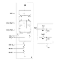
- the solid-state imaging device 111 includes a pixel array 112, a plurality of horizontal control signal lines 113, a vertical scanning circuit 114, a plurality of vertical signal lines 115, a first signal output circuit 116, a second signal output circuit 117, And an image sensor control circuit 118.
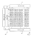
- the pixel array 112 has a plurality of pixels PX that convert incident light into electrical signals.
- the pixels PX of the pixel array 112 are arranged in a matrix in the first direction D1 and the second direction D2 on the light receiving surface.
- the first direction D1 and the second direction D2 are also referred to as a row direction D1 and a column direction D2, respectively.
- the arrangement of the pixels PX is simplified, but it goes without saying that a larger number of pixels are arranged on the light receiving surface of the actual solid-state imaging device.
- each pixel PX On the front surface of each pixel PX, a plurality of types of color filters that transmit light of different color components are arranged in a predetermined color arrangement. Therefore, the pixel PX outputs an electrical signal corresponding to each color by color separation with a color filter.
- red (R), green (Gr, Gb), and blue (B) color filters are arranged in each pixel PX according to a 2-by-2 Bayer array. Thereby, the pixel array 112 can acquire a color image at the time of imaging.
- the pixels PX having red (R), green (Gr, Gb), and blue (B) filters are also referred to as red pixels (R), blue pixels (B), and green pixels (Gr, Gb), respectively.
- red pixels (R) and green pixels (Gr) are alternately arranged in odd rows of the pixel array 112. Further, for example, in even rows of the pixel array 112, green pixels (Gb) and blue pixels (B) are alternately arranged.
- green pixels (Gb) and red pixels (R) are alternately arranged.
- blue pixels (B) and green pixels (Gr) are alternately arranged.
- Each horizontal control signal line 113 supplies control signals (a selection signal ⁇ SEL, a reset signal ⁇ RST, and a transfer signal ⁇ TX, which will be described later) output from the vertical scanning circuit 114 to the pixel groups arranged in the row direction D1.
- control signals a selection signal ⁇ SEL, a reset signal ⁇ RST, and a transfer signal ⁇ TX, which will be described later
- each column of the pixel array 112 vertical signal lines 115 that are examples of signal readout lines are arranged.
- the plurality of pixels PX arranged in the column direction D2 are connected to each other by a vertical signal line 115 provided for each column. That is, the pixel array 112 outputs output signals from a plurality of pixels PX arranged in the same column via a common vertical signal line 115.
- the odd-numbered vertical signal lines 115 corresponding to the green pixel (Gb) and the red pixel (R) are connected to the first signal output circuit 116 located on the lower side of FIG.
- the even-numbered vertical signal lines 115 corresponding to the blue pixel (B) and the green pixel (Gr) are respectively connected to the second signal output circuit 17 located on the upper side of FIG.
- the pixel PX includes a photodiode PD, a transfer transistor TX, a reset transistor RST, an amplification transistor AMP, a selection transistor SEL, and a floating diffusion FD.
- the photodiode PD generates a signal charge by photoelectric conversion according to the amount of incident light.
- the transfer transistor TX is turned on during the high level period of the transfer signal ⁇ TX, and transfers the signal charge accumulated in the photodiode PD to the floating diffusion FD.
- the source of the transfer transistor TX is a photodiode PD, and the drain of the transfer transistor TX is a floating diffusion FD.
- the floating diffusion FD is a diffusion region formed by introducing impurities into a semiconductor substrate, for example.
- the floating diffusion FD is connected to the gate of the amplification transistor AMP and the source of the reset transistor RST.
- the reset transistor RST is turned on during the high level period of the reset signal ⁇ RST, and resets the floating diffusion FD to the power supply voltage VDD.
- the amplification transistor AMP has a drain connected to the power supply voltage VDD, a gate connected to the floating diffusion FD, a source connected to the drain of the selection transistor SEL, and a constant current source connected to the vertical signal line 115.
- a source follower circuit having a load 119 (not shown in FIG. 21) is configured.
- the amplification transistor AMP outputs a read voltage via the selection transistor SEL according to the voltage value of the floating diffusion FD.
- the selection transistor SEL is turned on during a high level period of the selection signal ⁇ SEL, and connects the source of the amplification transistor AMP to the vertical signal line 115.
- Each vertical signal line 115 is connected to a clip circuit 120 (not shown in FIG. 21) for clipping the voltage of the vertical signal line 115 to a predetermined value.
- the clipping circuit 120 includes a transistor MCL1 that generates a clipping voltage and a transistor MCL2 that controls ON / OFF of clipping.
- the clip circuit 120 is formed by cascode-connecting the transistors MCL1 and MCL2, connecting the drain of the transistor MCL1 to the power supply voltage VDD, and connecting the source of the transistor MCL2 to the vertical signal line 115.
- the first signal output circuit 116 and the second signal output circuit 117 are arranged in parallel up and down across the pixel array 112.
- the first signal output circuit 116 is a circuit that is arranged on the lower side of FIG. 21 and reads out the image signals (Gb or R) of the odd columns of the pixel array 112 for each color in the row direction D1.
- the second signal output circuit 117 is arranged on the upper side of FIG. 21 and reads out the image signals (B or Gr) of the even-numbered columns of the pixel array 112 for each color in the row direction D1.
- the image signal can be read from the pixel array 112 at high speed.
- first signal output circuit 116 and the second signal output circuit 117 are arranged in the crossing direction (row direction D1) with respect to the extending direction of the vertical signal line 115 (column direction D2) in the mixed readout mode.
- Image signals are mixed and read from the plurality of pixels PX.
- the first signal output circuit 116 and the second signal output circuit 117 in the third embodiment read out signals for three pixels of the same color in the row direction D1 in the mixed readout mode (details of the mixed readout). Will be described later).
- the image sensor control circuit 118 supplies control signals to the vertical scanning circuit 114, the first signal output circuit 116, and the second signal output circuit 117, respectively.
- control signal described above may be supplied from a control unit of an imaging apparatus on which the solid-state imaging device of the third embodiment is mounted.
- the image sensor control circuit 118 can be omitted from the solid-state image sensor 111.
- the configuration example of the first signal output circuit 116 and the second signal output circuit 117 will be described in more detail with reference to FIG.
- the second signal output circuit 117 has the same basic configuration as the first signal output circuit 116 except that the even-numbered vertical signal lines 115 are connected. Therefore, in the following example, an example of the first signal output circuit 116 will be shown, and any redundant description regarding the second signal output circuit 117 will be omitted.
- the first signal output circuit 116 includes a mixed readout control unit 121, a column amplifier 122, a sample hold unit 123, and a horizontal scanning circuit 124.
- One set of each of the mixed readout control unit 121, the column amplifier 122, and the sample hold unit 123 is provided for one vertical signal line 115. Further, only one horizontal scanning circuit 124 is provided in the first signal output circuit 116.
- the element corresponding to the 3m-2nd (eg, 1, 4, 7th) of the odd-numbered column is suffixed with the symbol a, and the odd-numbered column of 3m-1
- the element corresponding to the th (for example, 2, 5 and 8th) is suffixed with b, and the element corresponding to the 3mth (for example, 3, 6, 9th) of the odd column is suffixed with c.
- m is a natural number excluding 0).
- the mixed readout control units 121a to 121c are circuits that switch on / off the mixed readout of the pixel PX. For example, in the normal reading mode, the mixed reading control unit 121 reads the output signal of the pixel PX from only a predetermined odd number column of the pixel array 112. On the other hand, in the mixed readout mode, the mixed readout control unit 121 mixes and reads output signals from pixels PX for three columns adjacent in the row direction D1 among the odd columns of the pixel array 112.
- the mixed readout control unit 121a is connected to the mode selection signal line ⁇ N and the phase selection signal line ⁇ 1.
- the mixed readout control unit 121b is connected to the mode selection signal line ⁇ N and the phase selection signal line ⁇ 2.
- the mixed readout control unit 121c is connected to the mode selection signal line ⁇ N and the phase selection signal line ⁇ 3. Then, the mixed read controllers 121a to 121c in the mixed read mode operate independently in response to the phase selection signals ⁇ 1 to ⁇ 3.
- the first mixed readout control unit 121a corresponding to the 3m-2th column described above includes transistors Ma1 to Ma6 and capacitors Ca1 to Ca3.
- the transistors Ma1 to Ma3, the transistors Ma4 to Ma6, and the capacitors Ca1 to Ca3 are arranged in parallel, three by three.
- the gates of the transistors Ma1 to Ma3 are all connected to a common mode selection signal line ⁇ N that instructs mode switching.
- the sources of the transistors Ma1 to Ma3 are all connected to the vertical signal line 115 corresponding to the 3m-2nd column of the odd number column.
- the gates of the transistors Ma4 to Ma6 are all connected to the phase selection signal line ⁇ 1.
- the source of the transistor Ma4 is connected to the vertical signal line 115 corresponding to the adjacent 3m-th column.
- the source of the transistor Ma5 is connected to the vertical signal line 115 corresponding to the 3m-2nd column.
- the source of the transistor Ma6 is connected to the vertical signal line 115 corresponding to the adjacent 3m ⁇ 1th column.
- the drains of the transistors Ma1 and Ma4 are all connected to the capacitor Ca1
- the drains of the transistors Ma2 and Ma5 are both connected to the capacitor Ca2
- the drains of the transistors Ma3 and Ma6 are all connected to the capacitor Ca3.
- These capacitors Ca1 to Ca3 are connected to the first column amplifier 122a in the subsequent stage and serve as the input capacitance of the first column amplifier 122a.
- the second mixed readout control unit 121b corresponding to the above-mentioned 3m-1th column has transistors Mb1 to Mb6 and capacitors Cb1 to Cb3.
- the transistors Mb1 to Mb3, the transistors Mb4 to Mb6, and the capacitors Cb1 to Cb3 are each arranged in parallel.
- the gates of the transistors Mb1 to Mb3 are all connected to the common mode selection signal line ⁇ N described above.
- the sources of the transistors Mb1 to Mb3 are all connected to the vertical signal line 115 corresponding to the 3m-1st column of the odd columns.
- the gates of the transistors Mb4 to Mb6 are all connected to the phase selection signal line ⁇ 2.
- the source of the transistor Mb4 is connected to the vertical signal line 115 corresponding to the adjacent 3m-2nd column.
- the source of the transistor Mb5 is connected to the vertical signal line 115 corresponding to the 3m-1st column.
- the source of the transistor Mb6 is connected to the vertical signal line 115 corresponding to the adjacent 3m-th column.
- the drains of the transistors Mb1 and Mb4 are all connected to the capacitor Cb1, the drains of the transistors Mb2 and Mb5 are both connected to the capacitor Cb2, and the drains of the transistors Mb3 and Mb6 are all connected to the capacitor Cb3.
- These capacitors Cb1 to Cb3 are connected to the second column amplifier 122b in the subsequent stage, and become the input capacitors of the second column amplifier 122b.
- the third mixed readout control unit 121c corresponding to the 3m-th column includes transistors Mc1 to Mc6 and capacitors Cc1 to Cc3.
- the transistors Mc1 to Mc3, the transistors Mc4 to Mc6, and the capacitors Cc1 to Cc3 are each arranged in parallel.
- the gates of the transistors Mc1 to Mc3 are all connected to the common mode selection signal line ⁇ N described above.
- Each source of the transistors Mc1 to Mc3 is connected to the vertical signal line 115 corresponding to the 3m-th column of the odd-numbered column.
- the gates of the transistors Mc4 to Mc6 are all connected to the phase selection signal line ⁇ 3.
- the source of the transistor Mc4 is connected to the vertical signal line 115 corresponding to the adjacent 3m-1th column.
- the source of the transistor Mc5 is connected to the vertical signal line 115 corresponding to the 3m-th column.
- the source of the transistor Mc6 is connected to the vertical signal line 115 corresponding to the adjacent 3m-2nd column.
- the drains of the transistors Mc1 and Mc4 are all connected to the capacitor Cc1
- the drains of the transistors Mc2 and Mc5 are both connected to the capacitor Cc2
- the drains of the transistors Mc3 and Mc6 are all connected to the capacitor Cc3.
- These capacitors Cc1 to Cc3 are connected to the third column amplifier 122c at the subsequent stage and serve as the input capacitors of the third column amplifier 122c.
- the column amplifier 122 is an inverting amplifier having, for example, an operational amplifier OP which is an example of an amplifying unit, a feedback capacitor Cf, and a control switch Sf, and outputs an output signal output from the pixel PX via the vertical signal line 115. Invert amplification for each column.
- an operational amplifier OP which is an example of an amplifying unit, a feedback capacitor Cf, and a control switch Sf, and outputs an output signal output from the pixel PX via the vertical signal line 115. Invert amplification for each column.
- a constant potential Vref_PGA is supplied to the non-inverting input terminal of the operational amplifier OP.
- the inverting input terminal of the operational amplifier OP is connected to the input capacitance of the mixed readout control unit 121.
- each of the feedback capacitor Cf and the control switch Sf has one end connected to the output terminal of the operational amplifier OP and the other end connected to the inverting input terminal of the operational amplifier OP.
- the column amplifier 122 is reset by turning on the control switch Sf.
- the output terminal of the operational amplifier OP is connected to the sample hold unit 123 at the subsequent stage.
- the operational amplifier OP has a built-in standby switch for selectively stopping the operation of the column amplifier 122 for each column.
- the control signal line ⁇ STBY1 is connected to the operational amplifier OP.
- the control signal line ⁇ STBY2 is connected to the operational amplifier OP.
- the control signal line ⁇ STBY3 is connected to the operational amplifier OP.
- control signals (standby signals) that define the standby period are independently input to the column amplifiers 122 in the odd columns adjacent in the row direction D1 through the control signal lines ⁇ STBY1, ⁇ STBY2, and ⁇ STBY3.
- control signal lines ⁇ STBY1, ⁇ STBY2, and ⁇ STBY3 A circuit configuration example of an operational amplifier having a standby switch will be described later.
- the sample hold unit 123 includes image signal selection switches MS1 and MS2, noise signal selection switches MN1 and MN2, and capacitors CTS and CTD.
- the switches MS1 and MN1 are, for example, CMOS switches.
- the image signal selection switch MS1 is turned on while the control signal ⁇ SigC is at a high level, and the signal input from the column amplifier 122 is output to the capacitor CTS.
- the noise signal selection switch MN1 is turned on while the control signal ⁇ DarkC is at a high level, and outputs the signal input from the column amplifier 122 to the capacitor CTD. Note that the other ends of the capacitors CTS and CTD are both grounded.
- common control signal lines ⁇ SigC and ⁇ DarkC are connected to each sample and hold unit 123 in order to suppress the number of control signal lines. Therefore, in the third embodiment, the image signal selection switch MS1 and the noise signal selection switch MN1 of the sample and hold unit 123 perform the same operation throughout the row direction D1.
- the image signal output switch MS2 is turned on while the control signal ⁇ GH is at a high level, and outputs the voltage held in the capacitor CTS as the image signal OUTS.
- the noise signal output switch MN2 is turned on while the control signal ⁇ GH is at a high level, and outputs the voltage held in the capacitor CTD as the noise signal OUTN.
- the noise signal OUTN is, for example, an image signal (dark signal) immediately before the pixel PX is reset by the reset transistor RST and the transfer transistor TX is opened. Therefore, for example, the fixed noise component and the pixel reset noise component included in the image signal OUTS can be removed by subtracting the noise signal OUTN from the image signal OUTS.
- the horizontal scanning circuit 124 sequentially turns on the image signal output switch MS2 and the noise signal output switch MN2 corresponding to each odd-numbered column in the row direction D1, and the signals OUTS held in the capacitors CTS and CTD, respectively. , OUTN are sequentially output. For example, when outputting the image signal OUTS and the noise signal OUTN corresponding to the signal read from the pixel PX in the m-th column, the horizontal scanning circuit 124 controls the control signal ⁇ GH (m) to a high level, and so on. The control signal ⁇ GH in this column is controlled to a low level.
- VIN_P indicates a non-inverting input terminal
- VIN_N indicates an inverting input terminal
- VOUT indicates an output terminal
- STBY is a standby terminal that receives a standby signal ( ⁇ STBY 1 to 3)
- STBY_N is a standby terminal that receives the negative logic of the STBY.
- a part of the sample hold unit 123 is also shown.
- the operational amplifier OP shown in FIG. 24 has PMOS transistors T1 to T4 and NMOS transistors T5 to T9.
- the operational amplifier OP shown in FIG. 24 has a PMOS transistor (T3, T4) that functions as a standby switch and a general NMOS input operational amplifier (configuration of T1, T2, T5, T6, T8, T9), respectively.
- An NMOS transistor (T7) is added.
- the NMOS transistors T8 and T9 constitute a cascode current source.
- the transistors T3 and T4 which are the standby switches on the PMOS side are turned off during the standby period (when STBY is at a high level). Each of the transistors T3 and T4 receives STBY at the gate.
- the source of the transistor T3 is connected to the drain of the transistor T1 and the gates of the transistors T1 and T2.
- the drain of the transistor T3 is connected to the drain of the transistor T5.
- the source of the transistor T4 is connected to the drain of the transistor T2.
- the drain of the transistor T4 is connected to the drain of the transistor T6 and the output terminal VOUT.
- the transistor T4 is disposed between the PMOS transistor T2 and the output terminal VOUT, and is connected to the power supply voltage VDD across the transistor T2. Note that the transistor T3 is provided to maintain circuit symmetry. In the configuration of FIG. 24, since the transistors T1 and T2 are directly connected to the power supply voltage VDD, the operational amplifier OP is hardly affected by the IR drop due to the resistance of the transistors T3 and T4 added as standby switches. .
- the transistor T7 which is a standby switch on the NMOS side, is turned off during the standby period (when STBY_N is at a low level).
- the transistor T7 receives STBY negative logic (STBY_N) at the gate.
- the drain of the transistor T7 is connected to the sources of the transistors T5 and T6, respectively, and is connected to the output terminal VOUT across the transistor T6.
- the source of the transistor T7 is connected to the drain of the transistor T8, and is grounded across the transistors T8 and T9.
- the transistors T3 and T4 are turned off during standby, and the current from the power supply voltage VDD to the output terminal VOUT is cut off. Further, the transistor T7 is turned off during standby, and the current from the output terminal VOUT to GND is cut off. As a result, the column amplifier 122 enters a standby state. In this standby period, the output terminal of the operational amplifier OP is in a floating state. Therefore, in the operational amplifier OP in the third embodiment described above, the capacity of the operational amplifier OP to the sample and hold unit 123 is not required even when the subsequent sample and hold unit 123 is operating during the standby period of the column amplifier 122. No charge is charged.
- FIG. 25 is a diagram illustrating an example of signal readout from the pixel array 112 in the normal readout mode.
- signals are read out from all the pixels of the pixel array 112 is shown, but signals may be read out by thinning out rows and columns at predetermined intervals.
- the red pixel (R) signal is sequentially read from the first signal output circuit 116
- the green pixel (Gr) is read from the second signal output circuit 117.
- the green pixel (Gb) signal is sequentially read out from the first signal output circuit 116
- the blue pixel (B) signal is read out from the second signal output circuit 117.
- the image sensor control circuit 118 sets the mode selection signal ⁇ N to a high level, and sets the phase selection signals ⁇ 1, ⁇ 2, and ⁇ 3 and the standby signals ⁇ STBY1, ⁇ STBY2, and ⁇ STBY3 to a low level.
- FIG. 26 is a diagram illustrating an operation state of the first signal output circuit 116 in the normal read mode.
- a control signal line indicating a high level and a signal line for outputting a signal from the pixel PX to the operational amplifier OP are indicated by bold lines in the drawing.
- the transistors Ma1 to Ma3 are all turned on, while the transistors Ma4 to Ma6 are all turned off.
- the signal charge is accumulated in the capacitors Ca1 to Ca3 via the transistors Ma1 to Ma3.
- the output signal read from the pixel PX is inverted and amplified by the column amplifier 122 in the corresponding column and output to the sample hold unit 123 in the subsequent stage.
- signals are also read out in the other columns of the first signal output circuit 116 (3m-1st and 3mth odd columns) and each column of the second signal output circuit 117 in the same manner as described above.
- the solid-state imaging device 111 in the normal readout mode can independently read out the signal of each pixel PX.
- FIG. 27 is a diagram illustrating an example of signal readout from the pixel array 112 in the mixed readout mode.
- an image with a reduced noise component can be obtained while suppressing generation of moire and false colors compared to simple thinning readout by performing mixed readout of signals for three pixels of the same color in the row direction D1. Can do.
- the signal sampling position is determined so that the barycentric positions of the color pixels at the time of mixed readout maintain a Bayer array.
- the signals of the first green pixel (Gb) and red pixel (R) are generated by mixing the signals in the first and third columns (note that the green pixel further in the left direction in the first column in the figure). (Gb) If there are red pixels (R), these signals are also mixed).
- the barycentric position of the first green pixel (Gb) and red pixel (R) that have been mixed and read is the first column of the pixel array 112.
- the signals of the first blue pixel (B) and green pixel (Gb) are generated by mixing the signals in the second, fourth and sixth columns.
- the barycentric position of the first blue pixel (B) and green pixel (Gb) that have been mixed and read is the fourth column of the pixel array 112.
- the image sensor control circuit 118 sets the mode selection signal ⁇ N of the first signal output circuit 116 and the second signal output circuit 117 to a low level. Further, the image sensor control circuit 118 sets the phase selection signal ⁇ 1 and the standby signals ⁇ STBY2 and ⁇ STBY3 to the high level and the phase selection signals ⁇ 2 and ⁇ 3 and the standby signal ⁇ STBY1 to the low level for the first signal output circuit 116. Level.
- the image sensor control circuit 118 sets the phase selection signal ⁇ 2 and the standby signals ⁇ STBY1 and ⁇ STBY3 to high levels, and sets the phase selection signals ⁇ 1 and ⁇ 3 and the standby signal ⁇ STBY2 to low. Level.
- FIG. 28 is a diagram illustrating an operation state of the first signal output circuit 116 in the mixed normal read mode.
- the transistors Ma1 to Ma3, Mb1 to Mb3, and Mc1 to Mc3 shown in FIG. 28 are all turned off.
- phase selection signal ⁇ 1 is at a high level
- the transistors Ma4 to Ma6 of the first mixed readout control unit 121a shown in FIG. 28 are all turned on.
- the signal charge of the vertical signal line 115 corresponding to the 3m-2nd column is accumulated in the capacitor Ca2 through the transistor Ma5. Further, the signal charge of the vertical signal line 115 corresponding to the 3m ⁇ 1th column is accumulated in the capacitor Ca3 via the transistor Ma6. Further, the signal charge of the vertical signal line 115 corresponding to the 3m-th column is accumulated in the capacitor Ca1 through the transistor Ma4.
- the column amplifier 122 at the rear stage of the first mixed readout control unit 21a is in an operating state. For this reason, the signal charges for the three pixels of the same color in the same row accumulated in the capacitors Ca1 to Ca3 are collectively inverted and amplified by the column amplifier 122a, and the mixed read of the output signal is performed.
- phase selection signals ⁇ 2 and ⁇ 3 are at a low level, the transistors Mb4 to Mb6 and Mc4 to Mc6 shown in FIG. 28 are all turned off. Therefore, no signal is output from the second mixed readout control unit 121b and the third mixed readout control unit 121c to the subsequent circuit. Since the standby signals ⁇ STBY2 and ⁇ STBY3 are at a high level, both the column amplifier 122b and the column amplifier 122c are in a standby state (in FIG. 28, the column amplifiers 122b and 122c in the standby state are indicated by hatching).
- the sample hold unit 123 in the third embodiment is operated by the common control signals ⁇ SigC and ⁇ Dark throughout the row direction D1. Therefore, in the mixed readout mode, even if the column amplifier 122b and the column amplifier 122c are in a standby state, the sample hold unit 123 at the subsequent stage may operate. However, as described above, unnecessary charges are not charged from the column amplifier 122 of the third embodiment to the capacitor of the sample hold unit 123 at the subsequent stage.
- the first mixed readout control unit 121 and the third mixed readout control unit 121 are in a standby state, and the second mixed readout control unit 121 performs the above mixed readout. Will be performed. Since the operation of the second signal output circuit 117 in the mixed readout mode is almost the same as the operation of the first signal output circuit 116, the duplicate description is omitted.
- FIG. 29 shows another example of the circuit configuration example of the operational amplifier OP in the third embodiment.
- FIG. 29 is a modification of the operational amplifier OP shown in FIG. 24, and is different only in that the positions of the transistors T1 and T2 and the transistors T3 and T4 are interchanged. In FIG. 29, duplicate description of elements common to FIG. 24 is omitted.
- the transistor T4 is disposed between the power supply voltage VDD of the operational amplifier OP and the PMOS transistor T2, and is connected to the output terminal VOUT across the transistor T2. Note that the transistor T3 is provided to maintain circuit symmetry.
- the same effect as that of the above-described configuration of FIG. 24 can be obtained.
- the operating points of the transistors T1 and T2 change due to the influence of IR drop due to the resistance of the transistors T3 and T4 added as standby switches.
- the transistors T3 and T4 are directly connected to the power supply voltage VDD, and the transistors T3 and T4 do not become a load of the output of the operational amplifier OP. Therefore, according to the configuration of FIG. 29, the stabilization time of the operational amplifier OP can be shortened compared to the configuration of FIG.
- FIG. 30 shows another example of the circuit configuration example of the operational amplifier OP in the third embodiment.
- FIG. 30 is a modification of the operational amplifier OP shown in FIG. 29, in which a standby switch is provided in a double cascode type operational amplifier.
- the transistor T4 is disposed between the power supply voltage VDD of the operational amplifier OP and the PMOS transistor T2, and the transistor T3 is provided to maintain circuit symmetry. ing.
- duplicate description of elements common to FIG. 29 is omitted.
- a PMOS transistor T11 and an NMOS transistor T13 are connected between the transistor T1 and the transistor T5, respectively.
- a PMOS transistor T12 and an NMOS transistor T14 are connected between the transistor T2 and the transistor T4, respectively.
- the gates of the transistors T1 and T2 are connected between the drains of the transistors T11 and T13, and the output terminal VOUT is connected between the drains of the transistors T12 and T14.
- the voltage VBIAS_PGAP is supplied to the gates of the transistors T11 and T12.
- the voltage VBIAS_PGAN is supplied to the gates of the transistors T13 and T14.
- a bias voltage is independently supplied to VBIAS_PGAP and VBIAS_PGAN.
- the ground voltage is supplied as VBIAS_PGAP to the gates of the transistors T11 and T12
- the power supply voltage is supplied as VBIAS_PGAN to the gates of the transistors T13 and T14. Accordingly, during the voltage follower operation, the transistors T11 to T14 are in a state equivalent to a simple resistance.
- FIG. 31 is a diagram illustrating a configuration example of an electronic camera that is an example of an imaging apparatus.
- the electronic camera includes an imaging optical system 131, the solid-state imaging device 132 of the third embodiment, an analog front-end circuit 133 (AFE circuit), an image processing unit 134, a monitor 135, a recording I / F 136, and the like.
- the control unit 137 and the operation unit 138 are provided.
- the solid-state imaging device 132, the analog front end circuit 133, the image processing unit 134, and the operation unit 138 are each connected to the control unit 137.
- the imaging optical system 131 includes a plurality of lenses including, for example, a zoom lens and a focus lens. For the sake of simplicity, the imaging optical system 131 is shown as a single lens in FIG.
- the solid-state imaging device 132 images the image of the subject by the light beam that has passed through the imaging optical system 131.
- the output of this image sensor is connected to an analog front end circuit 133.
- the solid-state imaging device 132 shoots a still image for recording or a moving image that accompanies recording in a nonvolatile storage medium (139) in accordance with an input from the operation unit 138.
- the solid-state imaging device 132 continuously captures images for observation (through images) at predetermined intervals even during standby for recording still images for recording.
- the through-image data (or the moving image data) acquired in time series is used for moving image display on the monitor 135 and various arithmetic processes by the control unit 137.
- the electronic camera may record a through image during moving image shooting.
- the analog front end circuit 133 is a circuit that sequentially performs analog signal processing and A / D conversion processing on an image signal input in a pipeline manner.
- the output of the analog front end circuit 133 is connected to the image processing unit 134.
- the image processing unit 134 performs image processing (color interpolation processing, gradation conversion processing, contour enhancement processing, white balance adjustment, etc.) on the digital image signal input from the analog front end circuit 133. Note that a monitor 135 and a recording I / F 136 are connected to the image processing unit 134.
- the monitor 135 is a display device that displays various images.
- the monitor 135 performs moving image display (viewfinder display) of a through image under the shooting mode under the control of the control unit 137.
- the recording I / F 136 has a connector for connecting a nonvolatile storage medium 139. Then, the recording I / F 136 executes data writing / reading with respect to the storage medium 139 connected to the connector.
- the storage medium 139 includes a hard disk, a memory card incorporating a semiconductor memory, or the like.
- FIG. 31 illustrates a memory card as an example of the storage medium 139.
- the control unit 137 is a processor that comprehensively controls the operation of the electronic camera.
- the operation unit 138 receives an instruction to acquire a recording still image (for example, a full press operation of the release button) from the user.
- the amplifying units CA1 to CA can be switched between the operation state and the operation stop state.
- the amplifiers CA1 to CA (m / 2) do not necessarily have to be switched to a low power consumption operation stop state.
- the solid-state imaging device of each of the above-described embodiments is an example in which the color arrangement of the color filter is a Bayer arrangement.
- the color arrangement of the color filter is not limited to the Bayer arrangement.
- the present invention includes a solid-state imaging device having a color filter of another color arrangement having a repetition period of 2 rows and 2 columns (for example, a complementary color filter using magenta, green, cyan, and yellow), and a color filter. It can also be applied to a so-called black and white solid-state image sensor.
- the number of p described above is an example of three. However, in the present invention, the number of p described above may be two or more. However, the number of p described above is preferably an odd number. This is because if the number of p described above is an odd number, the position of the signal centroid after the addition coincides with the position of the centroid before the addition, so that moire or the like is difficult to occur.
- the image pickup device of the present invention may be a digital output as a column ADC system in which an AD converter is disposed in each of the amplification units CA.
- the solid-state imaging device of the present invention may be a digital output as a column ADC system in which an AD converter is disposed in each column amplifier 116.
- a digital front end DFE may be disposed instead of the analog front end AFE 133 in the imaging apparatus.
- all the vertical signal lines 115 may be connected to the first signal output circuit 116 and the second signal output circuit 117, respectively.
- column selectors are provided in the first signal output circuit 116 and the second signal output circuit 117, respectively, and odd column reading and even column reading are performed between the first signal output circuit 116 and the second signal output circuit 117. May be switched alternately for each line. In this case, for example, since the signal of the green pixel (Gr, Gb) can be read out through the same column amplifier 122, the level difference of the signal of the green pixel (Gr, Gb) can be reduced.
- (Supplement 7) In the above-described embodiment, an example in which one pixel includes four transistors has been described. However, in the solid-state imaging device of the present invention, the reset transistor RST, the amplification transistor AMP, and the selection transistor SEL are shared between a plurality of pixels (for example, a 2.5Tr configuration including two transistors and five transistors, or four pixels). 1.75Tr configuration having seven transistors).
- FIG. 32 shows a modification of the pixel PX.
- the configuration of the pixel PX shown in FIG. 32 is that the amplification transistor AMP, the selection transistor SEL, the reset transistor RST, and the floating diffusion FD are shared by two pixels (PX1 to PX2) adjacent in the column direction D2 of the pixel array. Is the same as the pixel PX of FIG. 32 described above.
- a plurality of floating diffusions FD adjacent to each other in the column direction D2 may be connected by a switch, and addition reading in the column direction D2 may be enabled (illustration is omitted in this case).
- FIG. 33 shows a modification of the pixel PX.
- the configuration of the pixel PX shown in FIG. 33 is that the amplification transistor AMP, the selection transistor SEL, the reset transistor RST, and the floating diffusion FD are shared by four pixels (PX1 to PX4) adjacent in the column direction D2 of the pixel array. Is the same as the pixel PX of FIG. 32 described above.
- the configuration of the electronic camera has been described as an example of the imaging apparatus.
- the image pickup apparatus of the present invention may be an on-chip integrated solid-state image pickup device and various signal processing circuits.
Abstract
Description
図1は、第1の実施形態による撮像装置としての電子カメラ1を模式的に示す概略ブロック図である。 <First Embodiment>
FIG. 1 is a schematic block diagram schematically showing an
図15は、第2の実施形態による電子カメラで用いられる固体撮像素子の上側信号出力回路24の一部分を示す回路図であり、図5に対応している。図16は、第2の実施形態による電子カメラで用いられる固体撮像素子の上側信号出力回路24の他の部分を示す回路図であり、図6に対応している。図15及び図16において、図5及び図6中の要素と同一又は対応する要素には同一符号を付し、その重複する説明は省略する。 <Second Embodiment>
FIG. 15 is a circuit diagram showing a part of the upper
図21は、第3の実施形態での固体撮像素子の構成例を示すブロック図である。第3の実施形態での固体撮像素子は、シリコン基板上にCMOS(相補性金属酸化膜半導体)プロセスを使用して形成されたXYアドレス型の固体撮像素子である。第3の実施形態の固体撮像素子は、例えば、デジタルスチルカメラやビデオカメラなどの撮像装置に実装される(なお、撮像装置の構成例は後述する)。 <Description of Third Embodiment>
FIG. 21 is a block diagram illustrating a configuration example of the solid-state imaging device according to the third embodiment. The solid-state imaging device according to the third embodiment is an XY address type solid-state imaging device formed on a silicon substrate using a CMOS (complementary metal oxide semiconductor) process. The solid-state imaging device of the third embodiment is mounted on an imaging device such as a digital still camera or a video camera (a configuration example of the imaging device will be described later).
図25は、通常読み出しモードでの画素アレイ112からの信号読み出しの例を示す図である。図25の例では、画素アレイ112の全ての画素から信号を読み出す場合を示すが、所定の間隔で行および列を間引きして信号を読み出してもよい。 (In normal read mode)
FIG. 25 is a diagram illustrating an example of signal readout from the
図27は、混合読み出しモードでの画素アレイ112からの信号読み出しの例を示す図である。混合読み出しモードでは、行方向D1における同色3画素分の信号を混合読み出しすることで、単純な間引き読み出しと比べて、モアレや偽色の発生を抑制しつつ、ノイズ成分を低減した画像を得ることができる。 (In mixed readout mode)
FIG. 27 is a diagram illustrating an example of signal readout from the
図29は、第3の実施形態での演算増幅器OPの回路構成例の別例を示している。 <
FIG. 29 shows another example of the circuit configuration example of the operational amplifier OP in the third embodiment.
図30は、第3の実施形態での演算増幅器OPの回路構成例の別例を示している。 <
FIG. 30 shows another example of the circuit configuration example of the operational amplifier OP in the third embodiment.
図31は、撮像装置の一例である電子カメラの構成例を示す図である。 <Configuration example of imaging device>
FIG. 31 is a diagram illustrating a configuration example of an electronic camera that is an example of an imaging apparatus.
(補足1):例えば、上述の第1、第2の実施形態では、増幅部CA1~CA(m/2)は、作動状態と作動停止状態とを切り替えられるものであったが、本発明では、増幅部CA1~CA(m/2)は必ずしも低消費電力の作動停止状態に切り替えられなくてもよい。 <Supplementary items of the embodiment>
(Supplement 1): For example, in the first and second embodiments described above, the amplifying units CA1 to CA (m / 2) can be switched between the operation state and the operation stop state. The amplifiers CA1 to CA (m / 2) do not necessarily have to be switched to a low power consumption operation stop state.
Claims (16)
- 第1画素と前記第1画素とは異なる第2画素とを有する画素部と、
前記第1画素から読み出された第1画素信号が入力される第1容量と前記第2画素から読み出された第2画素信号が入力される第2容量と前記第1容量及び前記第2容量に応じた出力信号を出力する演算増幅器とを有する出力部と、
を備えることを特徴とする固体撮像素子。 A pixel portion having a first pixel and a second pixel different from the first pixel;
A first capacitor to which a first pixel signal read from the first pixel is input, a second capacitor to which a second pixel signal read from the second pixel is input, the first capacitor, and the second capacitor. An output unit having an operational amplifier that outputs an output signal corresponding to the capacity;
A solid-state imaging device comprising: - 請求項1に記載の固体撮像素子において、
前記第1容量の容量と前記第2容量の容量とは同一の容量を有することを特徴とする固体撮像素子。 The solid-state imaging device according to claim 1,
The solid-state imaging device, wherein the first capacitor and the second capacitor have the same capacity. - 請求項1または請求項2に記載の固体撮像素子において、
前記画素部は、前記第1画素及び第2画素とは異なる第3画素を更に備え、
前記出力部は、前記第3画素から読み出された第3画素信号が入力される第3容量を更に備え、前記演算増幅器は前記第1容量、前記第2容量及び前記第3容量に応じた出力信号を出力することを特徴とする固体撮像素子。 The solid-state imaging device according to claim 1 or 2,
The pixel unit further includes a third pixel different from the first pixel and the second pixel,
The output unit further includes a third capacitor to which a third pixel signal read from the third pixel is input, and the operational amplifier corresponds to the first capacitor, the second capacitor, and the third capacitor. A solid-state imaging device that outputs an output signal. - 請求項3に記載の固体撮像素子において、
前記第3容量の容量は、前記第1容量の容量及び前記第2容量の容量と同一の容量を有することを特徴とする固体撮像素子。 The solid-state imaging device according to claim 3,
The solid-state imaging device, wherein the third capacitor has the same capacity as the first capacitor and the second capacitor. - 請求項3に記載の固体撮像素子において、
前記画素部は、複数の画素が行列状に配置され、かつ前記第3画素は行方向において前記第1画素と前記第2画素との間に配置され、
前記第3容量の容量は、前記第1容量の容量及び前記第2容量の容量よりも大きい容量を有することを特徴とする固体撮像素子。 The solid-state imaging device according to claim 3,
In the pixel portion, a plurality of pixels are arranged in a matrix, and the third pixel is arranged between the first pixel and the second pixel in a row direction,
The solid-state imaging device, wherein the capacity of the third capacity is larger than the capacity of the first capacity and the capacity of the second capacity. - 請求項3から請求項5のいずれか1項に記載の固体撮像素子において、
前記第1画素、前記第2画素及び前記第3画素はそれぞれ同一の分光感度を有する第1フィルタを含むことを特徴とする固体撮像素子。 In the solid-state image sensor according to any one of claims 3 to 5,
The first pixel, the second pixel, and the third pixel each include a first filter having the same spectral sensitivity. - 請求項6に記載の固体撮像素子において、
前記画素部は、
前記第1フィルタとは異なる分光感度を有する第2フィルタを含み、前記行方向において前記第1画素と前記第3画素との間に配置される第4画素と、
前記第1フィルタとは異なる分光感度を有する第3フィルタを含み、前記行方向において前記第2画素と前記第3画素との間に配置される第5画素と、を更に備え、
前記第2フィルタと前記第3フィルタとは同一の分光感度を有することを特徴とする固体撮像素子。 The solid-state imaging device according to claim 6,
The pixel portion is
A fourth pixel that includes a second filter having a spectral sensitivity different from that of the first filter, and is disposed between the first pixel and the third pixel in the row direction;
A third filter having a spectral sensitivity different from that of the first filter, and further comprising a fifth pixel disposed between the second pixel and the third pixel in the row direction;
The solid-state imaging device, wherein the second filter and the third filter have the same spectral sensitivity. - 第1画素と前記第1画素とは異なる第2画素とを有する画素部と、
第1容量と第2容量と前記第1容量及び前記第2容量に応じた第1出力信号を出力する第1演算増幅器とを有する第1出力部と、
第3容量と第4容量と前記第3容量及び前記第4容量に応じた第2出力信号を出力する第2演算増幅器とを有する第2出力部と、
前記第1画素から読み出された第1画素信号を前記第1容量に入力させ、かつ前記第2画素から読み出された第2画素信号を前記第2容量に入力させる第1モードと前記第1画素信号を前記第1容量及び前記第2容量に入力させ、かつ前記第2画素信号を前記第3容量及び前記第4容量に入力させる第2モードとを切り替える制御部と、を備えることを特徴とする固体撮像素子。 A pixel portion having a first pixel and a second pixel different from the first pixel;
A first output unit having a first capacitor, a second capacitor, and a first operational amplifier that outputs a first output signal corresponding to the first capacitor and the second capacitor;
A second output unit having a third capacitor, a fourth capacitor, and a second operational amplifier that outputs a second output signal corresponding to the third capacitor and the fourth capacitor;
A first mode in which a first pixel signal read from the first pixel is input to the first capacitor, and a second pixel signal read from the second pixel is input to the second capacitor; A control unit that switches between a second mode in which one pixel signal is input to the first capacitor and the second capacitor, and the second pixel signal is input to the third capacitor and the fourth capacitor. A solid-state imaging device. - 請求項8に記載の固体撮像素子において、
前記第2出力部は、第1モードの場合に前記第1出力部よりも消費電力が低いことを特徴とする固体撮像素子。 The solid-state imaging device according to claim 8,
The solid-state imaging device, wherein the second output unit consumes less power than the first output unit in the first mode. - 請求項9に記載の固体撮像素子において、
前記第2演算増幅部は、電源電圧が供給される電源供給部と、前記第2出力信号を出力する出力部と、前記第1モードの場合に前記電源供給部と前記出力部との間を非導通状態にさせ、かつ前記第2モードの場合に前記電源供給部と前記出力部との間を導通状態にさせる第1切替制御部と、を含むことを特徴とする固体撮像素子。 The solid-state imaging device according to claim 9,
The second operational amplification unit includes a power supply unit to which a power supply voltage is supplied, an output unit that outputs the second output signal, and the power supply unit and the output unit in the first mode. A solid-state imaging device, comprising: a first switching control unit that is in a non-conductive state and that is in a conductive state between the power supply unit and the output unit in the second mode. - 請求項10に記載の固体撮像素子において、
前記第2演算増幅部は、接地電圧に接続される接地部と、前記第1モードの場合に前記出力部と前記接地部との間を非導通状態にさせ、かつ前記第2モードの場合に前記出力部と前記接地部との間を導通状態にさせる第2切替制御部と、を含むことを特徴とする固体撮像素子。 The solid-state imaging device according to claim 10,
The second operational amplification unit causes the ground unit connected to the ground voltage to be in a non-conductive state between the output unit and the ground unit in the first mode, and in the second mode. A solid-state imaging device, comprising: a second switching control unit configured to bring the output unit and the grounding unit into a conductive state. - 請求項11に記載の固体撮像素子において、
前記第1切替制御部は、PMOSで形成され、
前記第2切替制御部は、NMOSで形成されていることを特徴とする固体撮像素子。 The solid-state imaging device according to claim 11,
The first switching control unit is formed of PMOS,
The solid-state imaging device, wherein the second switching control unit is formed of an NMOS. - 請求項8から請求項12のいずれか1項に記載の固体撮像素子において、
前記第1容量の容量と前記第2容量の容量とは同一の容量を有し、
前記第3容量の容量と前記第4容量の容量とは同一の容量を有することを特徴とする固体撮像素子。 The solid-state imaging device according to any one of claims 8 to 12,
The capacity of the first capacity and the capacity of the second capacity have the same capacity,
The solid-state imaging device, wherein the third capacitor and the fourth capacitor have the same capacity. - 請求項8から請求項12のいずれか1項に記載の固体撮像素子において、
前記第1容量の容量と前記第2容量の容量とは異なる容量を有し、
前記第3容量の容量と前記第4容量の容量とは異なる容量を有することを特
徴とする固体撮像素子。 The solid-state imaging device according to any one of claims 8 to 12,
The first capacity and the second capacity have different capacities,
A solid-state imaging device having a capacity different from the capacity of the third capacity and the capacity of the fourth capacity. - 請求項8から請求項14のいずれか1項に記載の固体撮像素子において、
前記第1画素と前記第2画素とはそれぞれ同一の分光感度を有するフィルタを含むことを特徴とする固体撮像素子。 The solid-state imaging device according to any one of claims 8 to 14,
The solid-state imaging device, wherein the first pixel and the second pixel each include a filter having the same spectral sensitivity. - 請求項1から請求項15のいずれか1項に記載の固体撮像素子を備えたことを特徴とする撮像装置。 An imaging apparatus comprising the solid-state imaging device according to any one of claims 1 to 15.
Priority Applications (4)
| Application Number | Priority Date | Filing Date | Title |
|---|---|---|---|
| US14/366,938 US10419700B2 (en) | 2011-12-27 | 2012-12-27 | Imaging device and imaging apparatus |
| CN201280070719.1A CN104137534B (en) | 2011-12-27 | 2012-12-27 | Solid-state imaging element and camera device |
| JP2013551469A JP6011546B2 (en) | 2011-12-27 | 2012-12-27 | Imaging device and imaging apparatus |
| US16/537,668 US10798330B2 (en) | 2011-12-27 | 2019-08-12 | Imaging device and imaging apparatus |
Applications Claiming Priority (4)
| Application Number | Priority Date | Filing Date | Title |
|---|---|---|---|
| JP2011-286994 | 2011-12-27 | ||
| JP2011286994 | 2011-12-27 | ||
| JP2011-288163 | 2011-12-28 | ||
| JP2011288163 | 2011-12-28 |
Related Child Applications (2)
| Application Number | Title | Priority Date | Filing Date |
|---|---|---|---|
| US14/366,938 A-371-Of-International US10419700B2 (en) | 2011-12-27 | 2012-12-27 | Imaging device and imaging apparatus |
| US16/537,668 Continuation US10798330B2 (en) | 2011-12-27 | 2019-08-12 | Imaging device and imaging apparatus |
Publications (1)
| Publication Number | Publication Date |
|---|---|
| WO2013099264A1 true WO2013099264A1 (en) | 2013-07-04 |
Family
ID=48696795
Family Applications (1)
| Application Number | Title | Priority Date | Filing Date |
|---|---|---|---|
| PCT/JP2012/008392 WO2013099264A1 (en) | 2011-12-27 | 2012-12-27 | Solid-state imaging element, and imaging device |
Country Status (4)
| Country | Link |
|---|---|
| US (2) | US10419700B2 (en) |
| JP (1) | JP6011546B2 (en) |
| CN (2) | CN104137534B (en) |
| WO (1) | WO2013099264A1 (en) |
Cited By (3)
| Publication number | Priority date | Publication date | Assignee | Title |
|---|---|---|---|---|
| JP2015046656A (en) * | 2013-08-27 | 2015-03-12 | 株式会社ニコン | Solid-state image pickup element and imaging device |
| JP2015154089A (en) * | 2014-02-10 | 2015-08-24 | キヤノン株式会社 | Photoelectric conversion device and imaging system using the same |
| JP2016127373A (en) * | 2014-12-26 | 2016-07-11 | キヤノン株式会社 | Imaging device, imaging system and driving method for imaging device |
Families Citing this family (11)
| Publication number | Priority date | Publication date | Assignee | Title |
|---|---|---|---|---|
| WO2013099264A1 (en) * | 2011-12-27 | 2013-07-04 | 株式会社ニコン | Solid-state imaging element, and imaging device |
| JP6045379B2 (en) * | 2013-02-08 | 2016-12-14 | オリンパス株式会社 | Imaging device |
| US9912897B2 (en) * | 2015-05-11 | 2018-03-06 | Semiconductor Energy Laboratory Co., Ltd. | Imaging device and electronic device |
| JP7050432B2 (en) * | 2017-07-05 | 2022-04-08 | ソニーセミコンダクタソリューションズ株式会社 | Imaging device |
| US10270992B1 (en) * | 2017-11-30 | 2019-04-23 | Taiwan Semiconductor Manufacturing Co., Ltd. | Sampling device and method for reducing noise |
| JP7159568B2 (en) * | 2018-02-23 | 2022-10-25 | 株式会社リコー | Photoelectric conversion device, image reading device, and image forming device |
| US10681289B2 (en) * | 2018-04-25 | 2020-06-09 | L3 Cincinnati Electronics Corporation | Designs and methods of multi-function digital readout integrated circuits with an embedded programmable gate array |
| US11445140B2 (en) | 2019-08-30 | 2022-09-13 | Semiconductor Components Industries, Llc | Imaging systems with adjustable amplifier circuitry |
| KR20220023821A (en) | 2020-08-21 | 2022-03-02 | 선전 구딕스 테크놀로지 컴퍼니, 리미티드 | Image sensors, fingerprint detection devices and electronic devices |
| CN111741240B (en) * | 2020-08-21 | 2020-12-22 | 深圳市汇顶科技股份有限公司 | Image sensor, fingerprint detection device and electronic equipment |
| KR20220146899A (en) | 2021-04-26 | 2022-11-02 | 삼성전자주식회사 | Analog digital converter separately applying bias voltage according to operation mode, and image sensor including thereof |
Citations (5)
| Publication number | Priority date | Publication date | Assignee | Title |
|---|---|---|---|---|
| JPH08182005A (en) * | 1994-12-22 | 1996-07-12 | Canon Inc | Photoelectric converter |
| JP2000504516A (en) * | 1996-01-22 | 2000-04-11 | カリフォルニア インスティチュート オブ テクノロジー | Active pixel sensor array with multi-resolution readout |
| JP2005269646A (en) * | 2004-03-16 | 2005-09-29 | Samsung Electronics Co Ltd | Method and circuit for performing pixel correlated double sub-sampling by active pixel sensor array |
| JP2007515869A (en) * | 2003-11-13 | 2007-06-14 | マイクロン テクノロジー インコーポレイテッド | Binning and interpolation of pixel signals in column circuits of sensor circuits |
| JP2011097646A (en) * | 2011-01-31 | 2011-05-12 | Toshiba Corp | Solid-state imaging device and pixel averaging method |
Family Cites Families (17)
| Publication number | Priority date | Publication date | Assignee | Title |
|---|---|---|---|---|
| US5949483A (en) | 1994-01-28 | 1999-09-07 | California Institute Of Technology | Active pixel sensor array with multiresolution readout |
| DE69628187D1 (en) * | 1995-11-07 | 2003-06-18 | California Inst Of Techn | IMAGE SENSOR WITH LINEAR OUTPUT WITH LARGE DYNAMIC RANGE |
| JPH11196332A (en) | 1997-12-26 | 1999-07-21 | Canon Inc | Solid-state image pickup device |
| KR100994993B1 (en) | 2004-03-16 | 2010-11-18 | 삼성전자주식회사 | Solid state image sensing device and driving method thereof outputting digital image signals of averaged sub-sampled analog signals |
| JP4290066B2 (en) * | 2004-05-20 | 2009-07-01 | キヤノン株式会社 | Solid-state imaging device and imaging system |
| EP1659778A1 (en) * | 2004-11-23 | 2006-05-24 | Dialog Semiconductor GmbH | A column averaging/row binning circuit for image sensor resolution adjustment in lower intensity light environment |
| JP4497022B2 (en) * | 2005-04-26 | 2010-07-07 | ソニー株式会社 | Solid-state imaging device, driving method of solid-state imaging device, and imaging device |
| JP4723994B2 (en) * | 2005-12-19 | 2011-07-13 | 株式会社東芝 | Solid-state imaging device |
| JP5159161B2 (en) * | 2006-06-26 | 2013-03-06 | キヤノン株式会社 | Radiation imaging apparatus, radiation imaging system and control method thereof |
| JP4403435B2 (en) * | 2007-11-16 | 2010-01-27 | ソニー株式会社 | Solid-state imaging device, drive control method, and imaging device |
| JP2010068231A (en) * | 2008-09-10 | 2010-03-25 | Toshiba Corp | Analog signal processing circuit |
| JP5521373B2 (en) | 2009-04-08 | 2014-06-11 | 株式会社ニコン | Image sensor |
| JP5423125B2 (en) * | 2009-04-24 | 2014-02-19 | ソニー株式会社 | Solid-state imaging device, driving method thereof, and camera system |
| JP2010263443A (en) * | 2009-05-07 | 2010-11-18 | Nikon Corp | Solid-state image pickup device |
| KR101688600B1 (en) * | 2010-04-14 | 2016-12-23 | 삼성전자 주식회사 | Sampling circuit and image signal amplifying circuit including feedback clamp block and image sensor including the image signal amplifying circuit |
| US8704144B2 (en) * | 2010-10-27 | 2014-04-22 | Teledyne Scientific & Imaging, Llc | Dual speed readout integrated circuit for high spatial and temporal resolution applications |
| WO2013099264A1 (en) * | 2011-12-27 | 2013-07-04 | 株式会社ニコン | Solid-state imaging element, and imaging device |
-
2012
- 2012-12-27 WO PCT/JP2012/008392 patent/WO2013099264A1/en active Application Filing
- 2012-12-27 CN CN201280070719.1A patent/CN104137534B/en active Active
- 2012-12-27 CN CN201711057792.6A patent/CN107911633B/en active Active
- 2012-12-27 JP JP2013551469A patent/JP6011546B2/en active Active
- 2012-12-27 US US14/366,938 patent/US10419700B2/en active Active
-
2019
- 2019-08-12 US US16/537,668 patent/US10798330B2/en active Active
Patent Citations (5)
| Publication number | Priority date | Publication date | Assignee | Title |
|---|---|---|---|---|
| JPH08182005A (en) * | 1994-12-22 | 1996-07-12 | Canon Inc | Photoelectric converter |
| JP2000504516A (en) * | 1996-01-22 | 2000-04-11 | カリフォルニア インスティチュート オブ テクノロジー | Active pixel sensor array with multi-resolution readout |
| JP2007515869A (en) * | 2003-11-13 | 2007-06-14 | マイクロン テクノロジー インコーポレイテッド | Binning and interpolation of pixel signals in column circuits of sensor circuits |
| JP2005269646A (en) * | 2004-03-16 | 2005-09-29 | Samsung Electronics Co Ltd | Method and circuit for performing pixel correlated double sub-sampling by active pixel sensor array |
| JP2011097646A (en) * | 2011-01-31 | 2011-05-12 | Toshiba Corp | Solid-state imaging device and pixel averaging method |
Cited By (4)
| Publication number | Priority date | Publication date | Assignee | Title |
|---|---|---|---|---|
| JP2015046656A (en) * | 2013-08-27 | 2015-03-12 | 株式会社ニコン | Solid-state image pickup element and imaging device |
| JP2015154089A (en) * | 2014-02-10 | 2015-08-24 | キヤノン株式会社 | Photoelectric conversion device and imaging system using the same |
| US9438828B2 (en) | 2014-02-10 | 2016-09-06 | Canon Kabushiki Kaisha | Photoelectric conversion apparatus and imaging system using the same |
| JP2016127373A (en) * | 2014-12-26 | 2016-07-11 | キヤノン株式会社 | Imaging device, imaging system and driving method for imaging device |
Also Published As
| Publication number | Publication date |
|---|---|
| US20150021460A1 (en) | 2015-01-22 |
| CN107911633A (en) | 2018-04-13 |
| JP6011546B2 (en) | 2016-10-19 |
| CN107911633B (en) | 2021-05-14 |
| CN104137534A (en) | 2014-11-05 |
| US10419700B2 (en) | 2019-09-17 |
| JPWO2013099264A1 (en) | 2015-04-30 |
| US20190364236A1 (en) | 2019-11-28 |
| US10798330B2 (en) | 2020-10-06 |
| CN104137534B (en) | 2017-12-05 |
Similar Documents
| Publication | Publication Date | Title |
|---|---|---|
| US10798330B2 (en) | Imaging device and imaging apparatus | |
| US9438828B2 (en) | Photoelectric conversion apparatus and imaging system using the same | |
| US8411178B2 (en) | Solid-state imaging apparatus, imaging system and driving method for solid-state imaging apparatus | |
| US8130296B2 (en) | Solid-state image pickup apparatus and image pickup system | |
| JP7116599B2 (en) | Imaging device, semiconductor device and camera | |
| JP6445866B2 (en) | Imaging apparatus, imaging system, and driving method of imaging apparatus | |
| JP5967955B2 (en) | Photoelectric conversion device and imaging system | |
| JP6634035B2 (en) | Imaging device and imaging device | |
| JP7302471B2 (en) | Image sensor and electronic camera | |
| JP5966357B2 (en) | Imaging device and imaging apparatus | |
| JP2012160848A (en) | Imaging apparatus, imaging system, and driving method of imaging apparatus | |
| US10455175B2 (en) | Solid state imaging device and imaging apparatus including clipping sections clipping the voltage of vertical signal line to a predetermined value | |
| JP6098437B2 (en) | Solid-state imaging device and imaging apparatus | |
| JP2016136766A (en) | Imaging device and imaging apparatus | |
| JP2014217012A (en) | Solid-state imaging element and imaging device | |
| JP6967173B1 (en) | Image sensor and image sensor | |
| JP6760907B2 (en) | Image sensor and image sensor | |
| JP6375614B2 (en) | Solid-state imaging device and imaging apparatus | |
| JP2022181308A (en) | Imaging device, and, imaging apparatus | |
| JP2021016201A (en) | Solid state imaging device and imaging apparatus | |
| JP2022102594A (en) | Imaging element and imaging apparatus | |
| JP2018164313A (en) | Solid state imaging device and imaging apparatus | |
| JP2014233018A (en) | Solid state image sensor, imaging apparatus and adder circuit | |
| JP2016039406A (en) | Solid state image sensor and imaging device | |
| JP2013239763A (en) | Solid state image sensor and image pickup device using the same |
Legal Events
| Date | Code | Title | Description |
|---|---|---|---|
| 121 | Ep: the epo has been informed by wipo that ep was designated in this application |
Ref document number: 12864002 Country of ref document: EP Kind code of ref document: A1 |
|
| ENP | Entry into the national phase |
Ref document number: 2013551469 Country of ref document: JP Kind code of ref document: A |
|
| NENP | Non-entry into the national phase |
Ref country code: DE |
|
| WWE | Wipo information: entry into national phase |
Ref document number: 14366938 Country of ref document: US |
|
| 122 | Ep: pct application non-entry in european phase |
Ref document number: 12864002 Country of ref document: EP Kind code of ref document: A1 |
|
| 122 | Ep: pct application non-entry in european phase |
Ref document number: 12864002 Country of ref document: EP Kind code of ref document: A1 |