WO2013089256A1 - Semiconductor device and method for manufacturing semiconductor device - Google Patents
Semiconductor device and method for manufacturing semiconductor device Download PDFInfo
- Publication number
- WO2013089256A1 WO2013089256A1 PCT/JP2012/082582 JP2012082582W WO2013089256A1 WO 2013089256 A1 WO2013089256 A1 WO 2013089256A1 JP 2012082582 W JP2012082582 W JP 2012082582W WO 2013089256 A1 WO2013089256 A1 WO 2013089256A1
- Authority
- WO
- WIPO (PCT)
- Prior art keywords
- proton
- proton irradiation
- layer
- semiconductor substrate
- irradiation
- Prior art date
Links
- 239000004065 semiconductor Substances 0.000 title claims abstract description 134
- 238000004519 manufacturing process Methods 0.000 title claims description 42
- 238000000034 method Methods 0.000 title claims description 40
- 239000000758 substrate Substances 0.000 claims abstract description 122
- 230000007423 decrease Effects 0.000 claims abstract description 15
- 239000012535 impurity Substances 0.000 claims description 73
- 230000001133 acceleration Effects 0.000 claims description 39
- 230000015556 catabolic process Effects 0.000 claims description 11
- 238000009826 distribution Methods 0.000 claims description 8
- 229910052739 hydrogen Inorganic materials 0.000 abstract description 28
- 239000001257 hydrogen Substances 0.000 abstract description 28
- UFHFLCQGNIYNRP-UHFFFAOYSA-N Hydrogen Chemical compound [H][H] UFHFLCQGNIYNRP-UHFFFAOYSA-N 0.000 abstract description 27
- 230000007547 defect Effects 0.000 abstract description 18
- 238000010438 heat treatment Methods 0.000 abstract description 5
- 239000010410 layer Substances 0.000 description 185
- 238000000137 annealing Methods 0.000 description 20
- 235000012431 wafers Nutrition 0.000 description 20
- 238000010586 diagram Methods 0.000 description 16
- XUIMIQQOPSSXEZ-UHFFFAOYSA-N Silicon Chemical group [Si] XUIMIQQOPSSXEZ-UHFFFAOYSA-N 0.000 description 15
- 229910052710 silicon Inorganic materials 0.000 description 14
- 239000010703 silicon Substances 0.000 description 14
- 239000013078 crystal Substances 0.000 description 13
- 239000000969 carrier Substances 0.000 description 11
- 230000010355 oscillation Effects 0.000 description 11
- 230000008569 process Effects 0.000 description 8
- 239000012298 atmosphere Substances 0.000 description 7
- 230000000694 effects Effects 0.000 description 5
- 238000005468 ion implantation Methods 0.000 description 5
- 230000015572 biosynthetic process Effects 0.000 description 4
- 238000006243 chemical reaction Methods 0.000 description 4
- 238000007796 conventional method Methods 0.000 description 4
- 238000009792 diffusion process Methods 0.000 description 4
- 238000003892 spreading Methods 0.000 description 4
- 230000007480 spreading Effects 0.000 description 4
- 230000005684 electric field Effects 0.000 description 3
- 239000012299 nitrogen atmosphere Substances 0.000 description 3
- 230000009467 reduction Effects 0.000 description 3
- 230000002411 adverse Effects 0.000 description 2
- 125000004429 atom Chemical group 0.000 description 2
- 230000000903 blocking effect Effects 0.000 description 2
- 238000013461 design Methods 0.000 description 2
- 125000004435 hydrogen atom Chemical group [H]* 0.000 description 2
- 150000002500 ions Chemical class 0.000 description 2
- 238000005259 measurement Methods 0.000 description 2
- 238000000691 measurement method Methods 0.000 description 2
- 229910052751 metal Inorganic materials 0.000 description 2
- 239000002184 metal Substances 0.000 description 2
- ZOXJGFHDIHLPTG-UHFFFAOYSA-N Boron Chemical compound [B] ZOXJGFHDIHLPTG-UHFFFAOYSA-N 0.000 description 1
- OAICVXFJPJFONN-UHFFFAOYSA-N Phosphorus Chemical compound [P] OAICVXFJPJFONN-UHFFFAOYSA-N 0.000 description 1
- 229910052782 aluminium Inorganic materials 0.000 description 1
- XAGFODPZIPBFFR-UHFFFAOYSA-N aluminium Chemical compound [Al] XAGFODPZIPBFFR-UHFFFAOYSA-N 0.000 description 1
- 229910052785 arsenic Inorganic materials 0.000 description 1
- RQNWIZPPADIBDY-UHFFFAOYSA-N arsenic atom Chemical compound [As] RQNWIZPPADIBDY-UHFFFAOYSA-N 0.000 description 1
- 229910052796 boron Inorganic materials 0.000 description 1
- 238000005336 cracking Methods 0.000 description 1
- 230000006866 deterioration Effects 0.000 description 1
- 239000002019 doping agent Substances 0.000 description 1
- 230000002708 enhancing effect Effects 0.000 description 1
- 238000007429 general method Methods 0.000 description 1
- -1 hydrogen ions Chemical class 0.000 description 1
- 230000006872 improvement Effects 0.000 description 1
- 238000011835 investigation Methods 0.000 description 1
- 230000001678 irradiating effect Effects 0.000 description 1
- 239000002346 layers by function Substances 0.000 description 1
- 229910044991 metal oxide Inorganic materials 0.000 description 1
- 150000004706 metal oxides Chemical class 0.000 description 1
- 230000002093 peripheral effect Effects 0.000 description 1
- 229910052698 phosphorus Inorganic materials 0.000 description 1
- 239000011574 phosphorus Substances 0.000 description 1
- 238000005498 polishing Methods 0.000 description 1
- 229910021420 polycrystalline silicon Inorganic materials 0.000 description 1
- 229920001721 polyimide Polymers 0.000 description 1
- 229920005591 polysilicon Polymers 0.000 description 1
- 230000001681 protective effect Effects 0.000 description 1
- 230000006798 recombination Effects 0.000 description 1
- 229920006395 saturated elastomer Polymers 0.000 description 1
- 238000004544 sputter deposition Methods 0.000 description 1
- 238000010408 sweeping Methods 0.000 description 1
- 230000007704 transition Effects 0.000 description 1
Images


Classifications
-
- H—ELECTRICITY
- H01—ELECTRIC ELEMENTS
- H01L—SEMICONDUCTOR DEVICES NOT COVERED BY CLASS H10
- H01L29/00—Semiconductor devices specially adapted for rectifying, amplifying, oscillating or switching and having potential barriers; Capacitors or resistors having potential barriers, e.g. a PN-junction depletion layer or carrier concentration layer; Details of semiconductor bodies or of electrodes thereof ; Multistep manufacturing processes therefor
- H01L29/02—Semiconductor bodies ; Multistep manufacturing processes therefor
- H01L29/06—Semiconductor bodies ; Multistep manufacturing processes therefor characterised by their shape; characterised by the shapes, relative sizes, or dispositions of the semiconductor regions ; characterised by the concentration or distribution of impurities within semiconductor regions
- H01L29/0603—Semiconductor bodies ; Multistep manufacturing processes therefor characterised by their shape; characterised by the shapes, relative sizes, or dispositions of the semiconductor regions ; characterised by the concentration or distribution of impurities within semiconductor regions characterised by particular constructional design considerations, e.g. for preventing surface leakage, for controlling electric field concentration or for internal isolations regions
- H01L29/0607—Semiconductor bodies ; Multistep manufacturing processes therefor characterised by their shape; characterised by the shapes, relative sizes, or dispositions of the semiconductor regions ; characterised by the concentration or distribution of impurities within semiconductor regions characterised by particular constructional design considerations, e.g. for preventing surface leakage, for controlling electric field concentration or for internal isolations regions for preventing surface leakage or controlling electric field concentration
- H01L29/0611—Semiconductor bodies ; Multistep manufacturing processes therefor characterised by their shape; characterised by the shapes, relative sizes, or dispositions of the semiconductor regions ; characterised by the concentration or distribution of impurities within semiconductor regions characterised by particular constructional design considerations, e.g. for preventing surface leakage, for controlling electric field concentration or for internal isolations regions for preventing surface leakage or controlling electric field concentration for increasing or controlling the breakdown voltage of reverse biased devices
- H01L29/0615—Semiconductor bodies ; Multistep manufacturing processes therefor characterised by their shape; characterised by the shapes, relative sizes, or dispositions of the semiconductor regions ; characterised by the concentration or distribution of impurities within semiconductor regions characterised by particular constructional design considerations, e.g. for preventing surface leakage, for controlling electric field concentration or for internal isolations regions for preventing surface leakage or controlling electric field concentration for increasing or controlling the breakdown voltage of reverse biased devices by the doping profile or the shape or the arrangement of the PN junction, or with supplementary regions, e.g. junction termination extension [JTE]
-
- H—ELECTRICITY
- H01—ELECTRIC ELEMENTS
- H01L—SEMICONDUCTOR DEVICES NOT COVERED BY CLASS H10
- H01L21/00—Processes or apparatus adapted for the manufacture or treatment of semiconductor or solid state devices or of parts thereof
- H01L21/02—Manufacture or treatment of semiconductor devices or of parts thereof
- H01L21/04—Manufacture or treatment of semiconductor devices or of parts thereof the devices having potential barriers, e.g. a PN junction, depletion layer or carrier concentration layer
- H01L21/18—Manufacture or treatment of semiconductor devices or of parts thereof the devices having potential barriers, e.g. a PN junction, depletion layer or carrier concentration layer the devices having semiconductor bodies comprising elements of Group IV of the Periodic Table or AIIIBV compounds with or without impurities, e.g. doping materials
- H01L21/26—Bombardment with radiation
- H01L21/263—Bombardment with radiation with high-energy radiation
-
- H—ELECTRICITY
- H01—ELECTRIC ELEMENTS
- H01L—SEMICONDUCTOR DEVICES NOT COVERED BY CLASS H10
- H01L29/00—Semiconductor devices specially adapted for rectifying, amplifying, oscillating or switching and having potential barriers; Capacitors or resistors having potential barriers, e.g. a PN-junction depletion layer or carrier concentration layer; Details of semiconductor bodies or of electrodes thereof ; Multistep manufacturing processes therefor
- H01L29/66—Types of semiconductor device ; Multistep manufacturing processes therefor
- H01L29/68—Types of semiconductor device ; Multistep manufacturing processes therefor controllable by only the electric current supplied, or only the electric potential applied, to an electrode which does not carry the current to be rectified, amplified or switched
- H01L29/70—Bipolar devices
- H01L29/72—Transistor-type devices, i.e. able to continuously respond to applied control signals
- H01L29/739—Transistor-type devices, i.e. able to continuously respond to applied control signals controlled by field-effect, e.g. bipolar static induction transistors [BSIT]
-
- H—ELECTRICITY
- H01—ELECTRIC ELEMENTS
- H01L—SEMICONDUCTOR DEVICES NOT COVERED BY CLASS H10
- H01L21/00—Processes or apparatus adapted for the manufacture or treatment of semiconductor or solid state devices or of parts thereof
- H01L21/02—Manufacture or treatment of semiconductor devices or of parts thereof
- H01L21/04—Manufacture or treatment of semiconductor devices or of parts thereof the devices having potential barriers, e.g. a PN junction, depletion layer or carrier concentration layer
- H01L21/18—Manufacture or treatment of semiconductor devices or of parts thereof the devices having potential barriers, e.g. a PN junction, depletion layer or carrier concentration layer the devices having semiconductor bodies comprising elements of Group IV of the Periodic Table or AIIIBV compounds with or without impurities, e.g. doping materials
- H01L21/26—Bombardment with radiation
- H01L21/263—Bombardment with radiation with high-energy radiation
- H01L21/265—Bombardment with radiation with high-energy radiation producing ion implantation
-
- H—ELECTRICITY
- H01—ELECTRIC ELEMENTS
- H01L—SEMICONDUCTOR DEVICES NOT COVERED BY CLASS H10
- H01L21/00—Processes or apparatus adapted for the manufacture or treatment of semiconductor or solid state devices or of parts thereof
- H01L21/02—Manufacture or treatment of semiconductor devices or of parts thereof
- H01L21/04—Manufacture or treatment of semiconductor devices or of parts thereof the devices having potential barriers, e.g. a PN junction, depletion layer or carrier concentration layer
- H01L21/18—Manufacture or treatment of semiconductor devices or of parts thereof the devices having potential barriers, e.g. a PN junction, depletion layer or carrier concentration layer the devices having semiconductor bodies comprising elements of Group IV of the Periodic Table or AIIIBV compounds with or without impurities, e.g. doping materials
- H01L21/30—Treatment of semiconductor bodies using processes or apparatus not provided for in groups H01L21/20 - H01L21/26
- H01L21/324—Thermal treatment for modifying the properties of semiconductor bodies, e.g. annealing, sintering
-
- H—ELECTRICITY
- H01—ELECTRIC ELEMENTS
- H01L—SEMICONDUCTOR DEVICES NOT COVERED BY CLASS H10
- H01L21/00—Processes or apparatus adapted for the manufacture or treatment of semiconductor or solid state devices or of parts thereof
- H01L21/02—Manufacture or treatment of semiconductor devices or of parts thereof
- H01L21/04—Manufacture or treatment of semiconductor devices or of parts thereof the devices having potential barriers, e.g. a PN junction, depletion layer or carrier concentration layer
- H01L21/18—Manufacture or treatment of semiconductor devices or of parts thereof the devices having potential barriers, e.g. a PN junction, depletion layer or carrier concentration layer the devices having semiconductor bodies comprising elements of Group IV of the Periodic Table or AIIIBV compounds with or without impurities, e.g. doping materials
- H01L21/30—Treatment of semiconductor bodies using processes or apparatus not provided for in groups H01L21/20 - H01L21/26
- H01L21/326—Application of electric currents or fields, e.g. for electroforming
-
- H—ELECTRICITY
- H01—ELECTRIC ELEMENTS
- H01L—SEMICONDUCTOR DEVICES NOT COVERED BY CLASS H10
- H01L29/00—Semiconductor devices specially adapted for rectifying, amplifying, oscillating or switching and having potential barriers; Capacitors or resistors having potential barriers, e.g. a PN-junction depletion layer or carrier concentration layer; Details of semiconductor bodies or of electrodes thereof ; Multistep manufacturing processes therefor
- H01L29/02—Semiconductor bodies ; Multistep manufacturing processes therefor
- H01L29/06—Semiconductor bodies ; Multistep manufacturing processes therefor characterised by their shape; characterised by the shapes, relative sizes, or dispositions of the semiconductor regions ; characterised by the concentration or distribution of impurities within semiconductor regions
- H01L29/10—Semiconductor bodies ; Multistep manufacturing processes therefor characterised by their shape; characterised by the shapes, relative sizes, or dispositions of the semiconductor regions ; characterised by the concentration or distribution of impurities within semiconductor regions with semiconductor regions connected to an electrode not carrying current to be rectified, amplified or switched and such electrode being part of a semiconductor device which comprises three or more electrodes
- H01L29/1095—Body region, i.e. base region, of DMOS transistors or IGBTs
-
- H—ELECTRICITY
- H01—ELECTRIC ELEMENTS
- H01L—SEMICONDUCTOR DEVICES NOT COVERED BY CLASS H10
- H01L29/00—Semiconductor devices specially adapted for rectifying, amplifying, oscillating or switching and having potential barriers; Capacitors or resistors having potential barriers, e.g. a PN-junction depletion layer or carrier concentration layer; Details of semiconductor bodies or of electrodes thereof ; Multistep manufacturing processes therefor
- H01L29/02—Semiconductor bodies ; Multistep manufacturing processes therefor
- H01L29/30—Semiconductor bodies ; Multistep manufacturing processes therefor characterised by physical imperfections; having polished or roughened surface
- H01L29/32—Semiconductor bodies ; Multistep manufacturing processes therefor characterised by physical imperfections; having polished or roughened surface the imperfections being within the semiconductor body
-
- H—ELECTRICITY
- H01—ELECTRIC ELEMENTS
- H01L—SEMICONDUCTOR DEVICES NOT COVERED BY CLASS H10
- H01L29/00—Semiconductor devices specially adapted for rectifying, amplifying, oscillating or switching and having potential barriers; Capacitors or resistors having potential barriers, e.g. a PN-junction depletion layer or carrier concentration layer; Details of semiconductor bodies or of electrodes thereof ; Multistep manufacturing processes therefor
- H01L29/02—Semiconductor bodies ; Multistep manufacturing processes therefor
- H01L29/36—Semiconductor bodies ; Multistep manufacturing processes therefor characterised by the concentration or distribution of impurities in the bulk material
-
- H—ELECTRICITY
- H01—ELECTRIC ELEMENTS
- H01L—SEMICONDUCTOR DEVICES NOT COVERED BY CLASS H10
- H01L29/00—Semiconductor devices specially adapted for rectifying, amplifying, oscillating or switching and having potential barriers; Capacitors or resistors having potential barriers, e.g. a PN-junction depletion layer or carrier concentration layer; Details of semiconductor bodies or of electrodes thereof ; Multistep manufacturing processes therefor
- H01L29/66—Types of semiconductor device ; Multistep manufacturing processes therefor
- H01L29/66007—Multistep manufacturing processes
- H01L29/66075—Multistep manufacturing processes of devices having semiconductor bodies comprising group 14 or group 13/15 materials
- H01L29/66083—Multistep manufacturing processes of devices having semiconductor bodies comprising group 14 or group 13/15 materials the devices being controllable only by variation of the electric current supplied or the electric potential applied, to one or more of the electrodes carrying the current to be rectified, amplified, oscillated or switched, e.g. two-terminal devices
- H01L29/6609—Diodes
-
- H—ELECTRICITY
- H01—ELECTRIC ELEMENTS
- H01L—SEMICONDUCTOR DEVICES NOT COVERED BY CLASS H10
- H01L29/00—Semiconductor devices specially adapted for rectifying, amplifying, oscillating or switching and having potential barriers; Capacitors or resistors having potential barriers, e.g. a PN-junction depletion layer or carrier concentration layer; Details of semiconductor bodies or of electrodes thereof ; Multistep manufacturing processes therefor
- H01L29/66—Types of semiconductor device ; Multistep manufacturing processes therefor
- H01L29/66007—Multistep manufacturing processes
- H01L29/66075—Multistep manufacturing processes of devices having semiconductor bodies comprising group 14 or group 13/15 materials
- H01L29/66227—Multistep manufacturing processes of devices having semiconductor bodies comprising group 14 or group 13/15 materials the devices being controllable only by the electric current supplied or the electric potential applied, to an electrode which does not carry the current to be rectified, amplified or switched, e.g. three-terminal devices
- H01L29/66234—Bipolar junction transistors [BJT]
- H01L29/66325—Bipolar junction transistors [BJT] controlled by field-effect, e.g. insulated gate bipolar transistors [IGBT]
- H01L29/66333—Vertical insulated gate bipolar transistors
- H01L29/66348—Vertical insulated gate bipolar transistors with a recessed gate
-
- H—ELECTRICITY
- H01—ELECTRIC ELEMENTS
- H01L—SEMICONDUCTOR DEVICES NOT COVERED BY CLASS H10
- H01L29/00—Semiconductor devices specially adapted for rectifying, amplifying, oscillating or switching and having potential barriers; Capacitors or resistors having potential barriers, e.g. a PN-junction depletion layer or carrier concentration layer; Details of semiconductor bodies or of electrodes thereof ; Multistep manufacturing processes therefor
- H01L29/66—Types of semiconductor device ; Multistep manufacturing processes therefor
- H01L29/68—Types of semiconductor device ; Multistep manufacturing processes therefor controllable by only the electric current supplied, or only the electric potential applied, to an electrode which does not carry the current to be rectified, amplified or switched
- H01L29/70—Bipolar devices
- H01L29/72—Transistor-type devices, i.e. able to continuously respond to applied control signals
- H01L29/739—Transistor-type devices, i.e. able to continuously respond to applied control signals controlled by field-effect, e.g. bipolar static induction transistors [BSIT]
- H01L29/7393—Insulated gate bipolar mode transistors, i.e. IGBT; IGT; COMFET
- H01L29/7395—Vertical transistors, e.g. vertical IGBT
- H01L29/7396—Vertical transistors, e.g. vertical IGBT with a non planar surface, e.g. with a non planar gate or with a trench or recess or pillar in the surface of the emitter, base or collector region for improving current density or short circuiting the emitter and base regions
- H01L29/7397—Vertical transistors, e.g. vertical IGBT with a non planar surface, e.g. with a non planar gate or with a trench or recess or pillar in the surface of the emitter, base or collector region for improving current density or short circuiting the emitter and base regions and a gate structure lying on a slanted or vertical surface or formed in a groove, e.g. trench gate IGBT
-
- H—ELECTRICITY
- H01—ELECTRIC ELEMENTS
- H01L—SEMICONDUCTOR DEVICES NOT COVERED BY CLASS H10
- H01L29/00—Semiconductor devices specially adapted for rectifying, amplifying, oscillating or switching and having potential barriers; Capacitors or resistors having potential barriers, e.g. a PN-junction depletion layer or carrier concentration layer; Details of semiconductor bodies or of electrodes thereof ; Multistep manufacturing processes therefor
- H01L29/66—Types of semiconductor device ; Multistep manufacturing processes therefor
- H01L29/68—Types of semiconductor device ; Multistep manufacturing processes therefor controllable by only the electric current supplied, or only the electric potential applied, to an electrode which does not carry the current to be rectified, amplified or switched
- H01L29/76—Unipolar devices, e.g. field effect transistors
- H01L29/772—Field effect transistors
- H01L29/78—Field effect transistors with field effect produced by an insulated gate
-
- H—ELECTRICITY
- H01—ELECTRIC ELEMENTS
- H01L—SEMICONDUCTOR DEVICES NOT COVERED BY CLASS H10
- H01L29/00—Semiconductor devices specially adapted for rectifying, amplifying, oscillating or switching and having potential barriers; Capacitors or resistors having potential barriers, e.g. a PN-junction depletion layer or carrier concentration layer; Details of semiconductor bodies or of electrodes thereof ; Multistep manufacturing processes therefor
- H01L29/66—Types of semiconductor device ; Multistep manufacturing processes therefor
- H01L29/86—Types of semiconductor device ; Multistep manufacturing processes therefor controllable only by variation of the electric current supplied, or only the electric potential applied, to one or more of the electrodes carrying the current to be rectified, amplified, oscillated or switched
- H01L29/861—Diodes
- H01L29/868—PIN diodes
Definitions
- the present invention relates to a semiconductor device and a method of manufacturing the semiconductor device.
- a power converter such as a converter-inverter, which is essential for controlling a rotary motor or a servomotor, is known.
- a converter-inverter which is essential for controlling a rotary motor or a servomotor.
- IGBTs insulated gate bipolar transistors
- the diode or IGBT is reduced in on current by thinning the drift layer which is the highest resistance thick layer among the semiconductor layers constituting the element structure.
- a field stop (FS) layer structure is known which reduces voltage drop and reduces on-loss.
- This FS layer structure is a structure in which an FS layer having a higher impurity concentration than the drift layer and the same conductivity type as the drift layer is provided inside the drift layer on the side far from the withstand voltage main junction of the drift layer.
- FZ wafers wafers cut from ingots by the FZ (floating zone) method (hereinafter, referred to as FZ wafers) are used for cost reduction.
- FZ wafers are introduced in a thick state of 600 ⁇ m or more in thickness to reduce wafer cracking when introduced into the manufacturing process, but eventually they are thinned during the manufacturing process to reduce on-loss and design withstand voltage Polished to the required thickness.
- polishing for thinning the FZ wafer is performed by using the MOS gate structure, the peripheral breakdown voltage structure and the metal electrode film on the front surface side of the FZ wafer. After formation, it is performed on the back side of the FZ wafer. Then, the back surface of the FZ wafer is polished to reduce the wafer thickness, and then the FS layer and the collector layer are formed on the polished back surface side of the FZ wafer. Therefore, in the conventional method, the FS layer is formed under the condition that the semiconductor functional layer on the front surface side of the FZ wafer is not adversely affected.
- the FS layer is usually formed using an n-type impurity element or the like having a large diffusion coefficient.
- an FZ wafer made of polysilicon having a high crystal purity an FZ wafer made of a CZ wafer or a CZ wafer having a high specific resistance may be used.
- Patent Document 1 describes that when a crystal defect generated by proton irradiation is recovered by heat treatment, the crystal defect is left to such an extent that the donor layer by proton does not disappear.
- H hydrogen
- impurity atoms present at lattice positions of silicon (Si) such as ordinary phosphorus (P) and arsenic (As) exchange electrons in the outermost shell.
- a hydrogen related donor supplies electrons from a complex defect consisting of a plurality of lattice defects (such as double vacancies) formed in silicon by proton irradiation and the irradiated hydrogen atoms. It is a thing.
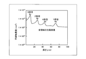
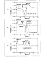
- FIG. 8 is a characteristic diagram showing the relationship between the average range of conventional proton irradiation and the carrier concentration.
- FIG. 8 shows the carrier concentration of the silicon substrate measured by the SR method after the silicon substrate was irradiated with protons and heat-treated at 350 ° C.
- Fig. 8 (a) sets the average range of proton irradiation to 50 ⁇ m
- Fig. 8 (b) sets the average range of proton irradiation to 20 ⁇ m
- Fig. 8 (c) shows the average range of proton irradiation. It is a case where it is 10 micrometers. Each horizontal axis is the distance (depth) from the proton incident surface. In the mean range of 10 ⁇ m of proton irradiation in FIG.
- An object of the present invention is to provide a semiconductor device provided with a region having a low degree of disorder and a high concentration of hydrogen related donors and a method of manufacturing the semiconductor device in order to solve the problems of the prior art described above. .
- a method of manufacturing a semiconductor device comprises: a breakdown voltage holding pn junction provided on one main surface side of an n-type semiconductor substrate; An n-type field stop layer provided inside the other main surface side of the n-type semiconductor substrate and having a resistance lower than that of the n-type semiconductor substrate for suppressing the spread of a depletion layer from the pn junction for breakdown voltage holding; A method of manufacturing a semiconductor device having the following features.
- the proton irradiation process of forming the n-type field stop layer inside the other main surface side of the n-type semiconductor substrate by repeatedly performing proton irradiation a plurality of times from the other main surface of the n-type semiconductor substrate is performed.
- the proton irradiation step every time the proton irradiation is repeated, the next proton irradiation is performed so as to compensate for the decrease in mobility due to the disorder remaining in the previous proton irradiation.
- the irradiation depth of the next proton irradiation is preferably shallower than the irradiation depth of the previous proton irradiation.
- the proton irradiation is repeated on the basis of.
- the proton irradiation step is formed by the first proton irradiation based on the peak of the impurity concentration distribution formed by the second and subsequent proton irradiations. It is also preferable to adjust the acceleration energy and the dose of the proton irradiation so as to compensate the portion where the impurity concentration is lowered by the disorder.
- the depth at which the mobility is most reduced due to disorder after the previous proton irradiation is the next proton irradiation. It is preferable to set it as the irradiation depth of.
- the common logarithm value log (E) of the acceleration energy E of the proton irradiation is y
- the semiconductor device according to the present invention can be a diode or an IGBT.
- the semiconductor device has the following features.
- a breakdown voltage holding pn junction is provided on one main surface side of the n-type semiconductor substrate.
- An n-type field stop layer having a resistance lower than that of the n-type semiconductor substrate is provided inside the other main surface side of the n-type semiconductor substrate to suppress the spread of the depletion layer from the breakdown voltage holding pn junction. ing.
- the n-type field stop layer has an impurity concentration distribution having a plurality of impurity concentration peaks at different positions in the depth direction of the n-type semiconductor substrate.
- the impurity concentration peak closest to one main surface of the n-type semiconductor substrate is located at a depth of 15 ⁇ m or more from the other main surface of the n-type semiconductor substrate.
- the distance between the position of the impurity concentration peak of the n-type field stop layer and the other main surface of the n-type semiconductor substrate is the impurity adjacent to one main surface side of the n-type semiconductor substrate of the impurity concentration peak. It is half or more of the distance between the position of the concentration peak and the other main surface of the n-type semiconductor substrate.
- the impurity concentration peak on the other main surface side of the n-type semiconductor substrate among the plurality of impurity concentration peaks is the other of the n-type semiconductor substrate It is preferable to be located in the depth of 6 micrometers or more and 15 micrometers or less from the main surface of these.
- the semiconductor device and the method for manufacturing the semiconductor device according to the present invention it is possible to reduce the degree of disorder appearing in the semiconductor substrate after the proton irradiation and the heat treatment. Further, according to the semiconductor device and the method of manufacturing the semiconductor device according to the present invention, it is possible to suppress the occurrence of characteristic defects such as an increase in leakage current and to form a region having a high hydrogen related donor concentration. .
- FIG. 1 is a characteristic diagram showing the impurity concentration profile of the n-type FS layer of the semiconductor device according to the first embodiment.
- FIG. 2 is a cross-sectional view schematically showing the structure of a general IGBT.
- FIG. 3 is a flowchart showing an outline of a method of manufacturing a semiconductor device according to the first embodiment.
- FIG. 4 is a characteristic diagram showing another example of the impurity concentration profile of the n-type FS layer of the semiconductor device according to the first embodiment.
- FIG. 5 is a characteristic diagram showing the impurity concentration profile of the n-type FS layer of the semiconductor device according to the second embodiment.
- FIG. 6 is a characteristic diagram showing the impurity concentration profile of the n-type FS layer of the semiconductor device according to the third embodiment.
- FIG. 7 is a characteristic diagram showing another example of the impurity concentration profile of the n-type FS layer of the semiconductor device according to the third embodiment.
- FIG. 8 is a characteristic diagram showing the relationship between the average range of conventional proton irradiation and the carrier concentration.
- FIG. 9 is a characteristic diagram showing the threshold voltage at which the voltage waveform starts to vibrate.
- FIG. 10 is an explanatory view showing the structure and net doping concentration of a general IGBT.
- FIG. 11 shows an oscillation waveform at turn-off of the IGBT.
- FIG. 12 is a characteristic diagram showing the relationship between the range of protons and the acceleration energy of protons in the semiconductor device according to the present invention.
- FIG. 13 is a chart showing the position condition of the FS layer which the depletion layer first reaches in the semiconductor device according to the present invention.
- n and p in the layer or region having n or p, it is meant that electrons or holes are majority carriers, respectively.
- + and-attached to n and p mean that the impurity concentration is relatively higher or lower than the layer or region to which it is not attached, respectively.
- the same components are denoted by the same reference numerals and redundant description will be omitted.
- the present invention is not limited to the description of the embodiments described below, as long as the scope of the present invention is not exceeded.
- FIG. 2 is a cross-sectional view schematically showing the structure of a general IGBT.
- FIG. 2A shows a schematic cross-sectional view of an IGBT having an n-type FS (field stop) layer 3 formed by a general conventional proton irradiation method.
- FIG. 2B shows the impurity concentration profile of the n-type FS layer 3 measured by the well-known spread resistance measurement (SR) method.
- SR spread resistance measurement
- FIG. 2A is also used as a cross-sectional view in the description of the semiconductor device according to the present invention.
- the difference between the IGBT manufactured by the method of manufacturing a semiconductor device according to the present invention and the IGBT manufactured by the conventional method is the impurity concentration profile of the n-type FS layer 3 shown in FIG. 2B.
- the impurity concentration profile of the n-type FS layer 3 of the IGBT according to the present invention will be described later.
- FIG. 10 is an explanatory view showing the structure and net doping concentration of a general IGBT.
- the p base layer 33, the n + emitter layer 2, and the gate insulating film 43 are provided on one principal surface side of the n ⁇ drift layer 1 (high resistance semiconductor layer) made of an n type semiconductor substrate.
- a gate electrode 42 is formed.
- components other than the n + emitter layer 2 of the MOS gate structure are omitted for simplification.
- the n-type FS layer 3 includes a first stage 6a, a second stage 6b, and a third stage 6c of a plurality of impurity concentration peaks (proton peaks) at different positions in the substrate depth direction.
- the distance from the emitter electrode 31 of each proton peak is, for example, 60, 90, 115 ⁇ m in order.
- An emitter electrode 31 in contact with the p base layer 33 and the n + emitter layer 2 is formed on the front surface side of the substrate.
- a collector electrode 32 in contact with the p collector layer 4 is formed on the back surface of the substrate.
- the n-type leak stop layer 38 is formed in contact with the p collector layer 4, it may be omitted.
- n-type FS layer 3 by proton irradiation is a well-known technique.
- a layer hereinafter referred to as a hydrogen related donor layer
- crystal defects generated along with proton irradiation Needs to be left unrecovered by annealing treatment after proton irradiation.
- the impurity concentration peak (hereinafter referred to as a proton peak) 6 a of the n-type FS layer 3 becomes large, but disorder 7 also remains. Problems such as an increase in leakage current may occur due to disorder 7.
- the feature of the present invention relates to the improvement of the proton irradiation method for suppressing the occurrence of disorder 7 generated in the n-type FS layer 3 when the n-type FS layer 3 is formed by proton irradiation.
- the other parts (the MOS gate structure on the front surface of the substrate, the oxide film, the pn junction, the electrode, the protective film, etc.) of the IGBT 10 can be formed by the same manufacturing method as known manufacturing methods. Therefore, in the following description, detailed description of the part of the known IGBT manufacturing method is omitted.
- FIG. 3 is a flowchart showing an outline of a method of manufacturing a semiconductor device according to the first embodiment.
- a p base layer (not shown), an n + emitter layer 2, a gate insulating film (not shown), a gate electrode (not shown), etc. on the front surface of an n type semiconductor substrate (wafer)
- a front surface forming step is performed to form a MOS gate structure or the like (FIG. 3A).
- a front Al electrode process is performed to form an emitter electrode (not shown) made of, for example, an aluminum (Al) electrode in common conductive contact with both surfaces of the p base layer and the n + emitter layer 2 (see FIG. 3 (b).
- a surface protection film forming step is performed to form a polyimide film to be a surface protection film on the front surface side of the n-type semiconductor substrate (FIG. 3C).
- a thinning process is performed to grind the back surface of the n-type semiconductor substrate (FIG. 3D).
- the n-type FS layer 3 has an impurity concentration profile having a plurality of impurity concentration peaks (proton peaks) at different positions in the substrate depth direction by a plurality of times of proton irradiation in the back surface diffusion layer process described above.
- the multiple proton irradiation methods in the back surface diffusion layer process will be described later.
- FIG. 1 is a characteristic diagram showing the impurity concentration profile of the n-type FS layer of the semiconductor device according to the first embodiment.
- FIG. 1 shows the impurity concentration profile of the n-type FS layer 3 after proton irradiation from the back surface of the n-type semiconductor substrate and annealing treatment in manufacturing the semiconductor device shown in FIG.
- the vertical axis is the impurity concentration of the n-type FS layer 3
- the horizontal axis is the depth from the back surface of the n-type semiconductor substrate.
- the value of mobility of a silicon crystal is generally used as the value of mobility used when converting the resistivity and carrier concentration from the spreading resistance in a measuring device or the like. Therefore, the converted carrier concentration is calculated to be lower than the concentration of the activated dopant, reflecting the decrease in actual mobility.
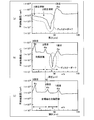
- FIG. 1 shows the transition of the impurity concentration profile of the n-type FS layer 3 when the proton irradiation and the annealing treatment are repeated until the disorder disappears or the disorder degree becomes smaller (also in FIGS. 5 to 7).
- FIG. 1A shows the impurity concentration profile of the n-type FS layer 3 after the first proton irradiation and annealing treatment. As shown in FIG. 1A, one peak (proton peak, first step 6a) having a high impurity concentration is formed deep from the back surface of the n-type FS layer 3 after the first proton irradiation and annealing treatment.
- FIG. 1A shows that when there is disorder 7, the decrease in mobility is reflected in the impurity concentration converted from the spreading resistance, and the impurity concentration appears as a decrease.
- FIG. 1 (b) shows the impurity concentration profile of the n-type FS layer 3 after the second and third proton irradiations and the annealing treatment.
- FIG. 1 (b) shows the impurity of the n-type FS layer 3 when the proton peak of the second step 6b is formed at a position shallower from the back surface of the substrate than the intermediate position between the back surface of the substrate and the proton peak position of the first step 6a. It is a concentration profile.
- a proton peak of the third step 6c is also formed at a position closer to the back surface of the substrate. As shown in FIG.
- the impurity of the silicon substrate is in the region between the proton peak of the first stage 6a and the proton peak of the second stage 6b.
- disorder 7 in which the impurity concentration is much lower than the concentration.
- the depletion layer extending from the breakdown voltage main junction of the IGBT 10 is disorder 7 when turned off. When it penetrates into the region, the disorder 7 becomes the generation center of the leakage current, which is not preferable because the leakage current increases.
- FIG. 1C shows the impurity concentration profile of the n-type FS layer 3 when the proton irradiation and annealing treatment for the third time are performed after performing the second proton irradiation and annealing treatment while adjusting the irradiation position. .
- the irradiation conditions such as the acceleration energy of protons are changed from the substrate back surface side, and the first step 6a A plurality of times of proton irradiation are sequentially performed at a position shallower than the proton peak position of the substrate from the back surface of the substrate to perform an annealing process. That is, after the first proton irradiation shown in FIG. 1A, a hydrogen related donor layer is formed in the n-type FS layer 3 by plural times of proton irradiation, and the hydrogen related donor concentration of the n-type FS layer 3 is compensated. .
- the degree of disorder 7 formed in the first proton irradiation (the degree of decrease in impurity concentration due to disorder 7) can be reduced, or disorder 7 can be eliminated. it can.
- the reason why the degree of disorder 7 decreases is presumed to be that the injected protons (i.e., hydrogen atoms) terminate dangling bonds present in the portion where the degree of disorder 7 is the largest.
- the distribution of disorder 7 formed by the first proton irradiation is measured by the SR method. Then, with respect to the impurity concentration profile of the n-type FS layer 3 of FIG. 1A, to reduce the degree of disorder 7 or eliminate disorder 7 based on the depth of disorder 7 from the back surface of the substrate. 1 and 2.
- the second and third proton irradiations are performed at positions shallower than the proton peak position of the first step 6a in FIG. 1A from the back surface of the substrate, for example, the second and third irradiation positions shown by arrows in FIG. Do.
- the first to third proton irradiations are performed at different acceleration energies.
- the proton peak of the second step 6b is formed at a position shallower from the back surface of the substrate than the intermediate position between the back surface of the substrate and the proton peak of the first step 6a, the proton peak of the first step 6a and Disorder 7 remains at a position intermediate to the proton peak of the eye 6 b (FIG. 1 (b)).
- the reason is that the proton irradiation position of the second stage 6b is not appropriate.
- the distance b between the proton peak position of the first stage 6a and the proton peak position of the second stage 6b is from the distance a between the proton peak position of the second stage 6b and the irradiation surface (substrate rear surface) This is because the compensation effect of doping by the proton peak (hydrogen related donor layer) of the second stage 6b is reduced.
- the disorder 7 can be substantially eliminated by setting the second proton irradiation position to the disorder 7 position or its vicinity caused by the first proton irradiation. .
- the second proton irradiation position is adjusted to increase the doping compensation effect by the proton peak (hydrogen related donor layer) of the second stage 6b.
- the distance between the second proton irradiation position and the back surface of the substrate may be, for example, half or more of the distance between the first proton irradiation position and the back surface of the substrate.
- the average range of the second proton irradiation should be at least half the average range of the first proton irradiation.
- the average range is the depth from the back surface of the substrate of the peak concentration position of the impurity concentration distribution of the n-type FS layer 3 represented by the Gaussian distribution. Specifically, the average range is the depth from the back surface of the substrate to the proton peak position.
- the method of setting the second proton irradiation position will be described later.
- the difference between the second proton irradiation position shown in FIG. 1 (c) and the second proton irradiation position shown in FIG. 1 (b) is indicated by a white arrow in FIG. 1 (c).
- an example of specific ion implantation conditions of three times of proton irradiation in the case where the impurity concentration profile of the n-type FS layer 3 without disorder 7 is obtained in this way is shown below.
- the acceleration energy and dose of proton irradiation (ie, first proton irradiation) to form a first stage 6a proton peak are 2.3 MeV and 3 ⁇ 10 13 / cm 2 , respectively.
- the acceleration energy and dose of proton irradiation (ie, second proton irradiation) to form a second stage 6b proton peak are 1.5 MeV and 3 ⁇ 10 13 / cm 2 , respectively.
- the acceleration energy and dose of proton irradiation (ie, third proton irradiation) to form a third stage 6c proton peak are 0.5 MeV and 2 ⁇ 10 14 / cm 2 , respectively.
- the average range of the third proton irradiation is, for example, about 6 ⁇ m to 15 ⁇ m from the back surface of the substrate.
- the annealing treatment after proton irradiation is preferably performed at a temperature of about 450 ° C. for about 5 hours in a reducing atmosphere (for example, a hydrogen atmosphere with a hydrogen concentration of 3% or a nitrogen atmosphere containing hydrogen).
- specific ion implantation conditions of four times of proton irradiation are as follows.
- the acceleration energy and dose of the first proton irradiation are 1.5 MeV and 2 ⁇ 10 13 / cm 2 , respectively.
- the acceleration energy and dose of the second proton irradiation are 1.1 MeV and 2 ⁇ 10 13 / cm 2 , respectively.
- the acceleration energy and dose of the third proton irradiation are 0.8 MeV and 5 ⁇ 10 13 / cm 2 , respectively.
- the acceleration energy and dose of proton irradiation (ie, fourth proton irradiation) to form the fourth proton peak are 0.4 MeV and 1 ⁇ 10 14 / cm 2 , respectively.
- the annealing treatment after proton irradiation is preferably performed at a temperature of about 380 ° C. to 450 ° C. for about 5 hours in a reducing atmosphere.
- the positional relationship between the proton peak of the first stage 6a and the proton peak of the second stage 6b is an important point of the present invention.
- disorder 7 is formed on the irradiation surface (substrate rear surface) side of the proton peak position of the first step 6a.
- the position where the degree of disorder 7 is the largest is where the decrease in mobility is the largest and where the impurity concentration measured by the SR method is the lowest. That is, the degree of disorder 7 is largest at a position deeper than the intermediate position between the back surface of the substrate and the proton peak position of the first stage 6a on the proton peak side of the first stage 6a.
- the region where the silicon lattice receives the most energy from the protons irradiated to the silicon substrate is the position where the mobility is lowest in the region where disorder 7 occurs, that is, the position where the carrier concentration is lowest.
- the position where the proton peak of the second step 6b is formed by the second proton irradiation may be at or near the position where the degree of disorder 7 is the largest by the first proton irradiation.
- the position at which the proton peak of the second step 6b is formed by the second proton irradiation is the proton of the first step 6a from the back of the substrate than the intermediate position between the substrate back and the proton peak position of the first step 6a. It is a deep position on the peak position side.
- the difference between the range Rp of the first proton irradiation and the range Rp of the second proton irradiation be smaller than the range Rp of the second proton irradiation. If the difference between the range Rp of the first proton irradiation and the range Rp of the second proton irradiation is equal to or less than half the range Rp of the second proton irradiation, the disorder 7 is reliably removed. , More preferred.
- the distance b between the proton peak position of the first stage 6a (the peak position of the carrier concentration measured by SR method) and the proton peak position of the second stage 6b is the proton peak position of the second stage 6b and the back surface of the substrate Is preferably smaller than the distance a, and more preferably half or less.
- the difference between the proton irradiation range Rp and the second proton irradiation range Rp is preferably smaller, and more preferably half or less.
- the distance b between the position where the carrier concentration measured by the SR method is the lowest and the proton peak position of the second step 6b is smaller than the distance a between the proton peak position of the second step 6b and the substrate back surface Is preferable, and more preferably half or less.
- the total number of proton peaks formed inside the n-type FS layer 3 is preferably 3 or more.
- the shallowest position that is, the proton peak closest to the back surface of the substrate
- the depletion layer does not reach p collector layer 4 (so that the desired field stop function is obtained). It is formed to a depth of less than about 5 ⁇ m. Therefore, when the total number of proton peaks formed inside n-type FS layer 3 is two, the second stage proton peak formed at the shallowest position is 5 ⁇ m from the back surface of the substrate to obtain the desired field stop function.
- the first stage proton peak formed at the deepest position is, for example, about 50 ⁇ m from the back surface of the substrate.
- the proton peak at the first stage and the proton peak at the second stage are separated by 45 ⁇ m, disorder easily occurs. Therefore, it is preferable to form another proton peak between the proton peak formed at a position shallow from the back surface of the substrate and the proton peak formed at a position deep from the back surface of the substrate.
- the hydrogen-related donor concentration of the n-type FS layer 3 is compensated as described above, so that the decrease in mobility can be reduced and disorder can be removed.
- FIG. 4 is a characteristic diagram showing another example of the impurity concentration profile of the n-type FS layer of the semiconductor device according to the first embodiment.
- the fourth proton irradiation is performed on disorder 7 remaining between the proton peak position of the first stage 6a and the proton peak position of the second stage 6b.
- protons of the first to third stages 6a to 6c are formed by the first to third proton irradiation.
- disorder 7 remains between the proton peak position of the first stage 6a and the proton peak position of the second stage 6b, as shown in FIG. 1 (b).
- the fourth order of proton irradiation is performed on disorder 7 remaining between the proton peak position of the first stage 6a and the proton peak position of the second stage 6b.
- a proton peak of the fourth stage 6 d is formed between the proton peak position of the first stage 6 a and the proton peak position of the second stage 6 b.
- the order 7 can be eliminated or the degree of disorder 7 can be reduced.
- specific ion implantation conditions of four times of proton irradiation in the case where the impurity concentration profile of the n-type FS layer 3 without disorder 7 is obtained in this way is shown below.
- the acceleration energy and dose of the first proton irradiation are 1.5 MeV and 1 ⁇ 10 13 / cm 2 , respectively.
- the acceleration energy and dose of the second proton irradiation are 1.1 MeV and 1 ⁇ 10 13 / cm 2 , respectively.
- the acceleration energy and dose of the third proton irradiation are 0.8 MeV and 2 ⁇ 10 13 / cm 2 , respectively.
- the acceleration energy and dose of proton irradiation (ie, fourth proton irradiation) to form a fourth stage 6d proton peak are 0.4 MeV and 3 ⁇ 10 14 / cm 2 , respectively.
- the average range of the fourth proton irradiation is, for example, about 6 ⁇ m to 15 ⁇ m from the back surface of the substrate.
- the annealing treatment after proton irradiation is preferably performed at a temperature of about 380 ° C. for about 5 hours in a reducing atmosphere (for example, a hydrogen atmosphere with a hydrogen concentration of 3% or a nitrogen atmosphere containing hydrogen).
- the range of proton irradiation is set to the above condition to perform proton irradiation a plurality of times, or the distance between proton peaks formed by each proton irradiation is By performing proton irradiation a plurality of times so as to satisfy the above conditions, the disorder which has largely occurred in the silicon substrate by proton irradiation in the conventional method is eliminated, or the degree of disorder is such that the element characteristics are not adversely affected. It can be made smaller.
- n-type FS layer having no disorder or a small degree of disorder, and a desired field stop function having no part where the impurity concentration (carrier concentration) is greatly reduced or little decrease in impurity concentration.
- An n-type FS layer can be formed. As a result, it is possible to manufacture a semiconductor device having an FS structure in which characteristic deterioration such as leakage current is suppressed.
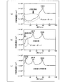
- FIG. 5 is a characteristic diagram showing the impurity concentration profile of the n-type FS layer of the semiconductor device according to the second embodiment.
- the method of manufacturing a semiconductor device according to the second embodiment differs from the method of manufacturing a semiconductor device according to the first embodiment in that a plurality of proton irradiations for eliminating disorder 17 or reducing the degree of disorder 17 are performed. This is a point performed sequentially from the deep position side to the shallow position side from the rear surface side of the substrate in the region of disorder 17.
- the configuration of the semiconductor device manufactured by the method of manufacturing a semiconductor device according to the second embodiment is, for example, an IGBT shown in FIG. 2A as in the first embodiment.
- the manufacturing method other than the proton irradiation method for forming the n-type FS layer 3 of the semiconductor device according to the second embodiment is the same as the manufacturing method of the semiconductor device according to the first embodiment. Therefore, only the proton irradiation method for forming the n-type FS layer 3 will be described (the same applies to the third embodiment).
- 5 (a) to 5 (c) show impurity concentration profiles of the n-type FS layer 3 after the first to third proton irradiations and annealing.
- FIG. 5A by forming a proton peak of the first step 16a at a predetermined depth from the back surface of the substrate by the first proton irradiation, as in the first embodiment, the back surface of the substrate is one step.
- a region of disorder 17 (a portion surrounded by a dotted line) is formed between the proton peak position of the eye 16a.
- the distribution of disorder 17 formed by the first proton irradiation is measured by the SR method.
- the second proton irradiation is performed at a position deep from the back surface of the substrate in the region of the disorder 17 formed by the first proton irradiation (for example, a second irradiation position indicated by an arrow in FIG. 5A).
- the proton peak of the second step 16b is formed at a position deep from the back surface of the substrate in the region of disorder 17, and the disorder 17 at the position deep from the back surface of the substrate is eliminated.
- the degree of disorder 17 can be reduced.
- the region of disorder 17 remaining between the back surface of the substrate and the proton peak position of the second step 16b (eg A third proton irradiation is performed on the third irradiation position (indicated by an arrow in FIG. 5B).
- the proton peak of the third step 16c is formed at a shallow position from the back surface of the substrate, and the disorder 17 of the entire n-type FS layer 3 is eliminated or the degree of disorder 17 is reduced. can do.
- the proton irradiation method according to the second embodiment described above exemplifies the case where the disorder 17 in the entire n-type FS layer 3 disappears or the degree of disorder 17 decreases by the third proton irradiation.
- the area of disorder 17 remains between the proton peak position of stage 16c, the position of deep in the area of disorder 17 remaining between the back surface of the substrate and the proton peak position of stage 16c.
- the fourth proton irradiation may be performed.
- the acceleration energy and dose of the first proton irradiation are 2.0 MeV (average range 47.7 ⁇ m) and 3 ⁇ 10 13 / cm 2 , respectively.
- the acceleration energy and dose of the second proton irradiation are 1.5 MeV (average range 30.3 ⁇ m) and 3 ⁇ 10 13 / cm 2 , respectively.
- the acceleration energy and dose of the third proton irradiation are 0.5 MeV (average range 6.0 ⁇ m) and 2 ⁇ 10 14 / cm 2 , respectively.
- the annealing treatment after proton irradiation is preferably performed at a temperature of about 380 ° C.
- Annealing conditions after proton irradiation may be, for example, about 1 to 10 hours at a temperature of about 300 ° C. to 450 ° C., depending on the specification of the n-type FS layer 3 required.
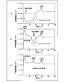
- FIG. 6 is a characteristic diagram showing the impurity concentration profile of the n-type FS layer of the semiconductor device according to the third embodiment.
- the semiconductor device manufacturing method according to the third embodiment is different from the semiconductor device manufacturing method according to the first embodiment in that multiple proton irradiations for eliminating disorder 27 or reducing the degree of disorder 27 are performed. This is a point performed sequentially from the shallow position side to the deep position side from the rear surface side of the substrate in the region 27 of disorder.
- 6 (a) to 6 (c) show impurity concentration profiles of the n-type FS layer 3 after the first to third proton irradiation and annealing.
- FIG. 6A by forming a proton peak of the first step 26a at a predetermined depth from the back surface of the substrate by the first proton irradiation, as in the first embodiment, the back surface of the substrate is one step.
- a region of the disorder 27 is formed between the proton peak position of the eye 26a.
- the second proton irradiation is performed at a position shallower from the back surface of the substrate in the region of the disorder 27 formed by the first proton irradiation (for example, a second irradiation position indicated by an arrow in FIG. 6A).
- a second irradiation position indicated by an arrow in FIG. 6A the proton peak of the second step 26b is formed at a position shallower from the back surface of the substrate in the region of disorder 27.
- the disorder 27 at this position is eliminated or disordered 27 Can be reduced.
- FIG. 7 is a characteristic diagram showing another example of the impurity concentration profile of the n-type FS layer of the semiconductor device according to the third embodiment.
- FIGS. 7 (a) and 7 (b) after the proton peaks of the second and third steps 26b and 26c are formed by the second and third proton irradiations, the proton peak position of the first step 26a and the third step
- a region of disorder 27 remains between the proton peak position of 26 c and the remaining 27 (for example, the fourth stage irradiation position indicated by the arrow in FIG. 7B)
- the fourth proton irradiation is performed You may
- a proton peak of the fourth step 26d is formed between the proton peak position of the first step 26a and the proton peak position of the third step 26c, and n
- the degree of disorder 27 can be eliminated or the degree of disorder 27 can be reduced as a whole.
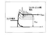
- FIG. 11 shows an oscillation waveform at turn-off of the IGBT. If the collector current is 1/10 or less of the rated current, oscillation may occur before the turn-off ends because the accumulated carriers are small. With the collector current fixed at a certain value, the IGBT is turned off at different power supply voltages V CC . At this time, when V CC exceeds a predetermined value, an additional overshoot occurs after the peak value of the normal overshoot voltage is exceeded in the collector-emitter voltage waveform. Then, this additional overshoot (voltage) triggers the subsequent waveform to vibrate.
- the threshold voltage at which the voltage waveform starts to oscillate is called the oscillation start threshold V RRO .
- the higher V.sub.RRO is preferable because it indicates that the IGBT does not oscillate at turn-off.
- Oscillation start threshold V RRO is, p-type base layer of the IGBT and the n - n from the pn junction between the drift layer - depletion layer extending the drift layer (strictly, because the holes are present space charge region), a plurality of It depends on the position of the first stage proton peak that reaches first among the proton peaks. The reason is as follows. When the depletion layer extends from the p-type base layer on the surface to the n - drift layer at turn-off, the end of the depletion layer reaches the first n-type FS layer, the expansion is suppressed and the discharge of accumulated carriers is weakened. As a result, carrier exhaustion is suppressed and oscillation is suppressed.
- the depletion layer extends along the depth direction from the pn junction between the p base layer and the n ⁇ drift layer toward the collector electrode. Therefore, the peak position of the n-type FS layer at which the depletion layer edge first reaches is the n-type FS layer closest to the pn junction. Therefore, n - -type thickness of the semiconductor substrate (thickness of a portion held with the emitter and collector electrodes) W0, the peak position of the n-type FS layer depletion end first reaches the collector electrode and the n - Let X be the depth from the interface with the back surface of the semiconductor substrate (hereinafter referred to as the distance from the back surface).
- the distance index L is introduced.
- the distance index L is expressed by the following equation (1).
- the distance index L shown in the above equation (1) is a depletion layer (space charge region) extending from the pn junction to the n ⁇ drift layer 21 when the collector-emitter voltage V CE becomes the power supply voltage V CC at turn-off. It is an index indicating the distance from the pn junction of the end (depletion layer end). In the interior fraction of the square root, the denominator indicates the space charge density of the space charge region (simply, depletion layer) at turn-off.
- the space charge density ⁇ is described by the concentration of holes p running through the space charge region (depletion layer) at turn-off and the average donor concentration N dm of the n ⁇ drift layer, and the electron concentration is negligible. Since there is no acceptor, it can be expressed as ⁇ q q (p + Ndm).
- the FS layer has a function of making it difficult for the n-type FS layer to spread the expansion of the space charge region spreading at turn-off by making the doping concentration higher than that of the n ⁇ drift layer. If the peak position of the FS layer at which the depletion layer first reaches when the collector current of the IGBT starts to decrease from the cutoff current due to the turning off of the MOS gate is in this space charge region, accumulated carriers remain in the n - drift layer In this state, since the expansion of the space charge region can be suppressed, the sweeping out of the remaining carriers can be suppressed.
- FIG. 13 is a chart showing the position condition of the FS layer which the depletion layer first reaches in the semiconductor device according to the present invention.
- the element As shown in FIG. 13, at each rated voltage, safety design is performed such that the element (IGBT) has a withstand voltage about 10% higher than the rated voltage. Then, as shown in FIG. 13, the total thickness of the n - type semiconductor substrate (thickness at the time of finishing after thinning by grinding or the like) and the average of the n - drift layer so that the on voltage and the turn off loss become sufficiently low. Specific resistivity. The average is the average concentration and resistivity of the entire n - drift layer including the FS layer. Depending on the rated voltage, the rated current density also becomes a typical value as shown in FIG.
- the rated current density is set such that the energy density determined by the product of the rated voltage and the rated current density is approximately a constant value, and is approximately the value shown in FIG.
- the distance index L becomes the value described in FIG.
- the distance X from the back surface of the peak position of the n-type FS layer to which the depletion layer edge first reaches is the thickness of the n ⁇ -type semiconductor substrate with a value where ⁇ is 0.7 to 1.6 for this distance index L It is the value subtracted from W0.
- FIG. 9 is a characteristic diagram showing the threshold voltage at which the voltage waveform starts to vibrate.
- FIG. 9 shows the dependence of V RRO on this ⁇ for several typical rated voltages (600 V, 1200 V, 3300 V).
- the vertical axis is a value obtained by standardizing V RRO with the rated voltage V rate . It can be seen that for all three rated voltages, V RRO can be rapidly increased when ⁇ is less than or equal to 1.4. When ⁇ is in the range of 0.8 to 1.3, any of the rated voltages is a region where V RRO can be sufficiently high. More preferably, V RRO can be maximized if ⁇ is in the range of 0.9 to 1.2.
- the distance X from the back surface of the peak position of the n-type FS layer to which the depletion layer edge first reaches is preferably such that the coefficient ⁇ of the distance index L is in the above range.
- acceleration energy of proton is It may be determined from the characteristic graph of FIG. 12 shown below.
- the inventors of the present invention have intensively studied the proton range Rp (peak position of the n-type FS layer) and the proton acceleration energy E, the logarithm log (Rp) of the proton range Rp to x, the proton acceleration energy Assuming that the log log (E) of E is y, it has been found that there is a relationship of the following equation (2).
- FIG. 12 is a characteristic diagram showing the relationship between the range of protons and the acceleration energy of protons in the semiconductor device according to the present invention.
- FIG. 12 shows the acceleration energy of protons to obtain the desired range of protons.
- the horizontal axis in FIG. 12 is the logarithm log (Rp) of the proton range Rp, and indicates the corresponding range Rp ( ⁇ m) in parentheses below the axial value of log (Rp).
- the vertical axis is the logarithm log (E) of the acceleration energy E of proton, and the acceleration energy E of the corresponding proton is shown in the parentheses on the left side of the axis value of log (E).
- the acceleration energy E of proton irradiation is calculated and set from the average range Rp of desired protons using the above-mentioned fitting equation, and the actual acceleration energy E 'and the actual spreading resistance when protons are injected into silicon
- the relationship with the average range Rp ′ (proton peak position) obtained by the (SR) measurement method or the like may be considered as follows. If the actual acceleration energy E ′ is in the range of about E ⁇ 5% with respect to the calculated value E of the acceleration energy, the actual range Rp ′ is also in the range of about ⁇ 5% of the desired Rp, It will be within the range of measurement error. Therefore, the variation of the actual average range Rp 'from Rp on the electrical characteristics of the IGBT is sufficiently small to be negligible.
- the acceleration energy E of protons necessary to obtain the desired proton range Rp can be determined.
- the acceleration energy E of each of the protons for forming the FS layer described above also uses the above equation (2), and the spread resistance measurement method (SR method) of a sample actually irradiated with protons by the above acceleration energy is known. It agrees well with the measured value measured by. Therefore, by using the above equation (2), it is possible to predict the acceleration energy E of the necessary proton based on the proton range Rp with extremely high accuracy.
- the present invention has been described by way of an IGBT in the present invention, the present invention is not limited to this and can be applied to a diode or the like. Furthermore, the present invention is applicable to semiconductor devices with withstand voltages of 600 V, 1200 V, 1700 V, 3300 V, 4500 V and 6000 V, for example.
- the semiconductor device and the method for manufacturing the semiconductor device according to the present invention are useful for a power semiconductor device used for a power conversion device such as a converter or an inverter.
Landscapes
- Engineering & Computer Science (AREA)
- Microelectronics & Electronic Packaging (AREA)
- Power Engineering (AREA)
- Physics & Mathematics (AREA)
- Condensed Matter Physics & Semiconductors (AREA)
- General Physics & Mathematics (AREA)
- Computer Hardware Design (AREA)
- Ceramic Engineering (AREA)
- Manufacturing & Machinery (AREA)
- High Energy & Nuclear Physics (AREA)
- Health & Medical Sciences (AREA)
- Toxicology (AREA)
- Thin Film Transistor (AREA)
- Metal-Oxide And Bipolar Metal-Oxide Semiconductor Integrated Circuits (AREA)
- Insulated Gate Type Field-Effect Transistor (AREA)
- Electrodes Of Semiconductors (AREA)
Abstract
Multiple proton irradiations are repeatedly performed from the reverse surface of an n-type semiconductor substrate, which functions as an n- drift layer, and an n-type FS layer having a resistance that is lower than that of the n-type semiconductor substrate is formed in the interior of the n- drift layer on the side nearer the reverse surface of the substrate. During the multiple proton irradiations performed in order to form the n-type FS layer, each subsequent proton irradiation is performed so as to compensate for a decrease in mobility due to a disorder (7) left from the previous proton irradiation. Each of the second and subsequent proton irradiations is performed so as to target the position of the disorder (7) formed by the preceding proton irradiation. It is thereby possible to form an n-type FS layer that has little disorder (7), that makes it possible to minimize the occurrence of characteristic defects such as an increase in leak current, and that has a high-concentration hydrogen-related donor layer, even after proton irradiation and heat treatment.
Description
本発明は、半導体装置および半導体装置の製造方法に関する。
The present invention relates to a semiconductor device and a method of manufacturing the semiconductor device.
回転モーターやサーボモーターの制御に不可欠なコンバーター-インバーター等の電力変換装置が公知である。このような電力変換装置の高効率化、省電力化のために、それらに搭載されるパワーダイオードや絶縁ゲートバイポーラトランジスタ(IGBT)等の半導体装置の低損失化が強く求められる。
A power converter such as a converter-inverter, which is essential for controlling a rotary motor or a servomotor, is known. In order to increase the efficiency and save power of such power conversion devices, it is strongly required to reduce the loss of semiconductor devices such as power diodes and insulated gate bipolar transistors (IGBTs) mounted thereon.
このような低損失化の要求に対する改善策の一つとして、ダイオードやIGBTについては、素子構造を構成する半導体層のうち最も高抵抗で厚い層であるドリフト層を薄くすることで、オン電流による電圧降下を少なくしてオン損失を小さくするフィールドストップ(FS)層構造が知られている。このFS層構造は、ドリフト層の耐圧主接合から遠い側のドリフト層内部に、ドリフト層より高不純物濃度でかつドリフト層と同導電型のFS層を設けた構造である。このFS層を設けることにより、オフ時に耐圧主接合から高抵抗のドリフト層中に伸びる空乏層が抑えられるため、ドリフト層を薄くしてもパンチスルーを防ぐことができる。
As one of the remedies for such a demand for low loss, the diode or IGBT is reduced in on current by thinning the drift layer which is the highest resistance thick layer among the semiconductor layers constituting the element structure. A field stop (FS) layer structure is known which reduces voltage drop and reduces on-loss. This FS layer structure is a structure in which an FS layer having a higher impurity concentration than the drift layer and the same conductivity type as the drift layer is provided inside the drift layer on the side far from the withstand voltage main junction of the drift layer. By providing this FS layer, a depletion layer extending from the breakdown voltage main junction into the high resistance drift layer can be suppressed at the time of off, so punch-through can be prevented even if the drift layer is thinned.
一方、パワーデバイスの作製(製造)では、FZ(フローティングゾーン)法によるインゴットから切り出されたウエハ(以下、FZウエハとする)がコストダウンのために用いられる。FZウエハは、製造プロセスへの投入時はウエハ割れを少なくするために厚さ600μm以上の厚い状態で投入されるが、最終的にはオン損失低減のために製造プロセス中に薄化され設計耐圧に必要な厚さにまで薄く研磨される。特に、IGBTなどのMOS(金属-酸化膜-半導体)型デバイスでは、FZウエハを薄くするための研磨を、FZウエハのおもて面側にMOSゲート構造、周縁耐圧構造および金属電極膜などを形成した後に、FZウエハの裏面側に対して行う。そして、FZウエハの裏面を研磨してウエハ厚を薄くした後に、FZウエハの研磨された裏面側にFS層やコレクタ層を形成する。そのため、従来方法では、FZウエハのおもて面側の半導体機能層に悪影響を及ぼさない条件でFS層を形成するという制約を受ける。このため、FS層を形成することは容易ではなく、通常は拡散係数の大きいn型不純物元素などを用いてFS層を形成している。なお、結晶純度の高いポリシリコンを原料とするFZウエハのほかにも、CZウエハを原料とするFZウェハ、あるいは高比抵抗のCZウエハを用いる場合もある。
On the other hand, in the manufacture (manufacturing) of power devices, wafers cut from ingots by the FZ (floating zone) method (hereinafter, referred to as FZ wafers) are used for cost reduction. FZ wafers are introduced in a thick state of 600 μm or more in thickness to reduce wafer cracking when introduced into the manufacturing process, but eventually they are thinned during the manufacturing process to reduce on-loss and design withstand voltage Polished to the required thickness. In particular, in MOS (metal-oxide film-semiconductor) type devices such as IGBT, polishing for thinning the FZ wafer is performed by using the MOS gate structure, the peripheral breakdown voltage structure and the metal electrode film on the front surface side of the FZ wafer. After formation, it is performed on the back side of the FZ wafer. Then, the back surface of the FZ wafer is polished to reduce the wafer thickness, and then the FS layer and the collector layer are formed on the polished back surface side of the FZ wafer. Therefore, in the conventional method, the FS layer is formed under the condition that the semiconductor functional layer on the front surface side of the FZ wafer is not adversely affected. Therefore, it is not easy to form the FS layer, and the FS layer is usually formed using an n-type impurity element or the like having a large diffusion coefficient. In addition to an FZ wafer made of polysilicon having a high crystal purity, an FZ wafer made of a CZ wafer or a CZ wafer having a high specific resistance may be used.
また、最近はプロトン照射によるドナー化を利用してFS層を形成する方法も開発されている。このプロトン照射によるFS層の形成方法は、FZバルクウエハにプロトンイオン(H+)を照射して生成された結晶欠陥を熱処理によって回復させるとともに、FZバルクウエハ内部のプロトンの平均飛程Rpの近傍でプロトンをドナー化させて高濃度のn型領域を形成する方法である。
Further, recently, a method of forming an FS layer using donor conversion by proton irradiation has also been developed. In this method of forming an FS layer by proton irradiation, crystal defects generated by irradiating proton ions (H + ) to the FZ bulk wafer are recovered by heat treatment, and protons are generated in the vicinity of the average range Rp of protons inside the FZ bulk wafer. Is made into a donor to form a high concentration n-type region.
プロトン照射によって高濃度のn型領域を形成するにあたって、プロトンの照射位置に電子/正孔の移動度の低下が発生することに関する記述がある(例えば、下記特許文献1参照)。また、プロトン照射によって高濃度のn型領域を形成するにあたって、阻止ゾーン(FS層)の形成のためのプロトン照射条件およびプロトン照射後の好ましい熱処理条件が提案されている(例えば、下記特許文献3~7参照)。プロトンはその他のイオンと異なり、半導体層内の結晶欠陥と結合させることでキャリア濃度が回復するため、プロトン照射時に半導体層内に生成された結晶欠陥濃度が高い程、高いキャリア濃度が得られるという趣旨の記載もある(例えば、下記特許文献2参照)。
There is a description on the occurrence of a decrease in mobility of electrons / holes at the proton irradiation position when forming a high concentration n-type region by proton irradiation (see, for example, Patent Document 1 below). In addition, in forming a high concentration n-type region by proton irradiation, proton irradiation conditions for forming a blocking zone (FS layer) and preferable heat treatment conditions after proton irradiation have been proposed (for example, Patent Document 3 below) See 7). Unlike other ions, protons are combined with crystal defects in the semiconductor layer to recover the carrier concentration. Therefore, the higher the concentration of crystal defects generated in the semiconductor layer at the time of proton irradiation, the higher the carrier concentration can be obtained. There is also a description of the purpose (for example, refer to Patent Document 2 below).
また、下記特許文献1では、プロトン照射に起因する電子/正孔の移動度が低下する領域について記述されている。その記述によれば、ウエハの裏面近傍にプロトン照射により生成された高濃度の結晶欠陥層がキャリアの移動度を低下させることが報告されている。下記特許文献2には、プロトン照射により生成された結晶欠陥を熱処理で回復させる際に、プロトンによるドナー層が消滅しない程度に結晶欠陥を残留させるという記述がある。これらの記述は、通常のリン(P)や砒素(As)のようなシリコン(Si)の格子位置に存在する不純物原子が最外殻の電子をやり取りするのに対し、水素(H)に起因するドナー(以下、水素関連ドナーとする)がプロトン照射によりシリコンに形成された複数の格子欠陥(複空孔など)と照射された水素原子とからなる複合欠陥から電子を供給することに起因するものである。
Moreover, in the following patent document 1, it is described about the area | region where the mobility of the electron / hole resulting from proton irradiation falls. According to the description, it has been reported that a high concentration crystal defect layer generated by proton irradiation near the back surface of the wafer reduces the mobility of carriers. Patent Document 2 described below describes that when a crystal defect generated by proton irradiation is recovered by heat treatment, the crystal defect is left to such an extent that the donor layer by proton does not disappear. These descriptions are attributed to hydrogen (H), while impurity atoms present at lattice positions of silicon (Si) such as ordinary phosphorus (P) and arsenic (As) exchange electrons in the outermost shell. Donor (hereinafter referred to as a hydrogen related donor) supplies electrons from a complex defect consisting of a plurality of lattice defects (such as double vacancies) formed in silicon by proton irradiation and the irradiated hydrogen atoms. It is a thing.
しかしながら、上記のようにプロトン照射によって半導体基板(FZウエハ)の不純物濃度よりも高濃度の水素関連ドナーを形成する場合、プロトン照射により半導体基板内にディスオーダー(格子欠陥密度が多く、かつ結晶位置からの原子の移動幅も大きい状態であり、アモルファスに近い状態)が多く導入され、その結果、キャリアの移動度も結晶における理想値から大きく低下してしまう。このような状態でデバイスを作製した場合、デバイスに電圧を印加したときに広がる空乏層がディスオーダーの残る領域に達したときに、欠陥中心から大量のキャリアが発生し、許容範囲を超える大きさの漏れ電流が発生する。また、キャリアの移動度が低下しているため、IGBTのオン電圧も増加し、導通損失が増大する。さらに、半導体基板内のディスオーダーは再結合中心となるため、キャリア濃度が低下してターンオフ時にキャリアが枯渇しやすくなり、ターンオフ発振の原因にもなる。
However, when hydrogen-related donors having a concentration higher than the impurity concentration of the semiconductor substrate (FZ wafer) are formed by proton irradiation as described above, disorder (high lattice defect density and crystal position) in the semiconductor substrate by proton irradiation The movement width of the atoms from is also large, and a large number of states close to the amorphous state are introduced. As a result, the mobility of the carriers is also greatly reduced from the ideal value in the crystal. When a device is manufactured in such a state, a large amount of carriers are generated from the defect center when the depletion layer which spreads when voltage is applied to the device reaches the remaining area of disorder, and the size exceeds the allowable range. Leakage current occurs. In addition, since the mobility of carriers is reduced, the on-voltage of the IGBT is also increased, and the conduction loss is increased. Furthermore, since disorder in the semiconductor substrate becomes a recombination center, the carrier concentration is lowered and carriers are easily depleted at turn-off, which also causes turn-off oscillation.
このような問題を解消するためにアニールにより半導体基板内の結晶欠陥を回復させてディスオーダーを除去した場合、水素関連ドナーはそれ自体が複合欠陥であるため、ディスオーダーを除去するためのアニールにより水素関連ドナー自体も消滅してしまう。このように、所望の水素関連ドナー濃度の確保と、半導体基板内に残留するディスオーダーの除去との間にはトレードオフの関係がある。このトレードオフの関係を改善するためには、半導体基板内に水素関連ドナーを残しつつ、ディスオーダーを十分に除去する必要があるが、そのような状態を実現する方法はまだ確立されていない。したがって、ディスオーダーを十分に除去しても所望の水素関連ドナー濃度を確保可能な新しい手段を開発することが急務である。
When crystal defects in the semiconductor substrate are recovered by annealing to remove disorder in order to solve such problems, the hydrogen related donor itself is a complex defect, and thus the annealing for removing disorder is performed. The hydrogen related donor itself will also disappear. Thus, there is a trade-off between securing the desired hydrogen related donor concentration and removing disorder remaining in the semiconductor substrate. In order to improve the trade-off relationship, it is necessary to sufficiently remove disorder while leaving hydrogen related donors in the semiconductor substrate, but a method for realizing such a condition has not been established yet. Therefore, there is an urgent need to develop a new means capable of securing the desired hydrogen related donor concentration even if disorder is sufficiently removed.
また、良好なスイッチング特性を得るためには、半導体基板の裏面から少なくとも15μmよりも深い領域にFS層を形成する必要がある。しかしながら、半導体基板の裏面から15μmより深い領域にFS層を形成するためにプロトン照射の平均飛程を15μm以上に設定した場合、半導体基板の裏面から15μmの深さまでのプロトンが通過する領域が、広がり抵抗測定法(SR:Spread-Resistance Profiling)法によるキャリア濃度が半導体基板のドーピング濃度よりも極めて低くなる領域、すなわちディスオーダーの領域となることが発明者らによって確認された。
In addition, in order to obtain good switching characteristics, it is necessary to form an FS layer in a region deeper than at least 15 μm from the back surface of the semiconductor substrate. However, when the average range of proton irradiation is set to 15 μm or more in order to form an FS layer in a region deeper than 15 μm from the back surface of the semiconductor substrate, a region where protons pass from the back surface to the depth of 15 μm is The inventors have confirmed that the region has a carrier concentration extremely lower than the doping concentration of the semiconductor substrate by SR (Spread-Resistance Profiling) method, that is, a disordered region.
図8は、従来のプロトン照射の平均飛程とキャリア濃度との関係を示す特性図である。図8には、シリコン基板にプロトンを照射し、350℃で熱処理をした後に、SR法により測定したシリコン基板のキャリア濃度を示す。図8(a)がプロトン照射の平均飛程を50μmとした場合、図8(b)がプロトン照射の平均飛程を同じく20μmとした場合、図8(c)がプロトン照射の平均飛程を10μmとした場合である。それぞれ横軸が、プロトンの入射面からの距離(深さ)である。図8(c)のプロトン照射の平均飛程10μmでは、プロトンの通過領域は特にキャリア濃度の低下は見られない。一方、図8(b)のプロトン照射の平均飛程20μmでは、キャリア濃度が基板濃度よりも低くなり、キャリア濃度の低下が見られる。すなわち、ディスオーダーが残留している領域である。さらに、図8(a)のプロトン照射の平均飛程50μmでは、通過領域のキャリア濃度の落ち込みが顕著であり、ディスオーダーが多く残留していることがわかる。このように、半導体基板内にディスオーダーの領域が存在する場合、上述したように漏れ電流や導通損失が増大するため、ディスオーダーを除去する必要がある。
FIG. 8 is a characteristic diagram showing the relationship between the average range of conventional proton irradiation and the carrier concentration. FIG. 8 shows the carrier concentration of the silicon substrate measured by the SR method after the silicon substrate was irradiated with protons and heat-treated at 350 ° C. When Fig. 8 (a) sets the average range of proton irradiation to 50 μm, and Fig. 8 (b) sets the average range of proton irradiation to 20 μm, Fig. 8 (c) shows the average range of proton irradiation. It is a case where it is 10 micrometers. Each horizontal axis is the distance (depth) from the proton incident surface. In the mean range of 10 μm of proton irradiation in FIG. 8 (c), no particular decrease in carrier concentration is observed in the proton passage region. On the other hand, in the average range of 20 μm of proton irradiation shown in FIG. 8B, the carrier concentration is lower than the substrate concentration, and a drop in the carrier concentration is observed. That is, it is a region where disorder remains. Furthermore, in the average range 50 μm of proton irradiation in FIG. 8A, the drop of the carrier concentration in the passage region is remarkable, and it can be seen that many disorder remain. As described above, when there is a disordered region in the semiconductor substrate, the leakage current and the conduction loss increase as described above, and hence the disorder needs to be removed.
本発明は、上述した従来技術による問題点を解消するため、ディスオーダーの度合いが小さく、かつ水素関連ドナー濃度の高い領域を備えた半導体装置および半導体装置の製造方法を提供することを目的とする。
An object of the present invention is to provide a semiconductor device provided with a region having a low degree of disorder and a high concentration of hydrogen related donors and a method of manufacturing the semiconductor device in order to solve the problems of the prior art described above. .
上述した課題を解決し、本発明の目的を達成するため、この発明にかかる半導体装置の製造方法は、n型半導体基板の一方の主面側に設けられた耐圧保持用pn接合と、前記n型半導体基板の他方の主面側の内部に設けられ、かつ前記n型半導体基板よりも低抵抗な、前記耐圧保持用pn接合からの空乏層の広がりを抑えるためのn型フィールドストップ層と、を備えた半導体装置の製造方法であって、次の特徴を有する。前記n型半導体基板の他方の主面から複数回のプロトン照射を繰り返し行い、前記n型半導体基板の他方の主面側の内部に前記n型フィールドストップ層を形成するプロトン照射工程を行う。前記プロトン照射工程では、前記プロトン照射を繰り返す毎に、前回の前記プロトン照射で残されたディスオーダーによる移動度低下を補償するように次回の前記プロトン照射を行う。
In order to solve the problems described above and achieve the object of the present invention, a method of manufacturing a semiconductor device according to the present invention comprises: a breakdown voltage holding pn junction provided on one main surface side of an n-type semiconductor substrate; An n-type field stop layer provided inside the other main surface side of the n-type semiconductor substrate and having a resistance lower than that of the n-type semiconductor substrate for suppressing the spread of a depletion layer from the pn junction for breakdown voltage holding; A method of manufacturing a semiconductor device having the following features. The proton irradiation process of forming the n-type field stop layer inside the other main surface side of the n-type semiconductor substrate by repeatedly performing proton irradiation a plurality of times from the other main surface of the n-type semiconductor substrate is performed. In the proton irradiation step, every time the proton irradiation is repeated, the next proton irradiation is performed so as to compensate for the decrease in mobility due to the disorder remaining in the previous proton irradiation.
また、この発明にかかる半導体装置の製造方法は、上述した発明において、前記プロトン照射工程では、前回の前記プロトン照射の照射深さよりも次回の前記プロトン照射の照射深さを浅くすることが好ましい。
Further, in the method of manufacturing a semiconductor device according to the present invention, in the above-described invention, in the proton irradiation step, the irradiation depth of the next proton irradiation is preferably shallower than the irradiation depth of the previous proton irradiation.
また、この発明にかかる半導体装置の製造方法は、上述した発明において、前記プロトン照射工程では、2回目以降の前記プロトン照射を、その1回前の前記プロトン照射により形成された前記ディスオーダーの位置に基づいて前記プロトン照射を繰り返すことが好ましい。
Further, in the method of manufacturing a semiconductor device according to the present invention, in the above-described invention, in the proton irradiation step, the position of the disorder formed by the proton irradiation of the previous one or more of the proton irradiation of the second and subsequent times. Preferably, the proton irradiation is repeated on the basis of.
また、この発明にかかる半導体装置の製造方法は、上述した発明において、前記プロトン照射工程では、2回目以降の前記プロトン照射により形成される不純物濃度分布のピークによって、1回目の前記プロトン照射により形成される前記ディスオーダーにより不純物濃度が低くなった部分が補償されるように、前記プロトン照射の加速エネルギーおよびドーズ量を調節することも好適である。
In the method of manufacturing a semiconductor device according to the present invention, in the above-mentioned invention, the proton irradiation step is formed by the first proton irradiation based on the peak of the impurity concentration distribution formed by the second and subsequent proton irradiations. It is also preferable to adjust the acceleration energy and the dose of the proton irradiation so as to compensate the portion where the impurity concentration is lowered by the disorder.
また、この発明にかかる半導体装置の製造方法は、上述した発明において、前記プロトン照射工程では、前回の前記プロトン照射後にディスオーダーにより最も移動度が低下している深さを、次回の前記プロトン照射の照射深さとすることが好ましい。
Further, in the method of manufacturing a semiconductor device according to the present invention, in the above-described invention, in the proton irradiation step, the depth at which the mobility is most reduced due to disorder after the previous proton irradiation is the next proton irradiation. It is preferable to set it as the irradiation depth of.
また、この発明にかかる半導体装置の製造方法は、上述した発明において、前記プロトン照射の加速エネルギーEの常用対数値log(E)をyとし、前記プロトン照射の前記他方の主面からの平均飛程Rpの常用対数値log(Rp)をxとしたときに、y=-0.0047x4+0.0528x3-0.2211x2+0.9923x+5.0474を満たすことが好ましい。
In the method of manufacturing a semiconductor device according to the present invention, in the above-described invention, the common logarithm value log (E) of the acceleration energy E of the proton irradiation is y, and the average flying of the proton irradiation from the other main surface is extent Rp of common logarithm value log a (Rp) is taken as x, it is preferable to satisfy y = -0.0047x 4 + 0.0528x 3 -0.2211x 2 + 0.9923x + 5.0474.
また、この発明にかかる半導体装置の製造方法は、上述した発明において、本発明にかかる半導体装置をダイオードまたはIGBTとすることができる。
In the method of manufacturing a semiconductor device according to the present invention, in the above-described invention, the semiconductor device according to the present invention can be a diode or an IGBT.
また、上述した課題を解決し、本発明の目的を達成するため、この発明にかかる半導体装置は、次の特徴を有する。n型半導体基板の一方の主面側に耐圧保持用pn接合が設けられている。前記n型半導体基板の他方の主面側の内部に、前記n型半導体基板よりも低抵抗な、前記耐圧保持用pn接合からの空乏層の広がりを抑えるためのn型フィールドストップ層が設けられている。前記n型フィールドストップ層は、前記n型半導体基板の深さ方向の異なる位置に複数の不純物濃度ピークを有する不純物濃度分布をなす。複数の前記不純物濃度ピークのうち、最も前記n型半導体基板の一方の主面側の前記不純物濃度ピークは、前記n型半導体基板の他方の主面から15μm以上の深さに位置する。前記n型フィールドストップ層の前記不純物濃度ピークの位置と前記n型半導体基板の他方の主面との距離は、当該不純物濃度ピークの前記n型半導体基板の一方の主面側に隣り合う前記不純物濃度ピークの位置と前記n型半導体基板の他方の主面との距離の半分以上である。
In addition, in order to solve the problems described above and achieve the object of the present invention, the semiconductor device according to the present invention has the following features. A breakdown voltage holding pn junction is provided on one main surface side of the n-type semiconductor substrate. An n-type field stop layer having a resistance lower than that of the n-type semiconductor substrate is provided inside the other main surface side of the n-type semiconductor substrate to suppress the spread of the depletion layer from the breakdown voltage holding pn junction. ing. The n-type field stop layer has an impurity concentration distribution having a plurality of impurity concentration peaks at different positions in the depth direction of the n-type semiconductor substrate. Among the plurality of impurity concentration peaks, the impurity concentration peak closest to one main surface of the n-type semiconductor substrate is located at a depth of 15 μm or more from the other main surface of the n-type semiconductor substrate. The distance between the position of the impurity concentration peak of the n-type field stop layer and the other main surface of the n-type semiconductor substrate is the impurity adjacent to one main surface side of the n-type semiconductor substrate of the impurity concentration peak. It is half or more of the distance between the position of the concentration peak and the other main surface of the n-type semiconductor substrate.
また、この発明にかかる半導体装置は、上述した発明において、複数の前記不純物濃度ピークのうち、最も前記n型半導体基板の他方の主面側の前記不純物濃度ピークは、前記n型半導体基板の他方の主面から6μm以上15μm以下の深さに位置することが好ましい。
In the semiconductor device according to the present invention, in the above-described invention, the impurity concentration peak on the other main surface side of the n-type semiconductor substrate among the plurality of impurity concentration peaks is the other of the n-type semiconductor substrate It is preferable to be located in the depth of 6 micrometers or more and 15 micrometers or less from the main surface of these.
本発明にかかる半導体装置および半導体装置の製造方法によれば、プロトン照射および熱処理後に半導体基板内にあらわれたディスオーダーの度合いを小さくすることができるという効果を奏する。また、本発明にかかる半導体装置および半導体装置の製造方法によれば、漏れ電流の増加等の特性不良の発生を抑制し、かつ水素関連ドナー濃度の高い領域を形成することができるという効果を奏する。
According to the semiconductor device and the method for manufacturing the semiconductor device according to the present invention, it is possible to reduce the degree of disorder appearing in the semiconductor substrate after the proton irradiation and the heat treatment. Further, according to the semiconductor device and the method of manufacturing the semiconductor device according to the present invention, it is possible to suppress the occurrence of characteristic defects such as an increase in leakage current and to form a region having a high hydrogen related donor concentration. .
以下に添付図面を参照して、本発明にかかる半導体装置および半導体装置の製造方法の好適な実施の形態を詳細に説明する。本明細書および添付図面においては、nまたはpを冠記した層や領域では、それぞれ電子または正孔が多数キャリアであることを意味する。また、nやpに付す+および-は、それぞれそれが付されていない層や領域よりも相対的に不純物濃度が高いまたは低いことを意味する。なお、以下の実施の形態の説明および添付図面において、同様の構成には同一の符号を付し、重複する説明を省略する。本発明はその要旨を超えない限り、以下に説明する実施の形態の記載に限定されるものではない。
Hereinafter, preferred embodiments of a semiconductor device and a method of manufacturing the semiconductor device according to the present invention will be described in detail with reference to the accompanying drawings. In the present specification and the accompanying drawings, in the layer or region having n or p, it is meant that electrons or holes are majority carriers, respectively. In addition, + and-attached to n and p mean that the impurity concentration is relatively higher or lower than the layer or region to which it is not attached, respectively. In the following description of the embodiments and the accompanying drawings, the same components are denoted by the same reference numerals and redundant description will be omitted. The present invention is not limited to the description of the embodiments described below, as long as the scope of the present invention is not exceeded.
(実施の形態1)
図2は、一般的なIGBTの構造を模式的に示す断面図である。図2(a)には、一般的な従来のプロトン照射法により形成したn型FS(フィールドストップ)層3を有するIGBTの概略断面図を示す。図2(b)には、周知の広がり抵抗測定(SR)法で測定したn型FS層3の不純物濃度プロファイルを示す。ただし、IGBTを例に説明する本発明にかかる半導体装置の概略断面図についても、図2(a)と同様の層構造となる。このため、本発明にかかる半導体装置の説明においても図2(a)を断面図として用いる。本発明にかかる半導体装置の製造方法によって製造されるIGBTが従来方法によって製造されるIGBTと異なる点は、図2(b)に示すn型FS層3の不純物濃度プロファイルである。本発明にかかるIGBTのn型FS層3の不純物濃度プロファイルについては後述する。Embodiment 1
FIG. 2 is a cross-sectional view schematically showing the structure of a general IGBT. FIG. 2A shows a schematic cross-sectional view of an IGBT having an n-type FS (field stop)layer 3 formed by a general conventional proton irradiation method. FIG. 2B shows the impurity concentration profile of the n-type FS layer 3 measured by the well-known spread resistance measurement (SR) method. However, a schematic cross-sectional view of a semiconductor device according to the present invention, which will be described by taking an IGBT as an example, has the same layer structure as that shown in FIG. Therefore, FIG. 2A is also used as a cross-sectional view in the description of the semiconductor device according to the present invention. The difference between the IGBT manufactured by the method of manufacturing a semiconductor device according to the present invention and the IGBT manufactured by the conventional method is the impurity concentration profile of the n-type FS layer 3 shown in FIG. 2B. The impurity concentration profile of the n-type FS layer 3 of the IGBT according to the present invention will be described later.
図2は、一般的なIGBTの構造を模式的に示す断面図である。図2(a)には、一般的な従来のプロトン照射法により形成したn型FS(フィールドストップ)層3を有するIGBTの概略断面図を示す。図2(b)には、周知の広がり抵抗測定(SR)法で測定したn型FS層3の不純物濃度プロファイルを示す。ただし、IGBTを例に説明する本発明にかかる半導体装置の概略断面図についても、図2(a)と同様の層構造となる。このため、本発明にかかる半導体装置の説明においても図2(a)を断面図として用いる。本発明にかかる半導体装置の製造方法によって製造されるIGBTが従来方法によって製造されるIGBTと異なる点は、図2(b)に示すn型FS層3の不純物濃度プロファイルである。本発明にかかるIGBTのn型FS層3の不純物濃度プロファイルについては後述する。
FIG. 2 is a cross-sectional view schematically showing the structure of a general IGBT. FIG. 2A shows a schematic cross-sectional view of an IGBT having an n-type FS (field stop)
図10は、一般的なIGBTの構成およびネットドーピング濃度を示す説明図である。図10に示す一般的なIGBTでは、n型半導体基板からなるn-ドリフト層1(高抵抗半導体層)の一方の主面側に、pベース層33、n+エミッタ層2、ゲート絶縁膜43およびゲート電極42からなるMOSゲート構造が形成されている。なお、図2(a)では、簡略化のためMOSゲート構造のn+エミッタ層2以外の構成部を図示省略する。n-ドリフト層1の他方の主面側には、n-ドリフト層1よりも不純物濃度が高く、プロトン照射により形成されたn型FS層3と、n型FS層3の表面(他方の主面)側に接するpコレクタ層4とが形成されている。n型FS層3は、基板深さ方向の異なる位置に複数の不純物濃度ピーク(プロトンピーク)の1段目6a、2段目6b、3段目6cを備える。それぞれのプロトンピークのエミッタ電極31からの距離は、例えば順に60,90,115μmである。基板おもて面側には、pベース層33、n+エミッタ層2に接触するエミッタ電極31が形成されている。基板裏面には、pコレクタ層4に接触するコレクタ電極32が形成されている。なお、pコレクタ層4に接するようにn型リークストップ層38が形成されているが、無くても構わない。
FIG. 10 is an explanatory view showing the structure and net doping concentration of a general IGBT. In the general IGBT shown in FIG. 10, the p base layer 33, the n + emitter layer 2, and the gate insulating film 43 are provided on one principal surface side of the n − drift layer 1 (high resistance semiconductor layer) made of an n type semiconductor substrate. And a gate electrode 42 is formed. In FIG. 2A, components other than the n + emitter layer 2 of the MOS gate structure are omitted for simplification. the n - the other main surface side of the drift layer 1, n - higher impurity concentration than the drift layer 1, an n-type FS layer 3 formed by proton irradiation, n-type FS layer 3 of the surface (the other main A p collector layer 4 in contact with the surface side is formed. The n-type FS layer 3 includes a first stage 6a, a second stage 6b, and a third stage 6c of a plurality of impurity concentration peaks (proton peaks) at different positions in the substrate depth direction. The distance from the emitter electrode 31 of each proton peak is, for example, 60, 90, 115 μm in order. An emitter electrode 31 in contact with the p base layer 33 and the n + emitter layer 2 is formed on the front surface side of the substrate. A collector electrode 32 in contact with the p collector layer 4 is formed on the back surface of the substrate. Although the n-type leak stop layer 38 is formed in contact with the p collector layer 4, it may be omitted.
このようにプロトン照射によりn型FS層3を形成すること自体は周知の技術である。しかし、前述の特許文献1、2にも記載があるように、プロトン照射によりドナー化された層(以下、水素関連ドナー層とする)を形成するには、プロトン照射に伴って発生する結晶欠陥を、プロトン照射後のアニール処理によって回復させずに残す必要がある。上述した従来方法では、n型FS層3内に結晶欠陥を残すことによりn型FS層3の不純物濃度ピーク(以下、プロトンピークとする)6aが大きくなるが、ディスオーダー7も残留するため、ディスオーダー7に起因して漏れ電流の増大等の問題が発生することがある。
Thus, forming the n-type FS layer 3 by proton irradiation is a well-known technique. However, as described in the above-mentioned Patent Documents 1 and 2, in order to form a layer (hereinafter referred to as a hydrogen related donor layer) donor-formed by proton irradiation, crystal defects generated along with proton irradiation Needs to be left unrecovered by annealing treatment after proton irradiation. In the above-described conventional method, by leaving crystal defects in the n-type FS layer 3, the impurity concentration peak (hereinafter referred to as a proton peak) 6 a of the n-type FS layer 3 becomes large, but disorder 7 also remains. Problems such as an increase in leakage current may occur due to disorder 7.
本発明の特徴は、このn型FS層3をプロトン照射により形成した場合にn型FS層3内に生じるディスオーダー7の発生を抑えるためのプロトン照射方法の改善にかかる。IGBT10のその他の部分(基板おもて面のMOSゲート構造、酸化膜、pn接合、電極、保護膜など)については、公知の製造方法と同様の製造方法により形成することができる。したがって、以下の説明では、公知のIGBTの製造方法の部分については詳細な説明を省略する。
The feature of the present invention relates to the improvement of the proton irradiation method for suppressing the occurrence of disorder 7 generated in the n-type FS layer 3 when the n-type FS layer 3 is formed by proton irradiation. The other parts (the MOS gate structure on the front surface of the substrate, the oxide film, the pn junction, the electrode, the protective film, etc.) of the IGBT 10 can be formed by the same manufacturing method as known manufacturing methods. Therefore, in the following description, detailed description of the part of the known IGBT manufacturing method is omitted.
まず、実施の形態1にかかる半導体装置の製造方法について、IGBTを製造する場合を例に図3を参照して説明する。図3は、実施の形態1にかかる半導体装置の製造方法の概要を示すフローチャートである。まず、一般的な方法により、n型半導体基板(ウエハ)のおもて面にpベース層(不図示)、n+エミッタ層2、ゲート絶縁膜(不図示)、ゲート電極(不図示)などからなるMOSゲート構造などを形成するおもて面形成工程を行う(図3(a))。
First, a method of manufacturing a semiconductor device according to the first embodiment will be described with reference to FIG. 3 in the case of manufacturing an IGBT. FIG. 3 is a flowchart showing an outline of a method of manufacturing a semiconductor device according to the first embodiment. First, according to a general method, a p base layer (not shown), an n + emitter layer 2, a gate insulating film (not shown), a gate electrode (not shown), etc. on the front surface of an n type semiconductor substrate (wafer) A front surface forming step is performed to form a MOS gate structure or the like (FIG. 3A).
次に、pベース層とn+エミッタ層2との両表面に共通に導電接触する例えばアルミニウム(Al)電極からなるエミッタ電極(不図示)を形成するおもて面Al電極工程を行う(図3(b))。次に、n型半導体基板のおもて面側に表面保護膜となるポリイミド膜を形成する表面保護膜形成工程を行う(図3(c))。次に、n型半導体基板を、耐圧との関係で決まる所要の厚さに減ずるために、n型半導体基板の裏面を研削する薄ウエハ化工程を行う(図3(d))。
Next, a front Al electrode process is performed to form an emitter electrode (not shown) made of, for example, an aluminum (Al) electrode in common conductive contact with both surfaces of the p base layer and the n + emitter layer 2 (see FIG. 3 (b). Next, a surface protection film forming step is performed to form a polyimide film to be a surface protection film on the front surface side of the n-type semiconductor substrate (FIG. 3C). Next, in order to reduce the thickness of the n-type semiconductor substrate to a required thickness determined by the relationship with the withstand voltage, a thinning process is performed to grind the back surface of the n-type semiconductor substrate (FIG. 3D).
次に、n型半導体基板の研削された裏面側に複数回のプロトン照射およびボロン(B)のイオン注入を行った後、アニール処理によりn型FS層3およびpコレクタ層4を形成する裏面拡散層工程を行う(図3(e))。そして、真空スパッタ法などにより、pコレクタ層4の表面に導電接触するコレクタ電極となる金属膜を形成する裏面電極工程を行うことで(図3(f))、実施の形態1にかかるFS構造のIGBTが完成する。
Next, after performing proton irradiation and ion implantation of boron (B) a plurality of times on the ground back surface side of the n-type semiconductor substrate, back surface diffusion to form the n-type FS layer 3 and the p collector layer 4 by annealing. The layering process is performed (FIG. 3 (e)). Then, by performing a back surface electrode process of forming a metal film to be a collector electrode in conductive contact with the surface of the p collector layer 4 by a vacuum sputtering method or the like (FIG. 3 (f)) IGBT is completed.
上述した裏面拡散層工程における複数回のプロトン照射により、n型FS層3は、基板深さ方向の異なる位置に複数の不純物濃度ピーク(プロトンピーク)を有する不純物濃度プロファイルとなる。以下、m回目のプロトン照射により形成されたプロトンピークをm段目6nのプロトンピークとする(m=1,2,・・・、n=a,b,・・・)。裏面拡散層工程における複数回のプロトン照射方法については後述する。
The n-type FS layer 3 has an impurity concentration profile having a plurality of impurity concentration peaks (proton peaks) at different positions in the substrate depth direction by a plurality of times of proton irradiation in the back surface diffusion layer process described above. Hereinafter, the proton peak formed by the mth proton irradiation is defined as the proton peak of the m-th stage 6n (m = 1, 2,..., N = a, b,...). The multiple proton irradiation methods in the back surface diffusion layer process will be described later.
次に、n型FS層3の不純物濃度プロファイルについて説明する。図1は、実施の形態1にかかる半導体装置のn型FS層の不純物濃度プロファイルを示す特性図である。図1には、図2(a)に示す半導体装置を製造するにあたって、n型半導体基板の裏面からプロトン照射し、アニール処理した後のn型FS層3の不純物濃度プロファイルを示す。縦軸はn型FS層3の不純物濃度であり、横軸はn型半導体基板の裏面からの深さである。図1に示すn型FS層3の不純物濃度プロファイルは、周知のSR法によって得ることができる(図4~7についても同様)。測定装置等において広がり抵抗から比抵抗およびキャリア濃度を換算する際に用いられる移動度の値は、通常、シリコン結晶の移動度の値が用いられる。そのため、換算されたキャリア濃度は実際の移動度の低下を反映して、活性化ドーパント濃度よりも低濃度に算出される。
Next, the impurity concentration profile of the n-type FS layer 3 will be described. FIG. 1 is a characteristic diagram showing the impurity concentration profile of the n-type FS layer of the semiconductor device according to the first embodiment. FIG. 1 shows the impurity concentration profile of the n-type FS layer 3 after proton irradiation from the back surface of the n-type semiconductor substrate and annealing treatment in manufacturing the semiconductor device shown in FIG. The vertical axis is the impurity concentration of the n-type FS layer 3, and the horizontal axis is the depth from the back surface of the n-type semiconductor substrate. The impurity concentration profile of the n-type FS layer 3 shown in FIG. 1 can be obtained by the well-known SR method (the same applies to FIGS. 4 to 7). The value of mobility of a silicon crystal is generally used as the value of mobility used when converting the resistivity and carrier concentration from the spreading resistance in a measuring device or the like. Therefore, the converted carrier concentration is calculated to be lower than the concentration of the activated dopant, reflecting the decrease in actual mobility.
図1は、ディスオーダーが無くなるまたはディスオーダーの度合いが小さくなるまでプロトン照射およびアニール処理を繰り返し行ったときのn型FS層3の不純物濃度プロファイルの推移を示している(図5~7においても同様)。図1(a)は、1回目のプロトン照射およびアニール処理後のn型FS層3の不純物濃度プロファイルである。図1(a)に示すように、1回目のプロトン照射およびアニール処理後に、不純物濃度の高い1つの山(プロトンピーク、1段目6a)がn型FS層3の基板裏面から深いところに形成されるが、その照射面側(基板裏面側)にはシリコン基板(半導体基板)の不純物濃度よりも大きく不純物濃度が低下したディスオーダー7の領域(点線で囲む部分)がある。すなわち、図1(a)は、ディスオーダー7がある場合、広がり抵抗から換算した不純物濃度に移動度の低下が反映されて、不純物濃度の低下となって現れることを示している。
FIG. 1 shows the transition of the impurity concentration profile of the n-type FS layer 3 when the proton irradiation and the annealing treatment are repeated until the disorder disappears or the disorder degree becomes smaller (also in FIGS. 5 to 7). As well). FIG. 1A shows the impurity concentration profile of the n-type FS layer 3 after the first proton irradiation and annealing treatment. As shown in FIG. 1A, one peak (proton peak, first step 6a) having a high impurity concentration is formed deep from the back surface of the n-type FS layer 3 after the first proton irradiation and annealing treatment. However, on the irradiated surface side (substrate rear surface side), there is a region 7 (portion surrounded by a dotted line) of disorder 7 in which the impurity concentration is lower than the impurity concentration of the silicon substrate (semiconductor substrate). That is, FIG. 1A shows that when there is disorder 7, the decrease in mobility is reflected in the impurity concentration converted from the spreading resistance, and the impurity concentration appears as a decrease.
図1(b)は、2,3回目のプロトン照射およびアニール処理後のn型FS層3の不純物濃度プロファイルである。図1(b)は、2段目6bのプロトンピークを、基板裏面と1段目6aのプロトンピーク位置との中間位置よりも基板裏面から浅い位置に形成したときのn型FS層3の不純物濃度プロファイルである。また、図1(b)には、さらに基板裏面に近い位置に、3段目6cのプロトンピークも形成している。図1(b)に示すように、2,3回目のプロトン照射およびアニール処理後においても、1段目6aのプロトンピークと2段目6bのプロトンピークとの間の領域に、シリコン基板の不純物濃度よりも不純物濃度が大きく低下したディスオーダー7が残っている。図1(a)、1(b)に示されるように、ディスオーダー7の領域がn型FS層3内に形成された場合、オフ時にIGBT10の耐圧主接合から伸びる空乏層がディスオーダー7の領域に侵入したときに、ディスオーダー7が漏れ電流の発生中心となり、漏れ電流が増加するため、好ましくない。
FIG. 1 (b) shows the impurity concentration profile of the n-type FS layer 3 after the second and third proton irradiations and the annealing treatment. FIG. 1 (b) shows the impurity of the n-type FS layer 3 when the proton peak of the second step 6b is formed at a position shallower from the back surface of the substrate than the intermediate position between the back surface of the substrate and the proton peak position of the first step 6a. It is a concentration profile. Further, in FIG. 1 (b), a proton peak of the third step 6c is also formed at a position closer to the back surface of the substrate. As shown in FIG. 1 (b), even after the second and third proton irradiations and the annealing treatment, the impurity of the silicon substrate is in the region between the proton peak of the first stage 6a and the proton peak of the second stage 6b. There remains disorder 7 in which the impurity concentration is much lower than the concentration. As shown in FIGS. 1 (a) and 1 (b), when the region 7 of disorder 7 is formed in the n-type FS layer 3, the depletion layer extending from the breakdown voltage main junction of the IGBT 10 is disorder 7 when turned off. When it penetrates into the region, the disorder 7 becomes the generation center of the leakage current, which is not preferable because the leakage current increases.
以下、前述の図1(a)、1(b)に示されるn型FS層3内の不純物濃度の低下(移動度の低下)を抑えることのできる実施の形態1にかかるプロトン照射方法について詳細に説明する。図1(c)は、照射位置を調整して2回目のプロトン照射およびアニール処理を行った後、3回目のプロトン照射およびアニール処理を行ったときのn型FS層3の不純物濃度プロファイルである。実施の形態1においては、IGBT10の裏面側にn型FS層3を形成するための1回目のプロトン照射後に、基板裏面側からプロトンの加速エネルギー等の照射条件を変えて、かつ1段目6aのプロトンピーク位置よりも基板裏面から浅い位置に複数回のプロトン照射を順次行い、アニール処理を行う。すなわち、図1(a)に示す1回目のプロトン照射後に、複数回のプロトン照射によりn型FS層3内に水素関連ドナー層を形成し、n型FS層3の水素関連ドナー濃度を補償する。これにより、図1(c)に示すように、1回目のプロトン照射で形成されたディスオーダー7の度合い(ディスオーダー7による不純物濃度の低下度合い)を小さくする、またはディスオーダー7を無くすことができる。ディスオーダー7の度合いが小さくなる理由は、注入されたプロトン(すなわち水素原子)がディスオーダー7の度合いが最も大きい部分に存在するダングリングボンドを終端するからであると推測される。
Hereinafter, the proton irradiation method according to the first embodiment capable of suppressing the reduction of the impurity concentration (the reduction of the mobility) in the n-type FS layer 3 shown in FIGS. 1 (a) and 1 (b) described above will be described in detail. Explain to. FIG. 1C shows the impurity concentration profile of the n-type FS layer 3 when the proton irradiation and annealing treatment for the third time are performed after performing the second proton irradiation and annealing treatment while adjusting the irradiation position. . In the first embodiment, after the first proton irradiation for forming the n-type FS layer 3 on the back surface side of the IGBT 10, the irradiation conditions such as the acceleration energy of protons are changed from the substrate back surface side, and the first step 6a A plurality of times of proton irradiation are sequentially performed at a position shallower than the proton peak position of the substrate from the back surface of the substrate to perform an annealing process. That is, after the first proton irradiation shown in FIG. 1A, a hydrogen related donor layer is formed in the n-type FS layer 3 by plural times of proton irradiation, and the hydrogen related donor concentration of the n-type FS layer 3 is compensated. . Thereby, as shown in FIG. 1C, the degree of disorder 7 formed in the first proton irradiation (the degree of decrease in impurity concentration due to disorder 7) can be reduced, or disorder 7 can be eliminated. it can. The reason why the degree of disorder 7 decreases is presumed to be that the injected protons (i.e., hydrogen atoms) terminate dangling bonds present in the portion where the degree of disorder 7 is the largest.
具体的には、まず、1回目のプロトン照射後に、1回目のプロトン照射により形成されたディスオーダー7の分布をSR法により測定する。そして、ディスオーダー7の基板裏面からの深さに基づいてディスオーダー7の度合いを小さくするまたはディスオーダー7を無くすように、図1(a)のn型FS層3の不純物濃度プロファイルに対して、図1(a)の1段目6aのプロトンピーク位置よりも基板裏面から浅い位置、例えば図1(a)に矢印で示す2,3段目照射位置にそれぞれ2,3回目のプロトン照射を行う。1~3回目のプロトン照射は、それぞれ異なる加速エネルギーで行う。上述のように、2段目6bのプロトンピークを、基板裏面と1段目6aのプロトンピークとの中間位置よりも基板裏面から浅い位置に形成した場合、1段目6aのプロトンピークと2段目6bのプロトンピークとの中間位置にディスオーダー7が残る(図1(b))。この理由は、2段目6bのプロトン照射位置が適切でないからである。具体的には、1段目6aのプロトンピーク位置と2段目6bのプロトンピーク位置との間の距離bが、2段目6bのプロトンピーク位置と照射面(基板裏面)との距離aよりも大きく、その結果、2段目6bのプロトンピーク(水素関連ドナー層)によるドーピングの補償効果が小さくなったからである。
Specifically, first, after the first proton irradiation, the distribution of disorder 7 formed by the first proton irradiation is measured by the SR method. Then, with respect to the impurity concentration profile of the n-type FS layer 3 of FIG. 1A, to reduce the degree of disorder 7 or eliminate disorder 7 based on the depth of disorder 7 from the back surface of the substrate. 1 and 2. The second and third proton irradiations are performed at positions shallower than the proton peak position of the first step 6a in FIG. 1A from the back surface of the substrate, for example, the second and third irradiation positions shown by arrows in FIG. Do. The first to third proton irradiations are performed at different acceleration energies. As described above, when the proton peak of the second step 6b is formed at a position shallower from the back surface of the substrate than the intermediate position between the back surface of the substrate and the proton peak of the first step 6a, the proton peak of the first step 6a and Disorder 7 remains at a position intermediate to the proton peak of the eye 6 b (FIG. 1 (b)). The reason is that the proton irradiation position of the second stage 6b is not appropriate. Specifically, the distance b between the proton peak position of the first stage 6a and the proton peak position of the second stage 6b is from the distance a between the proton peak position of the second stage 6b and the irradiation surface (substrate rear surface) This is because the compensation effect of doping by the proton peak (hydrogen related donor layer) of the second stage 6b is reduced.
そこで、図1(c)に示すように、2回目のプロトン照射位置を1回目のプロトン照射により生じたディスオーダー7の位置またはその近傍にすれば、ディスオーダー7をほぼ無くすことができることがわかる。このため、図1(c)に示すように、2回目のプロトン照射位置を調整して、2段目6bのプロトンピーク(水素関連ドナー層)によるドーピングの補償効果を大きくする。2回目のプロトン照射位置と基板裏面との距離は、例えば1回目のプロトン照射位置と基板裏面との距離の半分以上であるのがよい。すなわち、2回目のプロトン照射の平均飛程は、1回目のプロトン照射の平均飛程の半分以上であるのがよい。平均飛程とは、ガウス分布であらわされるn型FS層3の不純物濃度分布のピーク濃度位置の、基板裏面からの深さである。具体的には、平均飛程とは、基板裏面からプロトンピーク位置までの深さである。2回目のプロトン照射位置の設定方法については後述する。図1(c)に示す2回目のプロトン照射位置と、図1(b)に示す2回目のプロトン照射位置との差分を、図1(c)に白抜き矢印で示す。特に限定しないが、このようにディスオーダー7の無いn型FS層3の不純物濃度プロファイルを得た場合の、3回のプロトン照射の具体的なイオン注入条件の一例を以下に示す。
Therefore, as shown in FIG. 1 (c), it can be seen that the disorder 7 can be substantially eliminated by setting the second proton irradiation position to the disorder 7 position or its vicinity caused by the first proton irradiation. . For this reason, as shown in FIG. 1C, the second proton irradiation position is adjusted to increase the doping compensation effect by the proton peak (hydrogen related donor layer) of the second stage 6b. The distance between the second proton irradiation position and the back surface of the substrate may be, for example, half or more of the distance between the first proton irradiation position and the back surface of the substrate. That is, the average range of the second proton irradiation should be at least half the average range of the first proton irradiation. The average range is the depth from the back surface of the substrate of the peak concentration position of the impurity concentration distribution of the n-type FS layer 3 represented by the Gaussian distribution. Specifically, the average range is the depth from the back surface of the substrate to the proton peak position. The method of setting the second proton irradiation position will be described later. The difference between the second proton irradiation position shown in FIG. 1 (c) and the second proton irradiation position shown in FIG. 1 (b) is indicated by a white arrow in FIG. 1 (c). Although not particularly limited, an example of specific ion implantation conditions of three times of proton irradiation in the case where the impurity concentration profile of the n-type FS layer 3 without disorder 7 is obtained in this way is shown below.
1段目6aのプロトンピークを形成するためのプロトン照射(すなわち1回目のプロトン照射)の加速エネルギーおよびドーズ量は、それぞれ2.3MeVおよび3×10¹³/cm2である。2段目6bのプロトンピークを形成するためのプロトン照射(すなわち2回目のプロトン照射)の加速エネルギーおよびドーズ量は、それぞれ1.5MeVおよび3×1013/cm2である。3段目6cのプロトンピークを形成するためのプロトン照射(すなわち3回目のプロトン照射)の加速エネルギーおよびドーズ量は、それぞれ0.5MeVおよび2×1014/cm2である。3回目のプロトン照射の平均飛程は、例えば基板裏面から6μm~15μm程度である。プロトン照射後のアニール処理は、還元雰囲気中(例えば水素濃度3%の水素雰囲気、もしくは水素を含む窒素雰囲気)において、450℃程度の温度で5時間程度とするのが好ましい。
The acceleration energy and dose of proton irradiation (ie, first proton irradiation) to form a first stage 6a proton peak are 2.3 MeV and 3 × 10 13 / cm 2 , respectively. The acceleration energy and dose of proton irradiation (ie, second proton irradiation) to form a second stage 6b proton peak are 1.5 MeV and 3 × 10 13 / cm 2 , respectively. The acceleration energy and dose of proton irradiation (ie, third proton irradiation) to form a third stage 6c proton peak are 0.5 MeV and 2 × 10 14 / cm 2 , respectively. The average range of the third proton irradiation is, for example, about 6 μm to 15 μm from the back surface of the substrate. The annealing treatment after proton irradiation is preferably performed at a temperature of about 450 ° C. for about 5 hours in a reducing atmosphere (for example, a hydrogen atmosphere with a hydrogen concentration of 3% or a nitrogen atmosphere containing hydrogen).
また、上記のような3段照射に代えて4段照射とする場合には、4回のプロトン照射の具体的なイオン注入条件は、次のとおりである。1回目のプロトン照射の加速エネルギーおよびドーズ量は、それぞれ1.5MeVおよび2×10¹³/cm2である。2回目のプロトン照射の加速エネルギーおよびドーズ量は、それぞれ1.1MeVおよび2×1013/cm2である。3回目のプロトン照射の加速エネルギーおよびドーズ量は、それぞれ0.8MeVおよび5×1013/cm2である。4段目のプロトンピークを形成するためのプロトン照射(すなわち4回目のプロトン照射)の加速エネルギーおよびドーズ量は、それぞれ0.4MeVおよび1×1014/cm2である。プロトン照射後のアニール処理は、還元雰囲気中において、380℃~450℃程度の温度で5時間程度とするのが好ましい。
Further, in the case of performing four-stage irradiation instead of the three-stage irradiation as described above, specific ion implantation conditions of four times of proton irradiation are as follows. The acceleration energy and dose of the first proton irradiation are 1.5 MeV and 2 × 10 13 / cm 2 , respectively. The acceleration energy and dose of the second proton irradiation are 1.1 MeV and 2 × 10 13 / cm 2 , respectively. The acceleration energy and dose of the third proton irradiation are 0.8 MeV and 5 × 10 13 / cm 2 , respectively. The acceleration energy and dose of proton irradiation (ie, fourth proton irradiation) to form the fourth proton peak are 0.4 MeV and 1 × 10 14 / cm 2 , respectively. The annealing treatment after proton irradiation is preferably performed at a temperature of about 380 ° C. to 450 ° C. for about 5 hours in a reducing atmosphere.
図1(c)に示すように、1段目6aのプロトンピークと2段目6bのプロトンピークの位置関係は、本発明の重要なポイントである。図1(a)のように、1段目6aのプロトンピークを形成しただけでは、1段目6aのプロトンピーク位置よりも照射面(基板裏面)側にディスオーダー7が形成される。ディスオーダー7の度合いが最も大きい位置は、移動度の低下が最も大きくなるところであり、SR法で測定した不純物濃度が最も低くなるところである。すなわち、基板裏面と1段目6aのプロトンピーク位置との中間位置よりも1段目6aのプロトンピーク側に深い位置で、ディスオーダー7の度合いが最も大きくなる。この理由は、シリコン基板に照射された水素イオン(プロトン)がシリコン原子に衝突してエネルギーを与え、シリコン格子に歪、すなわちディスオーダー7を形成しながら減速するときに、プロトンの飛程Rpの位置とその近傍のシリコン格子がプロトンから最も多くのエネルギーを与えられる領域となるからである。
As shown in FIG. 1 (c), the positional relationship between the proton peak of the first stage 6a and the proton peak of the second stage 6b is an important point of the present invention. As shown in FIG. 1A, only by forming the proton peak of the first step 6a, disorder 7 is formed on the irradiation surface (substrate rear surface) side of the proton peak position of the first step 6a. The position where the degree of disorder 7 is the largest is where the decrease in mobility is the largest and where the impurity concentration measured by the SR method is the lowest. That is, the degree of disorder 7 is largest at a position deeper than the intermediate position between the back surface of the substrate and the proton peak position of the first stage 6a on the proton peak side of the first stage 6a. The reason for this is that hydrogen ions (protons) irradiated to the silicon substrate collide with silicon atoms to give energy, and strain on the silicon lattice, that is, when decelerating while forming disorder 7, proton range Rp This is because the silicon lattice at and near the position is the region that can receive the most energy from protons.
特に、シリコン基板に照射されたプロトンからシリコン格子が最も多くのエネルギーを受ける領域が、ディスオーダー7の発生した領域中で最も移動度が低くなる位置、すなわち最もキャリア濃度が低くなる位置となる。このため、2回目のプロトン照射により2段目6bのプロトンピークを形成する位置は、1回目のプロトン照射によりディスオーダー7の度合いが最も大きい位置またはその近傍であればよい。具体的には、2回目のプロトン照射により2段目6bのプロトンピークを形成する位置は、基板裏面と1段目6aのプロトンピーク位置との中間位置よりも基板裏面から1段目6aのプロトンピーク位置側に深い位置である。このように2段目6bのプロトンピーク位置を決定することにより、2回目のプロトン照射の飛程Rp近傍で水素関連ドナーが形成されるときに、2回目のプロトン照射の飛程Rpと1回目のプロトン照射の飛程Rpとの間にあるディスオーダー7が、ドナー化に必要な欠陥を供給するようになる。その結果、ディスオーダー7の領域の欠陥がドナー形成を補償することでドナー形成が増強され、ディスオーダー7が除去される。
In particular, the region where the silicon lattice receives the most energy from the protons irradiated to the silicon substrate is the position where the mobility is lowest in the region where disorder 7 occurs, that is, the position where the carrier concentration is lowest. For this reason, the position where the proton peak of the second step 6b is formed by the second proton irradiation may be at or near the position where the degree of disorder 7 is the largest by the first proton irradiation. Specifically, the position at which the proton peak of the second step 6b is formed by the second proton irradiation is the proton of the first step 6a from the back of the substrate than the intermediate position between the substrate back and the proton peak position of the first step 6a. It is a deep position on the peak position side. By thus determining the proton peak position of the second step 6b, when a hydrogen-related donor is formed in the vicinity of the range Rp of the second proton irradiation, the range Rp of the second proton irradiation and the first one The disorder 7 between the proton irradiation range Rp of and provides the defect necessary for donor conversion. As a result, defects in the region of disorder 7 compensate for donor formation, thereby enhancing donor formation and eliminating disorder 7.
以上のことから、1回目のプロトン照射の飛程Rpと2回目のプロトン照射の飛程Rpとの差分が、2回目のプロトン照射の飛程Rpよりも小さくなることが好ましい。1回目のプロトン照射の飛程Rpと2回目のプロトン照射の飛程Rpとの差分が、2回目のプロトン照射の飛程Rpの半分以下であれば、確実にディスオーダー7が除去されるため、より好ましい。または、1段目6aのプロトンピーク位置(SR法により測定したキャリア濃度のピーク位置)と2段目6bのプロトンピーク位置との間の距離bが、2段目6bのプロトンピーク位置と基板裏面との距離aよりも小さいことが好ましく、より好ましくは半分以下であるとよい。
From the above, it is preferable that the difference between the range Rp of the first proton irradiation and the range Rp of the second proton irradiation be smaller than the range Rp of the second proton irradiation. If the difference between the range Rp of the first proton irradiation and the range Rp of the second proton irradiation is equal to or less than half the range Rp of the second proton irradiation, the disorder 7 is reliably removed. , More preferred. Alternatively, the distance b between the proton peak position of the first stage 6a (the peak position of the carrier concentration measured by SR method) and the proton peak position of the second stage 6b is the proton peak position of the second stage 6b and the back surface of the substrate Is preferably smaller than the distance a, and more preferably half or less.
または、1段目6aのプロトンピークの形成によって生じるディスオーダー7のうち、SR法により測定したキャリア濃度が最も低くなる位置(移動度が最も低くなる位置)から基板裏面までの距離と2回目のプロトン照射の飛程Rpとの差分が、2回目のプロトン照射の飛程Rpよりも小さくなることが好ましく、より好ましくは半分以下であるとよい。また、SR法により測定したキャリア濃度が最も低くなる位置と2段目6bのプロトンピーク位置との間の距離bが、2段目6bのプロトンピーク位置と基板裏面との距離aよりも小さいことが好ましく、より好ましくは半分以下であるとよい。
Alternatively, of disorder 7 caused by the formation of the proton peak of the first step 6a, the distance from the position where the carrier concentration measured by the SR method is the lowest (position where the mobility is the lowest) to the back surface of the substrate and the second The difference between the proton irradiation range Rp and the second proton irradiation range Rp is preferably smaller, and more preferably half or less. Also, the distance b between the position where the carrier concentration measured by the SR method is the lowest and the proton peak position of the second step 6b is smaller than the distance a between the proton peak position of the second step 6b and the substrate back surface Is preferable, and more preferably half or less.
n型FS層3の内部に形成されるプロトンピークの総数は、3つ以上であるのが好ましい。その理由は、次のとおりである。複数のプロトンピークのうち、最も浅い位置(すなわち最も基板裏面に近いプロトンピーク)は、空乏層がpコレクタ層4に達しないように(所望のフィールドストップ機能が得られるように)、基板裏面から約5μm未満の深さに形成する。このため、n型FS層3の内部に形成されるプロトンピーク総数を2つとした場合、最も浅い位置に形成される2段目のプロトンピークを所望のフィールドストップ機能を得るために基板裏面から5μmとし、最も深い位置に形成される1段目のプロトンピークを例えば基板裏面から約50μmとする。このとき、1段目のプロトンピークと2段目のプロトンピークとは45μm離れるため、ディスオーダーが生じ易くなる。このため、基板裏面から浅い位置に形成されるプロトンピークと基板裏面から深い位置に形成されるプロトンピークとの間にもう1つのプロトンピークを形成するのが好ましい。これにより、上述のようにn型FS層3の水素関連ドナー濃度が補償され、移動度の低下を小さくすることができるとともに、ディスオーダーを除去することができる。
The total number of proton peaks formed inside the n-type FS layer 3 is preferably 3 or more. The reason is as follows. Among the plurality of proton peaks, the shallowest position (that is, the proton peak closest to the back surface of the substrate) is from the back surface of the substrate so that the depletion layer does not reach p collector layer 4 (so that the desired field stop function is obtained). It is formed to a depth of less than about 5 μm. Therefore, when the total number of proton peaks formed inside n-type FS layer 3 is two, the second stage proton peak formed at the shallowest position is 5 μm from the back surface of the substrate to obtain the desired field stop function. The first stage proton peak formed at the deepest position is, for example, about 50 μm from the back surface of the substrate. At this time, since the proton peak at the first stage and the proton peak at the second stage are separated by 45 μm, disorder easily occurs. Therefore, it is preferable to form another proton peak between the proton peak formed at a position shallow from the back surface of the substrate and the proton peak formed at a position deep from the back surface of the substrate. As a result, the hydrogen-related donor concentration of the n-type FS layer 3 is compensated as described above, so that the decrease in mobility can be reduced and disorder can be removed.
図4は、実施の形態1にかかる半導体装置のn型FS層の不純物濃度プロファイルの別の一例を示す特性図である。上述したように2回目のプロトン照射位置を調整せずに、1段目6aのプロトンピーク位置と2段目6bプロトンピーク位置との間に残るディスオーダー7に対して4回目のプロトン照射を行ってもよい。具体的には、図1(a),1(b)に示すように1~3回目のプロトン照射により1~3段目6a~6cのプロトンピークを形成する。2回目のプロトン照射位置を調整していない場合、図1(b)に示すように、1段目6aのプロトンピーク位置と2段目6bのプロトンピーク位置との間にディスオーダー7が残る。
FIG. 4 is a characteristic diagram showing another example of the impurity concentration profile of the n-type FS layer of the semiconductor device according to the first embodiment. As described above, without adjusting the second proton irradiation position, the fourth proton irradiation is performed on disorder 7 remaining between the proton peak position of the first stage 6a and the proton peak position of the second stage 6b. May be Specifically, as shown in FIGS. 1 (a) and 1 (b), protons of the first to third stages 6a to 6c are formed by the first to third proton irradiation. When the second proton irradiation position is not adjusted, disorder 7 remains between the proton peak position of the first stage 6a and the proton peak position of the second stage 6b, as shown in FIG. 1 (b).
この1段目6aのプロトンピーク位置と2段目6bのプロトンピーク位置との間に残るディスオーダー7にさらに4回目のプロトン照射を行う。これにより、図4に示すように、1段目6aのプロトンピーク位置と2段目6bのプロトンピーク位置との間に4段目6dのプロトンピークが形成され、n型FS層3全体のディスオーダー7を無くすまたはディスオーダー7の度合いを小さくすることができる。特に限定しないが、このようにディスオーダー7の無いn型FS層3の不純物濃度プロファイルを得た場合の、4回のプロトン照射の具体的なイオン注入条件の一例を以下に示す。
The fourth order of proton irradiation is performed on disorder 7 remaining between the proton peak position of the first stage 6a and the proton peak position of the second stage 6b. As a result, as shown in FIG. 4, a proton peak of the fourth stage 6 d is formed between the proton peak position of the first stage 6 a and the proton peak position of the second stage 6 b. The order 7 can be eliminated or the degree of disorder 7 can be reduced. Although not particularly limited, an example of specific ion implantation conditions of four times of proton irradiation in the case where the impurity concentration profile of the n-type FS layer 3 without disorder 7 is obtained in this way is shown below.
1回目のプロトン照射の加速エネルギーおよびドーズ量は、それぞれ1.5MeVおよび1×10¹³/cm2である。2回目のプロトン照射の加速エネルギーおよびドーズ量は、それぞれ1.1MeVおよび1×1013/cm2である。3回目のプロトン照射の加速エネルギーおよびドーズ量は、それぞれ0.8MeVおよび2×1013/cm2である。4段目6dのプロトンピークを形成するためのプロトン照射(すなわち4回目のプロトン照射)の加速エネルギーおよびドーズ量は、それぞれ0.4MeVおよび3×1014/cm2である。4回目のプロトン照射の平均飛程は、例えば基板裏面から6μm~15μm程度である。プロトン照射後のアニール処理は、還元雰囲気中(例えば水素濃度3%の水素雰囲気、もしくは水素を含む窒素雰囲気)において、380℃程度の温度で5時間程度とするのが好ましい。
The acceleration energy and dose of the first proton irradiation are 1.5 MeV and 1 × 10 13 / cm 2 , respectively. The acceleration energy and dose of the second proton irradiation are 1.1 MeV and 1 × 10 13 / cm 2 , respectively. The acceleration energy and dose of the third proton irradiation are 0.8 MeV and 2 × 10 13 / cm 2 , respectively. The acceleration energy and dose of proton irradiation (ie, fourth proton irradiation) to form a fourth stage 6d proton peak are 0.4 MeV and 3 × 10 14 / cm 2 , respectively. The average range of the fourth proton irradiation is, for example, about 6 μm to 15 μm from the back surface of the substrate. The annealing treatment after proton irradiation is preferably performed at a temperature of about 380 ° C. for about 5 hours in a reducing atmosphere (for example, a hydrogen atmosphere with a hydrogen concentration of 3% or a nitrogen atmosphere containing hydrogen).
以上、説明したように、実施の形態1によれば、プロトン照射の飛程を上記条件に設定して複数回のプロトン照射を行う、または、各プロトン照射により形成されるプロトンピーク間の距離が上記条件となるように複数回のプロトン照射を行うことにより、従来方法のプロトン照射でシリコン基板内に大きく生じていたディスオーダーを無くす、またはディスオーダーの度合いを素子特性に悪影響が及ばない程度に小さくすることができる。その結果、ディスオーダーが無いまたはディスオーダーの度合いが小さいn型FS層を形成することができ、不純物濃度(キャリア濃度)が大きく低下した部分の無いまたは不純物濃度の低下が少ない所望のフィールドストップ機能を有するn型FS層を形成することができる。これにより、漏れ電流などの特性低下を抑えたFS構造の半導体装置を製造することが可能となる。
As described above, according to the first embodiment, the range of proton irradiation is set to the above condition to perform proton irradiation a plurality of times, or the distance between proton peaks formed by each proton irradiation is By performing proton irradiation a plurality of times so as to satisfy the above conditions, the disorder which has largely occurred in the silicon substrate by proton irradiation in the conventional method is eliminated, or the degree of disorder is such that the element characteristics are not adversely affected. It can be made smaller. As a result, it is possible to form an n-type FS layer having no disorder or a small degree of disorder, and a desired field stop function having no part where the impurity concentration (carrier concentration) is greatly reduced or little decrease in impurity concentration. An n-type FS layer can be formed. As a result, it is possible to manufacture a semiconductor device having an FS structure in which characteristic deterioration such as leakage current is suppressed.
(実施の形態2)
図5は、実施の形態2にかかる半導体装置のn型FS層の不純物濃度プロファイルを示す特性図である。実施の形態2にかかる半導体装置の製造方法が実施の形態1にかかる半導体装置の製造方法と異なる点は、ディスオーダー17を無くすまたはディスオーダー17の度合いを小さくするための複数回のプロトン照射を、ディスオーダー17の領域中の基板裏面から深い位置側から浅い位置側へ向かって順に行う点である。 Second Embodiment
FIG. 5 is a characteristic diagram showing the impurity concentration profile of the n-type FS layer of the semiconductor device according to the second embodiment. The method of manufacturing a semiconductor device according to the second embodiment differs from the method of manufacturing a semiconductor device according to the first embodiment in that a plurality of proton irradiations for eliminating disorder 17 or reducing the degree of disorder 17 are performed. This is a point performed sequentially from the deep position side to the shallow position side from the rear surface side of the substrate in the region of disorder 17.
実施の形態2にかかる半導体装置の製造方法により作製される半導体装置の構成は、実施の形態1と同様に例えば図2(a)に示すIGBTである。実施の形態2にかかる半導体装置のn型FS層3を形成するためのプロトン照射方法以外の製造方法は、実施の形態1にかかる半導体装置の製造方法と同様である。このため、n型FS層3を形成するためのプロトン照射方法についてのみ説明する(実施の形態3においても同様)。
The configuration of the semiconductor device manufactured by the method of manufacturing a semiconductor device according to the second embodiment is, for example, an IGBT shown in FIG. 2A as in the first embodiment. The manufacturing method other than the proton irradiation method for forming the n-type FS layer 3 of the semiconductor device according to the second embodiment is the same as the manufacturing method of the semiconductor device according to the first embodiment. Therefore, only the proton irradiation method for forming the n-type FS layer 3 will be described (the same applies to the third embodiment).
実施の形態2にかかるプロトン照射方法について具体的に説明する。図5(a)~5(c)には、1~3回目のプロトン照射およびアニール処理後のn型FS層3の不純物濃度プロファイルを示す。図5(a)に示すように、1回目のプロトン照射により基板裏面から所定の深さに1段目16aのプロトンピークを形成することにより、実施の形態1と同様に、基板裏面と1段目16aのプロトンピーク位置との間にディスオーダー17の領域(点線で囲む部分)が形成される。
The proton irradiation method according to the second embodiment will be specifically described. 5 (a) to 5 (c) show impurity concentration profiles of the n-type FS layer 3 after the first to third proton irradiations and annealing. As shown in FIG. 5A, by forming a proton peak of the first step 16a at a predetermined depth from the back surface of the substrate by the first proton irradiation, as in the first embodiment, the back surface of the substrate is one step. A region of disorder 17 (a portion surrounded by a dotted line) is formed between the proton peak position of the eye 16a.
そこで、1回目のプロトン照射により形成されたディスオーダー17の分布をSR法により測定する。そして、1回目のプロトン照射により形成されたディスオーダー17の領域中の基板裏面から深めの位置(例えば図5(a)に矢印で示す2段目照射位置)に2回目のプロトン照射を行う。これにより、図5(b)に示すように、ディスオーダー17の領域中の基板裏面から深めの位置に2段目16bのプロトンピークが形成され、基板裏面から深めの位置におけるディスオーダー17を無くすまたはディスオーダー17の度合いを小さくすることができる。
Therefore, the distribution of disorder 17 formed by the first proton irradiation is measured by the SR method. Then, the second proton irradiation is performed at a position deep from the back surface of the substrate in the region of the disorder 17 formed by the first proton irradiation (for example, a second irradiation position indicated by an arrow in FIG. 5A). As a result, as shown in FIG. 5B, the proton peak of the second step 16b is formed at a position deep from the back surface of the substrate in the region of disorder 17, and the disorder 17 at the position deep from the back surface of the substrate is eliminated. Alternatively, the degree of disorder 17 can be reduced.
基板裏面と2段目16bのプロトンピーク位置との間にディスオーダー17の領域が残った場合、基板裏面と2段目16bのプロトンピーク位置との間に残ったディスオーダー17の領域に(例えば図5(b)に矢印で示す3段目照射位置)に3回目のプロトン照射を行う。これにより、図5(c)に示すように、基板裏面から浅い位置に3段目16cのプロトンピークが形成され、n型FS層3全体のディスオーダー17を無くすまたはディスオーダー17の度合いを小さくすることができる。
If a region of disorder 17 remains between the back surface of the substrate and the proton peak position of the second step 16b, the region of disorder 17 remaining between the back surface of the substrate and the proton peak position of the second step 16b (eg A third proton irradiation is performed on the third irradiation position (indicated by an arrow in FIG. 5B). Thereby, as shown in FIG. 5C, the proton peak of the third step 16c is formed at a shallow position from the back surface of the substrate, and the disorder 17 of the entire n-type FS layer 3 is eliminated or the degree of disorder 17 is reduced. can do.
上述した実施の形態2にかかるプロトン照射方法では、3回目のプロトン照射によってn型FS層3全体のディスオーダー17が無くなるまたはディスオーダー17の度合いが小さくなる場合を例示したが、基板裏面と3段目16cのプロトンピーク位置との間にディスオーダー17の領域が残った場合には、基板裏面と3段目16cのプロトンピーク位置との間に残ったディスオーダー17の領域中の深めの位置にさらに4回目のプロトン照射を行えばよい。
Although the proton irradiation method according to the second embodiment described above exemplifies the case where the disorder 17 in the entire n-type FS layer 3 disappears or the degree of disorder 17 decreases by the third proton irradiation. When the area of disorder 17 remains between the proton peak position of stage 16c, the position of deep in the area of disorder 17 remaining between the back surface of the substrate and the proton peak position of stage 16c. And the fourth proton irradiation may be performed.
このように、基板裏面とm段目16nのプロトンピーク位置との間にディスオーダー17の領域が残った場合、この残ったディスオーダー17の領域中の基板裏面から深めの位置にm+1回目のプロトン照射を行うことを繰り返す(m=1,2,・・・、n=a,b,・・・)。これにより、基板裏面から浅い位置側に残るディスオーダー17の領域を徐々に小さくする。特に限定しないが、ディスオーダー17の無いn型FS層3の不純物濃度プロファイルを得た場合の、3回のプロトン照射の具体的なイオン注入条件の一例を以下に示す。
Thus, when a region of disorder 17 remains between the back surface of the substrate and the proton peak position of the mth step 16n, the remaining protons of the region of disorder 17 from the back surface of the substrate have m + 1 th protons Repeat the irradiation (m = 1, 2,..., N = a, b,...). As a result, the area of disorder 17 remaining on the side shallower from the back surface of the substrate is gradually reduced. Although not particularly limited, an example of specific ion implantation conditions of three times of proton irradiation when the impurity concentration profile of the n-type FS layer 3 without disorder 17 is obtained will be shown below.
1回目のプロトン照射の加速エネルギーおよびドーズ量は、それぞれ2.0MeV(平均飛程47.7μm)および3×10¹³/cm2である。2回目のプロトン照射の加速エネルギーおよびドーズ量は、それぞれ1.5MeV(平均飛程30.3μm)および3×1013/cm2である。3回目のプロトン照射の加速エネルギーおよびドーズ量は、それぞれ0.5MeV(平均飛程6.0μm)および2×1014/cm2である。プロトン照射後のアニール処理は、還元雰囲気中(例えば水素濃度3%の水素雰囲気、もしくは水素を含む窒素雰囲気)において、380℃程度の温度で5時間程度とするのが好ましい。プロトン照射後のアニール処理条件は、要求されるn型FS層3の仕様により、例えば300℃~450℃程度の温度で1~10時間程度としてもよい。
The acceleration energy and dose of the first proton irradiation are 2.0 MeV (average range 47.7 μm) and 3 × 10 13 / cm 2 , respectively. The acceleration energy and dose of the second proton irradiation are 1.5 MeV (average range 30.3 μm) and 3 × 10 13 / cm 2 , respectively. The acceleration energy and dose of the third proton irradiation are 0.5 MeV (average range 6.0 μm) and 2 × 10 14 / cm 2 , respectively. The annealing treatment after proton irradiation is preferably performed at a temperature of about 380 ° C. for about 5 hours in a reducing atmosphere (for example, a hydrogen atmosphere with a hydrogen concentration of 3% or a nitrogen atmosphere containing hydrogen). Annealing conditions after proton irradiation may be, for example, about 1 to 10 hours at a temperature of about 300 ° C. to 450 ° C., depending on the specification of the n-type FS layer 3 required.
以上、説明したように、実施の形態2によれば、実施の形態1と同様の効果を得ることができる。
As described above, according to the second embodiment, the same effect as that of the first embodiment can be obtained.
(実施の形態3)
図6は、実施の形態3にかかる半導体装置のn型FS層の不純物濃度プロファイルを示す特性図である。実施の形態3にかかる半導体装置の製造方法が実施の形態1にかかる半導体装置の製造方法と異なる点は、ディスオーダー27を無くすまたはディスオーダー27の度合いを小さくするための複数回のプロトン照射を、ディスオーダー27の領域中の基板裏面から浅い位置側から深い位置側へ向かって順に行う点である。 Third Embodiment
FIG. 6 is a characteristic diagram showing the impurity concentration profile of the n-type FS layer of the semiconductor device according to the third embodiment. The semiconductor device manufacturing method according to the third embodiment is different from the semiconductor device manufacturing method according to the first embodiment in that multiple proton irradiations for eliminating disorder 27 or reducing the degree of disorder 27 are performed. This is a point performed sequentially from the shallow position side to the deep position side from the rear surface side of the substrate in the region 27 of disorder.
実施の形態3にかかるプロトン照射方法について具体的に説明する。図6(a)~6(c)には、1~3回目のプロトン照射およびアニール処理後のn型FS層3の不純物濃度プロファイルを示す。図6(a)に示すように、1回目のプロトン照射により基板裏面から所定の深さに1段目26aのプロトンピークを形成することにより、実施の形態1と同様に、基板裏面と1段目26aのプロトンピーク位置との間にディスオーダー27の領域(点線で囲む部分)が形成される。
The proton irradiation method according to the third embodiment will be specifically described. 6 (a) to 6 (c) show impurity concentration profiles of the n-type FS layer 3 after the first to third proton irradiation and annealing. As shown in FIG. 6A, by forming a proton peak of the first step 26a at a predetermined depth from the back surface of the substrate by the first proton irradiation, as in the first embodiment, the back surface of the substrate is one step. A region of the disorder 27 (portion surrounded by a dotted line) is formed between the proton peak position of the eye 26a.
そこで、1回目のプロトン照射により形成されたディスオーダー27の領域中の基板裏面から浅めの位置(例えば図6(a)に矢印で示す2段目照射位置)に2回目のプロトン照射を行う。これにより、図6(b)に示すように、ディスオーダー27の領域中の基板裏面から浅めの位置に2段目26bのプロトンピークが形成され、この位置におけるディスオーダー27を無くすまたはディスオーダー27の度合いを小さくすることができる。
Therefore, the second proton irradiation is performed at a position shallower from the back surface of the substrate in the region of the disorder 27 formed by the first proton irradiation (for example, a second irradiation position indicated by an arrow in FIG. 6A). As a result, as shown in FIG. 6B, the proton peak of the second step 26b is formed at a position shallower from the back surface of the substrate in the region of disorder 27. The disorder 27 at this position is eliminated or disordered 27 Can be reduced.
1段目26aのプロトンピーク位置と2段目26bのプロトンピーク位置との間にディスオーダー27の領域が残った場合、1段目26aのプロトンピーク位置と2段目26bのプロトンピーク位置との間に残ったディスオーダー27の領域に(例えば図6(b)に矢印で示す3段目照射位置)に3回目のプロトン照射を行う。これにより、図6(c)に示すように、1段目26aのプロトンピーク位置と2段目26bのプロトンピーク位置との間に3段目26cのプロトンピークが形成され、n型FS層3全体のディスオーダー27を無くすまたはディスオーダー27の度合いを小さくすることができる。
When a region of disorder 27 remains between the proton peak position of the first stage 26a and the proton peak position of the second stage 26b, the proton peak position of the first stage 26a and the proton peak position of the second stage 26b The third proton irradiation is performed on the region 27 of the disorder 27 remaining in the middle (for example, the third irradiation position indicated by the arrow in FIG. 6B). Thereby, as shown in FIG. 6C, a proton peak of the third stage 26c is formed between the proton peak position of the first stage 26a and the proton peak position of the second stage 26b, and the n-type FS layer 3 is formed. The entire disorder 27 can be eliminated or the degree of disorder 27 can be reduced.
図7は、実施の形態3にかかる半導体装置のn型FS層の不純物濃度プロファイルの別の一例を示す特性図である。図7(a),7(b)に示すように2,3回目のプロトン照射により2,3段目26b,26cのプロトンピークを形成した後に、1段目26aのプロトンピーク位置と3段目26cのプロトンピーク位置との間にディスオーダー27の領域が残った場合、残ったディスオーダー27の領域(例えば図7(b)に矢印で示す4段目照射位置)にさらに4回目のプロトン照射を行ってもよい。
FIG. 7 is a characteristic diagram showing another example of the impurity concentration profile of the n-type FS layer of the semiconductor device according to the third embodiment. As shown in FIGS. 7 (a) and 7 (b), after the proton peaks of the second and third steps 26b and 26c are formed by the second and third proton irradiations, the proton peak position of the first step 26a and the third step When a region of disorder 27 remains between the proton peak position of 26 c and the remaining 27 (for example, the fourth stage irradiation position indicated by the arrow in FIG. 7B), the fourth proton irradiation is performed You may
4回目のプロトン照射により、図7(c)に示すように、1段目26aのプロトンピーク位置と3段目26cのプロトンピーク位置との間に4段目26dのプロトンピークが形成され、n型FS層3全体のディスオーダー27を無くすまたはディスオーダー27の度合いを小さくすることができる。
By the fourth proton irradiation, as shown in FIG. 7C, a proton peak of the fourth step 26d is formed between the proton peak position of the first step 26a and the proton peak position of the third step 26c, and n The degree of disorder 27 can be eliminated or the degree of disorder 27 can be reduced as a whole.
このように、m+1回目のプロトン照射後に、1段目26aのプロトンピーク位置とm+1段目26nのプロトンピーク位置との間にディスオーダー27の領域が残った場合、1段目26aのプロトンピーク位置とm+1段目26nのプロトンピーク位置との間のディスオーダー27の領域に対してm+2回目のプロトン照射を行う(m=2,3,・・・、n=b,c,・・・)。これにより、プロトンピーク位置間に残るディスオーダー27の領域を徐々に小さくする。
Thus, when the area of disorder 27 remains between the proton peak position of the first stage 26a and the proton peak position of the m + 1st stage 26n after the m + 1th proton irradiation, the proton peak position of the first stage 26a The m + 2-th proton irradiation is performed on the region of disorder 27 between the and the proton peak position of the (m + 1) -th stage 26 n (m = 2, 3,..., N = b, c,...). This gradually reduces the area of disorder 27 remaining between proton peak positions.
以上、説明したように、実施の形態3によれば、実施の形態1と同様の効果を得ることができる。
As described above, according to the third embodiment, the same effect as that of the first embodiment can be obtained.
(実施の形態4)
1段目のプロトンピーク位置の好ましい位置について、以下に説明する。図11は、IGBTのターンオフ時の発振波形である。コレクタ電流が定格電流の1/10以下の場合、蓄積キャリアが少ないために、ターンオフが終わる手前で発振することがある。コレクタ電流をある値に固定して、異なる電源電圧VCCにてIGBTをターンオフさせる。このとき、VCCがある所定の値を超えると、コレクタ・エミッタ間電圧波形において、通常のオーバーシュート電圧のピーク値を超えた後に、付加的なオーバーシュートが発生するようになる。そして、この付加的なオーバーシュート(電圧)がトリガーとなり、以降の波形が振動する。VCCがこの所定の値をさらに超えると、付加的なオーバーシュート電圧がさらに増加し、以降の振動の振幅も増加する。このように、電圧波形が振動を始める閾値電圧を発振開始閾値VRROと呼ぶ。このVRROが高ければ高いほど、IGBTはターンオフ時に発振しないことを示すので、好ましい。Embodiment 4
The preferable position of the first stage proton peak position will be described below. FIG. 11 shows an oscillation waveform at turn-off of the IGBT. If the collector current is 1/10 or less of the rated current, oscillation may occur before the turn-off ends because the accumulated carriers are small. With the collector current fixed at a certain value, the IGBT is turned off at different power supply voltages V CC . At this time, when V CC exceeds a predetermined value, an additional overshoot occurs after the peak value of the normal overshoot voltage is exceeded in the collector-emitter voltage waveform. Then, this additional overshoot (voltage) triggers the subsequent waveform to vibrate. As V CC further exceeds this predetermined value, the additional overshoot voltage further increases and the amplitude of subsequent oscillations also increases. As described above, the threshold voltage at which the voltage waveform starts to oscillate is called the oscillation start threshold V RRO . The higher V.sub.RRO is preferable because it indicates that the IGBT does not oscillate at turn-off.
1段目のプロトンピーク位置の好ましい位置について、以下に説明する。図11は、IGBTのターンオフ時の発振波形である。コレクタ電流が定格電流の1/10以下の場合、蓄積キャリアが少ないために、ターンオフが終わる手前で発振することがある。コレクタ電流をある値に固定して、異なる電源電圧VCCにてIGBTをターンオフさせる。このとき、VCCがある所定の値を超えると、コレクタ・エミッタ間電圧波形において、通常のオーバーシュート電圧のピーク値を超えた後に、付加的なオーバーシュートが発生するようになる。そして、この付加的なオーバーシュート(電圧)がトリガーとなり、以降の波形が振動する。VCCがこの所定の値をさらに超えると、付加的なオーバーシュート電圧がさらに増加し、以降の振動の振幅も増加する。このように、電圧波形が振動を始める閾値電圧を発振開始閾値VRROと呼ぶ。このVRROが高ければ高いほど、IGBTはターンオフ時に発振しないことを示すので、好ましい。
The preferable position of the first stage proton peak position will be described below. FIG. 11 shows an oscillation waveform at turn-off of the IGBT. If the collector current is 1/10 or less of the rated current, oscillation may occur before the turn-off ends because the accumulated carriers are small. With the collector current fixed at a certain value, the IGBT is turned off at different power supply voltages V CC . At this time, when V CC exceeds a predetermined value, an additional overshoot occurs after the peak value of the normal overshoot voltage is exceeded in the collector-emitter voltage waveform. Then, this additional overshoot (voltage) triggers the subsequent waveform to vibrate. As V CC further exceeds this predetermined value, the additional overshoot voltage further increases and the amplitude of subsequent oscillations also increases. As described above, the threshold voltage at which the voltage waveform starts to oscillate is called the oscillation start threshold V RRO . The higher V.sub.RRO is preferable because it indicates that the IGBT does not oscillate at turn-off.
発振開始閾値VRROは、IGBTのp型ベース層とn-ドリフト層とのpn接合からn-ドリフト層を広がる空乏層(厳密には、正孔が存在するので空間電荷領域)が、複数のプロトンピークのうち最初に達する1段目のプロトンピークの位置に依存する。その理由は、次のとおりである。ターンオフ時に空乏層が表面のp型ベース層からn-ドリフト層を広がるときに、空乏層端が1つ目のn型FS層に達することでその広がりが抑えられ、蓄積キャリアの掃き出しが弱まる。その結果、キャリアの枯渇が抑制され、発振が抑えられる。
Oscillation start threshold V RRO is, p-type base layer of the IGBT and the n - n from the pn junction between the drift layer - depletion layer extending the drift layer (strictly, because the holes are present space charge region), a plurality of It depends on the position of the first stage proton peak that reaches first among the proton peaks. The reason is as follows. When the depletion layer extends from the p-type base layer on the surface to the n - drift layer at turn-off, the end of the depletion layer reaches the first n-type FS layer, the expansion is suppressed and the discharge of accumulated carriers is weakened. As a result, carrier exhaustion is suppressed and oscillation is suppressed.
ターンオフ時の空乏層は、pベース層とn-ドリフト層とのpn接合からコレクタ電極に向かって深さ方向に沿って広がる。このため、空乏層端が最初に達するn型FS層のピーク位置は、pn接合に最も近いn型FS層となる。そこで、n-型半導体基板の厚さ(エミッタ電極とコレクタ電極とに挟まれた部分の厚さ)をW0、空乏層端が最初に達するn型FS層のピーク位置の、コレクタ電極とn-型半導体基板の裏面との界面からの深さ(以下、裏面からの距離とする)をXとする。ここで、距離指標Lを導入する。距離指標Lは、下記の(1)式であらわされる。
At turn-off, the depletion layer extends along the depth direction from the pn junction between the p base layer and the n − drift layer toward the collector electrode. Therefore, the peak position of the n-type FS layer at which the depletion layer edge first reaches is the n-type FS layer closest to the pn junction. Therefore, n - -type thickness of the semiconductor substrate (thickness of a portion held with the emitter and collector electrodes) W0, the peak position of the n-type FS layer depletion end first reaches the collector electrode and the n - Let X be the depth from the interface with the back surface of the semiconductor substrate (hereinafter referred to as the distance from the back surface). Here, the distance index L is introduced. The distance index L is expressed by the following equation (1).

上記(1)式に示す距離指標Lは、ターンオフ時に、コレクタ・エミッタ間電圧VCEが電源電圧VCCとなるときに、pn接合からn-ドリフト層21に広がる空乏層(空間電荷領域)の端部(空乏層端)の、pn接合からの距離を示す指標である。平方根の内部の分数の中で、分母はターンオフ時の空間電荷領域(簡単には、空乏層)の空間電荷密度を示している。周知のポアソンの式は、divE=ρ/εで表され、Eは電界強度、ρは空間電荷密度でρ=q(p-n+Nd-Na)である。qは電荷素量、pは正孔濃度、nは電子濃度、Ndはドナー濃度、Naはアクセプタ濃度、εは半導体の誘電率である。
The distance index L shown in the above equation (1) is a depletion layer (space charge region) extending from the pn junction to the n − drift layer 21 when the collector-emitter voltage V CE becomes the power supply voltage V CC at turn-off. It is an index indicating the distance from the pn junction of the end (depletion layer end). In the interior fraction of the square root, the denominator indicates the space charge density of the space charge region (simply, depletion layer) at turn-off. The well-known Poisson equation is expressed as divE = E / ε, E is electric field strength, 強度 is space charge density, and ρ = q (p−n + N d −N a ). q is elementary charge, p is hole concentration, n is electron concentration, N d is donor concentration, N a is acceptor concentration, and ε is the semiconductor dielectric constant.
この空間電荷密度ρは、ターンオフ時に空間電荷領域(空乏層)を駆け抜ける正孔の濃度pとn-ドリフト層の平均的なドナー濃度Ndmで記述され、電子濃度はこれらよりも無視できるほど低く、アクセプタが存在しないため、ρ≒q(p+Ndm)と表すことができる。このときの正孔濃度pは、IGBTの遮断電流によって決まり、特に素子の定格電流密度が通電している状況を想定するため、p=JF/(qvsat)で表される。JFは素子の定格電流密度、vsatはキャリアの速度が所定の電界強度で飽和した飽和速度である。
The space charge density ρ is described by the concentration of holes p running through the space charge region (depletion layer) at turn-off and the average donor concentration N dm of the n − drift layer, and the electron concentration is negligible. Since there is no acceptor, it can be expressed as ≒ q q (p + Ndm). The hole concentration p at this time is determined by the blocking current of the IGBT, and is expressed by p = J F / (qv sat ), in particular, on the assumption that the rated current density of the element is flowing. J F is a rated current density of the device, and v sat is a saturation velocity at which the velocity of the carrier is saturated at a predetermined electric field strength.
上記ポアソンの式を距離xで2回積分し、電圧VとしてE=-gradV(周知の電界Eと電圧Vとの関係)であるため、境界条件を適当にとれば、V=(1/2)(ρ/ε)x2となる。この電圧Vが、定格電圧BVの1/2としたときに得られる空間電荷領域の長さxを、上記の距離指標Lとしている。その理由は、インバーター等の実機では、電圧Vとなる動作電圧(電源電圧)を、定格電圧の半値程度とするためである。FS層は、ドーピング濃度をn-ドリフト層よりも高濃度とすることで、ターンオフ時に広がる空間電荷領域の伸びを、n型FS層において広がり難くする機能を有する。IGBTのコレクタ電流がMOSゲートのオフにより遮断電流から減少を始めるときに、空乏層が最初に達するFS層のピーク位置が、この空間電荷領域内にあれば、蓄積キャリアがn-ドリフト層に残存した状態で、空間電荷領域の伸びを抑えることができるので、残存キャリアの掃出しが抑えられる。
Since the above Poisson's equation is integrated twice at a distance x, and the voltage V is E = -gradV (the relationship between the electric field E and the voltage V), V = (1/2) if the boundary conditions are properly taken. ) (Ρ / ε) × 2 . The length x of the space charge region obtained when this voltage V is 1/2 of the rated voltage BV is taken as the above-mentioned distance index L. The reason is that in an actual device such as an inverter, the operating voltage (power supply voltage) to be the voltage V is about half the rated voltage. The FS layer has a function of making it difficult for the n-type FS layer to spread the expansion of the space charge region spreading at turn-off by making the doping concentration higher than that of the n − drift layer. If the peak position of the FS layer at which the depletion layer first reaches when the collector current of the IGBT starts to decrease from the cutoff current due to the turning off of the MOS gate is in this space charge region, accumulated carriers remain in the n - drift layer In this state, since the expansion of the space charge region can be suppressed, the sweeping out of the remaining carriers can be suppressed.
実際のターンオフ動作は、例えばIGBTモジュールを周知のPWMインバーターでモーター駆動するときには、電源電圧や遮断電流が固定ではなく可変である。よって、このような場合では、空乏層が最初に達するn型FS層のピーク位置の好ましい位置に、ある程度の幅を持たせる必要がある。発明者らの検討の結果、空乏層が最初に達するn型FS層のピーク位置の裏面からの距離Xは、図13に示すようになる。図13は、本発明にかかる半導体装置において空乏層が最初に達するFS層の位置条件を示す図表である。図13には、定格電圧が600V~6500Vのそれぞれにおいて、最初に空乏層端が達するn型FS層のピーク位置の裏面からの距離Xを示す。ここで、X=W0-γLとおき、γは係数である。このγを、0.7~1.6まで変化させたときのXを示している。
In the actual turn-off operation, for example, when the IGBT module is motor-driven by a known PWM inverter, the power supply voltage and the cut-off current are not fixed but variable. Therefore, in such a case, it is necessary to provide a certain width at a preferable position of the peak position of the n-type FS layer to which the depletion layer first reaches. As a result of the inventors' investigation, the distance X from the back surface of the peak position of the n-type FS layer to which the depletion layer first reaches is as shown in FIG. FIG. 13 is a chart showing the position condition of the FS layer which the depletion layer first reaches in the semiconductor device according to the present invention. FIG. 13 shows the distance X from the back surface of the peak position of the n-type FS layer to which the end of the depletion layer first reaches at each of the rated voltages of 600 V to 6500 V. Here, it is assumed that X = W0−γL, and γ is a coefficient. It shows X when this γ is changed from 0.7 to 1.6.
図13に示すように、各定格電圧では、素子(IGBT)が定格電圧よりも10%程度高い耐圧を持つように、安全設計をする。そして、オン電圧やターンオフ損失がそれぞれ十分低くなるように、図13に示すようにn-型半導体基板の総厚(研削等によって薄くした後の仕上がり時の厚さ)およびn-ドリフト層の平均的な比抵抗とする。平均的とは、FS層を含めたn-ドリフト層全体の平均濃度および比抵抗である。定格電圧によって、定格電流密度も図13に示したような典型値となる。定格電流密度は、定格電圧と定格電流密度との積によって決まるエネルギー密度が、およそ一定の値となるように設定され、ほぼ図13に示す値のようになる。これらの値を用いて上記(1)式に従い距離指標Lを計算すると、距離指標Lは図13に記載した値となる。最初に空乏層端が達するn型FS層のピーク位置の裏面からの距離Xは、この距離指標Lに対してγを0.7~1.6とした値をn-型半導体基板の厚さW0から引いた値となる。
As shown in FIG. 13, at each rated voltage, safety design is performed such that the element (IGBT) has a withstand voltage about 10% higher than the rated voltage. Then, as shown in FIG. 13, the total thickness of the n - type semiconductor substrate (thickness at the time of finishing after thinning by grinding or the like) and the average of the n - drift layer so that the on voltage and the turn off loss become sufficiently low. Specific resistivity. The average is the average concentration and resistivity of the entire n - drift layer including the FS layer. Depending on the rated voltage, the rated current density also becomes a typical value as shown in FIG. The rated current density is set such that the energy density determined by the product of the rated voltage and the rated current density is approximately a constant value, and is approximately the value shown in FIG. When the distance index L is calculated according to the above equation (1) using these values, the distance index L becomes the value described in FIG. The distance X from the back surface of the peak position of the n-type FS layer to which the depletion layer edge first reaches is the thickness of the n − -type semiconductor substrate with a value where γ is 0.7 to 1.6 for this distance index L It is the value subtracted from W0.
これら距離指標Lおよびn-型半導体基板の厚さW0の値に対して、ターンオフ発振が十分抑えられるような、最初に空乏層端が達するFS層のピーク位置の裏面からの距離Xは、次のようになる。図9は、電圧波形が振動を始める閾値電圧について示す特性図である。図9には、このγに対する、VRROの依存性を、典型的ないくつかの定格電圧(600V、1200V、3300V)について示す。ここで、縦軸は、VRROを定格電圧Vrateで規格化した値とする。3つの定格電圧ともに、γが1.4以下でVRROが急激に高くできることが分かる。γが0.8~1.3の範囲で、いずれの定格電圧もVRROを十分高くできる領域である。より好ましくは、γが0.9~1.2の範囲であれば、VRROを最も高くできる。
With respect to the distance index L and the thickness W0 of the n - type semiconductor substrate, the distance X from the back surface of the peak position of the FS layer at which the end of the depletion layer first reaches is such that the turn-off oscillation is sufficiently suppressed. become that way. FIG. 9 is a characteristic diagram showing the threshold voltage at which the voltage waveform starts to vibrate. FIG. 9 shows the dependence of V RRO on this γ for several typical rated voltages (600 V, 1200 V, 3300 V). Here, the vertical axis is a value obtained by standardizing V RRO with the rated voltage V rate . It can be seen that for all three rated voltages, V RRO can be rapidly increased when γ is less than or equal to 1.4. When γ is in the range of 0.8 to 1.3, any of the rated voltages is a region where V RRO can be sufficiently high. More preferably, V RRO can be maximized if γ is in the range of 0.9 to 1.2.
この図9で重要な点は、いずれの定格電圧においても、VRROを十分高くできるγの範囲は、ほぼ同じ(0.8~1.3)ことである。これは、空乏層が最初に到達するn型FS層のピーク位置の裏面からの距離Xの範囲を、W0-L(すなわちγ=1)を中心にとすることが最も効果的なためである。この特徴は、定格電圧と定格電流密度との積が略一定となることに起因する。そのため、最初に空乏層端が達するn型FS層のピーク位置の裏面からの距離Xを上記範囲とすることで、ターンオフ時にIGBTは蓄積キャリアを十分残存させることができ、ターンオフ時の発振現象を抑えることができる。したがって、いずれの定格電圧においても、最初に空乏層端が達するn型FS層のピーク位置の裏面からの距離Xは、距離指標Lの係数γを上述の範囲とすることがよい。これにより、ターンオフ時の発振現象を効果的に抑制できる。
The important point in FIG. 9 is that the range of γ that can increase V RRO sufficiently at any rated voltage is almost the same (0.8 to 1.3). This is because it is most effective to center the range of the distance X from the back surface of the peak position of the n-type FS layer to which the depletion layer first reaches around W0-L (that is, γ = 1). . This feature is attributed to the fact that the product of the rated voltage and the rated current density is substantially constant. Therefore, by setting the distance X from the back surface of the peak position of the n-type FS layer which the depletion layer reaches first to be in the above range, the IGBT can sufficiently retain accumulated carriers at turn-off, and the oscillation phenomenon at turn-off It can be suppressed. Therefore, at any rated voltage, the distance X from the back surface of the peak position of the n-type FS layer to which the depletion layer edge first reaches is preferably such that the coefficient γ of the distance index L is in the above range. Thereby, the oscillation phenomenon at turn-off can be effectively suppressed.
上記のγの範囲を満たすように、空乏層が最初に達するFS層のピーク位置の裏面からの距離Xを有するn型FS層を実際にプロトン照射で形成するには、プロトンの加速エネルギーを、以下に示す図12の特性グラフから決めればよい。
In order to actually form an n-type FS layer with a distance X from the back surface of the peak position of the FS layer to which the depletion layer first reaches so as to satisfy the above range of γ, acceleration energy of proton is It may be determined from the characteristic graph of FIG. 12 shown below.
発明者らは鋭意研究の結果、プロトンの飛程Rp(n型FS層のピーク位置)と、プロトンの加速エネルギーEについて、プロトンの飛程Rpの対数log(Rp)をx、プロトンの加速エネルギーEの対数log(E)をyとすると、下記(2)式の関係があることを見出した。
The inventors of the present invention have intensively studied the proton range Rp (peak position of the n-type FS layer) and the proton acceleration energy E, the logarithm log (Rp) of the proton range Rp to x, the proton acceleration energy Assuming that the log log (E) of E is y, it has been found that there is a relationship of the following equation (2).
y=-0.0047x4+0.0528x3-0.2211x2+0.9923x+5.0474 ・・・(2)
y = -0.0047x 4 + 0.0528x 3 -0.2211x 2 + 0.9923x + 5.0474 ··· (2)
上記(2)式を示す特性グラフを図12に示す。図12は、本発明にかかる半導体装置のプロトンの飛程とプロトンの加速エネルギーとの関係を示す特性図である。図12には、プロトンの所望の飛程を得るためのプロトンの加速エネルギーを示す。図12の横軸はプロトンの飛程Rpの対数log(Rp)であり、log(Rp)の軸数値の下側の括弧内に対応する飛程Rp(μm)を示す。また、縦軸はプロトンの加速エネルギーEの対数log(E)であり、log(E)の軸数値の左側の括弧内に対応するプロトンの加速エネルギーEを示す。上記(2)式は、プロトンの飛程Rpの対数log(Rp)と加速エネルギーの対数log(E)との各値をx(=log(Rp))の4次の多項式でフィッティングさせた式である。
The characteristic graph which shows said Formula (2) is shown in FIG. FIG. 12 is a characteristic diagram showing the relationship between the range of protons and the acceleration energy of protons in the semiconductor device according to the present invention. FIG. 12 shows the acceleration energy of protons to obtain the desired range of protons. The horizontal axis in FIG. 12 is the logarithm log (Rp) of the proton range Rp, and indicates the corresponding range Rp (μm) in parentheses below the axial value of log (Rp). Further, the vertical axis is the logarithm log (E) of the acceleration energy E of proton, and the acceleration energy E of the corresponding proton is shown in the parentheses on the left side of the axis value of log (E). The above equation (2) is an equation obtained by fitting each value of the logarithm log (Rp) of the proton range Rp and the logarithm log (E) of the acceleration energy with a fourth-order polynomial of x (= log (Rp)) It is.
なお、上記のフィッティング式を用いて所望のプロトンの平均飛程Rpからプロトン照射の加速エネルギーEを算出・設定し、プロトンをシリコンに注入した場合の、実際の加速エネルギーE’と実際に広がり抵抗(SR)測定法等によって得られた平均飛程Rp’(プロトンピーク位置)との関係は、以下のように考えればよい。加速エネルギーの算出値Eに対して、実際の加速エネルギーE’がE±5%程度の範囲にあれば、実際の飛程Rp’も所望のRpに対して±5%程度の範囲に収まり、測定誤差の範囲内となる。そのため、実際の平均飛程Rp’のRpからのバラつきが、IGBTの電気的特性へ与える影響は、無視できる程度に十分小さい。よって、実際の加速エネルギーE’が算出値E±5%の範囲にあれば、実際の平均飛程Rp’は実質的に設定どおりのRpであると判断することができる。実際の加速器では、加速エネルギーEと飛程Rpはいずれも上記の範囲(±5%)に収まり得るので、E’とRp’は、所望のRpと算出値Eで表される上述のフィッティング式に従っていると考えて、全く差支えない。
The acceleration energy E of proton irradiation is calculated and set from the average range Rp of desired protons using the above-mentioned fitting equation, and the actual acceleration energy E 'and the actual spreading resistance when protons are injected into silicon The relationship with the average range Rp ′ (proton peak position) obtained by the (SR) measurement method or the like may be considered as follows. If the actual acceleration energy E ′ is in the range of about E ± 5% with respect to the calculated value E of the acceleration energy, the actual range Rp ′ is also in the range of about ± 5% of the desired Rp, It will be within the range of measurement error. Therefore, the variation of the actual average range Rp 'from Rp on the electrical characteristics of the IGBT is sufficiently small to be negligible. Therefore, if the actual acceleration energy E 'is in the range of the calculated value E ± 5%, it can be judged that the actual average range Rp' is substantially the set Rp. In an actual accelerator, since both the acceleration energy E and the range Rp can fall within the above range (± 5%), E ′ and Rp ′ are the above-mentioned fitting equations represented by the desired Rp and the calculated value E There is no excuse for not thinking that you are following.
上記(2)式を用いることにより、所望のプロトンの飛程Rpを得るのに必要なプロトンの加速エネルギーEを求めることができる。上述したFS層を形成するためのプロトンの各加速エネルギーEも、上記(2)式を用いており、実際に上記の加速エネルギーでプロトンを照射した試料を周知の広がり抵抗測定法(SR法)にて測定した実測値ともよく
一致する。したがって、上記(2)式を用いることで、極めて精度よく、プロトンの飛程Rpに基づいて必要なプロトンの加速エネルギーEを予測することが可能となった。 By using the equation (2), the acceleration energy E of protons necessary to obtain the desired proton range Rp can be determined. The acceleration energy E of each of the protons for forming the FS layer described above also uses the above equation (2), and the spread resistance measurement method (SR method) of a sample actually irradiated with protons by the above acceleration energy is known. It agrees well with the measured value measured by. Therefore, by using the above equation (2), it is possible to predict the acceleration energy E of the necessary proton based on the proton range Rp with extremely high accuracy.
一致する。したがって、上記(2)式を用いることで、極めて精度よく、プロトンの飛程Rpに基づいて必要なプロトンの加速エネルギーEを予測することが可能となった。 By using the equation (2), the acceleration energy E of protons necessary to obtain the desired proton range Rp can be determined. The acceleration energy E of each of the protons for forming the FS layer described above also uses the above equation (2), and the spread resistance measurement method (SR method) of a sample actually irradiated with protons by the above acceleration energy is known. It agrees well with the measured value measured by. Therefore, by using the above equation (2), it is possible to predict the acceleration energy E of the necessary proton based on the proton range Rp with extremely high accuracy.
以上、説明したように、実施の形態4によれば、実施の形態1と同様の効果を得ることができる。
As described above, according to the fourth embodiment, the same effect as that of the first embodiment can be obtained.
以上において本発明では、IGBTを例に説明しているが、これに限らず、ダイオードなどにも適用することができる。また、本発明は、例えば耐圧600V、1200V、1700V、3300V、4500Vおよび6000Vなどの半導体装置に適用可能である。
Although the present invention has been described by way of an IGBT in the present invention, the present invention is not limited to this and can be applied to a diode or the like. Furthermore, the present invention is applicable to semiconductor devices with withstand voltages of 600 V, 1200 V, 1700 V, 3300 V, 4500 V and 6000 V, for example.
以上のように、本発明にかかる半導体装置および半導体装置の製造方法は、コンバーター、インバーターなどの電力変換装置などに使用されるパワー半導体装置に有用である。
As described above, the semiconductor device and the method for manufacturing the semiconductor device according to the present invention are useful for a power semiconductor device used for a power conversion device such as a converter or an inverter.
1 n-ドリフト層(高抵抗半導体層)
2 n+エミッタ層
3 n型FS層
4 pコレクタ層
6a,16a,26a 1段目
6b,16b,26b 2段目
6c,16c,26c 3段目
6d,26d 4段目
7 ディスオーダー
10 IGBT 1 n - drift layer (high resistance semiconductor layer)
2 n + Emitter Layer 3 n-type FS Layer 4 p Collector Layer 6 a, 16 a, 26 a First Stage 6 b, 16 b, 26 b Second Stage 6 c, 16 c, 26 c Third Stage 6 d, 26 d Fourth Stage 7 Disorder 10 IGBT
2 n+エミッタ層
3 n型FS層
4 pコレクタ層
6a,16a,26a 1段目
6b,16b,26b 2段目
6c,16c,26c 3段目
6d,26d 4段目
7 ディスオーダー
10 IGBT 1 n - drift layer (high resistance semiconductor layer)
2 n + Emitter Layer 3 n-type FS Layer 4
Claims (9)
- n型半導体基板の一方の主面側に設けられた耐圧保持用pn接合と、前記n型半導体基板の他方の主面側の内部に設けられ、かつ前記n型半導体基板よりも低抵抗な、前記耐圧保持用pn接合からの空乏層の広がりを抑えるためのn型フィールドストップ層と、を備えた半導体装置の製造方法であって、
前記n型半導体基板の他方の主面から複数回のプロトン照射を繰り返し行い、前記n型半導体基板の他方の主面側の内部に前記n型フィールドストップ層を形成するプロトン照射工程を含み、
前記プロトン照射工程では、前記プロトン照射を繰り返す毎に、前回の前記プロトン照射で残されたディスオーダーによる移動度低下を補償するように次回の前記プロトン照射を行うことを特徴とする半導体装置の製造方法。 A breakdown voltage holding pn junction provided on one main surface side of an n-type semiconductor substrate, provided inside the other main surface side of the n-type semiconductor substrate, and lower in resistance than the n-type semiconductor substrate And n-type field stop layer for suppressing the spread of the depletion layer from the breakdown voltage holding pn junction.
Including a proton irradiation step of repeatedly performing proton irradiation a plurality of times from the other main surface of the n-type semiconductor substrate to form the n-type field stop layer inside the other main surface of the n-type semiconductor substrate;
In the proton irradiation step, every time the proton irradiation is repeated, the next proton irradiation is performed so as to compensate for the decrease in mobility due to disorder remaining in the previous proton irradiation. Method. - 前記プロトン照射工程では、前回の前記プロトン照射の照射深さよりも次回の前記プロトン照射の照射深さを浅くすることを特徴とする請求項1に記載の半導体装置の製造方法。 The method of manufacturing a semiconductor device according to claim 1, wherein in the proton irradiation step, the irradiation depth of the next proton irradiation is made shallower than the irradiation depth of the previous proton irradiation.
- 前記プロトン照射工程では、2回目以降の前記プロトン照射を、その1回前の前記プロトン照射により形成された前記ディスオーダーの位置に基づいて前記プロトン照射を繰り返すことを特徴とする請求項2に記載の半導体装置の製造方法。 In the proton irradiation step, the proton irradiation is repeated for the second and subsequent proton irradiations based on the position of the disorder formed by the previous proton irradiation. Semiconductor device manufacturing method.
- 前記プロトン照射工程では、2回目以降の前記プロトン照射により形成される不純物濃度分布のピークによって、1回目の前記プロトン照射により形成される前記ディスオーダーにより不純物濃度が低くなった部分が補償されるように、前記プロトン照射の加速エネルギーおよびドーズ量を調節することを特徴とする請求項3に記載の半導体装置の製造方法。 In the proton irradiation step, a peak of the impurity concentration distribution formed by the second and subsequent proton irradiations compensates for a portion where the impurity concentration is lowered by the disorder formed by the first proton irradiation. 4. The method of manufacturing a semiconductor device according to claim 3, wherein an acceleration energy and a dose of the proton irradiation are adjusted.
- 前記プロトン照射工程では、前回の前記プロトン照射後にディスオーダーにより最も移動度が低下している深さを、次回の前記プロトン照射の照射深さとすることを特徴とする請求項1に記載の半導体装置の製造方法。 The semiconductor device according to claim 1, wherein in the proton irradiation step, the depth at which the mobility is most reduced due to disorder after the previous proton irradiation is set as the irradiation depth of the next proton irradiation. Manufacturing method.
- 前記プロトン照射の加速エネルギーEの常用対数値log(E)をyとし、前記プロトン照射の前記他方の主面からの平均飛程Rpの常用対数値log(Rp)をxとしたときに、y=-0.0047x4+0.0528x3-0.2211x2+0.9923x+5.0474を満たすことを特徴とする請求項1に記載の半導体装置の製造方法。 Assuming that the common logarithm value log (E) of the acceleration energy E of the proton irradiation is y and the common logarithm value log (Rp) of the average range Rp from the other main surface of the proton irradiation is x The method for manufacturing a semiconductor device according to claim 1, wherein a value of −0.0047x 4 + 0.0528x 3 −0.2211x 2 + 0.9923x + 5.0474 is satisfied.
- 前記半導体装置がダイオードまたはIGBTであることを特徴とする請求項1~6のいずれか一つに記載の半導体装置の製造方法。 The method for manufacturing a semiconductor device according to any one of claims 1 to 6, wherein the semiconductor device is a diode or an IGBT.
- n型半導体基板の一方の主面側に設けられた耐圧保持用pn接合と、
前記n型半導体基板の他方の主面側の内部に設けられ、かつ前記n型半導体基板よりも低抵抗な、前記耐圧保持用pn接合からの空乏層の広がりを抑えるためのn型フィールドストップ層と、
を備え、
前記n型フィールドストップ層は、前記n型半導体基板の深さ方向の異なる位置に複数の不純物濃度ピークを有する不純物濃度分布をなし、
複数の前記不純物濃度ピークのうち、最も前記n型半導体基板の一方の主面側の前記不純物濃度ピークは、前記n型半導体基板の他方の主面から15μm以上の深さに位置し、
前記n型フィールドストップ層の前記不純物濃度ピークの位置と前記n型半導体基板の他方の主面との距離は、当該不純物濃度ピークの前記n型半導体基板の一方の主面側に隣り合う前記不純物濃度ピークの位置と前記n型半導体基板の他方の主面との距離の半分以上であることを特徴とする半導体装置。 a breakdown voltage holding pn junction provided on one main surface side of the n-type semiconductor substrate;
An n-type field stop layer provided inside the other main surface side of the n-type semiconductor substrate and having a resistance lower than that of the n-type semiconductor substrate for suppressing the spread of the depletion layer from the breakdown voltage holding pn junction When,
Equipped with
The n-type field stop layer has an impurity concentration distribution having a plurality of impurity concentration peaks at different positions in the depth direction of the n-type semiconductor substrate,
Among the plurality of impurity concentration peaks, the impurity concentration peak closest to one main surface of the n-type semiconductor substrate is located at a depth of 15 μm or more from the other main surface of the n-type semiconductor substrate,
The distance between the position of the impurity concentration peak of the n-type field stop layer and the other main surface of the n-type semiconductor substrate is the impurity adjacent to one main surface side of the n-type semiconductor substrate of the impurity concentration peak. A semiconductor device characterized in that it is half or more of the distance between the position of the concentration peak and the other main surface of the n-type semiconductor substrate. - 複数の前記不純物濃度ピークのうち、最も前記n型半導体基板の他方の主面側の前記不純物濃度ピークは、前記n型半導体基板の他方の主面から6μm以上15μm以下の深さに位置することを特徴とする請求項8に記載の半導体装置。 Among the plurality of impurity concentration peaks, the impurity concentration peak closest to the other main surface of the n-type semiconductor substrate is located at a depth of 6 μm to 15 μm from the other main surface of the n-type semiconductor substrate. The semiconductor device according to claim 8, characterized in that
Priority Applications (10)
| Application Number | Priority Date | Filing Date | Title |
|---|---|---|---|
| JP2013549339A JP5741712B2 (en) | 2011-12-15 | 2012-12-14 | Manufacturing method of semiconductor device |
| CN201280056282.6A CN103946983B (en) | 2011-12-15 | 2012-12-14 | The manufacture method of semiconductor device and semiconductor device |
| KR1020167028809A KR101825500B1 (en) | 2011-12-15 | 2012-12-14 | Semiconductor device and method for manufacturing semiconductor device |
| KR1020147012992A KR101702942B1 (en) | 2011-12-15 | 2012-12-14 | Semiconductor device and method for manufacturing semiconductor device |
| EP12857108.0A EP2793266B1 (en) | 2011-12-15 | 2012-12-14 | Method for manufacturing a semiconductor device |
| US14/276,560 US9368577B2 (en) | 2011-12-15 | 2014-05-13 | Semiconductor device and method for producing semiconductor device |
| US15/156,427 US9722016B2 (en) | 2011-12-15 | 2016-05-17 | Semiconductor device and method for producing semiconductor device |
| US15/662,601 US10056449B2 (en) | 2011-12-15 | 2017-07-28 | Semiconductor device and method for producing semiconductor device |
| US16/045,038 US10199453B2 (en) | 2011-12-15 | 2018-07-25 | Semiconductor device and method for producing semiconductor device |
| US16/266,229 US10651269B2 (en) | 2011-12-15 | 2019-02-04 | Semiconductor device and method for producing semiconductor device |
Applications Claiming Priority (2)
| Application Number | Priority Date | Filing Date | Title |
|---|---|---|---|
| JP2011274902 | 2011-12-15 | ||
| JP2011-274902 | 2011-12-15 |
Related Child Applications (1)
| Application Number | Title | Priority Date | Filing Date |
|---|---|---|---|
| US14/276,560 Continuation US9368577B2 (en) | 2011-12-15 | 2014-05-13 | Semiconductor device and method for producing semiconductor device |
Publications (1)
| Publication Number | Publication Date |
|---|---|
| WO2013089256A1 true WO2013089256A1 (en) | 2013-06-20 |
Family
ID=48612695
Family Applications (1)
| Application Number | Title | Priority Date | Filing Date |
|---|---|---|---|
| PCT/JP2012/082582 WO2013089256A1 (en) | 2011-12-15 | 2012-12-14 | Semiconductor device and method for manufacturing semiconductor device |
Country Status (6)
| Country | Link |
|---|---|
| US (5) | US9368577B2 (en) |
| EP (1) | EP2793266B1 (en) |
| JP (2) | JP5741712B2 (en) |
| KR (2) | KR101702942B1 (en) |
| CN (2) | CN103946983B (en) |
| WO (1) | WO2013089256A1 (en) |
Cited By (12)
| Publication number | Priority date | Publication date | Assignee | Title |
|---|---|---|---|---|
| WO2015190579A1 (en) * | 2014-06-12 | 2015-12-17 | 富士電機株式会社 | Semiconductor device |
| EP2913854A4 (en) * | 2012-10-23 | 2016-07-20 | Fuji Electric Co Ltd | Semiconductor device and method for manufacturing same |
| WO2016203545A1 (en) * | 2015-06-16 | 2016-12-22 | 三菱電機株式会社 | Method for manufacturing semiconductor device |
| JP2019009148A (en) * | 2017-06-20 | 2019-01-17 | 三菱電機株式会社 | Semiconductor device and manufacturing method thereof |
| JP2019062189A (en) * | 2017-08-18 | 2019-04-18 | インフィネオン テクノロジーズ アーゲーInfineon Technologies Ag | Semiconductor device including cz semiconductor body and manufacturing method thereof |
| WO2021075330A1 (en) * | 2019-10-17 | 2021-04-22 | 富士電機株式会社 | Semiconductor device and method for manufacturing semiconductor device |
| JPWO2021125140A1 (en) * | 2019-12-17 | 2021-12-16 | 富士電機株式会社 | Semiconductor device |
| JP2022097741A (en) * | 2018-11-16 | 2022-06-30 | 富士電機株式会社 | Semiconductor device and manufacturing method |
| DE112021001360T5 (en) | 2020-11-17 | 2022-12-29 | Fuji Electric Co., Ltd. | MANUFACTURING METHOD OF SEMICONDUCTOR DEVICE AND SEMICONDUCTOR DEVICE |
| US11824095B2 (en) | 2018-03-19 | 2023-11-21 | Fuji Electric Co., Ltd. | Semiconductor device and semiconductor device manufacturing method |
| US11901419B2 (en) | 2019-10-11 | 2024-02-13 | Fuji Electric Co., Ltd. | Semiconductor device and manufacturing method of semiconductor device |
| DE102023119278A1 (en) | 2022-08-23 | 2024-02-29 | Mitsubishi Electric Corporation | Semiconductor device, method of manufacturing a semiconductor device and power conversion device |
Families Citing this family (21)
| Publication number | Priority date | Publication date | Assignee | Title |
|---|---|---|---|---|
| US8766413B2 (en) | 2009-11-02 | 2014-07-01 | Fuji Electric Co., Ltd. | Semiconductor device and method for manufacturing semiconductor device |
| CN106887385B (en) | 2012-03-19 | 2020-06-12 | 富士电机株式会社 | Method for manufacturing semiconductor device |
| WO2013147274A1 (en) | 2012-03-30 | 2013-10-03 | 富士電機株式会社 | Manufacturing method for semiconductor device |
| JP6311723B2 (en) * | 2013-12-16 | 2018-04-18 | 富士電機株式会社 | Semiconductor device and manufacturing method of semiconductor device |
| WO2016051970A1 (en) | 2014-09-30 | 2016-04-07 | 富士電機株式会社 | Semiconductor device and semiconductor device manufacturing method |
| DE112015000206T5 (en) | 2014-10-03 | 2016-08-25 | Fuji Electric Co., Ltd. | Semiconductor device and method of manufacturing a semiconductor device |
| DE102014117538A1 (en) * | 2014-11-28 | 2016-06-02 | Infineon Technologies Ag | A method of manufacturing semiconductor devices using light ion implantation and semiconductor device |
| DE112016000170T5 (en) | 2015-06-17 | 2017-08-03 | Fuji Electric Co., Ltd. | Semiconductor device and method for manufacturing a semiconductor device |
| CN112490281A (en) * | 2015-06-17 | 2021-03-12 | 富士电机株式会社 | Semiconductor device with a plurality of semiconductor chips |
| US10415154B2 (en) * | 2015-12-02 | 2019-09-17 | Mitsubishi Electric Corporation | Silicon carbide epitaxial substrate and silicon carbide semiconductor device |
| JP6676988B2 (en) | 2016-01-29 | 2020-04-08 | 株式会社デンソー | Semiconductor device |
| JP6508099B2 (en) | 2016-03-18 | 2019-05-08 | 三菱電機株式会社 | Semiconductor device |
| DE102016112139B3 (en) * | 2016-07-01 | 2018-01-04 | Infineon Technologies Ag | A method of reducing an impurity concentration in a semiconductor body |
| JP6756376B2 (en) * | 2016-11-16 | 2020-09-16 | 富士電機株式会社 | Semiconductor device |
| JP7020185B2 (en) * | 2017-03-15 | 2022-02-16 | 富士電機株式会社 | Semiconductor device |
| DE112018003666T5 (en) | 2017-07-19 | 2020-05-07 | Mitsubishi Electric Corporation | METHOD FOR PRODUCING A SEMICONDUCTOR COMPONENT AND SEMICONDUCTOR COMPONENT |
| JP6787268B2 (en) * | 2017-07-20 | 2020-11-18 | 株式会社Sumco | Semiconductor epitaxial wafer and its manufacturing method, and solid-state image sensor manufacturing method |
| JP7279806B2 (en) * | 2019-10-11 | 2023-05-23 | 富士電機株式会社 | Semiconductor device and method for manufacturing semiconductor device |
| CN113471273A (en) * | 2020-03-31 | 2021-10-01 | 比亚迪半导体股份有限公司 | Insulated gate bipolar transistor, preparation method thereof and electronic equipment |
| US11527618B2 (en) | 2020-07-18 | 2022-12-13 | Semiconductor Components Industries, Llc | Up-diffusion suppression in a power MOSFET |
| JP2022092731A (en) | 2020-12-11 | 2022-06-23 | 株式会社東芝 | Semiconductor device |
Citations (10)
| Publication number | Priority date | Publication date | Assignee | Title |
|---|---|---|---|---|
| JPH07193218A (en) * | 1993-12-27 | 1995-07-28 | Hitachi Ltd | Injection of charged particles and semiconductor device having crystal defect layer |
| JP2003533047A (en) | 2000-05-05 | 2003-11-05 | インターナショナル・レクチファイヤー・コーポレーション | Method for implanting hydrogen into buffer region of punch-through non-epitaxial IGBT |
| JP2004079878A (en) * | 2002-08-21 | 2004-03-11 | Toshiba Corp | Semiconductor device and manufacturing method thereof |
| US20050116249A1 (en) | 2003-10-24 | 2005-06-02 | Infineon Technologies Ag | Semiconductor diode and production method suitable therefor |
| US20060081923A1 (en) | 2004-09-30 | 2006-04-20 | Infineon Technologies Ag | Semiconductor device and fabrication method suitable therefor |
| JP2006344977A (en) | 2005-06-08 | 2006-12-21 | Infineon Technologies Ag | Method for manufacturing blocking zone in semiconductor substrate and semiconductor component having the blocking zone |
| US20070120170A1 (en) | 2005-10-13 | 2007-05-31 | Infineon Technologies Austria Ag | Vertical semiconductor device |
| JP2007266233A (en) * | 2006-03-28 | 2007-10-11 | Toyota Central Res & Dev Lab Inc | Power semiconductor device and method of manufacturing same |
| US20080001257A1 (en) | 2006-06-30 | 2008-01-03 | Infineon Technologies Austria Ag | Semiconductor device with a field stop zone |
| JP2008211148A (en) * | 2007-02-28 | 2008-09-11 | Fuji Electric Device Technology Co Ltd | Semiconductor device and manufacturing method thereof |
Family Cites Families (6)
| Publication number | Priority date | Publication date | Assignee | Title |
|---|---|---|---|---|
| ATE299750T1 (en) * | 2000-04-27 | 2005-08-15 | Sika Schweiz Ag | STATIC MIXING ELEMENT AND STATIC MIXER AND USE THEREOF |
| US7989888B2 (en) | 2006-08-31 | 2011-08-02 | Infineon Technologies Autria AG | Semiconductor device with a field stop zone and process of producing the same |
| JP5365009B2 (en) * | 2008-01-23 | 2013-12-11 | 富士電機株式会社 | Semiconductor device and manufacturing method thereof |
| US8766413B2 (en) * | 2009-11-02 | 2014-07-01 | Fuji Electric Co., Ltd. | Semiconductor device and method for manufacturing semiconductor device |
| US8466491B2 (en) * | 2011-05-12 | 2013-06-18 | Infineon Technologies Austria Ag | Semiconductor component with improved softness |
| WO2014065080A1 (en) * | 2012-10-23 | 2014-05-01 | 富士電機株式会社 | Semiconductor device and method for manufacturing same |
-
2012
- 2012-12-14 KR KR1020147012992A patent/KR101702942B1/en active IP Right Grant
- 2012-12-14 JP JP2013549339A patent/JP5741712B2/en active Active
- 2012-12-14 EP EP12857108.0A patent/EP2793266B1/en active Active
- 2012-12-14 WO PCT/JP2012/082582 patent/WO2013089256A1/en unknown
- 2012-12-14 KR KR1020167028809A patent/KR101825500B1/en active IP Right Grant
- 2012-12-14 CN CN201280056282.6A patent/CN103946983B/en active Active
- 2012-12-14 CN CN201710307511.1A patent/CN107195677B/en active Active
-
2014
- 2014-05-13 US US14/276,560 patent/US9368577B2/en active Active
-
2015
- 2015-03-09 JP JP2015046521A patent/JP6172184B2/en active Active
-
2016
- 2016-05-17 US US15/156,427 patent/US9722016B2/en active Active
-
2017
- 2017-07-28 US US15/662,601 patent/US10056449B2/en active Active
-
2018
- 2018-07-25 US US16/045,038 patent/US10199453B2/en active Active
-
2019
- 2019-02-04 US US16/266,229 patent/US10651269B2/en active Active
Patent Citations (11)
| Publication number | Priority date | Publication date | Assignee | Title |
|---|---|---|---|---|
| JPH07193218A (en) * | 1993-12-27 | 1995-07-28 | Hitachi Ltd | Injection of charged particles and semiconductor device having crystal defect layer |
| JP2003533047A (en) | 2000-05-05 | 2003-11-05 | インターナショナル・レクチファイヤー・コーポレーション | Method for implanting hydrogen into buffer region of punch-through non-epitaxial IGBT |
| JP2004079878A (en) * | 2002-08-21 | 2004-03-11 | Toshiba Corp | Semiconductor device and manufacturing method thereof |
| US20050116249A1 (en) | 2003-10-24 | 2005-06-02 | Infineon Technologies Ag | Semiconductor diode and production method suitable therefor |
| US20060081923A1 (en) | 2004-09-30 | 2006-04-20 | Infineon Technologies Ag | Semiconductor device and fabrication method suitable therefor |
| US20090186462A1 (en) | 2004-09-30 | 2009-07-23 | Anton Mauder | Semiconductor device and Fabrication method |
| JP2006344977A (en) | 2005-06-08 | 2006-12-21 | Infineon Technologies Ag | Method for manufacturing blocking zone in semiconductor substrate and semiconductor component having the blocking zone |
| US20070120170A1 (en) | 2005-10-13 | 2007-05-31 | Infineon Technologies Austria Ag | Vertical semiconductor device |
| JP2007266233A (en) * | 2006-03-28 | 2007-10-11 | Toyota Central Res & Dev Lab Inc | Power semiconductor device and method of manufacturing same |
| US20080001257A1 (en) | 2006-06-30 | 2008-01-03 | Infineon Technologies Austria Ag | Semiconductor device with a field stop zone |
| JP2008211148A (en) * | 2007-02-28 | 2008-09-11 | Fuji Electric Device Technology Co Ltd | Semiconductor device and manufacturing method thereof |
Non-Patent Citations (1)
| Title |
|---|
| See also references of EP2793266A4 |
Cited By (26)
| Publication number | Priority date | Publication date | Assignee | Title |
|---|---|---|---|---|
| EP2913854A4 (en) * | 2012-10-23 | 2016-07-20 | Fuji Electric Co Ltd | Semiconductor device and method for manufacturing same |
| US9954086B2 (en) | 2014-06-12 | 2018-04-24 | Fuji Electric Co., Ltd. | Semiconductor device having multiple field stop layers |
| WO2015190579A1 (en) * | 2014-06-12 | 2015-12-17 | 富士電機株式会社 | Semiconductor device |
| JPWO2015190579A1 (en) * | 2014-06-12 | 2017-04-20 | 富士電機株式会社 | Semiconductor device |
| US10388775B2 (en) | 2014-06-12 | 2019-08-20 | Fuji Electric Co., Ltd. | Semiconductor device having multiple field stop layers |
| JPWO2016203545A1 (en) * | 2015-06-16 | 2017-11-24 | 三菱電機株式会社 | Manufacturing method of semiconductor device |
| US10497570B2 (en) | 2015-06-16 | 2019-12-03 | Mitsubishi Electric Corporation | Method for manufacturing semiconductor device having buffer layer |
| WO2016203545A1 (en) * | 2015-06-16 | 2016-12-22 | 三菱電機株式会社 | Method for manufacturing semiconductor device |
| JP2019009148A (en) * | 2017-06-20 | 2019-01-17 | 三菱電機株式会社 | Semiconductor device and manufacturing method thereof |
| JP2019062189A (en) * | 2017-08-18 | 2019-04-18 | インフィネオン テクノロジーズ アーゲーInfineon Technologies Ag | Semiconductor device including cz semiconductor body and manufacturing method thereof |
| JP7193267B2 (en) | 2017-08-18 | 2022-12-20 | インフィネオン テクノロジーズ アーゲー | Semiconductor device including CZ semiconductor body and method of manufacturing semiconductor device including CZ semiconductor body |
| US11824095B2 (en) | 2018-03-19 | 2023-11-21 | Fuji Electric Co., Ltd. | Semiconductor device and semiconductor device manufacturing method |
| US11854782B2 (en) | 2018-11-16 | 2023-12-26 | Fuji Electric Co., Ltd. | Semiconductor device and fabrication method |
| JP7400874B2 (en) | 2018-11-16 | 2023-12-19 | 富士電機株式会社 | Semiconductor device and manufacturing method |
| JP2022097741A (en) * | 2018-11-16 | 2022-06-30 | 富士電機株式会社 | Semiconductor device and manufacturing method |
| US11901419B2 (en) | 2019-10-11 | 2024-02-13 | Fuji Electric Co., Ltd. | Semiconductor device and manufacturing method of semiconductor device |
| JP7272454B2 (en) | 2019-10-17 | 2023-05-12 | 富士電機株式会社 | Semiconductor device and method for manufacturing semiconductor device |
| JPWO2021075330A1 (en) * | 2019-10-17 | 2021-04-22 | ||
| US11894426B2 (en) | 2019-10-17 | 2024-02-06 | Fuji Electric Co., Ltd. | Semiconductor device and manufacturing method for semiconductor device |
| WO2021075330A1 (en) * | 2019-10-17 | 2021-04-22 | 富士電機株式会社 | Semiconductor device and method for manufacturing semiconductor device |
| JP7188539B2 (en) | 2019-12-17 | 2022-12-13 | 富士電機株式会社 | semiconductor equipment |
| JP2022024094A (en) * | 2019-12-17 | 2022-02-08 | 富士電機株式会社 | Semiconductor device |
| JPWO2021125140A1 (en) * | 2019-12-17 | 2021-12-16 | 富士電機株式会社 | Semiconductor device |
| US12051591B2 (en) | 2019-12-17 | 2024-07-30 | Fuji Electric Co., Ltd. | Semiconductor device |
| DE112021001360T5 (en) | 2020-11-17 | 2022-12-29 | Fuji Electric Co., Ltd. | MANUFACTURING METHOD OF SEMICONDUCTOR DEVICE AND SEMICONDUCTOR DEVICE |
| DE102023119278A1 (en) | 2022-08-23 | 2024-02-29 | Mitsubishi Electric Corporation | Semiconductor device, method of manufacturing a semiconductor device and power conversion device |
Also Published As
| Publication number | Publication date |
|---|---|
| US20160268366A1 (en) | 2016-09-15 |
| US9368577B2 (en) | 2016-06-14 |
| EP2793266A4 (en) | 2015-07-22 |
| KR20140101733A (en) | 2014-08-20 |
| US20170345888A1 (en) | 2017-11-30 |
| US20180331176A1 (en) | 2018-11-15 |
| JP6172184B2 (en) | 2017-08-02 |
| JP5741712B2 (en) | 2015-07-01 |
| KR101825500B1 (en) | 2018-02-05 |
| CN103946983A (en) | 2014-07-23 |
| EP2793266A1 (en) | 2014-10-22 |
| CN107195677A (en) | 2017-09-22 |
| US20190181221A1 (en) | 2019-06-13 |
| US10056449B2 (en) | 2018-08-21 |
| CN103946983B (en) | 2017-05-31 |
| US10651269B2 (en) | 2020-05-12 |
| KR20160122864A (en) | 2016-10-24 |
| US10199453B2 (en) | 2019-02-05 |
| CN107195677B (en) | 2021-02-05 |
| US20140246750A1 (en) | 2014-09-04 |
| JPWO2013089256A1 (en) | 2015-04-27 |
| EP2793266B1 (en) | 2020-11-11 |
| JP2015130523A (en) | 2015-07-16 |
| US9722016B2 (en) | 2017-08-01 |
| KR101702942B1 (en) | 2017-02-06 |
Similar Documents
| Publication | Publication Date | Title |
|---|---|---|
| WO2013089256A1 (en) | Semiconductor device and method for manufacturing semiconductor device | |
| US10867790B2 (en) | Semiconductor device and method for manufacturing the same | |
| US10566440B2 (en) | Production method for semiconductor device | |
| JP6020553B2 (en) | Manufacturing method of semiconductor device | |
| US20180337050A1 (en) | Semiconductor device and method of manufacturing semiconductor device | |
| JP5594336B2 (en) | Semiconductor device and manufacturing method thereof | |
| EP2793267B1 (en) | Semiconductor device and semiconductor device manufacturing method | |
| JPWO2013100155A1 (en) | Semiconductor device and manufacturing method of semiconductor device |
Legal Events
| Date | Code | Title | Description |
|---|---|---|---|
| 121 | Ep: the epo has been informed by wipo that ep was designated in this application |
Ref document number: 12857108 Country of ref document: EP Kind code of ref document: A1 |
|
| ENP | Entry into the national phase |
Ref document number: 20147012992 Country of ref document: KR Kind code of ref document: A |
|
| ENP | Entry into the national phase |
Ref document number: 2013549339 Country of ref document: JP Kind code of ref document: A |
|
| NENP | Non-entry into the national phase |
Ref country code: DE |