WO2013084899A1 - 反射防止構造体、及び反射防止構造体の製造方法 - Google Patents
反射防止構造体、及び反射防止構造体の製造方法 Download PDFInfo
- Publication number
- WO2013084899A1 WO2013084899A1 PCT/JP2012/081417 JP2012081417W WO2013084899A1 WO 2013084899 A1 WO2013084899 A1 WO 2013084899A1 JP 2012081417 W JP2012081417 W JP 2012081417W WO 2013084899 A1 WO2013084899 A1 WO 2013084899A1
- Authority
- WO
- WIPO (PCT)
- Prior art keywords
- convex portions
- convex
- portions
- antireflection structure
- convex portion
- Prior art date
- Legal status (The legal status is an assumption and is not a legal conclusion. Google has not performed a legal analysis and makes no representation as to the accuracy of the status listed.)
- Ceased
Links
Images







Classifications
-
- G—PHYSICS
- G02—OPTICS
- G02B—OPTICAL ELEMENTS, SYSTEMS OR APPARATUS
- G02B1/00—Optical elements characterised by the material of which they are made; Optical coatings for optical elements
- G02B1/10—Optical coatings produced by application to, or surface treatment of, optical elements
- G02B1/11—Anti-reflection coatings
- G02B1/118—Anti-reflection coatings having sub-optical wavelength surface structures designed to provide an enhanced transmittance, e.g. moth-eye structures
Definitions
- the present invention relates to an antireflection structure and a method for manufacturing the antireflection structure.
- the antireflection structure is a so-called “Moth ⁇ ⁇ Eye” type, and since the pitch of the convex portions is equal to or less than the wavelength of visible light, the light reflectance can be reduced and the light transmittance can be improved in a wide wavelength range.
- the uneven part of the conventional antireflection structure has a structure in which a large number of conical protrusions are arranged on a plane.
- the protrusions are periodically arranged in a hexagonal lattice shape or a tetragonal lattice shape.
- the lower portions of the protruding portions may be arranged so as to overlap each other.
- the antireflection structure has an uneven portion on the surface, there is also a problem that it is easily damaged when the surface is rubbed.
- the present invention has been made in view of the above problems, and an object of the present invention is to provide an antireflection structure excellent in low reflectivity and scratch resistance and a method for producing the antireflection structure.
- an antireflection structure In order to solve the above object, an antireflection structure according to an aspect of the present invention is provided.
- Arbitrary convex portions excluding the outermost convex portion and the six convex portions having the shortest sum of the distances from the arbitrary convex portions are (1) four of the six convex portions.
- each of the convex portions and the arbitrary convex portion there is a connecting portion that connects the convex portions at a position lower than the top of the convex portion and higher than the bottom point of the concave portion, and (2) the six It arrange
- the manufacturing method of the antireflection structure according to another aspect of the present invention includes: Using a prototype having periodic irregularities on the surface, and producing a reflection preventing structure having periodic irregularities on the surface; In the prototype, any convex portion excluding the outermost convex portion and the six convex portions having the shortest total distance from the arbitrary convex portion are (1) of the six convex portions.
- each of the four convex portions and the arbitrary convex portion there is a connecting portion that connects the convex portions at a position lower than the vertex of the convex portion and higher than the bottom point of the concave portion, (2)
- the six convex portions are arranged such that a concave portion exists between each of the remaining two convex portions and the arbitrary convex portion.
- an antireflection structure excellent in low reflectivity and scratch resistance and a method for producing the antireflection structure are provided.
- FIG. 2 is a plan view (part 1) schematically showing unevenness on the surface of the antireflection structure of FIG. 1. It is a figure which shows the unevenness
- FIG. 3 is a plan view (part 2) schematically showing irregularities on the surface of the antireflection structure of FIG. 1. It is explanatory drawing (the 1) of the manufacturing method of the reflection preventing structure by the 1st Embodiment of this invention. It is explanatory drawing (the 2) of the manufacturing method of the reflection preventing structure by the 1st Embodiment of this invention.
- FIG. 1 is a perspective view showing a part of an antireflection structure according to a first embodiment of the present invention.
- contour lines are shown by thin lines in order to express irregularities on the surface of the antireflection structure.
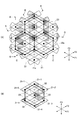
- FIG. 2 is a plan view (part 1) schematically showing irregularities on the surface of the antireflection structure of FIG.
- FIG. 2A shows an array of lattices connecting the vertices of the convex portions
- FIG. 2B shows a part of FIG.
- FIG. 3 is a view showing irregularities on the surface of the antireflection structure of FIG. 1.
- 3A is unevenness in the cross section along line AA in FIG. 2
- FIG. 3B is unevenness in the cross section along line BB in FIG. 2
- FIG. 3C is C in FIG.
- FIG. 3D shows unevenness in the cross section along the line DD in FIG. 2
- FIG. 3D shows unevenness in the cross section along the line DD in FIG.
- the antireflection structure 10 is a so-called moth-eye structure, and includes a base 12 and a resin layer 14 formed on the base 12 as shown in FIG.
- the base 12 and the resin layer 14 may have translucency.
- Periodic uneven portions 20 are formed on the surface of the resin layer 14.
- the antireflection structure 10 may be configured by only the resin layer 14.
- the base 12 is formed in a sheet shape, a plate shape, or a block shape, for example.
- substrate 12 is not specifically limited, For example, glass or a plastics etc. are used.
- soda lime glass for example, soda lime glass, non-alkali glass, quartz glass or the like is used.
- a glass forming method for example, a float method, a fusion method or the like is used.
- plastics include (meth) acrylic resins such as polymethyl methacrylate, methyl methacrylate and other alkyl (meth) acrylates, and copolymers of vinyl monomers such as styrene; polycarbonate, diethylene glycol bisallyl carbonate (CR-39) (Brominated) bisphenol A type di (meth) acrylate homopolymer or copolymer, (brominated) polymer of urethane-modified monomer of bisphenol A mono (meth) acrylate and copolymer Thermosetting (meth) acrylic resins such as coalescence; polyesters, especially polyethylene terephthalate, polyethylene naphthalate and unsaturated polyesters, acrylonitrile-styrene copolymers, polyvinyl chloride, polyurethane Epoxy resins, polyarylate, polyether sulfone, polyether ketone, cycloolefin polymer (trade name: ARTON, ZEONOR) and the like are prefer
- the resin layer 14 is formed by, for example, applying and curing a thermosetting or photocurable resin on the base 12.
- An uneven portion 20 is formed on the surface of the resin layer 14.
- the concavo-convex portion 20 is formed between the predetermined convex portions 21 at a position lower than the convex portion 21, the concave portion 22, and the vertex 22 a of the convex portion 21 and higher than the bottom point 22 a of the concave portion 22.
- a connecting portion 23 for connecting the two A plurality of convex portions 21, a plurality of concave portions 22, and a plurality of connecting portions 23 are two-dimensionally arranged.
- the convex portions 21 are periodically arranged in, for example, a regular hexagonal lattice shape, a quasi-hexagonal lattice shape, a regular tetragonal lattice shape, or a quasi-tetragonal lattice shape (a regular hexagonal lattice shape in FIGS. 1 and 2).
- the convex portions 21 are preferably periodically arranged in a hexagonal lattice shape.
- a case where the convex portions 21 are periodically arranged in a hexagonal lattice shape will be described. Note that the case where the convex portions 21 are periodically arranged in a tetragonal lattice pattern will be described in the second embodiment.
- “Periodically arranged in a regular hexagonal lattice shape” means that, as shown in FIG. 2, the arbitrary convex portions 21-1 are arranged around the arbitrary convex portions 21-1 excluding the outermost convex portions 21. This means that six convex portions 21-2 to 21-7 having the shortest distance and the same distance are arranged. The vertices of the six convex portions 21-2 to 21-7 are arranged at an equal pitch at an interval of 60 ° with the vertex of the convex portion 21-1 as the center, and constitute a regular hexagonal lattice.
- “To be periodically arranged in a quasi-hexagonal lattice shape” means to be periodically arranged in a shape according to a regular hexagonal lattice.
- the shape conforming to the regular hexagonal lattice is a shape obtained by distorting a regular hexagonal lattice such as a shape obtained by stretching a regular hexagonal lattice in a predetermined direction.
- a lattice having a shape obtained by distorting a regular hexagonal lattice may be continuously arranged in a linear shape, a curved shape, or a meandering shape.
- convex portions 21-1 there are six convex portions 21-1 excluding the outermost convex portion 21 and the total (sum) of the distances from the convex portions 21-1 that is the shortest.
- the convex portions 21-2 to 21-7 are arranged so as to satisfy the following conditions (1) and (2).
- (1) Between the four convex portions 21-2, 21-3, 21-5, 21-6 of the six convex portions 21-2 to 21-7 and the convex portion 21-1.
- a concave portion 22 exists between each of the remaining two convex portions 21-4 and 21-7 among the six convex portions 21-2 to 21-7 and the convex portion 21-1. .
- “Distance” is the distance between the vertices 21 a of the convex portions 21.
- Concave portions 22 and connecting portions 23 are alternately arranged along a direction parallel to the F1 direction (see FIGS. 2 and 3D).
- the direction in which the convex portions 21 and the concave portions 22 are alternately arranged is different from the direction in which the convex portions 21 and the connecting portions 23 are alternately arranged. Therefore, the height difference H1 (see FIG. 3B) between the vertex 21a of the convex portion 21 and the bottom point 22a of the concave portion 22, and the vertex 21a of the convex portion 21 and the predetermined portion 23a of the connecting portion 23 (see FIG. 1).
- the height difference H2 (see FIG. 3A) can be designed independently. Therefore, the height difference H1 and the height difference H2 can be optimized independently.
- the predetermined portion 23 a of the connecting portion 23 is the lowest portion between the vertices 21 a of the convex portions 21 and is the highest portion between the bottom points 22 a of the concave portions 22.
- the range of the pitch P1 may be set.
- the pitch P1 is set to a length equal to or shorter than the wavelength of visible light, and may be, for example, 400 nm or less (preferably 300 nm or less). Further, the pitch P1 may be, for example, 50 nm or more (preferably 100 nm or more) from the viewpoint of productivity. Therefore, the pitch P1 may be 50 nm to 400 nm.
- the aspect ratio of the concavo-convex portion 20 is represented by a ratio H1 / P1 between the height difference H1 between the apex 21a of the convex portion 21 and the bottom point 22a of the concave portion 22 and the pitch P1 of the convex portion 21.
- the aspect ratio H1 / P1 is, for example, 0.5 or more (preferably 0.7 or more, more preferably 1 or more) from the viewpoint of low reflectivity of the antireflection structure 10.
- the aspect ratio H1 / P1 is, for example, 4 or less (preferably 3 or less, more preferably 2 or less) from the viewpoint of productivity.
- the aspect ratio is obtained with the shortest pitch. Since the aspect ratio H1 / P1 is 0.5 to 4, the height difference H1 may be, for example, 100 nm to 500 nm.
- a ratio H2 / H1 between the height difference H1 and the height difference H2 is set.
- the ratio H2 / H1 increases, the height of the predetermined portion 23a of the connecting portion 23 decreases, so that the low reflectivity of the antireflection structure 10 is improved.
- the ratio H2 / H1 is, for example, 0.1 or more (preferably 0.2 or more, more preferably 0.3 or more).
- the ratio H2 / H1 is decreased, the height of the predetermined portion 23a of the connecting portion 23 is increased and the convex portion 21 is reinforced, so that the anti-reflection structure 10 has better scratch resistance.
- the ratio H2 / H1 is, for example, 0.9 or less (preferably 0.7 or less, more preferably 0.5 or less). Since the ratio H2 / H1 is 0.1 to 0.9, the height difference H2 may be, for example, 30 nm to 300 nm.
- the aspect ratio H1 / P1 and the ratio H2 / H1 can be optimized independently. Both low reflectivity and scratch resistance are possible.
- the pitch P1, the height difference H1, the height difference H2, and the like are obtained from an AFM image taken with an atomic force microscope (AFM) and a cross-sectional profile thereof.
- AFM atomic force microscope
- the convex portions 21 and the connecting portions 23 are alternately arranged along the F1 direction and the F2 direction which are linear directions, and the convex portions 21 and the concave portions 22 are arranged along the F3 direction which is a linear direction.
- the present invention is not limited to this as long as the above conditions (1) and (2) are satisfied.
- the convex portions 21 and the connecting portions 23 may be alternately arranged along a predetermined curved direction.
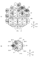
- FIG. 4 is a plan view (part 2) schematically showing irregularities on the surface of the antireflection structure of FIG.
- FIG. 4A shows an array of grids connecting the bottoms of the recesses
- FIG. 4B shows a part of FIG.
- the convex portions and the connecting portions are indicated by different dot patterns
- the vertexes of the convex portions are black circles
- the bottom points of the concave portions are white circles
- the grids connecting the bottom points of the concave portions are indicated by bold lines.
- an arbitrary recess 22-1 excluding the outermost recess 22 and six recesses 22-2 to 22-7 whose sum (sum) of distances from the recess 22-1 is the shortest. Is arranged so as to satisfy the following conditions (3) and (4).
- 23 exists.
- a convex portion 21 exists between each of the remaining two concave portions 22-4 and 22-7 among the six concave portions 22-2 to 22-7 and the concave portion 22-1.
- “Distance” is the distance between the bottom points 22 a of the recesses 22.
- FIG. 5 and 6 are explanatory views (No. 1) and (No. 2) of the method of manufacturing the antireflection structure according to the first embodiment of the present invention.
- FIG. 5 shows a first step of producing a stamper using a prototype
- FIG. 6 shows a second step of producing an antireflection structure using a stamper.
- the manufacturing method of the antireflection structure includes a step of manufacturing the antireflection structure 10 having the periodic uneven portions 20 on the surface by using the prototype 50 having the periodic uneven portions 60 on the surface.
- the step includes, for example, a first step of producing a stamper 70 having a concavo-convex portion 80 on the surface of which the shape of the concavo-convex portion 60 of the prototype 50 is reversed, and a concavo-convex portion obtained by reversing and transferring the shape of the concavo-convex portion 80 of the stamper 70.
- a second step of producing the antireflection structure 10 having 20 on the surface The prototype 50 can be used repeatedly in the first step, and the stamper 70 can be used repeatedly in the second step.
- the first step includes, for example, a step of preparing the prototype 50 (see FIG. 5A), and a step of manufacturing the stamper 70 by forming a metal film on the uneven portion 60 of the prototype 50 (FIG. 5B). And a step of peeling the stamper 70 from the master 50 (see FIG. 5C).
- the stamper 70 is formed, for example, by forming a conductive film on the concavo-convex portion 60 of the prototype 50 and then forming a metal film such as Ni on the conductive film by electroforming.
- PVD methods such as electroless plating, sputtering, and vacuum deposition are used.
- the second step for example, a step of applying a curable resin onto the base 12 (see FIG. 6A), and the coating layer 13 is cured in a state where the uneven portion 80 of the stamper 70 is pressed against the surface of the coating layer 13. And a step of peeling the stamper 70 from the resin layer 14 formed by curing the coating layer 13 (see FIG. 6C).
- a curable resin for example, a thermosetting resin or a photocurable resin is used.
- a method for applying the curable resin for example, a general method such as a spin coating method, a die coating method, or an ink jet method is used.
- the antireflection structure 10 is manufactured. Since the uneven portion 20 of the antireflection structure 10 has a shape obtained by inverting the shape of the uneven portion 60 of the prototype 50 twice, it has substantially the same shape and substantially the same dimensions as the uneven portion 60 of the prototype 50.
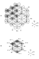
- FIG. 7 is a plan view schematically showing irregularities on the surface of the prototype of FIG.
- FIG. 7A shows an array of lattices connecting the vertices of the convex portions
- FIG. 7B shows a part of FIG.
- the convex portions and the connecting portions are indicated by different dot patterns
- the vertexes of the convex portions are indicated by black circles
- the bottom points of the concave portions are indicated by white circles
- the grids connecting the vertexes of the convex portions are indicated by bold lines.
- the concavo-convex part 60 of the prototype 50 is lower than the convex part 61, the concave part 62, and the apex 61 a of the convex part 61, as in the concave-convex part 20 of the antireflection structure 10. It has the connection part 63 which connects predetermined convex parts 61 in the position higher than the point 62a.
- a plurality of convex portions 61, a plurality of concave portions 62, and a plurality of connecting portions 63 are two-dimensionally arranged.
- the convex portions 61 are periodically arranged in, for example, a regular hexagonal lattice shape, a quasi-hexagonal lattice shape, a regular tetragonal lattice shape, or a quasi-tetragonal lattice shape (in this embodiment, a regular hexagonal lattice shape).
- the convex portions 61 are preferably arranged periodically in a hexagonal lattice shape.
- the distance from the arbitrary convex portion 61-1 around the arbitrary convex portion 61-1 except the outermost convex portion 61 is the shortest.
- equal six convex portions 61-2 to 61-7 are arranged.
- the vertices of the six convex portions 61-2 to 61-7 are arranged at an equal pitch with an interval of 60 ° around the vertex of the convex portion 61-1, and constitute a regular hexagonal lattice.
- the convex portions 61-2 to 61-7 are arranged so as to satisfy the following conditions (5) and (6).
- (5) Between the four convex portions 61-2, 61-3, 61-5, 61-6 of the six convex portions 61-2 to 61-7 and the convex portion 61-1.
- a concave portion 62 exists between each of the remaining two convex portions 61-4 and 61-7 among the six convex portions 61-2 to 61-7 and the convex portion 61-1. .
- the projection 61 is connected along two directions (F1 direction and F2 direction) among the three directions intersecting with an arbitrary projection 61-1.
- the portions 63 are alternately arranged, and the convex portions 61 and the concave portions 62 are alternately arranged along the remaining one direction (F3 direction).
- Concave portions 62 and connecting portions 63 are alternately arranged along a direction parallel to the F1 direction.
- the direction in which the convex portions 61 and the concave portions 62 are alternately arranged differs from the direction in which the convex portions 61 and the connecting portions 63 are alternately arranged. Therefore, the height difference between the apex 61a of the convex portion 61 and the bottom point 62a of the concave portion 62, and the predetermined portion of the apex 61a of the convex portion 61 and the connecting portion 63 (corresponding to the predetermined portion 23a of the connecting portion 23 of the antireflection structure 10). It is possible to design the difference in height with respect to the portion). Accordingly, in the antireflection structure 10 shown in FIGS.
- the height difference H2 can be designed independently. Therefore, since the height difference H1 and the height difference H2 can be optimized independently, both low reflectivity and scratch resistance can be achieved.
- the concavo-convex portion 20 of the antireflection structure 10 has a shape obtained by inverting the shape of the concavo-convex portion 60 of the prototype 50 twice, but the shape of the concavo-convex portion 60 of the prototype 50 is inverted one or more times. It is only necessary to have a shape, and the coating layer 13 may be cured in a state in which the uneven portion 60 of the prototype 50 is pressed against the surface of the coating layer 13 (see FIG. 6). Regardless of the number of times of reversal transfer, the convex portion 21 of the antireflection structure 10 satisfies the above conditions (1) and (2), so that both low reflectivity and scratch resistance can be achieved.
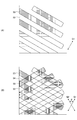
- FIG. 8 is an explanatory diagram (part 3) of the method for manufacturing the antireflection structure according to the first embodiment of the present invention.
- FIG. 8 shows a process of manufacturing a prototype.
- the method for manufacturing the antireflection structure may further include a step of manufacturing the prototype 50.
- This step includes, for example, a step of forming a resist film 52 on the substrate 51 (see FIGS. 5 and 6), and a step of changing the light intensity on the surface of the resist film 52 in the first direction (G1 direction).
- a step of exposing one interference fringe see FIG. 8A
- a second interference whose light intensity changes on the surface of the resist film 52 in a second direction (G2 direction) intersecting the first direction.
- a step of exposing the stripes see FIG. 8B) and a step of developing the resist film 52 after the exposure of the first and second interference fringes.
- the substrate 51 (see FIGS. 5 and 6) is formed in a sheet shape, a plate shape, a block shape, or a roll shape, for example.
- substrate 51 is not specifically limited, For example, a silicon
- the material of the resist film 52 a general material is used, and either a negative type or a positive type can be used. A developing solution is selected according to the material of the resist film 52.
- the first interference fringes are formed by the two-beam interference exposure method.
- a plurality of photosensitive portions 53 exposed by the first interference fringes are arranged at intervals in the first direction (G1 direction).
- a general laser oscillator such as a He—Cd laser (wavelength: 325 nm) is used.
- the second interference fringes are formed by the two-beam interference exposure method in the same manner as the first interference fringes after the resist film 52 is rotated.
- a plurality of photosensitive portions 54 exposed by the first interference fringes are arranged at intervals in the second direction (G2 direction).
- the exposure of the first interference fringes and the exposure of the second interference fringes are performed separately, but may be performed simultaneously.
- the development of the resist film 52 is performed after the exposure of the first and second interference fringes.
- a resin layer 56 (see FIG. 5A) having periodic uneven portions 60 on the surface is obtained.
- the intersection 55 between the photosensitive portion 53 and the photosensitive portion 54 becomes the convex portion 61 after development.
- the convex portion 61 is formed in a tapered shape toward the vertex 61a.
- the portions other than the intersecting portion 55 of the photosensitive portions 53 and 54 become the connecting portion 63 after development.
- a crossing portion 55 between the photosensitive portion 53 and the photosensitive portion 54 becomes a concave portion 62 after development.
- the recess 62 is formed in a tapered shape toward the bottom point 62a. The portions other than the intersecting portion 55 of the photosensitive portions 53 and 54 become the connecting portion 63 after development.
- the prototype 50 is produced.
- the angle ⁇ formed by the first direction and the second direction is 60 °
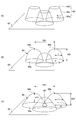
- the convex portions 61 are periodically arranged in a regular hexagonal lattice shape.
- the angle ⁇ formed by the first direction and the second direction is 90 °
- the convex portions 61 are periodically arranged in a regular tetragonal lattice shape.
- the prototype 50 of this embodiment is produced by exposing the interference fringes to the resist film 52 by the two-beam interference exposure method
- the production method of the prototype 50 is not particularly limited.
- the concavo-convex portion 60 may be formed on the surface of the substrate 51 by photolithography, electron beam (EB) drawing, laser drawing, or the like.
- FIG. 9 is a perspective view showing a part of the antireflection structure according to the second embodiment of the present invention.
- contour lines are shown by thin lines in order to express irregularities on the surface of the antireflection structure.
- FIG. 10 is a plan view schematically showing irregularities on the surface of the antireflection structure of FIG.
- FIG. 10A shows an array of lattices connecting the vertices of the convex portions
- FIG. 10B shows a part of FIG.
- FIG. 11 is a view showing irregularities on the surface of the antireflection structure of FIG. 9.
- 11A is unevenness in the cross section along line AA in FIG. 10
- FIG. 11B is unevenness in the cross section along line BB in FIG. 10
- FIG. 11C is C in FIG. Shows irregularities in the cross section along the line -C.
- the antireflection structure 110 is of a so-called moth-eye type, and is composed of a base 112 and a resin layer 114 formed on the base 112 as in the first embodiment, as shown in FIG. Periodic uneven portions 120 are formed on the surface of the resin layer 114. Note that the antireflection structure 110 may be formed of only the resin layer 114.
- the concavo-convex portion 120 includes a convex portion 121, a concave portion 122, and a connecting portion 123 that couples the predetermined convex portions 121 to each other at a position lower than the vertex 121 a of the convex portion 121 and higher than the bottom point 122 a of the concave portion 122.
- a plurality of convex portions 121, a plurality of concave portions 122, and a plurality of connecting portions 123 are two-dimensionally arranged.
- the convex portions 121 are periodically arranged in a regular tetragonal lattice shape, for example. “Periodically arranged in the form of a tetragonal lattice” means that, as shown in FIG. 10, the distance from any recess 122 is shortest around any recess 122 except the outermost recess 122. It means that four equal convex portions 121 are arranged. The vertices 121a of the four convex portions 121 are arranged at equal pitches at 90 ° intervals around the bottom point 122a of the concave portion 122, and constitute a regular tetragonal lattice.
- the convex portions 121 may be periodically arranged in a quasi-tetragonal lattice shape.
- “Periodically arranged in a quasi-tetragonal lattice shape” means periodically arranged in a shape that conforms to a regular tetragonal lattice.
- the shape conforming to the tetragonal lattice is a shape obtained by distorting a regular tetragonal lattice such as a shape obtained by stretching a regular tetragonal lattice in a predetermined direction.
- a lattice having a shape obtained by distorting a regular tetragonal lattice may be continuously arranged in a linear shape, a curved shape, or a meandering shape.
- convex portions 121-1 there are six convex parts 121-1 excluding the outermost convex part 121, and the total (sum) of the distances from the convex parts 121-1 that is the shortest.
- the convex portions (for example, convex portions 121-2 to 121-7) are arranged so as to satisfy the following conditions (7) and (8).
- (7) Between the four convex portions 121-2, 121-3, 121-5, 121-6 of the six convex portions 121-2 to 121-7 and the convex portion 121-1.
- a concave portion 122 exists between each of the remaining two convex portions 121-4 and 121-7 among the six convex portions 121-2 to 121-7 and the convex portion 121-1. .
- “Distance” is the distance between the vertices 121 a of the convex portions 121.
- the above conditions (7) and (8) are satisfied for all combinations.
- the projection 121 is connected along two directions (the J1 direction and the J2 direction) among the three directions intersecting around the arbitrary projection 121-1.
- the portions 123 are alternately arranged, and the convex portions 121 and the concave portions 122 are alternately arranged along the remaining one direction (J3 direction).
- the pitch P11 (see FIG. 11A) of the protrusions 121 arranged at intervals in the J1 direction and the J2 direction may be set to a length equal to or shorter than the wavelength of visible light.
- the pitch P12 (see FIG. 11B) of the protrusions 121 arranged at intervals in the J3 direction is larger than the pitch P11.
- Concave portions 122 and connecting portions 123 are alternately arranged along a direction parallel to the J1 direction (see FIGS. 10 and 11C).
- the direction in which the convex portions 121 and the concave portions 122 are alternately arranged is different from the direction in which the convex portions 121 and the connecting portions 123 are alternately arranged. Therefore, the height difference H11 (see FIG. 11B) between the vertex 121a of the convex portion 121 and the bottom point 122a of the concave portion 122, the vertex 121a of the convex portion 121, and the predetermined portion 123a of the connecting portion 123 (see FIG. 9).
- the height difference H12 (see FIG. 11A) can be designed independently. Therefore, the height difference H11 and the height difference H12 can be optimized independently.
- the predetermined portion 123 a of the connecting portion 123 is the lowest portion between the vertices 121 a of the convex portions 121 and the highest portion between the bottom points 122 a of the concave portions 122.
- the range of the pitch P11 may be set. Since the pitch P11 is set to a length equal to or shorter than the wavelength of visible light as described above, the pitch P11 may be, for example, 400 nm or less (preferably 300 nm or less). Further, the pitch P11 may be, for example, 50 nm or more (preferably 100 nm or more) from the viewpoint of productivity. Therefore, the pitch P11 may be 50 nm to 400 nm.
- the aspect ratio of the concavo-convex portion 120 is represented by a ratio H11 / P11 between the height difference H11 between the apex 121a of the convex portion 121 and the bottom point 122a of the concave portion 122 and the pitch P11 of the convex portion 121.
- the aspect ratio H11 / P11 is, for example, 0.5 or more (preferably 0.7 or more, more preferably 1 or more) from the viewpoint of low reflectivity of the antireflection structure 110.
- the aspect ratio H11 / P11 is, for example, 4 or less (preferably 3 or less, more preferably 2 or less) from the viewpoint of productivity.
- the aspect ratio is obtained with the shortest pitch. Since the aspect ratio H11 / P11 is 0.5 to 4, the height difference H11 may be, for example, 100 nm to 500 nm.
- the ratio H12 / H11 between the height difference H11 and the height difference H12 is set.
- the ratio H12 / H11 increases, the height of the predetermined portion 123a of the connecting portion 123 decreases, so that the low reflectivity of the antireflection structure 110 improves.
- the ratio H12 / H11 is, for example, 0.1 or more (preferably 0.2 or more, more preferably 0.3 or more).
- the ratio H12 / H11 decreases, the height of the predetermined portion 123a of the connecting portion 123 increases and the convex portion 121 is reinforced, so that the anti-reflection structure 110 has better scratch resistance.
- the ratio H12 / H11 is, for example, 0.9 or less (preferably 0.7 or less, more preferably 0.5 or less). Since the ratio H12 / H11 is 0.1 to 0.9, the height difference H12 may be, for example, 30 nm to 300 nm.
- the aspect ratio H11 / P11 and the ratio H12 / H11 can be optimized independently. Both low reflectivity and scratch resistance are possible.
- the manufacturing method of the antireflection structure 110 having the above configuration is the same as the manufacturing method of the antireflection structure 10 according to the first embodiment, the description thereof will be omitted.
- a low-reflection layer may be provided on the back surface of the antireflection structure (the surface opposite to the surface on which the moth-eye type irregularities are formed).
- the low reflection layer has translucency.
- the low reflection layer may reduce the reflectance by the interference action of light, or may reduce the reflectance by absorption of light.
- the low reflection layer is formed of an organic material and / or an inorganic material.
- dry coating such as PVD method or CVD method
- wet coating such as die coating method, spray coating method, ink jet method or spin coating method is used.
- the antireflection structure is used for a touch panel, the low reflection layer may be disposed on the outside, and the moth-eye type uneven portion may be disposed on the inside.
- the convex part of the said embodiment is tapering toward the top, the convex part may have a flat top part.
- the “distance” in the claims is the distance between the center points of the tops of the convex portions.
- the recessed part of the said embodiment is tapered toward the bottom point, the recessed part may have a flat bottom part.
- Example 1 In Example 1, a model for analysis of the antireflection structure having the uneven portions shown in FIGS. 1 to 3 was prepared, and simulation analysis was performed using a computer.
- the analysis model was produced by overlapping two ridge portions 91 having a sinusoidal cross section on a virtual plane 92 (only one is shown in FIG. 12). It is considered that when the interference fringes are exposed to the resist film once and developed, an uneven surface having a sinusoidal cross section is formed.
- the overlapping portion of the two protruding strip group 91 corresponds to the protruding portion 21 shown in FIGS.
- the crossing angle of the two convex stripe groups 91 was set to 60 ° so that the convex portions were periodically arranged in a regular hexagonal lattice pattern.
- the height difference H1 see FIG.
- the reflectance on the concavo-convex portion of the analysis model was analyzed by the FDTD method (finite difference time domain method). Cybernet's "Pointing For For Optics" was used as the analysis software.
- the result of the analysis is shown in FIG. In FIG. 14, the horizontal axis represents the light wavelength, and the vertical axis represents the light reflectance.
- L1 represents the analysis result of Example 1
- L11 to L13 represent the analysis results of Comparative Examples 1 to 3 described later.
- the surface of the substrate having a thickness of 0.7 ⁇ m was used instead of the virtual plane 92.
- the physical property value (for example, the refractive index) of the substrate the physical property value of the acrylic resin was used in the same manner as the physical property value of the protruding strip group 91.
- the scratch resistance of the analytical model As the scratch resistance of the analytical model, the maximum stress generated in the convex portion when an external force in the direction perpendicular to the height direction of each convex portion is applied to the vertex of each convex portion was analyzed by the finite element method. As the analysis software, “Solid Works Simulation” manufactured by Solid Works was used. A smaller maximum stress means higher scratch resistance. Table 1 shows the relative value of the maximum stress (the maximum stress of Comparative Example 1 described later is 1). The reason for the relative value is that the length of the model for stress analysis (for example, height difference H1, H2, pitch P1, etc.) is set to 1000 times the actual length due to software restrictions.
- Comparative Example 1 In Comparative Example 1, a model for analysis of an antireflection structure having a concavo-convex portion similar to the conventional one was produced, and simulation analysis was performed using a computer in the same manner as in Example 1.
- the analysis model is arranged on the virtual plane 92 periodically in a regular hexagonal lattice pattern at a pitch of 250 nm (see FIG. 13A, in FIG. 13). Only the three truncated cones 93 are shown), and the corners of the top surface 93b and the tapered surface 93c of each truncated cone 93 are rounded, and the tip portion is formed by a protrusion 94 composed of a part of a spherical surface (FIG. 13). (See (B)).
- the height (the height difference between the bottom surface 94a and the apex 94b) H21 of the protrusion 94 was set to 300 nm, and the pitch P21 of the apex 94b of the protrusion 94 was set to 250 nm.
- the radius R of the bottom surface 94a was set to 120 nm so that the bottom surfaces 94a of the protrusions 94 were separated from each other.
- the radius r of the cut surface when the protrusion 94 was cut at the center in the height direction was 94 nm.
- An angle ⁇ (see FIG. 13A) formed by the bottom surface 93a of the truncated cone 93 and the tapered surface 93c was set to 80 °.
- the physical property values (for example, refractive index and Young's modulus) of the protrusions 94 the physical property values of acrylic resin were used.
- FIG. 14 shows the analysis result of the light reflectance
- Table 1 shows the analysis result of the stress.
- Comparative Example 2 In Comparative Example 2, the angle ⁇ (see FIG. 13A) formed by the bottom surface 93a of the truncated cone 93 and the tapered surface 93c is 70 °, the radius R of the bottom surface 94a of the protrusion 94 is 150 nm, and FIG.
- the analysis model of the antireflection structure is produced in the same manner as in Comparative Example 1 except that the bottom surfaces 94a of the protrusions 94 are partially overlapped to form the flanges 95 between the apexes 94b of the protrusions 94 as shown in FIG. In the same manner as in Example 1, simulation analysis was performed using a computer.
- the height difference H22 between the apex 94b of the protrusion 94 and the flange 95 is 160 nm, and the radius r of the cut surface when the protrusion 94 is cut at the center in the height direction is 124 nm.
- FIG. 14 shows the analysis result of the light reflectance, and Table 1 shows the analysis result of the stress.
- Comparative Example 3 In Comparative Example 3, the height difference H22 between the apex 94b of the protrusion 94 and the flange 95 is set by setting the angle ⁇ (see FIG. 13A) formed by the bottom surface 93a of the truncated cone 93 and the tapered surface 93c to 80 °.
- An analysis model of the antireflection structure was prepared in the same manner as in Comparative Example 2 except that the thickness was set to 230 nm, and simulation analysis was performed using a computer in the same manner as in Example 1. The radius r of the cut surface when the protrusion 94 was cut at the center in the height direction was 95 nm.
- FIG. 14 shows the analysis result of the light reflectance
- Table 1 shows the analysis result of the stress.
- Example 1 has both low reflectivity and scratch resistance unlike the structures of Comparative Examples 1 to 3.
- Comparative Example 1 since the bottom surfaces 94a of the protrusions 94 are separated from each other and the flange portion 95 is not formed, the scratch resistance is poor.
- Comparative Example 2 and Comparative Example 3 the uneven portion of the antireflection structure does not satisfy the above conditions (1) and (2), and the low reflectivity is poor.
- Comparative Example 2 and Comparative Example 3 the bottom surfaces 94a of the protrusions 94 partially overlap each other so that the flange portion 95 is formed. Therefore, the bottom point of the recess of the antireflection structure is separated from the virtual plane 92, and the bottom point of the recess This is because the difference in height between the top and the top of the convex portion becomes small.
- the present invention is suitable for an antireflection structure that can be used, for example, in a display device or a solar cell, and a method for manufacturing the antireflection structure.
Landscapes
- Physics & Mathematics (AREA)
- General Physics & Mathematics (AREA)
- Optics & Photonics (AREA)
- Surface Treatment Of Optical Elements (AREA)
- Liquid Crystal (AREA)
- Optical Elements Other Than Lenses (AREA)
Abstract
周期的な凹凸部20を表面に有する反射防止構造体10において、最外側の凸部21を除く任意の凸部21-1と、該任意の凸部21-1からの距離の合計が最短の6個の凸部21-2~21-7とは、(1)6個の凸部21-2~21-7のうちの4個の凸部21-2、21-3、21-5、21-6のそれぞれと任意の凸部21-1との間に凸部21の頂点21aよりも低く凹部22の底点22aよりも高い位置で凸部同士を連結する連結部23が存在し、(2)6個の凸部21-2~21-7のうちの残りの2個の凸部21-4、21-7のそれぞれと任意の凸部21-1との間に凹部22が存在するように配置される。
Description
本発明は、反射防止構造体、及び反射防止構造体の製造方法に関する。
近年、液晶ディスプレイ(LCD)等の表示装置や太陽電池向けに、周期的な凹凸部を表面に有する反射防止構造体が開発されている(例えば、特許文献1参照)。反射防止構造体は、所謂モスアイ(Moth Eye)型であって、凸部のピッチが可視光の波長以下のため、広い波長範囲で光反射率を低減し光透過率を向上することができる。
従来の反射防止構造体の凹凸部は、平面上に錐状の突起部が多数配列された構造を有する。突起部の充填率を高めるため、突起部は六方格子状又は四方格子状に周期的に配置される。
反射防止構造体の低反射性の向上を目的として、突起部の充填率をさらに高めるため、突起部の下部同士が重なり合うように配置されることがある。
しかしながら、突起部の下部同士が重なり過ぎると、凸部の頂点と凹部の底点との高低差が小さくなるので、却って低反射性に悪影響を及ぼす。
また、反射防止構造体は、表面に凹凸部を有するので、表面が擦れたときに傷付きやすいという問題もあった。
本発明は、上記課題に鑑みてなされたものであって、低反射性及び耐擦傷性に優れた反射防止構造体、及び反射防止構造体の製造方法の提供を目的とする。
上記目的を解決するため、本発明の一の態様による反射防止構造体は、
周期的な凹凸部を表面に有する反射防止構造体において、
最外側の凸部を除く任意の凸部と、該任意の凸部からの距離の合計が最短である6個の凸部とは、(1)該6個の凸部のうちの4個の前記凸部のそれぞれと前記任意の凸部との間に凸部の頂点よりも低く凹部の底点よりも高い位置で凸部同士を連結する連結部が存在し、(2)該6個の凸部のうちの残りの2個の前記凸部のそれぞれと前記任意の凸部との間に凹部が存在するように、配置されることを特徴とする。
周期的な凹凸部を表面に有する反射防止構造体において、
最外側の凸部を除く任意の凸部と、該任意の凸部からの距離の合計が最短である6個の凸部とは、(1)該6個の凸部のうちの4個の前記凸部のそれぞれと前記任意の凸部との間に凸部の頂点よりも低く凹部の底点よりも高い位置で凸部同士を連結する連結部が存在し、(2)該6個の凸部のうちの残りの2個の前記凸部のそれぞれと前記任意の凸部との間に凹部が存在するように、配置されることを特徴とする。
さらに、本発明の他の態様による反射防止構造体の製造方法は、
周期的な凹凸部を表面に有する原型を用いて、周期的な凹凸部を表面に有する反射防止構造体を製造する工程を有し、
前記原型において、最外側の凸部を除く任意の凸部と、該任意の凸部からの距離の合計が最短である6個の凸部とは、(1)該6個の凸部のうちの4個の前記凸部のそれぞれと前記任意の凸部との間に凸部の頂点よりも低く凹部の底点よりも高い位置で凸部同士を連結する連結部が存在し、(2)該6個の凸部のうちの残りの2個の前記凸部のそれぞれと前記任意の凸部との間に凹部が存在するように、配置されることを特徴とする。
周期的な凹凸部を表面に有する原型を用いて、周期的な凹凸部を表面に有する反射防止構造体を製造する工程を有し、
前記原型において、最外側の凸部を除く任意の凸部と、該任意の凸部からの距離の合計が最短である6個の凸部とは、(1)該6個の凸部のうちの4個の前記凸部のそれぞれと前記任意の凸部との間に凸部の頂点よりも低く凹部の底点よりも高い位置で凸部同士を連結する連結部が存在し、(2)該6個の凸部のうちの残りの2個の前記凸部のそれぞれと前記任意の凸部との間に凹部が存在するように、配置されることを特徴とする。
本発明によれば、低反射性及び耐擦傷性に優れた反射防止構造体、及び反射防止構造体の製造方法が提供される。
以下、本発明を実施するための形態について図面を参照して説明する。各図面において、同一の又は対応する構成については同一の又は対応する符号を付して説明を省略する。
[第1の実施形態]
図1は、本発明の第1の実施形態による反射防止構造体の一部を示す斜視図である。図1において、反射防止構造体の表面の凹凸を表現するため、等高線を細線で示す。図2は、図1の反射防止構造体の表面の凹凸を模式的に示す平面図(その1)である。図2(A)は凸部の頂点を結ぶ格子の配列を示し、図2(B)は図2(A)の一部を示す。図2において、図面を見やすくするため、凸部及び連結部を異なる点模様、凸部の頂点を黒丸、凹部の底点を白丸、凸部の頂点を結ぶ格子を太線で示す。図3は、図1の反射防止構造体の表面の凹凸を示す図である。図3(A)は図2のA-A線に沿った断面における凹凸、図3(B)は図2のB-B線に沿った断面における凹凸、図3(C)は図2のC-C線に沿った断面における凹凸、図3(D)は図2のD-D線に沿った断面における凹凸を示す。
図1は、本発明の第1の実施形態による反射防止構造体の一部を示す斜視図である。図1において、反射防止構造体の表面の凹凸を表現するため、等高線を細線で示す。図2は、図1の反射防止構造体の表面の凹凸を模式的に示す平面図(その1)である。図2(A)は凸部の頂点を結ぶ格子の配列を示し、図2(B)は図2(A)の一部を示す。図2において、図面を見やすくするため、凸部及び連結部を異なる点模様、凸部の頂点を黒丸、凹部の底点を白丸、凸部の頂点を結ぶ格子を太線で示す。図3は、図1の反射防止構造体の表面の凹凸を示す図である。図3(A)は図2のA-A線に沿った断面における凹凸、図3(B)は図2のB-B線に沿った断面における凹凸、図3(C)は図2のC-C線に沿った断面における凹凸、図3(D)は図2のD-D線に沿った断面における凹凸を示す。
反射防止構造体10は、所謂モスアイ型であって、図1に示すように、基体12と基体12上に形成される樹脂層14とで構成される。基体12及び樹脂層14は、透光性を有してもよい。樹脂層14の表面には、周期的な凹凸部20が形成されている。尚、反射防止構造体10は、樹脂層14のみで構成されてもよい。
基体12は、例えばシート状、板状、又はブロック状に形成される。基体12の材料は、特に限定されないが、例えばガラス又はプラスチック等が用いられる。
ガラスとしては、例えばソーダライムガラス、無アルカリガラス、石英ガラス等が用いられる。ガラスの成形方法としては、例えばフロート法、フュージョン法等が用いられる。
プラスチックとしては、例えばポリメチルメタアクリレート、メチルメタクリレートと他のアルキル(メタ)アクリレート、スチレンなどといったビニルモノマーとの共重合体などの(メタ)アクリル系樹脂;ポリカーボネート、ジエチレングリコールビスアリルカーボネート(CR-39)などのポリカーボネート系樹脂;(臭素化)ビスフェノールA型のジ(メタ)アクリレートの単独重合体ないし共重合体、(臭素化)ビスフェノールAモノ(メタ)アクリレートのウレタン変性モノマーの重合体及び共重合体などといった熱硬化性(メタ)アクリル系樹脂;ポリエステル特にポリエチレンテレフタレート、ポリエチレンナフタレート及び不飽和ポリエステル、アクリロニトリル-スチレン共重合体、ポリ塩化ビニル、ポリウレタン、エポキシ樹脂、ポリアリレート、ポリエーテルスルホン、ポリエーテルケトン、シクロオレフィンポリマー(商品名:アートン、ゼオノア)などが好ましい。また、耐熱性を考慮したアラミド系樹脂の使用も可能である。
樹脂層14は、例えば基体12上に熱硬化性又は光硬化性の樹脂を塗布し、硬化してなる。樹脂層14の表面には凹凸部20が形成される。
凹凸部20は、図1及び図2に示すように、凸部21と、凹部22と、凸部21の頂点21aよりも低く凹部22の底点22aよりも高い位置で所定の凸部21同士を連結する連結部23とを有する。複数の凸部21と、複数の凹部22と、複数の連結部23とが2次元的に配列されている。
凸部21は、例えば正六方格子状、準六方格子状、正四方格子状、又は準四方格子状(図1及び図2では正六方格子状)に周期的に配置される。凸部21の充填率を高めるため、凸部21は六方格子状に周期的に配置されることが好ましい。以下、凸部21が六方格子状に周期的に配置される場合について説明する。尚、凸部21が四方格子状に周期的に配置される場合については、第2の実施形態で説明する。
「正六方格子状に周期的に配置される」とは、図2に示すように、最外側の凸部21を除く任意の凸部21-1の周囲に、該任意の凸部21-1からの距離が最短で且つ等しい6個の凸部21-2~21-7が配置されることを意味する。6個の凸部21-2~21-7の頂点は、凸部21-1の頂点を中心に60°間隔で等ピッチで配置され、正六角形状の格子を構成する。
「準六方格子状に周期的に配置される」とは、正六方格子に準ずる形状に周期的に配置されることを意味する。正六方格子に準ずる形状は、正六角形状の格子を所定の方向に引き伸ばした形状等、正六角形状の格子を歪ませた形状である。正六角形状の格子を歪ませた形状の格子は、直線形状、曲線形状、又は蛇行形状に連続的に並んでもよい。
本実施形態では、図2に示すように、最外側の凸部21を除く任意の凸部21-1と、該凸部21-1からの距離の合計(和)が最短である6個の凸部21-2~21-7とは、下記の条件(1)及び(2)を満たすように配置される。
(1)6個の凸部21-2~21-7のうちの4個の凸部21-2、21-3、21-5、21-6のそれぞれと、凸部21-1との間に連結部23が存在する。
(2)6個の凸部21-2~21-7のうちの残りの2個の凸部21-4、21-7のそれぞれと、凸部21-1との間に凹部22が存在する。
(1)6個の凸部21-2~21-7のうちの4個の凸部21-2、21-3、21-5、21-6のそれぞれと、凸部21-1との間に連結部23が存在する。
(2)6個の凸部21-2~21-7のうちの残りの2個の凸部21-4、21-7のそれぞれと、凸部21-1との間に凹部22が存在する。
「距離」は、凸部21の頂点21a同士の間の距離のことである。距離の合計が最短である6個の凸部の組合せが複数有る場合、全ての組合せについて上記の条件(1)及び(2)が成立する。尚、本実施形態では、距離の合計が最短である6個の凸部の組合せは1つだけである。
上記の条件(1)及び(2)が成立する場合、図2に示すように、例えば任意の凸部21-1を中心に交差する3方向のうち、2方向(F1方向及びF2方向)に沿って凸部21と連結部23とが交互に配置され、残りの一方向(F3方向)に沿って凸部21と凹部22とが交互に配置される。F1方向、F2方向、及びF3に間隔をおいて並ぶ凸部21のピッチP1(図3(A)及び図3(B)参照)は、可視光の波長以下の長さに設定されてもよい。F3方向と垂直な方向に間隔をおいて並ぶ凸部21のピッチP2(図3(C)参照)は、ピッチP1よりも大きい。F1方向と平行な方向に沿って凹部22と連結部23とが交互に配置されている(図2及び図3(D)参照)。
このように、凸部21及び凹部22が交互に配置される方向と、凸部21及び連結部23が交互に配置される方向とが異なる。そのため、凸部21の頂点21aと凹部22の底点22aとの高低差H1(図3(B)参照)と、凸部21の頂点21aと連結部23の所定部分23a(図1参照)との高低差H2(図3(A)参照)とを独立に設計可能である。従って、高低差H1と、高低差H2とを独立に最適化することが可能である。ここで、連結部23の所定部分23aは、凸部21の頂点21a同士の間における最も低い部分であって、凹部22の底点22a同士の間における最も高い部分である。
高低差H1と高低差H2の最適化のため、先ず、ピッチP1の範囲が設定されてもよい。ピッチP1は、上述の如く、可視光の波長以下の長さに設定されるので、例えば400nm以下(好ましくは300nm以下)であってもよい。また、ピッチP1は、生産性の観点から、例えば50nm以上(好ましくは100nm以上)であってもよい。従って、ピッチP1は50nm~400nmであってもよい。
次いで、凹凸部20のアスペクト比の範囲が設定される。凹凸部20のアスペクト比は、凸部21の頂点21aと凹部22の底点22aとの高低差H1と、凸部21のピッチP1との比H1/P1で表される。アスペクト比H1/P1は、反射防止構造体10の低反射性の観点から、例えば0.5以上(好ましくは0.7以上、より好ましくは1以上)である。また、アスペクト比H1/P1は、生産性の観点から、例えば4以下(好ましくは3以下、より好ましくは2以下)である。尚、凸部21のF1方向におけるピッチと、凸部21のF2方向におけるピッチと、凸部21のF3方向におけるピッチとが異なる場合、最短のピッチでアスペクト比が求められる。アスペクト比H1/P1が0.5~4であるので、高低差H1は例えば100nm~500nmであってもよい。
次いで、高低差H1と高低差H2との比H2/H1が設定される。比H2/H1が大きくなるほど、連結部23の所定部分23aの高さが低くなるので、反射防止構造体10の低反射性が良くなる。比H2/H1は、例えば0.1以上(好ましくは0.2以上、より好ましくは0.3以上)である。一方、比H2/H1が小さくなるほど、連結部23の所定部分23aの高さが高くなり、凸部21が補強されるので、反射防止構造体10の耐擦傷性が良くなる。比H2/H1は、例えば0.9以下(好ましくは0.7以下、より好ましくは0.5以下)である。比H2/H1が0.1~0.9であるので、高低差H2は例えば30nm~300nmであってもよい。
本実施形態では、高低差H1と、高低差H2とを独立に最適化することが可能であるので、アスペクト比H1/P1と、比H2/H1を独立に最適化することが可能であり、低反射性と耐擦傷性の両立が可能である。
ピッチP1、高低差H1、高低差H2等は、原子間力顕微鏡(AFM:Atomic Force Microscope)により撮影したAFM画像、及びその断面プロファイルから求められる。
尚、本実施形態では、直線方向であるF1方向及びF2方向に沿って凸部21と連結部23とが交互に配列され、直線方向であるF3方向に沿って凸部21と凹部22とが交互に配列されるが、上記の条件(1)及び(2)が成立する限り、本発明はこれに限定されない。例えば、六角形状の格子を湾曲状に配列する場合、所定の曲線方向に沿って凸部21と連結部23とが交互に配列されてもよい。
尚、本実施形態では、凸部21の配置について着目したが、凹部22の配置について着目してもよい。
図4は、図1の反射防止構造体の表面の凹凸を模式的に示す平面図(その2)である。図4(A)は凹部の底点を結ぶ格子の配列を示し、図4(B)は図4(A)の一部を示す。図4において、図面を見やすくするため、凸部及び連結部を異なる点模様、凸部の頂点を黒丸、凹部の底点を白丸、凹部の底点を結ぶ格子を太線で示す。
図4に示すように、最外側の凹部22を除く任意の凹部22-1と、該凹部22-1からの距離の合計(和)が最短である6個の凹部22-2~22-7とは、下記の条件(3)及び(4)を満たすように配置される。
(3)6個の凹部22-2~22-7のうちの4個の凹部22-2、22-3、22-5、22-6のそれぞれと、凹部22-1との間に連結部23が存在する。
(4)6個の凹部22-2~22-7のうちの残りの2個の凹部22-4、22-7のそれぞれと、凹部22-1との間に凸部21が存在する。
(3)6個の凹部22-2~22-7のうちの4個の凹部22-2、22-3、22-5、22-6のそれぞれと、凹部22-1との間に連結部23が存在する。
(4)6個の凹部22-2~22-7のうちの残りの2個の凹部22-4、22-7のそれぞれと、凹部22-1との間に凸部21が存在する。
「距離」は、凹部22の底点22a同士の間の距離のことである。距離の合計が最短である6個の凹部22の組合せが複数有る場合、全ての組合せについて上記の条件(3)及び(4)が成立する。本実施形態では、距離の合計が最短である6個の凹部22の組合せは1つだけである。
図5及び図6は、本発明の第1の実施形態による反射防止構造体の製造方法の説明図(その1)及び(その2)である。図5は原型を用いてスタンパを作製する第1の工程を示し、図6はスタンパを用いて反射防止構造体を作製する第2の工程を示す。
反射防止構造体の製造方法は、周期的な凹凸部60を表面に有する原型50を用いて、周期的な凹凸部20を表面に有する反射防止構造体10を製造する工程を有する。該工程は、例えば、原型50の凹凸部60の形状を反転転写した凹凸部80を表面に有するスタンパ70を作製する第1の工程と、スタンパ70の凹凸部80の形状を反転転写した凹凸部20を表面に有する反射防止構造体10を作製する第2の工程とを有する。原型50は第1の工程において繰り返し使用可能であり、スタンパ70は第2の工程において繰り返し使用可能である。
第1の工程は、例えば、原型50を用意する工程(図5(A)参照)と、原型50の凹凸部60上に金属膜を成膜してスタンパ70を作製する工程(図5(B)参照)と、スタンパ70を原型50から剥離する工程(図5(C)参照)とを有する。スタンパ70は、例えば原型50の凹凸部60上に導電膜を形成した後、導電膜上にNi等の金属膜を電鋳法で形成してなる。導電膜の形成方法としては、無電解メッキ、スパッタリングや真空蒸着等のPVD法が用いられる。
第2の工程は、例えば基体12上に硬化性樹脂を塗布する工程(図6(A)参照)と、塗布層13の表面にスタンパ70の凹凸部80を押し付けた状態で塗布層13を硬化する工程(図6(B)参照)と、塗布層13を硬化してなる樹脂層14からスタンパ70を剥離する工程(図6(C)参照)とを有する。硬化性樹脂には、例えば熱硬化性樹脂又は光硬化性樹脂が用いられる。硬化性樹脂の塗布方法としては、例えばスピンコート法、ダイコート法、インクジェット法等の一般的な方法が用いられる。
このようにして、反射防止構造体10が製造される。反射防止構造体10の凹凸部20は、原型50の凹凸部60の形状を2回反転した形状を有するので、原型50の凹凸部60と略同じ形状、略同じ寸法を有する。
図7は、図5の原型の表面の凹凸を模式的に示す平面図である。図7(A)は凸部の頂点を結ぶ格子の配列を示し、図7(B)は図7(A)の一部を示す。図7において、図面を見やすくするため、凸部及び連結部を異なる点模様、凸部の頂点を黒丸、凹部の底点を白丸、凸部の頂点を結ぶ格子を太線で示す。
原型50の凹凸部60は、反射防止構造体10の凹凸部20と同様に、図7に示すように、凸部61と、凹部62と、凸部61の頂点61aよりも低く凹部62の底点62aよりも高い位置で所定の凸部61同士を連結する連結部63とを有する。複数の凸部61と、複数の凹部62と、複数の連結部63とが2次元的に配列されている。
凸部61は、例えば正六方格子状、準六方格子状、正四方格子状、又は準四方格子状(本実施形態では正六方格子状)に周期的に配置される。凸部61の充填率を高めるため、凸部61は、六方格子状に周期的に配置されることが好ましい。
凸部61が正六方格子状に周期的に配置される場合、最外側の凸部61を除く任意の凸部61-1の周囲に、該任意の凸部61-1からの距離が最短で且つ等しい6個の凸部61-2~61-7が配置される。6個の凸部61-2~61-7の頂点は、凸部61-1の頂点を中心に60°間隔で等ピッチで配置され、正六角形状の格子を構成する。
本実施形態では、図7に示すように、最外側の凸部61を除く任意の凸部61-1と、該凸部61-1からの距離の合計(和)が最短である6個の凸部61-2~61-7とは、下記の条件(5)及び(6)を満たすように配置される。
(5)6個の凸部61-2~61-7のうちの4個の凸部61-2、61-3、61-5、61-6のそれぞれと、凸部61-1との間に連結部63が存在する。
(6)6個の凸部61-2~61-7のうちの残りの2個の凸部61-4、61-7のそれぞれと、凸部61-1との間に凹部62が存在する。
(5)6個の凸部61-2~61-7のうちの4個の凸部61-2、61-3、61-5、61-6のそれぞれと、凸部61-1との間に連結部63が存在する。
(6)6個の凸部61-2~61-7のうちの残りの2個の凸部61-4、61-7のそれぞれと、凸部61-1との間に凹部62が存在する。
尚、本実施形態では、距離の合計が最短である6個の凸部の組合せは1つだけである。
上記の条件(5)及び(6)が成立する場合、例えば任意の凸部61-1を中心に交差する3方向のうち、2方向(F1方向及びF2方向)に沿って凸部61と連結部63とが交互に配置され、残りの一方向(F3方向)に沿って凸部61と凹部62とが交互に配置される。F1方向と平行な方向に沿って、凹部62と連結部63とが交互に配置されている。
このように、原型50において、凸部61及び凹部62が交互に配置される方向と、凸部61及び連結部63が交互に配置される方向とが異なる。そのため、凸部61の頂点61aと凹部62の底点62aとの高低差と、凸部61の頂点61aと連結部63の所定部分(反射防止構造体10の連結部23の所定部分23aに対応する部分)との高低差とを独立に設計可能である。よって、図1~図4に示す反射防止構造体10において凸部21の頂点21aと凹部22の底点22aとの高低差H1と、凸部21の頂点21aと連結部23の所定部分23aとの高低差H2とを独立に設計可能である。よって、高低差H1と、高低差H2とを独立に最適化することが可能であるので、低反射性と耐擦傷性との両立が可能である。
尚、本実施形態では、反射防止構造体10の凹凸部20は、原型50の凹凸部60の形状を2回反転した形状を有するが、原型50の凹凸部60の形状を1回以上反転した形状を有していればよく、塗布層13(図6参照)の表面に原型50の凹凸部60を押し付けた状態で塗布層13を硬化してもよい。反転転写の回数に関係なく、反射防止構造体10の凸部21は上記の条件(1)及び(2)を満たすので、低反射性と耐擦傷性との両立が可能である。
図8は、本発明の第1の実施形態による反射防止構造体の製造方法の説明図(その3)である。図8は、原型を製造する工程を示す。
反射防止構造体の製造方法は、原型50を製造する工程をさらに有してもよい。該工程は、例えば、基体51(図5及び図6参照)上にレジスト膜52を成膜する工程と、レジスト膜52の表面に、第1の方向(G1方向)に光強度が変化する第1の干渉縞を露光する工程(図8(A)参照)と、レジスト膜52の表面に、第1の方向と交差する第2の方向(G2方向)に光強度が変化する第2の干渉縞を露光する工程(図8(B)参照)と、第1及び第2の干渉縞の露光後にレジスト膜52を現像する工程とを含む。
基体51(図5及び図6参照)は、例えばシート状、板状、ブロック状、又はロール状に形成される。基体51の材料は、特に限定されないが、例えばシリコン、石英ガラス、ソーダガラス、無アルカリガラス等が用いられる。
レジスト膜52の材料としては、一般的なものが用いられ、ネガ型、ポジ型のいずれも使用可能である。レジスト膜52の材料に応じて、現像液が選定される。
第1の干渉縞は、2光束干渉露光法で形成される。第1の干渉縞によって感光した複数の感光部53が第1の方向(G1方向)に間隔をおいて並ぶ。干渉波の光源としては、He-Cdレーザ(波長325nm)等の一般的なレーザ発振器が用いられる。
第2の干渉縞は、レジスト膜52を回転した後、第1の干渉縞と同様に、2光束干渉露光法で形成される。第1の干渉縞によって感光した複数の感光部54が第2の方向(G2方向)に間隔をおいて並ぶ。
尚、本実施形態では、第1の干渉縞の露光と、第2の干渉縞の露光とは、別々に行われるが、同時に行われてもよい。
レジスト膜52の現像は、第1及び第2の干渉縞の露光後に行われる。レジスト膜52を現像することにより、周期的な凹凸部60を表面に有する樹脂層56(図5(A)参照)が得られる。
レジスト膜52がネガ型の場合、強く感光した部分ほど現像後に残りやすい。そのため、感光部53と感光部54との交差部分55が、現像後に凸部61となる。凸部61は、頂点61aに向けて先細り状に形成される。感光部53、54の交差部分55以外の部分が、現像後に連結部63となる。
また、レジスト膜52がポジ型の場合、強く感光した部分ほど現像によって除去されやすい。そのため、感光部53と感光部54との交差部分55が、現像後に凹部62となる。凹部62は、底点62aに向けて先細り状に形成される。感光部53、54の交差部分55以外の部分が、現像後に連結部63となる。
このようにして、原型50が作製される。第1の方向と第2の方向とのなす角θが60°の場合、凸部61が正六方格子状に周期的に配置される。尚、第1の方向と第2の方向とのなす角θが90°の場合、凸部61が正四方格子状に周期的に配置される。
尚、本実施形態の原型50は、2光束干渉露光法でレジスト膜52に干渉縞を露光して作製されるが、原型50の作製方法は特に限定されない。例えば、フォトリソグラフィ法、電子線(EB)描画法、レーザ描画法等で基体51の表面に凹凸部60を形成してもよい。
[第2の実施形態]
図9は、本発明の第2の実施形態による反射防止構造体の一部を示す斜視図である。図9において、反射防止構造体の表面の凹凸を表現するため、等高線を細線で示す。図10は、図9の反射防止構造体の表面の凹凸を模式的に示す平面図である。図10(A)は凸部の頂点を結ぶ格子の配列を示し、図10(B)は図10(A)の一部を示す。図10において、図面を見やすくするため、凸部及び連結部を異なる点模様、凸部の頂点を黒丸、凹部の底点を白丸、凸部の頂点同士を結ぶ格子を太線で示す。図11は、図9の反射防止構造体の表面の凹凸を示す図である。図11(A)は図10のA-A線に沿った断面における凹凸、図11(B)は図10のB-B線に沿った断面における凹凸、図11(C)は図10のC-C線に沿った断面における凹凸を示す。
図9は、本発明の第2の実施形態による反射防止構造体の一部を示す斜視図である。図9において、反射防止構造体の表面の凹凸を表現するため、等高線を細線で示す。図10は、図9の反射防止構造体の表面の凹凸を模式的に示す平面図である。図10(A)は凸部の頂点を結ぶ格子の配列を示し、図10(B)は図10(A)の一部を示す。図10において、図面を見やすくするため、凸部及び連結部を異なる点模様、凸部の頂点を黒丸、凹部の底点を白丸、凸部の頂点同士を結ぶ格子を太線で示す。図11は、図9の反射防止構造体の表面の凹凸を示す図である。図11(A)は図10のA-A線に沿った断面における凹凸、図11(B)は図10のB-B線に沿った断面における凹凸、図11(C)は図10のC-C線に沿った断面における凹凸を示す。
反射防止構造体110は、所謂モスアイ型であって、図9に示すように、第1の実施形態と同様に、基体112と基体112上に形成される樹脂層114とで構成される。樹脂層114の表面には、周期的な凹凸部120が形成されている。尚、反射防止構造体110は、樹脂層114のみで構成されてもよい。
凹凸部120は、凸部121と、凹部122と、凸部121の頂点121aよりも低く凹部122の底点122aよりも高い位置で所定の凸部121同士を連結する連結部123とを有する。複数の凸部121と、複数の凹部122と、複数の連結部123とが2次元的に配列されている。
凸部121は、例えば正四方格子状に周期的に配置される。「正四方格子状に周期的に配置される」とは、図10に示すように、最外側の凹部122を除く任意の凹部122の周囲に、該任意の凹部122からの距離が最短で且つ等しい4個の凸部121が配置されることを意味する。4個の凸部121の頂点121aは、凹部122の底点122aを中心に90°間隔で等ピッチで配置され、正四角形の格子を構成する。
尚、凸部121は、準四方格子状に周期的に配置されてもよい。「準四方格子状に周期的に配置される」とは、正四方格子に準ずる形状に周期的に配置されることを意味する。正四方格子に準ずる形状は、正四角形状の格子を所定の方向に引き伸ばした形状等、正四角形状の格子を歪ませた形状である。正四角形状の格子を歪ませた形状の格子は、直線形状、曲線形状、又は蛇行形状に連続的に並んでもよい。
本実施形態では、図10に示すように、最外側の凸部121を除く任意の凸部121-1と、該凸部121-1からの距離の合計(和)が最短である6個の凸部(例えば凸部121-2~121-7)とは、下記の条件(7)及び(8)を満たすように配置される。
(7)6個の凸部121-2~121-7のうちの4個の凸部121-2、121-3、121-5、121-6のそれぞれと、凸部121-1との間に連結部123が存在する。
(8)6個の凸部121-2~121-7のうちの残りの2個の凸部121-4、121-7のそれぞれと、凸部121-1との間に凹部122が存在する。
(7)6個の凸部121-2~121-7のうちの4個の凸部121-2、121-3、121-5、121-6のそれぞれと、凸部121-1との間に連結部123が存在する。
(8)6個の凸部121-2~121-7のうちの残りの2個の凸部121-4、121-7のそれぞれと、凸部121-1との間に凹部122が存在する。
「距離」は、凸部121の頂点121a同士の間の距離のことである。距離の合計が最短である6個の凸部の組合せが複数有る場合、全ての組合せについて上記の条件(7)及び(8)が成立する。本実施形態では、凸部121-1からの距離が最短で且つ等しい凸部が4個あり、凸部121-1からの距離が次に短く且つ等しい凸部が4個あるので、凸部121-1からの距離の合計が最短である6個の凸部の組合せは6個ある。6個全ての組合せについて上記の条件(7)及び(8)が成立する。
上記の条件(7)及び(8)が成立する場合、例えば任意の凸部121-1を中心に交差する3方向のうち、2方向(J1方向及びJ2方向)に沿って凸部121と連結部123とが交互に配置され、残りの一方向(J3方向)に沿って凸部121と凹部122とが交互に配置される。J1方向及びJ2方向に間隔をおいて並ぶ凸部121のピッチP11(図11(A)参照)は、可視光の波長以下の長さに設定されてもよい。J3方向に間隔をおいて並ぶ凸部121のピッチP12(図11(B)参照)はピッチP11よりも大きい。J1方向と平行な方向に沿って、凹部122と連結部123とが交互に配置されている(図10及び図11(C)参照)。
このように、凸部121及び凹部122が交互に配置される方向と、凸部121及び連結部123が交互に配置される方向とが異なる。そのため、凸部121の頂点121aと凹部122の底点122aとの高低差H11(図11(B)参照)と、凸部121の頂点121aと連結部123の所定部分123a(図9参照)との高低差H12(図11(A)参照)とを独立に設計可能である。従って、高低差H11と、高低差H12とを独立に最適化することが可能である。ここで、連結部123の所定部分123aは、凸部121の頂点121a同士の間における最も低い部分であって、凹部122の底点122a同士の間における最も高い部分である。
高低差H11と高低差H12の最適化のため、先ず、ピッチP11の範囲が設定されてもよい。ピッチP11は、上述の如く、可視光の波長以下の長さに設定されるので、例えば400nm以下(好ましくは300nm以下)であってもよい。また、ピッチP11は、生産性の観点から、例えば50nm以上(好ましくは100nm以上)であってもよい。従って、ピッチP11は50nm~400nmであってもよい。
次いで、凹凸部120のアスペクト比の範囲が設定される。凹凸部120のアスペクト比は、凸部121の頂点121aと凹部122の底点122aとの高低差H11と、凸部121のピッチP11との比H11/P11で表される。アスペクト比H11/P11は、反射防止構造体110の低反射性の観点から、例えば0.5以上(好ましくは0.7以上、より好ましくは1以上)である。また、アスペクト比H11/P11は、生産性の観点から、例えば4以下(好ましくは3以下、より好ましくは2以下)である。尚、凸部121のJ1方向におけるピッチと、凸部21のJ2方向におけるピッチとが異なる場合、最短のピッチでアスペクト比が求められる。アスペクト比H11/P11が0.5~4であるので、高低差H11は例えば100nm~500nmであってもよい。
次いで、高低差H11と高低差H12との比H12/H11が設定される。比H12/H11が大きくなるほど、連結部123の所定部分123aの高さが低くなるので、反射防止構造体110の低反射性が良くなる。比H12/H11は、例えば0.1以上(好ましくは0.2以上、より好ましくは0.3以上)である。一方、比H12/H11が小さくなるほど、連結部123の所定部分123aの高さが高くなり、凸部121が補強されるので、反射防止構造体110の耐擦傷性が良くなる。比H12/H11は、例えば0.9以下(好ましくは0.7以下、より好ましくは0.5以下)である。比H12/H11が0.1~0.9であるので、高低差H12は例えば30nm~300nmであってもよい。
本実施形態では、高低差H11と、高低差H12とを独立に最適化することが可能であるので、アスペクト比H11/P11と、比H12/H11を独立に最適化することが可能であり、低反射性と耐擦傷性の両立が可能である。
尚、本実施形態では、凸部121の配置について着目したが、第1の実施形態と同様に、凹部122の配置について着目してもよい。
上記構成の反射防止構造体110の製造方法は、第1の実施形態による反射防止構造体10の製造方法と同様であるので、説明を省略する。
以上、本発明の第1及び第2の実施形態について説明したが、本発明は、上記の実施形態に制限されない。本発明の範囲を逸脱することなく、上記の実施形態に種々の変形や置換を加えることができる。
例えば、反射防止構造体の裏面(モスアイ型の凹凸部が形成される面と対向する面)には、低反射層が設けられてもよい。低反射層は透光性を有する。低反射層は、光の干渉作用によって反射率を低下させてもよいし、光の吸収によって反射率を低下させてもよい。低反射層は、有機物及び/又は無機物で形成される。低反射層の形成方法には、PVD法やCVD法等のドライコーティング、ダイコート法、スプレイコート法、インクジェット法、スピンコート法等のウェットコーティングが用いられる。反射防止構造体がタッチパネルに用いられる場合、低反射層が外側、モスアイ型の凹凸部が内側に配置されてもよい。
また、上記実施形態の凸部は頂点に向けて先細り状であるが、凸部が平らな頂部を有してもよい。この場合、特許請求の範囲における「距離」は、凸部の頂部の中心点同士の間の距離である。同様に、上記実施形態の凹部は底点に向けて先細り状であるが、凹部が平らな底部を有してもよい。
以下に、実施例等により本発明を具体的に説明するが、本発明はこれらの例によって限定されるものではない。
[実施例1]
実施例1では、図1~図3に示す凹凸部を表面に有する反射防止構造体の解析用モデルを作製し、コンピュータを用いてシミュレーション解析を行った。
実施例1では、図1~図3に示す凹凸部を表面に有する反射防止構造体の解析用モデルを作製し、コンピュータを用いてシミュレーション解析を行った。
解析用モデルは、図12に示すように、断面形状が正弦波状の凸条部群91を仮想平面92上で2つ(図12には1つのみ図示)重ねて作製した。レジスト膜に干渉縞を1回露光し、現像すると、断面形状が正弦波状の凹凸面が形成されることを考慮している。2つの凸条部群91の重なる部分が図1及び図2に示す凸部21に相当する。凸部が正六方格子状に周期的に配置されるように、2つの凸条部群91の交差角は60°に設定した。凸部の頂点と凹部の底点(仮想平面92)との高低差H1(図3(B)参照)は300nm、凸部の頂点と連結部の所定部分との高低差H2(図3(A)参照)は150nm、凸部のピッチP1(図3(A)及び図3(B)参照)は250nmとした。凸条部群91の物性値(例えば屈折率やヤング率等)としては、アクリル樹脂の物性値を用いた。
解析用モデルの凹凸部上での反射率は、FDTD法(有限差分時間領域法)で解析した。解析ソフトには、Cybernet社製「Pointing For Optics」を用いた。解析の結果を図14に示す。図14において、横軸は光の波長、縦軸は光の反射率である。また、図14において、L1は実施例1の解析結果、L11~L13は後述の比較例1~3の解析結果を表す。尚、反射率の解析では、仮想平面92の代わりに、厚さ0.7μmの基板の表面を用いた。基板の物性値(例えば屈折率)としては、凸条部群91の物性値と同じく、アクリル樹脂の物性値を用いた。
解析用モデルの耐擦傷性として、各凸部の高さ方向と垂直な方向の外力を各凸部の頂点に与えた場合に凸部に生じる最大応力を有限要素法で解析した。解析ソフトには、Solid Works社製「Solid Works Simulation」を用いた。最大応力が小さいほど、耐擦傷性が高いことを意味する。最大応力の相対値(後述の比較例1の最大応力を1とする)を表1に示す。相対値で示すのは、ソフト上の制約で応力解析用のモデルの長さ(例えば、高低差H1、H2、ピッチP1など)を実際の1000倍の長さに設定したためである。
[比較例1]
比較例1では、従来と同様の凹凸部を表面に有する反射防止構造体の解析用モデルを作製し、実施例1と同様にコンピュータを用いてシミュレーション解析を行った。
比較例1では、従来と同様の凹凸部を表面に有する反射防止構造体の解析用モデルを作製し、実施例1と同様にコンピュータを用いてシミュレーション解析を行った。
解析用モデルは、図13に示すように、円錐台93の底面93aの中心を250nmのピッチで正六方格子状に周期的に仮想平面92上に並べ(図13(A)参照、図13では3つの円錐台93のみ図示)、各円錐台93の頂面93bとテーパ面93cとの角部を丸く面取りし、先端部が球面の一部で構成される突起部94で形成した(図13(B)参照)。突起部94の高さ(底面94aと頂点94bとの高低差)H21は300nm、突起部94の頂点94bのピッチP21は250nmに設定した。突起部94の底面94a同士が離れるように、底面94aの半径Rは120nmとした。突起部94を高さ方向中央で切断したときの切断面の半径rは94nmであった。円錐台93の底面93aとテーパ面93cとのなす角α(図13(A)参照)は80°に設定した。突起部94の物性値(例えば屈折率やヤング率等)としては、アクリル樹脂の物性値を用いた。光反射率の解析結果を図14、応力の解析結果を表1に示す。
[比較例2]
比較例2では、円錐台93の底面93aとテーパ面93cとのなす角α(図13(A)参照)を70°、突起部94の底面94aの半径Rを150nmとし、図13(C)に示すように突起部94の底面94a同士を一部重ねて、突起部94の頂点94b同士の間に鞍部95を形成した他は比較例1と同様に反射防止構造体の解析用モデルを作製し、実施例1と同様にコンピュータを用いてシミュレーション解析を行った。突起部94の頂点94bと鞍部95との高低差H22は160nm、突起部94を高さ方向中央で切断したときの切断面の半径rは124nmであった。光反射率の解析結果を図14、応力の解析結果を表1に示す。
比較例2では、円錐台93の底面93aとテーパ面93cとのなす角α(図13(A)参照)を70°、突起部94の底面94aの半径Rを150nmとし、図13(C)に示すように突起部94の底面94a同士を一部重ねて、突起部94の頂点94b同士の間に鞍部95を形成した他は比較例1と同様に反射防止構造体の解析用モデルを作製し、実施例1と同様にコンピュータを用いてシミュレーション解析を行った。突起部94の頂点94bと鞍部95との高低差H22は160nm、突起部94を高さ方向中央で切断したときの切断面の半径rは124nmであった。光反射率の解析結果を図14、応力の解析結果を表1に示す。
[比較例3]
比較例3では、円錐台93の底面93aとテーパ面93cとのなす角α(図13(A)参照)を80°に設定することによって突起部94の頂点94bと鞍部95との高低差H22を230nmとした他は比較例2と同様に反射防止構造体の解析用モデルを作製し、実施例1と同様にコンピュータを用いてシミュレーション解析を行った。突起部94を高さ方向中央で切断したときの切断面の半径rは95nmであった。光反射率の解析結果を図14、応力の解析結果を表1に示す。
比較例3では、円錐台93の底面93aとテーパ面93cとのなす角α(図13(A)参照)を80°に設定することによって突起部94の頂点94bと鞍部95との高低差H22を230nmとした他は比較例2と同様に反射防止構造体の解析用モデルを作製し、実施例1と同様にコンピュータを用いてシミュレーション解析を行った。突起部94を高さ方向中央で切断したときの切断面の半径rは95nmであった。光反射率の解析結果を図14、応力の解析結果を表1に示す。

本発明は、例えば表示装置や太陽電池などに使用できる反射防止構造体、及び反射防止構造体の製造方法に好適である。
本出願は、2011年12月8日に日本国特許庁に出願された特願2011-269059に基づくものであり、その出願を優先権主張するものであり、その出願の全ての内容を参照することにより包含するものである。
10 反射防止構造体
20 凹凸部
21 凸部
21a 頂点
22 凹部
22a 底点
23 連結部
23a 連結部の所定部分
50 原型
51 基体
52 レジスト膜
53、54 感光部
20 凹凸部
21 凸部
21a 頂点
22 凹部
22a 底点
23 連結部
23a 連結部の所定部分
50 原型
51 基体
52 レジスト膜
53、54 感光部
Claims (9)
- 周期的な凹凸部を表面に有する反射防止構造体において、
最外側の凸部を除く任意の凸部と、該任意の凸部からの距離の合計が最短である6個の凸部とは、(1)該6個の凸部のうちの4個の前記凸部のそれぞれと前記任意の凸部との間に凸部の頂点よりも低く凹部の底点よりも高い位置で凸部同士を連結する連結部が存在し、(2)該6個の凸部のうちの残りの2個の前記凸部のそれぞれと前記任意の凸部との間に凹部が存在するように、配置されることを特徴とする反射防止構造体。 - 前記任意の凸部を中心に交差する3方向のうち、2方向に沿って前記凸部と前記連結部とが交互に配置され、残りの一方向に沿って前記前記凸部と前記凹部とが交互に配置される請求項1に記載の反射防止構造体。
- 前記凸部は、正六方格子状に周期的に配置される請求項1又は2に記載の反射防止構造体。
- 前記凸部は、正四方格子状に周期的に配置される請求項1又は2に記載の反射防止構造体。
- 周期的な凹凸部を表面に有する原型を用いて、周期的な凹凸部を表面に有する反射防止構造体を製造する工程を有し、
前記原型において、最外側の凸部を除く任意の凸部と、該任意の凸部からの距離の合計が最短である6個の凸部とは、(1)該6個の凸部のうちの4個の前記凸部のそれぞれと前記任意の凸部との間に凸部の頂点よりも低く凹部の底点よりも高い位置で凸部同士を連結する連結部が存在し、(2)該6個の凸部のうちの残りの2個の前記凸部のそれぞれと前記任意の凸部との間に凹部が存在するように、配置されることを特徴とする反射防止構造体の製造方法。 - 前記任意の凸部を中心に交差する3方向のうち、2方向に沿って前記凸部と前記連結部とが交互に配置され、残りの一方向に沿って前記前記凸部と前記凹部とが交互に配置される請求項5に記載の反射防止構造体の製造方法。
- 前記原型を製造する工程をさらに有し、
該工程は、
基体上にレジスト膜を成膜する工程と、
該レジスト膜の表面に、第1の方向に沿って光強度が変化する第1の干渉縞を露光する工程と、
該レジスト膜の表面に、前記第1の方向と交差する第2の方向に沿って光強度が変化する第2の干渉縞を露光する工程と、
前記第1及び第2の干渉縞の露光後に、前記レジスト膜を現像する工程とを有する請求項5又は6に記載の反射防止構造体の製造方法。 - 前記第1の方向と前記第2の方向とのなす角が60°である請求項7に記載の反射防止構造体の製造方法。
- 前記第1の方向と前記第2の方向とのなす角が90°である請求項7に記載の反射防止構造体の製造方法。
Applications Claiming Priority (2)
| Application Number | Priority Date | Filing Date | Title |
|---|---|---|---|
| JP2011-269059 | 2011-12-08 | ||
| JP2011269059A JP2015034835A (ja) | 2011-12-08 | 2011-12-08 | 反射防止構造体、及び反射防止構造体の製造方法 |
Publications (1)
| Publication Number | Publication Date |
|---|---|
| WO2013084899A1 true WO2013084899A1 (ja) | 2013-06-13 |
Family
ID=48574257
Family Applications (1)
| Application Number | Title | Priority Date | Filing Date |
|---|---|---|---|
| PCT/JP2012/081417 Ceased WO2013084899A1 (ja) | 2011-12-08 | 2012-12-04 | 反射防止構造体、及び反射防止構造体の製造方法 |
Country Status (3)
| Country | Link |
|---|---|
| JP (1) | JP2015034835A (ja) |
| TW (1) | TW201331613A (ja) |
| WO (1) | WO2013084899A1 (ja) |
Families Citing this family (4)
| Publication number | Priority date | Publication date | Assignee | Title |
|---|---|---|---|---|
| JP2015068853A (ja) * | 2013-09-26 | 2015-04-13 | ソニー株式会社 | 積層体、撮像素子パッケージ、撮像装置および電子機器 |
| JP6679026B2 (ja) * | 2015-05-25 | 2020-04-15 | Agc株式会社 | 微細凹凸構造を表面に有する物品およびその製造方法 |
| JP7055156B2 (ja) * | 2020-01-30 | 2022-04-15 | 株式会社ジャパンディスプレイ | 表示装置製造用マスク |
| WO2026004140A1 (ja) * | 2024-06-28 | 2026-01-02 | 日精テクノロジー株式会社 | マイクロレンズアレイ及び照明装置 |
Citations (2)
| Publication number | Priority date | Publication date | Assignee | Title |
|---|---|---|---|---|
| JP2006243633A (ja) * | 2005-03-07 | 2006-09-14 | Matsushita Electric Ind Co Ltd | 反射防止構造体を有する部材の製造方法 |
| JP2009187001A (ja) * | 2008-01-11 | 2009-08-20 | Panasonic Corp | 反射防止構造体、反射防止構造体の製造方法、及び反射防止構造体を備えた光学装置 |
-
2011
- 2011-12-08 JP JP2011269059A patent/JP2015034835A/ja active Pending
-
2012
- 2012-12-04 WO PCT/JP2012/081417 patent/WO2013084899A1/ja not_active Ceased
- 2012-12-06 TW TW101145902A patent/TW201331613A/zh unknown
Patent Citations (2)
| Publication number | Priority date | Publication date | Assignee | Title |
|---|---|---|---|---|
| JP2006243633A (ja) * | 2005-03-07 | 2006-09-14 | Matsushita Electric Ind Co Ltd | 反射防止構造体を有する部材の製造方法 |
| JP2009187001A (ja) * | 2008-01-11 | 2009-08-20 | Panasonic Corp | 反射防止構造体、反射防止構造体の製造方法、及び反射防止構造体を備えた光学装置 |
Also Published As
| Publication number | Publication date |
|---|---|
| JP2015034835A (ja) | 2015-02-19 |
| TW201331613A (zh) | 2013-08-01 |
Similar Documents
| Publication | Publication Date | Title |
|---|---|---|
| JP6079637B2 (ja) | 積層体、表示装置、照明装置、太陽電池、及び積層体の製造方法 | |
| CN101930086B (zh) | 防反射用光学元件以及原盘的制造方法 | |
| WO2011027518A1 (en) | Conductive optical device, production method therefor, touch panel device, display device, and liquid crystal display apparatus | |
| JP5439783B2 (ja) | 光学素子、反射防止機能付き光学部品、および原盤 | |
| JP5440165B2 (ja) | 導電性光学素子、タッチパネル、および液晶表示装置 | |
| TWI409494B (zh) | An optical element, a display device, an optical part having a reflection preventing function, and a master disk | |
| US20120160560A1 (en) | Electrically conductive optical element, touch panel, information input device, display device, solar cell, and stamper for producing electrically conductive optical element | |
| JP5782719B2 (ja) | 透明導電性素子、入力装置、および表示装置 | |
| JP2012150299A (ja) | 透明導電性素子、入力装置、および表示装置 | |
| JP2011053496A (ja) | 光学素子およびその製造方法、ならびに原盤の製造方法 | |
| JP2015034835A (ja) | 反射防止構造体、及び反射防止構造体の製造方法 | |
| JP2013037369A (ja) | 透明導電性素子、入力装置、および表示装置 |
Legal Events
| Date | Code | Title | Description |
|---|---|---|---|
| 121 | Ep: the epo has been informed by wipo that ep was designated in this application |
Ref document number: 12854974 Country of ref document: EP Kind code of ref document: A1 |
|
| NENP | Non-entry into the national phase |
Ref country code: DE |
|
| 122 | Ep: pct application non-entry in european phase |
Ref document number: 12854974 Country of ref document: EP Kind code of ref document: A1 |
|
| NENP | Non-entry into the national phase |
Ref country code: JP |