WO2013080902A1 - 照明装置、照明灯、バックライト、液晶表示装置、およびテレビジョン受信装置 - Google Patents
照明装置、照明灯、バックライト、液晶表示装置、およびテレビジョン受信装置 Download PDFInfo
- Publication number
- WO2013080902A1 WO2013080902A1 PCT/JP2012/080419 JP2012080419W WO2013080902A1 WO 2013080902 A1 WO2013080902 A1 WO 2013080902A1 JP 2012080419 W JP2012080419 W JP 2012080419W WO 2013080902 A1 WO2013080902 A1 WO 2013080902A1
- Authority
- WO
- WIPO (PCT)
- Prior art keywords
- light
- lighting device
- liquid crystal
- receiving surface
- led
- Prior art date
- Legal status (The legal status is an assumption and is not a legal conclusion. Google has not performed a legal analysis and makes no representation as to the accuracy of the status listed.)
- Ceased
Links
Images





Classifications
-
- G—PHYSICS
- G02—OPTICS
- G02B—OPTICAL ELEMENTS, SYSTEMS OR APPARATUS
- G02B5/00—Optical elements other than lenses
- G02B5/02—Diffusing elements; Afocal elements
- G02B5/0273—Diffusing elements; Afocal elements characterized by the use
- G02B5/0278—Diffusing elements; Afocal elements characterized by the use used in transmission
-
- G—PHYSICS
- G02—OPTICS
- G02B—OPTICAL ELEMENTS, SYSTEMS OR APPARATUS
- G02B5/00—Optical elements other than lenses
- G02B5/02—Diffusing elements; Afocal elements
- G02B5/0205—Diffusing elements; Afocal elements characterised by the diffusing properties
- G02B5/0236—Diffusing elements; Afocal elements characterised by the diffusing properties the diffusion taking place within the volume of the element
- G02B5/0242—Diffusing elements; Afocal elements characterised by the diffusing properties the diffusion taking place within the volume of the element by means of dispersed particles
Definitions
- the present invention relates to an illuminating device that illuminates by using surface emission of an optical member, and an illuminating lamp, a backlight, a liquid crystal display device, and a television receiver using the illuminating device.
- an illuminating device for illuminating using surface emission of an optical member has been proposed (see, for example, Patent Document 1).
- Such an illuminating device is formed so that an optical member receives light from a light source and emits light, and is used for an illumination lamp or the like.
- LED light emitting diode
- LEDs have many advantages such as small size, long life, low power consumption due to high luminous efficiency, and no use of mercury compared to fluorescent lamps (cold cathode tubes, etc.) that have been used in the past. .
- the luminance of surface emission is as uniform as possible in order to obtain appropriate illumination.
- a light source such as an LED
- the spatial distance from the light source to the optical member is insufficient, the light from the light source is not sufficiently diffused, resulting in uneven brightness in surface emission of the optical member. (Luminance unevenness) tends to increase.
- the density of the light sources is likely to be relatively reduced by reducing the number of LEDs.
- the spatial distance from the light source to the optical member is likely to be relatively small.
- an illuminating device has a light source and a substantially plate-like plate-like portion, receives light on a light-receiving surface that is one surface of the plate-like portion, and receives light on the other surface.
- An illumination device that illuminates the light emitting surface by emitting light by irradiating the light receiving surface with light emitted from the light source.
- diffusion beads that scatter light emitted from the light source are provided so as to protrude from the light receiving surface.
- the optical member may be generated using a mixed resin obtained by mixing the diffusion beads in a resin as a raw material. More specifically, the optical member may be generated by molding a plate-like body formed of the mixed resin.
- the light source may be an LED. More specifically, the diffusion beads may have a mean particle size of 20 to 60 ⁇ m.
- the above-described configuration includes a constituent member having a reflecting surface that reflects light, and the light from the light source is irradiated toward the space between the light receiving surface and the reflecting surface.
- the configuration may be such that the direct light and the reflected light reflected by the reflecting surface strike the light receiving surface.
- the overall configuration is formed in a substantially disc shape, and the light source is positioned closer to the central axis of the disc shape than the space between the light receiving surface and the reflecting surface. It is good also as a structure arrange
- the illumination lamp according to the present invention has a configuration in which the illumination device according to the above configuration is used. According to this structure, the advantage of the illuminating device which concerns on the said structure is acquired. Further, the illumination lamp may be a ceiling light, for example.
- the backlight according to the present invention has a configuration in which the illumination device according to the above configuration is used.
- the liquid crystal display device according to the present invention includes the backlight.
- the television receiver according to the present invention includes the liquid crystal display device. According to these structures, the advantage of the illuminating device which concerns on the said structure is acquired.
- the illuminating device of the present invention it is possible to suppress uneven luminance of surface light emission while illuminating using surface light emission of the optical member. Further, according to the illumination lamp, backlight, liquid crystal display device, or television receiver of the present invention, it is possible to obtain the advantages of the illumination device of the present invention.
- Embodiments of the present invention will be described below with reference to first to fourth examples.
- the illuminating device of the present invention is used as an illuminating lamp.
- the illuminating device of the present invention is a backlight for a liquid crystal display device (backlight unit). ) Is used.
- FIG. 1 is a perspective view of the illuminating lamp A (a state cut along a plane including the central axis X), and FIG. 2 is an enlarged view of a portion of the frame FR shown in FIG.
- the illumination lamp A has a substantially disk shape as a whole, and the central axis X corresponds to the central axis (symmetric axis) of the disk shape.
- FIG. 3 is an exploded perspective view of the illuminating lamp A.
- the part enclosed with the dashed-dotted line in FIG. 3 represents the more detailed structure of the LED board 32.
- FIG. 1 is a perspective view of the illuminating lamp A (a state cut along a plane including the central axis X)
- FIG. 2 is an enlarged view of a portion of the frame FR shown in FIG.
- the illumination lamp A has a substantially disk shape as a whole, and the central axis X corresponds to the central axis (symmetric axis) of the disk shape.
- FIG. 3
- Lighting lamp A is a ceiling light that is attached to the ceiling surface, and the upper part is attached to the ceiling surface.
- the up-down direction in the following description means the up-down direction (direction of a central axis) in FIG. 1 unless otherwise described.
- the direction from the central axis X toward the outside in the vertical direction may be described as the H direction (horizontal direction).
- the illuminating lamp A includes a chassis 1, a drive control unit 2, a light emitting unit 3, a ring cover 4, a PWB cover 51, and a center cover 52, which are arranged in this order from the top.
- the chassis 1 is a casing attached to the ceiling surface, and is a substantially disk-shaped member made of aluminum.
- a power supply power connector (not shown) provided on the ceiling surface penetrates the central portion of the chassis 1.
- the lower surface of the chassis 1 is formed as a reflecting surface that efficiently reflects the light emitted from the light emitting unit 3 and is surface-treated.
- this surface treatment for example, a method of applying a highly reflective sheet such as foamed PET or a method of applying a white paint may be employed.
- the drive control unit 2 includes circuits such as a power supply circuit that supplies power to the light emitting unit 3 and a control circuit that performs lighting control.
- the drive control unit 2 includes an insulating sheet 20 for suppressing leakage to the chassis 1, a power supply board 21 on which a power supply circuit, a control circuit, and the like are mounted, a PWB support plate 22 that supports the power supply board 21 from above, A PWB support plate 23 that supports the power supply substrate 21 from below is provided.
- the drive control unit 2 also includes a circuit that is electrically connected to a power connector (not shown) provided on the ceiling surface and converts the supplied power into power corresponding to the light emitting unit 3.
- the light emitting unit 3 includes an LED angle 31, an LED substrate 32 on which an LED 32a as a light source is mounted, and a lens member 33 having a lens (for example, a collimator lens).
- the LED angle 31 is fixed to the chassis 1 by screwing together with the LED substrate 32 and the lens member 33 attached thereto. Accordingly, the LED angle 31 plays a role of fixing the LED substrate 32 and the lens member 33 to the chassis 1.
- the LED angle 31 is also fixed to the drive control unit 2 and the ring cover 4 by screwing or the like.
- the LED board 32 has an outer edge formed in a substantially rectangular shape, and a plurality of chip-shaped LEDs 32a are mounted thereon.
- the LED 32 a emits light using the power supplied from the drive control unit 2.
- the lens member 33 is disposed so as to cover the LED substrate 32 from the outside in the H direction, and allows light emitted from the LED 32a to pass through the lens.
- the ring cover 4 is a member formed in a substantially disc shape, and is attached to the chassis 1 from below.
- the ring cover 4 is fixed by engaging an outer peripheral portion with the chassis 1 and screwing a central portion to the light emitting unit 3.
- the ring cover 4 is formed as an optical member whose upper side surface (light receiving surface) emits light from the lower side surface (light emitting surface) when receiving light from the LED 32a.
- the illuminating lamp A illuminates the outside by causing the light emitting surface of the ring cover 4 to emit light by applying the light emitted from the LEDs 32a to the light receiving surface of the ring cover 4.
- the ring cover 4 includes diffusion beads that scatter light emitted from the LEDs 32a, and is provided so that the diffusion beads protrude from the light receiving surface. The reason why the diffusion beads are provided and the process of generating the ring cover 4 will be described in detail again.
- a PWB cover 51 that protects the power supply substrate 21 is attached to the lower central portion of the illuminating lamp A. Furthermore, a center cover 52 is attached to the lower side so as to cover the lower center portion of the illumination lamp A.
- FIG. 4 is a configuration diagram of the light emitting unit 3 from the lower viewpoint.
- the LED angle 31 is formed by connecting adjacent ones to form a cylindrical shape having a regular octagonal cross section centered on the central axis X. Further, the LED substrate 32 and the lens member 33 are screwed to the LED angles 31 in a state where the LEDs 32a are arranged so that the light from the LEDs 32a is generally irradiated in the H direction. As a result, the light LT of the LED 32a is irradiated so as to spread almost uniformly in the H direction, as shown by the broken line arrows in FIG.
- FIG. 5 is a cross-sectional view of a part of the illuminating lamp A when cut along a plane including the central axis X.
- the lower left part shows an enlarged view of a part surrounded by a solid line (a diagram schematically showing a state where the light of the LED 32a is incident on one diffusion bead BS).
- the light LT of the LED 32a is irradiated toward the space formed between the chassis 1 and the ring cover 4 as indicated by broken line arrows.
- the light LT of the LED 32a directly strikes the light receiving surface SF1 of the ring cover 4 as direct light, and receives light of the ring cover 4 as reflected light reflected by the chassis 1 (a component having a reflective surface that reflects light). It will hit the surface SF1.
- the light LT of the LED 32a is irradiated toward the space sandwiched between the light receiving surface SF1 and the reflection surface of the chassis 1, whereby the direct light and the reflected light reflected by the reflection surface are received by the light receiving surface. It hits SF1. Further, in the ring cover 4, when the light LT of the LED 32a hits the light receiving surface SF1, the light emitting surface SF2 emits light. It can be said that the LED 32a is disposed at a position closer to the central axis X than the space between the light receiving surface SF1 and the reflecting surface.
- the ring cover 4 is provided with a diffusion bead BS that scatters the light LT of the LED 32a so as to protrude from the light receiving surface SF1.
- the light LT of the LED 32a When the light LT of the LED 32a is incident on the protruding diffusion beads BS, the light LT may be scattered and reflected as indicated by the solid line arrow, or may be reflected multiple times and scattered in various directions. It becomes.
- the ring cover 4 is provided with the diffusion beads BS so as to protrude from the light receiving surface, and scatters the light LT of the LED 32a in various directions. Therefore, according to the illuminating lamp A, luminance unevenness of surface emission can be suppressed.
- the diffusion beads BS are provided as in the present embodiment, the diffusion beads BS scatter the light LT of the LED 32a, and thereby the diffusion of the light LT is promoted, and the luminance unevenness of the surface emission is suppressed.
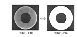
- FIG. 6 shows a state of surface light emission in the ring cover 4.
- the left side shows a state where the diffusion beads BS are not provided
- the right side shows a state where the diffusion beads BS are provided as in this embodiment.
- the uneven luminance of surface emission is conspicuous, but when the diffusion beads BS are provided, the uneven luminance of surface emission is suppressed.
- the method of providing the diffusing beads BS as in the present embodiment is adopted in changing the specifications of the illumination lamp A, it is advantageous from various viewpoints because uneven luminance of surface emission is suppressed.
- the number of LEDs 32a may be reduced in order to reduce the manufacturing cost.
- the spatial distance from the LED 32a to the ring cover 4 may be shortened.
- this is simply done, it is assumed that the luminance unevenness of the surface emission increases and exceeds the allowable range.
- the number of LEDs 32a in the illumination lamp A can be reduced while the luminance unevenness does not deviate from the allowable range compared to the case where the diffusion beads BS are not provided. It is easy to reduce the thickness.
- a sheet material that is the base of the ring cover 4 is generated.
- a mixed resin in which the diffusion beads BS are kneaded (mixed) into the resin is used.
- a sheet material is generated from the mixed resin by extrusion molding using a predetermined extrusion molding machine.
- the molding conditions, the state of the mixed resin, and the like are appropriately adjusted in advance so that a part of the diffusion beads BS protrudes from the surface of the sheet material.
- the resin for example, an acrylic resin such as PMMA, polystyrene, or polycarbonate, which is a light resin having a high transmittance and a milky white color, is used.
- the diffusion beads BS for example, particles of an inorganic material that easily scatters light are used.
- the average particle diameter of the diffusion beads BS is within an appropriate range of 20 to 60 ⁇ m.
- the sheet material 41 described above is placed between the upper heater 91a and the lower heater 91b, and the sheet material 41 is warmed and softened. Thereafter, as shown in FIG. 7 (2), the sheet material 41 is fixed on the molding apparatus, and the sheet material 41 is expanded by sending air from below. Thereafter, as shown in FIG. 7 (3), the die 92 corresponding to the shape of the ring cover 4 is lifted and set in the space portion generated by the swelling of the sheet material 41.
- the sheet material 41 is brought into close contact with the mold 92 by sucking air from the lower side.
- the sheet material 41 is brought into close contact with the mold 92 by air pressure from the outside, and air is sucked from below. It is also possible to use a vacuum / compressed air combination molding method. After the series of steps described above, the ring cover 4 is completed by further cooling and necessary processing.
- the ring cover 4 generated in this way is in a state where the diffusion beads BS are provided so as to protrude from the surface (particularly the light receiving surface). Therefore, as described above, it is used as a component of the illumination lamp A and exhibits the effect of suppressing unevenness in luminance of surface light emission.
- the ring cover 4 contains inorganic particles or organic particles such as diffusion beads BS and pigments.
- generating a sheet material from the mixed resin mentioned above and molding this sheet material is the cover 60 of 3rd Example, or the optical sheet member 822 of 4th Example (all are , which will be described later in detail).
- the second embodiment is basically the same as the first embodiment except that a direct light source is mainly used.
- emphasis is placed on the description of points that are different from the first embodiment, and descriptions of points that are common to the first embodiment may be omitted.
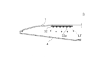
- FIG. 8 shows a partial cross-sectional view (a view from the same viewpoint as FIG. 5) of the illuminating lamp B according to the second embodiment when cut along a plane including the central axis X.
- an LED substrate 32 on which LEDs 32a are mounted is attached to the lower side surface of the chassis 1 (the surface facing the light receiving surface (upper side surface) of the ring cover 4).
- the LED 32a is provided so as to irradiate light downward as indicated by broken line arrows in FIG. Therefore, the light of the LED 32 a is irradiated almost directly toward the light receiving surface of the ring cover 4. Thereby, as for the ring cover 4, the light emission surface (lower side surface) will carry out surface light emission.
- the point that the LED 32a emits light using the power supplied from the drive control unit is the same as in the first embodiment.
- the illumination lamp B may be provided with a lens through which light from the light source passes, as in the first embodiment.
- the illuminating lamp B is a ceiling light (directly-type ceiling light) that illuminates using the light of the LED 32a, which is a direct light source.
- the ring cover 4 is provided with the diffusion beads BS so as to protrude from the light receiving surface, so that uneven luminance of surface light emission can be suppressed. ing.
- FIG. 9 shows a state of surface light emission in the ring cover 4 of the second embodiment.
- the left side shows the state when the diffusion beads BS are not provided
- the right side shows the state when the diffusion beads BS are provided as in this embodiment.
- the luminance unevenness is noticeable when the diffusion beads BS are not provided, but the luminance unevenness is suppressed when the diffusion beads BS are provided.
- a ceiling light of a type that is attached to the ceiling is mentioned as an example of the illumination lamp.
- the illuminating lamp using the illuminating device of the present invention is not limited to a ceiling light, and may be a hanging type illuminating lamp, for example.
- the chassis 1 according to each of the above-described embodiments has a substantially disk shape, for example, a polygonal shape may be used as the chassis.
- a light emitting unit including a light source may be disposed on the edge of the chassis so as to be suitable for this shape.
- an explanation will be given by taking as an example an illuminating lamp in which a substantially rectangular parallelepiped chassis is used and a light emitting portion is arranged on the edge of the chassis.
- a substantially rectangular parallelepiped chassis is used and a light emitting portion is arranged on the edge of the chassis.
- emphasis is placed on the description of parts different from the first embodiment, and description of common parts may be omitted.
- FIG. 10 shows an exploded perspective view of the illuminating lamp C according to the third embodiment.
- the illuminating lamp C includes a chassis 6 and a cover 60 that covers the chassis 6.
- the chassis 6 is formed by cutting and bending a metal plate, and includes a rectangular flat plate portion 61 and side wall portions 62 formed by bending each side of the flat plate portion.
- the cover 60 is formed in a substantially plate shape.
- the chassis 6 is a casing having a shape in which one surface of a rectangular parallelepiped is opened, and the cover 60 is attached and fixed to the side wall portion 62 so as to cover the opening.
- the LED board 32 in which LED32a was mounted is attached along with the side wall part 62 formed by bending the short side of the flat plate part 61 of the chassis 6. As shown in FIG.
- the flat plate portion 61 of the chassis 6 is configured to efficiently reflect the light of the LED 32a toward the cover 60 side. Examples of the treatment of the flat plate portion 61 include well-known ones such as white coating and reflection sheet pasting. Further, the illumination lamp C may be provided with a lens through which light from the light source passes, as in the first embodiment.
- the light emitted from the LED 32a directly hits the light receiving surface (upper surface in FIG. 10) of the cover 60 as direct light, or as reflected light reflected by the surface of the chassis 6 (reflecting surface). , It hits the light receiving surface of the cover 60.
- the light emitting surface (the lower surface in FIG. 10) emits light.
- the illumination lamp C illuminates the outside.
- the parts corresponding to the drive control unit 2 in the first embodiment are not shown, but are attached to the back surface of the flat plate portion 61.
- components corresponding to the drive control unit 2 and the LED angle 31 are disposed at positions that do not obstruct the light path of the LED 32a as much as possible. For this reason, it is possible to reduce or eliminate the non-light-emitting portion, and it is possible to reduce unevenness in luminance of surface light emission in the cover 60.
- the cover 60 has a shape different from that of the ring cover 4 of the first embodiment, the raw material, the production method, and the like are in accordance with the specifications of the ring cover 4. Accordingly, the cover 60 is provided with the diffusion beads BS so as to protrude from the surface (particularly, the light receiving surface), and scatters the light of the LED 32a in various directions. Therefore, according to the illuminating lamp C, luminance unevenness can be suppressed by the same principle as in the first embodiment.
- the through-hole is formed in the center part (it shows with a broken line in FIG. 10) of the flat plate part 61, and the connector arrange
- FIG. 11 is an exploded perspective view of the liquid crystal display device 8 according to the fourth embodiment.
- the liquid crystal display device 8 includes a liquid crystal panel unit 81 and a backlight unit 82.
- a liquid crystal panel unit 81 is disposed on the front side (observer side) of the backlight unit 82, and the front side of the liquid crystal panel unit 81 is pressed by a metal bezel 83.
- the liquid crystal panel unit 81 includes a liquid crystal panel 811 in which liquid crystal is sealed, and a polarizing plate 812 attached to the front surface (observer side) and the back surface (backlight unit 82 side) of the liquid crystal panel 811.
- the liquid crystal panel 811 includes an array substrate 813, a counter substrate 814 disposed to face the array substrate 813, and liquid crystal filled between the array substrate 813 and the counter substrate 814.
- the array substrate 813 is provided with a source wiring and a gate wiring orthogonal to each other, a switching element (for example, a thin film transistor) connected to the source wiring and the gate wiring, a pixel electrode connected to the switching element, an alignment film, and the like.
- the counter substrate 814 is provided with a color filter in which colored portions of red, green, and blue (RGB) are arranged in a predetermined arrangement, a common electrode, an alignment film, and the like.
- a voltage is applied between the array substrate 813 and the counter substrate 814 in each pixel of the liquid crystal panel 811 by driving the switching element.
- the voltage between the array substrate 813 and the counter substrate 814 changes, the liquid crystal in each pixel rotates and light is modulated (the degree of light transmission is changed). As a result, an image is displayed in the image display area on the viewer side of the liquid crystal panel 811.
- the bezel 83 is a metal frame, and has a shape that covers the front edge portion of the liquid crystal panel unit 81.
- the bezel 83 includes a rectangular opening window 830 formed so that the image display area of the liquid crystal panel unit 81 is not hidden, a pressing portion 831 for pressing the liquid crystal panel unit 81 from the front side, and a rear side from the edge of the pressing portion 831. And a cover portion 832 that covers the edges of the liquid crystal panel unit 81 and the backlight unit 82.
- the bezel 83 is grounded and shields the liquid crystal panel unit 81 and the backlight unit 82.
- the backlight unit 82 is an illumination device that irradiates the liquid crystal panel unit 81 with planar light.
- the backlight unit 82 has a structure equivalent to or equivalent to the illumination lamp A according to the first embodiment. More specifically, a backlight chassis 821 having a rectangular bottom surface corresponding to the chassis 1 of the first embodiment, an optical sheet member 822 corresponding to the ring cover 4 of the first embodiment, and the LED substrate 32 are provided. Have.
- the backlight unit 82 is a member having a rectangular bottom surface, and the LED substrate 32 is disposed on both short sides. Although not shown, components corresponding to the drive control unit 2 of the first embodiment are mounted and arranged on the back side (lower side in FIG. 11) of the backlight chassis 821. An optical sheet member 822 is disposed on the light emission surface side (the upper side in FIG. 11) of the backlight unit 82.
- the LED board 32 is mounted with LEDs 32a, and a plurality of LED boards 32 are attached to each short side of the backlight chassis 821.
- a backlight unit 82 it is possible to emit planar light with less luminance unevenness than the light emitting surface facing the bottom without using a light guide plate.
- the backlight unit 82 According to the backlight unit 82, the light emitted from the LED 32a directly hits the light receiving surface (the lower surface in FIG. 11) of the optical sheet member 822 as direct light, and also the surface (reflecting surface) of the backlight chassis 821. The reflected light that hits the light hits the light receiving surface of the optical sheet member 822. In the optical sheet member 822, when the light of the LED 32a hits the light receiving surface, the light emitting surface (the upper surface in FIG. 11) emits light. As a result, the backlight unit 82 illuminates the liquid crystal panel unit 81 from the back side (that is, supplies light from the backlight).
- the optical sheet member 822 is different in shape from the ring cover 4 of the first embodiment, but the raw material, the production method, and the like are based on the specifications of the ring cover 4. Thereby, the optical sheet member 822 is provided with the diffusion beads BS so as to protrude from the surface (particularly, the light receiving surface), and scatters the light of the LED 32a in various directions. Therefore, according to the backlight 8, the luminance unevenness of the surface emission is suppressed by the same principle as in the first embodiment.
- the liquid crystal display device shown in this embodiment can be employed in, for example, a mobile phone, a tablet PC, a display device for household electric appliances, a television receiver, and the like.
- the illuminating device has a light source and a substantially plate-like plate-like portion.
- the light-receiving surface which is one surface of the plate-like portion, receives light
- the light emitting surface which is a surface, includes an optical member that emits light, and the light emitting surface is illuminated by applying light emitted from a light source to the light receiving surface.
- the ring cover 4 corresponds to the optical member
- the cover 60 corresponds to the optical member
- the optical sheet member 822 corresponds to the optical member.
- the plate-like portion is provided with diffusion beads BS that scatter light emitted from the light source so as to protrude from the light receiving surface. Therefore, the illuminating device according to each embodiment can suppress uneven luminance of surface light emission while illuminating using surface light emission of the optical member.
- the illuminating device of each Example is used for the backlight of an illuminating lamp or a liquid crystal display device, the use of the illuminating device of this invention is not restricted to these.
- the illuminating device of the present invention can be used in various applications in which illumination is used, such as a back-side illuminating device that illuminates from the back of an electric signboard or the like.
- the light source in the illumination device of the present invention is not limited to the LED, and other types of light sources can be applied.
- the configuration of the present invention can be variously modified in addition to the above-described embodiments without departing from the gist of the invention. That is, the above-described embodiment is an example in all respects and should not be considered as limiting, and the technical scope of the present invention is not the description of the above-described embodiment, but the claims. It should be understood that all modifications that come within the meaning and range of equivalents of the claims are included.
- the present invention can be used for illumination lamps and backlights.
Landscapes
- Physics & Mathematics (AREA)
- General Physics & Mathematics (AREA)
- Optics & Photonics (AREA)
- Chemical & Material Sciences (AREA)
- Dispersion Chemistry (AREA)
- Planar Illumination Modules (AREA)
Abstract
光源と、略板状の板状部を有し、該板状部の一方の面である受光面に光を受けて、他方の面である発光面が面発光する光学部材と、を備え、前記受光面に前記光源から照射された光を当てることにより、前記発光面を面発光させて照明する照明装置であって、前記板状部には、前記光源から照射された光を散乱させる拡散ビーズが、前記受光面から突出するように設けられている照明装置とする。
Description
本発明は、光学部材の面発光を利用して照明する照明装置、ならびに、この照明装置を利用した照明灯、バックライト、液晶表示装置、およびテレビジョン受信装置に関するものである。
従来、光学部材の面発光を利用して照明する照明装置が提案されている(例えば特許文献1を参照)。このような照明装置は、光学部材が光源の光を受けて面発光するように形成されており、照明灯などに利用される。
またこのような照明装置において、光源としては、例えば発光ダイオード(LED)が用いられる。LEDは、従来用いられてきた蛍光ランプ(冷陰極管等)に比べ、それ自体小型で長寿命、高い発光効率による低消費電力、水銀を使わない等の多くの優れた点を有している。
上述した照明装置においては、適切な照明を得るべく、面発光の輝度は出来るだけ均一であることが望ましい。しかしながら、例えば、LED等の光源の密度が不足していたり、光源から光学部材までの空間距離が不足していたりすると、光源の光が十分に拡散せず、光学部材の面発光における輝度のムラ(輝度ムラ)が多くなり易い。
また上述した照明装置の仕様について、例えば、製造コストが重視される場合には、LEDの個数削減等により、光源の密度が比較的小さくされ易い。また例えば、薄型化が重視される場合には、光源から光学部材までの空間距離が比較的小さくされ易い。
しかしこのように、光源の密度や当該空間距離が削減されると、面発光の輝度ムラの増大が大きな問題となる。また光源の密度や当該空間距離を増大させずに、面発光の輝度ムラを低減させたい場合もある。
本発明は上述した問題に鑑み、光学部材の面発光を利用して照明するものであって、面発光の輝度ムラを抑えることが可能となる照明装置の提供を目的とする。また本発明は、このような照明装置を利用した照明灯、バックライト、液晶表示装置、およびテレビジョン受信装置の提供を更なる目的とする。
上記目的を達成するため本発明に係る照明装置は、光源と、略板状の板状部を有し、該板状部の一方の面である受光面に光を受けて、他方の面である発光面が面発光する光学部材と、を備え、前記受光面に前記光源から照射された光を当てることにより、前記発光面を面発光させて照明する照明装置であって、前記板状部には、前記光源から照射された光を散乱させる拡散ビーズが、前記受光面から突出するように設けられている構成とする。
本構成によれば、光学部材の面発光を利用して照明するものでありながら、面発光の輝度ムラを抑えることが可能となる。
また上記構成としてより具体的には、前記光学部材は、樹脂に前記拡散ビーズを混ぜ合わせた混合樹脂を原料として、生成されている構成としてもよい。また上記構成としてより具体的には、前記光学部材は、前記混合樹脂により形成された板状体の成形によって、生成されている構成としてもよい。
また上記構成としてより具体的には、前記光源はLEDである構成としてもよい。また上記構成としてより具体的には、前記拡散ビーズは平均粒径が20~60μmである構成としてもよい。
また上記構成としてより具体的には、光を反射させる反射面を有した構成部材を備えており、前記光源の光が前記受光面と前記反射面に挟まれた空間に向けて光を照射されることにより、直接光および前記反射面で反射した反射光が前記受光面に当たるようにした構成としてもよい。
また上記構成としてより具体的には、全体形状が略円盤形状に形成されており、前記光源は、前記受光面と前記反射面に挟まれた空間よりも、前記円盤形状の中心軸に近い位置に配置されている構成としてもよい。
また本発明に係る照明灯は、上記構成に係る照明装置が用いられた構成とする。本構成によれば、上記構成に係る照明装置の利点が得られる。また当該照明灯は、例えば、シーリングライトとしてもよい。
また本発明に係るバックライトは、上記構成に係る照明装置が用いられた構成とする。そして本発明に係る液晶表示装置は、当該バックライトを備えた構成とする。また更に本発明に係るテレビジョン受信装置は、当該液晶表示装置を備えた構成とする。これらの構成によれば、上記構成に係る照明装置の利点が得られる。
本発明の照明装置によれば、光学部材の面発光を利用して照明するものでありながら、面発光の輝度ムラを抑えることが可能となる。また本発明の照明灯、バックライト、液晶表示装置、或いはテレビジョン受信装置によれば、本発明の照明装置の利点を得ることが可能となる。
本発明の実施形態について、第1から第4の各実施例を挙げて以下に説明する。なお、第1から第3実施例では、本発明の照明装置が照明灯に用いられた例を挙げ、第4実施例では、本発明の照明装置が液晶表示装置用のバックライト(バックライトユニット)に用いられた例を挙げている。
1.第1実施例
[照明灯の構成および基本動作等]
まず第1実施例に係る照明灯Aの構成について、図1から図3の各図を参照しながら説明する。図1は照明灯A(中心軸Xを含む面で切断した状態)の斜視図であり、図2は図1に示す枠FRの部分の拡大図である。なお照明灯Aは、全体形状が略円盤形状となっており、中心軸Xはこの円盤形状の中心軸(対称軸)に相当する。また図3は、照明灯Aの分解斜視図である。なお図3における一点鎖線で囲まれた部分は、LED基板32のより詳細な構成を表している。
[照明灯の構成および基本動作等]
まず第1実施例に係る照明灯Aの構成について、図1から図3の各図を参照しながら説明する。図1は照明灯A(中心軸Xを含む面で切断した状態)の斜視図であり、図2は図1に示す枠FRの部分の拡大図である。なお照明灯Aは、全体形状が略円盤形状となっており、中心軸Xはこの円盤形状の中心軸(対称軸)に相当する。また図3は、照明灯Aの分解斜視図である。なお図3における一点鎖線で囲まれた部分は、LED基板32のより詳細な構成を表している。
照明灯Aは、天井面に取り付けられるシーリングライトであり、上部が天井面に取り付けられる。なお、以下の説明における上下の方向は、別途記載した場合を除き、図1における上下の方向(中心軸の方向)を意味する。また、中心軸Xから垂直に外側へ向かう方向をH方向(ホリゾンタル方向)として説明する場合もある。
図3に示すように照明灯Aは、シャーシ1、駆動制御部2、発光部3、リングカバー4、PWBカバー51、およびセンターカバー52を備えており、上からこの順番で配置されている。シャーシ1は、天井面に取り付けられる筐体であり、アルミニウムで形成された略円板状の部材である。シャーシ1の中央部分には、天井面に備えられた電力供給用の電源コネクタ(不図示)が貫通する。
シャーシ1の下側の面は、発光部3から出射された光を効率よく反射する反射面として形成されており、表面処理がなされている。なお、この表面処理としては、例えば、発泡PET等の反射率の高いシートを貼り付ける方法や、白色の塗料を塗布するものが採用されていてもよい。
駆動制御部2は、発光部3に電力を供給する電源回路や、点灯制御を行う制御回路等の回路を含む。駆動制御部2は、シャーシ1への漏電を抑制するための絶縁シート20と、電源回路や制御回路等が実装された電源基板21と、電源基板21を上側から支持するPWB支持板22と、電源基板21を下側から支持するPWB支持板23を備えている。駆動制御部2は、天井面に備えられた電源コネクタ(不図示)と電気的に接続され、供給された電力を発光部3に対応した電力に変換する回路も備えている。
発光部3は、LEDアングル31と、光源であるLED32aが実装されたLED基板32と、レンズ(例えばコリメータレンズ)を有するレンズ部材33を備えている。
LEDアングル31は、LED基板32やレンズ部材33が取り付けられるとともに、ねじ止めによってシャーシ1に固定される。これによりLEDアングル31は、LED基板32やレンズ部材33を、シャーシ1に固定させる役割を果たす。またLEDアングル31は、ねじ止め等により、駆動制御部2やリングカバー4にも固定される。
LED基板32は、外縁が略長方形に形成されており、複数個のチップ状のLED32aが実装されている。LED32aは、駆動制御部2から供給される電力を用いて発光する。レンズ部材33は、LED基板32をH方向外側から覆うように配置されており、LED32aから出射される光がレンズを通るようにする。
リングカバー4は、略円板形状に形成されている部材であり、下側からシャーシ1に取り付けられている。リングカバー4は、外周部分がシャーシ1に係合されるとともに、中央部分が発光部3にねじ止めされることで固定されている。なお詳しくは後述するが、リングカバー4は、上側面(受光面)にLED32aの光を受けたときに下側面(発光面)が面発光する、光学部材として形成されている。照明灯Aは、リングカバー4の受光面にLED32aから照射された光を当てることにより、リングカバー4の発光面を面発光させて外部を照明する。
なおリングカバー4は、LED32aから照射された光を散乱させる拡散ビーズを含有し、かつ、当該拡散ビーズが受光面から突出するように設けられている。拡散ビーズを設ける理由やリングカバー4の生成工程については、改めて詳細に説明する。
また照明灯Aの下側中央部には、電源基板21を保護するPWBカバー51が取り付けられている。また更にその下側には、照明灯Aの下側中央部を覆うように、センターカバー52が取り付けられている。
次に、発光部3の構成についてより詳細に説明する。図4は、発光部3の下方視点による構成図である。本図に示すようにLEDアングル31は、隣り合うもの同士がつなぎ合わさって、中心軸Xを中心とする正八角形断面の筒形状を形成している。またLED基板32およびレンズ部材33は、LED32aの光が概ねH方向へ照射されるように配列された状態で、各LEDアングル31にねじ止めされている。これによりLED32aの光LTは、図4の破線矢印で示すように、概ねH方向へ満遍なく広がるように照射される。
また図5は、中心軸Xを含む面で切断した場合の照明灯Aの一部の断面図である。なお本図において、左下の部分には、実線で囲まれた部分の拡大図(一の拡散ビーズBSにLED32aの光が入射した状態を、模式的に示した図)が示されている。
図5に破線矢印で示すように、LED32aの光LTは、シャーシ1とリングカバー4の間に形成された空間に向けて照射されることになる。これによりLED32aの光LTは、直接光としてリングカバー4の受光面SF1に直接当たる他、シャーシ1(光を反射させる反射面を有した構成部材)に当たって反射した反射光として、リングカバー4の受光面SF1に当たることになる。
このように照明装置Aでは、LED32aの光LTが受光面SF1とシャーシ1の反射面に挟まれた空間に向けて照射されることにより、直接光および当該反射面で反射した反射光が受光面SF1に当たるようになっている。またリングカバー4は、受光面SF1にLED32aの光LTが当たると、発光面SF2が面発光する。なおLED32aは、受光面SF1と当該反射面に挟まれた空間より、中心軸Xに近い位置に配置されていると言える。
ここで図5の左下の部分に示すように、リングカバー4には、LED32aの光LTを散乱させる拡散ビーズBSが、受光面SF1から突出するように設けられている。この突出した拡散ビーズBSにLED32aの光LTが入射すると、光LTは実線矢印で示すように散乱反射したり透過したりし、また更には多重反射することもあり、様々な方向へ散乱することとなる。
[拡散ビーズを設けることによる効果]
上述したようにリングカバー4は、受光面から突出するように拡散ビーズBSが設けられており、LED32aの光LTを様々な方向へ散乱させるようになっている。そのため照明灯Aによれば、面発光の輝度ムラが抑えられるようになっている。
上述したようにリングカバー4は、受光面から突出するように拡散ビーズBSが設けられており、LED32aの光LTを様々な方向へ散乱させるようになっている。そのため照明灯Aによれば、面発光の輝度ムラが抑えられるようになっている。
例えば、LED32aの個数が比較的少ない場合(光源の密度が小さい場合)、或いは、LED32aからリングカバー4までの空間距離が比較的短い場合には、照明灯A内においてLED32aの光LTを十分に拡散させることが難しく、面発光の輝度ムラが生じ易い。しかし本実施例のように拡散ビーズBSが設けられていれば、拡散ビーズBSがLED32aの光LTを散乱させることによって光LTの拡散が促進され、面発光の輝度ムラが抑えられることになる。
図6は、リングカバー4における面発光の様子を表している。なお図6において、左側は拡散ビーズBSを設けない場合の様子を、右側は本実施例のように拡散ビーズBSを設けた場合の様子を、それぞれ表している。本図に示すように、拡散ビーズBSを設けない場合には面発光の輝度ムラが目立っているが、拡散ビーズBSを設けた場合には面発光の輝度ムラが抑えられている。
なお照明灯Aの仕様変更等において、本実施例のように拡散ビーズBSを設ける手法を採用する場合には、面発光の輝度ムラが抑えられるため、種々の観点から有利となる。例えば、製造コストの削減を図るため、LED32aの個数削減が行われる場合があり得る。また薄型化を図るため、LED32aからリングカバー4までの空間距離が短くされる場合があり得る。しかし単にこのようにすると、面発光の輝度ムラが増長され、許容範囲を超えてしまうことが想定される。
この点、本実施例のように拡散ビーズBSを設けるようにすれば、拡散ビーズBSを設けない場合に比べ、輝度ムラが許容範囲を逸脱しないようにしつつ、照明灯AにおけるLED32aの個数削減や薄型化を図ることが容易となる。
また現状よりも輝度ムラの低減を目指す場合、LED32aの増設や、LED32aからリングカバー4までの空間距離を長くすることも考えられるが、製造コストの増大や薄型化の阻害が問題となる。この点、本実施例のように拡散ビーズBSを設けるようにすれば、このような問題を殆ど生じさせずに、輝度ムラの低減が達成される。
[リングカバーの生成工程]
次に、リングカバー4の生成工程の一例について、図7を参照しながら説明する。ここでは、成形用の型(縦型)を用いてシート材(板状体)を成形することにより、リングカバー4を生成する例を挙げる。
次に、リングカバー4の生成工程の一例について、図7を参照しながら説明する。ここでは、成形用の型(縦型)を用いてシート材(板状体)を成形することにより、リングカバー4を生成する例を挙げる。
まずリングカバー4の元となるシート材が生成される。シート材の原料としては、樹脂に拡散ビーズBSを練り込んだ(混ぜ合わせた)混合樹脂が用いられる。そして所定の押出し成形機を用いた押出し成形により、この混合樹脂からシート材が生成される。なお、この際の成形条件や混合樹脂の状態等は、拡散ビーズBSの一部がシート材の表面から突出するように、予め適切に調整されている。
またここでの樹脂としては、例えば、PMMAなどのアクリル樹脂、ポリスチレン、或いはポリカーボネイトといった透過率が高くて軽量な樹脂であって、乳白色のものが用いられる。また拡散ビーズBSとしては、例えば、光を散乱させ易い無機系材質の粒子が用いられる。
なお、拡散ビーズBSの粒径が小さ過ぎる場合には、拡散ビーズ4がリングカバー4から突出することによるリングカバー4の受光面の粗さが足りなくなり、十分な輝度ムラの改善効果を得ることが難しくなる。一方、大き過ぎる場合には、リングカバー4の表面に視覚的な粗さ(ザラザラ感)が出るため、リングカバー4の外観に不具合が生じ易くなる。主にこのような観点から、拡散ビーズBSの平均粒径は、20~60μmの適切な範囲内であることが望ましい。
そして図7(1)に示すように、上側ヒータ91aと下側ヒータ91bの間に上述したシート材41を置き、シート材41を温めて柔らかくする。その後、図7(2)に示すように、シート材41を成形装置の上に固定し、下側から空気を送り込むことによってシート材41を膨らませる。さらにその後、図7(3)に示すように、リングカバー4の形状に対応した型92を持ち上げ、シート材41の膨らみによって生じた空間部分にセットする。
その後、真空成形の場合には、図7(4)に示すように、下側から空気を吸引することによって、シート材41を型92に密着させる。なお圧空成形の場合には、図7(4´)に示すように、外側からの空気圧によってシート材41を型92に密着させるとともに、下側から空気を吸引する。なお、真空/圧空併用型の成形手法を用いることも可能である。上述した一連の工程を経た後、更に冷却や必要な加工処理等が施され、リングカバー4が完成する。
このようにして生成されたリングカバー4は、表面(特に受光面)から突出するように拡散ビーズBSが設けられた状態となっている。そのため、先述したように照明灯Aの部品として用いられて、面発光の輝度ムラを抑える効果を発揮する。なおリングカバー4の内部には、拡散ビーズBSや顔料など、無機系材質の粒子や有機系材質の粒子が混入している。
ところで、リングカバー4の表面に粗さを付けるにあたっては、予めシボ加工を施したシート材を用いてリングカバー4を生成することも有効であるように見える。しかしこの場合は、図7(2)に示すようにシート材を膨らませる過程において、シボ加工の施された部分が延ばされてしまい、シボ加工による粗さが減少する。この点、本実施例のように、拡散ビーズBSを用いていれば、シート材を膨らませても表面の粗さが殆ど減少せず、リングカバー4に十分な散乱面が残るため、輝度ムラをより効果的に抑制できるものとなる。
なお、上述した混合樹脂からシート材を生成しておき、このシート材を成形することによって部品を生成する手法は、第3実施例のカバー60や第4実施例の光学シート部材822(何れも、詳しくは後述する)の生成にも適用可能である。
2.第2実施例
次に、第2実施例について説明する。なお第2実施例は、主に直下型の光源を採用した点を除いて、基本的には第1実施例と同等である。以下の説明では、第1実施例と異なる点の説明に重点を置き、第1実施例と共通の点については説明を省略することがある。
次に、第2実施例について説明する。なお第2実施例は、主に直下型の光源を採用した点を除いて、基本的には第1実施例と同等である。以下の説明では、第1実施例と異なる点の説明に重点を置き、第1実施例と共通の点については説明を省略することがある。
図8は、中心軸Xを含む面で切断した場合における、第2実施例に係る照明灯Bの一部の断面図(図5と同様の視点による図)を示している。本図に示すように照明灯Bでは、シャーシ1の下側面(リングカバー4の受光面(上側面)と向かい合う面)に、LED32aを実装したLED基板32が取り付けられている。
なおLED32aは、図8に破線矢印で示す通り下方に向けて光を照射するように、設けられている。そのためLED32aの光は、リングカバー4の受光面に向けて概ね直下的に照射される。これによりリングカバー4は、発光面(下側面)が面発光することとなる。なおLED32aが、駆動制御部からの供給電力を用いて発光する点などは、第1実施例の場合と同様である。また照明灯Bには、第1実施例の場合と同様に、光源の光が通るようにしたレンズが設けられていても良い。
このように照明灯Bは、直下型光源であるLED32aの光を用いて照明するシーリングライト(直下型のシーリングライト)となっている。また照明灯Bにおいても、第1実施例の場合と同様に、リングカバー4には受光面から突出するように拡散ビーズBSが設けられているため、面発光の輝度ムラが抑えられるようになっている。
図9は、第2実施例のリングカバー4における面発光の様子を表している。なお図9において、左側は拡散ビーズBSを設けない場合の様子を、右側は本実施例のように拡散ビーズBSを設けた場合の様子を、それぞれ表している。本図に示すように、拡散ビーズBSを設けない場合には輝度ムラが目立っているが、拡散ビーズBSを設けた場合には輝度ムラが抑えられている。
なお上述の各実施例では、照明灯の例として、天井に取り付けるタイプのシーリングライトを挙げた。但し、本発明の照明装置を用いる照明灯はシーリングライトに限られることなく、例えば、吊り下げ型の照明灯などとすることも可能である。
3.第3実施例
次に、第3実施例について説明する。上述の各実施例に係るシャーシ1は略円板形状であるが、シャーシとしては、例えば多角形の形状のものが用いられることもあり得る。またこの形状に適するように、光源を含む発光部がシャーシの辺縁部に配置されることがあり得る。
次に、第3実施例について説明する。上述の各実施例に係るシャーシ1は略円板形状であるが、シャーシとしては、例えば多角形の形状のものが用いられることもあり得る。またこの形状に適するように、光源を含む発光部がシャーシの辺縁部に配置されることがあり得る。
ここでは第3実施例として、略直方体のシャーシが用いられ、更にシャーシの辺縁部に発光部を配置した照明灯を例に挙げて説明する。なお以下の説明においては、第1実施例と異なる部分の説明に重点を置き、共通する部分については説明を省略することがある。
図10は、第3実施例に係る照明灯Cの分解斜視図を示す。本図に示すように照明灯Cは、シャーシ6と、シャーシ6を覆うカバー60とを備えている。シャーシ6は金属板を切り曲げて形成されており、長方形の平板部61と、平板部の各辺を折り曲げて形成した側壁部62とを備えている。またカバー60は、略板状に形成されている。
つまりシャーシ6は、直方体の一つの面が開口した形状の筐体となっており、カバー60は、この開口を覆うように側壁部62に取り付け固定されている。そして、図10に示すように、シャーシ6の平板部61の短辺を折り曲げて形成した側壁部62に、LED32aが実装されたLED基板32が並んで取り付けられている。
このように照明灯Cでは、側壁部62の一部が、第1実施例におけるLEDアングル31に準じた役割を果たしている。そのため、LEDアングル31に相当する部品が省略可能となっている。また、シャーシ6の平板部61は、LED32aの光をカバー60側に効率よく反射することができる構成となっている。平板部61の処理としては、白色の塗装、反射シートの貼り付け等、従来よく知られているものが挙げられる。また照明灯Cには、第1実施例の場合と同様に、光源の光が通るようにしたレンズが設けられていても良い。
照明灯Cによれば、LED32aから照射された光は、直接光としてカバー60の受光面(図10における上側の面)に直接当たる他、シャーシ6の表面(反射面)に当たって反射した反射光として、カバー60の受光面に当たることになる。カバー60は、受光面にLED32aの光LTが当たると、発光面(図10における下側の面)が面発光する。これにより、照明灯Cは外部を照明することになる。
また第1実施例における駆動制御部2に相当する部品は、図示を省略しているが、平板部61の裏面に取り付けられている。このような構成の照明灯Cでは、駆動制御部2やLEDアングル31に相当する部品が、LED32aの光の進路を極力妨げない位置に配置されている。そのため、無発光部分を低減あるいはなくすことが可能であり、カバー60における面発光の輝度ムラを低減させることが可能である。
また更にカバー60は、第1実施例のリングカバー4とは形状が異なるものの、原料や生成方法などはリングカバー4に準じた仕様となっている。これによりカバー60は、表面(特に受光面)から突出するように拡散ビーズBSが設けられており、LED32aの光を様々な方向へ散乱させるようになっている。そのため照明灯Cによれば、第1実施例の場合と同様の原理により、輝度ムラが抑えられるようになっている。
なお照明灯Cを天井に取り付ける仕様とする場合は、例えば、平板部61の中央部(図10に破線で示す)に貫通孔を形成しておき、天井に配置されたコネクタをこの貫通孔に通すことによって、照明灯Cを当該コネクタに固定できるようにしてもよい。
4.第4実施例
本発明の照明装置は面発光により面状光を出射するものであることから、液晶表示装置のバックライトとしても利用可能である。ここでは、本発明の照明装置を液晶表示装置のバックライトとして利用する形態の一例を、第4実施例として説明する。図11は、第4実施例に係る液晶表示装置8の分解斜視図である。
本発明の照明装置は面発光により面状光を出射するものであることから、液晶表示装置のバックライトとしても利用可能である。ここでは、本発明の照明装置を液晶表示装置のバックライトとして利用する形態の一例を、第4実施例として説明する。図11は、第4実施例に係る液晶表示装置8の分解斜視図である。
図11に示すように、液晶表示装置8は、液晶パネルユニット81と、バックライトユニット82とを備えている。液晶表示装置8においては、バックライトユニット82の前面側(観察者側)に液晶パネルユニット81が配置され、液晶パネルユニット81の前面側は、金属製のベゼル83に押えられている。
液晶パネルユニット81は、液晶が封入された液晶パネル811と、液晶パネル811の前面(観察者側)及び背面(バックライトユニット82側)に貼り付けられた偏光板812とを有している。液晶パネル811は、アレイ基板813と、アレイ基板813に対向して配置された対向基板814と、アレイ基板813と対向基板814の間に充填される液晶とを含んでいる。
アレイ基板813には、互いに直交するソース配線及びゲート配線、ソース配線及びゲート配線に接続されたスイッチング素子(例えば、薄膜トランジスタ)、スイッチング素子に接続された画素電極及び配向膜等が設けられている。そして、対向基板814には、赤、緑、青(RGB)の各着色部が所定の配列で配置されたカラーフィルタ、共通電極、配向膜等が設けられている。
液晶パネルユニット81においては、スイッチング素子が駆動されることで、液晶パネル811の各画素におけるアレイ基板813と対向基板814との間に電圧が印加される。アレイ基板813と対向基板814の間の電圧が変化することで、各画素での液晶が回転し、光が変調される(光の透過度合いが変更される)。これにより、液晶パネル811の観察者側の画像表示領域に画像を表示する。
ベゼル83は、金属製の枠体であり、液晶パネルユニット81の前面の辺縁部分を覆う形状を有している。ベゼル83は、液晶パネルユニット81の映像表示領域が隠れないように形成された矩形の開口窓830と、液晶パネルユニット81を前面側から押える押え部831と、押え部831の辺縁部より背面側に突出し、液晶パネルユニット81及びバックライトユニット82の辺縁部を覆うカバー部832と、を備えている。ベゼル83は接地されており、液晶パネルユニット81及びバックライトユニット82をシールドしている。
バックライトユニット82は、液晶パネルユニット81に面状光を照射する照明装置である。バックライトユニット82は、原理的には、第1実施例に係る照明灯Aと同等或いはこれに準じた構造を有している。より具体的には、第1実施例のシャーシ1に相当する長方形状の底面を有するバックライトシャーシ821と、第1実施例のリングカバー4に相当する光学シート部材822と、LED基板32とを有している。
なお、バックライトユニット82は、長方形状の底面を有する部材であることに鑑み、短辺の両方にLED基板32が配置されている。そして図示は省略しているが、第1実施例の駆動制御部2に相当する部品は、バックライトシャーシ821の裏側(図11における下側)の面に取り付け配置されている。バックライトユニット82の光出射面側(図11における上側)には、光学シート部材822が配置されている。
またLED基板32は、LED32aが実装されており、バックライトシャーシ821の各短辺に複数個ずつ取付けられている。このようなバックライトユニット82では、導光板を用いなくても、底面と対向する光出射面より輝度ムラの少ない面状光を出射することが可能である。
バックライトユニット82によれば、LED32aから照射された光は、直接光として光学シート部材822の受光面(図11における下側の面)に直接当たる他、バックライトシャーシ821の表面(反射面)に当たって反射した反射光として、光学シート部材822の受光面に当たることになる。光学シート部材822は、受光面にLED32aの光が当たると、発光面(図11における上側の面)が面発光する。これによりバックライトユニット82は、液晶パネルユニット81を裏側から照明する(すなわち、バックライトの光を供給する)こととなる。
また光学シート部材822は、第1実施例のリングカバー4とは形状が異なるものの、原料や生成方法などはリングカバー4に準じた仕様となっている。これにより光学シート部材822は、表面(特に受光面)から突出するように拡散ビーズBSが設けられており、LED32aの光を様々な方向へ散乱させるようになっている。そのためバックライト8によれば、第1実施例の場合と同様の原理により、面発光の輝度ムラが抑えられるようになっている。
本実施例に示した液晶表示装置は、例えば、携帯電話、タブレット型PC、家庭用電気製品の表示装置、テレビジョン受信装置等に採用することが可能である。
5.その他
以上に説明した通り、各実施例に係る照明装置は、光源と、略板状の板状部を有し、該板状部の一方の面である受光面に光を受けて、他方の面である発光面が面発光する光学部材と、を備えており、受光面に光源から照射された光を当てることにより、発光面を面発光させて照明するようになっている。なお、第1実施例および第2実施例ではリングカバー4が、第3実施例ではカバー60が、第4実施例では光学シート部材822が、それぞれ光学部材に相当する。
以上に説明した通り、各実施例に係る照明装置は、光源と、略板状の板状部を有し、該板状部の一方の面である受光面に光を受けて、他方の面である発光面が面発光する光学部材と、を備えており、受光面に光源から照射された光を当てることにより、発光面を面発光させて照明するようになっている。なお、第1実施例および第2実施例ではリングカバー4が、第3実施例ではカバー60が、第4実施例では光学シート部材822が、それぞれ光学部材に相当する。
そして当該板状部には、光源から照射された光を散乱させる拡散ビーズBSが、受光面から突出するように設けられている。そのため各実施例に係る照明装置は、光学部材の面発光を利用して照明するものでありながら、面発光の輝度ムラを抑えることが可能となっている。
なお各実施例の照明装置は、照明灯や液晶表示装置のバックライトに用いられるものとなっているが、本発明の照明装置の用途はこれらに限られない。本発明の照明装置は、電飾看板等の背面から照明する背面型の照明装置など、照明が用いられる様々な用途に利用され得る。また本発明の照明装置における光源としてはLEDに限られず、他の種類の光源が適用され得る。
また、本発明の構成は、上記実施例のほか、発明の主旨を逸脱しない範囲で種々の変更を加えることが可能である。すなわち、上記実施例は、全ての点で例示であって、制限的なものではないと考えられるべきであり、本発明の技術的範囲は、上記実施例の説明ではなく、特許請求の範囲によって示されるものであり、特許請求の範囲と均等の意味及び範囲内に属する全ての変更が含まれると理解されるべきである。
本発明は、照明灯やバックライト等に利用することが可能である。
1 シャーシ
2 駆動制御部
20 絶縁シート
21 電源基板
22 PWB支持板
23 PWB支持板
3 発光部
31 LEDアングル
32 LED基板
32a LED(光源)
33 レンズ部材
4 リングカバー(光学部材)
41 シート材(板状体)
51 PWBカバー
52 センターカバー
6 シャーシ
60 カバー(光学部材)
8 液晶表示装置
81 液晶パネルユニット
82 バックライトユニット(バックライト)
822 光学シート部材(光学部材)
83 ベゼル
91a 上側ヒータ
91b 下側ヒータ
92 型
A~C 照明灯
BS 拡散ビーズ
LT LEDの光
2 駆動制御部
20 絶縁シート
21 電源基板
22 PWB支持板
23 PWB支持板
3 発光部
31 LEDアングル
32 LED基板
32a LED(光源)
33 レンズ部材
4 リングカバー(光学部材)
41 シート材(板状体)
51 PWBカバー
52 センターカバー
6 シャーシ
60 カバー(光学部材)
8 液晶表示装置
81 液晶パネルユニット
82 バックライトユニット(バックライト)
822 光学シート部材(光学部材)
83 ベゼル
91a 上側ヒータ
91b 下側ヒータ
92 型
A~C 照明灯
BS 拡散ビーズ
LT LEDの光
Claims (12)
- 光を照射する光源と、
略板状の板状部を有し、該板状部の一方の面である受光面に光を受けて、他方の面である発光面が面発光する光学部材と、を備え、
前記受光面に前記光源から照射された光を当てることにより、前記発光面を面発光させて照明する照明装置であって、
前記板状部には、
前記光源から照射された光を散乱させる拡散ビーズが、前記受光面から突出するように設けられていることを特徴とする照明装置。 - 前記光学部材は、
樹脂に前記拡散ビーズを混ぜ合わせた混合樹脂を原料として、生成されていることを特徴とする請求項2に記載の照明装置。 - 前記光学部材は、
前記混合樹脂により形成された板状体の成形によって、生成されていることを特徴とする請求項2に記載の照明装置。 - 前記光源はLEDであることを特徴とする、請求項1から請求項3の何れかに記載の照明装置。
- 前記拡散ビーズは平均粒径が20~60μmであることを特徴とする、請求項1から請求項4の何れかに記載の照明装置。
- 光を反射させる反射面を有した構成部材を備えており、
前記光源の光が前記受光面と前記反射面に挟まれた空間に向けて照射されることにより、直接光および前記反射面で反射した反射光が前記受光面に当たるようにしたことを特徴とする請求項1から請求項5の何れかに記載の照明装置。 - 全体形状が略円盤形状に形成されており、
前記光源は、
前記受光面と前記反射面に挟まれた空間よりも、前記円盤形状の中心軸に近い位置に配置されていることを特徴とする請求項6に記載の照明装置。 - 請求項1から請求項7の何れかに記載の照明装置が用いられたことを特徴とする照明灯。
- シーリングライトであることを特徴とする請求項8に記載の照明灯。
- 請求項1から請求項6の何れかに記載の照明装置が用いられたことを特徴とするバックライト。
- 請求項10に記載のバックライトを備えたことを特徴とする液晶表示装置。
- 請求項11に記載の液晶表示装置を備えたことを特徴とするテレビジョン受信装置。
Applications Claiming Priority (2)
| Application Number | Priority Date | Filing Date | Title |
|---|---|---|---|
| JP2011-263843 | 2011-12-01 | ||
| JP2011263843 | 2011-12-01 |
Publications (1)
| Publication Number | Publication Date |
|---|---|
| WO2013080902A1 true WO2013080902A1 (ja) | 2013-06-06 |
Family
ID=48535358
Family Applications (1)
| Application Number | Title | Priority Date | Filing Date |
|---|---|---|---|
| PCT/JP2012/080419 Ceased WO2013080902A1 (ja) | 2011-12-01 | 2012-11-26 | 照明装置、照明灯、バックライト、液晶表示装置、およびテレビジョン受信装置 |
Country Status (1)
| Country | Link |
|---|---|
| WO (1) | WO2013080902A1 (ja) |
Citations (3)
| Publication number | Priority date | Publication date | Assignee | Title |
|---|---|---|---|---|
| JP2010250987A (ja) * | 2009-04-13 | 2010-11-04 | Toppan Printing Co Ltd | 光均一素子、光学シート、バックライトユニット及びディスプレイ装置 |
| JP2011034070A (ja) * | 2009-07-08 | 2011-02-17 | Sumitomo Chemical Co Ltd | 光拡散フィルムおよびそれを含む液晶表示装置 |
| JP2011192475A (ja) * | 2010-03-12 | 2011-09-29 | Sharp Corp | 照明装置 |
-
2012
- 2012-11-26 WO PCT/JP2012/080419 patent/WO2013080902A1/ja not_active Ceased
Patent Citations (3)
| Publication number | Priority date | Publication date | Assignee | Title |
|---|---|---|---|---|
| JP2010250987A (ja) * | 2009-04-13 | 2010-11-04 | Toppan Printing Co Ltd | 光均一素子、光学シート、バックライトユニット及びディスプレイ装置 |
| JP2011034070A (ja) * | 2009-07-08 | 2011-02-17 | Sumitomo Chemical Co Ltd | 光拡散フィルムおよびそれを含む液晶表示装置 |
| JP2011192475A (ja) * | 2010-03-12 | 2011-09-29 | Sharp Corp | 照明装置 |
Similar Documents
| Publication | Publication Date | Title |
|---|---|---|
| US9086515B2 (en) | Direct type backlight and display device | |
| CN102980105A (zh) | 一种背光模组及显示装置 | |
| JP2012174371A (ja) | 照明装置、液晶表示装置 | |
| CN103925558A (zh) | 用于led日光灯的条状透镜及大角度led日光灯 | |
| CN103104861A (zh) | 背光单元和具有该背光单元的显示设备 | |
| CN104635377A (zh) | 光束控制部件、发光装置、面光源装置及显示装置 | |
| CN103930712B (zh) | 照明装置、背光源、液晶显示装置以及电视接收装置 | |
| CN104272016A (zh) | 控制从中心部分至边缘的均匀性的光导板结构以及使用该光导板结构的照明灯 | |
| WO2017104058A1 (ja) | 表示装置 | |
| US20180101061A1 (en) | Backlight module and liquid crystal display | |
| TW201520657A (zh) | 側入式背光模組 | |
| CN201434273Y (zh) | 在非平面产生视觉上发光效果的装置 | |
| JP5731669B2 (ja) | 照明装置、照明灯、バックライト、液晶表示装置、およびテレビジョン受信装置 | |
| JP5713416B2 (ja) | 照明装置、シーリングライト、バックライト、液晶表示装置、及びテレビジョン受信装置 | |
| CN203455559U (zh) | 一种背光模组及显示装置 | |
| JP2012054026A (ja) | 内照式面状照明装置 | |
| WO2013080902A1 (ja) | 照明装置、照明灯、バックライト、液晶表示装置、およびテレビジョン受信装置 | |
| CN204084188U (zh) | 用于led日光灯的条状透镜及大角度led日光灯 | |
| CN203718536U (zh) | 一种背光模组及显示装置 | |
| CN103930711B (zh) | 照明装置、背光源、液晶显示装置以及电视接收装置 | |
| JP2007294252A (ja) | 発光パネル並びに照明器具及び電照パネル | |
| JP5689981B2 (ja) | 照明装置、バックライト及び液晶表示装置 | |
| CN223711962U (zh) | 一种Mini LED背光模组及显示屏 | |
| JP2015181131A (ja) | 光源モジュール | |
| JPWO2017104081A1 (ja) | 表示装置 |
Legal Events
| Date | Code | Title | Description |
|---|---|---|---|
| 121 | Ep: the epo has been informed by wipo that ep was designated in this application |
Ref document number: 12853863 Country of ref document: EP Kind code of ref document: A1 |
|
| NENP | Non-entry into the national phase |
Ref country code: DE |
|
| 122 | Ep: pct application non-entry in european phase |
Ref document number: 12853863 Country of ref document: EP Kind code of ref document: A1 |
|
| NENP | Non-entry into the national phase |
Ref country code: JP |