WO2013073312A1 - 液晶表示装置 - Google Patents
液晶表示装置 Download PDFInfo
- Publication number
- WO2013073312A1 WO2013073312A1 PCT/JP2012/075946 JP2012075946W WO2013073312A1 WO 2013073312 A1 WO2013073312 A1 WO 2013073312A1 JP 2012075946 W JP2012075946 W JP 2012075946W WO 2013073312 A1 WO2013073312 A1 WO 2013073312A1
- Authority
- WO
- WIPO (PCT)
- Prior art keywords
- liquid crystal
- slit
- transparent electrode
- display device
- crystal display
- Prior art date
- Legal status (The legal status is an assumption and is not a legal conclusion. Google has not performed a legal analysis and makes no representation as to the accuracy of the status listed.)
- Ceased
Links
Images










Classifications
-
- G—PHYSICS
- G02—OPTICS
- G02F—OPTICAL DEVICES OR ARRANGEMENTS FOR THE CONTROL OF LIGHT BY MODIFICATION OF THE OPTICAL PROPERTIES OF THE MEDIA OF THE ELEMENTS INVOLVED THEREIN; NON-LINEAR OPTICS; FREQUENCY-CHANGING OF LIGHT; OPTICAL LOGIC ELEMENTS; OPTICAL ANALOGUE/DIGITAL CONVERTERS
- G02F1/00—Devices or arrangements for the control of the intensity, colour, phase, polarisation or direction of light arriving from an independent light source, e.g. switching, gating or modulating; Non-linear optics
- G02F1/01—Devices or arrangements for the control of the intensity, colour, phase, polarisation or direction of light arriving from an independent light source, e.g. switching, gating or modulating; Non-linear optics for the control of the intensity, phase, polarisation or colour
- G02F1/13—Devices or arrangements for the control of the intensity, colour, phase, polarisation or direction of light arriving from an independent light source, e.g. switching, gating or modulating; Non-linear optics for the control of the intensity, phase, polarisation or colour based on liquid crystals, e.g. single liquid crystal display cells
- G02F1/133—Constructional arrangements; Operation of liquid crystal cells; Circuit arrangements
- G02F1/1333—Constructional arrangements; Manufacturing methods
- G02F1/1343—Electrodes
- G02F1/134309—Electrodes characterised by their geometrical arrangement
- G02F1/134336—Matrix
-
- G—PHYSICS
- G02—OPTICS
- G02F—OPTICAL DEVICES OR ARRANGEMENTS FOR THE CONTROL OF LIGHT BY MODIFICATION OF THE OPTICAL PROPERTIES OF THE MEDIA OF THE ELEMENTS INVOLVED THEREIN; NON-LINEAR OPTICS; FREQUENCY-CHANGING OF LIGHT; OPTICAL LOGIC ELEMENTS; OPTICAL ANALOGUE/DIGITAL CONVERTERS
- G02F1/00—Devices or arrangements for the control of the intensity, colour, phase, polarisation or direction of light arriving from an independent light source, e.g. switching, gating or modulating; Non-linear optics
- G02F1/01—Devices or arrangements for the control of the intensity, colour, phase, polarisation or direction of light arriving from an independent light source, e.g. switching, gating or modulating; Non-linear optics for the control of the intensity, phase, polarisation or colour
- G02F1/13—Devices or arrangements for the control of the intensity, colour, phase, polarisation or direction of light arriving from an independent light source, e.g. switching, gating or modulating; Non-linear optics for the control of the intensity, phase, polarisation or colour based on liquid crystals, e.g. single liquid crystal display cells
- G02F1/133—Constructional arrangements; Operation of liquid crystal cells; Circuit arrangements
- G02F1/1333—Constructional arrangements; Manufacturing methods
- G02F1/1337—Surface-induced orientation of the liquid crystal molecules, e.g. by alignment layers
- G02F1/133707—Structures for producing distorted electric fields, e.g. bumps, protrusions, recesses, slits in pixel electrodes
-
- G—PHYSICS
- G02—OPTICS
- G02F—OPTICAL DEVICES OR ARRANGEMENTS FOR THE CONTROL OF LIGHT BY MODIFICATION OF THE OPTICAL PROPERTIES OF THE MEDIA OF THE ELEMENTS INVOLVED THEREIN; NON-LINEAR OPTICS; FREQUENCY-CHANGING OF LIGHT; OPTICAL LOGIC ELEMENTS; OPTICAL ANALOGUE/DIGITAL CONVERTERS
- G02F1/00—Devices or arrangements for the control of the intensity, colour, phase, polarisation or direction of light arriving from an independent light source, e.g. switching, gating or modulating; Non-linear optics
- G02F1/01—Devices or arrangements for the control of the intensity, colour, phase, polarisation or direction of light arriving from an independent light source, e.g. switching, gating or modulating; Non-linear optics for the control of the intensity, phase, polarisation or colour
- G02F1/13—Devices or arrangements for the control of the intensity, colour, phase, polarisation or direction of light arriving from an independent light source, e.g. switching, gating or modulating; Non-linear optics for the control of the intensity, phase, polarisation or colour based on liquid crystals, e.g. single liquid crystal display cells
- G02F1/137—Devices or arrangements for the control of the intensity, colour, phase, polarisation or direction of light arriving from an independent light source, e.g. switching, gating or modulating; Non-linear optics for the control of the intensity, phase, polarisation or colour based on liquid crystals, e.g. single liquid crystal display cells characterised by the electro-optical or magneto-optical effect, e.g. field-induced phase transition, orientation effect, guest-host interaction or dynamic scattering
- G02F1/139—Devices or arrangements for the control of the intensity, colour, phase, polarisation or direction of light arriving from an independent light source, e.g. switching, gating or modulating; Non-linear optics for the control of the intensity, phase, polarisation or colour based on liquid crystals, e.g. single liquid crystal display cells characterised by the electro-optical or magneto-optical effect, e.g. field-induced phase transition, orientation effect, guest-host interaction or dynamic scattering based on orientation effects in which the liquid crystal remains transparent
- G02F1/1393—Devices or arrangements for the control of the intensity, colour, phase, polarisation or direction of light arriving from an independent light source, e.g. switching, gating or modulating; Non-linear optics for the control of the intensity, phase, polarisation or colour based on liquid crystals, e.g. single liquid crystal display cells characterised by the electro-optical or magneto-optical effect, e.g. field-induced phase transition, orientation effect, guest-host interaction or dynamic scattering based on orientation effects in which the liquid crystal remains transparent the birefringence of the liquid crystal being electrically controlled, e.g. ECB-, DAP-, HAN-, PI-LC cells
Definitions
- the present invention relates to a vertical alignment type liquid crystal display device including a liquid crystal layer and a pair of transparent electrodes sandwiching the liquid crystal layer.
- VA Vertical Alignment
- PMVA Plasma Vertical Alignment
- the liquid crystal display element described in Patent Document 1 includes a first slit portion and a second slit portion in a pair of transparent electrodes.
- the first slit portion is elongated in a direction inclined with respect to the X axis
- the second slit portion is the first slit portion with respect to the X axis. It is comprised so that it may become long in the direction inclined in the opposite direction.
- the first slit portion of the first transparent electrode and the first slit portion of the second transparent electrode are alternately arranged in the Y-axis direction, and the second slit portion and the second transparent electrode of the first transparent electrode The second slit portions are alternately arranged in the Y-axis direction.
- a plurality of first openings and a plurality of second openings are formed in the first electrode and the second electrode that are arranged to face each other. .
- the first opening and the second opening are configured to form a closed closed curve when viewed in the thickness direction.
- an object of the present invention is to provide a liquid crystal display device having a wide viewing angle and high contrast.
- the liquid crystal display device is a vertical alignment type including a liquid crystal layer, and a first transparent electrode and a second transparent electrode sandwiching the liquid crystal layer, and the first transparent electrode is A plurality of unit regions each having six directions surrounded by the first slits are arranged in parallel, and the first slits are formed by connecting the adjacent unit regions with at least one connecting portion.
- a discontinuous portion is provided so as to form a continuous pattern, and the second transparent electrode is provided with a second slit at a position that does not overlap with the first slit in a direction view along the thickness direction of the liquid crystal layer.
- the liquid crystal molecules can be aligned mainly in six directions by the unit region, so that the viewing angle can be widened. Furthermore, since the aperture ratio can be increased, the contrast can be increased.
- the unit area has a polygonal shape.
- liquid crystal molecules can be aligned along many directions.
- the unit region includes two discontinuous portions, and the discontinuous portions of the pair of unit regions are arranged linearly.
- the shape of the plurality of unit regions can be the same. Therefore, the manufacturing process can be simplified and the manufacturing cost can be reduced. Moreover, since it can energize in the state which crosses each unit area
- the second slit is a point-like region provided at a position corresponding to the center of each unit region in a direction view along the thickness direction of the liquid crystal layer.
- the area of the region where the first transparent electrode and the second transparent electrode face each other can be increased, and the strength of the electric field generated between the first transparent electrode and the second transparent electrode can be increased. A remarkably weak part can be prevented. Therefore, the alignment of the liquid crystal molecules can be changed appropriately.
- the first slits forming the unit region are divided by arranging the discontinuous portions in a straight line, and the divided first slits on the same side with respect to the discontinuous portions are connected to each other.
- the first continuous slits configured as described above may be provided side by side.
- the shape of the plurality of unit regions can be the same. Therefore, the manufacturing process can be simplified and the manufacturing cost can be reduced. Moreover, since it can energize in the state which crosses each unit area
- the second slit has the same shape as the first continuous slit, and is arranged in parallel at a position not overlapping with the first continuous slit in the thickness direction of the liquid crystal layer.
- FIG. 3 is a partially enlarged front view of FIG. 2. It is the figure which showed typically about the orientation of the liquid crystal molecule in the state which is not applying the voltage. It is the figure which showed typically about the orientation of the liquid crystal molecule of the state which applied the voltage. It is the figure shown about the view of an isocontrast curve. It is the figure which showed the evaluation result of the liquid crystal display device provided with the transparent electrode which concerns on 1st Embodiment. It is a figure which shows the ON pixel of the liquid crystal display device which concerns on 1st Embodiment.
- FIG. 13 is a partially enlarged front view of FIG. 12. It is the figure which showed the evaluation result of the liquid crystal display device provided with the transparent electrode which concerns on 2nd Embodiment. It is a figure which shows the ON pixel of the liquid crystal display device which concerns on 2nd Embodiment. It is the figure which showed typically the transparent electrode which concerns on other embodiment.
- FIG. 17 is a partially enlarged front view of FIG. 16. It is the figure which showed the evaluation result of the liquid crystal display device provided with the transparent electrode which concerns on embodiment of FIG. It is a figure which shows the ON pixel of the liquid crystal display device which has the transparent electrode of FIG.
- FIG. 1 is a diagram schematically showing a configuration of a liquid crystal display device 100 according to the present embodiment.
- the liquid crystal display device 100 is a vertical alignment type including a liquid crystal layer and a pair of transparent electrodes sandwiching the liquid crystal layer, and is configured to have a wide viewing angle and high contrast characteristics.
- the liquid crystal display device 100 includes a liquid crystal layer 11, an alignment film 12, a transparent electrode 13, a glass substrate 15, a polarizing plate 16, and a backlight 17.
- the liquid crystal layer 11 is made of a liquid crystal material which is a kind of organic liquid.
- This liquid crystal material includes liquid crystal molecules such as a rod shape or a disk shape.
- the liquid crystal molecules have a long-range order with respect to the major axis direction of the liquid crystal molecules.
- the liquid crystal material can have a regular molecular arrangement similar to that of a solid while being a liquid.
- the alignment film 12 includes a pair of alignment films 12A and 12B, and sandwiches the liquid crystal layer 11.
- the alignment film 12 aligns the liquid crystal molecules so that the major axis direction of the liquid crystal molecules is along the opposing direction of the alignment film 12A and the alignment film 12B in a non-energized state.
- the transparent electrode 13 includes a pair of transparent electrodes 13A and 13B, and further sandwiches the alignment film 12 in a state of sandwiching the liquid crystal layer 11 from the outside.
- the transparent electrode 13 corresponds to an electrode that drives the liquid crystal display device 100. By energizing the transparent electrode 13, an electric field is generated, and the orientation of the liquid crystal molecules is changed by the electric field.
- the transparent electrode 13 is made of a highly transparent material so as not to hinder display as the liquid crystal display device 100.
- a pair of glass substrates 15 (15A, 15B) are provided on both sides of the structure configured as described above. Thereby, the transparent electrode 13 is insulated from other conductive materials. Furthermore, a polarizing plate 16 is provided on the outside of each of the pair of glass substrates 15. Therefore, the polarizing plate 16 also includes a pair of polarizing plates 16A and 16B.
- the polarizing plate 16 has a predetermined absorption axis so as to transmit only specific light with respect to incident light.
- the absorption axis of the polarizing plate 16A is a pair of diagonal lines in one pixel defined by a pixel edge 91 (see FIG. 2) in the x-axis direction and a pixel edge 92 (see FIG. 2) in the y-axis direction. Is set parallel to the first direction.
- the absorption axis of the polarizing plate 16B is set parallel to the second direction of the pair of diagonal lines.
- a backlight 17 is provided outside the polarizing plate 16B.
- the backlight 17 uniformly irradiates the display surface from the back side.
- the liquid crystal display device 100 according to the present invention has such a structure.
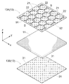
- FIG. 2 is a development view of the transparent electrode 13 corresponding to one pixel of the liquid crystal display device 100
- FIG. 3 is an enlarged front view of a part thereof.
- the alignment film 12 is omitted in FIGS. 2 and 3, and a pair of transparent electrodes 13A and 13B and a liquid crystal layer 11 are shown.
- the transparent electrode 13A will be described as the first transparent electrode 13A
- the transparent electrode 13B will be described as the second transparent electrode 13B.
- a first slit 21 is formed as an opening for opening the first transparent electrode 13A having a predetermined width. Accordingly, the first slit 21 does not act as the first transparent electrode 13A.
- the first transparent electrode 13A is provided with a plurality of unit regions S that are surrounded by the first slit 21 in six directions.
- the unit region S surrounded by the six directions corresponds to a region formed in a regular hexagon in the present embodiment. Accordingly, the six directions correspond to directions orthogonal to the sides of the regular hexagon.
- the unit area S has a polygonal shape.
- each of the two opposing slit portions is parallel to the pixel edge 92 parallel to the y-axis direction defining one pixel.
- a first slit 21 is provided.
- a plurality of unit regions S having such a regular hexagonal shape are formed in the first transparent electrode 13A.
- the adjacent unit regions S are configured to share a part of the slit. Therefore, the unit region S according to the present embodiment is configured in a honeycomb shape. Note that in the vicinity of the pixel edge 91 in the x-axis direction and the pixel edge 92 in the y-axis direction that define one pixel, the unit region S does not maintain a regular hexagon and is partially cut out.
- the discontinuous part 22 is provided in such a 1st slit 21, and adjacent unit area
- region S is connected by the connection part of at least one place.
- the adjacent unit regions S are configured to share a part of the slit.
- the discontinuous portion 22 is provided in some of the shared slits. Therefore, the slit provided with the discontinuous portion 22 is configured to be shorter than the other slits. With this configuration, a continuous pattern in which the first slits 21 provided with the discontinuous portions 22 are continuously arranged is formed on the first transparent electrode 13A.
- the unit regions S are arranged in parallel, two discontinuous portions 22 are provided for each unit region S.
- the first transparent electrode 13A for one pixel when a pair of unit regions S adjacent in a predetermined direction is seen, all the discontinuous portions 22 included in the pair of unit regions S are linearly arranged. That is, when the first transparent electrode 13A for one pixel is a square as shown in FIG. 2, the direction in which the unit region S is adjacent corresponds to the diagonal direction. Accordingly, the discontinuous portions 22 of all the unit regions S for one pixel are arranged in parallel to one diagonal direction.
- the 1st slit 21 in 1 pixel can be comprised by the same shape. Therefore, the first slit 21 can be easily formed. Therefore, the manufacturing cost of the first transparent electrode 13A can be reduced.
- the second transparent electrode 13B is provided with a second slit 31 at a position that does not overlap with the first slit 21 when viewed in the thickness direction of the liquid crystal layer 11.
- the thickness direction of the liquid crystal layer 11 is the z-axis direction orthogonal to the first transparent electrode 13A and the second transparent electrode 13B.
- the second slit 31 is provided so as not to overlap the first slit 21 when the first transparent electrode 13A and the second transparent electrode 13B are viewed from the z-axis direction.
- the second slit 31 is configured by a dot-like region provided at a position corresponding to the center of each unit region S when viewed in the direction along the thickness direction of the liquid crystal layer 11 (z-axis direction).
- the second slit 31 is preferably configured in a shape similar to the unit region S.
- the 2nd slit 31 is comprised by the shape of a regular hexagon. With this configuration, the distance between the first slit 21 and the second slit 31 can be made substantially uniform except for the discontinuous portion 22 in all directions when viewed in the z-axis direction.
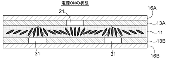
- an electric field can be uniformly generated in the liquid crystal layer 11 when a voltage is applied to the first transparent electrode 13A and the second transparent electrode 13B. Therefore, before the voltage is applied to the first transparent electrode 13A and the second transparent electrode 13B, the liquid crystal molecules in the liquid crystal layer 11 are vertically aligned as shown in FIG. In this case, as shown in FIG. 5, the second slits 31 can be oriented radially. Therefore, the viewing angle can be widened and the contrast can be increased.
- the visual characteristics of the liquid crystal display device 100 configured as described above were evaluated.
- the evaluation result of the visual characteristic will be described using an isocontrast curve.
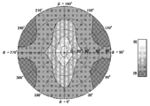
- the iso-contrast curve is one of the methods for showing the visual characteristics of the screen (display), and is a graph in which the contrast when the screen is observed from various angles is plotted and the same contrast value is connected by a line.
- the contrast is expressed by Ton (transmittance for ON display) / Toff (transmittance for OFF display).
- the isocontrast curve is shown by a pie chart defined by an angle ⁇ and an angle ⁇ as shown in FIG.
- the angle ⁇ is an angle formed between the line of sight and the normal line of the screen
- the angle ⁇ is an angle formed between the line of sight projected on the xy plane and the y axis.
- the line of sight is a straight line connecting the observation position and the center point of the liquid crystal display device 100, and x and y axes are set on the surface of the liquid crystal display device 100.
- the angle (radial radius) defined on the outer periphery of the pie chart corresponds to the angle ⁇
- the angle (radius) defined inside the pie chart corresponds to the angle ⁇ .
- ⁇ was evaluated as 0 ° ⁇ ⁇ ⁇ 80 °, and ⁇ was evaluated as 0 ° ⁇ ⁇ ⁇ 360 °.
- the writing cycle of one line on the screen was set to 1/64 cycle.
- FIG. 7 shows an isocontrast curve according to this embodiment.
- a first slit configured so that the unit region is a square
- a second slit configured with a square at a position not overlapping with the first slit when viewed in the thickness direction of the liquid crystal layer 11 are included.
- FIG. 9 shows an isocontrast curve of the liquid crystal display device of the embodiment (FIG. 10).
- the liquid crystal display device 100 according to the present embodiment has a substantially concentric curve with an isocontrast curve. Therefore, it is understood that the liquid crystal display device 100 according to the present embodiment has a wide viewing angle, uniform contrast, and favorable viewing angle characteristics. Further, it was found that the transmittance Ton in the front view was 1.6% in the liquid crystal display device of the reference form, but was greatly improved to 3.7% in the liquid crystal display device 100 of the present embodiment. .
- the unit region S of the first transparent electrode 13A is formed in a honeycomb shape, and the second slit 31 is formed in a dotted region.
- the unit region S and the second slit 31 according to the present embodiment are formed in a shape different from the shape of the first embodiment.
- it demonstrates using drawing.
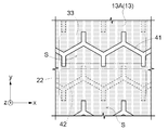
- FIGS. 12 and 13 are schematic views of the transparent electrode 13.
- FIG. 12 shows a developed view of the transparent electrode 1 corresponding to one pixel of the liquid crystal display device 100
- FIG. 13 shows a partially enlarged front view.
- the alignment film 12 is omitted in FIGS. 12 and 13, and only a pair of transparent electrodes 13A and 13B are shown.
- the transparent electrode 13A will be described as the first transparent electrode 13A
- the transparent electrode 13B will be described as the second transparent electrode 13B.
- the first continuous slit 41 is arranged in parallel on the first transparent electrode 13A according to the present embodiment.
- the first continuous slit 41 divides the first slit 21 forming the unit region S by arranging the discontinuous portions 22 in a straight line, and is divided on the same side with respect to the straight discontinuous portions 22.
- the other first slits 21 are connected to each other.
- disposing the discontinuous portions 22 in a straight line means disposing the discontinuous portions 22 in a straight line along the x-axis for one pixel. Therefore, when the first transparent electrode 13A is viewed along the x-axis, there is a region where the first slit 21 is not formed between the first end and the second end in the x-axis direction.
- This region is a discontinuous portion 22.
- the first slit 21 is divided into two along the y-axis direction, and the first continuous slit 41 is configured by connecting the first slits 21 adjacent in the x-axis direction to each other.
- the first slit 21 corresponds to a regular hexagon divided into two.
- the second slit 31 has the same shape as the first continuous slit 41. However, the second slit 31 is juxtaposed at a position that does not overlap with the first continuous slit 41 in the thickness direction of the liquid crystal layer 11.
- the thickness direction view of the liquid crystal layer 11 indicates a state viewed from the z-axis direction.
- the second slit 31 is also formed with a linear discontinuous portion 33.
- the second continuous slit 42 is formed by connecting the second slits 31 which are divided by the discontinuous portion 33 and are in the same direction with respect to the discontinuous portion 33.
- the second continuous slit 42 is disposed so as not to overlap the first continuous slit 41 when viewed in the z-axis direction.
- the second slit 31 is arranged with a position shifted in the x-axis direction by half the length of the first slit 21 in the x-axis direction with respect to the first slit 21. Accordingly, the first continuous slit 41 and the second continuous slit 42 so that the first continuous slit 41 and the discontinuous portion 33 overlap and the second continuous slit 42 and the discontinuous portion 22 overlap when viewed in the z-axis direction. And are arranged.
- the distance between the first slit 21 and the second slit 31 can be made substantially equal when viewed in the z-axis direction as in the first embodiment. Therefore, when a voltage is applied to the first transparent electrode 13A and the second transparent electrode 13B, the electric field strength generated between the first transparent electrode 13A and the second transparent electrode 13B can be made uniform. Therefore, the liquid crystal molecules in the liquid crystal layer 11 are uniformly aligned, the viewing angle can be widened, and the contrast can be increased.
- FIG. 14 shows an isocontrast curve according to the present embodiment.
- the isocontrast curve is substantially concentric. Therefore, it is understood that the liquid crystal display device 100 according to the present embodiment also has a wide viewing angle, uniform contrast, and favorable viewing angle characteristics. Moreover, it turned out that the transmittance
- the first transparent electrode 13A and the second transparent electrode 13B according to the present embodiment are also properly oriented. I understood. Furthermore, it turned out that it is oriented efficiently and has a bright display.
- the unit region S has a regular hexagonal shape.
- the scope of application of the present invention is not limited to this.
- the unit region S may be formed in a shape such as a hexagon other than a regular hexagon.
- the second slit 31 is formed in a regular hexagonal shape.
- the scope of application of the present invention is not limited to this.
- the second slit 31 may be formed in a shape other than a regular hexagon such as a hexagon, a circle, or another polygon.
- 16 and 17 show a modification of the second embodiment.
- a side parallel to the y-axis is extended in the y-axis direction among the first slit and the second slit 31 of the second embodiment.
- the first slit 21 and the second slit 31 have the same slit length parallel to the y-axis direction and are adjacent to each other in parallel to the y-axis direction.
- the slits between the first slit 31 and the second slit 31 overlap each other over the entire length when viewed in the x-axis direction. Even in such a configuration, the viewing angle can be widened and the contrast can be increased.
- FIG. 18 shows an isocontrast curve relating to the liquid crystal display device 100 when the first slit 21 and the second slit 31 are formed in this manner.
- the first slit 21 and the second slit 31 are concentric with respect to the isocontrast curve of FIG. It is understood that the viewing angle characteristic is good.
- permeability Ton in the front view of such a liquid crystal display device 100 is greatly improved with 3.0%.
- the first transparent electrode 13A and the second transparent electrode 13B according to the present embodiment are also properly oriented. I understood. Furthermore, it turned out that it is oriented efficiently and has a bright display.
- discontinuous portions 22 are provided in the unit region S.
- the discontinuous portion 22 can be provided at one place, and can be provided at three or more places.
- the plurality of discontinuous portions 22 are arranged linearly.
- the scope of application of the present invention is not limited to this.
- the second slit 31 is provided at a position corresponding to the center of the unit region S when viewed in the z-axis direction.
- the scope of application of the present invention is not limited to this.
- the absorption axis of the polarizing plate 16A is set in parallel to the first direction of a pair of diagonal lines in one pixel defined by the pixel edge 91 in the x-axis direction and the pixel edge 92 in the y-axis direction
- the absorption axis of the polarizing plate 16B was set parallel to the second direction of the pair of diagonal lines.
- the scope of application of the present invention is not limited to this.
- the absorption axes of the polarizing plates 16A and 16B can be set along a direction that is not parallel to the diagonal line.
- the present invention can be used for a vertical alignment type liquid crystal display device including a liquid crystal layer and a pair of transparent electrodes sandwiching the liquid crystal layer.
- liquid crystal display device S unit region
Landscapes
- Physics & Mathematics (AREA)
- Nonlinear Science (AREA)
- Mathematical Physics (AREA)
- Chemical & Material Sciences (AREA)
- Crystallography & Structural Chemistry (AREA)
- General Physics & Mathematics (AREA)
- Optics & Photonics (AREA)
- Liquid Crystal (AREA)
- Geometry (AREA)
- Spectroscopy & Molecular Physics (AREA)
Abstract
液晶層11と、液晶表示層11を挟む第1透明電極13Aおよび第2透明電極と、を備えた垂直配向型の液晶表示装置は、第1透明電極13Aに、第1スリット21を備え、第1スリット21で6方向が囲まれた単位領域Sが複数並設されている。第1スリット21は、隣接する単位領域Sどうしが少なくとも一箇所の接続部で連接されて連続パターンを形成するように不連続部22を備えている。第2透明電極13Bは、液晶層11の厚み方向に沿う方向視で第1スリット21と重複しない位置に第2スリット31を備えている。
Description
本発明は、液晶層と液晶層を挟む一対の透明電極とを備えた垂直配向型の液晶表示装置に関する。
従来、視野角を広げると共にコントラストを高めた表示装置として、VA(Vertical Alignment:垂直配向)型の液晶ディスプレイが利用されてきた。更に視野角を広げたPMVA(Pattern Multi Vertical Alignment)型も利用されている。この種の技術として特許文献1及び2に記載のものがある。
特許文献1に記載の液晶表示素子は、一対の透明電極に第1スリット部と第2スリット部とを備えている。互いに直交するX軸及びY軸で規定された表示領域に対して、第1スリット部はX軸に対し傾斜した方向に長手となっており、第2スリット部はX軸に対し第1スリット部とは反対方向に傾斜した方向に長手となるように構成される。第1の透明電極の第1スリット部と第2の透明電極の第1スリット部とがY軸方向に交互に配置されると共に、第1の透明電極の第2スリット部と第2の透明電極の第2スリット部とがY軸方向に交互に配置される。
また、特許文献2に記載の広視野角液晶表示装置は、互いに対向して配置される第1電極及び第2電極に、それぞれ複数の第1開口部及び複数の第2開口部が形成される。この第1開口部及び第2開口部は、厚み方向に見た場合、閉じた閉曲線を形成するように構成される。
特許文献1及び2に記載の技術では、透明電極の通電時の開口率が低いのでコントラストを高くすることができない。更には、効率も悪くなり省エネルギー化を図ることができない。また、配向安定性も悪く、更に視野角を広げることは容易ではない。
本発明の目的は、上記問題に鑑み、視野角が広く、コントラストが高い液晶表示装置を提供することにある。
本発明に係る液晶表示装置の実施形態の一つでは、液晶層と、前記液晶層を挟む第1透明電極および第2透明電極と、を備えた垂直配向型であり、前記第1透明電極は、第1スリットを備えるとともに、当該第1スリットで6方向が囲まれた単位領域が複数並設され、前記第1スリットは、隣接する前記単位領域どうしが少なくとも一箇所の接続部で連接されて連続パターンを形成するように不連続部を備え、前記第2透明電極は、前記液晶層の厚み方向に沿う方向視で前記第1スリットと重複しない位置に第2スリットを備えている。
このような特徴構成とすれば、液晶分子を単位領域によって主に6方向に配向させることができるので、視野角を広げることができる。更には、開口率を高くすることができるので、コントラストも高めることが可能となる。
また、前記単位領域の形状を多角形形状とすると好適である。
単位領域の形状が多角形であれば、液晶分子を多くの方向に沿って配向させることが可能となる。
また、前記単位領域は二箇所の前記不連続部を備え、一対の前記単位領域が有する前記不連続部が直線状に配置されていると好適である。
このような構成とすれば、複数の単位領域の形状を同一のものとすることができる。したがって、製造工程を簡素化することができるので、製造コストを低減できる。また、各単位領域を横断する状態に通電できるので、各単位領域の通電状態を一様にすることができる。
また、前記第2スリットが、前記液晶層の厚み方向に沿う方向視で夫々の前記単位領域の中央に対応する位置に設けられた点状領域とすると好適である。
このような構成とすれば、第1透明電極と第2透明電極とが対向する領域の面積を広くすることができると共に、第1透明電極と第2透明電極との間に生じる電界の強度が著しく弱い部分が生じなくすることができる。したがって、液晶分子の配向を適切に変更することできる。
或いは、前記不連続部を直線状に配置することで前記単位領域を形成する前記第1スリットを分割し、前記不連続部に対して同一側にある前記分割された第1スリットどうしを連接して構成した第1連続スリットを並設しても良い。
このような構成であっても、複数の単位領域の形状を同一のものとすることができる。したがって、製造工程を簡素化することができるので、製造コストを低減できる。また、各単位領域を横断する状態に通電できるので、各単位領域の通電状態を一様にすることができる。
また、前記第2スリットが、前記第1連続スリットと同じ形状であり、前記液晶層の厚み方向視において、前記第1連続スリットと重複しない位置に並設されてあると好適である。
このような構成であっても、第1透明電極と第2透明電極とが対向する領域の面積を広くすることができるので、第1透明電極と第2透明電極との間に生じる電界の強度が著しく弱い部分が生じなくすることができる。したがって、液晶分子の配向を適切に変更することできる。
以下、本発明の実施の形態について図面に基づいて詳細に説明する。図1は本実施形態に係る液晶表示装置100の構成を模式的に示した図である。液晶表示装置100は液晶層とその液晶層を挟む一対の透明電極とを備えた垂直配向型であり、視野角が広く、コントラストが高い特性を有するように構成される。
〔液晶表示装置の全体構成〕
図1に示されるように、液晶表示装置100は、液晶層11、配向膜12、透明電極13、ガラス基板15、偏光板16、バックライト17を備えて構成される。
図1に示されるように、液晶表示装置100は、液晶層11、配向膜12、透明電極13、ガラス基板15、偏光板16、バックライト17を備えて構成される。
液晶層11は有機物の一種の液体である液晶材料からなる。この液晶材料は、棒状又は円盤状等の液晶分子を含んで構成される。液晶分子は、当該液晶分子の長軸方向に対して長距離秩序を有する。これにより、液晶材料は、液体でありながら固体と同様の規則正しい分子配列を有することができる。配向膜12は一対の配向膜12A、12Bからなり、液晶層11を挟持する。配向膜12は、液晶分子の長軸方向が無通電状態において配向膜12A及び配向膜12Bの対向方向に沿うように液晶分子を配列させる。
透明電極13は一対の透明電極13A、13Bからなり、上述の液晶層11を挟持している状態の配向膜12を更に外側から挟持する。透明電極13は、液晶表示装置100を駆動させる電極に相当する。透明電極13に通電することにより電界が生じ、その電界によって液晶分子の配向が変更される。透明電極13は、液晶表示装置100としての表示の妨げとならないように、透明度の高い材料で構成される。
このような構造で構成される構造体の両側には、一対のガラス基板15(15A、15B)が設けられる。これにより、透明電極13を他の導電物から絶縁する。更に一対のガラス基板15のそれぞれの外側には、偏光板16が設けられる。したがって、偏光板16も一対の偏光板16A、16Bからなる。偏光板16は、入射光に対して特定の光のみを透過させるように所定の吸収軸が設定される。本実施形態では、偏光板16Aの吸収軸は、x軸方向の画素エッジ91(図2参照)及びy軸方向の画素エッジ92(図2参照)で規定された1画素における一対の対角線のうちの第1方向に平行に設定される。また、偏光板16Bの吸収軸は、前記一対の対角線のうちの第2方向に平行に設定される。
偏光板16Bの外側には、バックライト17が設けられる。バックライト17は、表示面を背面から均一に照射する。本発明に係る液晶表示装置100はこのような構造で構成される。
〔透明電極の構成の第1の実施形態〕
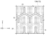
次に、透明電極13の構成について説明する。図2,3には、透明電極13の模式図が示される。図2は液晶表示装置100の1画素に対応する透明電極13の展開図が示され、図3はその一部を拡大した正面視が示される。理解を容易にするために、図2,3においては配向膜12は省略し、一対の透明電極13A,13Bと液晶層11が示される。本実施形態では、透明電極13Aを第1透明電極13Aとし、透明電極13Bを第2透明電極13Bとして説明する。
次に、透明電極13の構成について説明する。図2,3には、透明電極13の模式図が示される。図2は液晶表示装置100の1画素に対応する透明電極13の展開図が示され、図3はその一部を拡大した正面視が示される。理解を容易にするために、図2,3においては配向膜12は省略し、一対の透明電極13A,13Bと液晶層11が示される。本実施形態では、透明電極13Aを第1透明電極13Aとし、透明電極13Bを第2透明電極13Bとして説明する。
第1透明電極13Aには、所定の幅からなる第1透明電極13Aを開口する開口部としての第1スリット21が形成されている。したがって、第1スリット21は、第1透明電極13Aとしては作用しない。また、第1透明電極13Aには、第1スリット21で6方向が囲まれた単位領域Sが複数並設される。6方向が囲まれた単位領域Sとは、本実施形態では正六角形で形成される領域が相当する。したがって、6方向とは正六角形の各辺に直交する方向が相当する。これにより、単位領域Sは、多角形形状を有することになる。ここで、一つの単位領域Sを形成する第1スリット21のうち、対向する2つのスリット部分が、1画素を規定するy軸方向に平行な画素エッジ92に対して平行となるように、各第1スリット21が設けられる。
第1透明電極13Aには、このような正六角形の形状からなる単位領域Sが複数構成される。この際、互いに隣接する単位領域Sは、スリットの一部を共有して構成される。したがって、本実施形態に係る単位領域Sは、ハニカム状に構成される。なお、1画素を規定するx軸方向の画素エッジ91及びy軸方向の画素エッジ92の近傍においては、単位領域Sは正六角形を維持せず一部が切り欠かれた形状とされる。
また、このような第1スリット21には不連続部22が設けられ、隣接する単位領域Sどうしが少なくとも一箇所の接続部で連接される。上述のように、互いに隣接する単位領域Sは、スリットの一部を共有して構成される。不連続部22は、共有される一部のスリットに設けられる。したがって、不連続部22が設けられるスリットは、他のスリットよりも短く構成される。このように構成されることにより、第1透明電極13Aには、不連続部22が設けられた第1スリット21を連続して配置した連続パターンが形成される。
また、図2に示されるように、単位領域Sが並設されることから、一つの単位領域Sにつき不連続部22が二箇所設けられる。1画素分の第1透明電極13Aにおいて、所定方向に隣接する一対の単位領域Sをみたとき、一対の単位領域Sが有する全ての不連続部22が直線状に配置される。すなわち、1画素分の第1透明電極13Aが、図2に示されるように正方形からなる場合には、単位領域Sが隣接する方向とは対角線の方向が相当する。したがって、1画素分における全ての単位領域Sの不連続部22が、一方の対角線の方向に平行に配置される。このように構成することにより、1画素分における第1スリット21を同一形状で構成することができる。そのため、第1スリット21を容易に形成することができる。したがって、第1透明電極13Aの製造コストを低減できる。
第2透明電極13Bには、液晶層11の厚み方向に沿う方向視で第1スリット21と重複しない位置に第2スリット31が備えられる。液晶層11の厚み方向とは、第1透明電極13A及び第2透明電極13Bに直交するz軸方向である。第2スリット31は、第1透明電極13A及び第2透明電極13Bをz軸方向から見て第1スリット21に重複しないように設けられる。
本実施形態では、第2スリット31は、液晶層11の厚み方向に沿う方向(z軸方向)視で単位領域Sの夫々の中央に対応する位置に設けた点状領域で構成される。第2スリット31は、単位領域Sに相似する形状で構成すると好適である。本実施形態の場合、第2スリット31は正六角形の形状で構成される。このように構成することにより、z軸方向視において、第1スリット21と第2スリット31との間隔を全方位に亘って、不連続部22を除いて略均等にすることができる。
このように構成することにより、第1透明電極13Aと第2透明電極13Bとに電圧を印加した場合には、液晶層11内に一様に電界を生じさせることができる。したがって、第1透明電極13Aと第2透明電極13Bとに電圧を印加する前には、図4に示されるように、液晶層11内の液晶分子が垂直配向していたものが、電圧を印加した場合には、図5に示されるように、第2スリット31を中心として放射状に配向させることができる。このため、視野角を広くすることができると共に、コントラストも高めることが可能となる。
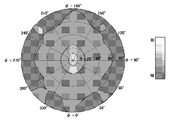
上記のように構成した液晶表示装置100について、視覚特性の評価を行った。以下では、視覚特性の評価結果について等コントラスト曲線を用いて説明する。等コントラスト曲線とは、画面(ディスプレイ)の視覚特性を示す手法の一つであり、画面を様々な角度から観察した時のコントラストをプロットし、同一のコントラスト値を線で結んだグラフである。ここで、コントラストは、Ton(ON表示の透過率)/Toff(OFF表示の透過率)で示される。
等コントラスト曲線は、図7に示されるような、角θと角φとで規定された円グラフで示される。ここで、角θは、視線と画面の法線とのなす角度であり、角φは、xy平面上に投影した視線とy軸とがなす角度である。なお、視線とは、観察位置と液晶表示装置100の中心点とを結ぶ直線であり、液晶表示装置100の表面にx,y軸が設定されている。円グラフの外周に規定された角度(動径)が角φに対応し、円グラフの内部に規定された角度(半径)が角θに対応する。今回は、θは0°≦θ<80°とし、φは0°≦φ≦360°として評価した。また、評価条件としては、画面の1ラインの書き込み周期を1/64周期とした。
本実施形態に係る等コントラスト曲線が、図7に示される。一方、参考として、単位領域が正方形となるように構成した第1スリットと、液晶層11の厚み方向に沿う方向視で第1スリットと重複しない位置に正方形で構成した第2スリットと、有する参考形態の液晶表示装置(図10)の等コントラスト曲線が図9に示される。図7及び図9から明らかなように、本実施形態における液晶表示装置100の方が、等コントラスト曲線が略同心円状である。したがって、本実施形態における液晶表示装置100は、視野角が広く、コントラストも一様であり、良好な視野角特性であることが理解される。また、正面視における透過率Tonは、参考形態の液晶表示装置では1.6%であったものが、本実施形態の液晶表示装置100では3.7%と大きく改善されていることがわかった。
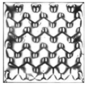
また、このような液晶表示装置100のON画素を確認したところ、本実施形態に係る第1透明電極13A及び第2透明電極13Bでも、適切に配向していることがわかった。更に、参考形態(図11)に係るものよりも、本実施形態のもの(図8)の方が効率良く配向されており、明るい表示となっていることがわかった。
〔透明電極の構成の第2の実施形態〕
上述の第1の実施形態では、第1透明電極13Aの単位領域Sがハニカム状に形成され、第2スリット31が点状領域で形成されていた。本実施形態に係る単位領域S及び第2スリット31は、第1の実施形態の形状とは異なる形状で形成される。以下、図面を用いて説明する。
上述の第1の実施形態では、第1透明電極13Aの単位領域Sがハニカム状に形成され、第2スリット31が点状領域で形成されていた。本実施形態に係る単位領域S及び第2スリット31は、第1の実施形態の形状とは異なる形状で形成される。以下、図面を用いて説明する。
図12,13には、透明電極13の模式図が示される。図12は液晶表示装置100の1画素に対応する透明電極1の展開図が示され、図13はその一部を拡大した正面視が示される。理解を容易にするために、図12,13においては配向膜12は省略し、一対の透明電極13A,13Bのみが示される。本実施形態では、透明電極13Aを第1透明電極13Aとし、透明電極13Bを第2透明電極13Bとして説明する。
本実施形態に係る第1透明電極13Aには、第1連続スリット41が並設されている。第1連続スリット41は、不連続部22を直線状に配置することで単位領域Sを形成する第1スリット21を分割し、直線状の不連続部22に対して同一方側にある分割された一方の第1スリット21どうしを連接して構成されている。本実施形態では、不連続部22を直線状に配置するとは、不連続部22を1画素分におけるx軸に沿って直線状に配置することを意味する。したがって、第1透明電極13Aをx軸に沿って見た場合、x軸方向の第1端部と第2端部との間にわたって第1スリット21が形成されていない領域がある。この領域が不連続部22である。このように構成することにより、第1スリット21がy軸方向に沿って2つに分割され、x軸方向に隣接する第1スリット21どうしを互いに連接して第1連続スリット41が構成される。ここで、本実施形態では、第1スリット21は、正六角形を2つに分割したものが相当する。
また、第2スリット31は、第1連続スリット41と同じ形状である。ただし、第2スリット31は、液晶層11の厚み方向視において、第1連続スリット41と重複しない位置に並設されている。液晶層11の厚み方向視とは、z軸方向から見た状態を示す。第2スリット31も、また、第1スリット21と同様に、直線状の不連続部33が形成されている。この不連続部33により分割され、不連続部33に対して同一方向にある第2スリット31どうしを連接して第2連続スリット42が形成される。この第2連続スリット42は、z軸方向視において、第1連続スリット41と重複しないように配置される。すなわち、第2スリット31は、第1スリット21に対して当該第1スリット21のx軸方向の長さの半分だけ、x軸方向に位置をずらして配置される。したがって、z軸方向視において第1連続スリット41と不連続部33とが重複し、第2連続スリット42と不連続部22とが重複するように、第1連続スリット41と第2連続スリット42とが配置される。
このように構成することにより、上記第1の実施形態と同様に、z軸方向視において、第1スリット21と第2スリット31との距離を略均等にすることができる。そのため、第1透明電極13Aと第2透明電極13Bとに電圧を印加した場合、第1透明電極13Aと第2透明電極13Bとの間に生じる電界強度を一様にすることができる。したがって、液晶層11内の液晶分子が一様に配向し、視野角を広くすることができ、またコントラストも高くすることができる。
本実施形態に係る等コントラスト曲線が、図14に示される。図15から明らかなように、本実施形態における液晶表示装置100であっても、等コントラスト曲線が略同心円状となっている。そのため、本実施形態における液晶表示装置100も、視野角が広く、コントラストも一様であり、良好な視野角特性であることが理解される。また、本実施形態における液晶表示装置100の正面視における透過率Tonは、3.2%と大きく改善されていることがわかった。
また、このような液晶表示装置100のON画素を確認したところ、図15に示されるように、本実施形態に係る第1透明電極13A及び第2透明電極13Bでも、適切に配向していることがわかった。更に、効率良く配向されており、明るい表示となっていることがわかった。
〔その他の実施形態〕
上記実施形態では、単位領域Sを正六角形の形状とした。しかしながら、本発明の適用範囲はこれに限定されるものではない。単位領域Sを正六角形以外の六角形などの形状で構成することも当然に可能である。
上記実施形態では、単位領域Sを正六角形の形状とした。しかしながら、本発明の適用範囲はこれに限定されるものではない。単位領域Sを正六角形以外の六角形などの形状で構成することも当然に可能である。
上記第1の実施形態では、第2スリット31を正六角形の形状で構成した。しかしながら、本発明の適用範囲はこれに限定されるものではない。第2スリット31を例えば六角形や円形、他の多角形のような正六角形以外の形状で構成することも可能である。
図16,17は、第2の実施形態の変形例を示している。この変形例では、第2の実施形態の第1スリットおよび第2スリット31のうち、y軸に平行な辺をy軸方向に延長している。このように延長した場合でも、第1透明電極13A及び第2透明電極13Bのz軸方向視において、第1スリット21と第2スリット31とが重複しないように構成すると好適である。また、図17に示されるように、第1スリット21と第2スリット31とのy軸方向に平行なスリットの長さが互いに等しく、且つ、このy軸方向に平行で隣接する第1スリット21と第2スリット31とのスリットが、x軸方向視で全長に亘って重複するように構成すると好適である。このように構成した場合でも、視野角を広くすることができると共に、コントラストも高めることが可能となる。
このように第1スリット21及び第2スリット31を形成した場合の液晶表示装置100に係る等コントラスト曲線が、図18に示される。図18から明らかなように、このような第1スリット21及び第2スリット31であっても、図9の等コントラスト曲線に比べて同芯円状であるので、このような液晶表示装置100は良好な視野角特性であることが理解される。また、このような液晶表示装置100の正面視における透過率Tonは、3.0%と大きく改善されていることがわかった。
また、このような液晶表示装置100のON画素を確認したところ、図19に示されるように、本実施形態に係る第1透明電極13A及び第2透明電極13Bでも、適切に配向していることがわかった。更に、効率良く配向されており、明るい表示となっていることがわかった。
上記実施形態では、単位領域Sに不連続部22が二箇所設けられていた。しかしながら、本発明の適用範囲はこれに限定されるものではない。不連続部22を一箇所とすることも可能であるし、三箇所以上とすることも当然に可能である。
上記実施形態では、複数の不連続部22が直線状に配置されていた。しかしながら、本発明の適用範囲はこれに限定されるものではない。複数の不連続部22を非直線状に配置することも当然に可能である。
上記第1の実施形態では、第2スリット31がz軸方向視において単位領域Sの中央に対応する位置に設けられていた。しかしながら、本発明の適用範囲はこれに限定されるものではない。第2スリット31を単位領域Sの中央以外の位置に対応する位置に配置することも当然に可能である。
上記実施形態では、偏光板16Aの吸収軸は、x軸方向の画素エッジ91及びy軸方向の画素エッジ92で規定された1画素における一対の対角線のうちの第1方向に平行に設定され、偏光板16Bの吸収軸は、前記一対の対角線のうちの第2方向に平行に設定されていた。しかしながら、本発明の適用範囲はこれに限定されるものではない。偏光板16A、16Bの吸収軸は、対角線に対して平行でない方向に沿って設定することも当然に可能である。
本発明は、液晶装層と液晶層を挟む一対の透明電極とを備えた垂直配向型の液晶表示装置に利用することが可能である。
11:液晶層
13:透明電極
13A:第1透明電極
13B:第2透明電極
21:第1スリット
22:不連続部
31:第2スリット
100:液晶表示装置
S:単位領域
13:透明電極
13A:第1透明電極
13B:第2透明電極
21:第1スリット
22:不連続部
31:第2スリット
100:液晶表示装置
S:単位領域
Claims (6)
- 液晶層と、前記液晶層を挟む第1透明電極および第2透明電極と、を備えた垂直配向型の液晶表示装置であって、
前記第1透明電極は、第1スリットを備えるとともに、当該第1スリットで6方向が囲まれた単位領域が複数並設され、
前記第1スリットは、隣接する前記単位領域どうしが少なくとも一箇所の接続部で連接されて連続パターンを形成するように不連続部を備え、
前記第2透明電極は、前記液晶層の厚み方向に沿う方向視で前記第1スリットと重複しない位置に第2スリットを備えている液晶表示装置。 - 前記単位領域は多角形形状を有する請求項1に記載の液晶表示装置。
- 前記単位領域は二箇所の前記不連続部を備え、
一対の前記単位領域が有する前記不連続部が直線状に配置されている請求項1又は2に記載の液晶表示装置。 - 前記第2スリットが、前記液晶層の厚み方向に沿う方向視で夫々の前記単位領域の中央に対応する位置に設けられた点状領域である請求項1から3の何れか一項に記載の液晶表示装置。
- 前記単位領域は、直線状に配置された前記不連続部によって分割され、
前記不連続部に対して同一側にある前記分割された第1スリットどうしを連接して構成した第1連続スリットを並設してある請求項3に記載の液晶表示装置。 - 前記第2スリットが、前記第1連続スリットと同じ形状であり、前記液晶層の厚み方向視において、前記第1連続スリットと重複しない位置に並設されてある請求項5に記載の液晶表示装置。
Applications Claiming Priority (2)
| Application Number | Priority Date | Filing Date | Title |
|---|---|---|---|
| JP2011248813A JP2013105031A (ja) | 2011-11-14 | 2011-11-14 | 液晶表示装置 |
| JP2011-248813 | 2011-11-14 |
Publications (1)
| Publication Number | Publication Date |
|---|---|
| WO2013073312A1 true WO2013073312A1 (ja) | 2013-05-23 |
Family
ID=48429382
Family Applications (1)
| Application Number | Title | Priority Date | Filing Date |
|---|---|---|---|
| PCT/JP2012/075946 Ceased WO2013073312A1 (ja) | 2011-11-14 | 2012-10-05 | 液晶表示装置 |
Country Status (3)
| Country | Link |
|---|---|
| JP (1) | JP2013105031A (ja) |
| TW (1) | TW201331685A (ja) |
| WO (1) | WO2013073312A1 (ja) |
Families Citing this family (1)
| Publication number | Priority date | Publication date | Assignee | Title |
|---|---|---|---|---|
| JP7067599B1 (ja) * | 2020-11-17 | 2022-05-16 | 凸版印刷株式会社 | 調光シート及び調光シートの製造方法 |
Citations (5)
| Publication number | Priority date | Publication date | Assignee | Title |
|---|---|---|---|---|
| JP2002287158A (ja) * | 2000-12-15 | 2002-10-03 | Nec Corp | 液晶表示装置およびその製造方法ならびに駆動方法 |
| JP2003043525A (ja) * | 2000-08-11 | 2003-02-13 | Sharp Corp | 液晶表示装置 |
| JP2004177788A (ja) * | 2002-11-28 | 2004-06-24 | Hitachi Displays Ltd | 液晶表示装置 |
| WO2005111708A1 (ja) * | 2004-05-18 | 2005-11-24 | Sharp Kabushiki Kaisha | 液晶表示装置およびそれを備えた電子機器 |
| JP2006234871A (ja) * | 2005-02-22 | 2006-09-07 | Sanyo Epson Imaging Devices Corp | 液晶装置、及び電子機器 |
-
2011
- 2011-11-14 JP JP2011248813A patent/JP2013105031A/ja active Pending
-
2012
- 2012-10-05 WO PCT/JP2012/075946 patent/WO2013073312A1/ja not_active Ceased
- 2012-10-17 TW TW101138247A patent/TW201331685A/zh unknown
Patent Citations (5)
| Publication number | Priority date | Publication date | Assignee | Title |
|---|---|---|---|---|
| JP2003043525A (ja) * | 2000-08-11 | 2003-02-13 | Sharp Corp | 液晶表示装置 |
| JP2002287158A (ja) * | 2000-12-15 | 2002-10-03 | Nec Corp | 液晶表示装置およびその製造方法ならびに駆動方法 |
| JP2004177788A (ja) * | 2002-11-28 | 2004-06-24 | Hitachi Displays Ltd | 液晶表示装置 |
| WO2005111708A1 (ja) * | 2004-05-18 | 2005-11-24 | Sharp Kabushiki Kaisha | 液晶表示装置およびそれを備えた電子機器 |
| JP2006234871A (ja) * | 2005-02-22 | 2006-09-07 | Sanyo Epson Imaging Devices Corp | 液晶装置、及び電子機器 |
Also Published As
| Publication number | Publication date |
|---|---|
| TW201331685A (zh) | 2013-08-01 |
| JP2013105031A (ja) | 2013-05-30 |
Similar Documents
| Publication | Publication Date | Title |
|---|---|---|
| US11320680B2 (en) | Viewing angle switch module and display apparatus | |
| CN103513470B (zh) | 液晶显示器 | |
| JP4439581B2 (ja) | 表示装置 | |
| JP4812825B2 (ja) | 表示装置 | |
| JP4846402B2 (ja) | 液晶表示素子 | |
| US9250477B2 (en) | Array substrate and liquid crystal display | |
| CN104199225A (zh) | 一种显示面板及其制作方法、以及显示装置 | |
| GB2433640A (en) | Display device for displaying single or dual images | |
| KR101431676B1 (ko) | 액정 디스플레이 패널 및 액정 디스플레이 | |
| CN102749767B (zh) | 一种蓝相液晶显示面板及蓝相液晶显示装置 | |
| US20160282680A1 (en) | Liquid crystal panels | |
| US9507224B2 (en) | Display panel | |
| WO2013073312A1 (ja) | 液晶表示装置 | |
| US20130342802A1 (en) | Liquid crystal display | |
| CN103207474A (zh) | 半透半反式液晶显示面板及应用其的显示器 | |
| JP6042677B2 (ja) | 液晶表示装置 | |
| KR100827459B1 (ko) | 횡전계 모드 액정표시장치 | |
| JP5945467B2 (ja) | 液晶表示装置 | |
| JP2013105099A (ja) | 液晶表示装置 | |
| CN102749780A (zh) | 一种液晶显示面板 | |
| JP2010020111A5 (ja) | ||
| JP2013105032A (ja) | 液晶表示装置 | |
| KR101152548B1 (ko) | 시야각이 향상되는 액정표시소자 | |
| US20140055733A1 (en) | Liquid crystal panel and liquid crystal display | |
| US8421960B2 (en) | Liquid crystal display having in-cell backlight |
Legal Events
| Date | Code | Title | Description |
|---|---|---|---|
| 121 | Ep: the epo has been informed by wipo that ep was designated in this application |
Ref document number: 12849360 Country of ref document: EP Kind code of ref document: A1 |
|
| NENP | Non-entry into the national phase |
Ref country code: DE |
|
| 122 | Ep: pct application non-entry in european phase |
Ref document number: 12849360 Country of ref document: EP Kind code of ref document: A1 |