WO2013065645A1 - Radiological imaging device, program and radiological imaging method - Google Patents
Radiological imaging device, program and radiological imaging method Download PDFInfo
- Publication number
- WO2013065645A1 WO2013065645A1 PCT/JP2012/077914 JP2012077914W WO2013065645A1 WO 2013065645 A1 WO2013065645 A1 WO 2013065645A1 JP 2012077914 W JP2012077914 W JP 2012077914W WO 2013065645 A1 WO2013065645 A1 WO 2013065645A1
- Authority
- WO
- WIPO (PCT)
- Prior art keywords
- radiation
- substrate
- charge
- photoelectric conversion
- sensitive layer
- Prior art date
Links
Images


Classifications
-
- H—ELECTRICITY
- H04—ELECTRIC COMMUNICATION TECHNIQUE
- H04N—PICTORIAL COMMUNICATION, e.g. TELEVISION
- H04N5/00—Details of television systems
- H04N5/30—Transforming light or analogous information into electric information
- H04N5/32—Transforming X-rays
-
- A—HUMAN NECESSITIES
- A61—MEDICAL OR VETERINARY SCIENCE; HYGIENE
- A61B—DIAGNOSIS; SURGERY; IDENTIFICATION
- A61B6/00—Apparatus for radiation diagnosis, e.g. combined with radiation therapy equipment
- A61B6/42—Apparatus for radiation diagnosis, e.g. combined with radiation therapy equipment with arrangements for detecting radiation specially adapted for radiation diagnosis
- A61B6/4208—Apparatus for radiation diagnosis, e.g. combined with radiation therapy equipment with arrangements for detecting radiation specially adapted for radiation diagnosis characterised by using a particular type of detector
- A61B6/4233—Apparatus for radiation diagnosis, e.g. combined with radiation therapy equipment with arrangements for detecting radiation specially adapted for radiation diagnosis characterised by using a particular type of detector using matrix detectors
-
- H—ELECTRICITY
- H04—ELECTRIC COMMUNICATION TECHNIQUE
- H04N—PICTORIAL COMMUNICATION, e.g. TELEVISION
- H04N23/00—Cameras or camera modules comprising electronic image sensors; Control thereof
- H04N23/45—Cameras or camera modules comprising electronic image sensors; Control thereof for generating image signals from two or more image sensors being of different type or operating in different modes, e.g. with a CMOS sensor for moving images in combination with a charge-coupled device [CCD] for still images
-
- H—ELECTRICITY
- H04—ELECTRIC COMMUNICATION TECHNIQUE
- H04N—PICTORIAL COMMUNICATION, e.g. TELEVISION
- H04N25/00—Circuitry of solid-state image sensors [SSIS]; Control thereof
- H04N25/70—SSIS architectures; Circuits associated therewith
- H04N25/71—Charge-coupled device [CCD] sensors; Charge-transfer registers specially adapted for CCD sensors
- H04N25/75—Circuitry for providing, modifying or processing image signals from the pixel array
-
- A—HUMAN NECESSITIES
- A61—MEDICAL OR VETERINARY SCIENCE; HYGIENE
- A61B—DIAGNOSIS; SURGERY; IDENTIFICATION
- A61B6/00—Apparatus for radiation diagnosis, e.g. combined with radiation therapy equipment
- A61B6/42—Apparatus for radiation diagnosis, e.g. combined with radiation therapy equipment with arrangements for detecting radiation specially adapted for radiation diagnosis
- A61B6/4283—Apparatus for radiation diagnosis, e.g. combined with radiation therapy equipment with arrangements for detecting radiation specially adapted for radiation diagnosis characterised by a detector unit being housed in a cassette
Definitions
- the present invention relates to a radiographic image capturing apparatus, a program, and a radiographic image capturing method, and more particularly to a radiographic image capturing apparatus, a program, and a radiographic image capturing method for capturing a radiographic image indicated by radiation transmitted through a subject.
- Radiographic imaging device using this radiation detector can see images immediately and can continuously capture radiographic images as compared with conventional radiographic imaging devices using X-ray film or imaging plate. There is an advantage that (moving image shooting) can also be performed.
- radiation detectors of this type have been proposed.
- radiation is once converted into light by a scintillator such as CsI: Tl, GOS (Gd 2 O 2 S: Tb), and converted light.
- a sensor unit such as a photodiode converts it into electric charge and stores it.
- the electric charge accumulated in the radiation detector is read as an electric signal, and the read electric signal is amplified by an amplifier and then converted into digital data by an A / D (analog / digital) converter.
- the radiographic imaging apparatus if the radiographic imaging apparatus itself can detect the irradiation state such as the start and stop of irradiation and the irradiation amount, the radiographic imaging apparatus and the radiation source are integrated. Therefore, it is not necessary to connect the imaging control device to be controlled to the radiation source, which is preferable in simplifying the system configuration and simplifying the control by the imaging control device.
- Japanese Patent No. 4217443 discloses a phosphor that converts incident radiation into visible light, and converts the visible light into an electrical signal. Including a pixel area including a plurality of pixels on a substrate including a first photoelectric conversion element that performs switching and a switching element that switches an output operation of an electric signal from the first photoelectric conversion element.
- a radiographic imaging apparatus in which image information is generated based on an electrical signal output from an element, comprising a second photoelectric conversion element for detecting an incident amount of the radiation, the switching element and the first
- the radiation image capturing apparatus is characterized in that the second photoelectric conversion element is disposed between the substrate and the first photoelectric conversion element in the pixel area. It is.
- Japanese Patent No. 4217506 has a conversion unit including a plurality of pixels each having a first conversion element on the side on which radiation of the substrate is incident, and outputs image information according to the amount of radiation incident on the conversion unit.
- the second conversion element has a width smaller than the pitch of the pixels between the first conversion elements of adjacent pixels in the conversion unit on the side of the substrate on which radiation is incident.
- a radiation imaging apparatus characterized by being arranged in a shape is disclosed.
- imaging is often performed only on the region of interest of the subject.
- a collimator is used to narrow down the irradiation area to be only the area of interest.
- the radiation detector for capturing the radiation image is provided with a sensor for detecting the irradiation state of the radiation.
- a sensor that can be used to detect the irradiation state being narrowed by the collimator, it is not always possible to detect the irradiation state of radiation with high accuracy.
- the problem of narrowing the radiation irradiation area with this collimator is that the radiation irradiation state is detected according to the change in the bias voltage applied to the sensor section of the radiation detector, and the leakage from each pixel. This is a problem that may occur even in the form of detecting the irradiation state of radiation based on a change in current.
- the present invention has been made to solve the above-described problems, and an object of the present invention is to provide a radiographic image capturing apparatus, a program, and a radiographic image capturing method capable of detecting a radiation irradiation state with high accuracy. .
- the radiographic imaging device includes a radiation-sensitive layer that generates light corresponding to irradiated radiation or generates a charge corresponding to irradiated radiation, and is laminated on the radiation-sensitive layer.
- a first photoelectric conversion unit that generates a charge corresponding to the light when the radiation sensitive layer generates light, and a first switching element for reading out the charge generated by the first photoelectric conversion unit.
- a plurality of first pixels are provided in a matrix, or a plurality of second pixels provided with a second switching element for reading out the charges when the radiation sensitive layer generates charges are provided in a matrix
- a first substrate for still image shooting and a layer opposite to the first substrate of the radiation sensitive layer are stacked, and when the radiation sensitive layer generates light, a charge corresponding to the light is generated.
- a plurality of third pixels having a second photoelectric conversion unit and a third switching element for reading out the electric charge generated by the second photoelectric conversion unit are provided in a matrix, or the radiation-sensitive layer has a charge.
- a radiation detector having a second substrate for moving image photography in which a plurality of fourth pixels each having a fourth switching element for reading out the electric charge when they are generated are provided in a matrix, and the first substrate.
- detection means for detecting the irradiation state of radiation based on the charges read from the second substrate, and still image shooting by the radiation detector based on the detection result by the detection means.
- Control means for controlling to perform.
- still image shooting is performed using the first substrate for still image shooting laminated on the radiation sensitive layer, while the first substrate of the radiation sensitive layer is Moving image shooting is performed using the second substrate for moving image shooting stacked on the opposite surface.
- the detection unit when taking a still image using the first substrate, the detection unit detects the irradiation state of the radiation based on the electric charge read from the second substrate, and the control unit Based on the detection result by the detection means, the radiation detector is controlled to perform still image shooting.
- the radiographic imaging device of the first aspect when still image shooting is performed using the first substrate, based on the electric charges read from the second substrate provided for moving image shooting. Since the irradiation state of the radiation is detected, the irradiation state of the radiation can be detected with higher accuracy than when the detection is performed using the first substrate.
- the second substrate may have at least one of a low resolution and a small size as compared with the first substrate. Thereby, the irradiation state of radiation can be detected at higher speed.
- the second substrate may be configured such that pixels for detecting the radiation irradiation state are provided between pixels for capturing a radiation image. .
- first signal processing means for performing predetermined signal processing on the electric charges read from the first substrate in a state where power is supplied, and a state where power is supplied
- second signal processing means for performing predetermined signal processing on the charges read from the second substrate
- the control means detects the start of radiation irradiation by the detection means.
- the power supply to the first substrate may be stopped. Thereby, power consumption can be reduced.
- a binning state in which charges read from the second substrate are combined in units of adjacent pixels and a non-binning state in which the combining is not performed can be selectively set.
- the binning setting unit may be further provided, and the control unit may control the binning setting unit to set the binning state when the detection unit detects the start of radiation irradiation. Thereby, the irradiation state of radiation can be detected at higher speed.
- the control means when the control means detects the radiation irradiation state by the detection means, the charge readout speed from the second substrate is increased as compared with the case of moving image shooting. You may control to make it. Thereby, the irradiation state of radiation can be detected at higher speed.
- the present invention provides, as a seventh aspect, a surface between the first substrate and the second substrate, a surface opposite to the surface on which the radiation sensitive layer of the first substrate is laminated, or the The second substrate is laminated on a surface opposite to the surface on which the radiation-sensitive layer is laminated, and generates light corresponding to the irradiated radiation or generates charges corresponding to the irradiated radiation.
- Two radiation sensitive layers may be further provided. Thereby, the radiation dose can also be detected.
- the second substrate includes, as the second photoelectric conversion unit, a high-sensitivity photoelectric conversion unit and a low-sensitivity photoelectric conversion unit, each having different light detection sensitivities,
- the detection means performs still image shooting using the first substrate, it detects the start of irradiation of the radiation based on the charge obtained by the high-sensitivity photoelectric conversion unit, and is obtained by the low-sensitivity photoelectric conversion unit.
- the irradiation stoppage of the radiation may be detected based on the generated electric charge. Thereby, the irradiation state of radiation can be detected with higher accuracy.
- the first substrate when the radiation detector is used to capture a still image, the first substrate may be disposed on the radiation incident side of the radiation sensitive layer. Good. As a result, still images can be taken with higher image quality.
- the radiation sensitive layer when the radiation sensitive layer generates light corresponding to the irradiated radiation, the radiation sensitive layer may include a columnar crystal. As a result, still images can be taken with higher image quality.
- the program according to the eleventh aspect of the present invention causes the computer to generate light corresponding to the irradiated radiation or generate a charge corresponding to the irradiated radiation.
- a radiation sensitive layer laminated on the radiation sensitive layer, and when the radiation sensitive layer generates light, the first photoelectric conversion unit that generates a charge corresponding to the light and the charge generated by the first photoelectric conversion unit
- a plurality of first pixels having first switching elements for reading are provided in a matrix, or a plurality of second pixels having second switching elements for reading the charges when the radiation sensitive layer generates charges.
- a second substrate for taking a moving image in which a plurality of fourth pixels provided with a fourth switching element for reading out the charge when the radiation sensitive layer generates a charge is provided in a matrix.
- the radiation detector When performing still image shooting using the first substrate by the radiation detector having, a detection means for detecting a radiation irradiation state based on the charge read from the second substrate, and a detection result by the detection means And a control means for controlling to take a still image by the radiation detector.
- the computer can be operated in the same manner as the radiographic imaging apparatus according to the first aspect, the radiation irradiation state can be detected with high accuracy as in the radiographic imaging apparatus. can do.
- the radiographic imaging method generates a light corresponding to the irradiated radiation or generates a charge corresponding to the irradiated radiation.
- the first photoelectric conversion unit that is stacked on the radiation sensitive layer and generates a charge corresponding to the light when the radiation sensitive layer generates light, and for reading the charge generated by the first photoelectric conversion unit
- a plurality of first pixels provided with a first switching element are provided in a matrix or a plurality of second pixels provided with a second switching element for reading out the charge when the radiation sensitive layer generates a charge.
- a plurality of third pixels having a second photoelectric conversion unit that generates a charge corresponding to the light and a third switching element for reading out the charge generated by the second photoelectric conversion unit in a matrix form
- a radiation detector having a second substrate for moving image photography in which a plurality of fourth pixels provided with a fourth switching element for reading out the charge when the radiation sensitive layer generates the charge are provided in a matrix.
- the twelfth aspect since it operates in the same manner as the radiographic image capturing apparatus according to the first aspect, it is possible to detect the radiation irradiation state with high accuracy as in the radiographic image capturing apparatus.
- the radiation irradiation state is detected based on the electric charge read from the second substrate provided for moving image shooting. Compared with the case where detection is performed using the first substrate, an effect that the irradiation state of radiation can be detected with high accuracy can be achieved.
- FIG. 1 is a schematic cross-sectional view schematically showing a configuration of three pixel portions of a radiation detector 20 according to an embodiment of the present invention.
- the radiation detector 20 includes a TFT substrate 30A configured by sequentially forming a signal output unit 14, a sensor unit 13, and a transparent insulating film 7 on an insulating substrate 1, a scintillator 8, and an adhesive layer 22. And a TFT substrate 30B having substantially the same configuration as the TFT substrate 30A are stacked in this order, and the pixel portion is configured by the TFT substrate 30A, the signal output unit 14 of the TFT substrate 30B, and the sensor unit 13. .
- a plurality of pixel units are arranged on the substrate 1, and the signal output unit 14 and the sensor unit 13 in each pixel unit are configured to overlap each other.
- the scintillator 8 is formed of a columnar crystal on the sensor unit 13 via the transparent insulating film 7, and forms a phosphor that emits light by converting radiation incident from above (TFT substrate 30 B side) into light. It is a thing. Providing such a scintillator 8 absorbs the radiation transmitted through the subject and the TFT substrate 30B and emits light.
- the wavelength range of light emitted by the scintillator 8 is preferably the visible light range (wavelength 360 nm to 830 nm), and in order to enable monochrome imaging by the radiation detector 20, the wavelength range of green is included. Is more preferable.
- the phosphor used in the scintillator 8 preferably contains cesium iodide (CsI) when imaging using X-rays as radiation, and the emission spectrum upon X-ray irradiation is, for example, 420 nm to It is particularly preferred to use CsI: Tl at 700 nm. Note that the emission peak wavelength in the visible light region of CsI: Tl is 565 nm.
- CsI cesium iodide
- the scintillator 8 is formed with a columnar portion made of a columnar crystal 71A on the radiation incident side (TFT substrate 30B side).
- a non-columnar portion made of a non-columnar crystal 71B is formed on the opposite side.
- a material containing CsI is used as the scintillator 8, and the material is directly deposited on the TFT substrate 30A, so that the columnar portion and the non-columnar portion are formed.
- the formed scintillator 8 is obtained.
- the average diameter of the columnar crystals 71A is approximately uniform along the longitudinal direction of the columnar crystals 71A.
- the light generated by the scintillator 8 travels in the columnar crystal 71A and is emitted to the TFT substrate 30A via the non-columnar crystal 71B.
- the light that has traveled toward the tip of the columnar crystal 71A of the scintillator 8 is emitted to the TFT substrate 30B, and contributes to an increase in the amount of light received by the TFT substrate 30B.
- the non-columnar portion has a porosity close to 0 (zero), whereby reflection of light by the non-columnar portion can be suppressed. Further, it is preferable to make the non-columnar portion as thin as possible (about 10 ⁇ m).
- the TFT substrate 30B is disposed on the radiation irradiation surface side of the scintillator 8, but the method of disposing the scintillator 8 and the TFT substrate 30B in such a positional relationship is “surface reading method (ISS). : Irradiation Side Sampling) ”.
- the surface reading method (ISS) in which the TFT substrate is disposed on the radiation incident side of the scintillator is the “back surface reading method (in which the TFT substrate is disposed on the opposite side of the scintillator from the radiation incident side” Since the TFT substrate and the light emission position of the scintillator are closer to each other than PSS (Penetration Side Sampling), the resolution of the radiographic image obtained by imaging is high, and the amount of light received by the TFT substrate is increased, resulting in radiation. Image sensitivity is improved.
- the sensor unit 13 includes an upper electrode 6, a lower electrode 2, and a photoelectric conversion film 4 disposed between the upper and lower electrodes.
- the photoelectric conversion film 4 absorbs light emitted from the scintillator 8 and charges are generated. It is comprised with the organic photoelectric conversion material to generate
- the upper electrode 6 is preferably made of a conductive material transparent to at least the emission wavelength of the scintillator because it is necessary to make the light generated by the scintillator enter the photoelectric conversion film 4. It is preferable to use a transparent conductive oxide (TCO) having a high transmittance with respect to the surface and a low resistance value. Although a metal thin film such as Au can be used as the upper electrode 6, TCO is preferable because it tends to increase the resistance value when it is desired to obtain a transmittance of 90% or more.
- TCO transparent conductive oxide
- the upper electrode 6 may have a single configuration common to all the pixel portions, or may be divided for each pixel portion.
- the photoelectric conversion film 4 includes an organic photoelectric conversion material, absorbs light emitted from the scintillator 8, and generates electric charges according to the absorbed light.
- the photoelectric conversion film 4 containing an organic photoelectric conversion material has a sharp absorption spectrum in the visible range, and electromagnetic waves other than light emitted by the scintillator 8 are hardly absorbed by the photoelectric conversion film 4.
- the noise generated by the radiation such as being absorbed by the photoelectric conversion film 4 can be effectively suppressed.
- the organic photoelectric conversion material constituting the photoelectric conversion film 4 is preferably such that its absorption peak wavelength is closer to the emission peak wavelength of the scintillator in order to absorb light emitted by the scintillator 8 most efficiently.
- the absorption peak wavelength of the organic photoelectric conversion material matches the emission peak wavelength of the scintillator, but if the difference between the two is small, the light emitted from the scintillator can be sufficiently absorbed.
- the difference between the absorption peak wavelength of the organic photoelectric conversion material and the emission peak wavelength with respect to the radiation of the scintillator is preferably within 10 nm, and more preferably within 5 nm.
- Examples of the organic photoelectric conversion material that can satisfy such conditions include quinacridone organic compounds and phthalocyanine organic compounds.
- quinacridone organic compounds since the absorption peak wavelength in the visible region of quinacridone is 560 nm, if quinacridone is used as the organic photoelectric conversion material and CsI: Tl is used as the material of the scintillator 8, the difference in peak wavelength can be made within 10 nm. The amount of charge generated in the photoelectric conversion film 4 can be substantially maximized.
- the electromagnetic wave absorption / photoelectric conversion site in the radiation detector 20 is constituted by an organic layer including a pair of electrodes 2 and 6 and an organic photoelectric conversion film 4 sandwiched between the electrodes 2 and 6. be able to. More specifically, this organic layer is a part that absorbs electromagnetic waves, a photoelectric conversion part, an electron transport part, a hole transport part, an electron blocking part, a hole blocking part, a crystallization preventing part, an electrode, and an interlayer contact improvement. It can be formed by stacking or mixing parts.
- the organic layer preferably contains an organic p-type compound or an organic n-type compound.
- An organic p-type semiconductor is a donor organic semiconductor (compound) typified by a hole-transporting organic compound and refers to an organic compound having a property of easily donating electrons. More specifically, an organic compound having a smaller ionization potential when two organic materials are used in contact with each other. Therefore, any organic compound can be used as the donor organic compound as long as it is an electron-donating organic compound.
- An organic n-type semiconductor is an acceptor organic semiconductor (compound) typified by an electron-transporting organic compound and refers to an organic compound having a property of easily accepting electrons. More specifically, the organic compound having the higher electron affinity when two organic compounds are used in contact with each other. Therefore, as the acceptor organic compound, any organic compound can be used as long as it is an electron-accepting organic compound.
- the thickness of the photoelectric conversion film 4 is preferably as large as possible in terms of absorbing light from the scintillator 8. However, when the thickness is more than a certain level, the photoelectric conversion film 4 is generated in the photoelectric conversion film 4 by a bias voltage applied from both ends of the photoelectric conversion film 4. Since electric field strength is reduced and charges cannot be collected, the thickness is preferably 30 nm to 300 nm, more preferably 50 nm to 250 nm, and particularly preferably 80 nm to 200 nm.
- the photoelectric conversion film 4 has a single-sheet configuration common to all the pixel portions, but may be divided for each pixel portion.
- the lower electrode 2 is a thin film divided for each pixel portion.
- the lower electrode 2 can be made of a transparent or opaque conductive material, and aluminum, silver, or the like can be suitably used.
- the thickness of the lower electrode 2 can be, for example, 30 nm or more and 300 nm or less.
- the sensor unit 13 by applying a predetermined bias voltage between the upper electrode 6 and the lower electrode 2, one of electric charges (holes, electrons) generated in the photoelectric conversion film 4 is moved to the upper electrode 6.
- the other can be moved to the lower electrode 2.
- a wiring is connected to the upper electrode 6, and a bias voltage is applied to the upper electrode 6 through this wiring.
- the polarity of the bias voltage is determined so that electrons generated in the photoelectric conversion film 4 move to the upper electrode 6 and holes move to the lower electrode 2, but this polarity is reversed. May be.
- the sensor unit 13 constituting each pixel unit only needs to include at least the lower electrode 2, the photoelectric conversion film 4, and the upper electrode 6. In order to suppress an increase in dark current, the electron blocking film 3 and hole blocking are performed. It is preferable to provide at least one of the films 5, and it is more preferable to provide both.
- the electron blocking film 3 can be provided between the lower electrode 2 and the photoelectric conversion film 4.
- a bias voltage is applied between the lower electrode 2 and the upper electrode 6, electrons are transferred from the lower electrode 2 to the photoelectric conversion film 4. It is possible to suppress the dark current from increasing due to the injection of.
- An electron donating organic material can be used for the electron blocking film 3.
- the material actually used for the electron blocking film 3 may be selected according to the material of the adjacent electrode, the material of the adjacent photoelectric conversion film 4 and the like, and 1.3 eV or more from the work function (Wf) of the material of the adjacent electrode. Those having a large electron affinity (Ea) and an Ip equivalent to or smaller than the ionization potential (Ip) of the material of the adjacent photoelectric conversion film 4 are preferable. Since the material applicable as the electron donating organic material is described in detail in Japanese Patent Application Laid-Open No. 2009-32854, description thereof is omitted.
- the photoelectric conversion film 4 may be formed by further containing fullerenes or carbon nanotubes.
- the thickness of the electron blocking film 3 is preferably 10 nm or more and 200 nm or less, more preferably 30 nm or more and 150 nm or less, and particularly preferably, in order to surely exhibit the dark current suppressing effect and prevent a decrease in photoelectric conversion efficiency of the sensor unit 13. It is 50 nm or more and 100 nm or less.
- the hole blocking film 5 can be provided between the photoelectric conversion film 4 and the upper electrode 6.
- a bias voltage is applied between the lower electrode 2 and the upper electrode 6, the hole blocking film 5 is transferred from the upper electrode 6 to the photoelectric conversion film 4. It is possible to suppress the increase in dark current due to the injection of holes.
- An electron-accepting organic material can be used for the hole blocking film 5.
- the thickness of the hole blocking film 5 is preferably 10 nm or more and 200 nm or less, more preferably 30 nm or more and 150 nm or less, and particularly preferably, in order to surely exhibit the dark current suppressing effect and prevent a decrease in photoelectric conversion efficiency of the sensor unit 13. Is from 50 nm to 100 nm.
- the material actually used for the hole blocking film 5 may be selected according to the material of the adjacent electrode, the material of the adjacent photoelectric conversion film 4 and the like, and 1.3 eV from the work function (Wf) of the material of the adjacent electrode. As described above, it is preferable that the ionization potential (Ip) is large and that the Ea is equal to or larger than the electron affinity (Ea) of the material of the adjacent photoelectric conversion film 4. Since the material applicable as the electron-accepting organic material is described in detail in Japanese Patent Application Laid-Open No. 2009-32854, description thereof is omitted.
- the electron blocking film 3 and the hole blocking are set.
- the position of the film 5 may be reversed.
- a signal output unit 14 is formed on the surface of the substrate 1 below the lower electrode 2 of each pixel unit.
- FIG. 3 schematically shows the configuration of the signal output unit 14.
- a capacitor 9 that accumulates the charges transferred to the lower electrode 2 and a field effect thin film transistor (Thin Transistor, hereinafter simply referred to as an electric signal converted from the electric charge accumulated in the capacitor 9) "Thin film transistor") 10 is formed.
- the region in which the capacitor 9 and the thin film transistor 10 are formed has a portion that overlaps the lower electrode 2 in a plan view. With such a configuration, the signal output unit 14 and the sensor unit 13 in each pixel unit are connected to each other. There will be overlap in the thickness direction. In order to minimize the plane area of the radiation detector 20 (pixel portion), it is desirable that the region where the capacitor 9 and the thin film transistor 10 are formed is completely covered by the lower electrode 2.
- the capacitor 9 is electrically connected to the corresponding lower electrode 2 via a wiring made of a conductive material penetrating an insulating film 11 provided between the substrate 1 and the lower electrode 2. Thereby, the electric charge collected by the lower electrode 2 can be moved to the capacitor 9.
- a gate electrode 15, a gate insulating film 16, and an active layer (channel layer) 17 are stacked, and a source electrode 18 and a drain electrode 19 are formed on the active layer 17 at a predetermined interval.
- the active layer 17 can be formed of, for example, amorphous silicon, amorphous oxide, organic semiconductor material, carbon nanotube, or the like.
- the material which comprises the active layer 17 is not limited to these.
- the amorphous oxide that can form the active layer 17 is preferably an oxide containing at least one of In, Ga, and Zn (for example, In—O-based), and at least 2 of In, Ga, and Zn.
- In—Zn—O, In—Ga—O, and Ga—Zn—O are more preferable, and oxides including In, Ga, and Zn are particularly preferable.
- In—Ga—Zn—O-based amorphous oxide an amorphous oxide whose composition in a crystalline state is represented by InGaO 3 (ZnO) m (m is a natural number of less than 6) is preferable, and InGaZnO is particularly preferable. 4 is more preferable.
- the amorphous oxide which can comprise the active layer 17 is not limited to these.
- Examples of the organic semiconductor material that can form the active layer 17 include, but are not limited to, phthalocyanine compounds, pentacene, vanadyl phthalocyanine, and the like. Note that the configuration of the phthalocyanine compound is described in detail in JP-A-2009-212389, and thus the description thereof is omitted.
- the active layer 17 of the thin film transistor 10 is formed of an amorphous oxide, an organic semiconductor material, or a carbon nanotube, it will not absorb radiation such as X-rays, or even if it absorbs it, it will remain in a very small amount. Generation of noise in the portion 14 can be effectively suppressed.
- the switching speed of the thin film transistor 10 can be increased, and the thin film transistor 10 having a low degree of light absorption in the visible light region can be formed.
- the performance of the thin film transistor 10 is remarkably deteriorated only by mixing a very small amount of metallic impurities into the active layer 17. It is necessary to form by separating and extracting.
- the substrate 1 is not limited to a substrate having high heat resistance such as a semiconductor substrate, a quartz substrate, and a glass substrate, and a flexible substrate such as plastic, aramid, or bio-nanofiber can also be used.
- flexible materials such as polyesters such as polyethylene terephthalate, polybutylene phthalate, and polyethylene naphthalate, polystyrene, polycarbonate, polyethersulfone, polyarylate, polyimide, polycycloolefin, norbornene resin, and poly (chlorotrifluoroethylene).
- a conductive substrate can be used. If such a plastic flexible substrate is used, it is possible to reduce the weight, which is advantageous for carrying around, for example.
- the substrate 1 is provided with an insulating layer for ensuring insulation, a gas barrier layer for preventing permeation of moisture and oxygen, an undercoat layer for improving flatness or adhesion to electrodes, and the like. May be.
- the transparent electrode material can be cured at a high temperature to reduce the resistance, and it can also be used for automatic mounting of a driver IC including a solder reflow process.
- aramid has a thermal expansion coefficient close to that of ITO (indium tin oxide) or a glass substrate, warping after production is small and it is difficult to crack.
- aramid can form a substrate thinner than a glass substrate or the like.
- the substrate 1 may be formed by laminating an ultrathin glass substrate and aramid.
- Bionanofiber is a composite of cellulose microfibril bundle (bacterial cellulose) produced by bacteria (acetic acid bacteria, Acetobacter® Xylinum) and transparent resin.
- the cellulose microfibril bundle has a width of 50 nm and a size of 1/10 of the visible light wavelength, and has high strength, high elasticity, and low thermal expansion.
- a transparent resin such as acrylic resin or epoxy resin into bacterial cellulose
- a bio-nanofiber having a light transmittance of about 90% at a wavelength of 500 nm can be obtained while containing 60-70% of the fiber.
- Bionanofiber has a low coefficient of thermal expansion (3-7ppm) comparable to silicon crystals, and is as strong as steel (460MPa), highly elastic (30GPa), and flexible. Compared to glass substrates, etc.
- the substrate 1 can be formed thinly.
- the configuration of the TFT substrate 30B according to the present embodiment is substantially the same as that of the TFT substrate 30A, but the TFT substrate 30A is slightly smaller in size than the scintillator 8 as schematically shown in FIG.
- the TFT substrate 30B is different from the TFT substrate 30A in that the TFT substrate 30B has substantially the same size as the scintillator 8, and the TFT substrate 30B is configured to have a higher pixel density (higher resolution) than the TFT substrate 30A. ing.
- it is not restricted to this form You may be considered as the difference only in any one of these two points.
- the scintillator 8 is formed directly on the TFT substrate 30A by vapor deposition, while the side of the scintillator 8 opposite to the surface on which the TFT substrate 30A is provided.
- the TFT substrate 30B is bonded to the surface of the TFT substrate 30 via the adhesive layer 22.
- the present invention is not limited to this.
- the scintillator 8 is formed directly on the TFT substrate 30B by vapor deposition.
- the TFT substrate 30A may be formed by other methods such as a method of bonding the TFT substrate 30A to the surface opposite to the surface on which the substrate 30B is provided via the adhesive layer 22.
- the tip of each columnar part of the scintillator 8 it is preferable to control the tip of each columnar part of the scintillator 8 to be as flat as possible. Specifically, it can be realized by controlling the temperature of the evaporation target substrate at the end of evaporation. For example, if the temperature of the substrate to be deposited at the end of vapor deposition is 110 ° C., the tip angle is about 170 degrees, and if the temperature of the substrate to be deposited at the end of vapor deposition is 140 degrees Celsius, the tip angle is about 60 degrees.
- the tip angle is approximately 70 degrees, and if the temperature of the vapor deposition substrate at the end of vapor deposition is 260 ° C., the tip angle is approximately 120 degrees. Since this control is described in detail in Japanese Patent Application Laid-Open No. 2010-25620, further description is omitted.
- the pixels 32 including the sensor unit 13, the capacitor 9, and the thin film transistor 10 are arranged in a certain direction (row direction in FIG. 5) and A plurality of two-dimensional shapes are provided in a crossing direction (column direction in FIG. 5) with respect to a certain direction.
- the radiation detector 20 extends in the predetermined direction (scanning line direction), and extends in the intersecting direction (signal wiring direction) with a plurality of gate wirings 34 for turning on and off each thin film transistor 10.
- a plurality of data wirings 36 for reading out charges through the thin film transistor 10 in the on state are provided in two sets corresponding to the TFT substrate 30A and the TFT substrate 30B, respectively.
- the radiation detector 20 is flat and has a quadrilateral shape with four sides at the outer edge in plan view. Specifically, it is formed in a rectangular shape.
- FIG. 6 is a perspective view showing the configuration of the electronic cassette 40 according to the present exemplary embodiment.
- the electronic cassette 40 includes a flat housing 41 made of a material that transmits radiation, and has a waterproof and airtight structure. Inside the housing 41 are a radiation detector 20 that detects the radiation X that has passed through the subject from the irradiation surface side of the housing 41 that is irradiated with the radiation X, and a lead plate 43 that absorbs backscattered rays of the radiation X. Are arranged in order.
- the case 41 has a quadrilateral imaging region 41A capable of detecting radiation in a region corresponding to the arrangement position of the radiation detector 20 on one flat surface. As shown in FIG. 7, the radiation detector 20 is disposed so that the TFT substrate 30B is on the imaging region 41A side, and is affixed to the inside of the housing 41 constituting the imaging region 41A.
- a case 42 that accommodates a cassette control unit 58 and a power supply unit 70 described later is disposed on one end side inside the housing 41 at a position that does not overlap the radiation detector 20 (outside the range of the imaging region 41A). Yes.
- FIG. 8 is a block diagram showing the main configuration of the electrical system of the electronic cassette 40 according to the present embodiment.
- a gate line driver 52 is disposed on one side of two adjacent sides, and a signal processing unit 54 is disposed on the other side.
- the gate line driver 52 and the signal processing unit 54 provided corresponding to the two TFT substrates 30A and 30B are distinguished from each other, the gate line driver 52 and the signal processing unit 54 corresponding to the TFT substrate 30A are denoted by A.
- the gate line driver 52 and the signal processing unit 54 corresponding to the TFT substrate 30B will be described with reference character B.
- Each gate wiring 34 of the TFT substrate 30A is connected to the gate line driver 52A, each data wiring 36 of the TFT substrate 30A is connected to the signal processing unit 54A, and each gate wiring 34 of the TFT substrate 30B is a gate line. Connected to the driver 52B, each data wiring 36 of the TFT substrate 30B is connected to the signal processing unit 54B.
- the housing 41 includes an image memory 56, a cassette control unit 58, and a wireless communication unit 60.
- the thin film transistors 10 on the TFT substrates 30A and 30B are sequentially turned on in units of scanning lines by signals supplied from the gate line drivers 52A and 52B via the gate wiring 34, and the electric charges read by the thin film transistors 10 turned on. Is transmitted through the data wiring 36 as an electrical signal and input to the signal processing units 54A and 54B. As a result, the charges are sequentially read in units of scanning lines, and a two-dimensional radiation image can be acquired.
- FIG. 9 is a circuit diagram showing the configuration of the signal processing unit 54B according to the present embodiment.
- the signal processing unit 54B includes a variable gain preamplifier (charge amplifier) 82 and a sample hold circuit 86 corresponding to each of the data wirings 36 on the TFT substrate 30B. Is provided.
- the variable gain preamplifier 82 includes an operational amplifier 82A whose positive input side is grounded, a capacitor 82B connected in parallel between the negative input side and the output side of the operational amplifier 82A, and a reset switch 82C.
- the reset switch 82C is switched by the cassette control unit 58.
- the signal processing unit 54B includes a multiplexer 88 and an A / D (analog / digital) converter 89. Note that the sample control of the sample hold circuit 86 and the selection output by the switch 88A provided in the multiplexer 88 are also switched by the cassette control unit 58.
- the cassette control unit 58 When detecting the radiation image, the cassette control unit 58 first discharges the charge accumulated in the capacitor 82B by turning on the reset switch 82C of the variable gain preamplifier 82 for a predetermined period.
- the electric charge accumulated in each capacitor 9 of each pixel 32 of the TFT substrate 30B by being irradiated with the radiation X is connected as an electric signal when the connected thin film transistor 10 is turned on.
- the electric signal transmitted through the data line 36 and transmitted through the data line 36 is amplified by a corresponding variable gain preamplifier 82 at a predetermined amplification factor.
- the cassette control unit 58 causes the sample hold circuit 86 to hold the signal level of the electric signal amplified by the variable gain preamplifier 82 by driving the sample hold circuit 86 for a predetermined period after performing the above-described discharge.
- the signal levels held in each sample and hold circuit 86 are sequentially selected by the multiplexer 88 in accordance with control by the cassette control unit 58 and are A / D converted by the A / D converter 89 and photographed. Image data indicating a radiation image is generated.
- an image memory 56 is connected to the signal processing unit 54B, and the image data output from the A / D converter 89 of the signal processing unit 54B is stored in the image memory 56 in order.
- the image memory 56 has a storage capacity capable of storing a predetermined number of image data, and image data obtained by imaging is sequentially stored in the image memory 56 each time a radiographic image is captured.
- FIG. 10 shows a circuit diagram showing a configuration of the signal processing unit 54A according to the present embodiment.
- the signal processing unit 54A corresponds to each of the data wirings 36 on the TFT substrate 30A, and includes a variable gain preamplifier (charge amplifier) 92, a binning unit 94, and a sample hold. Circuit 96 is provided.
- the variable gain preamplifier 92 includes an operational amplifier 92A whose positive input side is grounded, a capacitor 92B connected in parallel between the negative input side and the output side of the operational amplifier 92A, and a reset switch 92C.
- the reset switch 92C is switched by the cassette control unit 58.
- the binning unit 94 includes a switch 94A connected between adjacent communication lines and switches 94B and 94C connected in the middle of the communication lines, and each of the switches 94A, 94B and 94C is also cassette-controlled. Switching is performed by the unit 58. In the present embodiment, the switch 94A and the switch 94B are turned on and the switch 94C is turned off to be in the binning connection state. The switch 94B and the switch 94C are turned on and the switch 94A is turned off. By doing so, a normal connection state is established.
- the signal processing unit 54A includes a multiplexer 98 and an A / D converter 99. Note that the sample control of the sample hold circuit 96 and the selection output by the switch 98A provided in the multiplexer 98 are also switched by the cassette control unit 58.
- Each of the data wirings 36 of the TFT substrate 30A is individually connected to the input terminal of the multiplexer 98 through the variable gain preamplifier 92, the binning unit 94, and the sample hold circuit 96 in order.
- the output terminal of the multiplexer 98 is connected to the input terminal of the A / D converter 99 whose output terminal is connected to the image memory 56.
- the cassette control unit 58 When detecting the radiation image, the cassette control unit 58 first discharges (resets) the charge accumulated in the capacitor 92B by turning on the reset switch 92C of the variable gain preamplifier 92 for a predetermined period.
- the cassette control unit 58 turns off the reset switch 92C of the variable gain preamplifier 92 and sets the binning connection state or the normal connection state by setting the on / off states of the switches 94A to 94C of the binning unit 94. .
- the charge accumulated in each capacitor 9 of the pixel 32 of the TFT substrate 30A by the irradiation with the radiation X is the data connected as an electrical signal when the connected thin film transistor 10 is turned on.
- the electrical signal transmitted through the wiring 36 and transmitted through the data wiring 36 is amplified by a corresponding variable gain preamplifier 92 at a predetermined amplification factor, and then synthesized by the binning unit 94 as necessary.
- the cassette control unit 58 is amplified by the variable gain preamplifier 92 by driving the sample hold circuit 96 for a predetermined period, and binning is performed as necessary.
- the signal level of the (synthesized) electric signal is held in the sample hold circuit 96.
- the signal levels held in the sample and hold circuits 96 are sequentially selected by the multiplexer 98 in accordance with the control by the cassette control unit 58 and are A / D converted by the A / D converter 99 to be photographed. Image data indicating a radiation image is generated.
- an image memory 56 is connected to the signal processing unit 54A, and the image data output from the A / D converter 99 of the signal processing unit 54A is stored in the image memory 56 in order.
- the image memory 56 has a storage capacity capable of storing a predetermined number of image data, and image data obtained by imaging is sequentially stored in the image memory 56 each time a radiographic image is captured.
- the image memory 56 is connected to the cassette control unit 58.
- the cassette control unit 58 is constituted by a microcomputer, and includes a CPU (Central Processing Unit) 58A, a memory 58B including a ROM (Read Only Memory) and a RAM (Random Access Memory), a non-volatile storage unit 58C including a flash memory and the like. The operation of the entire electronic cassette 40 is controlled.
- a CPU Central Processing Unit
- a memory 58B including a ROM (Read Only Memory) and a RAM (Random Access Memory)
- a non-volatile storage unit 58C including a flash memory and the like.
- a wireless communication unit 60 is connected to the cassette control unit 58.
- the wireless communication unit 60 corresponds to a wireless LAN (Local Area Network) standard represented by IEEE (Institute of Electrical and Electronics Electronics) (802.11a / b / g / n), etc., and communicates with an external device by wireless communication. Control the transmission of various information between them.
- the cassette control unit 58 can wirelessly communicate with an external device such as a console for controlling the entire radiation imaging via the wireless communication unit 60, and can transmit and receive various types of information to and from the console. .
- the electronic cassette 40 is provided with a power supply unit 70, and the various circuits and elements described above (gate line drivers 52A and 52B, signal processing units 54A and 54B, image memory 56, wireless communication unit 60, and cassette control).
- the microcomputer functioning as the unit 58 is operated by the electric power supplied from the power supply unit 70.
- the power supply unit 70 incorporates a battery (a rechargeable secondary battery) so as not to impair the portability of the electronic cassette 40, and supplies power from the charged battery to various circuits and elements. In FIG. 8, wiring for connecting the power supply unit 70 to various circuits and elements is omitted.
- the cassette control unit 58 performs power supply and power supply stop from the power supply unit 70 to the signal processing unit 54A and power supply and power supply stop from the power supply unit 70 to the signal processing unit 54B. Can be switched individually.
- the electronic cassette 40 according to the present embodiment is configured to be able to perform both still image shooting and moving image shooting.
- the TFT substrate 30A is used as a moving image shooting substrate
- the TFT substrate 30B is used as a still image shooting substrate.
- the electronic cassette 40 When radiographic images are captured, the electronic cassette 40 according to the present embodiment is arranged with the imaging region 41A facing upward and spaced apart from the radiation generator 80 that generates radiation, as shown in FIG.
- the imaging target region B of the patient is arranged on the imaging area.
- the radiation generator 80 emits radiation X having a radiation dose according to imaging conditions given in advance.
- the radiation X emitted from the radiation generator 80 is irradiated to the electronic cassette 40 after carrying image information by passing through the imaging target region B.
- the radiation X emitted from the radiation generator 80 reaches the electronic cassette 40 after passing through the imaging target region B.
- charges corresponding to the dose of the irradiated radiation X are generated in each sensor unit 13 of the radiation detector 20 incorporated in the electronic cassette 40, and the charges generated by the sensor unit 13 are accumulated in the capacitor 9.
- the cassette control unit 58 controls the gate line driver 52B when shooting a still image, and sequentially outputs an ON signal line by line from the gate line driver 52B to each gate wiring 34 of the TFT substrate 30B.
- Read image information Accordingly, the image information read from the TFT substrate 30B of the radiation detector 20 is stored in the image memory 56 as image data (hereinafter referred to as “still image data”) after passing through the signal processing unit 54B.
- the cassette control unit 58 reads the still image data from the image memory 56 and transmits it to the console via the wireless communication unit 60.
- the console stores the received still image data in a predetermined storage device and causes the display device to display a still image indicated by the image data.
- the cassette control unit 58 controls the gate line driver 52A when shooting a moving image, and sequentially outputs an ON signal line by line from the gate line driver 52A to each gate wiring 34 of the TFT substrate 30A. Then, the reading of the image information is repeatedly executed at a speed corresponding to a predetermined frame rate (30 frames / second in the present embodiment).
- the image information read from the TFT substrate 30A of the radiation detector 20 is sequentially stored in the image memory 56 as image data (hereinafter referred to as “moving image data”) after passing through the signal processing unit 54A.
- the cassette control unit 58 continuously reads out the moving image data from the image memory 56 and transmits the moving image data to the console via the wireless communication unit 60 in real time.
- the console displays a moving image (perspective image) by displaying the moving image indicated by the moving image data received from the electronic cassette 40 in real time on the display device.
- still image data read from the TFT substrate 30B and moving image data read from the TFT substrate 30A are stored in different storage areas of the image memory 56, respectively. It is supposed to be.
- the start of radiation irradiation is detected based on information read from the TFT substrate 30A, and the start of the irradiation is detected. It is equipped with a synchronization-free function that captures radiographic images.
- FIG. 11 is a flowchart showing a flow of processing of a still image shooting processing program executed by the CPU 58A in the cassette control unit 58 of the electronic cassette 40 at this time, and the program is stored in advance in the ROM of the memory 58B. Yes.
- step 100 of the figure the cassette control unit 58 performs control so as to start power supply from the power supply unit 70 to the signal processing unit 54A, and in the next step 102, the binning unit 94 of the signal processing unit 54A is in the binning connection state. Control to be
- the cassette control unit 58 controls the gate line driver 52A to sequentially output an ON signal line by line from the gate line driver 52A to each gate wiring 34, and the capacitor in each pixel 32 of the TFT substrate 30A.
- the charge reading speed (frame rate) from the TFT substrate 30A is controlled to be higher than that for moving image shooting.
- the reset operation of each pixel 32 performed by the process of step 104 may be performed only once or may be repeated a plurality of times.
- the cassette control unit 58 starts the above-described operation during moving image shooting. Thereby, the moving image data is sequentially stored in the image memory 56.
- the cassette control unit 58 reads out the moving image data stored in the image memory 56 from the signal processing unit 54A, and based on the moving image data, the radiation X-ray dose (hereinafter referred to as irradiation dose).
- irradiation dose the radiation X-ray dose
- the process returns to step 106, while when an affirmative determination is made, the process proceeds to step 109.
- the radiation dose is derived in step 106 by adding all the pixel values in the moving image data stored in the image memory 56 from the signal processing unit 54A.
- the present invention is not limited to this, and a form derived by adding a part of pixel values in the moving image data, a form derived by calculating an average value of at least a part of pixel values in the moving image data, etc. It is good.
- step 109 the cassette control unit 58 stops the operation at the time of moving image shooting started by the processing of step 105, and in the next step 110, the binning unit 94 of the signal processing unit 54A is set in the normal connection state.
- control is performed so as to stop power supply from the power supply unit 70 to the signal processing unit 54A.
- the cassette control unit 58 performs control so that power supply from the power supply unit 70 to the signal processing unit 54B is started, and in the next step 116, the gate line driver 52B is controlled to control the gate line driver 52B.
- the gate signal 34 is sequentially output to the gate wiring 34 one line at a time to discharge the charge accumulated in the capacitor 9 in each pixel 32 on the TFT substrate 30B, thereby resetting each pixel 32 on the TFT substrate 30B. Note that the reset operation of each pixel 32 performed by the process of step 116 may be performed only once or may be repeated a plurality of times.
- the cassette control unit 58 executes the above-described operation at the time of still image shooting, and waits in the next step 120 until the operation is completed.
- the cassette control unit 58 reads out the still image data stored in the image memory 56, and in the next step 124, the processing of step 122 of the capacitor 9 in each pixel 32 of the radiation detector 20 is performed. After resetting each pixel 32 by discharging the residual charge or the charge in which the dark current is accumulated after the completion of the charge reading, the power supply from the power supply unit 70 started by the process of step 114 to the signal processing unit 54B. In step 126, the read still image data is transmitted to the console via the wireless communication unit 60, and then the still image shooting processing program is terminated.
- the non-columnar portion is provided in the scintillator 8 since the adhesion with the TFT substrate 30A can be increased.
- the non-columnar part is not essential, and the non-columnar part may not be provided.
- the photoelectric conversion film 4 is made of an organic photoelectric conversion material, and radiation is hardly absorbed by the photoelectric conversion film 4. For this reason, in the radiation detector 20 according to the present embodiment, the radiation X passes through the TFT substrate 30B due to the ISS configuration, but the radiation X absorbed by the photoelectric conversion film 4 of the TFT substrate 30B is small. It is possible to suppress a decrease in sensitivity to In the ISS, the radiation X passes through the TFT substrate 30B and reaches the scintillator 8. In this way, when the photoelectric conversion film 4 of the TFT substrate 30B is made of an organic photoelectric conversion material, the radiation X in the photoelectric conversion film 4 is obtained. Therefore, it is suitable for ISS.
- both the amorphous oxide constituting the active layer 17 of the thin film transistor 10 and the organic photoelectric conversion material constituting the photoelectric conversion film 4 can be formed at a low temperature.
- substrate 1 can be formed with a plastic resin, aramid, and bio-nanofiber with little radiation absorption. Since the substrate 1 formed in this way has a small amount of radiation absorption, a decrease in sensitivity to the radiation X can be suppressed even when the radiation X passes through the TFT substrate 30B by ISS.
- the radiation detector 20 is attached to the imaging region 41A portion in the housing 41 so that the TFT substrate 30B is on the imaging region 41A side.
- the substrate 1 is formed of a highly rigid plastic resin, aramid, or bionanofiber
- the radiation detector 20 itself has a high rigidity, so that the imaging region 41A portion of the housing 41 can be formed thin.
- the radiation detector 20 itself has flexibility, so that even when an impact is applied to the imaging region 41A, the radiation detector 20 is damaged. It ’s hard.
- the second substrate provided for moving image shooting (in the present embodiment, since the radiation irradiation state is detected based on the electric charges read from the TFT substrate 30A), the radiation irradiation state is increased compared to the case where detection is performed using the first substrate. It can be detected with accuracy.
- the radiation irradiation state can be detected at a higher speed.
- the first signal processing means (in this embodiment, the signal processing unit) performs predetermined signal processing on the electric charges read from the first substrate in a state where power is supplied.
- second signal processing means (in this embodiment, signal processing unit 54A) that performs predetermined signal processing on the electric charges read from the second substrate in a state where power is supplied.
- a binning setting unit configured to selectively set a binning state in which charges read from the second substrate are combined in units of adjacent pixels and a non-binning state in which the combining is not performed.
- a binning unit 94 is further provided, and when the radiation irradiation state is detected, the binning setting means is controlled to set the binning state, so that the radiation irradiation is performed at a higher speed. The state can be detected.
- the charge readout speed from the second substrate is controlled to be increased as compared with the case of moving image shooting, so that the radiation is faster.
- the irradiation state can be detected.
- the first substrate is disposed on the radiation incident side of the radiation sensitive layer (scintillator 8 in the present embodiment). Therefore, still images can be taken with higher image quality.
- the radiation sensitive layer is configured to include a columnar crystal (CsI in the present embodiment) that generates light according to the irradiated radiation. A still image can be taken.
- a columnar crystal CsI in the present embodiment
- FIG. 12 shows the configuration of the TFT substrate 30A 'in the electronic cassette 40 according to the second embodiment.
- the pixels 32 including the sensor unit 13, the capacitor 9, and the thin film transistor 10 described above are arranged in a certain direction (the row direction in FIG. A plurality of lines are provided in a two-dimensional manner in the scanning line direction) and the crossing direction with respect to the certain direction (column direction in FIG.
- the radiation detector 20 includes a plurality of gate lines 34 extending in the predetermined direction (scanning line direction) for turning on / off each thin film transistor 10 and the crossing direction ( A plurality of data wirings 36 are provided extending in the signal wiring direction and for reading out charges through the thin film transistor 10 in the on state.
- the radiation detector 20 has a flat plate shape and a quadrilateral shape having four sides on the outer edge in a plan view, more specifically, a rectangular shape.
- the radiation detector 20 a part of the pixels 32 is used to detect the irradiation state of the radiation, and a moving image of the radiation image is captured by the remaining pixels 32.
- the pixels 32 for detecting the radiation irradiation state are referred to as radiation detection pixels 32A
- the remaining pixels 32 are referred to as radiation image acquisition pixels 32B.
- a radiographic image is captured by the radiation image acquisition pixel 32B excluding the radiation detection pixel 32A in the pixel 32. Therefore, the radiation image at the arrangement position of the radiation detection pixel 32A is used. Cannot be obtained.
- the radiation detection pixels 32A are arranged so as to be dispersed, and the pixel information of the radiation image at the arrangement position of the radiation detection pixels 32A by the electronic cassette 40 or the console. Is corrected using the pixel information obtained by the radiation image acquisition pixel 32B located around the radiation detection pixel 32A, and a defective pixel correction process is executed.
- the radiation detector 20 is connected directly to the connection portion between the capacitor 9 and the thin film transistor 10 in the radiation detection pixel 32A, and directly reads out the electric charge accumulated in the capacitor 9.
- the readout wiring 38 is extended in the predetermined direction (scanning line direction).
- one direct readout wiring 38 is assigned to the plurality of radiation detection pixels 32A arranged in the predetermined direction, and the plurality of radiation detection pixels 32A.
- the connection portion between the capacitor 9 and the thin film transistor 10 is connected to a common (single) direct readout wiring 38.
- Each of the direct readout wirings 38 is connected to a signal processing unit having the same configuration as that of the signal processing unit 54A, and the cassette control unit 58 applies the radiation irradiation state based on the information output from the signal processing unit. Is detected.
- each of the above embodiments does not limit the invention according to the claims (claims), and all combinations of features described in each embodiment are indispensable for solving means of the invention. Not always.
- Each embodiment described above includes inventions at various stages, and various inventions can be extracted by appropriately combining a plurality of disclosed constituent elements. Even if some constituent requirements are deleted from all the constituent requirements shown in the embodiment, as long as an effect is obtained, a configuration from which these some constituent requirements are deleted can be extracted as an invention.
- the present invention is applied to the electronic cassette 40 which is a portable radiographic image capturing apparatus.
- the present invention is not limited to this, and a stationary radiographic image is provided. You may apply to an imaging device.
- a radiation detector having only one radiation-sensitive layer as a scintillator has been described, but the present invention is not limited to this, for example, Instead of the scintillator, a radiation detector that is made of amorphous selenium or the like and that directly converts radiation into electric charges or that has two radiation sensitive layers may be applied.
- FIG. 13 shows a configuration example of the radiation detector in this case.
- FIG. 13 (A) shows an example in which a radiation sensitive layer 8 ′ made of amorphous selenium is applied instead of the scintillator 8 in the radiation detector 20 according to each of the above embodiments.
- FIGS. 13 (E) to 13 (G) show an example in which two scintillators 8A and 8B are provided as radiation sensitive layers.
- FIGS. 13 (E) to 13 (G) show an example of a case in which a radiation sensitive layer 8A ′ and a radiation sensitive layer 8B ′ made of two amorphous selenium are provided as a radiation sensitive layer. Has been. Further, FIG. 13 (H) to FIG.
- FIG. 13 (J) show an example in which a radiation sensitive layer 8A ′ composed of one scintillator 8B and one amorphous selenium is provided as a radiation sensitive layer. ing.
- Si silicon
- CdTe cadmium telluride
- the radiation irradiation start may be detected, and the radiation irradiation stop may be detected based on the charge obtained by the low-sensitivity radiation detection pixel.
- the start of radiation irradiation can be detected at a high speed, and the detection of the stop of radiation irradiation is less likely to cause saturation of the charge accumulated in the pixel.
- the irradiation stop can be detected.
- the present invention is not limited to this, and is illustrated as an example.
- a pixel for detecting the irradiation state of radiation may be provided in the periphery of the TFT substrate 30A.
- the radiation-sensitive layer of the present invention including CsI has been described.
- the present invention is not limited to this, and other elements such as CsBr are used.
- a form including a columnar crystal may be applied.
- the case where the cassette control unit 58 and the power supply unit 70 are arranged in the casing 41 of the electronic cassette 40 so as not to overlap the case 42 and the radiation detector has been described. It is not limited. For example, you may arrange
- At least one of the TFT substrate 30A and the TFT substrate 30B is a flexible substrate.
- a flexible substrate to be applied it is preferable to use a substrate using ultra-thin glass by a recently developed float method as a base material in order to improve the radiation transmittance.
- ultra-thin glass for example, “Asahi Glass Co., Ltd.,“ Successfully developed the world's thinnest 0.1 mm thick ultra-thin glass by the float method ”, [online], [2011 Aug. 20 search], Internet ⁇ URL: http://www.agc.com/news/2011/0516.pdf> ”.
- the organic CMOS sensor which comprised the photoelectric converting film 4 with the material containing an organic photoelectric conversion material as the sensor part 13 of the radiation detector 20, and it is a thin-film transistor as TFT board
- An organic TFT array sheet in which organic transistors including the organic material 10 are arranged in an array on a flexible sheet may be used.
- the above organic CMOS sensor is disclosed in, for example, Japanese Patent Application Laid-Open No. 2009-212377.
- CMOS sensor When a CMOS sensor is used as the sensor unit 13 of each radiation detector, the advantage that photoelectric conversion can be performed at a high speed and the result that the substrate can be thinned can suppress radiation absorption when the ISS method is adopted. There is an advantage that it can be suitably applied to mammography photography.
- a technique using a SiC (silicon carbide) substrate as a semiconductor substrate having high resistance to radiation can be applied.
- Advantages that can be used as an ISS method by using a SiC substrate and because SiC has a lower internal resistance and a smaller amount of heat generation than Si, it suppresses the amount of heat generation when shooting movies, and raises the temperature of CsI There is an advantage that it is possible to suppress a decrease in sensitivity due to.
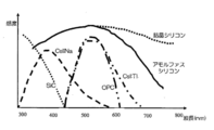
- a substrate having high resistance to radiation such as a SiC substrate is generally a wide cap (about 3 eV), and as an example, as shown in FIG. 19, the absorption edge is about 440 nm corresponding to the blue region. Therefore, in this case, a scintillator such as CsI: Tl or GOS that emits light in the green region cannot be used.
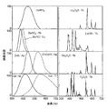
- FIG. 19 shows spectra of various materials when quinacridone is used as the organic photoelectric conversion material.
- the scintillator that emits light in these green regions has been actively researched due to the sensitivity characteristics of amorphous silicon, and therefore there is a high demand for using the scintillator.
- region can be used by comprising the photoelectric converting film 4 with the material containing the organic photoelectric conversion material which absorbs light emission in a green area
- the photoelectric conversion film 4 When the photoelectric conversion film 4 is formed of a material containing an organic photoelectric conversion material and the thin film transistor 10 is formed using a SiC substrate, the photoelectric conversion film 4 and the thin film transistor 10 have different sensitivity wavelength regions, and thus the light emitted by the scintillator is emitted. There is no noise of the thin film transistor 10.
- the photoelectric conversion film 4 in addition to receiving light emission mainly in the blue region, such as CsI: Na, light emission in the green region is also received. As a result, the sensitivity can be improved. In addition, since the organic photoelectric conversion material hardly absorbs radiation, it can be suitably used for the ISS system.
- SiC is highly resistant to radiation because it is difficult for nuclear nuclei to be blown away even when exposed to radiation.
- Develop semiconductor devices that can be used for a long time [online], [Search May 8, 2011], Internet ⁇ URL: http://www.jaea.go.jp/jari/jpn/publish/01/ff/ ff36 / sic.html> ”.
- C diamond
- BN diamond
- GaN gallium-nitride
- AlN gallium-nitride
- ZnO zinc-nitride
- These light element semiconductor materials have high radiation resistance because they are mainly wide-gap semiconductors, so they require high energy for ionization (electron-hole pair formation), small reaction cross-sections, This is due to the fact that bonding is strong and atomic displacement is less likely to occur.
- GaN has good thermal conductivity as a use other than blue LEDs and has high insulation resistance
- ICs are being studied in the field of power systems.
- ZnO an LED that emits light mainly in the blue to ultraviolet region has been studied.
- the band gap Eg is changed from about 1.1 eV to about 2.8 eV of Si, so that the light absorption wavelength ⁇ shifts to the short wavelength side.
- the wavelength ⁇ 1.24 / Eg ⁇ 1000
- the sensitivity changes to wavelengths up to about 440 nm. Therefore, when SiC is used, as shown in FIG. 20 as an example, the scintillator emits light in the blue region rather than CsI: Tl (peak wavelength: about 565 nm) that emits light in the green region, as well as CsI: Na (peak wavelength: about 420 nm). This is more suitable as the emission wavelength.
- CsI Na (peak wavelength: about 420 nm)
- BaFX Eu (X is a halogen such as Br and I, peak wavelength: about 380 nm)
- CaWO 4 peak wavelength: about 425 nm
- ZnS Ag (peak wavelength: about 450 nm)
- LaOBr Tb, Y 2 O 2 S: Tb, and the like
- BaFX Eu used in CsI: Na and CR cassettes
- CaWO 4 used in screens and films are preferably used.
- a CMOS sensor having high resistance to radiation may be configured by using a configuration of Si substrate / thick film SiO 2 / organic photoelectric conversion material by SOI (Silicon On Insulator).
- SOI Silicon On Insulator
- examples of the high radiation durability element include a complete separation type thick film SOI and a partial separation type thick film SOI.
- SOIs for example, “Patent Office,“ Patent Application Technology Trend Survey Report on SOI (Silicon On Insulator) Technology ”, [online], [Search May 8, 2011], Internet ⁇ URL: http://www.jpo.go.jp/shiryou/pdf/gidou-houkoku/soi.pdf> ”.
- the thin film transistor 10 or the like of the radiation detector 20 does not have light transmission (for example, a structure in which the active layer 17 is formed of a material having no light transmission such as amorphous silicon), the thin film transistor 10 or the like.
- a light-transmitting substrate 1 for example, a flexible substrate made of synthetic resin
- a portion of the substrate 1 where the thin film transistor 10 or the like is not formed is configured to transmit light. It is possible to obtain a radiation detector 20 having optical transparency.
- Arranging the thin film transistor 10 or the like having a non-light-transmitting structure on the light-transmitting substrate 1 is performed by separating the micro device block manufactured on the first substrate from the first substrate.
- FSA Fluid Self-Assembly
- the above FSA is, for example, “Toyama University,“ Study on Self-Aligned Placement Technology of Small Semiconductor Blocks ”, [online], [Search May 8, 2011], Internet ⁇ URL: http: //www3.u- toyama.ac.jp/maezawa/Research/FSA.html> ”.
Abstract
Provided are a radiological imaging device, program and radiological imaging method with which the irradiation state of radiation can be detected with high precision. When a first thin-film transistor (TFT) substrate is used to capture still images, the irradiation state of radiation is detected on the basis of charges read by a second TFT substrate provided for capturing video.
Description
本発明は、放射線画像撮影装置、プログラムおよび放射線画像撮影方法に関し、特に、被写体を透過した放射線により示される放射線画像を撮影する放射線画像撮影装置、プログラムおよび放射線画像撮影方法に関する。
The present invention relates to a radiographic image capturing apparatus, a program, and a radiographic image capturing method, and more particularly to a radiographic image capturing apparatus, a program, and a radiographic image capturing method for capturing a radiographic image indicated by radiation transmitted through a subject.
近年、TFT(Thin Film Transistor)アクティブマトリクス基板上に放射線感応層を配置し、X線等の放射線を直接デジタルデータに変換できるFPD(Flat Panel Detector)等の放射線検出器が実用化されている。この放射線検出器を用いた放射線画像撮影装置は、従来のX線フイルムやイメージングプレートを用いた放射線画像撮影装置に比べて、即時に画像を確認でき、連続的に放射線画像の撮影を行う透視撮影(動画撮影)も行うことができるといったメリットがある。
Recently, radiation detectors such as FPD (Flat Panel Detector) that can directly convert radiation such as X-rays into digital data by arranging a radiation sensitive layer on a TFT (Thin Film Transistor) active matrix substrate have been put into practical use. The radiographic imaging device using this radiation detector can see images immediately and can continuously capture radiographic images as compared with conventional radiographic imaging devices using X-ray film or imaging plate. There is an advantage that (moving image shooting) can also be performed.
この種の放射線検出器は、種々のタイプのものが提案されており、例えば、放射線を一度CsI:Tl、GOS(Gd2O2S:Tb)などのシンチレータで光に変換し、変換した光をフォトダイオードなどのセンサ部で電荷に変換して蓄積する間接変換方式がある。放射線画像撮影装置では、放射線検出器に蓄積された電荷を電気信号として読み出し、読み出した電気信号をアンプで増幅した後にA/D(アナログ/デジタル)変換部でデジタルデータに変換している。
Various types of radiation detectors of this type have been proposed. For example, radiation is once converted into light by a scintillator such as CsI: Tl, GOS (Gd 2 O 2 S: Tb), and converted light. There is an indirect conversion method in which a sensor unit such as a photodiode converts it into electric charge and stores it. In the radiographic imaging apparatus, the electric charge accumulated in the radiation detector is read as an electric signal, and the read electric signal is amplified by an amplifier and then converted into digital data by an A / D (analog / digital) converter.
ところで、この種の放射線画像撮影装置では、当該放射線画像撮影装置自身によって放射線の照射開始や照射停止、照射量等の照射状態を検出することができれば、放射線画像撮影装置および放射線源等を統括的に制御する撮影制御装置と放射線源との接続を行う必要がなくなるため、システム構成を簡略化したり、撮影制御装置による制御を簡略化したりするうえで好ましい。
By the way, in this type of radiographic imaging apparatus, if the radiographic imaging apparatus itself can detect the irradiation state such as the start and stop of irradiation and the irradiation amount, the radiographic imaging apparatus and the radiation source are integrated. Therefore, it is not necessary to connect the imaging control device to be controlled to the radiation source, which is preferable in simplifying the system configuration and simplifying the control by the imaging control device.
この種の放射線の照射状態を検出することのできる放射線画像撮影装置に関する技術として、特許第4217443号公報には、入射する放射線を可視光に変換する蛍光体と、前記可視光を電気信号に変換する第1の光電変換素子と該第1の光電変換素子からの電気信号の出力動作を切り換えるスイッチング素子とを含む画素を基板上に複数有してなる画素エリアを含み、前記第1の光電変換素子から出力される電気信号に基づいて画像情報が生成される放射線画像撮影装置であって、前記放射線の入射量を検出するための第2の光電変換素子を有し、前記スイッチング素子および前記第2の光電変換素子は、前記画素エリア内において前記基板と前記第1の光電変換素子との間に配置されていることを特徴とする放射線画像撮影装置が開示されている。
As a technique related to a radiographic imaging apparatus capable of detecting the irradiation state of this type of radiation, Japanese Patent No. 4217443 discloses a phosphor that converts incident radiation into visible light, and converts the visible light into an electrical signal. Including a pixel area including a plurality of pixels on a substrate including a first photoelectric conversion element that performs switching and a switching element that switches an output operation of an electric signal from the first photoelectric conversion element. A radiographic imaging apparatus in which image information is generated based on an electrical signal output from an element, comprising a second photoelectric conversion element for detecting an incident amount of the radiation, the switching element and the first The radiation image capturing apparatus is characterized in that the second photoelectric conversion element is disposed between the substrate and the first photoelectric conversion element in the pixel area. It is.
また、特許第4217506号公報には、第1の変換素子を有する画素を複数備える変換部を基板の放射線が入射する側に有し、前記変換部に入射した放射線量に応じて画像情報を出力する放射線撮像装置であって、前記変換部内に入射した放射線の照射量、前記変換部内への放射線の入射および放射線の停止のうち、少なくともいずれか1つを検出するための第2の変換素子を有し、前記第2の変換素子は、前記基板の放射線が入射する側で、前記変換部内の隣接する画素の前記第1の変換素子の間に、一方の幅が前記画素のピッチよりも小さい形状で配置されていることを特徴とする放射線撮像装置が開示されている。
Japanese Patent No. 4217506 has a conversion unit including a plurality of pixels each having a first conversion element on the side on which radiation of the substrate is incident, and outputs image information according to the amount of radiation incident on the conversion unit. A radiation imaging apparatus for detecting a second conversion element for detecting at least one of an irradiation amount of radiation incident in the conversion unit, incidence of radiation into the conversion unit, and stop of radiation. The second conversion element has a width smaller than the pitch of the pixels between the first conversion elements of adjacent pixels in the conversion unit on the side of the substrate on which radiation is incident. A radiation imaging apparatus characterized by being arranged in a shape is disclosed.
しかしながら、上記特許第4217443号および特許第4217506号に開示されている技術では、必ずしも放射線の照射状態を精度よく検出することができるとは限らない、という問題点があった。
However, the techniques disclosed in Japanese Patent Nos. 4217443 and 4217506 have a problem that the irradiation state of radiation cannot always be accurately detected.
すなわち、放射線画像の静止画像の撮影を行う場合には、被検者に対する被曝量を極力低減させるために、被検者の関心領域のみに絞って撮影を行う場合が多く、この場合、放射線の照射領域を関心領域のみとするように絞り込むコリメータが用いられる。
That is, when taking a still image of a radiographic image, in order to reduce the exposure dose to the subject as much as possible, imaging is often performed only on the region of interest of the subject. A collimator is used to narrow down the irradiation area to be only the area of interest.
この場合、上記特許第4217443号および特許第4217506号に開示されている技術では、放射線画像の撮影を行う放射線検出器に放射線の照射状態を検出するためのセンサが設けられているため、放射線の照射状態を検出するために用いることのできるセンサがコリメータによって絞られる結果、必ずしも高精度で放射線の照射状態を検出することができるとは限らないのである。
In this case, in the techniques disclosed in the above Patent Nos. 4217443 and 4217506, the radiation detector for capturing the radiation image is provided with a sensor for detecting the irradiation state of the radiation. As a result of a sensor that can be used to detect the irradiation state being narrowed by the collimator, it is not always possible to detect the irradiation state of radiation with high accuracy.
なお、このコリメータにより放射線の照射領域を絞る場合の問題は、放射線検出器のセンサ部に対して印加されるバイアス電圧の変化に応じて放射線の照射状態を検出する形態や、各画素からのリーク電流の変化に基づいて放射線の照射状態を検出する形態等においても生じ得る問題である。
Note that the problem of narrowing the radiation irradiation area with this collimator is that the radiation irradiation state is detected according to the change in the bias voltage applied to the sensor section of the radiation detector, and the leakage from each pixel. This is a problem that may occur even in the form of detecting the irradiation state of radiation based on a change in current.
また、放射線画像の撮影用の画素の一部を放射線の照射状態を検出するために用いる技術も考えられるが、この技術では、撮影によって得られた放射線画像に欠陥画素が生じることになるため、余り多くの画素を放射線の照射状態を検出するために用いることはできず、この技術においても、必ずしも高精度で放射線の照射状態を検出することができるとは限らない。
In addition, a technique that uses a part of the radiographic image capturing pixels to detect the irradiation state of the radiation is also conceivable. However, in this technique, defective pixels are generated in the radiographic image obtained by imaging. Too many pixels cannot be used for detecting the radiation irradiation state, and even with this technique, the radiation irradiation state cannot always be detected with high accuracy.
本発明は、上記問題点を解決するためになされたものであり、放射線の照射状態を高精度で検出することができる放射線画像撮影装置、プログラムおよび放射線画像撮影方法を提供することを目的とする。
The present invention has been made to solve the above-described problems, and an object of the present invention is to provide a radiographic image capturing apparatus, a program, and a radiographic image capturing method capable of detecting a radiation irradiation state with high accuracy. .
本発明の第1の態様に係る放射線画像撮影装置は、照射された放射線に応じた光を発生するか、または照射された放射線に応じた電荷を発生する放射線感応層、前記放射線感応層に積層され、当該放射線感応層が光を発生する場合に当該光に応じた電荷を発生する第1光電変換部および当該第1光電変換部により発生された電荷を読み出すための第1スイッチング素子を備えた複数の第1画素がマトリクス状に設けられるか、または前記放射線感応層が電荷を発生する場合に当該電荷を読み出すための第2スイッチング素子を備えた複数の第2画素がマトリクス状に設けられた静止画撮影用の第1基板、および前記放射線感応層の前記第1基板とは反対側の面に積層され、当該放射線感応層が光を発生する場合に当該光に応じた電荷を発生する第2光電変換部および当該第2光電変換部により発生された電荷を読み出すための第3スイッチング素子を備えた複数の第3画素がマトリクス状に設けられるか、または前記放射線感応層が電荷を発生する場合に当該電荷を読み出すための第4スイッチング素子を備えた複数の第4画素がマトリクス状に設けられた動画撮影用の第2基板を有する放射線検出器と、前記第1基板を用いて静止画撮影を行う場合、前記第2基板から読み出された電荷に基づいて放射線の照射状態を検出する検出手段と、前記検出手段による検出結果に基づいて、前記放射線検出器により静止画撮影を行うように制御する制御手段と、を備えている。
The radiographic imaging device according to the first aspect of the present invention includes a radiation-sensitive layer that generates light corresponding to irradiated radiation or generates a charge corresponding to irradiated radiation, and is laminated on the radiation-sensitive layer. A first photoelectric conversion unit that generates a charge corresponding to the light when the radiation sensitive layer generates light, and a first switching element for reading out the charge generated by the first photoelectric conversion unit. A plurality of first pixels are provided in a matrix, or a plurality of second pixels provided with a second switching element for reading out the charges when the radiation sensitive layer generates charges are provided in a matrix A first substrate for still image shooting and a layer opposite to the first substrate of the radiation sensitive layer are stacked, and when the radiation sensitive layer generates light, a charge corresponding to the light is generated. A plurality of third pixels having a second photoelectric conversion unit and a third switching element for reading out the electric charge generated by the second photoelectric conversion unit are provided in a matrix, or the radiation-sensitive layer has a charge. A radiation detector having a second substrate for moving image photography in which a plurality of fourth pixels each having a fourth switching element for reading out the electric charge when they are generated are provided in a matrix, and the first substrate. When still image shooting is performed, detection means for detecting the irradiation state of radiation based on the charges read from the second substrate, and still image shooting by the radiation detector based on the detection result by the detection means. Control means for controlling to perform.
第1の態様に係る放射線画像撮影装置によれば、放射線感応層に積層された静止画撮影用の第1基板を用いて静止画撮影が行われる一方、前記放射線感応層の前記第1基板とは反対側の面に積層された動画撮影用の第2基板を用いて動画撮影が行われる。
According to the radiographic imaging device according to the first aspect, still image shooting is performed using the first substrate for still image shooting laminated on the radiation sensitive layer, while the first substrate of the radiation sensitive layer is Moving image shooting is performed using the second substrate for moving image shooting stacked on the opposite surface.
ここで、本発明では、前記第1基板を用いて静止画撮影を行う場合、検出手段により、前記第2基板から読み出された電荷に基づいて放射線の照射状態が検出され、制御手段により、前記検出手段による検出結果に基づいて、前記放射線検出器により静止画撮影を行うように制御される。
Here, in the present invention, when taking a still image using the first substrate, the detection unit detects the irradiation state of the radiation based on the electric charge read from the second substrate, and the control unit Based on the detection result by the detection means, the radiation detector is controlled to perform still image shooting.
このように、第1の態様の放射線画像撮影装置によれば、第1基板を用いて静止画撮影を行う場合に、動画撮影用に設けられた第2基板から読み出された電荷に基づいて放射線の照射状態を検出しているので、第1基板を用いて検出する場合に比較して、放射線の照射状態を高精度で検出することができる。
Thus, according to the radiographic imaging device of the first aspect, when still image shooting is performed using the first substrate, based on the electric charges read from the second substrate provided for moving image shooting. Since the irradiation state of the radiation is detected, the irradiation state of the radiation can be detected with higher accuracy than when the detection is performed using the first substrate.
なお、本発明は、第2の態様として、前記第2基板を、前記第1基板に比較して低解像度および小サイズの少なくとも一方としてもよい。これにより、より高速に放射線の照射状態を検出することができる。
In the present invention, as the second aspect, the second substrate may have at least one of a low resolution and a small size as compared with the first substrate. Thereby, the irradiation state of radiation can be detected at higher speed.
また、本発明は、第3の態様として、前記第2基板が、前記放射線の照射状態を検出するための画素が放射線画像を撮影するための画素の間に設けられて構成されていてもよい。
In the present invention, as a third aspect, the second substrate may be configured such that pixels for detecting the radiation irradiation state are provided between pixels for capturing a radiation image. .
また、本発明は、第4の態様として、給電された状態で、前記第1基板から読み出された電荷に対して予め定められた信号処理を行う第1信号処理手段と、給電された状態で、前記第2基板から読み出された電荷に対して予め定められた信号処理を行う第2信号処理手段と、をさらに備え、前記制御手段が、前記検出手段によって前記放射線の照射開始を検出する場合、前記第1基板に対する給電を停止するように制御してもよい。これにより、消費電力を低減することができる。
According to a fourth aspect of the present invention, there is provided, as a fourth aspect, first signal processing means for performing predetermined signal processing on the electric charges read from the first substrate in a state where power is supplied, and a state where power is supplied And second signal processing means for performing predetermined signal processing on the charges read from the second substrate, and the control means detects the start of radiation irradiation by the detection means. In this case, the power supply to the first substrate may be stopped. Thereby, power consumption can be reduced.
また、本発明は、第5の態様として、前記第2基板から読み出された電荷を隣接する画素単位で合成するビニング状態および当該合成を行わない非ビニング状態を選択的に設定可能に構成されたビニング設定手段をさらに備え、前記制御手段が、前記検出手段によって前記放射線の照射開始を検出する場合、前記ビニング状態に設定するように前記ビニング設定手段を制御してもよい。これにより、より高速に放射線の照射状態を検出することができる。
As a fifth aspect of the present invention, a binning state in which charges read from the second substrate are combined in units of adjacent pixels and a non-binning state in which the combining is not performed can be selectively set. The binning setting unit may be further provided, and the control unit may control the binning setting unit to set the binning state when the detection unit detects the start of radiation irradiation. Thereby, the irradiation state of radiation can be detected at higher speed.
また、本発明は、第6の態様として、前記制御手段が、前記検出手段によって前記放射線の照射状態を検出する場合、前記第2基板からの電荷の読み出し速度を、動画撮影を行う場合より増加させるように制御してもよい。これにより、より高速に放射線の照射状態を検出することができる。
According to a sixth aspect of the present invention, as a sixth aspect, when the control means detects the radiation irradiation state by the detection means, the charge readout speed from the second substrate is increased as compared with the case of moving image shooting. You may control to make it. Thereby, the irradiation state of radiation can be detected at higher speed.
また、本発明は、第7の態様として、前記第1基板と前記第2基板との間、または前記第1基板の前記放射線感応層が積層されている面とは反対側の面、または前記第2基板の前記放射線感応層が積層されている面とは反対側の面に積層され、照射された放射線に応じた光を発生するか、または照射された放射線に応じた電荷を発生する第2放射線感応層をさらに備えてもよい。これにより、放射線の照射量も検出することができる。
In addition, the present invention provides, as a seventh aspect, a surface between the first substrate and the second substrate, a surface opposite to the surface on which the radiation sensitive layer of the first substrate is laminated, or the The second substrate is laminated on a surface opposite to the surface on which the radiation-sensitive layer is laminated, and generates light corresponding to the irradiated radiation or generates charges corresponding to the irradiated radiation. Two radiation sensitive layers may be further provided. Thereby, the radiation dose can also be detected.
特に、第7の態様は、第8の態様として、前記第2基板が、前記第2光電変換部として、各々光の検出感度が互いに異なる高感度光電変換部および低感度光電変換部を備え、前記検出手段が、前記第1基板を用いて静止画撮影を行う場合、前記高感度光電変換部によって得られた電荷に基づいて前記放射線の照射開始を検出し、前記低感度光電変換部によって得られた電荷に基づいて前記放射線の照射停止を検出してもよい。これにより、より高精度に放射線の照射状態を検出することができる。
In particular, in the seventh aspect, as the eighth aspect, the second substrate includes, as the second photoelectric conversion unit, a high-sensitivity photoelectric conversion unit and a low-sensitivity photoelectric conversion unit, each having different light detection sensitivities, When the detection means performs still image shooting using the first substrate, it detects the start of irradiation of the radiation based on the charge obtained by the high-sensitivity photoelectric conversion unit, and is obtained by the low-sensitivity photoelectric conversion unit. The irradiation stoppage of the radiation may be detected based on the generated electric charge. Thereby, the irradiation state of radiation can be detected with higher accuracy.
また、本発明は、第9の態様として、前記放射線検出器が、静止画像の撮影が行われる場合、前記第1基板が前記放射線感応層より放射線の入射される側に配置されるものとしてもよい。これにより、より高画質で静止画像の撮影を行うことができる。
Further, according to the ninth aspect of the present invention, as the ninth aspect, when the radiation detector is used to capture a still image, the first substrate may be disposed on the radiation incident side of the radiation sensitive layer. Good. As a result, still images can be taken with higher image quality.
さらに、本発明は、第10の態様として、前記放射線感応層が、照射された放射線に応じた光を発生する場合、柱状結晶を含んで構成されていてもよい。これにより、より高画質で静止画像の撮影を行うことができる。
Furthermore, in the present invention, as a tenth aspect, when the radiation sensitive layer generates light corresponding to the irradiated radiation, the radiation sensitive layer may include a columnar crystal. As a result, still images can be taken with higher image quality.
一方、上記目的を達成するために、本発明の第11の態様に係るプログラムは、コンピュータを、照射された放射線に応じた光を発生するか、または照射された放射線に応じた電荷を発生する放射線感応層、前記放射線感応層に積層され、当該放射線感応層が光を発生する場合に当該光に応じた電荷を発生する第1光電変換部および当該第1光電変換部により発生された電荷を読み出すための第1スイッチング素子を備えた複数の第1画素がマトリクス状に設けられるか、または前記放射線感応層が電荷を発生する場合に当該電荷を読み出すための第2スイッチング素子を備えた複数の第2画素がマトリクス状に設けられた静止画撮影用の第1基板、および前記放射線感応層の前記第1基板とは反対側の面に積層され、当該放射線感応層が光を発生する場合に当該光に応じた電荷を発生する第2光電変換部および当該第2光電変換部により発生された電荷を読み出すための第3スイッチング素子を備えた複数の第3画素がマトリクス状に設けられるか、または前記放射線感応層が電荷を発生する場合に当該電荷を読み出すための第4スイッチング素子を備えた複数の第4画素がマトリクス状に設けられた動画撮影用の第2基板を有する放射線検出器により、前記第1基板を用いて静止画撮影を行う場合、前記第2基板から読み出された電荷に基づいて放射線の照射状態を検出する検出手段と、前記検出手段による検出結果に基づいて、前記放射線検出器により静止画撮影を行うように制御する制御手段と、として機能させるためのものである。
On the other hand, in order to achieve the above object, the program according to the eleventh aspect of the present invention causes the computer to generate light corresponding to the irradiated radiation or generate a charge corresponding to the irradiated radiation. A radiation sensitive layer, laminated on the radiation sensitive layer, and when the radiation sensitive layer generates light, the first photoelectric conversion unit that generates a charge corresponding to the light and the charge generated by the first photoelectric conversion unit A plurality of first pixels having first switching elements for reading are provided in a matrix, or a plurality of second pixels having second switching elements for reading the charges when the radiation sensitive layer generates charges. A first substrate for photographing a still image in which second pixels are provided in a matrix, and a layer opposite to the first substrate of the radiation sensitive layer are stacked, and the radiation sensitive layer is A plurality of third pixels each having a second photoelectric conversion unit that generates a charge corresponding to the light and a third switching element for reading out the charge generated by the second photoelectric conversion unit. Or a second substrate for taking a moving image in which a plurality of fourth pixels provided with a fourth switching element for reading out the charge when the radiation sensitive layer generates a charge is provided in a matrix. When performing still image shooting using the first substrate by the radiation detector having, a detection means for detecting a radiation irradiation state based on the charge read from the second substrate, and a detection result by the detection means And a control means for controlling to take a still image by the radiation detector.
従って、第11の態様によれば、コンピュータを第1の態様に係る放射線画像撮影装置と同様に作用させることができるので、当該放射線画像撮影装置と同様に、放射線の照射状態を高精度で検出することができる。
Therefore, according to the eleventh aspect, since the computer can be operated in the same manner as the radiographic imaging apparatus according to the first aspect, the radiation irradiation state can be detected with high accuracy as in the radiographic imaging apparatus. can do.
さらに、上記目的を達成するために、第12の態様に係る放射線画像撮影方法は、照射された放射線に応じた光を発生するか、または照射された放射線に応じた電荷を発生する放射線感応層、前記放射線感応層に積層され、当該放射線感応層が光を発生する場合に当該光に応じた電荷を発生する第1光電変換部および当該第1光電変換部により発生された電荷を読み出すための第1スイッチング素子を備えた複数の第1画素がマトリクス状に設けられるか、または前記放射線感応層が電荷を発生する場合に当該電荷を読み出すための第2スイッチング素子を備えた複数の第2画素がマトリクス状に設けられた静止画撮影用の第1基板、および前記放射線感応層の前記第1基板とは反対側の面に積層され、当該放射線感応層が光を発生する場合に当該光に応じた電荷を発生する第2光電変換部および当該第2光電変換部により発生された電荷を読み出すための第3スイッチング素子を備えた複数の第3画素がマトリクス状に設けられるか、または前記放射線感応層が電荷を発生する場合に当該電荷を読み出すための第4スイッチング素子を備えた複数の第4画素がマトリクス状に設けられた動画撮影用の第2基板を有する放射線検出器により、前記第1基板を用いて静止画撮影を行う場合、前記第2基板から読み出された電荷に基づいて放射線の照射状態を検出する検出工程と、前記検出工程による検出結果に基づいて、前記放射線検出器により静止画撮影を行うように制御する制御工程と、を有している。
Furthermore, in order to achieve the above object, the radiographic imaging method according to the twelfth aspect generates a light corresponding to the irradiated radiation or generates a charge corresponding to the irradiated radiation. The first photoelectric conversion unit that is stacked on the radiation sensitive layer and generates a charge corresponding to the light when the radiation sensitive layer generates light, and for reading the charge generated by the first photoelectric conversion unit A plurality of first pixels provided with a first switching element are provided in a matrix or a plurality of second pixels provided with a second switching element for reading out the charge when the radiation sensitive layer generates a charge. Are stacked on a surface of the radiation sensitive layer opposite to the first substrate, and the radiation sensitive layer generates light. A plurality of third pixels having a second photoelectric conversion unit that generates a charge corresponding to the light and a third switching element for reading out the charge generated by the second photoelectric conversion unit in a matrix form Or a radiation detector having a second substrate for moving image photography in which a plurality of fourth pixels provided with a fourth switching element for reading out the charge when the radiation sensitive layer generates the charge are provided in a matrix. Thus, when performing still image shooting using the first substrate, based on the detection step of detecting the irradiation state of the radiation based on the charge read from the second substrate, and the detection result of the detection step, And a control step of controlling to take a still image by the radiation detector.
従って、第12の態様によれば、第1の態様に係る放射線画像撮影装置と同様に作用するので、当該放射線画像撮影装置と同様に、放射線の照射状態を高精度で検出することができる。
Therefore, according to the twelfth aspect, since it operates in the same manner as the radiographic image capturing apparatus according to the first aspect, it is possible to detect the radiation irradiation state with high accuracy as in the radiographic image capturing apparatus.
本発明によれば、第1基板を用いて静止画撮影を行う場合に、動画撮影用に設けられた第2基板から読み出された電荷に基づいて放射線の照射状態を検出しているので、第1基板を用いて検出する場合に比較して、放射線の照射状態を高精度で検出することができる、という効果を奏することができる。
According to the present invention, when still image shooting is performed using the first substrate, the radiation irradiation state is detected based on the electric charge read from the second substrate provided for moving image shooting. Compared with the case where detection is performed using the first substrate, an effect that the irradiation state of radiation can be detected with high accuracy can be achieved.
以下、図面を参照して、本発明を実施するための形態について詳細に説明する。
Hereinafter, embodiments for carrying out the present invention will be described in detail with reference to the drawings.
[第1の実施の形態]
まず、最初に本実施の形態に係る間接変換方式の放射線検出器20の構成について説明する。 [First Embodiment]
First, the configuration of the indirectconversion radiation detector 20 according to the present embodiment will be described.
まず、最初に本実施の形態に係る間接変換方式の放射線検出器20の構成について説明する。 [First Embodiment]
First, the configuration of the indirect
図1は、本発明の一実施の形態である放射線検出器20の3つの画素部分の構成を概略的に示す断面模式図である。
FIG. 1 is a schematic cross-sectional view schematically showing a configuration of three pixel portions of a radiation detector 20 according to an embodiment of the present invention.
この放射線検出器20は、絶縁性の基板1上に、信号出力部14、センサ部13、および透明絶縁膜7を順に形成することにより構成されたTFT基板30Aと、シンチレータ8と、接着層22と、TFT基板30Aと略同様の構成とされたTFT基板30Bと、がこの順に積層しており、TFT基板30AおよびTFT基板30Bの信号出力部14、センサ部13により画素部が構成されている。画素部は、基板1上に複数配列されており、各画素部における信号出力部14とセンサ部13とが重なりを有するように構成されている。
The radiation detector 20 includes a TFT substrate 30A configured by sequentially forming a signal output unit 14, a sensor unit 13, and a transparent insulating film 7 on an insulating substrate 1, a scintillator 8, and an adhesive layer 22. And a TFT substrate 30B having substantially the same configuration as the TFT substrate 30A are stacked in this order, and the pixel portion is configured by the TFT substrate 30A, the signal output unit 14 of the TFT substrate 30B, and the sensor unit 13. . A plurality of pixel units are arranged on the substrate 1, and the signal output unit 14 and the sensor unit 13 in each pixel unit are configured to overlap each other.
シンチレータ8は、センサ部13上に透明絶縁膜7を介して柱状結晶により形成されており、上方(TFT基板30B側)から入射してくる放射線を光に変換して発光する蛍光体を成膜したものである。このようなシンチレータ8を設けることで、被写体およびTFT基板30Bを透過した放射線を吸収して発光することになる。
The scintillator 8 is formed of a columnar crystal on the sensor unit 13 via the transparent insulating film 7, and forms a phosphor that emits light by converting radiation incident from above (TFT substrate 30 B side) into light. It is a thing. Providing such a scintillator 8 absorbs the radiation transmitted through the subject and the TFT substrate 30B and emits light.
シンチレータ8が発する光の波長域は、可視光域(波長360nm~830nm)であることが好ましく、この放射線検出器20によってモノクロ撮像を可能とするためには、緑色の波長域を含んでいることがより好ましい。
The wavelength range of light emitted by the scintillator 8 is preferably the visible light range (wavelength 360 nm to 830 nm), and in order to enable monochrome imaging by the radiation detector 20, the wavelength range of green is included. Is more preferable.
シンチレータ8に用いる蛍光体としては、具体的には、放射線としてX線を用いて撮像する場合、ヨウ化セシウム(CsI)を含むものが好ましく、X線照射時の発光スペクトルが、例えば、420nm~700nmにあるCsI:Tlを用いることが特に好ましい。なお、CsI:Tlの可視光域における発光ピーク波長は565nmである。
Specifically, the phosphor used in the scintillator 8 preferably contains cesium iodide (CsI) when imaging using X-rays as radiation, and the emission spectrum upon X-ray irradiation is, for example, 420 nm to It is particularly preferred to use CsI: Tl at 700 nm. Note that the emission peak wavelength in the visible light region of CsI: Tl is 565 nm.
また、本実施の形態では、一例として図2に示すように、シンチレータ8を、放射線入射側(TFT基板30B側)に柱状結晶71Aからなる柱状部が形成され、シンチレータ8の放射線入射側とは反対側に非柱状結晶71Bからなる非柱状部が形成された構成としており、シンチレータ8としてCsIを含む材料を用い、当該材料をTFT基板30Aに直接蒸着させることで、柱状部および非柱状部が形成されたシンチレータ8を得ている。なお、本実施の形態に係るシンチレータ8は、柱状結晶71Aの平均径が柱状結晶71Aの長手方向に沿っておよそ均一とされている。
In the present embodiment, as shown in FIG. 2 as an example, the scintillator 8 is formed with a columnar portion made of a columnar crystal 71A on the radiation incident side (TFT substrate 30B side). A non-columnar portion made of a non-columnar crystal 71B is formed on the opposite side. A material containing CsI is used as the scintillator 8, and the material is directly deposited on the TFT substrate 30A, so that the columnar portion and the non-columnar portion are formed. The formed scintillator 8 is obtained. In the scintillator 8 according to the present embodiment, the average diameter of the columnar crystals 71A is approximately uniform along the longitudinal direction of the columnar crystals 71A.
上記のように、シンチレータ8を柱状部が形成された構成にすることで、シンチレータ8で発生された光は柱状結晶71A内を進行し、非柱状結晶71Bを介してTFT基板30Aへ射出され、TFT基板30A側へ射出される光の拡散が抑制されることで、結果的に得られる放射線画像の鮮鋭度の低下が抑制される。また、シンチレータ8の柱状結晶71Aの先端部側に進行した光はTFT基板30Bに射出され、TFT基板30Bによる受光量の増加に寄与する。
As described above, by forming the scintillator 8 with the columnar portion, the light generated by the scintillator 8 travels in the columnar crystal 71A and is emitted to the TFT substrate 30A via the non-columnar crystal 71B. By suppressing the diffusion of the light emitted to the TFT substrate 30A side, a reduction in the sharpness of the resultant radiographic image is suppressed. Further, the light that has traveled toward the tip of the columnar crystal 71A of the scintillator 8 is emitted to the TFT substrate 30B, and contributes to an increase in the amount of light received by the TFT substrate 30B.
なお、非柱状部の空隙率を0(零)に近づけることにより、当該非柱状部による光の反射を抑制することができ、好ましい。また、非柱状部はできるだけ薄く(10μm程度)することが好ましい。
Note that it is preferable that the non-columnar portion has a porosity close to 0 (zero), whereby reflection of light by the non-columnar portion can be suppressed. Further, it is preferable to make the non-columnar portion as thin as possible (about 10 μm).
なお、本実施の形態では、シンチレータ8の放射線照射面側にTFT基板30Bが配置されているが、シンチレータ8とTFT基板30Bとをこのような位置関係で配置する方式は「表面読取方式(ISS:Irradiation Side Sampling)」と称する。シンチレータは放射線入射側がより強く発光するので、シンチレータの放射線入射側にTFT基板を配置する表面読取方式(ISS)は、シンチレータの放射線入射側とは反対側にTFT基板を配置する「裏面読取方式(PSS:Penetration Side Sampling)」よりもTFT基板とシンチレータの発光位置とが接近することから、撮影によって得られる放射線画像の分解能が高く、また、TFT基板の受光量が増大することで、結果として放射線画像の感度が向上する。
In the present embodiment, the TFT substrate 30B is disposed on the radiation irradiation surface side of the scintillator 8, but the method of disposing the scintillator 8 and the TFT substrate 30B in such a positional relationship is “surface reading method (ISS). : Irradiation Side Sampling) ”. Since the scintillator emits light more strongly on the radiation incident side, the surface reading method (ISS) in which the TFT substrate is disposed on the radiation incident side of the scintillator is the “back surface reading method (in which the TFT substrate is disposed on the opposite side of the scintillator from the radiation incident side” Since the TFT substrate and the light emission position of the scintillator are closer to each other than PSS (Penetration Side Sampling), the resolution of the radiographic image obtained by imaging is high, and the amount of light received by the TFT substrate is increased, resulting in radiation. Image sensitivity is improved.
一方、センサ部13は、上部電極6、下部電極2、および該上下の電極間に配置された光電変換膜4を有し、光電変換膜4は、シンチレータ8が発する光を吸収して電荷が発生する有機光電変換材料により構成されている。
On the other hand, the sensor unit 13 includes an upper electrode 6, a lower electrode 2, and a photoelectric conversion film 4 disposed between the upper and lower electrodes. The photoelectric conversion film 4 absorbs light emitted from the scintillator 8 and charges are generated. It is comprised with the organic photoelectric conversion material to generate | occur | produce.
上部電極6は、シンチレータにより生じた光を光電変換膜4に入射させる必要があるため、少なくともシンチレータの発光波長に対して透明な導電性材料で構成することが好ましく、具体的には、可視光に対する透過率が高く、抵抗値が小さい透明導電性酸化物(TCO;Transparent Conducting Oxide)を用いることが好ましい。なお、上部電極6としてAuなどの金属薄膜を用いることもできるが、透過率を90%以上得ようとすると抵抗値が増大し易いため、TCOの方が好ましい。例えば、ITO、IZO、AZO、FTO、SnO2、TiO2、ZnO2等を好ましく用いることができ、プロセス簡易性、低抵抗性、透明性の観点からはITOが最も好ましい。なお、上部電極6は、全画素部で共通の一枚構成としてもよく、画素部毎に分割してもよい。
The upper electrode 6 is preferably made of a conductive material transparent to at least the emission wavelength of the scintillator because it is necessary to make the light generated by the scintillator enter the photoelectric conversion film 4. It is preferable to use a transparent conductive oxide (TCO) having a high transmittance with respect to the surface and a low resistance value. Although a metal thin film such as Au can be used as the upper electrode 6, TCO is preferable because it tends to increase the resistance value when it is desired to obtain a transmittance of 90% or more. For example, ITO, IZO, AZO, FTO, SnO 2 , TiO 2 , ZnO 2 and the like can be preferably used, and ITO is most preferable from the viewpoint of process simplicity, low resistance, and transparency. Note that the upper electrode 6 may have a single configuration common to all the pixel portions, or may be divided for each pixel portion.
光電変換膜4は、有機光電変換材料を含み、シンチレータ8から発せられた光を吸収し、吸収した光に応じた電荷を発生する。このように有機光電変換材料を含む光電変換膜4であれば、可視域にシャープな吸収スペクトルを持ち、シンチレータ8による発光以外の電磁波が光電変換膜4に吸収されることがほとんどなく、X線等の放射線が光電変換膜4で吸収されることによって発生するノイズを効果的に抑制することができる。
The photoelectric conversion film 4 includes an organic photoelectric conversion material, absorbs light emitted from the scintillator 8, and generates electric charges according to the absorbed light. In this way, the photoelectric conversion film 4 containing an organic photoelectric conversion material has a sharp absorption spectrum in the visible range, and electromagnetic waves other than light emitted by the scintillator 8 are hardly absorbed by the photoelectric conversion film 4. The noise generated by the radiation such as being absorbed by the photoelectric conversion film 4 can be effectively suppressed.
光電変換膜4を構成する有機光電変換材料は、シンチレータ8で発光した光を最も効率よく吸収するために、その吸収ピーク波長が、シンチレータの発光ピーク波長と近いほど好ましい。有機光電変換材料の吸収ピーク波長とシンチレータの発光ピーク波長とが一致することが理想的であるが、双方の差が小さければシンチレータから発された光を十分に吸収することが可能である。具体的には、有機光電変換材料の吸収ピーク波長と、シンチレータの放射線に対する発光ピーク波長との差が、10nm以内であることが好ましく、5nm以内であることがより好ましい。
The organic photoelectric conversion material constituting the photoelectric conversion film 4 is preferably such that its absorption peak wavelength is closer to the emission peak wavelength of the scintillator in order to absorb light emitted by the scintillator 8 most efficiently. Ideally, the absorption peak wavelength of the organic photoelectric conversion material matches the emission peak wavelength of the scintillator, but if the difference between the two is small, the light emitted from the scintillator can be sufficiently absorbed. Specifically, the difference between the absorption peak wavelength of the organic photoelectric conversion material and the emission peak wavelength with respect to the radiation of the scintillator is preferably within 10 nm, and more preferably within 5 nm.
このような条件を満たすことが可能な有機光電変換材料としては、例えばキナクリドン系有機化合物およびフタロシアニン系有機化合物が挙げられる。例えばキナクリドンの可視域における吸収ピーク波長は560nmであるため、有機光電変換材料としてキナクリドンを用い、シンチレータ8の材料としてCsI:Tlを用いれば、上記ピーク波長の差を10nm以内にすることが可能となり、光電変換膜4で発生する電荷量をほぼ最大にすることができる。
Examples of the organic photoelectric conversion material that can satisfy such conditions include quinacridone organic compounds and phthalocyanine organic compounds. For example, since the absorption peak wavelength in the visible region of quinacridone is 560 nm, if quinacridone is used as the organic photoelectric conversion material and CsI: Tl is used as the material of the scintillator 8, the difference in peak wavelength can be made within 10 nm. The amount of charge generated in the photoelectric conversion film 4 can be substantially maximized.
次に、本実施の形態に係る放射線検出器20に適用可能な光電変換膜4について具体的に説明する。
Next, the photoelectric conversion film 4 applicable to the radiation detector 20 according to the present embodiment will be specifically described.
本実施の形態に係る放射線検出器20における電磁波吸収/光電変換部位は、1対の電極2,6と、該電極2,6間に挟まれた有機光電変換膜4を含む有機層により構成することができる。この有機層は、より具体的には、電磁波を吸収する部位、光電変換部位、電子輸送部位、正孔輸送部位、電子ブロッキング部位、正孔ブロッキング部位、結晶化防止部位、電極、および層間接触改良部位等の積み重ねもしくは混合により形成することができる。
The electromagnetic wave absorption / photoelectric conversion site in the radiation detector 20 according to the present embodiment is constituted by an organic layer including a pair of electrodes 2 and 6 and an organic photoelectric conversion film 4 sandwiched between the electrodes 2 and 6. be able to. More specifically, this organic layer is a part that absorbs electromagnetic waves, a photoelectric conversion part, an electron transport part, a hole transport part, an electron blocking part, a hole blocking part, a crystallization preventing part, an electrode, and an interlayer contact improvement. It can be formed by stacking or mixing parts.
上記有機層は、有機p型化合物または有機n型化合物を含有することが好ましい。
The organic layer preferably contains an organic p-type compound or an organic n-type compound.
有機p型半導体(化合物)は、主に正孔輸送性有機化合物に代表されるドナー性有機半導体(化合物)であり、電子を供与しやすい性質がある有機化合物をいう。さらに詳しくは2つの有機材料を接触させて用いたときにイオン化ポテンシャルの小さい方の有機化合物をいう。したがって、ドナー性有機化合物としては、電子供与性のある有機化合物であればいずれの有機化合物も使用可能である。
An organic p-type semiconductor (compound) is a donor organic semiconductor (compound) typified by a hole-transporting organic compound and refers to an organic compound having a property of easily donating electrons. More specifically, an organic compound having a smaller ionization potential when two organic materials are used in contact with each other. Therefore, any organic compound can be used as the donor organic compound as long as it is an electron-donating organic compound.
有機n型半導体(化合物)は、主に電子輸送性有機化合物に代表されるアクセプター性有機半導体(化合物)であり、電子を受容しやすい性質がある有機化合物をいう。さらに詳しくは2つの有機化合物を接触させて用いたときに電子親和力の大きい方の有機化合物をいう。したがって、アクセプター性有機化合物は、電子受容性のある有機化合物であればいずれの有機化合物も使用可能である。
An organic n-type semiconductor (compound) is an acceptor organic semiconductor (compound) typified by an electron-transporting organic compound and refers to an organic compound having a property of easily accepting electrons. More specifically, the organic compound having the higher electron affinity when two organic compounds are used in contact with each other. Therefore, as the acceptor organic compound, any organic compound can be used as long as it is an electron-accepting organic compound.
この有機p型半導体および有機n型半導体として適用可能な材料、および光電変換膜4の構成については、特開2009-32854号公報において詳細に説明されているため説明を省略する。
The materials applicable as the organic p-type semiconductor and the organic n-type semiconductor, and the configuration of the photoelectric conversion film 4 are described in detail in Japanese Patent Application Laid-Open No. 2009-32854, and thus the description thereof is omitted.
光電変換膜4の厚みは、シンチレータ8からの光を吸収する点では膜厚は大きいほど好ましいが、ある程度以上厚くなると光電変換膜4の両端から印加されるバイアス電圧により光電変換膜4に発生する電界の強度が低下して電荷が収集できなくなるため、30nm以上300nm以下が好ましく、より好ましくは、50nm以上250nm以下、特に好ましくは80nm以上200nm以下である。
The thickness of the photoelectric conversion film 4 is preferably as large as possible in terms of absorbing light from the scintillator 8. However, when the thickness is more than a certain level, the photoelectric conversion film 4 is generated in the photoelectric conversion film 4 by a bias voltage applied from both ends of the photoelectric conversion film 4. Since electric field strength is reduced and charges cannot be collected, the thickness is preferably 30 nm to 300 nm, more preferably 50 nm to 250 nm, and particularly preferably 80 nm to 200 nm.
なお、図1に示す放射線検出器20では、光電変換膜4は、全画素部で共通の一枚構成であるが、画素部毎に分割してもよい。
In the radiation detector 20 shown in FIG. 1, the photoelectric conversion film 4 has a single-sheet configuration common to all the pixel portions, but may be divided for each pixel portion.
下部電極2は、画素部毎に分割された薄膜とする。下部電極2は、透明又は不透明の導電性材料で構成することができ、アルミニウム、銀等を好適に用いることができる。
The lower electrode 2 is a thin film divided for each pixel portion. The lower electrode 2 can be made of a transparent or opaque conductive material, and aluminum, silver, or the like can be suitably used.
下部電極2の厚みは、例えば、30nm以上300nm以下とすることができる。
The thickness of the lower electrode 2 can be, for example, 30 nm or more and 300 nm or less.
センサ部13では、上部電極6と下部電極2の間に所定のバイアス電圧を印加することで、光電変換膜4で発生した電荷(正孔、電子)のうちの一方を上部電極6に移動させ、他方を下部電極2に移動させることができる。本実施の形態の放射線検出器20では、上部電極6に配線が接続され、この配線を介してバイアス電圧が上部電極6に印加されるものとする。また、バイアス電圧は、光電変換膜4で発生した電子が上部電極6に移動し、正孔が下部電極2に移動するように極性が決められているものとするが、この極性は逆であってもよい。
In the sensor unit 13, by applying a predetermined bias voltage between the upper electrode 6 and the lower electrode 2, one of electric charges (holes, electrons) generated in the photoelectric conversion film 4 is moved to the upper electrode 6. The other can be moved to the lower electrode 2. In the radiation detector 20 of the present embodiment, a wiring is connected to the upper electrode 6, and a bias voltage is applied to the upper electrode 6 through this wiring. In addition, the polarity of the bias voltage is determined so that electrons generated in the photoelectric conversion film 4 move to the upper electrode 6 and holes move to the lower electrode 2, but this polarity is reversed. May be.
各画素部を構成するセンサ部13は、少なくとも下部電極2、光電変換膜4、および上部電極6を含んでいればよいが、暗電流の増加を抑制するため、電子ブロッキング膜3および正孔ブロッキング膜5の少なくともいずれかを設けることが好ましく、両方を設けることがより好ましい。
The sensor unit 13 constituting each pixel unit only needs to include at least the lower electrode 2, the photoelectric conversion film 4, and the upper electrode 6. In order to suppress an increase in dark current, the electron blocking film 3 and hole blocking are performed. It is preferable to provide at least one of the films 5, and it is more preferable to provide both.
電子ブロッキング膜3は、下部電極2と光電変換膜4との間に設けることができ、下部電極2と上部電極6間にバイアス電圧を印加したときに、下部電極2から光電変換膜4に電子が注入されて暗電流が増加してしまうのを抑制することができる。
The electron blocking film 3 can be provided between the lower electrode 2 and the photoelectric conversion film 4. When a bias voltage is applied between the lower electrode 2 and the upper electrode 6, electrons are transferred from the lower electrode 2 to the photoelectric conversion film 4. It is possible to suppress the dark current from increasing due to the injection of.
電子ブロッキング膜3には、電子供与性有機材料を用いることができる。
An electron donating organic material can be used for the electron blocking film 3.
実際に電子ブロッキング膜3に用いる材料は、隣接する電極の材料および隣接する光電変換膜4の材料等に応じて選択すればよく、隣接する電極の材料の仕事関数(Wf)より1.3eV以上電子親和力(Ea)が大きく、かつ、隣接する光電変換膜4の材料のイオン化ポテンシャル(Ip)と同等のIpもしくはそれより小さいIpを持つものが好ましい。この電子供与性有機材料として適用可能な材料については、特開2009-32854号公報において詳細に説明されているため説明を省略する。なお、光電変換膜4は、さらにフラーレン若しくはカーボンナノチューブを含有させて形成してもよい。
The material actually used for the electron blocking film 3 may be selected according to the material of the adjacent electrode, the material of the adjacent photoelectric conversion film 4 and the like, and 1.3 eV or more from the work function (Wf) of the material of the adjacent electrode. Those having a large electron affinity (Ea) and an Ip equivalent to or smaller than the ionization potential (Ip) of the material of the adjacent photoelectric conversion film 4 are preferable. Since the material applicable as the electron donating organic material is described in detail in Japanese Patent Application Laid-Open No. 2009-32854, description thereof is omitted. The photoelectric conversion film 4 may be formed by further containing fullerenes or carbon nanotubes.
電子ブロッキング膜3の厚みは、暗電流抑制効果を確実に発揮させるとともに、センサ部13の光電変換効率の低下を防ぐため、10nm以上200nm以下が好ましく、さらに好ましくは30nm以上150nm以下、特に好ましくは50nm以上100nm以下である。
The thickness of the electron blocking film 3 is preferably 10 nm or more and 200 nm or less, more preferably 30 nm or more and 150 nm or less, and particularly preferably, in order to surely exhibit the dark current suppressing effect and prevent a decrease in photoelectric conversion efficiency of the sensor unit 13. It is 50 nm or more and 100 nm or less.
正孔ブロッキング膜5は、光電変換膜4と上部電極6との間に設けることができ、下部電極2と上部電極6間にバイアス電圧を印加したときに、上部電極6から光電変換膜4に正孔が注入されて暗電流が増加してしまうのを抑制することができる。
The hole blocking film 5 can be provided between the photoelectric conversion film 4 and the upper electrode 6. When a bias voltage is applied between the lower electrode 2 and the upper electrode 6, the hole blocking film 5 is transferred from the upper electrode 6 to the photoelectric conversion film 4. It is possible to suppress the increase in dark current due to the injection of holes.
正孔ブロッキング膜5には、電子受容性有機材料を用いることができる。
An electron-accepting organic material can be used for the hole blocking film 5.
正孔ブロッキング膜5の厚みは、暗電流抑制効果を確実に発揮させるとともに、センサ部13の光電変換効率の低下を防ぐため、10nm以上200nm以下が好ましく、さらに好ましくは30nm以上150nm以下、特に好ましくは50nm以上100nm以下である。
The thickness of the hole blocking film 5 is preferably 10 nm or more and 200 nm or less, more preferably 30 nm or more and 150 nm or less, and particularly preferably, in order to surely exhibit the dark current suppressing effect and prevent a decrease in photoelectric conversion efficiency of the sensor unit 13. Is from 50 nm to 100 nm.
実際に正孔ブロッキング膜5に用いる材料は、隣接する電極の材料および隣接する光電変換膜4の材料等に応じて選択すればよく、隣接する電極の材料の仕事関数(Wf)より1.3eV以上イオン化ポテンシャル(Ip)が大きく、かつ、隣接する光電変換膜4の材料の電子親和力(Ea)と同等のEaもしくはそれより大きいEaを持つものが好ましい。この電子受容性有機材料として適用可能な材料については、特開2009-32854号公報において詳細に説明されているため説明を省略する。
The material actually used for the hole blocking film 5 may be selected according to the material of the adjacent electrode, the material of the adjacent photoelectric conversion film 4 and the like, and 1.3 eV from the work function (Wf) of the material of the adjacent electrode. As described above, it is preferable that the ionization potential (Ip) is large and that the Ea is equal to or larger than the electron affinity (Ea) of the material of the adjacent photoelectric conversion film 4. Since the material applicable as the electron-accepting organic material is described in detail in Japanese Patent Application Laid-Open No. 2009-32854, description thereof is omitted.
なお、光電変換膜4で発生した電荷のうち、正孔が上部電極6に移動し、電子が下部電極2に移動するようにバイアス電圧を設定する場合には、電子ブロッキング膜3と正孔ブロッキング膜5の位置を逆にすればよい。また、電子ブロッキング膜3と正孔ブロッキング膜5は両方設けなくてもよく、いずれかを設けておけば、ある程度の暗電流抑制効果を得ることができる。
In addition, when a bias voltage is set so that holes move to the upper electrode 6 and electrons move to the lower electrode 2 among the charges generated in the photoelectric conversion film 4, the electron blocking film 3 and the hole blocking are set. The position of the film 5 may be reversed. Moreover, it is not necessary to provide both the electron blocking film 3 and the hole blocking film 5. If either one is provided, a certain degree of dark current suppressing effect can be obtained.
各画素部の下部電極2下方の基板1の表面には信号出力部14が形成されている。
A signal output unit 14 is formed on the surface of the substrate 1 below the lower electrode 2 of each pixel unit.
図3には、信号出力部14の構成が概略的に示されている。
FIG. 3 schematically shows the configuration of the signal output unit 14.
下部電極2に対応して、下部電極2に移動した電荷を蓄積するコンデンサ9と、コンデンサ9に蓄積された電荷を電気信号に変換して出力する電界効果型薄膜トランジスタ(Thin Film Transistor、以下、単に「薄膜トランジスタ」という。)10が形成されている。コンデンサ9および薄膜トランジスタ10の形成された領域は、平面視において下部電極2と重なる部分を有しており、このような構成とすることで、各画素部における信号出力部14とセンサ部13とが厚さ方向で重なりを有することとなる。なお、放射線検出器20(画素部)の平面積を最小にするために、コンデンサ9および薄膜トランジスタ10の形成された領域が下部電極2によって完全に覆われていることが望ましい。
Corresponding to the lower electrode 2, a capacitor 9 that accumulates the charges transferred to the lower electrode 2, and a field effect thin film transistor (Thin Transistor, hereinafter simply referred to as an electric signal converted from the electric charge accumulated in the capacitor 9) "Thin film transistor") 10 is formed. The region in which the capacitor 9 and the thin film transistor 10 are formed has a portion that overlaps the lower electrode 2 in a plan view. With such a configuration, the signal output unit 14 and the sensor unit 13 in each pixel unit are connected to each other. There will be overlap in the thickness direction. In order to minimize the plane area of the radiation detector 20 (pixel portion), it is desirable that the region where the capacitor 9 and the thin film transistor 10 are formed is completely covered by the lower electrode 2.
コンデンサ9は、基板1と下部電極2との間に設けられた絶縁膜11を貫通して形成された導電性材料の配線を介して対応する下部電極2と電気的に接続されている。これにより、下部電極2で捕集された電荷をコンデンサ9に移動させることができる。
The capacitor 9 is electrically connected to the corresponding lower electrode 2 via a wiring made of a conductive material penetrating an insulating film 11 provided between the substrate 1 and the lower electrode 2. Thereby, the electric charge collected by the lower electrode 2 can be moved to the capacitor 9.
薄膜トランジスタ10は、ゲート電極15、ゲート絶縁膜16、および活性層(チャネル層)17が積層され、さらに、活性層17上にソース電極18とドレイン電極19が所定の間隔を開けて形成されている。
In the thin film transistor 10, a gate electrode 15, a gate insulating film 16, and an active layer (channel layer) 17 are stacked, and a source electrode 18 and a drain electrode 19 are formed on the active layer 17 at a predetermined interval. .
活性層17は、例えば、アモルファスシリコンや非晶質酸化物、有機半導体材料、カーボンナノチューブなどにより形成することができる。なお、活性層17を構成する材料は、これらに限定されるものではない。
The active layer 17 can be formed of, for example, amorphous silicon, amorphous oxide, organic semiconductor material, carbon nanotube, or the like. In addition, the material which comprises the active layer 17 is not limited to these.
活性層17を構成可能な非晶質酸化物としては、In、GaおよびZnのうちの少なくとも1つを含む酸化物(例えばIn-O系)が好ましく、In、GaおよびZnのうちの少なくとも2つを含む酸化物(例えばIn-Zn-O系、In-Ga-O系、Ga-Zn-O系)がより好ましく、In、GaおよびZnを含む酸化物が特に好ましい。In-Ga-Zn-O系非晶質酸化物としては、結晶状態における組成がInGaO3(ZnO)m(mは6未満の自然数)で表される非晶質酸化物が好ましく、特に、InGaZnO4がより好ましい。なお、活性層17を構成可能な非晶質酸化物は、これらに限定されるものではない。
The amorphous oxide that can form the active layer 17 is preferably an oxide containing at least one of In, Ga, and Zn (for example, In—O-based), and at least 2 of In, Ga, and Zn. (Eg, In—Zn—O, In—Ga—O, and Ga—Zn—O) are more preferable, and oxides including In, Ga, and Zn are particularly preferable. As the In—Ga—Zn—O-based amorphous oxide, an amorphous oxide whose composition in a crystalline state is represented by InGaO 3 (ZnO) m (m is a natural number of less than 6) is preferable, and InGaZnO is particularly preferable. 4 is more preferable. In addition, the amorphous oxide which can comprise the active layer 17 is not limited to these.
活性層17を構成可能な有機半導体材料としては、フタロシアニン化合物や、ペンタセン、バナジルフタロシアニン等を挙げることができるが、これらに限定されるものではない。なお、フタロシアニン化合物の構成については、特開2009-212389号公報において詳細に説明されているため説明を省略する。
Examples of the organic semiconductor material that can form the active layer 17 include, but are not limited to, phthalocyanine compounds, pentacene, vanadyl phthalocyanine, and the like. Note that the configuration of the phthalocyanine compound is described in detail in JP-A-2009-212389, and thus the description thereof is omitted.
薄膜トランジスタ10の活性層17を非晶質酸化物や有機半導体材料、カーボンナノチューブで形成したものとすれば、X線等の放射線を吸収せず、あるいは吸収したとしても極めて微量に留まるため、信号出力部14におけるノイズの発生を効果的に抑制することができる。
If the active layer 17 of the thin film transistor 10 is formed of an amorphous oxide, an organic semiconductor material, or a carbon nanotube, it will not absorb radiation such as X-rays, or even if it absorbs it, it will remain in a very small amount. Generation of noise in the portion 14 can be effectively suppressed.
また、活性層17をカーボンナノチューブで形成した場合、薄膜トランジスタ10のスイッチング速度を高速化することができ、また、可視光域での光の吸収度合の低い薄膜トランジスタ10を形成できる。なお、カーボンナノチューブで活性層17を形成する場合、活性層17に極微量の金属性不純物が混入するだけで、薄膜トランジスタ10の性能は著しく低下するため、遠心分離などにより極めて高純度のカーボンナノチューブを分離・抽出して形成する必要がある。
Further, when the active layer 17 is formed of carbon nanotubes, the switching speed of the thin film transistor 10 can be increased, and the thin film transistor 10 having a low degree of light absorption in the visible light region can be formed. Note that when the active layer 17 is formed of carbon nanotubes, the performance of the thin film transistor 10 is remarkably deteriorated only by mixing a very small amount of metallic impurities into the active layer 17. It is necessary to form by separating and extracting.
ここで、上述した非晶質酸化物、有機半導体材料、カーボンナノチューブや、有機光電変換材料は、いずれも低温での成膜が可能である。従って、基板1としては、半導体基板、石英基板、およびガラス基板等の耐熱性の高い基板に限定されず、プラスチック等の可撓性基板、アラミド、バイオナノファイバを用いることもできる。具体的には、ポリエチレンテレフタレート、ポリブチレンフタレート、ポリエチレンナフタレート等のポリエステル、ポリスチレン、ポリカーボネート、ポリエーテルスルホン、ポリアリレート、ポリイミド、ポリシクロオレフィン、ノルボルネン樹脂、ポリ(クロロトリフルオロエチレン)等の可撓性基板を用いることができる。このようなプラスチック製の可撓性基板を用いれば、軽量化を図ることもでき、例えば持ち運び等に有利となる。
Here, any of the above-described amorphous oxide, organic semiconductor material, carbon nanotube, and organic photoelectric conversion material can be formed at a low temperature. Therefore, the substrate 1 is not limited to a substrate having high heat resistance such as a semiconductor substrate, a quartz substrate, and a glass substrate, and a flexible substrate such as plastic, aramid, or bio-nanofiber can also be used. Specifically, flexible materials such as polyesters such as polyethylene terephthalate, polybutylene phthalate, and polyethylene naphthalate, polystyrene, polycarbonate, polyethersulfone, polyarylate, polyimide, polycycloolefin, norbornene resin, and poly (chlorotrifluoroethylene). A conductive substrate can be used. If such a plastic flexible substrate is used, it is possible to reduce the weight, which is advantageous for carrying around, for example.
また、基板1には、絶縁性を確保するための絶縁層、水分や酸素の透過を防止するためのガスバリア層、平坦性あるいは電極等との密着性を向上するためのアンダーコート層等を設けてもよい。
In addition, the substrate 1 is provided with an insulating layer for ensuring insulation, a gas barrier layer for preventing permeation of moisture and oxygen, an undercoat layer for improving flatness or adhesion to electrodes, and the like. May be.
アラミドは、200度以上の高温プロセスを適用できるために,透明電極材料を高温硬化させて低抵抗化でき、また、ハンダのリフロー工程を含むドライバICの自動実装にも対応できる。また、アラミドは、ITO(indium tin oxide)やガラス基板と熱膨張係数が近いため、製造後の反りが少なく、割れにくい。また、アラミドは、ガラス基板等と比べて薄く基板を形成できる。なお、超薄型ガラス基板とアラミドを積層して基板1を形成してもよい。
Since aramid can be applied to a high temperature process of 200 degrees or more, the transparent electrode material can be cured at a high temperature to reduce the resistance, and it can also be used for automatic mounting of a driver IC including a solder reflow process. Moreover, since aramid has a thermal expansion coefficient close to that of ITO (indium tin oxide) or a glass substrate, warping after production is small and it is difficult to crack. In addition, aramid can form a substrate thinner than a glass substrate or the like. The substrate 1 may be formed by laminating an ultrathin glass substrate and aramid.
バイオナノファイバは、バクテリア(酢酸菌、Acetobacter Xylinum)が産出するセルロースミクロフィブリル束(バクテリアセルロース)と透明樹脂との複合したものである。セルロースミクロフィブリル束は、幅50nmと可視光波長に対して1/10のサイズで、かつ、高強度、高弾性、低熱膨である。バクテリアセルロースにアクリル樹脂、エポキシ樹脂等の透明樹脂を含浸・硬化させることで、繊維を60-70%も含有しながら、波長500nmで約90%の光透過率を示すバイオナノファイバが得られる。バイオナノファイバは、シリコン結晶に匹敵する低い熱膨張係数(3-7ppm)を有し、鋼鉄並の強度(460MPa)、高弾性(30GPa)で、かつフレキシブルであることから、ガラス基板等と比べて薄く基板1を形成できる。
Bionanofiber is a composite of cellulose microfibril bundle (bacterial cellulose) produced by bacteria (acetic acid bacteria, Acetobacter® Xylinum) and transparent resin. The cellulose microfibril bundle has a width of 50 nm and a size of 1/10 of the visible light wavelength, and has high strength, high elasticity, and low thermal expansion. By impregnating and curing a transparent resin such as acrylic resin or epoxy resin into bacterial cellulose, a bio-nanofiber having a light transmittance of about 90% at a wavelength of 500 nm can be obtained while containing 60-70% of the fiber. Bionanofiber has a low coefficient of thermal expansion (3-7ppm) comparable to silicon crystals, and is as strong as steel (460MPa), highly elastic (30GPa), and flexible. Compared to glass substrates, etc. The substrate 1 can be formed thinly.
本実施の形態に係るTFT基板30Bの構成は、TFT基板30Aと略同様であるが、図4に模式的に示すように、TFT基板30Aがシンチレータ8よりも一回りサイズが小さいのに対して、TFT基板30Bはシンチレータ8と略同一のサイズとされている点、およびTFT基板30BはTFT基板30Aより画素密度が高い(解像度が高い)ものとして構成されている点がTFT基板30Aとは異なっている。なお、この形態に限らず、これらの2点の何れか一方のみの相違とされていてもよい。
The configuration of the TFT substrate 30B according to the present embodiment is substantially the same as that of the TFT substrate 30A, but the TFT substrate 30A is slightly smaller in size than the scintillator 8 as schematically shown in FIG. The TFT substrate 30B is different from the TFT substrate 30A in that the TFT substrate 30B has substantially the same size as the scintillator 8, and the TFT substrate 30B is configured to have a higher pixel density (higher resolution) than the TFT substrate 30A. ing. In addition, it is not restricted to this form, You may be considered as the difference only in any one of these two points.
なお、前述したように、本実施の形態に係る放射線検出器20では、シンチレータ8をTFT基板30A上に直接蒸着により形成する一方、シンチレータ8のTFT基板30Aが設けられている面とは反対側の面にTFT基板30Bを、接着層22を介して接着することにより構成しているが、これに限らず、例えば、シンチレータ8をTFT基板30B上に直接蒸着により形成する一方、シンチレータ8のTFT基板30Bが設けられている面とは反対側の面にTFT基板30Aを、接着層22を介して接着することにより構成する方法等、他の方法により構成してもよいことは言うまでもない。
As described above, in the radiation detector 20 according to the present embodiment, the scintillator 8 is formed directly on the TFT substrate 30A by vapor deposition, while the side of the scintillator 8 opposite to the surface on which the TFT substrate 30A is provided. The TFT substrate 30B is bonded to the surface of the TFT substrate 30 via the adhesive layer 22. However, the present invention is not limited to this. For example, the scintillator 8 is formed directly on the TFT substrate 30B by vapor deposition. It goes without saying that the TFT substrate 30A may be formed by other methods such as a method of bonding the TFT substrate 30A to the surface opposite to the surface on which the substrate 30B is provided via the adhesive layer 22.
また、本実施の形態に係る放射線検出器20では、シンチレータ8の各柱状部の先端部は、できるだけ平坦になるように制御することが好ましい。具体的には、蒸着終了時の被蒸着基板の温度を制御することで実現できる。例えば、蒸着終了時の被蒸着基板の温度を110℃とすれば先端角度がおよそ170度となり、蒸着終了時の被蒸着基板の温度を140℃とすれば先端角度がおよそ60度となり、蒸着終了時の被蒸着基板の温度を200℃とすれば先端角度がおよそ70度となり、蒸着終了時の被蒸着基板の温度を260℃とすれば先端角度がおよそ120度となる。なお、この制御については、特開2010-25620号公報において詳細に説明されているため、これ以上の説明を省略する。
Also, in the radiation detector 20 according to the present embodiment, it is preferable to control the tip of each columnar part of the scintillator 8 to be as flat as possible. Specifically, it can be realized by controlling the temperature of the evaporation target substrate at the end of evaporation. For example, if the temperature of the substrate to be deposited at the end of vapor deposition is 110 ° C., the tip angle is about 170 degrees, and if the temperature of the substrate to be deposited at the end of vapor deposition is 140 degrees Celsius, the tip angle is about 60 degrees. If the temperature of the vapor deposition substrate at that time is 200 ° C., the tip angle is approximately 70 degrees, and if the temperature of the vapor deposition substrate at the end of vapor deposition is 260 ° C., the tip angle is approximately 120 degrees. Since this control is described in detail in Japanese Patent Application Laid-Open No. 2010-25620, further description is omitted.
一方、TFT基板30AおよびTFT基板30Bには、図5に示すように、上述のセンサ部13、コンデンサ9、薄膜トランジスタ10を含んで構成される画素32が一定方向(図5の行方向)および当該一定方向に対する交差方向(図5の列方向)に2次元状に複数設けられている。
On the other hand, on the TFT substrate 30A and the TFT substrate 30B, as shown in FIG. 5, the pixels 32 including the sensor unit 13, the capacitor 9, and the thin film transistor 10 are arranged in a certain direction (row direction in FIG. 5) and A plurality of two-dimensional shapes are provided in a crossing direction (column direction in FIG. 5) with respect to a certain direction.
また、放射線検出器20には、上記一定方向(走査線方向)に延設され、各薄膜トランジスタ10をオン・オフさせるための複数本のゲート配線34と、上記交差方向(信号配線方向)に延設され、オン状態の薄膜トランジスタ10を介して電荷を読み出すための複数本のデータ配線36と、が各々TFT基板30AおよびTFT基板30Bに対応して2組分設けられている。
In addition, the radiation detector 20 extends in the predetermined direction (scanning line direction), and extends in the intersecting direction (signal wiring direction) with a plurality of gate wirings 34 for turning on and off each thin film transistor 10. A plurality of data wirings 36 for reading out charges through the thin film transistor 10 in the on state are provided in two sets corresponding to the TFT substrate 30A and the TFT substrate 30B, respectively.
放射線検出器20は、平板状で平面視において外縁に4辺を有する四辺形状をしている。具体的には矩形状に形成されている。
The radiation detector 20 is flat and has a quadrilateral shape with four sides at the outer edge in plan view. Specifically, it is formed in a rectangular shape.
次に、この放射線検出器20を内蔵し、放射線画像を撮影する可搬型の放射線画像撮影装置(以下、「電子カセッテ」という。)40の構成について説明する。図6には、本実施の形態に係る電子カセッテ40の構成を示す斜視図が示されている。
Next, the configuration of a portable radiation image capturing apparatus (hereinafter referred to as “electronic cassette”) 40 that incorporates the radiation detector 20 and captures a radiation image will be described. FIG. 6 is a perspective view showing the configuration of the electronic cassette 40 according to the present exemplary embodiment.
同図に示すように、この電子カセッテ40は、放射線を透過させる材料からなる平板状の筐体41を備えており、防水性、密閉性を有する構造とされている。筐体41の内部には、放射線Xが照射される筐体41の照射面側から、被写体を透過した放射線Xを検出する放射線検出器20、および放射線Xのバック散乱線を吸収する鉛板43が順に配設される。筐体41は、平板状の一方の面の放射線検出器20の配設位置に対応する領域が放射線を検出可能な四辺形状の撮影領域41Aとされている。放射線検出器20は、図7に示すように、TFT基板30Bが撮影領域41A側となるように配置されており、撮影領域41Aを構成する筐体41内側に貼り付けられている。
As shown in the figure, the electronic cassette 40 includes a flat housing 41 made of a material that transmits radiation, and has a waterproof and airtight structure. Inside the housing 41 are a radiation detector 20 that detects the radiation X that has passed through the subject from the irradiation surface side of the housing 41 that is irradiated with the radiation X, and a lead plate 43 that absorbs backscattered rays of the radiation X. Are arranged in order. The case 41 has a quadrilateral imaging region 41A capable of detecting radiation in a region corresponding to the arrangement position of the radiation detector 20 on one flat surface. As shown in FIG. 7, the radiation detector 20 is disposed so that the TFT substrate 30B is on the imaging region 41A side, and is affixed to the inside of the housing 41 constituting the imaging region 41A.
また、筐体41の内部の一端側には、放射線検出器20と重ならない位置(撮影領域41Aの範囲外)に、後述するカセッテ制御部58や電源部70を収容するケース42が配置されている。
In addition, a case 42 that accommodates a cassette control unit 58 and a power supply unit 70 described later is disposed on one end side inside the housing 41 at a position that does not overlap the radiation detector 20 (outside the range of the imaging region 41A). Yes.
図8には、本実施の形態に係る電子カセッテ40の電気系の要部構成を示すブロック図が示されている。
FIG. 8 is a block diagram showing the main configuration of the electrical system of the electronic cassette 40 according to the present embodiment.
TFT基板30A、30Bは、それぞれ隣り合う2辺の一辺側にゲート線ドライバ52が配置され、他辺側に信号処理部54が配置されている。以下、2つのTFT基板30A、30Bに対応して設けられたゲート線ドライバ52および信号処理部54を区別する場合、TFT基板30Aに対応するゲート線ドライバ52および信号処理部54に符号Aを付し、TFT基板30Bに対応するゲート線ドライバ52および信号処理部54に符号Bを付して説明する。
In the TFT substrates 30A and 30B, a gate line driver 52 is disposed on one side of two adjacent sides, and a signal processing unit 54 is disposed on the other side. Hereinafter, when the gate line driver 52 and the signal processing unit 54 provided corresponding to the two TFT substrates 30A and 30B are distinguished from each other, the gate line driver 52 and the signal processing unit 54 corresponding to the TFT substrate 30A are denoted by A. The gate line driver 52 and the signal processing unit 54 corresponding to the TFT substrate 30B will be described with reference character B.
TFT基板30Aの個々のゲート配線34はゲート線ドライバ52Aに接続され、TFT基板30Aの個々のデータ配線36は信号処理部54Aに接続されており、TFT基板30Bの個々のゲート配線34はゲート線ドライバ52Bに接続されており、TFT基板30Bの個々のデータ配線36は信号処理部54Bに接続されている。
Each gate wiring 34 of the TFT substrate 30A is connected to the gate line driver 52A, each data wiring 36 of the TFT substrate 30A is connected to the signal processing unit 54A, and each gate wiring 34 of the TFT substrate 30B is a gate line. Connected to the driver 52B, each data wiring 36 of the TFT substrate 30B is connected to the signal processing unit 54B.
また、筐体41の内部には、画像メモリ56と、カセッテ制御部58と、無線通信部60とを備えている。
In addition, the housing 41 includes an image memory 56, a cassette control unit 58, and a wireless communication unit 60.
TFT基板30A、30Bの各薄膜トランジスタ10は、ゲート線ドライバ52A、52Bからゲート配線34を介して供給される信号により走査線単位で順にオンされ、オン状態とされた薄膜トランジスタ10によって読み出された電荷は、電気信号としてデータ配線36を伝送されて信号処理部54A、54Bに入力される。これにより、電荷は走査線単位で順に読み出され、二次元状の放射線画像が取得可能となる。
The thin film transistors 10 on the TFT substrates 30A and 30B are sequentially turned on in units of scanning lines by signals supplied from the gate line drivers 52A and 52B via the gate wiring 34, and the electric charges read by the thin film transistors 10 turned on. Is transmitted through the data wiring 36 as an electrical signal and input to the signal processing units 54A and 54B. As a result, the charges are sequentially read in units of scanning lines, and a two-dimensional radiation image can be acquired.
ここで、本実施の形態に係る信号処理部54Aおよび信号処理部54Bの構成について説明する。図9には、本実施の形態に係る信号処理部54Bの構成を示す回路図が示されている。
Here, the configuration of the signal processing unit 54A and the signal processing unit 54B according to the present embodiment will be described. FIG. 9 is a circuit diagram showing the configuration of the signal processing unit 54B according to the present embodiment.
同図に示すように、本実施の形態に係る信号処理部54Bは、TFT基板30Bのデータ配線36の各々に対応して、可変ゲインプリアンプ(チャージアンプ)82と、サンプルホールド回路86と、が備えられている。
As shown in the figure, the signal processing unit 54B according to the present embodiment includes a variable gain preamplifier (charge amplifier) 82 and a sample hold circuit 86 corresponding to each of the data wirings 36 on the TFT substrate 30B. Is provided.
可変ゲインプリアンプ82は、正入力側が接地されたオペアンプ82Aと、オペアンプ82Aの負入力側と出力側との間に、それぞれ並列に接続されるコンデンサ82Bと、リセットスイッチ82Cとを含んで構成されており、リセットスイッチ82Cは、カセッテ制御部58により切り換えられる。
The variable gain preamplifier 82 includes an operational amplifier 82A whose positive input side is grounded, a capacitor 82B connected in parallel between the negative input side and the output side of the operational amplifier 82A, and a reset switch 82C. The reset switch 82C is switched by the cassette control unit 58.
また、本実施の形態に係る信号処理部54Bは、マルチプレクサ88およびA/D(アナログ/デジタル)変換器89が備えられている。なお、サンプルホールド回路86のサンプルタイミング、およびマルチプレクサ88に設けられたスイッチ88Aによる選択出力も、カセッテ制御部58により切り換えられる。
Further, the signal processing unit 54B according to the present embodiment includes a multiplexer 88 and an A / D (analog / digital) converter 89. Note that the sample control of the sample hold circuit 86 and the selection output by the switch 88A provided in the multiplexer 88 are also switched by the cassette control unit 58.
放射線画像を検出する際に、カセッテ制御部58は、まず、可変ゲインプリアンプ82のリセットスイッチ82Cを所定期間オン状態とすることにより、コンデンサ82Bに蓄積されていた電荷を放電する。
When detecting the radiation image, the cassette control unit 58 first discharges the charge accumulated in the capacitor 82B by turning on the reset switch 82C of the variable gain preamplifier 82 for a predetermined period.
一方、放射線Xが照射されることによってTFT基板30Bの各画素32の各々のコンデンサ9に蓄積された電荷は、接続されている薄膜トランジスタ10がオン状態とされることにより電気信号として接続されているデータ配線36を伝送され、データ配線36を伝送された電気信号は、対応する可変ゲインプリアンプ82により、予め定められた増幅率で増幅される。
On the other hand, the electric charge accumulated in each capacitor 9 of each pixel 32 of the TFT substrate 30B by being irradiated with the radiation X is connected as an electric signal when the connected thin film transistor 10 is turned on. The electric signal transmitted through the data line 36 and transmitted through the data line 36 is amplified by a corresponding variable gain preamplifier 82 at a predetermined amplification factor.
一方、カセッテ制御部58は、上述した放電を行った後、サンプルホールド回路86を所定期間駆動させることより、可変ゲインプリアンプ82によって増幅された電気信号の信号レベルをサンプルホールド回路86に保持させる。
On the other hand, the cassette control unit 58 causes the sample hold circuit 86 to hold the signal level of the electric signal amplified by the variable gain preamplifier 82 by driving the sample hold circuit 86 for a predetermined period after performing the above-described discharge.
そして、各サンプルホールド回路86に保持された信号レベルは、カセッテ制御部58による制御に応じてマルチプレクサ88により順次選択され、A/D変換器89によってA/D変換されることにより、撮影された放射線画像を示す画像データが生成される。
The signal levels held in each sample and hold circuit 86 are sequentially selected by the multiplexer 88 in accordance with control by the cassette control unit 58 and are A / D converted by the A / D converter 89 and photographed. Image data indicating a radiation image is generated.
一方、信号処理部54Bには画像メモリ56が接続されており、信号処理部54BのA/D変換器89から出力された画像データは画像メモリ56に順に記憶される。画像メモリ56は所定枚分の画像データを記憶可能な記憶容量を有しており、放射線画像の撮影が行われる毎に、撮影によって得られた画像データが画像メモリ56に順次記憶される。
On the other hand, an image memory 56 is connected to the signal processing unit 54B, and the image data output from the A / D converter 89 of the signal processing unit 54B is stored in the image memory 56 in order. The image memory 56 has a storage capacity capable of storing a predetermined number of image data, and image data obtained by imaging is sequentially stored in the image memory 56 each time a radiographic image is captured.
一方、図10には、本実施の形態に係る信号処理部54Aの構成を示す回路図が示されている。
On the other hand, FIG. 10 shows a circuit diagram showing a configuration of the signal processing unit 54A according to the present embodiment.
同図に示すように、本実施の形態に係る信号処理部54Aは、TFT基板30Aのデータ配線36の各々に対応して、可変ゲインプリアンプ(チャージアンプ)92と、ビニング部94と、サンプルホールド回路96と、が備えられている。
As shown in the figure, the signal processing unit 54A according to the present embodiment corresponds to each of the data wirings 36 on the TFT substrate 30A, and includes a variable gain preamplifier (charge amplifier) 92, a binning unit 94, and a sample hold. Circuit 96 is provided.
可変ゲインプリアンプ92は、正入力側が接地されたオペアンプ92Aと、オペアンプ92Aの負入力側と出力側との間に、それぞれ並列に接続されるコンデンサ92Bと、リセットスイッチ92Cとを含んで構成されており、リセットスイッチ92Cは、カセッテ制御部58により切り換えられる。
The variable gain preamplifier 92 includes an operational amplifier 92A whose positive input side is grounded, a capacitor 92B connected in parallel between the negative input side and the output side of the operational amplifier 92A, and a reset switch 92C. The reset switch 92C is switched by the cassette control unit 58.
また、ビニング部94は、隣り合う通信線間に接続されるスイッチ94Aと、通信線の途中に接続されるスイッチ94B,94Cとを含んで構成され、各スイッチ94A,94B,94Cも、カセッテ制御部58により切り換えられる。本実施の形態では、スイッチ94Aおよびスイッチ94Bをオン状態にすると共に、スイッチ94Cをオフ状態にすることによりビニング接続状態とされ、スイッチ94Bおよびスイッチ94Cをオン状態にすると共に、スイッチ94Aをオフ状態にすることにより通常接続状態とされる。
The binning unit 94 includes a switch 94A connected between adjacent communication lines and switches 94B and 94C connected in the middle of the communication lines, and each of the switches 94A, 94B and 94C is also cassette-controlled. Switching is performed by the unit 58. In the present embodiment, the switch 94A and the switch 94B are turned on and the switch 94C is turned off to be in the binning connection state. The switch 94B and the switch 94C are turned on and the switch 94A is turned off. By doing so, a normal connection state is established.
また、本実施の形態に係る信号処理部54Aは、マルチプレクサ98およびA/D変換器99が備えられている。なお、サンプルホールド回路96のサンプルタイミング、およびマルチプレクサ98に設けられたスイッチ98Aによる選択出力も、カセッテ制御部58により切り換えられる。
The signal processing unit 54A according to the present embodiment includes a multiplexer 98 and an A / D converter 99. Note that the sample control of the sample hold circuit 96 and the selection output by the switch 98A provided in the multiplexer 98 are also switched by the cassette control unit 58.
TFT基板30Aのデータ配線36の各々は、可変ゲインプリアンプ92、ビニング部94、およびサンプルホールド回路96を順に介してマルチプレクサ98の入力端に各々個別に接続される。そして、マルチプレクサ98の出力端は、出力端が画像メモリ56に接続されたA/D変換器99の入力端に接続されている。
Each of the data wirings 36 of the TFT substrate 30A is individually connected to the input terminal of the multiplexer 98 through the variable gain preamplifier 92, the binning unit 94, and the sample hold circuit 96 in order. The output terminal of the multiplexer 98 is connected to the input terminal of the A / D converter 99 whose output terminal is connected to the image memory 56.
放射線画像を検出する際に、カセッテ制御部58は、まず、可変ゲインプリアンプ92のリセットスイッチ92Cを所定期間オン状態とすることにより、コンデンサ92Bに蓄積されていた電荷を放電(リセット)する。
When detecting the radiation image, the cassette control unit 58 first discharges (resets) the charge accumulated in the capacitor 92B by turning on the reset switch 92C of the variable gain preamplifier 92 for a predetermined period.
次に、カセッテ制御部58は、可変ゲインプリアンプ92のリセットスイッチ92Cをオフ状態にすると共に、ビニング部94のスイッチ94A~94Cのオン/オフ状態の設定によってビニング接続状態または通常接続状態に設定する。
Next, the cassette control unit 58 turns off the reset switch 92C of the variable gain preamplifier 92 and sets the binning connection state or the normal connection state by setting the on / off states of the switches 94A to 94C of the binning unit 94. .
一方、放射線Xが照射されることによってTFT基板30Aの画素32の各々のコンデンサ9に蓄積された電荷は、接続されている薄膜トランジスタ10がオン状態とされることにより電気信号として接続されているデータ配線36を伝送され、データ配線36を伝送された電気信号は、対応する可変ゲインプリアンプ92により、予め定められた増幅率で増幅された後に、ビニング部94によって必要に応じて合成される。
On the other hand, the charge accumulated in each capacitor 9 of the pixel 32 of the TFT substrate 30A by the irradiation with the radiation X is the data connected as an electrical signal when the connected thin film transistor 10 is turned on. The electrical signal transmitted through the wiring 36 and transmitted through the data wiring 36 is amplified by a corresponding variable gain preamplifier 92 at a predetermined amplification factor, and then synthesized by the binning unit 94 as necessary.
一方、カセッテ制御部58は、上述したコンデンサ92Bの放電およびビニング部94の設定を行った後、サンプルホールド回路96を所定期間駆動させることより、可変ゲインプリアンプ92によって増幅され、必要に応じてビニング(合成)された電気信号の信号レベルをサンプルホールド回路96に保持させる。
On the other hand, after the discharge of the capacitor 92B and the setting of the binning unit 94 are performed, the cassette control unit 58 is amplified by the variable gain preamplifier 92 by driving the sample hold circuit 96 for a predetermined period, and binning is performed as necessary. The signal level of the (synthesized) electric signal is held in the sample hold circuit 96.
そして、各サンプルホールド回路96に保持された信号レベルは、カセッテ制御部58による制御に応じてマルチプレクサ98により順次選択され、A/D変換器99によってA/D変換されることにより、撮影された放射線画像を示す画像データが生成される。
The signal levels held in the sample and hold circuits 96 are sequentially selected by the multiplexer 98 in accordance with the control by the cassette control unit 58 and are A / D converted by the A / D converter 99 to be photographed. Image data indicating a radiation image is generated.
一方、信号処理部54Aには画像メモリ56が接続されており、信号処理部54AのA/D変換器99から出力された画像データは画像メモリ56に順に記憶される。画像メモリ56は所定枚分の画像データを記憶可能な記憶容量を有しており、放射線画像の撮影が行われる毎に、撮影によって得られた画像データが画像メモリ56に順次記憶される。
On the other hand, an image memory 56 is connected to the signal processing unit 54A, and the image data output from the A / D converter 99 of the signal processing unit 54A is stored in the image memory 56 in order. The image memory 56 has a storage capacity capable of storing a predetermined number of image data, and image data obtained by imaging is sequentially stored in the image memory 56 each time a radiographic image is captured.
画像メモリ56はカセッテ制御部58と接続されている。カセッテ制御部58はマイクロコンピュータによって構成され、CPU(中央処理装置)58A、ROM(Read Only Memory)およびRAM(Random Access Memory)を含むメモリ58B、フラッシュメモリ等からなる不揮発性の記憶部58Cを備えており、電子カセッテ40全体の動作を制御する。
The image memory 56 is connected to the cassette control unit 58. The cassette control unit 58 is constituted by a microcomputer, and includes a CPU (Central Processing Unit) 58A, a memory 58B including a ROM (Read Only Memory) and a RAM (Random Access Memory), a non-volatile storage unit 58C including a flash memory and the like. The operation of the entire electronic cassette 40 is controlled.
また、カセッテ制御部58には無線通信部60が接続されている。無線通信部60は、IEEE(Institute of Electrical and Electronics Engineers)802.11a/b/g/n等に代表される無線LAN(Local Area Network)規格に対応しており、無線通信による外部機器との間での各種情報の伝送を制御する。カセッテ制御部58は、無線通信部60を介して、放射線撮影全体を制御するコンソールなどの外部装置と無線通信が可能とされており、コンソールとの間で各種情報の送受信が可能とされている。
Also, a wireless communication unit 60 is connected to the cassette control unit 58. The wireless communication unit 60 corresponds to a wireless LAN (Local Area Network) standard represented by IEEE (Institute of Electrical and Electronics Electronics) (802.11a / b / g / n), etc., and communicates with an external device by wireless communication. Control the transmission of various information between them. The cassette control unit 58 can wirelessly communicate with an external device such as a console for controlling the entire radiation imaging via the wireless communication unit 60, and can transmit and receive various types of information to and from the console. .
また、電子カセッテ40には、電源部70が設けられており、上述した各種回路や各素子(ゲート線ドライバ52A、52B、信号処理部54A、54B、画像メモリ56、無線通信部60やカセッテ制御部58として機能するマイクロコンピュータ等)は、電源部70から供給された電力によって作動する。電源部70は、電子カセッテ40の可搬性を損なわないように、バッテリ(充電可能な二次電池)を内蔵しており、充電されたバッテリから各種回路・素子へ電力を供給する。なお、図8では、電源部70と各種回路や各素子を接続する配線を省略している。
In addition, the electronic cassette 40 is provided with a power supply unit 70, and the various circuits and elements described above ( gate line drivers 52A and 52B, signal processing units 54A and 54B, image memory 56, wireless communication unit 60, and cassette control). The microcomputer functioning as the unit 58 is operated by the electric power supplied from the power supply unit 70. The power supply unit 70 incorporates a battery (a rechargeable secondary battery) so as not to impair the portability of the electronic cassette 40, and supplies power from the charged battery to various circuits and elements. In FIG. 8, wiring for connecting the power supply unit 70 to various circuits and elements is omitted.
なお、本実施の形態に係る電子カセッテ40では、電源部70から信号処理部54Aへの給電および給電停止と、電源部70から信号処理部54Bへの給電および給電停止とを、カセッテ制御部58により各々個別に切り替えることができるものとされている。
Note that in the electronic cassette 40 according to the present exemplary embodiment, the cassette control unit 58 performs power supply and power supply stop from the power supply unit 70 to the signal processing unit 54A and power supply and power supply stop from the power supply unit 70 to the signal processing unit 54B. Can be switched individually.
ところで、本実施の形態に係る電子カセッテ40は、静止画像の撮影と動画像の撮影の双方を行うことができるものとして構成されている。ここで、本実施の形態に係る電子カセッテ40では、TFT基板30Aが動画像の撮影用の基板として用いられ、TFT基板30Bが静止画像の撮影用の基板として用いられる。
By the way, the electronic cassette 40 according to the present embodiment is configured to be able to perform both still image shooting and moving image shooting. Here, in the electronic cassette 40 according to the present exemplary embodiment, the TFT substrate 30A is used as a moving image shooting substrate, and the TFT substrate 30B is used as a still image shooting substrate.
そして、本実施の形態に係る電子カセッテ40は、放射線画像の撮影を行う場合、撮影領域41Aを上とし、図7に示すように、放射線を発生する放射線発生装置80と間隔を空けて配置され、撮影領域上に患者の撮影対象部位Bが配置される。放射線発生装置80は予め与えられた撮影条件等に応じた放射線量の放射線Xを射出する。放射線発生装置80から射出された放射線Xは、撮影対象部位Bを透過することで画像情報を担持した後に電子カセッテ40に照射される。
When radiographic images are captured, the electronic cassette 40 according to the present embodiment is arranged with the imaging region 41A facing upward and spaced apart from the radiation generator 80 that generates radiation, as shown in FIG. The imaging target region B of the patient is arranged on the imaging area. The radiation generator 80 emits radiation X having a radiation dose according to imaging conditions given in advance. The radiation X emitted from the radiation generator 80 is irradiated to the electronic cassette 40 after carrying image information by passing through the imaging target region B.
放射線発生装置80から照射された放射線Xは、撮影対象部位Bを透過した後に電子カセッテ40に到達する。これにより、電子カセッテ40に内蔵された放射線検出器20の各センサ部13には照射された放射線Xの線量に応じた電荷が発生し、コンデンサ9にはセンサ部13で発生した電荷が蓄積される。
The radiation X emitted from the radiation generator 80 reaches the electronic cassette 40 after passing through the imaging target region B. As a result, charges corresponding to the dose of the irradiated radiation X are generated in each sensor unit 13 of the radiation detector 20 incorporated in the electronic cassette 40, and the charges generated by the sensor unit 13 are accumulated in the capacitor 9. The
一方、カセッテ制御部58は、静止画像の撮影を行う場合には、ゲート線ドライバ52Bを制御し、ゲート線ドライバ52BからTFT基板30Bの各ゲート配線34に1ラインずつ順にオン信号を出力させて画像情報の読み出しを行う。これにより、放射線検出器20のTFT基板30Bから読み出された画像情報は、信号処理部54Bを経た後に画像データ(以下、「静止画像データ」という。)として画像メモリ56に記憶されるので、カセッテ制御部58は、当該静止画像データを画像メモリ56から読み出し、無線通信部60を介してコンソールに送信する。コンソールは、受信した静止画像データを予め定められた記憶装置に記憶すると共に、当該画像データにより示される静止画をディスプレイ装置により表示させる。
On the other hand, the cassette control unit 58 controls the gate line driver 52B when shooting a still image, and sequentially outputs an ON signal line by line from the gate line driver 52B to each gate wiring 34 of the TFT substrate 30B. Read image information. Accordingly, the image information read from the TFT substrate 30B of the radiation detector 20 is stored in the image memory 56 as image data (hereinafter referred to as “still image data”) after passing through the signal processing unit 54B. The cassette control unit 58 reads the still image data from the image memory 56 and transmits it to the console via the wireless communication unit 60. The console stores the received still image data in a predetermined storage device and causes the display device to display a still image indicated by the image data.
これに対し、カセッテ制御部58は、動画像の撮影を行う場合には、ゲート線ドライバ52Aを制御し、ゲート線ドライバ52AからTFT基板30Aの各ゲート配線34に1ラインずつ順にオン信号を出力させて画像情報の読み出しを行うことを、予め定められたフレームレート(本実施の形態では、30フレーム/秒)に応じた速度で繰り返し実行する。これにより、放射線検出器20のTFT基板30Aから読み出された画像情報は、信号処理部54Aを経た後に画像データ(以下、「動画像データ」という。)として画像メモリ56に順次記憶されるので、カセッテ制御部58は、当該動画像データを画像メモリ56から連続的に読み出し、無線通信部60を介してコンソールにリアルタイムで送信する。コンソールは、電子カセッテ40から受信した動画像データにより示される動画像をディスプレイ装置によってリアルタイムで表示することにより、動画像(透視画像)の表示を行う。
On the other hand, the cassette control unit 58 controls the gate line driver 52A when shooting a moving image, and sequentially outputs an ON signal line by line from the gate line driver 52A to each gate wiring 34 of the TFT substrate 30A. Then, the reading of the image information is repeatedly executed at a speed corresponding to a predetermined frame rate (30 frames / second in the present embodiment). Thus, the image information read from the TFT substrate 30A of the radiation detector 20 is sequentially stored in the image memory 56 as image data (hereinafter referred to as “moving image data”) after passing through the signal processing unit 54A. The cassette control unit 58 continuously reads out the moving image data from the image memory 56 and transmits the moving image data to the console via the wireless communication unit 60 in real time. The console displays a moving image (perspective image) by displaying the moving image indicated by the moving image data received from the electronic cassette 40 in real time on the display device.
なお、本実施の形態に係る電子カセッテ40では、TFT基板30Bから読み出された静止画像データとTFT基板30Aから読み出された動画像データとを、各々画像メモリ56の異なる記憶領域に記憶するものとされている。
In the electronic cassette 40 according to the present embodiment, still image data read from the TFT substrate 30B and moving image data read from the TFT substrate 30A are stored in different storage areas of the image memory 56, respectively. It is supposed to be.
ところで、本実施の形態に係る電子カセッテ40には、静止画像の撮影を行う際に、TFT基板30Aから読み出された情報に基づいて放射線の照射開始を検出し、当該照射開始を検出した時点で放射線画像の撮影を行う同期フリー機能が搭載されている。
By the way, in the electronic cassette 40 according to the present exemplary embodiment, when a still image is captured, the start of radiation irradiation is detected based on information read from the TFT substrate 30A, and the start of the irradiation is detected. It is equipped with a synchronization-free function that captures radiographic images.
次に、図11を参照して、同期フリー機能を働かせる場合の本実施の形態に係る電子カセッテ40の作用について詳細に説明する。なお、図11は、この際に電子カセッテ40のカセッテ制御部58におけるCPU58Aにより実行される静止画撮影処理プログラムの処理の流れを示すフローチャートであり、当該プログラムはメモリ58BのROMに予め記憶されている。
Next, with reference to FIG. 11, the operation of the electronic cassette 40 according to the present exemplary embodiment when the synchronization free function is activated will be described in detail. FIG. 11 is a flowchart showing a flow of processing of a still image shooting processing program executed by the CPU 58A in the cassette control unit 58 of the electronic cassette 40 at this time, and the program is stored in advance in the ROM of the memory 58B. Yes.
同図のステップ100では、カセッテ制御部58は、電源部70から信号処理部54Aへの給電を開始させるように制御し、次のステップ102では、信号処理部54Aのビニング部94をビニング接続状態となるように制御する。
In step 100 of the figure, the cassette control unit 58 performs control so as to start power supply from the power supply unit 70 to the signal processing unit 54A, and in the next step 102, the binning unit 94 of the signal processing unit 54A is in the binning connection state. Control to be
次のステップ104では、カセッテ制御部58は、ゲート線ドライバ52Aを制御して、ゲート線ドライバ52Aから各ゲート配線34に1ラインずつ順にオン信号を出力させ、TFT基板30Aの各画素32におけるコンデンサ9に蓄積された電荷を放電させることにより、TFT基板30Aの各画素32をリセットすると共に、TFT基板30Aからの電荷の読み出し速度(フレームレート)を、動画撮影を行う場合より増加させるように制御する。なお、本ステップ104の処理によって行われる各画素32のリセット動作は1回のみでもよく、複数回繰り返してもよい。
In the next step 104, the cassette control unit 58 controls the gate line driver 52A to sequentially output an ON signal line by line from the gate line driver 52A to each gate wiring 34, and the capacitor in each pixel 32 of the TFT substrate 30A. 9, by resetting the pixels 32 of the TFT substrate 30A by discharging the charges accumulated in the TFT 9, the charge reading speed (frame rate) from the TFT substrate 30A is controlled to be higher than that for moving image shooting. To do. Note that the reset operation of each pixel 32 performed by the process of step 104 may be performed only once or may be repeated a plurality of times.
次のステップ105では、カセッテ制御部58は、前述した動画撮影時の動作を開始させる。これにより、画像メモリ56には、動画像データが順次記憶される。
In the next step 105, the cassette control unit 58 starts the above-described operation during moving image shooting. Thereby, the moving image data is sequentially stored in the image memory 56.
そこで、次のステップ106では、カセッテ制御部58は、信号処理部54Aから画像メモリ56に記憶された動画像データを読み出し、当該動画像データに基づいて、照射されている放射線Xの線量(以下、「放射線量」という。)を導出し、次のステップ108にて、導出した放射線量が予め定められた閾値に達したか否かを判定することにより、放射線の照射が開始されたか否かを判定して、否定判定となった場合は上記ステップ106に戻る一方、肯定判定となった時点でステップ109に移行する。なお、本実施の形態では、上記ステップ106による放射線量の導出を、信号処理部54Aから画像メモリ56に記憶された動画像データにおける全ての画素値を合算することにより行っている。しかし、これに限らず、当該動画像データにおける一部の画素値を合算することにより導出する形態や、当該動画像データにおける少なくとも一部の画素値の平均値を算出することにより導出する形態等としてもよい。
Therefore, in the next step 106, the cassette control unit 58 reads out the moving image data stored in the image memory 56 from the signal processing unit 54A, and based on the moving image data, the radiation X-ray dose (hereinafter referred to as irradiation dose). In the next step 108, it is determined whether or not radiation irradiation has been started by determining whether or not the derived radiation dose has reached a predetermined threshold value. When a negative determination is made, the process returns to step 106, while when an affirmative determination is made, the process proceeds to step 109. In the present embodiment, the radiation dose is derived in step 106 by adding all the pixel values in the moving image data stored in the image memory 56 from the signal processing unit 54A. However, the present invention is not limited to this, and a form derived by adding a part of pixel values in the moving image data, a form derived by calculating an average value of at least a part of pixel values in the moving image data, etc. It is good.
ステップ109では、カセッテ制御部58は、上記ステップ105の処理によって開始された動画撮影時の動作を停止させ、次のステップ110では、信号処理部54Aのビニング部94を通常接続状態となるように制御し、次のステップ112では、電源部70から信号処理部54Aへの給電を停止させるように制御する。
In step 109, the cassette control unit 58 stops the operation at the time of moving image shooting started by the processing of step 105, and in the next step 110, the binning unit 94 of the signal processing unit 54A is set in the normal connection state. In the next step 112, control is performed so as to stop power supply from the power supply unit 70 to the signal processing unit 54A.
次のステップ114では、カセッテ制御部58は、電源部70から信号処理部54Bへの給電を開始させるように制御し、次のステップ116では、ゲート線ドライバ52Bを制御して、ゲート線ドライバ52Bから各ゲート配線34に1ラインずつ順にオン信号を出力させ、TFT基板30Bの各画素32におけるコンデンサ9に蓄積された電荷を放電させることにより、TFT基板30Bの各画素32をリセットする。なお、本ステップ116の処理によって行われる各画素32のリセット動作は1回のみでもよく、複数回繰り返してもよい。
In the next step 114, the cassette control unit 58 performs control so that power supply from the power supply unit 70 to the signal processing unit 54B is started, and in the next step 116, the gate line driver 52B is controlled to control the gate line driver 52B. The gate signal 34 is sequentially output to the gate wiring 34 one line at a time to discharge the charge accumulated in the capacitor 9 in each pixel 32 on the TFT substrate 30B, thereby resetting each pixel 32 on the TFT substrate 30B. Note that the reset operation of each pixel 32 performed by the process of step 116 may be performed only once or may be repeated a plurality of times.
次のステップ118では、カセッテ制御部58は、前述した静止画撮影時の動作を実行させ、次のステップ120にて、当該動作が終了するまで待機する。
In the next step 118, the cassette control unit 58 executes the above-described operation at the time of still image shooting, and waits in the next step 120 until the operation is completed.
次のステップ122では、カセッテ制御部58は、画像メモリ56に記憶された静止画像データを読み出し、次のステップ124にて、放射線検出器20の各画素32におけるコンデンサ9の上記ステップ122の処理による電荷の読み出しが終了した後の残留電荷や暗電流が蓄積された電荷を放電させることにより各画素32をリセットした後、上記ステップ114の処理によって開始した電源部70から信号処理部54Bへの給電を停止するように制御し、次のステップ126にて、読み出した静止画像データをコンソールに無線通信部60を介して送信した後に本静止画撮影処理プログラムを終了する。
In the next step 122, the cassette control unit 58 reads out the still image data stored in the image memory 56, and in the next step 124, the processing of step 122 of the capacitor 9 in each pixel 32 of the radiation detector 20 is performed. After resetting each pixel 32 by discharging the residual charge or the charge in which the dark current is accumulated after the completion of the charge reading, the power supply from the power supply unit 70 started by the process of step 114 to the signal processing unit 54B. In step 126, the read still image data is transmitted to the console via the wireless communication unit 60, and then the still image shooting processing program is terminated.
ところで、本実施の形態に係る放射線検出器20では、シンチレータ8に非柱状部を設けているため、TFT基板30Aとの密着性を高くすることができる。但し、非柱状部は必須ではなく、非柱状部を設けない形態としてもよい。
Incidentally, in the radiation detector 20 according to the present embodiment, since the non-columnar portion is provided in the scintillator 8, the adhesion with the TFT substrate 30A can be increased. However, the non-columnar part is not essential, and the non-columnar part may not be provided.
また、本実施の形態に係る放射線検出器20は、光電変換膜4を有機光電変換材料により構成しており、光電変換膜4で放射線がほとんど吸収されない。このため、本実施の形態に係る放射線検出器20は、ISSの構成により放射線XがTFT基板30Bを透過するが、当該TFT基板30Bの光電変換膜4による放射線の吸収量が少ないため、放射線Xに対する感度の低下を抑えることができる。ISSでは、放射線XがTFT基板30Bを透過してシンチレータ8に到達するが、このように、TFT基板30Bの光電変換膜4を有機光電変換材料により構成した場合、光電変換膜4での放射線Xの吸収が殆どなく放射線Xの減衰を少なく抑えることができるため、ISSに適している。
Further, in the radiation detector 20 according to the present embodiment, the photoelectric conversion film 4 is made of an organic photoelectric conversion material, and radiation is hardly absorbed by the photoelectric conversion film 4. For this reason, in the radiation detector 20 according to the present embodiment, the radiation X passes through the TFT substrate 30B due to the ISS configuration, but the radiation X absorbed by the photoelectric conversion film 4 of the TFT substrate 30B is small. It is possible to suppress a decrease in sensitivity to In the ISS, the radiation X passes through the TFT substrate 30B and reaches the scintillator 8. In this way, when the photoelectric conversion film 4 of the TFT substrate 30B is made of an organic photoelectric conversion material, the radiation X in the photoelectric conversion film 4 is obtained. Therefore, it is suitable for ISS.
また、薄膜トランジスタ10の活性層17を構成する非晶質酸化物や光電変換膜4を構成する有機光電変換材料は、いずれも低温での成膜が可能である。このため、基板1を放射線の吸収が少ないプラスチック樹脂、アラミド、バイオナノファイバで形成することができる。このように形成された基板1は放射線の吸収量が少ないため、ISSにより放射線XがTFT基板30Bを透過する場合でも、放射線Xに対する感度の低下を抑えることができる。
Further, both the amorphous oxide constituting the active layer 17 of the thin film transistor 10 and the organic photoelectric conversion material constituting the photoelectric conversion film 4 can be formed at a low temperature. For this reason, the board | substrate 1 can be formed with a plastic resin, aramid, and bio-nanofiber with little radiation absorption. Since the substrate 1 formed in this way has a small amount of radiation absorption, a decrease in sensitivity to the radiation X can be suppressed even when the radiation X passes through the TFT substrate 30B by ISS.
また、本実施の形態によれば、図7に示すように、放射線検出器20をTFT基板30Bが撮影領域41A側となるように筐体41内の撮影領域41A部分に貼り付けているが、基板1を剛性の高いプラスチック樹脂やアラミド、バイオナノファイバで形成した場合、放射線検出器20自体の剛性が高いため、筐体41の撮影領域41A部分を薄く形成することができる。また、基板1を剛性の高いプラスチック樹脂やアラミド、バイオナノファイバで形成した場合、放射線検出器20自体が可撓性を有するため、撮影領域41Aに衝撃が加わった場合でも放射線検出器20が破損しづらい。
Further, according to the present embodiment, as shown in FIG. 7, the radiation detector 20 is attached to the imaging region 41A portion in the housing 41 so that the TFT substrate 30B is on the imaging region 41A side. When the substrate 1 is formed of a highly rigid plastic resin, aramid, or bionanofiber, the radiation detector 20 itself has a high rigidity, so that the imaging region 41A portion of the housing 41 can be formed thin. In addition, when the substrate 1 is formed of a highly rigid plastic resin, aramid, or bionanofiber, the radiation detector 20 itself has flexibility, so that even when an impact is applied to the imaging region 41A, the radiation detector 20 is damaged. It ’s hard.
以上詳細に説明したように、本実施の形態では、第1基板(本実施の形態では、TFT基板30B)を用いて静止画撮影を行う場合に、動画撮影用に設けられた第2基板(本実施の形態では、TFT基板30A)から読み出された電荷に基づいて放射線の照射状態を検出しているので、第1基板を用いて検出する場合に比較して、放射線の照射状態を高精度で検出することができる。
As described above in detail, in the present embodiment, when still image shooting is performed using the first substrate (TFT substrate 30B in the present embodiment), the second substrate provided for moving image shooting ( In the present embodiment, since the radiation irradiation state is detected based on the electric charges read from the TFT substrate 30A), the radiation irradiation state is increased compared to the case where detection is performed using the first substrate. It can be detected with accuracy.
また、本実施の形態では、前記第2基板が、前記第1基板に比較して低解像度および小サイズのものとしているので、より高速に放射線の照射状態を検出することができる。
In this embodiment, since the second substrate has a lower resolution and a smaller size than the first substrate, the radiation irradiation state can be detected at a higher speed.
また、本実施の形態では、給電された状態で、前記第1基板から読み出された電荷に対して予め定められた信号処理を行う第1信号処理手段(本実施の形態では、信号処理部54B)と、給電された状態で、前記第2基板から読み出された電荷に対して予め定められた信号処理を行う第2信号処理手段(本実施の形態では、信号処理部54A)と、を有し、前記放射線の照射開始を検出する場合、前記第1基板に対する給電を停止するように制御しているので、消費電力を低減することができる。
In the present embodiment, the first signal processing means (in this embodiment, the signal processing unit) performs predetermined signal processing on the electric charges read from the first substrate in a state where power is supplied. 54B) and second signal processing means (in this embodiment, signal processing unit 54A) that performs predetermined signal processing on the electric charges read from the second substrate in a state where power is supplied. When the irradiation start of the radiation is detected, power supply to the first substrate is controlled to be stopped, so that power consumption can be reduced.
また、本実施の形態では、前記第2基板から読み出された電荷を隣接する画素単位で合成するビニング状態および当該合成を行わない非ビニング状態を選択的に設定可能に構成されたビニング設定手段(本実施の形態では、ビニング部94)をさらに備え、前記放射線の照射状態を検出する場合、前記ビニング状態に設定するように前記ビニング設定手段を制御しているので、より高速に放射線の照射状態を検出することができる。
In the present embodiment, a binning setting unit configured to selectively set a binning state in which charges read from the second substrate are combined in units of adjacent pixels and a non-binning state in which the combining is not performed. (In this embodiment, a binning unit 94) is further provided, and when the radiation irradiation state is detected, the binning setting means is controlled to set the binning state, so that the radiation irradiation is performed at a higher speed. The state can be detected.
また、本実施の形態では、前記放射線の照射状態を検出する場合、前記第2基板からの電荷の読み出し速度を、動画撮影を行う場合より増加させるように制御しているので、より高速に放射線の照射状態を検出することができる。
Further, in the present embodiment, when detecting the irradiation state of the radiation, the charge readout speed from the second substrate is controlled to be increased as compared with the case of moving image shooting, so that the radiation is faster. The irradiation state can be detected.
また、本実施の形態では、前記放射線検出器が、静止画像の撮影が行われる場合、前記第1基板が放射線感応層(本実施の形態では、シンチレータ8)より放射線の入射される側に配置されるものとしているので、より高画質で静止画像の撮影を行うことができる。
In the present embodiment, when the radiation detector is used to capture a still image, the first substrate is disposed on the radiation incident side of the radiation sensitive layer (scintillator 8 in the present embodiment). Therefore, still images can be taken with higher image quality.
さらに、本実施の形態では、前記放射線感応層が、照射された放射線に応じた光を発生する柱状結晶(本実施の形態では、CsI)を含んで構成されていているので、より高画質で静止画像の撮影を行うことができる。
Furthermore, in the present embodiment, the radiation sensitive layer is configured to include a columnar crystal (CsI in the present embodiment) that generates light according to the irradiated radiation. A still image can be taken.
[第2の実施の形態]
上記第1の実施の形態では、同期フリー機能を働かせる際にTFT基板30Aから読み出された全ての画像情報を放射線の照射開始の検出に用いる場合の形態例について説明したが、本第2の実施の形態では、TFT基板30Aにおける一部の画素32を放射線の照射状態を検出するための画素として適用する場合の形態例について説明する。 [Second Embodiment]
In the first embodiment described above, an example has been described in which all image information read from theTFT substrate 30A is used for detection of radiation irradiation start when the synchronization-free function is activated. In the embodiment, an example in which some pixels 32 in the TFT substrate 30A are applied as pixels for detecting a radiation irradiation state will be described.
上記第1の実施の形態では、同期フリー機能を働かせる際にTFT基板30Aから読み出された全ての画像情報を放射線の照射開始の検出に用いる場合の形態例について説明したが、本第2の実施の形態では、TFT基板30Aにおける一部の画素32を放射線の照射状態を検出するための画素として適用する場合の形態例について説明する。 [Second Embodiment]
In the first embodiment described above, an example has been described in which all image information read from the
図12には、本第2の実施の形態に係る電子カセッテ40におけるTFT基板30A’の構成が示されている。
FIG. 12 shows the configuration of the TFT substrate 30A 'in the electronic cassette 40 according to the second embodiment.
同図に示すように、本実施の形態に係るTFT基板30A’ には、上述したセンサ部13、コンデンサ9、および薄膜トランジスタ10を含んで構成される画素32が一定方向(図12の行方向、走査線方向)、および当該一定方向に対する交差方向(図12の列方向、信号配線方向)に2次元状に複数設けられている。
As shown in the figure, on the TFT substrate 30A ′ に according to the present embodiment, the pixels 32 including the sensor unit 13, the capacitor 9, and the thin film transistor 10 described above are arranged in a certain direction (the row direction in FIG. A plurality of lines are provided in a two-dimensional manner in the scanning line direction) and the crossing direction with respect to the certain direction (column direction in FIG.
また、本実施の形態に係る放射線検出器20には、上記一定方向(走査線方向)に延設され、各薄膜トランジスタ10をオン・オフさせるための複数本のゲート配線34と、上記交差方向(信号配線方向)に延設され、オン状態の薄膜トランジスタ10を介して電荷を読み出すための複数本のデータ配線36と、が設けられている。なお、放射線検出器20は、平板状で、かつ平面視において外縁に4辺を有する四辺形状、より具体的には、矩形状に形成されている。
The radiation detector 20 according to the present embodiment includes a plurality of gate lines 34 extending in the predetermined direction (scanning line direction) for turning on / off each thin film transistor 10 and the crossing direction ( A plurality of data wirings 36 are provided extending in the signal wiring direction and for reading out charges through the thin film transistor 10 in the on state. The radiation detector 20 has a flat plate shape and a quadrilateral shape having four sides on the outer edge in a plan view, more specifically, a rectangular shape.
ここで、本実施の形態に係る放射線検出器20では、画素32の一部が放射線の照射状態を検出するために用いられており、残りの画素32によって放射線画像の動画像の撮影を行う。なお、以下では、放射線の照射状態を検出するための画素32を放射線検出用画素32Aといい、残りの画素32を放射線画像取得用画素32Bという。
Here, in the radiation detector 20 according to the present embodiment, a part of the pixels 32 is used to detect the irradiation state of the radiation, and a moving image of the radiation image is captured by the remaining pixels 32. Hereinafter, the pixels 32 for detecting the radiation irradiation state are referred to as radiation detection pixels 32A, and the remaining pixels 32 are referred to as radiation image acquisition pixels 32B.
本実施の形態に係る放射線検出器20では、画素32における放射線検出用画素32Aを除いた放射線画像取得用画素32Bにより放射線画像の動画撮影を行うため、放射線検出用画素32Aの配置位置における放射線画像の画素情報を得ることができない。このため、本実施の形態に係る放射線検出器20では、放射線検出用画素32Aを分散するように配置する一方、電子カセッテ40またはコンソールにより、放射線検出用画素32Aの配置位置における放射線画像の画素情報を、当該放射線検出用画素32Aの周囲に位置する放射線画像取得用画素32Bにより得られた画素情報を用いて補間することにより生成する欠陥画素補正処理を実行する。
In the radiation detector 20 according to the present embodiment, a radiographic image is captured by the radiation image acquisition pixel 32B excluding the radiation detection pixel 32A in the pixel 32. Therefore, the radiation image at the arrangement position of the radiation detection pixel 32A is used. Cannot be obtained. For this reason, in the radiation detector 20 according to the present exemplary embodiment, the radiation detection pixels 32A are arranged so as to be dispersed, and the pixel information of the radiation image at the arrangement position of the radiation detection pixels 32A by the electronic cassette 40 or the console. Is corrected using the pixel information obtained by the radiation image acquisition pixel 32B located around the radiation detection pixel 32A, and a defective pixel correction process is executed.
ここで、本実施の形態に係る放射線検出器20には、放射線検出用画素32Aにおけるコンデンサ9と薄膜トランジスタ10との接続部が接続された、当該コンデンサ9に蓄積された電荷を直接読み出すための直接読出配線38が上記一定方向(走査線方向)に延設されている。なお、本実施の形態に係る放射線検出器20では、上記一定方向に並ぶ複数の放射線検出用画素32Aに対して1本の直接読出配線38が割り当てられており、当該複数の放射線検出用画素32Aにおけるコンデンサ9と薄膜トランジスタ10との接続部が共通(単一)の直接読出配線38に接続されている。
Here, the radiation detector 20 according to the present embodiment is connected directly to the connection portion between the capacitor 9 and the thin film transistor 10 in the radiation detection pixel 32A, and directly reads out the electric charge accumulated in the capacitor 9. The readout wiring 38 is extended in the predetermined direction (scanning line direction). In the radiation detector 20 according to the present embodiment, one direct readout wiring 38 is assigned to the plurality of radiation detection pixels 32A arranged in the predetermined direction, and the plurality of radiation detection pixels 32A. The connection portion between the capacitor 9 and the thin film transistor 10 is connected to a common (single) direct readout wiring 38.
直接読出配線38の各々は、信号処理部54Aと同様の構成とされた信号処理部に接続されており、カセッテ制御部58は、当該信号処理部から出力された情報に基づいて放射線の照射状態を検出する。
Each of the direct readout wirings 38 is connected to a signal processing unit having the same configuration as that of the signal processing unit 54A, and the cassette control unit 58 applies the radiation irradiation state based on the information output from the signal processing unit. Is detected.
なお、放射線検出器20以外の構成や、電子カセッテ40の作用は、上記第1の実施の形態と同様であるので、ここでの説明は省略する。
Since the configuration other than the radiation detector 20 and the operation of the electronic cassette 40 are the same as those in the first embodiment, description thereof is omitted here.
本実施の形態においても、上記第1の実施の形態と同様の効果を奏することができる。
Also in this embodiment, the same effects as those of the first embodiment can be obtained.
以上、本発明を各実施の形態を用いて説明したが、本発明の技術的範囲は上記各実施の形態に記載の範囲には限定されない。発明の要旨を逸脱しない範囲で上記実施の形態に多様な変更または改良を加えることができ、当該変更または改良を加えた形態も本発明の技術的範囲に含まれる。
As mentioned above, although this invention was demonstrated using each embodiment, the technical scope of this invention is not limited to the range as described in each said embodiment. Various modifications or improvements can be added to the above-described embodiment without departing from the gist of the invention, and embodiments to which such modifications or improvements are added are also included in the technical scope of the present invention.
また、上記の各実施の形態は、クレーム(請求項)にかかる発明を限定するものではなく、また各実施の形態の中で説明されている特徴の組み合わせの全てが発明の解決手段に必須であるとは限らない。前述した各実施の形態には種々の段階の発明が含まれており、開示される複数の構成要件における適宜の組み合わせにより種々の発明を抽出できる。実施の形態に示される全構成要件から幾つかの構成要件が削除されても、効果が得られる限りにおいて、この幾つかの構成要件が削除された構成が発明として抽出され得る。
In addition, each of the above embodiments does not limit the invention according to the claims (claims), and all combinations of features described in each embodiment are indispensable for solving means of the invention. Not always. Each embodiment described above includes inventions at various stages, and various inventions can be extracted by appropriately combining a plurality of disclosed constituent elements. Even if some constituent requirements are deleted from all the constituent requirements shown in the embodiment, as long as an effect is obtained, a configuration from which these some constituent requirements are deleted can be extracted as an invention.
たとえば、上記各実施の形態では、本発明を可搬型の放射線画像撮影装置である電子カセッテ40に適用した場合について説明したが、本発明はこれに限定されるものではなく、据置型の放射線画像撮影装置に適用してもよい。
For example, in each of the above embodiments, the case where the present invention is applied to the electronic cassette 40 which is a portable radiographic image capturing apparatus has been described. However, the present invention is not limited to this, and a stationary radiographic image is provided. You may apply to an imaging device.
また、上記各実施の形態では、放射線検出器として、シンチレータとされた放射線感応層を1つのみ有するものを適用した場合について説明したが、本発明はこれに限定されるものではなく、例えば、シンチレータに代えてアモルファスセレン等により構成され、放射線を電荷に直接変換する放射線感応層を適用したり、放射線感応層を2つ有したりする放射線検出器を適用する形態としてもよい。
Further, in each of the above embodiments, the case where a radiation detector having only one radiation-sensitive layer as a scintillator has been described, but the present invention is not limited to this, for example, Instead of the scintillator, a radiation detector that is made of amorphous selenium or the like and that directly converts radiation into electric charges or that has two radiation sensitive layers may be applied.
図13には、この場合の放射線検出器の構成例が示されている。
FIG. 13 shows a configuration example of the radiation detector in this case.
図13(A)に示す放射線検出器は、上記各実施の形態に係る放射線検出器20におけるシンチレータ8に代えてアモルファスセレンにより構成された放射線感応層8’を適用した場合の形態例が示されている。また、図13(B)~図13(D)には、放射線感応層として2つのシンチレータ8Aおよびシンチレータ8Bが備えられている場合の形態例が示されている。また、図13(E)~図13(G)には、放射線感応層として2つのアモルファスセレンにより構成された放射線感応層8A’および放射線感応層8B’が備えられている場合の形態例が示されている。さらに、図13(H)~図13(J)には、放射線感応層として1つのシンチレータ8Bと1つのアモルファスセレンにより構成された放射線感応層8A’が備えられている場合の形態例が示されている。なお、直接変換型の放射線感応層の他の例として、アモルファスセレンに代えて、Si(シリコン)、CdTe(テルル化カドミュウム)等により構成してもよい。
The radiation detector shown in FIG. 13 (A) shows an example in which a radiation sensitive layer 8 ′ made of amorphous selenium is applied instead of the scintillator 8 in the radiation detector 20 according to each of the above embodiments. ing. 13 (B) to 13 (D) show an example in which two scintillators 8A and 8B are provided as radiation sensitive layers. FIGS. 13 (E) to 13 (G) show an example of a case in which a radiation sensitive layer 8A ′ and a radiation sensitive layer 8B ′ made of two amorphous selenium are provided as a radiation sensitive layer. Has been. Further, FIG. 13 (H) to FIG. 13 (J) show an example in which a radiation sensitive layer 8A ′ composed of one scintillator 8B and one amorphous selenium is provided as a radiation sensitive layer. ing. As another example of the direct conversion type radiation sensitive layer, Si (silicon), CdTe (cadmium telluride), or the like may be used instead of amorphous selenium.
これらの形態においても、上記各実施の形態と同様の効果を奏することができる。
In these embodiments, the same effects as those in the above embodiments can be obtained.
特に、放射線感応層が2つ設けられており、動画撮影用のTFT基板30Aに専用の放射線感応層が設けられている形態では、一例として図14や図15に模式的に示すように、放射線検出用画素として、各々放射線の検出感度が互いに異なる高感度放射線検出用画素および低感度放射線検出用画素を備え、静止画撮影を行う場合に、高感度放射線検出用画素によって得られた電荷に基づいて放射線の照射開始を検出し、低感度放射線検出用画素によって得られた電荷に基づいて放射線の照射停止を検出する形態としてもよい。
In particular, in a form in which two radiation sensitive layers are provided and a dedicated radiation sensitive layer is provided on the TFT substrate 30A for moving image shooting, as schematically shown in FIG. 14 and FIG. Based on the charge obtained by the high-sensitivity radiation detection pixel when performing still image shooting, including high-sensitivity radiation detection pixels and low-sensitivity radiation detection pixels that have different radiation detection sensitivities. Thus, the radiation irradiation start may be detected, and the radiation irradiation stop may be detected based on the charge obtained by the low-sensitivity radiation detection pixel.
この場合、一例として図16に示すように、放射線の照射開始を高速で検出することができると共に、放射線の照射停止の検出については画素に蓄積される電荷の飽和が生じ難いため、より高精度に当該照射停止を検出することができる。
In this case, as shown in FIG. 16 as an example, the start of radiation irradiation can be detected at a high speed, and the detection of the stop of radiation irradiation is less likely to cause saturation of the charge accumulated in the pixel. The irradiation stop can be detected.
また、上記各実施の形態では、静止画像の撮影を開始するタイミングについては特に言及しなかった。一方、一例として図17に示すように、動画撮影用のTFT基板30Aから読み出された電荷に基づいて動画撮影を行うと共に、当該電荷に基づいて、照射されている放射線の放射線量の増加の度合いを導出し、当該度合いが予め定められた閾値以上となった場合に、静止画撮影に移行するものと判断する形態としてもよい。
Also, in each of the above embodiments, no particular mention was made of the timing for starting to capture a still image. On the other hand, as shown in FIG. 17 as an example, moving image shooting is performed based on the electric charge read from the TFT substrate 30A for moving image shooting, and an increase in the radiation dose of the irradiated radiation is performed based on the electric charge. The degree may be derived, and when the degree is equal to or greater than a predetermined threshold, it is possible to determine that the process shifts to still image shooting.
また、上記各実施の形態では、放射線の照射状態を検出する画素を、TFT基板30Aの各画素間に設けた場合について説明したが、本発明はこれに限定されるものではなく、一例として図18に示すように、TFT基板30Aの周辺部に放射線の照射状態を検出する画素を設ける形態としてもよい。
In each of the above embodiments, the case where the pixel for detecting the irradiation state of radiation is provided between the pixels of the TFT substrate 30A has been described. However, the present invention is not limited to this, and is illustrated as an example. As shown in FIG. 18, a pixel for detecting the irradiation state of radiation may be provided in the periphery of the TFT substrate 30A.
また、上記各実施の形態では、本発明の放射線感応層としてCsIを含んで構成されたものを適用した場合について説明したが、本発明はこれに限定されるものではなく、CsBr等の他の柱状結晶を含むものを適用する形態としてもよい。
In each of the above embodiments, the case where the radiation-sensitive layer of the present invention including CsI is applied has been described. However, the present invention is not limited to this, and other elements such as CsBr are used. A form including a columnar crystal may be applied.
また、上記各実施の形態では、電子カセッテ40の筐体41の内部にカセッテ制御部58や電源部70をケース42と放射線検出器とを重ならないように配置した場合について説明したが、これに限定されるものではない。例えば、放射線検出器とカセッテ制御部58や電源部70を重なるように配置してもよい。
In each of the above embodiments, the case where the cassette control unit 58 and the power supply unit 70 are arranged in the casing 41 of the electronic cassette 40 so as not to overlap the case 42 and the radiation detector has been described. It is not limited. For example, you may arrange | position so that a radiation detector and the cassette control part 58 and the power supply part 70 may overlap.
また、上記各実施の形態では特に言及しなかったが、TFT基板30AおよびTFT基板30Bの少なくとも一方がフレキシブル基板であることが好ましい。これにより、シンチレータ8の柱状結晶の先端部の位置が揃っていない場合でも、シンチレータ8と、当該シンチレータ8に積層されるTFT基板との密着性を向上させることができる。なお、この場合、適用するフレキシブル基板として、近年開発されたフロート法による超薄板ガラスを基材として用いたものを適用することが、放射線の透過率を向上させるうえで好ましい。なお、この際に適用できる超薄板ガラスについては、例えば、「旭硝子株式会社、“フロート法による世界最薄0.1ミリ厚の超薄板ガラスの開発に成功”、[online]、[平成23年8月20日検索]、インターネット<URL:http://www.agc.com/news/2011/0516.pdf>」に開示されている。
Although not particularly mentioned in the above embodiments, it is preferable that at least one of the TFT substrate 30A and the TFT substrate 30B is a flexible substrate. Thereby, even when the positions of the end portions of the columnar crystals of the scintillator 8 are not aligned, the adhesion between the scintillator 8 and the TFT substrate stacked on the scintillator 8 can be improved. In this case, as a flexible substrate to be applied, it is preferable to use a substrate using ultra-thin glass by a recently developed float method as a base material in order to improve the radiation transmittance. As for the ultra-thin glass that can be applied at this time, for example, “Asahi Glass Co., Ltd.,“ Successfully developed the world's thinnest 0.1 mm thick ultra-thin glass by the float method ”, [online], [2011 Aug. 20 search], Internet <URL: http://www.agc.com/news/2011/0516.pdf> ”.
また、放射線検出器20のセンサ部13として、光電変換膜4を、有機光電変換材料を含む材料で構成した有機CMOSセンサを用いてもよく、放射線検出器20のTFT基板30A、30Bとして、薄膜トランジスタ10としての有機材料を含む有機トランジスタを、可撓性を有するシート上にアレイ状に配列した有機TFTアレイ・シートを用いてもよい。上記の有機CMOSセンサは、例えば、特開2009-212377号公報に開示されている。また、上記の有機TFTアレイ・シートは、例えば「日本経済新聞、“東京大学、「ウルトラフレキシブル」な有機トランジスタを開発”、[online]、[平成23年5月8日検索]、インターネット<URL:http://www.nikkei.com/tech/trend/article/g=96958A9C93819499E2EAE2E0E48DE2EAE3E3E0E2E3E2E2E2E2E2E2E2;p=9694E0E7E2E6E0E2E3E2E2E0E2E0>」に開示されている。
Moreover, you may use the organic CMOS sensor which comprised the photoelectric converting film 4 with the material containing an organic photoelectric conversion material as the sensor part 13 of the radiation detector 20, and it is a thin-film transistor as TFT board | substrate 30A, 30B of the radiation detector 20. An organic TFT array sheet in which organic transistors including the organic material 10 are arranged in an array on a flexible sheet may be used. The above organic CMOS sensor is disclosed in, for example, Japanese Patent Application Laid-Open No. 2009-212377. In addition, the organic TFT array sheet described above is, for example, “Nihon Keizai Shimbun,“ The University of Tokyo, “Developing“ Ultra Flexible ”Organic Transistor” ”, [online], [Search May 8, 2011], Internet <URL : Http://www.nikkei.com/tech/trend/article/g=96958A9C93819499E2EAE2E0E48DE2EAE3E3E0E2E3E2E2E2E2E2E2E2; p = 9694E0E7E2E6E0E2E3E2E2E0E2E0> ”
各放射線検出器のセンサ部13としてCMOSセンサを用いる場合、高速に光電変換を行うことができる利点や、基板を薄くすることができる結果、ISS方式を採用した場合に放射線の吸収を抑制することができると共に、マンモグラフィによる撮影にも好適に適用することができる利点がある。
When a CMOS sensor is used as the sensor unit 13 of each radiation detector, the advantage that photoelectric conversion can be performed at a high speed and the result that the substrate can be thinned can suppress radiation absorption when the ISS method is adopted. There is an advantage that it can be suitably applied to mammography photography.
これに対し、各放射線検出器のセンサ部13としてCMOSセンサを用いる場合の欠点として、結晶シリコン基板を用いた場合において放射線に対する耐性が低いことが挙げられる。このため、従来は、センサ部とTFT基板との間にFOP(ファイバ光学プレート)を設ける等といった対策を行う技術もあった。
On the other hand, as a defect when a CMOS sensor is used as the sensor unit 13 of each radiation detector, the resistance to radiation is low when a crystalline silicon substrate is used. For this reason, conventionally, there has been a technique for taking measures such as providing an FOP (fiber optical plate) between the sensor unit and the TFT substrate.
この欠点を踏まえて、放射線に対する耐性の高い半導体基板として、SiC(炭化ケイ素)基板を用いる技術が適用できる。SiC基板を用いることにより、ISS方式として用いることができる利点や、SiCはSiと比較して内部抵抗が小さく、発熱量が少ないため、動画撮影を行う際の発熱量の抑制、CsIの温度上昇に伴う感度低下を抑制することができる利点がある。
Based on this drawback, a technique using a SiC (silicon carbide) substrate as a semiconductor substrate having high resistance to radiation can be applied. Advantages that can be used as an ISS method by using a SiC substrate, and because SiC has a lower internal resistance and a smaller amount of heat generation than Si, it suppresses the amount of heat generation when shooting movies, and raises the temperature of CsI There is an advantage that it is possible to suppress a decrease in sensitivity due to.
このように、SiC基板等の放射線に対する耐性が高い基板は一般にワイドキャップ(~3eV程度)なので、一例として図19に示すように、吸収端が青領域に対応する440nm程度である。よって、この場合は、緑領域で発光するCsI:Tlや、GOS等のシンチレータを用いることができない。なお、図19は、有機光電変換材料としてキナクリドンを用いた場合の各種材料のスペクトルである。
As described above, a substrate having high resistance to radiation such as a SiC substrate is generally a wide cap (about 3 eV), and as an example, as shown in FIG. 19, the absorption edge is about 440 nm corresponding to the blue region. Therefore, in this case, a scintillator such as CsI: Tl or GOS that emits light in the green region cannot be used. FIG. 19 shows spectra of various materials when quinacridone is used as the organic photoelectric conversion material.
これに対し、アモルファスシリコンの感度特性から、これらの緑領域で発光するシンチレータの研究が盛んに行われてきたため、当該シンチレータを用いることの要望が高い。このため、光電変換膜4を緑領域での発光を吸収する有機光電変換材料を含む材料で構成することにより、緑領域で発光するシンチレータを用いることができる。
In contrast, the scintillator that emits light in these green regions has been actively researched due to the sensitivity characteristics of amorphous silicon, and therefore there is a high demand for using the scintillator. For this reason, the scintillator which light-emits in a green area | region can be used by comprising the photoelectric converting film 4 with the material containing the organic photoelectric conversion material which absorbs light emission in a green area | region.
光電変換膜4を、有機光電変換材料を含む材料により構成し、薄膜トランジスタ10を、SiC基板を用いて構成した場合、光電変換膜4と薄膜トランジスタ10との感度波長領域が異なるので、シンチレータによる発光が薄膜トランジスタ10のノイズとならない。
When the photoelectric conversion film 4 is formed of a material containing an organic photoelectric conversion material and the thin film transistor 10 is formed using a SiC substrate, the photoelectric conversion film 4 and the thin film transistor 10 have different sensitivity wavelength regions, and thus the light emitted by the scintillator is emitted. There is no noise of the thin film transistor 10.
また、光電変換膜4として、SiCと有機光電変換材料を含む材料とを積層させれば、CsI:Naのような、主として青領域の発光を受光することに加えて、緑領域の発光も受光することができる結果、感度の向上に繋がる。また、有機光電変換材料は放射線の吸収が殆どないため、ISS方式に好適に用いることができる。
Further, if SiC and a material containing an organic photoelectric conversion material are laminated as the photoelectric conversion film 4, in addition to receiving light emission mainly in the blue region, such as CsI: Na, light emission in the green region is also received. As a result, the sensitivity can be improved. In addition, since the organic photoelectric conversion material hardly absorbs radiation, it can be suitably used for the ISS system.
なお、SiCが放射線に対する耐性が高いのは、放射線が当たっても原子核が弾き飛ばされにくいためであり、この点は、例えば、「日本原子力研究所、“宇宙や原子力分野などの高放射線環境下で長く使える半導体素子を開発”、[online]、[平成23年5月8日検索]、インターネット<URL:http://www.jaea.go.jp/jari/jpn/publish/01/ff/ff36/sic.html>」に開示されている。
Note that SiC is highly resistant to radiation because it is difficult for nuclear nuclei to be blown away even when exposed to radiation. Develop semiconductor devices that can be used for a long time ", [online], [Search May 8, 2011], Internet <URL: http://www.jaea.go.jp/jari/jpn/publish/01/ff/ ff36 / sic.html> ”.
また、SiC以外の放射線に対する耐性が高い半導体材料として、C(ダイヤモンド)、BN、GaN、AlN、ZnO等が挙げられる。これらの軽元素半導体材料が耐放射線性が高いのは、主としてワイドギャップ半導体であるがために電離(電子-正孔対形成)に要するエネルギーが高く、反応断面積が小さいことや、原子間のボンディングが強く、原子変位生成が起こりにくいことに起因する。なお、この点については、例えば、「電子技術総合研究所、“原子力エレクトロニクスの新展開”、[online]、[平成23年5月8日検索]、インターネット<URL:http://www.aist.go.jp/ETL/jp/results/bulletin/pdf/62-10to11/kobayashi150.pdf>」や、「“酸化亜鉛系電子デバイスの耐放射線特性に関する研究”、平成21年度(財)若狭湾エネルギー研究センター 公募型共同研究 報告書,平成22年3月」等に開示されている。また、GaNの耐放射線性については、例えば、「東北大学、“窒化ガリウム素子の放射線耐性評価”、[online]、[平成23年5月8日検索]、インターネット<URL:http://cycgw1.cyric.tohoku.ac.jp/~sakemi/ws2007/ws/pdf/narita.pdf>」に開示されている。
Moreover, C (diamond), BN, GaN, AlN, ZnO etc. are mentioned as a semiconductor material with high tolerance with respect to radiations other than SiC. These light element semiconductor materials have high radiation resistance because they are mainly wide-gap semiconductors, so they require high energy for ionization (electron-hole pair formation), small reaction cross-sections, This is due to the fact that bonding is strong and atomic displacement is less likely to occur. Regarding this point, for example, “Electronics Research Institute,“ New Development of Nuclear Electronics ”, [online], [Search May 8, 2011], Internet <URL: http: //www.aist .go.jp / ETL / jp / results / bulletin / pdf / 62-10to11 / kobayashi150.pdf> and “Research on Radiation Resistance of Zinc Oxide Electronic Devices”, 2009 Wakasa Bay Energy It is disclosed in “Research Center Public Research Report, March 2010”. Regarding the radiation resistance of GaN, for example, “Tohoku University,“ Evaluation of radiation resistance of gallium nitride device ”, [online], [Search May 8, 2011], Internet <URL: http: // cycgw1 .cyric.tohoku.ac.jp / ~ sakemi / ws2007 / ws / pdf / narita.pdf> ”.
なお、GaNは青色LED以外の用途として熱伝導性がよいことと、絶縁耐性が高いことから、パワー系の分野でIC化が研究されている。また、ZnOは、主に青~紫外線領域で発光するLEDが研究されている。
In addition, since GaN has good thermal conductivity as a use other than blue LEDs and has high insulation resistance, ICs are being studied in the field of power systems. As for ZnO, an LED that emits light mainly in the blue to ultraviolet region has been studied.
ところで、SiCを用いる場合、バンドギャップEgがSiの約1.1eVから約2.8eVとなるため、光の吸収波長λが短波長側にシフトする。具体的には、波長λ=1.24/Eg×1000であるので、440nm程度までの波長に感度が変化する。よって、SiCを用いる場合、一例として図20に示すように、シンチレータも緑領域で発光するCsI:Tl(ピーク波長:約565nm)よりも青領域で発光するCsI:Na(ピーク波長:約420nm)の方が発光波長として適していることになる。蛍光体としては青発光がよいので、CsI:Na(ピーク波長:約420nm)、BaFX:Eu(XはBr,I等のハロゲン、ピーク波長:約380nm)、CaWO4(ピーク波長:約425nm)、ZnS:Ag(ピーク波長:約450nm)、LaOBr:Tb、Y2O2S:Tb等が適している。特に、CsI:NaとCRカセッテ等で用いられているBaFX:Eu、スクリーンやフイルム等で用いられているCaWO4が好適に用いられる。
By the way, when SiC is used, the band gap Eg is changed from about 1.1 eV to about 2.8 eV of Si, so that the light absorption wavelength λ shifts to the short wavelength side. Specifically, since the wavelength λ = 1.24 / Eg × 1000, the sensitivity changes to wavelengths up to about 440 nm. Therefore, when SiC is used, as shown in FIG. 20 as an example, the scintillator emits light in the blue region rather than CsI: Tl (peak wavelength: about 565 nm) that emits light in the green region, as well as CsI: Na (peak wavelength: about 420 nm). This is more suitable as the emission wavelength. Since the phosphor emits blue light well, CsI: Na (peak wavelength: about 420 nm), BaFX: Eu (X is a halogen such as Br and I, peak wavelength: about 380 nm), CaWO 4 (peak wavelength: about 425 nm) ZnS: Ag (peak wavelength: about 450 nm), LaOBr: Tb, Y 2 O 2 S: Tb, and the like are suitable. In particular, BaFX: Eu used in CsI: Na and CR cassettes, and CaWO 4 used in screens and films are preferably used.
一方、放射線に対する耐性が高いCMOSセンサとして、SOI(Silicon On Insulator)によりSi基板/厚膜SiO2/有機光電変換材料の構成を用いてCMOSセンサを構成してもよい。
On the other hand, as a CMOS sensor having high resistance to radiation, a CMOS sensor may be configured by using a configuration of Si substrate / thick film SiO 2 / organic photoelectric conversion material by SOI (Silicon On Insulator).
なお、この構成に適用可能な技術としては、例えば、「宇宙航空研究開発機構(JAXA)宇宙科学研究所、“民生用最先端SOI技術と宇宙用耐放射線技術の融合により耐放射線性を持つ高機能論理集積回路の開発基盤を世界で初めて構築”、[online]、[平成23年5月8日検索]、インターネット<URL:http://www.jaxa.jp/press/2010/11/20101122_soi_j.html>」が挙げられる。
Technologies that can be applied to this configuration include, for example, “Japan Aerospace Exploration Agency (JAXA) Institute for Space Science,“ High radiation resistance by combining the most advanced consumer SOI technology and radiation resistance technology for space. “Development of functional logic integrated circuit development platform for the first time in the world”, [online], [Search May 8, 2011], Internet <URL: http://www.jaxa.jp/press/2010/11/20101122_soi_j .html> ".
なお、SOIにおいては膜厚SOIの放射線耐性が高いため、高放射線耐久性素子としては、完全分離型厚膜SOI、部分分離型厚膜SOI等が例示される。なお、これらのSOIについては、例えば、「特許庁、“SOI(Silicon On Insulator)技術に関する特許出願技術動向調査報告”、[online]、[平成23年5月8日検索]、インターネット<URL:http://www.jpo.go.jp/shiryou/pdf/gidou-houkoku/soi.pdf>」に開示されている。
In addition, since the radiation resistance of the film thickness SOI is high in the SOI, examples of the high radiation durability element include a complete separation type thick film SOI and a partial separation type thick film SOI. As for these SOIs, for example, “Patent Office,“ Patent Application Technology Trend Survey Report on SOI (Silicon On Insulator) Technology ”, [online], [Search May 8, 2011], Internet <URL: http://www.jpo.go.jp/shiryou/pdf/gidou-houkoku/soi.pdf> ”.
また、放射線検出器20の薄膜トランジスタ10等が光透過性を有しない構成(例えば、アモルファスシリコン等の光透過性を有しない材料で活性層17を形成した構成)であっても、この薄膜トランジスタ10等を、光透過性を有する基板1(例えば合成樹脂製の可撓性基板)上に配置し、基板1のうち薄膜トランジスタ10等が形成されていない部分は光が透過するように構成することで、光透過性を有する放射線検出器20を得ることは可能である。光透過性を有しない構成の薄膜トランジスタ10等を、光透過性を有する基板1上に配置することは、第1の基板上に作製した微小デバイスブロックを第1の基板から切り離して第2の基板上に配置する技術、具体的には、例えばFSA(Fluidic Self-Assembly)を適用することで実現できる。上記のFSAは、例えば「富山大学、“微少半導体ブロックの自己整合配置技術の研究”、[online]、[平成23年5月8日検索]、インターネット<URL:http://www3.u-toyama.ac.jp/maezawa/Research/FSA.html>」に開示されている。
Even if the thin film transistor 10 or the like of the radiation detector 20 does not have light transmission (for example, a structure in which the active layer 17 is formed of a material having no light transmission such as amorphous silicon), the thin film transistor 10 or the like. Is disposed on a light-transmitting substrate 1 (for example, a flexible substrate made of synthetic resin), and a portion of the substrate 1 where the thin film transistor 10 or the like is not formed is configured to transmit light. It is possible to obtain a radiation detector 20 having optical transparency. Arranging the thin film transistor 10 or the like having a non-light-transmitting structure on the light-transmitting substrate 1 is performed by separating the micro device block manufactured on the first substrate from the first substrate. This can be realized by applying the technology disposed above, specifically, for example, FSA (Fluidic Self-Assembly). The above FSA is, for example, “Toyama University,“ Study on Self-Aligned Placement Technology of Small Semiconductor Blocks ”, [online], [Search May 8, 2011], Internet <URL: http: //www3.u- toyama.ac.jp/maezawa/Research/FSA.html> ”.
日本出願特願2011-239681の開示はその全体が参照により本明細書に取り込まれる。
The entire disclosure of Japanese Patent Application No. 2011-239681 is incorporated herein by reference.
本明細書に記載された全ての文献、特許出願、および技術規格は、個々の文献、特許出願、および技術規格が参照により取り込まれることが具体的かつ個々に記された場合と同程度に、本明細書中に参照により取り込まれる。
All documents, patent applications, and technical standards mentioned in this specification are to the same extent as if each individual document, patent application, and technical standard were specifically and individually described to be incorporated by reference, Incorporated herein by reference.
8、8A、8B シンチレータ(放射線感応層)
8’、8A’、8B’ 放射線感応層
10 薄膜トランジスタ
13 センサ部
14 信号出力部
20 放射線検出器
22 ベース
30A TFT基板(第2基板)
30B TFT基板(第1基板)
40 電子カセッテ
41 筐体
54A 信号処理部(第2信号処理手段)
54B 信号処理部(第1信号処理手段)
58A CPU(検出手段、制御手段)
71A 柱状結晶
71B 非柱状結晶
94 ビニング部(ビニング設定手段) 8, 8A, 8B Scintillator (radiation sensitive layer)
8 ', 8A', 8B 'Radiationsensitive layer 10 Thin film transistor 13 Sensor unit 14 Signal output unit 20 Radiation detector 22 Base 30A TFT substrate (second substrate)
30B TFT substrate (first substrate)
40Electronic cassette 41 Housing 54A Signal processing unit (second signal processing means)
54B Signal processor (first signal processing means)
58A CPU (detection means, control means)
71A Columnar crystal 71B Non-columnar crystal 94 Binning part (binning setting means)
8’、8A’、8B’ 放射線感応層
10 薄膜トランジスタ
13 センサ部
14 信号出力部
20 放射線検出器
22 ベース
30A TFT基板(第2基板)
30B TFT基板(第1基板)
40 電子カセッテ
41 筐体
54A 信号処理部(第2信号処理手段)
54B 信号処理部(第1信号処理手段)
58A CPU(検出手段、制御手段)
71A 柱状結晶
71B 非柱状結晶
94 ビニング部(ビニング設定手段) 8, 8A, 8B Scintillator (radiation sensitive layer)
8 ', 8A', 8B 'Radiation
30B TFT substrate (first substrate)
40
54B Signal processor (first signal processing means)
58A CPU (detection means, control means)
Claims (12)
- 照射された放射線に応じた光を発生するか、または照射された放射線に応じた電荷を発生する放射線感応層、前記放射線感応層に積層され、当該放射線感応層が光を発生する場合に当該光に応じた電荷を発生する第1光電変換部および当該第1光電変換部により発生された電荷を読み出すための第1スイッチング素子を備えた複数の第1画素がマトリクス状に設けられるか、または前記放射線感応層が電荷を発生する場合に当該電荷を読み出すための第2スイッチング素子を備えた複数の第2画素がマトリクス状に設けられた静止画撮影用の第1基板、および前記放射線感応層の前記第1基板とは反対側の面に積層され、当該放射線感応層が光を発生する場合に当該光に応じた電荷を発生する第2光電変換部および当該第2光電変換部により発生された電荷を読み出すための第3スイッチング素子を備えた複数の第3画素がマトリクス状に設けられるか、または前記放射線感応層が電荷を発生する場合に当該電荷を読み出すための第4スイッチング素子を備えた複数の第4画素がマトリクス状に設けられた動画撮影用の第2基板を有する放射線検出器と、
前記第1基板を用いて静止画撮影を行う場合、前記第2基板から読み出された電荷に基づいて放射線の照射状態を検出する検出手段と、
前記検出手段による検出結果に基づいて、前記放射線検出器により静止画撮影を行うように制御する制御手段と、
を備えた放射線画像撮影装置。 A light-sensitive layer that generates light corresponding to the irradiated radiation or generates a charge corresponding to the irradiated radiation, is laminated on the radiation-sensitive layer, and the light is generated when the radiation-sensitive layer generates light. A plurality of first pixels including a first photoelectric conversion unit that generates a charge corresponding to the first photoelectric conversion unit and a first switching element for reading out the charge generated by the first photoelectric conversion unit, or When the radiation sensitive layer generates a charge, a first substrate for still image photography provided with a plurality of second pixels provided with a second switching element for reading out the charge, and the radiation sensitive layer The second photoelectric conversion unit and the second photoelectric conversion unit, which are stacked on the surface opposite to the first substrate and generate a charge corresponding to the light when the radiation sensitive layer generates light, A fourth switching element for reading a charge when a plurality of third pixels having a third switching element for reading the generated charge are provided in a matrix or when the radiation sensitive layer generates a charge A radiation detector having a second substrate for moving image shooting in which a plurality of fourth pixels provided in a matrix are provided;
When performing still image shooting using the first substrate, detection means for detecting a radiation irradiation state based on the electric charge read from the second substrate;
Control means for controlling to perform still image shooting by the radiation detector based on the detection result by the detection means;
A radiographic imaging apparatus comprising: - 前記第2基板は、前記第1基板に比較して低解像度および小サイズの少なくとも一方である
請求項1記載の放射線画像撮影装置。 The radiographic image capturing apparatus according to claim 1, wherein the second substrate is at least one of a low resolution and a small size as compared with the first substrate. - 前記第2基板は、前記放射線の照射状態を検出するための画素が放射線画像を撮影するための画素の間に設けられて構成されている
請求項1または請求項2記載の放射線画像撮影装置。 The radiographic image capturing apparatus according to claim 1, wherein the second substrate includes a pixel for detecting an irradiation state of the radiation provided between pixels for capturing a radiographic image. - 給電された状態で、前記第1基板から読み出された電荷に対して予め定められた信号処理を行う第1信号処理手段と、
給電された状態で、前記第2基板から読み出された電荷に対して予め定められた信号処理を行う第2信号処理手段と、
をさらに備え、
前記制御手段は、前記検出手段によって前記放射線の照射開始を検出する場合、前記第1基板に対する給電を停止するように制御する
請求項1から請求項3の何れか1項記載の放射線画像撮影装置。 First signal processing means for performing predetermined signal processing on the electric charge read from the first substrate in a state where power is supplied;
Second signal processing means for performing predetermined signal processing on the electric charges read from the second substrate in a state where power is supplied;
Further comprising
The radiographic imaging apparatus according to any one of claims 1 to 3, wherein the control unit controls the power supply to the first substrate to be stopped when the detection unit detects an irradiation start of the radiation. . - 前記第2基板から読み出された電荷を隣接する画素単位で合成するビニング状態および当該合成を行わない非ビニング状態を選択的に設定可能に構成されたビニング設定手段をさらに備え、
前記制御手段は、前記検出手段によって前記放射線の照射開始を検出する場合、前記ビニング状態に設定するように前記ビニング設定手段を制御する
請求項1から請求項4の何れか1項記載の放射線画像撮影装置。 A binning setting unit configured to selectively set a binning state for combining charges read from the second substrate in units of adjacent pixels and a non-binning state in which the combining is not performed;
The radiographic image according to any one of claims 1 to 4, wherein the control unit controls the binning setting unit so as to set the binning state when the detection unit detects the start of irradiation of the radiation. Shooting device. - 前記制御手段は、前記検出手段によって前記放射線の照射状態を検出する場合、前記第2基板からの電荷の読み出し速度を、動画撮影を行う場合より増加させるように制御する
請求項1から請求項5の何れか1項記載の放射線画像撮影装置。 The control means controls the charge reading speed from the second substrate to be increased as compared to the case of moving image shooting when the radiation state of the radiation is detected by the detection means. The radiographic imaging device according to any one of the above. - 前記第1基板と前記第2基板との間、または前記第1基板の前記放射線感応層が積層されている面とは反対側の面、または前記第2基板の前記放射線感応層が積層されている面とは反対側の面に積層され、照射された放射線に応じた光を発生するか、または照射された放射線に応じた電荷を発生する第2放射線感応層をさらに備えた
請求項1から請求項6の何れか1項記載の放射線画像撮影装置。 Between the first substrate and the second substrate, the surface of the first substrate opposite to the surface on which the radiation sensitive layer is laminated, or the radiation sensitive layer of the second substrate is laminated. A second radiation-sensitive layer that is laminated on a surface opposite to the surface on which the light is irradiated and generates light according to the irradiated radiation or generates a charge according to the irradiated radiation. The radiographic imaging apparatus of any one of Claim 6. - 前記第2基板は、前記第2光電変換部として、各々光の検出感度が互いに異なる高感度光電変換部および低感度光電変換部を備え、
前記検出手段は、前記第1基板を用いて静止画撮影を行う場合、前記高感度光電変換部によって得られた電荷に基づいて前記放射線の照射開始を検出し、前記低感度光電変換部によって得られた電荷に基づいて前記放射線の照射停止を検出する
請求項7記載の放射線画像撮影装置。 The second substrate includes, as the second photoelectric conversion unit, a high-sensitivity photoelectric conversion unit and a low-sensitivity photoelectric conversion unit, each having different light detection sensitivities,
When the still image shooting is performed using the first substrate, the detection unit detects the start of irradiation of the radiation based on the electric charge obtained by the high-sensitivity photoelectric conversion unit and is obtained by the low-sensitivity photoelectric conversion unit. The radiographic imaging apparatus according to claim 7, wherein the radiation stoppage of the radiation is detected based on the generated charge. - 前記放射線検出器は、静止画像の撮影が行われる場合、前記第1基板が前記放射線感応層より放射線の入射される側に配置される
請求項1から請求項8の何れか1項記載の放射線画像撮影装置。 The radiation according to any one of claims 1 to 8, wherein the radiation detector is arranged such that the first substrate is disposed on a radiation incident side of the radiation sensitive layer when a still image is captured. Image shooting device. - 前記放射線感応層は、照射された放射線に応じた光を発生する場合、柱状結晶を含んで構成されている
請求項1から請求項9の何れか1項記載の放射線画像撮影装置。 The radiographic imaging apparatus according to any one of claims 1 to 9, wherein the radiation-sensitive layer includes a columnar crystal when generating light corresponding to the irradiated radiation. - コンピュータを、
照射された放射線に応じた光を発生するか、または照射された放射線に応じた電荷を発生する放射線感応層、前記放射線感応層に積層され、当該放射線感応層が光を発生する場合に当該光に応じた電荷を発生する第1光電変換部および当該第1光電変換部により発生された電荷を読み出すための第1スイッチング素子を備えた複数の第1画素がマトリクス状に設けられるか、または前記放射線感応層が電荷を発生する場合に当該電荷を読み出すための第2スイッチング素子を備えた複数の第2画素がマトリクス状に設けられた静止画撮影用の第1基板、および前記放射線感応層の前記第1基板とは反対側の面に積層され、当該放射線感応層が光を発生する場合に当該光に応じた電荷を発生する第2光電変換部および当該第2光電変換部により発生された電荷を読み出すための第3スイッチング素子を備えた複数の第3画素がマトリクス状に設けられるか、または前記放射線感応層が電荷を発生する場合に当該電荷を読み出すための第4スイッチング素子を備えた複数の第4画素がマトリクス状に設けられた動画撮影用の第2基板を有する放射線検出器により、前記第1基板を用いて静止画撮影を行う場合、前記第2基板から読み出された電荷に基づいて放射線の照射状態を検出する検出手段と、
前記検出手段による検出結果に基づいて、前記放射線検出器により静止画撮影を行うように制御する制御手段と、
として機能させるためのプログラム。 Computer
A light-sensitive layer that generates light corresponding to the irradiated radiation or generates a charge corresponding to the irradiated radiation, is laminated on the radiation-sensitive layer, and the light is generated when the radiation-sensitive layer generates light. A plurality of first pixels including a first photoelectric conversion unit that generates a charge corresponding to the first photoelectric conversion unit and a first switching element for reading out the charge generated by the first photoelectric conversion unit, or When the radiation sensitive layer generates a charge, a first substrate for still image photography provided with a plurality of second pixels provided with a second switching element for reading out the charge, and the radiation sensitive layer The second photoelectric conversion unit and the second photoelectric conversion unit, which are stacked on the surface opposite to the first substrate and generate a charge corresponding to the light when the radiation sensitive layer generates light, A fourth switching element for reading a charge when a plurality of third pixels having a third switching element for reading the generated charge are provided in a matrix or when the radiation sensitive layer generates a charge When performing still image shooting using the first substrate by a radiation detector having a second substrate for moving image shooting in which a plurality of fourth pixels provided in a matrix are read out from the second substrate Detecting means for detecting the irradiation state of radiation based on the generated charge;
Control means for controlling to perform still image shooting by the radiation detector based on the detection result by the detection means;
Program to function as. - 照射された放射線に応じた光を発生するか、または照射された放射線に応じた電荷を発生する放射線感応層、前記放射線感応層に積層され、当該放射線感応層が光を発生する場合に当該光に応じた電荷を発生する第1光電変換部および当該第1光電変換部により発生された電荷を読み出すための第1スイッチング素子を備えた複数の第1画素がマトリクス状に設けられるか、または前記放射線感応層が電荷を発生する場合に当該電荷を読み出すための第2スイッチング素子を備えた複数の第2画素がマトリクス状に設けられた静止画撮影用の第1基板、および前記放射線感応層の前記第1基板とは反対側の面に積層され、当該放射線感応層が光を発生する場合に当該光に応じた電荷を発生する第2光電変換部および当該第2光電変換部により発生された電荷を読み出すための第3スイッチング素子を備えた複数の第3画素がマトリクス状に設けられるか、または前記放射線感応層が電荷を発生する場合に当該電荷を読み出すための第4スイッチング素子を備えた複数の第4画素がマトリクス状に設けられた動画撮影用の第2基板を有する放射線検出器により、前記第1基板を用いて静止画撮影を行う場合、前記第2基板から読み出された電荷に基づいて放射線の照射状態を検出する検出工程と、
前記検出工程による検出結果に基づいて、前記放射線検出器により静止画撮影を行うように制御する制御工程と、
を有する放射線画像撮影方法。 A light-sensitive layer that generates light corresponding to the irradiated radiation or generates a charge corresponding to the irradiated radiation, is laminated on the radiation-sensitive layer, and the light is generated when the radiation-sensitive layer generates light. A plurality of first pixels including a first photoelectric conversion unit that generates a charge corresponding to the first photoelectric conversion unit and a first switching element for reading out the charge generated by the first photoelectric conversion unit; or When the radiation sensitive layer generates a charge, the first substrate for still image photography provided with a plurality of second pixels provided with a second switching element for reading out the charge, and the radiation sensitive layer The second photoelectric conversion unit and the second photoelectric conversion unit, which are stacked on the surface opposite to the first substrate and generate a charge corresponding to the light when the radiation sensitive layer generates light, A fourth switching element for reading a charge when a plurality of third pixels having a third switching element for reading the generated charge are provided in a matrix or when the radiation sensitive layer generates a charge When performing still image shooting using the first substrate by a radiation detector having a second substrate for moving image shooting in which a plurality of fourth pixels provided in a matrix are read out from the second substrate A detection step of detecting a radiation irradiation state based on the generated charge;
Based on the detection result of the detection step, a control step for controlling to perform still image shooting by the radiation detector;
A radiographic imaging method comprising:
Applications Claiming Priority (2)
| Application Number | Priority Date | Filing Date | Title |
|---|---|---|---|
| JP2011-239681 | 2011-10-31 | ||
| JP2011239681 | 2011-10-31 |
Publications (1)
| Publication Number | Publication Date |
|---|---|
| WO2013065645A1 true WO2013065645A1 (en) | 2013-05-10 |
Family
ID=48191992
Family Applications (1)
| Application Number | Title | Priority Date | Filing Date |
|---|---|---|---|
| PCT/JP2012/077914 WO2013065645A1 (en) | 2011-10-31 | 2012-10-29 | Radiological imaging device, program and radiological imaging method |
Country Status (2)
| Country | Link |
|---|---|
| JP (1) | JPWO2013065645A1 (en) |
| WO (1) | WO2013065645A1 (en) |
Cited By (11)
| Publication number | Priority date | Publication date | Assignee | Title |
|---|---|---|---|---|
| JP2014232936A (en) * | 2013-05-28 | 2014-12-11 | 株式会社ニコン | Imaging apparatus |
| JP2016524152A (en) * | 2013-06-27 | 2016-08-12 | ヴァリアン メディカル システムズ インコーポレイテッド | X-ray imager with a CMOS sensor embedded in a TFT flat panel |
| CN107210312A (en) * | 2015-07-08 | 2017-09-26 | 松下知识产权经营株式会社 | Camera device |
| JP2018014740A (en) * | 2014-10-08 | 2018-01-25 | パナソニックIpマネジメント株式会社 | Imaging device and driving method for the same |
| JP2018026809A (en) * | 2016-07-29 | 2018-02-15 | コニカミノルタ株式会社 | Radiation image capturing apparatus |
| JP2018508789A (en) * | 2014-12-21 | 2018-03-29 | イオンビーム アプリケーションズ, エス.エー. | Radiation sensor |
| JP2018153630A (en) * | 2017-03-15 | 2018-10-04 | キヤノンメディカルシステムズ株式会社 | X-ray diagnostic apparatus |
| CN108627526A (en) * | 2017-03-22 | 2018-10-09 | 富士胶片株式会社 | Radiation detector and X-ray imaging apparatus |
| US11172155B2 (en) | 2014-10-08 | 2021-11-09 | Panasonic Intellectual Property Management Co., Ltd. | Imaging device |
| US11552115B2 (en) | 2016-01-29 | 2023-01-10 | Panasonic Intellectual Property Management Co., Ltd. | Imaging device including photoelectric converters and capacitive element |
| US11637976B2 (en) | 2016-01-22 | 2023-04-25 | Panasonic Intellectual Property Management Co., Ltd. | Imaging device |
Citations (3)
| Publication number | Priority date | Publication date | Assignee | Title |
|---|---|---|---|---|
| JPH08313640A (en) * | 1995-05-17 | 1996-11-29 | Hitachi Ltd | Two-dimensional radiation image detector |
| JP2011072678A (en) * | 2009-09-30 | 2011-04-14 | Fujifilm Corp | Radiation image capturing device, radiation image capturing system and program |
| JP2011200630A (en) * | 2010-03-03 | 2011-10-13 | Fujifilm Corp | Radiation photographic apparatus |
Family Cites Families (2)
| Publication number | Priority date | Publication date | Assignee | Title |
|---|---|---|---|---|
| JP2005354640A (en) * | 2004-06-14 | 2005-12-22 | Canon Inc | Imaging device and method |
| JP5534756B2 (en) * | 2009-09-16 | 2014-07-02 | キヤノン株式会社 | Image processing apparatus, image processing method, image processing system, and program |
-
2012
- 2012-10-29 WO PCT/JP2012/077914 patent/WO2013065645A1/en active Application Filing
- 2012-10-29 JP JP2013541767A patent/JPWO2013065645A1/en not_active Abandoned
Patent Citations (3)
| Publication number | Priority date | Publication date | Assignee | Title |
|---|---|---|---|---|
| JPH08313640A (en) * | 1995-05-17 | 1996-11-29 | Hitachi Ltd | Two-dimensional radiation image detector |
| JP2011072678A (en) * | 2009-09-30 | 2011-04-14 | Fujifilm Corp | Radiation image capturing device, radiation image capturing system and program |
| JP2011200630A (en) * | 2010-03-03 | 2011-10-13 | Fujifilm Corp | Radiation photographic apparatus |
Cited By (16)
| Publication number | Priority date | Publication date | Assignee | Title |
|---|---|---|---|---|
| JP2014232936A (en) * | 2013-05-28 | 2014-12-11 | 株式会社ニコン | Imaging apparatus |
| JP2016524152A (en) * | 2013-06-27 | 2016-08-12 | ヴァリアン メディカル システムズ インコーポレイテッド | X-ray imager with a CMOS sensor embedded in a TFT flat panel |
| JP2018014740A (en) * | 2014-10-08 | 2018-01-25 | パナソニックIpマネジメント株式会社 | Imaging device and driving method for the same |
| US11895419B2 (en) | 2014-10-08 | 2024-02-06 | Panasonic Intellectual Property Management Co., Ltd. | Imaging device |
| JP7241308B2 (en) | 2014-10-08 | 2023-03-17 | パナソニックIpマネジメント株式会社 | Imaging device and its driving method |
| US11172155B2 (en) | 2014-10-08 | 2021-11-09 | Panasonic Intellectual Property Management Co., Ltd. | Imaging device |
| JP2022010091A (en) * | 2014-10-08 | 2022-01-14 | パナソニックIpマネジメント株式会社 | Imaging device and driving method for the same |
| JP2018508789A (en) * | 2014-12-21 | 2018-03-29 | イオンビーム アプリケーションズ, エス.エー. | Radiation sensor |
| CN107210312A (en) * | 2015-07-08 | 2017-09-26 | 松下知识产权经营株式会社 | Camera device |
| US11637976B2 (en) | 2016-01-22 | 2023-04-25 | Panasonic Intellectual Property Management Co., Ltd. | Imaging device |
| US11552115B2 (en) | 2016-01-29 | 2023-01-10 | Panasonic Intellectual Property Management Co., Ltd. | Imaging device including photoelectric converters and capacitive element |
| JP2018026809A (en) * | 2016-07-29 | 2018-02-15 | コニカミノルタ株式会社 | Radiation image capturing apparatus |
| JP7123582B2 (en) | 2017-03-15 | 2022-08-23 | キヤノンメディカルシステムズ株式会社 | X-ray diagnostic equipment |
| JP2018153630A (en) * | 2017-03-15 | 2018-10-04 | キヤノンメディカルシステムズ株式会社 | X-ray diagnostic apparatus |
| CN108627526B (en) * | 2017-03-22 | 2022-04-15 | 富士胶片株式会社 | Radiation detector and radiographic imaging device |
| CN108627526A (en) * | 2017-03-22 | 2018-10-09 | 富士胶片株式会社 | Radiation detector and X-ray imaging apparatus |
Also Published As
| Publication number | Publication date |
|---|---|
| JPWO2013065645A1 (en) | 2015-04-02 |
Similar Documents
| Publication | Publication Date | Title |
|---|---|---|
| JP5657614B2 (en) | Radiation detector and radiographic imaging apparatus | |
| JP5844545B2 (en) | Radiography equipment | |
| WO2013065645A1 (en) | Radiological imaging device, program and radiological imaging method | |
| JP2013044725A (en) | Radiation detector and radiation image shooting device | |
| WO2011152419A1 (en) | Radiographic system | |
| JP2012251978A (en) | Radiation detection device | |
| JP2011200630A (en) | Radiation photographic apparatus | |
| JP2011137804A (en) | Radiation imaging device | |
| JP2011227044A (en) | Radiation imaging device | |
| JP2012141291A (en) | Radiation imaging device | |
| WO2013015016A1 (en) | Radiographic equipment | |
| JP2013076679A (en) | Radiation image detection device, radiation image detection method, and program | |
| WO2011152323A1 (en) | Radiological imaging device | |
| JP2012132768A (en) | Radiation detection panel and method for manufacturing scintillator | |
| JP5485078B2 (en) | Portable radiography system | |
| JP2011133465A (en) | Radiation imaging apparatus | |
| JP2013072722A (en) | Radiation detector, radiation image capturing device, and program | |
| JP2011203237A (en) | Radiographic apparatus | |
| EP2757389A2 (en) | High resolution x-ray imaging with thin, flexible digital sensors | |
| JP6324941B2 (en) | Radiography equipment | |
| JP2012107887A (en) | Radiographic device | |
| JP5566861B2 (en) | Portable radiography system | |
| JP2013135453A (en) | Radiation image photographing device, program and radiation image photographing method | |
| WO2013099592A1 (en) | Radiographic imaging apparatus, program, and radiographic imaging method | |
| JP5583547B2 (en) | Radiation imaging device |
Legal Events
| Date | Code | Title | Description |
|---|---|---|---|
| 121 | Ep: the epo has been informed by wipo that ep was designated in this application |
Ref document number: 12846630 Country of ref document: EP Kind code of ref document: A1 |
|
| ENP | Entry into the national phase |
Ref document number: 2013541767 Country of ref document: JP Kind code of ref document: A |
|
| NENP | Non-entry into the national phase |
Ref country code: DE |
|
| 122 | Ep: pct application non-entry in european phase |
Ref document number: 12846630 Country of ref document: EP Kind code of ref document: A1 |