WO2013053216A1 - 一种倒置结构的聚合物本体异质结太阳电池及其制备方法 - Google Patents
一种倒置结构的聚合物本体异质结太阳电池及其制备方法 Download PDFInfo
- Publication number
- WO2013053216A1 WO2013053216A1 PCT/CN2012/072492 CN2012072492W WO2013053216A1 WO 2013053216 A1 WO2013053216 A1 WO 2013053216A1 CN 2012072492 W CN2012072492 W CN 2012072492W WO 2013053216 A1 WO2013053216 A1 WO 2013053216A1
- Authority
- WO
- WIPO (PCT)
- Prior art keywords
- group
- solar cell
- polymer
- cathode
- heterojunction solar
- Prior art date
Links
- 229920000642 polymer Polymers 0.000 title claims abstract description 57
- 238000000034 method Methods 0.000 title claims abstract description 16
- 229920000547 conjugated polymer Polymers 0.000 claims abstract description 17
- 239000000758 substrate Substances 0.000 claims abstract description 14
- 125000003010 ionic group Chemical group 0.000 claims abstract description 13
- 239000011248 coating agent Substances 0.000 claims abstract description 11
- 238000000576 coating method Methods 0.000 claims abstract description 11
- 239000011521 glass Substances 0.000 claims abstract description 11
- 238000004528 spin coating Methods 0.000 claims abstract description 8
- 238000007641 inkjet printing Methods 0.000 claims abstract description 7
- 238000007639 printing Methods 0.000 claims abstract description 7
- 239000003495 polar organic solvent Substances 0.000 claims abstract description 6
- 238000007650 screen-printing Methods 0.000 claims abstract description 6
- 238000005507 spraying Methods 0.000 claims abstract description 6
- 238000003618 dip coating Methods 0.000 claims abstract description 5
- 238000004519 manufacturing process Methods 0.000 claims abstract description 5
- 229920000867 polyelectrolyte Polymers 0.000 claims abstract description 5
- 239000000463 material Substances 0.000 claims description 54
- 229910052799 carbon Inorganic materials 0.000 claims description 18
- OKTJSMMVPCPJKN-UHFFFAOYSA-N Carbon Chemical compound [C] OKTJSMMVPCPJKN-UHFFFAOYSA-N 0.000 claims description 16
- 239000004065 semiconductor Substances 0.000 claims description 14
- UJOBWOGCFQCDNV-UHFFFAOYSA-N 9H-carbazole Chemical compound C1=CC=C2C3=CC=CC=C3NC2=C1 UJOBWOGCFQCDNV-UHFFFAOYSA-N 0.000 claims description 9
- 239000011669 selenium Substances 0.000 claims description 9
- IJGRMHOSHXDMSA-UHFFFAOYSA-N Atomic nitrogen Chemical compound N#N IJGRMHOSHXDMSA-UHFFFAOYSA-N 0.000 claims description 8
- 125000000217 alkyl group Chemical group 0.000 claims description 8
- 125000003277 amino group Chemical group 0.000 claims description 8
- 229910052739 hydrogen Inorganic materials 0.000 claims description 8
- 125000002560 nitrile group Chemical group 0.000 claims description 8
- 125000003178 carboxy group Chemical group [H]OC(*)=O 0.000 claims description 7
- 229910052751 metal Inorganic materials 0.000 claims description 7
- 239000002184 metal Substances 0.000 claims description 7
- 150000003242 quaternary ammonium salts Chemical group 0.000 claims description 7
- NBIIXXVUZAFLBC-UHFFFAOYSA-N Phosphoric acid Chemical group OP(O)(O)=O NBIIXXVUZAFLBC-UHFFFAOYSA-N 0.000 claims description 6
- BUGBHKTXTAQXES-UHFFFAOYSA-N Selenium Chemical compound [Se] BUGBHKTXTAQXES-UHFFFAOYSA-N 0.000 claims description 6
- XUIMIQQOPSSXEZ-UHFFFAOYSA-N Silicon Chemical compound [Si] XUIMIQQOPSSXEZ-UHFFFAOYSA-N 0.000 claims description 6
- NINIDFKCEFEMDL-UHFFFAOYSA-N Sulfur Chemical compound [S] NINIDFKCEFEMDL-UHFFFAOYSA-N 0.000 claims description 6
- 239000002105 nanoparticle Substances 0.000 claims description 6
- 229910052711 selenium Inorganic materials 0.000 claims description 6
- 229910052710 silicon Inorganic materials 0.000 claims description 6
- 239000010703 silicon Substances 0.000 claims description 6
- 229910052717 sulfur Inorganic materials 0.000 claims description 6
- 239000011593 sulfur Substances 0.000 claims description 6
- 125000000542 sulfonic acid group Chemical group 0.000 claims description 5
- 239000000203 mixture Substances 0.000 claims description 4
- 229910052757 nitrogen Inorganic materials 0.000 claims description 4
- XOLBLPGZBRYERU-UHFFFAOYSA-N tin dioxide Chemical compound O=[Sn]=O XOLBLPGZBRYERU-UHFFFAOYSA-N 0.000 claims description 4
- 229910044991 metal oxide Inorganic materials 0.000 claims description 3
- 150000004706 metal oxides Chemical class 0.000 claims description 3
- 239000012046 mixed solvent Substances 0.000 claims description 3
- 239000003960 organic solvent Substances 0.000 claims description 3
- 238000006116 polymerization reaction Methods 0.000 claims description 3
- XLYOFNOQVPJJNP-UHFFFAOYSA-N water Substances O XLYOFNOQVPJJNP-UHFFFAOYSA-N 0.000 claims description 3
- XMWRBQBLMFGWIX-UHFFFAOYSA-N C60 fullerene Chemical class C12=C3C(C4=C56)=C7C8=C5C5=C9C%10=C6C6=C4C1=C1C4=C6C6=C%10C%10=C9C9=C%11C5=C8C5=C8C7=C3C3=C7C2=C1C1=C2C4=C6C4=C%10C6=C9C9=C%11C5=C5C8=C3C3=C7C1=C1C2=C4C6=C2C9=C5C3=C12 XMWRBQBLMFGWIX-UHFFFAOYSA-N 0.000 claims description 2
- LFQSCWFLJHTTHZ-UHFFFAOYSA-N Ethanol Chemical compound CCO LFQSCWFLJHTTHZ-UHFFFAOYSA-N 0.000 claims description 2
- PKNICEIFZMMUHO-UHFFFAOYSA-N O1N=NC=C1.[Se] Chemical compound O1N=NC=C1.[Se] PKNICEIFZMMUHO-UHFFFAOYSA-N 0.000 claims description 2
- 125000003158 alcohol group Chemical group 0.000 claims description 2
- 125000003545 alkoxy group Chemical group 0.000 claims description 2
- 125000006615 aromatic heterocyclic group Chemical group 0.000 claims description 2
- AMGQUBHHOARCQH-UHFFFAOYSA-N indium;oxotin Chemical compound [In].[Sn]=O AMGQUBHHOARCQH-UHFFFAOYSA-N 0.000 claims description 2
- 150000003384 small molecules Chemical class 0.000 claims description 2
- 239000003989 dielectric material Substances 0.000 claims 1
- 229920006112 polar polymer Polymers 0.000 claims 1
- 150000003573 thiols Chemical class 0.000 claims 1
- 238000002360 preparation method Methods 0.000 abstract description 12
- 238000010129 solution processing Methods 0.000 abstract description 3
- 238000005516 engineering process Methods 0.000 abstract description 2
- 230000002035 prolonged effect Effects 0.000 abstract 1
- 239000010410 layer Substances 0.000 description 48
- 238000006243 chemical reaction Methods 0.000 description 18
- 239000010408 film Substances 0.000 description 16
- XLOMVQKBTHCTTD-UHFFFAOYSA-N Zinc monoxide Chemical compound [Zn]=O XLOMVQKBTHCTTD-UHFFFAOYSA-N 0.000 description 8
- 239000002131 composite material Substances 0.000 description 6
- 230000027756 respiratory electron transport chain Effects 0.000 description 6
- YTPLMLYBLZKORZ-UHFFFAOYSA-N Thiophene Chemical compound C=1C=CSC=1 YTPLMLYBLZKORZ-UHFFFAOYSA-N 0.000 description 4
- 229920000109 alkoxy-substituted poly(p-phenylene vinylene) Polymers 0.000 description 4
- 239000000969 carrier Substances 0.000 description 4
- NIHNNTQXNPWCJQ-UHFFFAOYSA-N fluorene Chemical compound C1=CC=C2CC3=CC=CC=C3C2=C1 NIHNNTQXNPWCJQ-UHFFFAOYSA-N 0.000 description 4
- 230000008569 process Effects 0.000 description 4
- 238000011160 research Methods 0.000 description 4
- 238000001228 spectrum Methods 0.000 description 4
- 239000011787 zinc oxide Substances 0.000 description 4
- QTBSBXVTEAMEQO-UHFFFAOYSA-N Acetic acid Chemical compound CC(O)=O QTBSBXVTEAMEQO-UHFFFAOYSA-N 0.000 description 3
- UHOVQNZJYSORNB-UHFFFAOYSA-N Benzene Chemical compound C1=CC=CC=C1 UHOVQNZJYSORNB-UHFFFAOYSA-N 0.000 description 3
- 0 Cc1ccc2-c3ccc(C)cc3C(*)(*I)c2c1 Chemical compound Cc1ccc2-c3ccc(C)cc3C(*)(*I)c2c1 0.000 description 3
- KFZMGEQAYNKOFK-UHFFFAOYSA-N Isopropanol Chemical compound CC(C)O KFZMGEQAYNKOFK-UHFFFAOYSA-N 0.000 description 3
- OKKJLVBELUTLKV-UHFFFAOYSA-N Methanol Chemical compound OC OKKJLVBELUTLKV-UHFFFAOYSA-N 0.000 description 3
- BQCADISMDOOEFD-UHFFFAOYSA-N Silver Chemical compound [Ag] BQCADISMDOOEFD-UHFFFAOYSA-N 0.000 description 3
- YXFVVABEGXRONW-UHFFFAOYSA-N Toluene Chemical compound CC1=CC=CC=C1 YXFVVABEGXRONW-UHFFFAOYSA-N 0.000 description 3
- 238000010521 absorption reaction Methods 0.000 description 3
- 238000011161 development Methods 0.000 description 3
- 238000009792 diffusion process Methods 0.000 description 3
- 230000001965 increasing effect Effects 0.000 description 3
- 238000002156 mixing Methods 0.000 description 3
- 229910021421 monocrystalline silicon Inorganic materials 0.000 description 3
- -1 poly(p-phenylene) Polymers 0.000 description 3
- 230000005855 radiation Effects 0.000 description 3
- 238000000926 separation method Methods 0.000 description 3
- 229910052709 silver Inorganic materials 0.000 description 3
- 239000004332 silver Substances 0.000 description 3
- 238000004088 simulation Methods 0.000 description 3
- 238000003756 stirring Methods 0.000 description 3
- CSCPPACGZOOCGX-UHFFFAOYSA-N Acetone Chemical compound CC(C)=O CSCPPACGZOOCGX-UHFFFAOYSA-N 0.000 description 2
- 206010034972 Photosensitivity reaction Diseases 0.000 description 2
- GWEVSGVZZGPLCZ-UHFFFAOYSA-N Titan oxide Chemical compound O=[Ti]=O GWEVSGVZZGPLCZ-UHFFFAOYSA-N 0.000 description 2
- 229910021417 amorphous silicon Inorganic materials 0.000 description 2
- 230000015572 biosynthetic process Effects 0.000 description 2
- 230000001680 brushing effect Effects 0.000 description 2
- MVPPADPHJFYWMZ-UHFFFAOYSA-N chlorobenzene Chemical compound ClC1=CC=CC=C1 MVPPADPHJFYWMZ-UHFFFAOYSA-N 0.000 description 2
- 239000002322 conducting polymer Substances 0.000 description 2
- 229920001940 conductive polymer Polymers 0.000 description 2
- 238000010494 dissociation reaction Methods 0.000 description 2
- 230000005593 dissociations Effects 0.000 description 2
- 230000000694 effects Effects 0.000 description 2
- 238000004770 highest occupied molecular orbital Methods 0.000 description 2
- 230000006872 improvement Effects 0.000 description 2
- 238000004768 lowest unoccupied molecular orbital Methods 0.000 description 2
- 238000005259 measurement Methods 0.000 description 2
- 150000002739 metals Chemical class 0.000 description 2
- 230000036211 photosensitivity Effects 0.000 description 2
- 238000007747 plating Methods 0.000 description 2
- 229910021420 polycrystalline silicon Inorganic materials 0.000 description 2
- 238000012545 processing Methods 0.000 description 2
- 230000006798 recombination Effects 0.000 description 2
- 238000005215 recombination Methods 0.000 description 2
- 230000004044 response Effects 0.000 description 2
- 239000002356 single layer Substances 0.000 description 2
- 239000010409 thin film Substances 0.000 description 2
- 229930192474 thiophene Natural products 0.000 description 2
- 229920003026 Acene Polymers 0.000 description 1
- JBRZTFJDHDCESZ-UHFFFAOYSA-N AsGa Chemical compound [As]#[Ga] JBRZTFJDHDCESZ-UHFFFAOYSA-N 0.000 description 1
- AZSFNTBGCTUQFX-UHFFFAOYSA-N C12=C3C(C4=C5C=6C7=C8C9=C(C%10=6)C6=C%11C=%12C%13=C%14C%11=C9C9=C8C8=C%11C%15=C%16C=%17C(C=%18C%19=C4C7=C8C%15=%18)=C4C7=C8C%15=C%18C%20=C(C=%178)C%16=C8C%11=C9C%14=C8C%20=C%13C%18=C8C9=%12)=C%19C4=C2C7=C2C%15=C8C=4C2=C1C12C3=C5C%10=C3C6=C9C=4C32C1(CCCC(=O)OC)C1=CC=CC=C1 Chemical compound C12=C3C(C4=C5C=6C7=C8C9=C(C%10=6)C6=C%11C=%12C%13=C%14C%11=C9C9=C8C8=C%11C%15=C%16C=%17C(C=%18C%19=C4C7=C8C%15=%18)=C4C7=C8C%15=C%18C%20=C(C=%178)C%16=C8C%11=C9C%14=C8C%20=C%13C%18=C8C9=%12)=C%19C4=C2C7=C2C%15=C8C=4C2=C1C12C3=C5C%10=C3C6=C9C=4C32C1(CCCC(=O)OC)C1=CC=CC=C1 AZSFNTBGCTUQFX-UHFFFAOYSA-N 0.000 description 1
- 229910001218 Gallium arsenide Inorganic materials 0.000 description 1
- UFHFLCQGNIYNRP-UHFFFAOYSA-N Hydrogen Chemical compound [H][H] UFHFLCQGNIYNRP-UHFFFAOYSA-N 0.000 description 1
- GPXJNWSHGFTCBW-UHFFFAOYSA-N Indium phosphide Chemical compound [In]#P GPXJNWSHGFTCBW-UHFFFAOYSA-N 0.000 description 1
- 229920000144 PEDOT:PSS Polymers 0.000 description 1
- 229920000265 Polyparaphenylene Polymers 0.000 description 1
- 241001126918 Sycon Species 0.000 description 1
- MCEWYIDBDVPMES-UHFFFAOYSA-N [60]pcbm Chemical compound C123C(C4=C5C6=C7C8=C9C%10=C%11C%12=C%13C%14=C%15C%16=C%17C%18=C(C=%19C=%20C%18=C%18C%16=C%13C%13=C%11C9=C9C7=C(C=%20C9=C%13%18)C(C7=%19)=C96)C6=C%11C%17=C%15C%13=C%15C%14=C%12C%12=C%10C%10=C85)=C9C7=C6C2=C%11C%13=C2C%15=C%12C%10=C4C23C1(CCCC(=O)OC)C1=CC=CC=C1 MCEWYIDBDVPMES-UHFFFAOYSA-N 0.000 description 1
- 229910052782 aluminium Inorganic materials 0.000 description 1
- XAGFODPZIPBFFR-UHFFFAOYSA-N aluminium Chemical compound [Al] XAGFODPZIPBFFR-UHFFFAOYSA-N 0.000 description 1
- MWPLVEDNUUSJAV-UHFFFAOYSA-N anthracene Chemical compound C1=CC=CC2=CC3=CC=CC=C3C=C21 MWPLVEDNUUSJAV-UHFFFAOYSA-N 0.000 description 1
- PYKYMHQGRFAEBM-UHFFFAOYSA-N anthraquinone Natural products CCC(=O)c1c(O)c2C(=O)C3C(C=CC=C3O)C(=O)c2cc1CC(=O)OC PYKYMHQGRFAEBM-UHFFFAOYSA-N 0.000 description 1
- 150000004056 anthraquinones Chemical class 0.000 description 1
- QVGXLLKOCUKJST-UHFFFAOYSA-N atomic oxygen Chemical compound [O] QVGXLLKOCUKJST-UHFFFAOYSA-N 0.000 description 1
- NDTSRXAMMQDVSW-UHFFFAOYSA-N benzthiazide Chemical compound C1=C(Cl)C(S(=O)(=O)N)=CC(S(N2)(=O)=O)=C1N=C2CSCC1=CC=CC=C1 NDTSRXAMMQDVSW-UHFFFAOYSA-N 0.000 description 1
- 229960001541 benzthiazide Drugs 0.000 description 1
- 230000002457 bidirectional effect Effects 0.000 description 1
- VCFSIIPMHCWGGZ-UHFFFAOYSA-N cadmium lanthanum Chemical compound [Cd].[La] VCFSIIPMHCWGGZ-UHFFFAOYSA-N 0.000 description 1
- 238000004364 calculation method Methods 0.000 description 1
- 230000015556 catabolic process Effects 0.000 description 1
- 239000003245 coal Substances 0.000 description 1
- 230000000052 comparative effect Effects 0.000 description 1
- 150000001875 compounds Chemical class 0.000 description 1
- 239000000356 contaminant Substances 0.000 description 1
- 239000013078 crystal Substances 0.000 description 1
- 230000007423 decrease Effects 0.000 description 1
- 230000007812 deficiency Effects 0.000 description 1
- 238000006731 degradation reaction Methods 0.000 description 1
- 239000008367 deionised water Substances 0.000 description 1
- 229910021641 deionized water Inorganic materials 0.000 description 1
- 238000000151 deposition Methods 0.000 description 1
- 230000008021 deposition Effects 0.000 description 1
- 238000001514 detection method Methods 0.000 description 1
- 239000003599 detergent Substances 0.000 description 1
- 239000002355 dual-layer Substances 0.000 description 1
- 230000002708 enhancing effect Effects 0.000 description 1
- 238000002474 experimental method Methods 0.000 description 1
- 238000000605 extraction Methods 0.000 description 1
- PCHJSUWPFVWCPO-UHFFFAOYSA-N gold Chemical compound [Au] PCHJSUWPFVWCPO-UHFFFAOYSA-N 0.000 description 1
- 229910052737 gold Inorganic materials 0.000 description 1
- 239000010931 gold Substances 0.000 description 1
- 230000005283 ground state Effects 0.000 description 1
- 238000010438 heat treatment Methods 0.000 description 1
- 239000001257 hydrogen Substances 0.000 description 1
- 230000006698 induction Effects 0.000 description 1
- 230000003993 interaction Effects 0.000 description 1
- 238000013508 migration Methods 0.000 description 1
- 230000005012 migration Effects 0.000 description 1
- 229910000476 molybdenum oxide Inorganic materials 0.000 description 1
- 239000003921 oil Substances 0.000 description 1
- 239000011368 organic material Substances 0.000 description 1
- 238000013086 organic photovoltaic Methods 0.000 description 1
- PQQKPALAQIIWST-UHFFFAOYSA-N oxomolybdenum Chemical compound [Mo]=O PQQKPALAQIIWST-UHFFFAOYSA-N 0.000 description 1
- 229910052760 oxygen Inorganic materials 0.000 description 1
- 239000001301 oxygen Substances 0.000 description 1
- 238000011056 performance test Methods 0.000 description 1
- 230000001443 photoexcitation Effects 0.000 description 1
- 229920001088 polycarbazole Polymers 0.000 description 1
- 229920002098 polyfluorene Polymers 0.000 description 1
- 239000002861 polymer material Substances 0.000 description 1
- 238000013087 polymer photovoltaic Methods 0.000 description 1
- 229920000123 polythiophene Polymers 0.000 description 1
- 230000001681 protective effect Effects 0.000 description 1
- 239000010453 quartz Substances 0.000 description 1
- 125000001453 quaternary ammonium group Chemical group 0.000 description 1
- 230000000171 quenching effect Effects 0.000 description 1
- 125000001567 quinoxalinyl group Chemical class N1=C(C=NC2=CC=CC=C12)* 0.000 description 1
- MABNMNVCOAICNO-UHFFFAOYSA-N selenophene Chemical compound C=1C=C[se]C=1 MABNMNVCOAICNO-UHFFFAOYSA-N 0.000 description 1
- VYPSYNLAJGMNEJ-UHFFFAOYSA-N silicon dioxide Inorganic materials O=[Si]=O VYPSYNLAJGMNEJ-UHFFFAOYSA-N 0.000 description 1
- 150000003967 siloles Chemical class 0.000 description 1
- 230000003595 spectral effect Effects 0.000 description 1
- 230000007847 structural defect Effects 0.000 description 1
- 238000003786 synthesis reaction Methods 0.000 description 1
- 238000012360 testing method Methods 0.000 description 1
- 238000009210 therapy by ultrasound Methods 0.000 description 1
- CRUIOQJBPNKOJG-UHFFFAOYSA-N thieno[3,2-e][1]benzothiole Chemical class C1=C2SC=CC2=C2C=CSC2=C1 CRUIOQJBPNKOJG-UHFFFAOYSA-N 0.000 description 1
- 239000004408 titanium dioxide Substances 0.000 description 1
- 238000012546 transfer Methods 0.000 description 1
- 238000002834 transmittance Methods 0.000 description 1
- 238000002371 ultraviolet--visible spectrum Methods 0.000 description 1
- 238000007740 vapor deposition Methods 0.000 description 1
Classifications
-
- C—CHEMISTRY; METALLURGY
- C08—ORGANIC MACROMOLECULAR COMPOUNDS; THEIR PREPARATION OR CHEMICAL WORKING-UP; COMPOSITIONS BASED THEREON
- C08G—MACROMOLECULAR COMPOUNDS OBTAINED OTHERWISE THAN BY REACTIONS ONLY INVOLVING UNSATURATED CARBON-TO-CARBON BONDS
- C08G61/00—Macromolecular compounds obtained by reactions forming a carbon-to-carbon link in the main chain of the macromolecule
- C08G61/12—Macromolecular compounds containing atoms other than carbon in the main chain of the macromolecule
- C08G61/122—Macromolecular compounds containing atoms other than carbon in the main chain of the macromolecule derived from five- or six-membered heterocyclic compounds, other than imides
- C08G61/123—Macromolecular compounds containing atoms other than carbon in the main chain of the macromolecule derived from five- or six-membered heterocyclic compounds, other than imides derived from five-membered heterocyclic compounds
- C08G61/126—Macromolecular compounds containing atoms other than carbon in the main chain of the macromolecule derived from five- or six-membered heterocyclic compounds, other than imides derived from five-membered heterocyclic compounds with a five-membered ring containing one sulfur atom in the ring
-
- B—PERFORMING OPERATIONS; TRANSPORTING
- B82—NANOTECHNOLOGY
- B82Y—SPECIFIC USES OR APPLICATIONS OF NANOSTRUCTURES; MEASUREMENT OR ANALYSIS OF NANOSTRUCTURES; MANUFACTURE OR TREATMENT OF NANOSTRUCTURES
- B82Y10/00—Nanotechnology for information processing, storage or transmission, e.g. quantum computing or single electron logic
-
- C—CHEMISTRY; METALLURGY
- C08—ORGANIC MACROMOLECULAR COMPOUNDS; THEIR PREPARATION OR CHEMICAL WORKING-UP; COMPOSITIONS BASED THEREON
- C08L—COMPOSITIONS OF MACROMOLECULAR COMPOUNDS
- C08L65/00—Compositions of macromolecular compounds obtained by reactions forming a carbon-to-carbon link in the main chain; Compositions of derivatives of such polymers
-
- H—ELECTRICITY
- H10—SEMICONDUCTOR DEVICES; ELECTRIC SOLID-STATE DEVICES NOT OTHERWISE PROVIDED FOR
- H10K—ORGANIC ELECTRIC SOLID-STATE DEVICES
- H10K30/00—Organic devices sensitive to infrared radiation, light, electromagnetic radiation of shorter wavelength or corpuscular radiation
- H10K30/30—Organic devices sensitive to infrared radiation, light, electromagnetic radiation of shorter wavelength or corpuscular radiation comprising bulk heterojunctions, e.g. interpenetrating networks of donor and acceptor material domains
-
- H—ELECTRICITY
- H10—SEMICONDUCTOR DEVICES; ELECTRIC SOLID-STATE DEVICES NOT OTHERWISE PROVIDED FOR
- H10K—ORGANIC ELECTRIC SOLID-STATE DEVICES
- H10K30/00—Organic devices sensitive to infrared radiation, light, electromagnetic radiation of shorter wavelength or corpuscular radiation
- H10K30/80—Constructional details
- H10K30/81—Electrodes
-
- C—CHEMISTRY; METALLURGY
- C08—ORGANIC MACROMOLECULAR COMPOUNDS; THEIR PREPARATION OR CHEMICAL WORKING-UP; COMPOSITIONS BASED THEREON
- C08G—MACROMOLECULAR COMPOUNDS OBTAINED OTHERWISE THAN BY REACTIONS ONLY INVOLVING UNSATURATED CARBON-TO-CARBON BONDS
- C08G2261/00—Macromolecular compounds obtained by reactions forming a carbon-to-carbon link in the main chain of the macromolecule
- C08G2261/30—Monomer units or repeat units incorporating structural elements in the main chain
- C08G2261/32—Monomer units or repeat units incorporating structural elements in the main chain incorporating heteroaromatic structural elements in the main chain
- C08G2261/322—Monomer units or repeat units incorporating structural elements in the main chain incorporating heteroaromatic structural elements in the main chain non-condensed
- C08G2261/3223—Monomer units or repeat units incorporating structural elements in the main chain incorporating heteroaromatic structural elements in the main chain non-condensed containing one or more sulfur atoms as the only heteroatom, e.g. thiophene
-
- C—CHEMISTRY; METALLURGY
- C08—ORGANIC MACROMOLECULAR COMPOUNDS; THEIR PREPARATION OR CHEMICAL WORKING-UP; COMPOSITIONS BASED THEREON
- C08G—MACROMOLECULAR COMPOUNDS OBTAINED OTHERWISE THAN BY REACTIONS ONLY INVOLVING UNSATURATED CARBON-TO-CARBON BONDS
- C08G2261/00—Macromolecular compounds obtained by reactions forming a carbon-to-carbon link in the main chain of the macromolecule
- C08G2261/90—Applications
- C08G2261/91—Photovoltaic applications
-
- H—ELECTRICITY
- H10—SEMICONDUCTOR DEVICES; ELECTRIC SOLID-STATE DEVICES NOT OTHERWISE PROVIDED FOR
- H10K—ORGANIC ELECTRIC SOLID-STATE DEVICES
- H10K30/00—Organic devices sensitive to infrared radiation, light, electromagnetic radiation of shorter wavelength or corpuscular radiation
- H10K30/50—Photovoltaic [PV] devices
-
- H—ELECTRICITY
- H10—SEMICONDUCTOR DEVICES; ELECTRIC SOLID-STATE DEVICES NOT OTHERWISE PROVIDED FOR
- H10K—ORGANIC ELECTRIC SOLID-STATE DEVICES
- H10K85/00—Organic materials used in the body or electrodes of devices covered by this subclass
- H10K85/10—Organic polymers or oligomers
- H10K85/111—Organic polymers or oligomers comprising aromatic, heteroaromatic, or aryl chains, e.g. polyaniline, polyphenylene or polyphenylene vinylene
- H10K85/113—Heteroaromatic compounds comprising sulfur or selene, e.g. polythiophene
-
- H—ELECTRICITY
- H10—SEMICONDUCTOR DEVICES; ELECTRIC SOLID-STATE DEVICES NOT OTHERWISE PROVIDED FOR
- H10K—ORGANIC ELECTRIC SOLID-STATE DEVICES
- H10K85/00—Organic materials used in the body or electrodes of devices covered by this subclass
- H10K85/10—Organic polymers or oligomers
- H10K85/111—Organic polymers or oligomers comprising aromatic, heteroaromatic, or aryl chains, e.g. polyaniline, polyphenylene or polyphenylene vinylene
- H10K85/115—Polyfluorene; Derivatives thereof
-
- H—ELECTRICITY
- H10—SEMICONDUCTOR DEVICES; ELECTRIC SOLID-STATE DEVICES NOT OTHERWISE PROVIDED FOR
- H10K—ORGANIC ELECTRIC SOLID-STATE DEVICES
- H10K85/00—Organic materials used in the body or electrodes of devices covered by this subclass
- H10K85/20—Carbon compounds, e.g. carbon nanotubes or fullerenes
- H10K85/211—Fullerenes, e.g. C60
- H10K85/215—Fullerenes, e.g. C60 comprising substituents, e.g. PCBM
-
- Y—GENERAL TAGGING OF NEW TECHNOLOGICAL DEVELOPMENTS; GENERAL TAGGING OF CROSS-SECTIONAL TECHNOLOGIES SPANNING OVER SEVERAL SECTIONS OF THE IPC; TECHNICAL SUBJECTS COVERED BY FORMER USPC CROSS-REFERENCE ART COLLECTIONS [XRACs] AND DIGESTS
- Y02—TECHNOLOGIES OR APPLICATIONS FOR MITIGATION OR ADAPTATION AGAINST CLIMATE CHANGE
- Y02E—REDUCTION OF GREENHOUSE GAS [GHG] EMISSIONS, RELATED TO ENERGY GENERATION, TRANSMISSION OR DISTRIBUTION
- Y02E10/00—Energy generation through renewable energy sources
- Y02E10/50—Photovoltaic [PV] energy
- Y02E10/549—Organic PV cells
-
- Y—GENERAL TAGGING OF NEW TECHNOLOGICAL DEVELOPMENTS; GENERAL TAGGING OF CROSS-SECTIONAL TECHNOLOGIES SPANNING OVER SEVERAL SECTIONS OF THE IPC; TECHNICAL SUBJECTS COVERED BY FORMER USPC CROSS-REFERENCE ART COLLECTIONS [XRACs] AND DIGESTS
- Y02—TECHNOLOGIES OR APPLICATIONS FOR MITIGATION OR ADAPTATION AGAINST CLIMATE CHANGE
- Y02P—CLIMATE CHANGE MITIGATION TECHNOLOGIES IN THE PRODUCTION OR PROCESSING OF GOODS
- Y02P70/00—Climate change mitigation technologies in the production process for final industrial or consumer products
- Y02P70/50—Manufacturing or production processes characterised by the final manufactured product
Definitions
- the invention relates to the technical field of polymer bulk heterojunction solar cells, in particular to a polymer body heterojunction solar cell with inverted structure and a preparation method thereof.
- inorganic solar cells based on monocrystalline silicon, polycrystalline silicon, amorphous silicon, gallium arsenide, indium phosphide and polycrystalline compound semiconductors, among which polycrystalline silicon and amorphous silicon solar cells are used in civilian applications.
- the solar cell market dominates.
- the photoelectric conversion efficiency of inorganic monocrystalline silicon solar cells has increased from 6% at the beginning of the invention to the current maximum efficiency of over 30%.
- the energy conversion efficiency of the first generation of monocrystalline silicon solar cells can reach 20%, which is close to the upper limit of 33% predicted by Shockley et al. [WS hocley and HJ Queisser.
- the potential difference is sufficient to dissociate the excitons as long as the energy difference is greater than the exciton binding energy: the electrons are received by a material having a higher electron affinity and the holes are received by a material having a lower ionization potential .
- the efficiency of separating excitons at the organic D/A interface is much higher than the separation efficiency of the electrode/organic interface in a single layer device.
- excitons should be formed within a range within the diffusion distance, otherwise the excitons will degenerate and will not contribute to the formation of photocurrent. Since the diffusion distance of excitons in the organic material is much smaller than the absorption thickness of the film, the thickness of the film which effectively absorbs sunlight is limited.
- the heterojunction is more dispersed, and when the diffusion distance of the excitons is very limited, since an interface with the acceptor material is formed in the vicinity of the generated excitons, rapid exciton dissociation can be ensured, and charge separation can be generated.
- the generated charges are transported in their respective phases and are corresponding
- the electrodes are collected, and the probability of recombination of photogenerated carriers before reaching the corresponding electrodes is greatly reduced.
- the photoelectric conversion efficiency, or photosensitivity is more than 100 times that of pure MEH-PPV devices.
- This innovation of dispersing the D/A heterojunction structure throughout the active layer actually turns the entire active layer into a large so-called "bulk Heterojunction" (BHJ), in other words, in the active layer.
- BHJ Bulk Heterojunction
- Charges can be generated at any location. As long as the phase materials form a continuous channel from the D/A interface to the respective electrodes, the conversion efficiency from photons to electrons can be greatly improved. This is the invention and appearance of polymer bulk heterojunction solar cells [U.S. Patent 5,331,183 (1994) and U.S. Patent 5,454,880 (1995)].
- the concept of bulk heterojunctions overcomes structural defects in single-layer, dual-layer/multilayer devices. Since the electron donor and the electron acceptor each form a network-like continuous phase, electrons and holes generated by light induction are transported in respective phases and collected on the respective electrodes, and the photogenerated carriers reach the corresponding electrodes. The probability of being recombined before is greatly reduced, thereby increasing the photocurrent. Thus, the bulk heterojunction structure can greatly improve the photoelectric energy conversion efficiency.
- the concept of bulk heterojunction has been widely used in polymer-based solar cells, with energy conversion efficiencies of more than 5 %. It can be seen that the appearance of polymer bulk heterojunction solar cells guides the development direction of organic solar cells.
- the solution can be prepared at room temperature, and then formed by spin coating, spraying, or the like, or by inkjet printing, the preparation can be inexpensive.
- Large area solar cells compared with traditional silicon-based solar cells, organic solar cells have significant advantages such as no need for high-temperature and high-vacuum processing, and no need to rely on high-purity materials, which represents an attractive development prospect.
- the current energy conversion efficiency of organic solar cells is about 8%, and there is still a long distance from commercialization. Therefore, the research of organic solar cells is also facing great challenges. Only the devices with higher efficiency and stable performance can be commercialized and applied to all fields of application of inorganic solar cells.
- the short-circuit current and fill factor of the device are low; 2)
- the absorption bands of most conjugated polymers are concentrated in the visible range, and the spectral response range of the active layer is relatively narrow.
- the low solar radiation utilization of the domain results in a battery's response spectrum that does not match the solar ground radiation. Therefore, the utilization rate of sunlight is relatively low, affecting the energy conversion efficiency; 3)
- the built-in potential V bl is determined by the difference between the highest occupied orbital (HOMO) level of the donor material and the lowest unoccupied orbital (LUMO) level of the acceptor material.
- HOMO highest occupied orbital
- LUMO lowest unoccupied orbital
- the structure of a conventional polymer bulk heterojunction solar cell is composed of a glass substrate, an anode and a buffer layer thereof, a photoactive layer and a cathode in this order (as shown in Fig. 1).
- the anode is on a glass substrate and the cathode is on the outer surface, which is prepared by the final coating preparation process.
- the object of the present invention is to overcome the above-mentioned deficiencies of the prior art, and to provide a polymer body heterojunction solar cell with an inverted structure and a preparation method thereof, and the specific technical solutions are as follows.
- the polymer bulk heterojunction solar cell comprises a glass substrate, a cathode, a cathode interface layer, a photoactive layer and an anode stacked in sequence, and a cathode interface layer is disposed between the cathode and the photoactive layer, the cathode interface layer
- a conjugated polymer having a polar group containing a polar group or an ionic group, or a corresponding poly dielectric is used.
- the photoactive layer is composed of a mixture of a conjugated polymer and a fullerene derivative.
- the cathode interface layer material used in the present invention has a structure in the Chinese invention patent "organic/polymer light-emitting diode", (Chinese Patent No.: ZL200310117518.5) has a pole
- a conjugated polymer of a polar group of a ionic group or an ionic group: wherein (0.5 ⁇ x ⁇ l; 0 ⁇ y + z ⁇ 0.5; x + y + z 1); degree of polymerization (n) is 1 Any integer between -300;
- A is a polar conjugated unit containing a polar group or an ionic group, and has a combination of one or more of the following structures: ⁇ : Wherein R 2 is a side chain having one of an amine group, a quaternary ammonium salt group, a nitrile group, a carboxyl group, a sulfonic acid group, and a phosphoric acid group;
- R 2 is one of an amine group, a quaternary ammonium group, a nitrile group, a carboxyl group, a sulfonic acid group, or a phosphoric acid group
- R 2 is a side chain having one or more of an amine group, a quaternary ammonium salt group, a nitrile group, a carboxylic acid sulfonic acid group, and a phosphoric acid group;
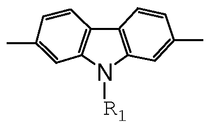
- Carbazole Wherein is a side chain having one or more of an amine group, a quaternary ammonium salt group, a nitrile group, a carboxyl group, a sulfonic acid group, and a phosphoric acid group; wherein B is a component not containing a polar or ionic group, and has the following One or several structures:
- R4 is H, d_C 2 .
- Carbazole an alkyl group wherein R 3 is H, C "C 2 .
- C is an aromatic heterocyclic unit containing sulfur, silicon, nitrogen, and selenium, and has the following one
- X is thioquine and its derivatives thiophene and its derivatives selenophene and its derivatives
- X is sulfur (S) or selenium (Se), R 9 and Rio- are H,
- Silole derivatives Wherein X is sulfur (S) or selenium (Se), Rn, Ri2- is H, or ⁇ . Alkyl, or p-phenyl.
- the photoactive layer is composed of a conjugated polymer (such as polythiophene and its derivatives, poly(p-phenylene) and its derivatives, polyfluorene and its derivatives , polycarbazole and its derivatives, polythiazole and its derivatives) as electron donor materials, carbon 60 and its derivatives (for example, [6,6]-phenyl-C 61 -butyric acid methyl ester ( PC 61 BM)) or carbon 70 and its derivatives (for example, [6,6]-phenyl-C71-butyric acid methyl ester (PC 71 BM)) or inorganic semiconductor nanoparticles (for example, zinc oxide, titanium dioxide, lanthanum Cadmium, etc.) as an electron acceptor material, an electron donor material and an electron acceptor material are combined in an organic solvent, and are subjected to spin coating, brush coating, spray coating, dip coating, roll coating, screen printing, printing or ink je
- a conjugated polymer such as polythiophene and its derivative
- the photoactive layer is a conjugated polymer as an electron donor material, and carbon 60 and its derivatives or carbon 70 and its derivatives or inorganic semiconductor nanoparticles are used as The electron acceptor material is laminated.
- the photoactive layer is made of an organic small molecule semiconductor material (for example, an acene, an anthraquinone, a thiophene oligomer) as an electron donor material, and a carbon 60
- an organic small molecule semiconductor material for example, an acene, an anthraquinone, a thiophene oligomer
- the derivative thereof or carbon 70 and its derivatives or inorganic semiconductor nanoparticles are laminated as an electron acceptor material.
- the above method for preparing a polymer bulk heterojunction solar cell with inverted structure is characterized in that a polymer as a cathode interface layer is dissolved in a polar organic solvent to prepare a solution, and the solution concentration is 0.0001-0.10 g/cm 3 ;
- the solution is formed into a cathode interface layer on the photoactive layer by spin coating, brushing, spraying, dip coating, roll coating, screen printing, printing or ink jet printing, and has a thickness of 0.1 to 100 nm.
- the polar organic solvent is an alcohol or a mixed solvent of an alcohol and water.
- the above method for preparing a polymer bulk heterojunction solar cell of an inverted structure wherein the cathode is an indium tin oxide conductive film (ITO), a fluorine-doped tin dioxide (FTO), a metal film, or a metal oxide film.
- ITO indium tin oxide conductive film
- FTO fluorine-doped tin dioxide
- metal film or a metal oxide film.
- the invention can greatly improve the performance of the polymer body heterojunction solar cell of the inverted structure and prolong the life of the polymer body heterojunction solar cell; the invention adopts the solution processing technology, the preparation process is simple, and the manufacturing cost is low.
- the present invention has the following advantages: (1) The device structure and method according to the present invention can greatly improve the performance of the polymer bulk heterojunction solar cell device, especially the energy conversion efficiency and the short-circuit current.
- the device structure of the present invention can extend the life of a polymer bulk heterojunction solar cell.
- the device structure involved in the invention adopts a solution processing technique, and the preparation process is simple, and the manufacturing cost is low.
- the solar cell according to the present invention can simultaneously adopt a film having a transmittance of 10% or more for a solar spectrum (wavelength in the range of 250-2400 nm) as an anode and a cathode electrode at both ends, thereby realizing a transparent or translucent sun. battery.
- FIG. 1 is a schematic view showing the structure of a polymer bulk heterojunction solar cell of a conventional structure.
- FIG. 2 is a schematic structural view of a polymer body heterojunction solar cell of an inverted structure provided by the present invention, wherein
- Figure 3 compares the performance decay curves of the inverted structure device and the conventional structure device provided by the present invention.
- the same batch of ITO conductive glass substrate is 15 mm x 15 mm, the thickness of ITO is about 130 nm, and the sheet resistance is about 20 ohms/square.
- the surface of the ITO substrate was cleaned by ultrasonic treatment with acetone, micron-sized semiconductor-specific detergent, deionized water, and isopropyl alcohol for 10 minutes, and then placed in a constant temperature oven at 80 ° C for 4 hours to dry.
- the dried ITO substrate was treated with oxygen plasma for 4 minutes to remove the organic adhering film and organic contaminants adhering to the ITO surface, and then placed on a homogenizing machine (KW-4A type), and then on the dried ITO.
- a homogenizing machine KW-4A type
- a conjugated polymer of a polar unit containing a polar group or an ionic group, or a solution of its corresponding polyelectrolyte which is subjected to high-speed spin coating (600-6000 rpm) to obtain a cathode interface layer.
- the thickness is between 0.1 and 100 nm.
- the cathode interface layer material is a conjugated polymer containing polar groups of polar groups or ionic groups, or a corresponding polyelectrolyte thereof, which has been proven to be an excellent electron transport material,
- the high work function metal provides an ohmic contact, and the preparation method thereof is described in the Chinese invention patent "Organic / Polymer Light Emitting Diode” (Patent No.: ZL200310117518.5), which is placed in a clean vial and transferred to a nitrogen protective film.
- a solution of 0.0001-0.10 g/cm 3 is dissolved in methanol with a small amount of acetic acid, placed on a stirring table and stirred uniformly, and filtered through a 0.45 ⁇ m filter to obtain a clear solution.
- the glass substrate iy cathode (2) / cathode interface layer (3) prepared by the above method was transferred to a special glove box (manufactured by American VAC Company) which is anhydrous and oxygen-free and filled with high-purity nitrogen.
- the glove box is inert.
- the polymer donor material and electron acceptor material carbon 60 derivative-[6,6]-phenyl-C 61 -butyric acid methyl ester (PC 61 BM), or carbon 70 derivative-[6 , 6]-phenyl-C71-methyl butyrate (PC 71 BM) was placed in a clean sample bottle, dissolved in a common organic solvent (such as chlorobenzene, toluene, etc.) to prepare a solution, placed on a heated mixing table. Stir well, fully dissolve to obtain a clear solution. Then mix the polymer donor material and electron acceptor material in a certain proportion, place it on a heating stirrer and stir evenly.
- a common organic solvent such as chlorobenzene, toluene, etc.
- the solution is prepared by mixing a donor material and an electron acceptor material.
- the glass substrate (1) / cathode (2) / cathode interface layer (3) is first adsorbed to the homogenate by a vacuum generated by a mechanical pump.
- On-board, after instillation of polymer donor material and electron acceptor material, after high-speed spin coating (600-6000 rpm) In general, it is required to produce a photoactive layer having a thickness of 20-500 nm, preferably a film thickness of 70-200 nm.
- the thickness is adjusted by adjusting the rotational speed of the homogenizer and controlling the polymer donor material and electron acceptor.
- the concentration of the material mixture solution was controlled.
- the thickness of the obtained film was recorded by a surface profiler (Teriek Alpha-Tencor 500 type).
- the device was transferred into a vacuum plating chamber, and the mechanical pump and the molecular pump were turned on. After a high vacuum of 3 x 10 -4 Pa was reached in the plating chamber, an aluminum film (100 nm) was vapor-deposited as an extraction electrode. If necessary, a thin film of a metal oxide (such as molybdenum oxide) is vapor-deposited before vapor deposition of the metal electrode to form a composite cathode. Depending on the situation, other metals with good air stability, such as gold, silver, etc., may be used as the electrodes.
- a metal oxide such as molybdenum oxide
- the growth settling rate and the total deposition thickness of the film are controlled by the applied heat power, and are monitored in real time by a quartz crystal film thickness monitor (STM-100 type, manufactured by Sycon Corporation).
- STM-100 type manufactured by Sycon Corporation.
- the UV-Vis absorption spectrum of the photoactive layer or polymer electron donor material was measured by a HP8453A diode array UV-Vis spectrophotometer with a wavelength range of 190 nm to 1100 nm.
- Solar cells are energy conversion devices. To convert solar energy into electrical energy, the determination of the performance parameters of any solar cell device is ultimately based on sunlight.
- the illuminance of the AM1.5G measurement standard commonly used in laboratories is 1000 watts per square meter.
- solar simulation light for polymer solar cell performance testing, first use a standard battery to determine whether the source is irradiance with AM1.5G. Standard silicon solar cells are calibrated: The short-circuit current is 125 mA under the AM1.5G standard spectrum, ie 1000 watts/m2 of irradiance. Once the irradiance is determined, the device can be tested. Solar cell performance test using solar simulation light can easily obtain the energy conversion efficiency of solar simulation light.
- the calculation method can be directly defined by:
- PMAX is the maximum output power (unit: milliwatts)
- ⁇ ⁇ is the irradiance (unit: milliwatts per square centimeter)
- S is the effective area of the device (unit: square centimeter).
- Lock-in amplifier 70100 Oriel weak signal detection
- Example 1 In order to show the effect of the inverted device structure used in the present invention on enhancing the performance of the polymer bulk heterojunction solar cell, an inverted structure device without a cathode interface layer was used as a comparative example using a conventional structural device.
- Example 1 In order to show the effect of the inverted device structure used in the present invention on enhancing the performance of the polymer bulk heterojunction solar cell, an inverted structure device without a cathode interface layer was used as a comparative example using a conventional structural device.
- the structure of the inverted structure polymer bulk heterojunction solar cell device shown in Fig. 2 is selected, and poly[9,9-dioctyl sulfonium-9,9-bis(N,N-dimethylaminopropyl) fluorene] is selected.
- PFNM ⁇ is the cathode interface layer
- benzodithiophene derivative (PTB7) is used as the polymer electron donor material
- carbon 70 derivative-[6,6]-phenyl-C71-butyric acid methyl ester (PC 71 BM) is An electron acceptor material, an inverted structure polymer bulk heterojunction solar cell was prepared.
- the polymer bulk heterojunction solar cell comprises a glass substrate 1, a cathode 2, a cathode interface layer 3, and a photoactive layer 4, And the anode 5 is sequentially laminated (as shown in FIG. 2), and a cathode interface layer 3 is provided between the cathode 2 and the photoactive layer 4, and the cathode interface layer 3 adopts a polarity containing a polar group or an ionic group.
- the conjugated polymer of the unit, or its corresponding poly dielectric
- the method is prepared by dissolving a conjugated polymer of a polar group or a ionic group-containing polar unit of the cathode interface layer 3 or a corresponding polyelectrolyte thereof in a polar organic solvent to prepare a solution having a solution concentration of 0.0001-0.10 g/cm 3 ; and the cathode interface layer 3 is formed on the cathode 2 by spin coating, brushing, spraying, dip coating, roll coating, screen printing, printing or ink jet printing.
- Table 2 compares the conventional device (the formal structure) with the device structure of ITO/PEDOT:PSS/PTB7:PC 71 BM/PFN/Al, and the device structure is ITO/PFN/PTB7:PC 71 BM/Mo0 3 /Al Inverted solar cells, and the performance of inverted solar cells that do not contain a cathode interface layer.
- Figure 3 compares the performance degradation curves of the inverted structure device and the conventional device provided by the present invention. It can be seen that the performance of the inverted structure device provided by the present invention decreases slowly over time, indicating that the inverted structure device provided by the present invention has better device stability and lifetime.
- ITO/PFN/PTB7 PC 7 iBM/Mo0 3 /Al
- ITO/ZnO/PFN/PTB7 PC 7 iBM/Mo0 3 /Al
- Example 1 was repeated, and a composite translucent film of MoO 3 (10 nm) / Ag (20 nm) was used as the anode.
- the measured solar cells were incident on the ITO surface (cathode) and the silver film surface (anode), respectively, and the measured properties are summarized in Table 4.
- the two-way transparent solar cell has the ability to operate in the case of bidirectional incidence compared to conventional devices that can only accept sunlight (including simulated sunlight) from the ITO transparent electrode. It is indicated that the inverted structure proposed by the present invention expands the role of polymer solar cells in other fields, such as solar power curtains and building exterior walls, and transparent self-generating devices.
Landscapes
- Chemical & Material Sciences (AREA)
- Physics & Mathematics (AREA)
- Engineering & Computer Science (AREA)
- Medicinal Chemistry (AREA)
- Polymers & Plastics (AREA)
- Organic Chemistry (AREA)
- Health & Medical Sciences (AREA)
- Chemical Kinetics & Catalysis (AREA)
- Nanotechnology (AREA)
- Electromagnetism (AREA)
- Mathematical Physics (AREA)
- Theoretical Computer Science (AREA)
- Crystallography & Structural Chemistry (AREA)
- Photovoltaic Devices (AREA)
Abstract
提供了一种倒置结构的聚合物本体异质结太阳电池及其制备方法。聚合物本体异质结太阳电池包括依次层叠的玻璃衬底(1)、阴极(2)、阴极界面层(3)、光活性层(4)和阳极(5)。制备方法为将作为阴极界面层的含有极性基团或离子性基团的极性单元的共轭聚合物,或者其对应的聚电介质溶于极性有机溶剂中制备成溶液,溶液浓度为0.0001-0.10克/立方厘米;并将该溶液采用旋涂、刷涂、喷涂、浸涂、辊涂、丝网印刷、印刷或喷墨打印方式在阴极上形成阴极界面层。这样可大幅提高聚合物本体异质结太阳电池的性能并延长其寿命;采用溶液加工技术,制备工艺简单,制作成本低。
Description
一种倒置结构的聚合物本体异质结太阳电池及其制备方法 技术领域
本发明涉及聚合物本体异质结太阳电池的技术领域,具体涉及倒置结构的聚合物 本体异质结太阳电池及其制备方法。
背景技术
基于光伏效应将太阳能转化为电能的太阳电池一直是国内外研究的热点。随着全 球能源需求的逐年增加, 石油、煤炭等一次性能源的日渐枯竭, 以及出于保护地球环 境等需要, 人们把越来越多的目光投向了太阳能、 氢能等可再生能源。
目前, 市场上成熟的太阳电池主要为基于单晶硅、 多晶硅、 非晶硅、 砷化镓、 磷 化铟以及多晶膜化合物半导体等无机太阳能电池,其中, 多晶硅和非晶硅太阳能电池 在民用太阳能电池市场上占主导地位。经过五十余年的发展,无机单晶硅太阳电池的 光电转换效率已经由发明之初的 6%, 提高到目前的最高效率可达 30%以上。 在基于 硅的太阳电池当中, 第一代的单晶硅太阳电池的能量转换效率可达 20 %, 接近 Shockley等人所预言 33 %的上限 [W. S. hocley and H. J. Queisser. Detail balance limit of efficiency of PN junction solar cells. J. Appl. Phys. 1961, 32: 510], 第二代 5-10%, 第三 代超过 50 %, 接近热力学上的上限值 93 % [Progress in photovoltaic: research and application, vol. 9-123 (2001)]。 尽管如此, 但是由于无机半导体太阳电池对材料纯度 的要求非常高,且价格昂贵,因此其应用受到很大限制。
利用有机半导体制备光伏器件首先在 1986年取得突破。当时美国柯达公司研究人 员 C.W. Tang首次在同一器件中引入给体和受体材料, 效率达到 1%[ C. W. Tang, Appl. Phys. Lett. 48, 183 (1986).]。这一异质结的概念成为目前所有三种有机光伏器件,染料 敏化器件, 平面型有机太阳电池, 以及本体异质结结构的关键思想。异质结这一概念 的精髓在于: 使用两种电子亲合能和电离势不同的材料混合。在界面处, 电势差足以 使到激子离解, 只要这一能量差比激子的束缚能大: 电子被具有较高电子亲合能的材 料接收,而空穴被具有较低电离势的材料接收。在平面异质结 (双层)结构中,有机 D/A 界面分离激子的效率比单层器件中电极 /有机物界面的分离效率高得多。 在这种类型
的器件中, 激子应在位于扩散距离之内的范围形成, 否则激子发生衰退, 对形成光电 流毫无贡献。 由于激子在有机材料中的扩散距离远远比薄膜的吸收厚度小, 从而限制 了有效吸收太阳光的薄膜厚度。
1992年 Sariciftci等在对 MEH-PPV/C6Q复合体系的研究中发现二者在基态没有 相互作用,但是 C6Q对 MEH-PPV 的荧光却有很强的猝灭作用,并提出体系中存在光诱 导电子转移过程 [Sariciftci N S, Smilowitz L, Heeger A J, et al . Photoinduced electron transfer from a conducting polymer to Buckminsterflillerene, Science ,1992 ,258 :1474.]。 共轭聚合 C6Q体系的光诱导电子转移理论提出以后,引起了科学工作者的极大兴趣,他 们采用多种实验方法,对不同的复合体系进行深入研究,证明了光诱导电子转移的存 在。 这一过程在几个皮秒内完成, 比激子的辐射衰减和非辐射衰减要快 3-4个数量级 [Sariciftci N S, Smilowitz L, Heeger A J, et al . Photoinduced electron transfer from a conducting polymer to Buckminsterflillerene, Science, 1992,258 :1474; Sariciftci N.S.; Braun D.; Zhang C., et al. Semiconducting polymer-buckminsterfullerene heterojunctions: Diodes, photodiodes, and photovoltaic cells [J]. Applied Physics Letters, 1993, 62 (6): 585-587; Sariciftci N.S.; Smilowitz L.; Heeger A.J., et al. Semiconducting polymers (as donors) and buckminsterflillerene (as acceptor): photoinduced electron transfer and heterojunction devices [J]. Synthetic Metals, 1993, 59 (3): 333-352.], 这样可以有效地阻 止光激发产生的电子和空穴再发生复合, 从而使得电荷分离的效率接近 100 %。光诱 导电荷快速能量转移现象的发现是聚合物太阳电池理论方面的重大突破,为聚合物太 阳电池效率的提高提供了理论支持。 而与之形成对比的是, 对于 MIM结构, 激子离 解的份额仅在 10%左右, 表明激子易于复合, 或者被陷阱态俘获, 造成效率很低, 无实用价值。
1995 年 G. Yu 等人通过将电子给体材料与受体材料共混, 制得共轭聚合物 MEH-PPV和碳 60互穿网络结构的太阳电池,其能量转换效率达到 2.9%[ Yu G; Gao J.; Hummelen J.C., et al. Polymer photovoltaic cells: Enhanced efficiencies via a network of internal donor-acceptor heterojunctions. Science, 1995, 270: 1789-1791]。 在这种体系中, 电子给体材料 (D)与受体材料 (A)形成双连续的互穿网络状结构 (bi-continuous network),这种结构大大增大了 D/A界面面积,使异质结更加分散, 在激子的扩散距离 非常有限的情况下, 由于在所产生的激子附近具有与受体材料形成的界面, 从而可以 确保快速的激子离解的发生,产生电荷分离。产生的电荷在各自的相中输运并在相应
的电极上被收集,光生载流子在到达相应的电极前被重新复合的几率大为降低, 结果 其光电转换效率,或者说光敏是纯 MEH-PPV器件的 100多倍。这种将 D/A异质结结 构分散到整个活性层的创新, 实际上将整个活性层变为一个大的所谓"本体异质结" (Bulk Heterojunction, BHJ), 换言之, 在活性层中的任何位置均可产生电荷。 只要各 相材料形成从 D/A界面到各自电极的连续通道, 那么, 由光子到电子的转换效率可 以得到很大的提高。 这就是聚合物本体异质结太阳电池的发明和出现 [美国专利 5331183(1994)和美国专利 5454880(1995)]。
体异质结概念产生克服了单层、 双层 /多层器件的结构缺陷。 由于电子给体与电 子受体各自形成网络状连续相,光诱导所产生的电子与空穴分别在各自的相中输运并 在相应的电极上被收集, 光生载流子在到达相应的电极前被重新复合的几率大大降 低, 从而提高了光电流。 这样, 体异质结结构就能大幅度的提高光电能量转换效率。 如今, 体异质结概念已广泛用于基于聚合物的太阳电池, 能量转换效率已能达到 5 % 以上。可以看出, 聚合物本体异质结太阳电池的出现, 指引着有机太阳电池的发展方 向。
从此, 结合共轭聚合物所兼备的优良半导体特性, 机械加工特性, 可在室温下以 配制溶液, 然后通过旋转涂膜、 喷涂等成膜, 或者用喷墨打印的方式, 可以制备成本 低廉的大面积太阳电池。 除此之外, 相对传统硅基太阳电池, 有机太阳电池还有无需 高温高真空处理工序, 无需依赖高纯度的材料等显著优点, 代表着诱人的发展前景。 然而, 目前有机太阳电池的最高能量转换效率为 8%左右, 距离商业化还有一段 较大的距离。 因此, 有机太阳电池的研究也面临很大的挑战, 只有获得高效率更高, 性能稳定的器件,才能其商业化的生产,应用于目前无机太阳电池所应用的所有领域。
为了提高其能量转换效率, 众多的化学家、物理学家和材料学家从材料合成、器 件结构、 器件制备等角度入手, 对聚合物太阳电池进行了深入的研究。 目前, 聚合物 本体异质结太阳电池还存在一些问题, 使其性能受到制约, 这些挑战主要包括: 1) 作为 p型半导体和光活性层的聚合物材料多为无定形结构, 结晶度较低, 分子间作用 力较弱, 光生载流子主要在分子内的共轭键上运动, 而在分子间的迁移则比较困难, 从而导致材料的载流子迁移率较低 (10—4 cm2 V— 1 s -1),光生载流子在被收集形成外电流 之前容易发生复合而损耗。 因此, 造成器件的短路电流和填充因子偏低; 2)大部分共 轭聚合物的吸收波段都集中在可见光范围, 活性层的光谱响应范围比较窄,对红外区
域的太阳辐射利用率较低, 导致电池的响应光谱与太阳能地面辐射不匹配。 因此, 对 太阳光的利用率比较低, 影响能量转换效率; 3) 聚合物本体异质结太阳电池还存在 一个技术上的瓶颈, 高的开路电压和对太阳光宽范围的吸收很难以同时兼得。这是因 为, 器件的开路电压 V。c, 内建电势 Vbl由给体材料的最高占有轨道 (HOMO)能级和受 体材料的最低未占有轨道 (LUMO)能级的差值确定。 要提高器件的开路电压, 往往要 降低给体材料的最高占有轨道 (HOMO)能级 (因为受体材料的 LUMO能级相对能够改 动的空间不大),这就意味着给体材料的带隙变宽,与太阳光谱的匹配程度下降。4)在 器件稳定性及寿命方面, 与实用化的要求相比, 还有很大的差距。
一般来说,常规聚合物本体异质结太阳电池的结构由玻璃衬底、阳极及其缓冲层、 光活性层和阴极依次层叠构成 (如图 1所示)。 简单而言, 就是阳极在玻璃衬底上, 阴 极在外表面上, 由最后的镀膜制备工序制备。
发明内容
本发明的目的在于克服现有技术存在的上述不足,提出倒置结构的聚合物本体异 质结太阳电池及其制备方法, 具体技术方案如下。
所述聚合物本体异质结太阳电池包括依次层叠的玻璃衬底、 阴极、 阴极界面层、 光活性层和阳极依次层叠,在阴极与光活性层之间设阴极界面层,所述阴极界面层采 用含有极性基团或离子性基团的极性单元的共轭聚合物, 或者其对应的聚电介质构 成。
上述倒置结构的聚合物本体异质结太阳电池中,所述光活性层由共轭聚合物和富 勒烯衍生物的混合物组成的。
本发明中所使用的阴极界面层材料, 其代表结构在中国发明专利 "有机 /高分子发 光二极管",(中国专利号: ZL200310117518.5)已有 有极

性基团或离子性基团的极性单元的共轭聚合物: , 其中 (0.5≤x≤l; 0≤y+ z≤0.5; x+y+z=l); 聚合度 (n)为 1-300之间的任意整数;
A 为含有极性基团或离子性基团的极性共轭单元, 具有如下其中一种或多种结 构的组合:
芴:
 其中 R2为带有胺基、 季铵盐基、 腈基、 羧基、 磺酸基、 磷酸基其中一 的侧链;
对苯:
 其中 R2为带有胺基、 季铵盐基、 腈基、 羧基、 磺酸基、 磷酸基其中一个
螺旋-对苯:
 其中 , R2为带有胺基、 季铵盐基、 腈基、 羧 磺酸基、 磷酸基其中一个或多个的侧链;
咔唑:
 其中 为带有胺基、 季铵盐基、 腈基、 羧基、 磺酸基、 磷酸基其中一个或多个的侧链; 其中 B 为不含有极性或离子性基团的组分, 具有如下的一种或几种结构:
, R4为 H, d_C2。的烷基;
为 H, C「C2。的烷基, 烷氧基;
螺
 旋-对苯: 其中 R3, R4为 H, d—C^的;)

咔唑: 其中 R3为 H, C「C2。的烷基;
C为含有硫, 硅, 氮, 硒的芳杂环单元, 具有如下的一
苯 并 噻 ( 硒 ) 二 唑 及 其 衍 生 物 :


其中, X为硫 喹啉及其衍生物 噻吩及其衍生物 硒吩及其衍生物
喹喔啉衍生物:

其中, X为硫 (S)或硒 (Se), R9,Rio- 为 H,
噻 咯 (Silole) 衍 生 物 :

 其中, X为硫 (S)或硒 (Se), Rn,Ri2- 为 H,或 〜 。的烷基, 或对苯基。
上述的倒置结构的聚合物本体异质结太阳电池,所述光活性层由共轭聚合物(如 聚噻吩及其衍生物,聚对苯撑乙及其烯衍生物,聚芴及其衍生物,聚咔唑及其衍生物, 聚噻咯及其衍生物) 作为电子给体材料,, 碳 60及其衍生物 (例如, [6,6]-苯基 -C 61 - 丁酸甲酯 (PC61BM))或者碳 70及其衍生物 (例如, [6,6]-苯基 -C71 -丁酸甲酯 (PC71BM)) 或者无机半导体纳米颗粒 (例如, 氧化锌, 二氧化钛, 碲化镉等)作为电子受体材料, 电子给体材料和电子受体材料在有机溶剂中组成混合溶液, 经旋涂、 刷涂、 喷涂、 浸 涂、 辊涂、 丝网印刷、 印刷或喷墨打印方式形成光活性层。
上述的倒置结构的聚合物本体异质结太阳电池,所述光活性层以共轭聚合物作为 电子给体材料,和碳 60及其衍生物或者碳 70及其衍生物或者无机半导体纳米颗粒作 为电子受体材料叠层构成。
上述的倒置结构的聚合物本体异质结太阳电池,所述光活性层以有机小分子半导 体材料(例如, 并苯类, 酞氰类, 噻吩寡聚物)作为电子给体材料, 和碳 60及其衍生 物或者碳 70及其衍生物或者无机半导体纳米颗粒作为电子受体材料叠层构成。
上述的倒置结构的聚合物本体异质结太阳电池的制备方法,其特点在于将作为阴 极界面层的聚合物溶于极性有机溶剂中制备成溶液, 溶液浓度为 0.0001-0.10克 /立方 厘米; 并将所述溶液采用旋涂、 刷涂、 喷涂、 浸涂、 辊涂、 丝网印刷、 印刷或喷墨打 印方式在光活性层上形成阴极界面层, 其厚度为 0.1〜100纳米。 所述极性有机溶剂 为醇或醇与水的混合溶剂。
上述的倒置结构的聚合物本体异质结太阳电池的制备方法,所述阴极为氧化铟锡 导电膜 (ITO), 掺氟二氧化锡 (FTO), 金属膜, 或者金属氧化物薄膜中的其中一种或其 组合。
本发明可大幅提高倒置结构的聚合物本体异质结太阳电池的性能,延长聚合物本 体异质结太阳电池的寿命; 本发明采用溶液加工技术, 制备工艺简单, 制作成本低。
与现有技术相比, 本发明具有如下优点:
( 1 ) 本发明涉及的器件结构、 方法可大幅提高聚合物本体异质结太阳电池器件 的性能, 尤其是能量转化效率和短路电流这两项重要指标。
(2) 本发明涉及的器件结构可延长聚合物本体异质结太阳电池的寿命。
(3 ) 本发明涉及的器件结构采用溶液加工技术, 制备工艺简单, 制作成本低。
(4) 本发明涉及的太阳电池, 可同时采用对太阳光谱 (波长处于 250-2400 纳米 的范围)具有 10%以上的透射率的薄膜作为两端的阳极和阴极电极, 实现透明或者半 透明的太阳电池。 附图说明
图 1为常规结构的聚合物本体异质结太阳电池的结构示意图。
图 2为本发明提供的倒置结构的聚合物本体异质结太阳电池的结构示意图,其中,
1-玻璃衬底; 2-阴极; 3-阴极界面层; 4-光活性层; 5-阳极。
图 3比较了本发明提供的倒置结构器件与常规结构器件的性能衰减曲线。
具体实施方式
以下实例将对本发明所提出的具体工艺过程进行说明, 但本发明不限于所列之 例。
同批号 ITO导电玻璃衬底若干, 规格为 15毫米 xl5毫米, ITO的厚度约为 130 纳米, 其方块电阻约为 20欧姆 /方块。 依次用丙酮、 微米级半导体专用洗涤剂、 去离 子水、异丙醇超声处理 10分钟清洁 ITO衬底表面, 随后放入恒温烘箱中 80°C下静置 4小时烘干。烘干后的 ITO衬底用氧等离子体处理 4分钟, 除去 ITO表面附着的有机 附着薄膜和有机污染物, 后置于匀胶机 (KW-4A型)上, 再在烘干的 ITO上面, 滴注 含有极性基团或离子性基团的极性单元的共轭聚合物, 或者其对应的聚电介质的溶 液, 经高速旋涂 (600-6000转 /分钟), 获得的阴极界面层的厚度在 0.1-100纳米。 所述 阴极界面层材料采用含有极性基团或离子性基团的极性单元的共轭聚合物,或者其对 应的聚电介质, 这些材料已经被证实是一种优良的电子传输材料, 可对高功函数金属 提供欧姆接触, 提供其制备方法在中国发明专利"有机 /高分子发光二极管"(专利号: ZL200310117518.5)中已描述, 将其置于洁净小瓶中, 转入氮气保护成膜专用手套箱 中, 在加有少量乙酸的甲醇中溶解配成 0.0001-0.10克 /立方厘米的溶液, 置于搅拌台 上搅拌均匀, 用 0.45微米滤膜过滤得澄清溶液。
随后将由上述方法制得的玻璃衬底 (iy阴极 (2)/阴极界面层 (3)转入无水无氧、充满 高纯氮气的专用手套箱 (美国 VAC 公司制造)。 在此手套箱惰性气氛下, 将聚合物给 体材料和电子受体材料, 碳 60衍生物 -[6,6]-苯基 -C 61 -丁酸甲酯 (PC61BM), 或者碳 70衍生物 -[6,6]-苯基 -C71 -丁酸甲酯 (PC71BM)分别置于洁净试样瓶中, 用常用有机溶 剂 (如氯苯, 甲苯等)溶解配制成溶液, 放置在加热搅拌台上搅拌均匀, 充分溶解后得 到澄清溶液。然后按一定的比例将聚合物给体材料和电子受体材料混合,放置在加热 搅拌台上搅拌均匀。光活性层的制备通过在衬底上涂覆聚合物给体材料和电子受体材 料混合的溶液制得。为此,首先将将玻璃衬底 (1)/阴极 (2)/阴极界面层 (3)通过机械泵产 生的负压吸附在匀胶机上, 滴注聚合物给体材料和电子受体材料混合溶后, 经高速旋 涂 (600-6000转 /分钟)制得, 一般而言, 要求制得的光活性层厚度在 20-500纳米, 优 选薄膜厚度为 70-200纳米。 厚度通过调节匀胶机的转速以及控制聚合物给体材料和 电子受体材料混合溶液的浓度来控制。 制备过程中, 所得薄膜的厚度由表面轮廓仪 (Teriek公司 Alpha-Tencor500型)实测记录。
随后, 将器件转入真空镀腔中, 开启机械泵和分子泵, 当镀腔内达到 3x10— 4Pa 的高真空以后, 开始蒸镀铝膜 (100纳米)作为引出电极。 在有必要的情况下, 还在蒸 镀金属电极前蒸镀金属氧化物 (如氧化钼等)薄膜,组成复合型的阴极。根据具体情况, 或选用其它空气稳定性好的金属, 如金, 银等作为电极。 为了使到上述真空热蒸发金 属薄膜过程, 薄膜的生长沉降速率和总的沉积厚度由施加的热功率控制, 并通过石英 晶振膜厚监测仪 (STM-100型, Sycon公司制造)实时监控。 光活性层或者聚合物电子 给体材料的紫外 -可见光吸收光谱由 HP8453A型二极管阵列式紫外-可见分光光度计 测得, 测试的波长范围 190 纳米〜 1100 纳米。
太阳电池是能量转换器件, 要将太阳能转换为电能, 所以任何太阳电池器件性能 参数的测定, 最终都要以太阳光为测试标准。 实验室中常用的 AM1.5G测量标准的辐 射照度是 1000瓦 /平方米。 当用太阳模拟光进行聚合物太阳电池性能测试时, 首先要 用标准电池确定光源是否复合 AM1.5G的辐照度。 标准硅太阳电池经过校准: 在 AM1.5G标准光谱下,即 1000瓦 /平方米的辐射照度的光照射下,得到的短路电流为 125 毫安。确定辐照强度后,即可对器件进行测试。用太阳模拟光进行太阳电池性能测试, 可以方便地得出太阳模拟光的能量转换效率, 其计算方法可直接由定义得到:

其中 PMAX为最大输出功率 (单位: 毫瓦), ΡΙΗ为辐射照度 (单位: 毫瓦 /平方厘米), S 为 器件的有效面积 (单位: 平方厘米)。 测量聚合物本体异质结太阳电池性能的设备装置 如表 1所示。
表 1
设备名称 规格 /型号 供应商 功能
模拟太阳光源 91192 Oriel 太阳模拟光源 斩波器 75152 Oriel 测定器件的光敏, 外 单色仪 74000 Oriel 量子效率
锁相放大器 70100 Oriel 微弱信号检测
AM0滤波片 Oriel
提供标准模拟太阳光 AMI滤波片
 Oriel
Oriel
天津 18所或
校正模拟太阳光源的 标准硅太阳电池 滨松公司
辐照强度
(型号: S1133)
2400电压一电流源 2400 Keithley 太阳电池的伏安特性
236电压一电流源 236 Keithley 测量
为显示本发明所采用的倒置器件结构在增强聚合物本体异质结太阳电池性能上 的效果, 另外采用常规结构器件, 不含阴极界面层的倒置结构器件作为对照例。 实施例 1
选用图 2所示的倒置结构聚合物本体异质结太阳电池器件结构,选用聚 [9, 9一二辛 基芴一 9, 9一双 (N, N—二甲基胺丙基)芴] (PFNM乍为阴极界面层, 苯并二噻吩衍生 物 (PTB7)作为聚合物电子给体材料, 碳 70衍生物 -[6,6]-苯基 -C71 -丁酸甲酯 (PC71BM) 为电子受体材料, 制备了倒置结构聚合物本体异质结太阳电池。
所述聚合物本体异质结太阳电池由玻璃衬底 1、阴极 2、阴极界面层 3、光活性层 4,
和阳极 5依次层叠构成 (如图 2所示), 在阴极 2与光活性层 4之间设阴极界面层 3, 所述 阴极界面层 3采用含有极性基团或离子性基团的极性单元的共轭聚合物, 或者其对应 的聚电介质构成。 所述方法将作为阴极界面层 3的含有极性基团或离子性基团的极性 单元的共轭聚合物, 或者其对应的聚电介质溶于极性有机溶剂中制备成溶液, 溶液浓 度为 0.0001-0.10克 /立方厘米; 并将该溶液采用旋涂、 刷涂、 喷涂、 浸涂、 辊涂、 丝网 印刷、 印刷或喷墨打印方式在阴极 2上形成阴极界面层 3。
表 2比较了器件结构为 ITO/PEDOT:PSS/PTB7:PC71BM/PFN/Al的常规器件 (;正装结 构), 与器件结构为 ITO/PFN/PTB7:PC71BM/Mo03/Al的倒置结构太阳电池, 以及不包 含阴极界面层的倒置结构太阳电池的性能。
由表 2可以看出, 以 PFN作为阴极界面层的倒置结构的聚合物本体异质结太阳 电池, 与常规器件相比, 能量转化效率和短路电流密度这两项参数均有 7%以上的提 高。 表明本发明提出的倒置结构具有改善器件性能的重要作用。
图 3比较了本发明提供的倒置结构器件与常规器件的性能衰减曲线。可以看出, 本发明提供的倒置结构器件的性能随时间流逝下降较慢,表明出本发明提供的倒置结 构器件具有更好的器件稳定性和寿命。
表 2 短路电流密度 开路电压 填充因子 能量转换 器件类型
(毫安 /平方厘米) (伏特) (%) 效率 (%) 倒置结构:
17.47 0.730 69.9 8.91
ITO/PFN/PTB7:PC7iBM/Mo03/Al
对照例
不包含阴极界面层的倒置结构:
16.36 0.67 54.8 5.99 ITO/ PTB7:PC71BM/Mo03/Al
常规结构 (正装) : 15.70 0.727 72.4 8.26
实施例 2
重复实施例 1, 选用氧化锌和聚 [9, 9一二辛基芴一 9, 9-¾(N, N—二甲基胺丙 基)芴] (PFNM乍为阴极界面层作为复合式的阴极界面层, 其它条件不变。 实验结果总
结于表 3。
由表 3可以看出, 以氧化锌和 PFN作为复合式的阴极界面层的倒置结构的聚合 物本体异质结太阳电池, 与不包含阴极界面层的倒置结构相比, 能量转化效率有所提 高。 表明本发明提出的倒置结构具有改善器件性能的重要作用。 表 3 短路电流密度 开路电压 填充因子 能量转换 器件类型
(毫安 /平方厘米) (伏特) (%) 效率 (%) 倒置结构:
16.02 0.74 69.8 8.27
ITO/ZnO/PFN/PTB7:PC7iBM/Mo03/Al
对照例
不包含阴极界面层的倒置结构:
16.36 0.67 54.8 5.99 ITO/ PTB7:PC71BM/Mo03/Al 实施例 3
重复实施例 1, 选用 MoO3(10 纳米 )/Ag(20 纳米)的复合式半透明薄膜作为阳极。 制得的太阳电池在入射光从 ITO表面 (阴极), 银膜表面 (阳极)分别入射的情况下, 测 得的性能汇总于表 4。
表 4 短路电流密度 开路电压 填充因子 能量转换 入射光射入方向
(毫安 /平方厘米) (伏特) (%) 效率 (%) 从阴极入射 (从 ITO表面) 14.67 0.68 61.4 6.13 从阳极入射 (从银膜表面) 13.25 0.65 57.6 4.96 由表 4可以看出, 制得的双向透明太阳电池, 与常规器件只能接受太阳光 (含模 拟太阳光)从 ITO透明电极入射相比, 具有可在双向入射的情况下工作的能力。 表明 本发明提出的倒置结构拓展聚合物太阳电池应用于其它领域,如太阳发电窗帘和建筑 外墙, 透明自发电器件等方面的重要作用。
Claims
1、 一种倒置结构的聚合物本体异质结太阳电池, 包括玻璃衬底 (1)、 阴极 (2)、 光 活性层 (4)和阳极 (5), 其特征在于还包括阴极界面层 (3), 所述玻璃衬底 (1)、 阴极 (2)、 阴极界面层 (3)、 光活性层 (4)和阳极 (5) 依次层叠; 所述阴极界面层 (3)的材料采用含 有极性基团或离子性基团的极性单元共轭聚合物或者它们对应的聚电介质。
2、 根据权利要求 1 所述的聚合物本体异质结太阳电池, 其特征在于所述含有极 性 聚合物具有如下结构:
 式中: x, y, z为分子摩尔分数, 且 0.5≤x≤l; 0<y+ z<0.5; x+y+z=l;聚合度 n为 1〜 300;
A 为含有极性基团或离子性基团的极性共轭单元, 具有如下其中一种或多种结 构的组合:


螺旋 -对苯 其中 , R2为带有胺基、 季铵盐基、 腈 基、 羧基、 磺酸基、 磷酸基中一个或多个的侧链;
咔唑:
 , 其中 为带有胺基、 季铵盐基、 腈基、 羧基、 磺酸 磷酸基中一个或多个的侧链;
Β 为非极性共轭单元, 具有如下的一种或几种结构:
, 其中 R3, R4为 H, d—C^的烷基;
 中 R3, R4为 H, d- 的烷基, 烷氧基; 螺旋- 其中 R3, R4为 H, d—C^的;) 咔唑:
 其中 R3为 H, 或 d—C^的烷基;
C 为含有硫, 硅, 氮, 硒的芳杂环单元, 具有如下的一
并 噻 ( 硒 ) 二 唑 及 其 衍 生 物


或

其中, X为硫或硒, RU,R12- 为 11或 〜 。的烷基或对苯基。
3. 根据权利要求 1 所述的倒置结构的聚合物本体异质结太阳电池, 其特征在于 所述光活性层 (4)由共轭聚合物作为电子给体材料, 碳 60及其衍生物或者碳 70及其
衍生物或者无机半导体纳米颗粒作为电子受体材料,电子给体材料和电子受体材料在 有机溶剂中组成混合溶液, 经旋涂、 刷涂、 喷涂、 浸涂、 辊涂、 丝网印刷、 印刷或喷 墨打印方式形成光活性层 (4)。
4. 根据权利要求 1 所述的聚合物本体异质结太阳电池, 其特征在于所述光活性 层 (4)以共轭聚合物作为电子给体材料, 和碳 60及其衍生物或者碳 70及其衍生物或 者无机半导体纳米颗粒作为电子受体材料叠层构成。
5. 根据权利要求 1所述的聚合物本体异质结太阳电池, 其特征在于所述光活性 层 (4)以有机小分子半导体材料作为电子给体材料, 和碳 60及其衍生物或者碳 70及 其衍生物或者无机半导体纳米颗粒作为电子受体材料叠层构成。
6. 根据权利要求 1所述的聚合物本体异质结太阳电池, 其特征在于所述光活性 层由共轭聚合物和富勒烯衍生物的混合物组成的
7. 制备权利要求 1〜6任一项所述的聚合物本体异质结太阳电池的方法, 其特征 在于将作为阴极界面层 (3)的含有极性基团或离子性基团的极性单元共轭聚合物, 或 者其对应的聚电介质溶于极性有机溶剂中制备成溶液, 溶液浓度为 0.0001-0.10克 /立 方厘米; 并将所述溶液采用旋涂、 刷涂、 喷涂、 浸涂、 辊涂、 丝网印刷、 印刷或喷墨 打印方式在阴极 (2)上形成阴极界面层 (3), 其厚度为 0.1〜100纳米。
8. 根据权利要求 7所述的制备方法, 其特征在于所述极性有机溶剂为醇或醇与 水的混合溶剂。
9. 根据权利要求 7所述的制备方法, 其特征在于所述阴极 (2)为氧化铟锡导电膜 (ITO), 掺氟二氧化锡 (FTO), 金属膜, 或者金属氧化物薄膜中的其中一种或多种组合。
Applications Claiming Priority (2)
| Application Number | Priority Date | Filing Date | Title |
|---|---|---|---|
| CN2011103090434A CN102386336B (zh) | 2011-10-12 | 2011-10-12 | 一种倒置结构的聚合物本体异质结太阳电池及其制备方法 |
| CN201110309043.4 | 2011-10-12 |
Publications (1)
| Publication Number | Publication Date |
|---|---|
| WO2013053216A1 true WO2013053216A1 (zh) | 2013-04-18 |
Family
ID=45825522
Family Applications (1)
| Application Number | Title | Priority Date | Filing Date |
|---|---|---|---|
| PCT/CN2012/072492 WO2013053216A1 (zh) | 2011-10-12 | 2012-03-17 | 一种倒置结构的聚合物本体异质结太阳电池及其制备方法 |
Country Status (2)
| Country | Link |
|---|---|
| CN (1) | CN102386336B (zh) |
| WO (1) | WO2013053216A1 (zh) |
Families Citing this family (7)
| Publication number | Priority date | Publication date | Assignee | Title |
|---|---|---|---|---|
| CN102637828B (zh) * | 2012-04-17 | 2015-01-21 | 中国科学院合肥物质科学研究院 | 一种有机薄膜太阳能电池的制备方法 |
| CN102820430A (zh) * | 2012-05-14 | 2012-12-12 | 华南理工大学 | 一种柔性有机/聚合物太阳电池及其制备方法 |
| CN103208588B (zh) * | 2013-03-19 | 2015-10-28 | 华南理工大学 | 一种倒置结构的有机/聚合物太阳能电池 |
| ITMI20131831A1 (it) * | 2013-11-05 | 2015-05-06 | Eni Spa | Celle solari polimeriche invertite e processo per la produzione delle stesse |
| US9868820B2 (en) * | 2014-08-29 | 2018-01-16 | Rohm And Haas Electronic Materials Llc | Polyarylene materials |
| CN105384917B (zh) * | 2015-11-10 | 2018-06-12 | 华南理工大学 | 侧链含有磺酸或者磺酸盐的共轭聚合物及其制备的平面倒置有机/无机杂化钙钛矿太阳电池 |
| CN110790904B (zh) * | 2018-08-03 | 2021-09-21 | 华南理工大学 | 基于非对称窄带隙杂环并喹啉吸电子单元共轭聚合物材料及其制备方法与应用 |
Citations (4)
| Publication number | Priority date | Publication date | Assignee | Title |
|---|---|---|---|---|
| CN101483221A (zh) * | 2009-01-20 | 2009-07-15 | 华南理工大学 | 聚合物本体异质结太阳电池及其制备方法 |
| KR20100130514A (ko) * | 2009-06-03 | 2010-12-13 | 삼성전자주식회사 | 유기 태양 전지 및 그 제조방법 |
| CN102027602A (zh) * | 2008-03-14 | 2011-04-20 | 朔荣有机光电科技公司 | 半透明太阳能电池 |
| US20110272029A1 (en) * | 2010-05-04 | 2011-11-10 | Samsung Electronics Co., Ltd. | Organic solar cell and method of making the same |
Family Cites Families (1)
| Publication number | Priority date | Publication date | Assignee | Title |
|---|---|---|---|---|
| CN101593812A (zh) * | 2009-07-02 | 2009-12-02 | 吉林大学 | 一种半透明倒置有机太阳能电池及其制备方法 |
-
2011
- 2011-10-12 CN CN2011103090434A patent/CN102386336B/zh active Active
-
2012
- 2012-03-17 WO PCT/CN2012/072492 patent/WO2013053216A1/zh active Application Filing
Patent Citations (4)
| Publication number | Priority date | Publication date | Assignee | Title |
|---|---|---|---|---|
| CN102027602A (zh) * | 2008-03-14 | 2011-04-20 | 朔荣有机光电科技公司 | 半透明太阳能电池 |
| CN101483221A (zh) * | 2009-01-20 | 2009-07-15 | 华南理工大学 | 聚合物本体异质结太阳电池及其制备方法 |
| KR20100130514A (ko) * | 2009-06-03 | 2010-12-13 | 삼성전자주식회사 | 유기 태양 전지 및 그 제조방법 |
| US20110272029A1 (en) * | 2010-05-04 | 2011-11-10 | Samsung Electronics Co., Ltd. | Organic solar cell and method of making the same |
Also Published As
| Publication number | Publication date |
|---|---|
| CN102386336B (zh) | 2013-07-24 |
| CN102386336A (zh) | 2012-03-21 |
Similar Documents
| Publication | Publication Date | Title |
|---|---|---|
| Yang et al. | Solution-processed fullerene-based organic Schottky junction devices for large-open-circuit-voltage organic solar cells | |
| Chen et al. | Efficient polymer solar cells with thin active layers based on alternating polyfluorene copolymer/fullerene bulk heterojunctions | |
| CN101483221B (zh) | 聚合物本体异质结太阳电池及其制备方法 | |
| Zhang et al. | A solution-processed barium hydroxide modified aluminum doped zinc oxide layer for highly efficient inverted organic solar cells | |
| WO2013053216A1 (zh) | 一种倒置结构的聚合物本体异质结太阳电池及其制备方法 | |
| Mabrouk et al. | Synergistic engineering of hole transport materials in perovskite solar cells | |
| Pan et al. | All-solution processed double-decked PEDOT: PSS/V2O5 nanowires as buffer layer of high performance polymer photovoltaic cells | |
| JP7281216B2 (ja) | 有機光起電装置のためのハイブリッド平面混合ヘテロ接合 | |
| Raïssi et al. | Enhancing the short-circuit current, efficiency of inverted organic solar cells using tetra sulfonic copper phthalocyanine (TS-CuPc) as electron transporting layer | |
| Ismail et al. | Improvement in light harvesting and performance of P3HT: PCBM solar cell by using 9, 10-diphenylanthracene | |
| Gil-Escrig et al. | Interface engineering in efficient vacuum deposited perovskite solar cells | |
| JP2016500919A (ja) | スクアラインドナー添加剤を用いた高分子光起電技術 | |
| Ismail et al. | Effect of composition on conjugation structure and energy gap of P3HT: PCBM organic solar cell | |
| Wang et al. | Efficient ternary organic photovoltaic cells with better trade-off photon harvesting and phase separation by doping DIB-SQ | |
| Yu et al. | Fabrication and optimization of polymer solar cells based on P3HT: PC 70 BM system | |
| Li et al. | A dopant‐free polymer as hole‐transporting material for highly efficient and stable perovskite solar cells | |
| Sharma et al. | Photovoltaic properties of bulk heterojunction devices based on CuI-PVA as electron donor and PCBM and modified PCBM as electron acceptor | |
| Gautam et al. | AD–π–A1–π–A2 push–pull small molecule donor for solution processed bulk heterojunction organic solar cells | |
| Lei et al. | Wavelength-dependent charge carrier dynamics: the case of Ag2S/organic thin films heterojunction solar cells | |
| JP2017525151A (ja) | 高いガラス転移温度の材料を用いた励起子阻止電荷キャリアフィルタを含む安定した有機感光性デバイス | |
| JP2014090093A (ja) | タンデム型有機薄膜太陽電池 | |
| Saranin et al. | Solar cell manufacturing method with the structure of the bulk heterojunction based on organic semiconductors with a direct architecture | |
| Ismail et al. | Investigation of PCBM concentration on the performance of small organic solar cell | |
| Xiao et al. | Efficiency enhancement in polymer solar cells with a polar small molecule both at interface and in the bulk heterojunction layer | |
| Saravanan et al. | ZnO nanoparticles with different concentrations inside organic solar cell active layer |
Legal Events
| Date | Code | Title | Description |
|---|---|---|---|
| 121 | Ep: the epo has been informed by wipo that ep was designated in this application |
Ref document number: 12840673 Country of ref document: EP Kind code of ref document: A1 |
|
| NENP | Non-entry into the national phase |
Ref country code: DE |
|
| 122 | Ep: pct application non-entry in european phase |
Ref document number: 12840673 Country of ref document: EP Kind code of ref document: A1 |