WO2013021940A1 - 照明装置、表示装置、及びテレビ受信装置 - Google Patents
照明装置、表示装置、及びテレビ受信装置 Download PDFInfo
- Publication number
- WO2013021940A1 WO2013021940A1 PCT/JP2012/069832 JP2012069832W WO2013021940A1 WO 2013021940 A1 WO2013021940 A1 WO 2013021940A1 JP 2012069832 W JP2012069832 W JP 2012069832W WO 2013021940 A1 WO2013021940 A1 WO 2013021940A1
- Authority
- WO
- WIPO (PCT)
- Prior art keywords
- led
- light source
- light
- chassis
- board
- Prior art date
- Legal status (The legal status is an assumption and is not a legal conclusion. Google has not performed a legal analysis and makes no representation as to the accuracy of the status listed.)
- Ceased
Links
Images





Classifications
-
- G—PHYSICS
- G02—OPTICS
- G02F—OPTICAL DEVICES OR ARRANGEMENTS FOR THE CONTROL OF LIGHT BY MODIFICATION OF THE OPTICAL PROPERTIES OF THE MEDIA OF THE ELEMENTS INVOLVED THEREIN; NON-LINEAR OPTICS; FREQUENCY-CHANGING OF LIGHT; OPTICAL LOGIC ELEMENTS; OPTICAL ANALOGUE/DIGITAL CONVERTERS
- G02F1/00—Devices or arrangements for the control of the intensity, colour, phase, polarisation or direction of light arriving from an independent light source, e.g. switching, gating or modulating; Non-linear optics
- G02F1/01—Devices or arrangements for the control of the intensity, colour, phase, polarisation or direction of light arriving from an independent light source, e.g. switching, gating or modulating; Non-linear optics for the control of the intensity, phase, polarisation or colour
- G02F1/13—Devices or arrangements for the control of the intensity, colour, phase, polarisation or direction of light arriving from an independent light source, e.g. switching, gating or modulating; Non-linear optics for the control of the intensity, phase, polarisation or colour based on liquid crystals, e.g. single liquid crystal display cells
- G02F1/133—Constructional arrangements; Operation of liquid crystal cells; Circuit arrangements
- G02F1/1333—Constructional arrangements; Manufacturing methods
- G02F1/1335—Structural association of cells with optical devices, e.g. polarisers or reflectors
- G02F1/1336—Illuminating devices
- G02F1/133602—Direct backlight
- G02F1/133603—Direct backlight with LEDs
-
- H—ELECTRICITY
- H05—ELECTRIC TECHNIQUES NOT OTHERWISE PROVIDED FOR
- H05B—ELECTRIC HEATING; ELECTRIC LIGHT SOURCES NOT OTHERWISE PROVIDED FOR; CIRCUIT ARRANGEMENTS FOR ELECTRIC LIGHT SOURCES, IN GENERAL
- H05B45/00—Circuit arrangements for operating light-emitting diodes [LED]
- H05B45/40—Details of LED load circuits
- H05B45/44—Details of LED load circuits with an active control inside an LED matrix
-
- G—PHYSICS
- G02—OPTICS
- G02F—OPTICAL DEVICES OR ARRANGEMENTS FOR THE CONTROL OF LIGHT BY MODIFICATION OF THE OPTICAL PROPERTIES OF THE MEDIA OF THE ELEMENTS INVOLVED THEREIN; NON-LINEAR OPTICS; FREQUENCY-CHANGING OF LIGHT; OPTICAL LOGIC ELEMENTS; OPTICAL ANALOGUE/DIGITAL CONVERTERS
- G02F1/00—Devices or arrangements for the control of the intensity, colour, phase, polarisation or direction of light arriving from an independent light source, e.g. switching, gating or modulating; Non-linear optics
- G02F1/01—Devices or arrangements for the control of the intensity, colour, phase, polarisation or direction of light arriving from an independent light source, e.g. switching, gating or modulating; Non-linear optics for the control of the intensity, phase, polarisation or colour
- G02F1/13—Devices or arrangements for the control of the intensity, colour, phase, polarisation or direction of light arriving from an independent light source, e.g. switching, gating or modulating; Non-linear optics for the control of the intensity, phase, polarisation or colour based on liquid crystals, e.g. single liquid crystal display cells
- G02F1/133—Constructional arrangements; Operation of liquid crystal cells; Circuit arrangements
- G02F1/1333—Constructional arrangements; Manufacturing methods
- G02F1/1335—Structural association of cells with optical devices, e.g. polarisers or reflectors
- G02F1/1336—Illuminating devices
- G02F1/133602—Direct backlight
- G02F1/133612—Electrical details
Definitions
- the present invention relates to a lighting device, a display device, and a television receiver.
- a backlight device is separately required as a lighting device.
- the backlight device is installed on the back side of the liquid crystal panel (the side opposite to the display surface).
- the liquid crystal panel side surface is open, a light source accommodated in the chassis, a light source,
- An optical member (such as a diffusion sheet) that is disposed so as to cover the opening of the chassis so as to face the light and efficiently emits light emitted from the light source to the liquid crystal panel side.
- an LED may be used as a light source.
- an LED substrate on which the LED is mounted is accommodated in the chassis.
- what was described in following patent document 1 is known as an example of the backlight apparatus which used LED as a light source.
- a plurality of LED substrates on which a plurality of LEDs are mounted may be used.
- the LEDs mounted on any of the LED substrates are accompanied by defects such as lighting failure.
- it is necessary to repair the LED board having the defective LED by replacing it with a new LED board.
- the LED has a current luminance characteristic that deteriorates with time, and even if the current value to be applied is unchanged, the luminance tends to decrease as the cumulative lighting time increases.
- the LED of the new LED board installed with the above repair and the LED of the existing LED board have different current luminance characteristics, and there is a risk that a luminance difference will occur between them. As a result, luminance unevenness may occur.
- the present invention has been completed based on the above situation, and an object thereof is to suppress luminance unevenness.
- the illumination device of the present invention includes a plurality of light source groups formed by connecting a plurality of light sources in series, a light source driving unit that drives the plurality of light source groups, and at least one of the plurality of light source groups. And a variable resistor connected in parallel to each other.
- Each light source which comprises each light source group can be lighted by driving a plurality of light source groups with a light source drive part.
- a defect occurs in any of the plurality of light source groups, it is necessary to replace the light source group with a new one.
- the existing light source group that does not need to be replaced has a current luminance characteristic that changes with time and is different from the current luminance characteristic of the new light source group that is replaced.
- variable resistors are provided in the same number as the plurality of light source groups, and are individually connected in parallel to the plurality of light source groups. In this way, for example, by changing the resistance value of the variable resistor connected in parallel for at least one of the replaced new light source group and the existing light source group, the luminance between all the light source groups can be changed. Uniformity can be achieved.
- the same number of light source substrates on which all of the plurality of light sources constituting one light source group are mounted are provided as the plurality of light source groups. In this way, when a failure occurs in a predetermined light source group, it is only necessary to replace the light source substrate on which the light source group in which the failure has occurred is mounted. Therefore, if a plurality of light sources forming one light source group are arranged across a plurality of light source substrates, the cost can be reduced compared to the case where a plurality of light source substrates need to be replaced together. It is suitable for improvement and is excellent in workability.
- a light source board on which a plurality of the light sources constituting the light source group is mounted is provided, and the variable resistor is provided in the light source driving unit.
- the light source driving unit is easier to secure a space than a light source substrate on which a plurality of light sources forming a light source group is mounted.
- the light source substrate can be reduced in size, and a general-purpose product having no variable resistance can be used as the light source substrate, which is excellent in terms of cost.
- variable resistors are provided in the light source driving unit so as to be individually connected in parallel to all of the plurality of light source groups. In this way, when performing the work of changing the resistance value in the variable resistor, all the plurality of variable resistors individually connected in parallel to all of the plurality of light source groups are all collected in the light source driving unit. Since it is provided, workability is improved.
- a light emitting unit that emits light and a chassis in which the light source substrate is accommodated and an optical member that is arranged to cover the light emitting unit are provided, and the light source driving unit includes: It arrange
- a light source substrate on which a plurality of the light sources constituting the light source group is mounted is provided, and the variable resistor is provided on the light source substrate.
- the work of replacing the light source substrate having the light source group in which a problem has occurred is performed, the work of changing the resistance value of the variable resistor provided on the light source substrate can be performed. Excellent.
- a chassis that houses the light source substrate is provided, and the light source driving unit is disposed on a surface of the chassis opposite to the surface on the light source substrate side.
- a current control circuit for controlling the current value of the current flowing through the light source group and the variable resistor connected in parallel to the light source group to be constant is provided. In this way, the value of the current flowing through the light source group can be appropriately controlled by adjusting the resistance value of the variable resistor.
- the light source emits white light. In this way, it is possible to suitably prevent a luminance difference from occurring in the white light emitted from each light source constituting the plurality of light source groups.
- the light source is an LED. In this way, high brightness and low power consumption can be achieved.
- a display device of the present invention includes the above-described illumination device and a display panel that performs display using light from the illumination device.
- the illumination device that supplies light to the display panel is less likely to cause uneven brightness, it is possible to realize display with excellent display quality.
- a liquid crystal panel can be exemplified as the display panel.
- Such a display device can be applied as a liquid crystal display device to various uses such as a display of a television or a personal computer, and is particularly suitable for a large screen.
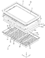
- FIG. 1 is an exploded perspective view showing a schematic configuration of a television receiver according to Embodiment 1 of the present invention.
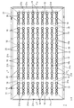
- Exploded perspective view showing schematic configuration of liquid crystal display device The top view which shows arrangement
- the bottom view which shows the arrangement structure of the chassis and each attachment component in the backlight apparatus with which a liquid crystal display device is equipped
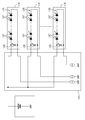
- Block diagram showing the electrical configuration of the power supply circuit of the LED substrate The block diagram showing the electric constitution which concerns on the electric power feeding circuit of the LED board which concerns on Embodiment 2 of this invention.
- FIG. 7 is an exploded perspective view showing a schematic configuration of a liquid crystal display device according to Embodiment 3 of the present invention.
- the top view which shows arrangement
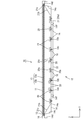
- Sectional drawing which shows the cross-sectional structure along the short side direction of a liquid crystal display device
- FIGS. 1 A first embodiment of the present invention will be described with reference to FIGS.
- the liquid crystal display device 10 is illustrated.
- a part of each drawing shows an X axis, a Y axis, and a Z axis, and each axis direction is drawn to be a direction shown in each drawing.
- the upper side shown in FIG.4 and FIG.5 be a front side, and let the lower side of the figure be a back side.
- the television receiver TV includes a liquid crystal display device 10, front and back cabinets Ca and Cb that are accommodated so as to sandwich the liquid crystal display device 10, a power source P, a tuner T, And a stand S.
- the liquid crystal display device (display device) 10 has a horizontally long (longitudinal) square shape (rectangular shape, rectangular shape) as a whole and is accommodated in a vertically placed state.
- the liquid crystal display device 10 includes a liquid crystal panel 11 that is a display panel and a backlight device (illumination device) 12 that is an external light source, which are integrated by a frame-like bezel 13 or the like. Is supposed to be retained.
- the liquid crystal panel 11 and the backlight device 12 constituting the liquid crystal display device 10 will be described sequentially.
- the liquid crystal panel (display panel) 11 has a horizontally long rectangular shape when seen in a plan view, and a pair of glass substrates are bonded together with a predetermined gap therebetween, and a liquid crystal is formed between both glass substrates. It is set as the enclosed structure.
- One glass substrate is provided with a switching element (for example, TFT) connected to a source wiring and a gate wiring orthogonal to each other, a pixel electrode connected to the switching element, an alignment film, and the like.
- a switching element for example, TFT
- the substrate is provided with a color filter and counter electrodes in which colored portions such as R (red), G (green), and B (blue) are arranged in a predetermined arrangement, and an alignment film.
- a polarizing plate is disposed on the outside of both substrates.
- the backlight device 12 includes a substantially box-shaped chassis 14 having a light emitting portion 14 b that opens on the front side (light emitting side, liquid crystal panel 11 side), and a light emitting portion 14 b of the chassis 14.
- the optical member 15 is disposed so as to cover the frame, and the frame 16 is disposed along the outer edge portion of the chassis 14 and holds the outer edge portion of the optical member 15 between the chassis 14 and the frame 16.
- the chassis 14 includes an LED 17 (Light Emitting Diode) as a light source, an LED board 18 on which the LED 17 is mounted, and a diffusion lens 19 attached to the LED board 18 at a position corresponding to the LED 17. It is done.
- LED 17 Light Emitting Diode
- the backlight device 12 is a so-called direct type in which the LEDs 17 are arranged in the chassis 14 immediately below the liquid crystal panel 11 and the optical member 15.
- an LED driving board (light source driving board) 22 that supplies driving power to the LEDs 17, a control board 23 that supplies liquid crystal driving signals to the liquid crystal panel 11;
- a power supply board 24 for supplying power to the LED drive board 22 and the control board 23 is attached.
- the chassis 14 is made of, for example, a metal plate such as an aluminum plate or an electrogalvanized steel plate (SECC). As shown in FIGS. 3 to 5, the chassis 14 has a horizontally long rectangular shape (rectangular shape, rectangular shape) like the liquid crystal panel 11. A bottom plate 14a, a side plate 14c rising from the outer end of each side (a pair of long sides and a pair of short sides) of the bottom plate 14a toward the front side (light emitting side), and outward from the rising end of each side plate 14c 14d, and is formed in a shallow box shape (substantially a dish shape) that opens toward the front side as a whole.
- the long side direction of the chassis 14 matches the X-axis direction, and the short side direction matches the Y-axis direction.
- the bottom plate 14 a in the chassis 14 is disposed on the back side of the LED substrate 18, that is, on the side opposite to the light emitting side of the LED 17.
- a frame 16 and an optical member 15 to be described below can be placed on each receiving plate 14d in the chassis 14 from the front side.
- a frame 16 is screwed to each receiving plate 14d.
- An attachment hole 14e for attaching the substrate holding member 20 is provided in the bottom plate 14a of the chassis 14 so as to open.
- a plurality of mounting holes 14e are dispersedly arranged corresponding to the mounting position of the substrate holding member 20 on the bottom plate 14a.
- the optical member 15 has a horizontally long rectangular shape when viewed in a plane, like the liquid crystal panel 11 and the chassis 14. As shown in FIGS. 4 and 5, the optical member 15 has its outer edge portion placed on the receiving plate 14 d so as to cover the light emitting portion 14 b of the chassis 14 and to be interposed between the liquid crystal panel 11 and the LED 17. Arranged.
- the optical member 15 is opposed to the LED 17 with a predetermined interval on the front side, that is, on the light emitting side.
- the optical member 15 includes a diffusion plate 15a disposed on the back side (the side opposite to the LED 17 side and the light emitting side) and an optical sheet 15b disposed on the front side (the liquid crystal panel 11 side and the light emitting side). .
- the diffusing plate 15a has a structure in which a large number of diffusing particles are dispersed in a substantially transparent resin base material having a predetermined thickness, and has a function of diffusing transmitted light.
- the optical sheet 15b has a sheet shape that is thinner than the diffusion plate 15a, and two optical sheets 15b are laminated. Specific types of the optical sheet 15b include, for example, a diffusion sheet, a lens sheet, a reflective polarizing sheet, and the like, which can be appropriately selected and used.
- the frame 16 has a frame shape along the outer peripheral edge portions of the liquid crystal panel 11 and the optical member 15. An outer edge portion of the optical member 15 can be sandwiched between the frame 16 and each receiving plate 14d (FIGS. 4 and 5).
- the frame 16 can receive the outer edge portion of the liquid crystal panel 11 from the back side, and can sandwich the outer edge portion of the liquid crystal panel 11 with the bezel 13 disposed on the front side (FIGS. 4 and 5). ).
- the LED 17 has a configuration in which an LED chip is sealed with a resin material on a substrate portion fixed to the LED substrate 18.
- the LED chip mounted on the substrate unit has one main emission wavelength, and specifically, one that emits blue light in a single color is used.
- a phosphor that emits a predetermined color by being excited by the blue light emitted from the LED chip is dispersed and blended. As a result, white light emission is possible.
- the LED 17 is a so-called top surface light emitting type in which a top surface opposite to the mounting surface with respect to the LED substrate 18 (a surface facing the optical member 15) is a light emitting surface, and its optical axis is in the Z-axis direction, That is, they are arranged so as to coincide with the direction orthogonal to the display surface of the liquid crystal panel 11 (the plate surface of the optical member 15).
- the “optical axis” refers to an axis that coincides with the traveling direction of light having the highest emission intensity among the emitted light from the LED 17.
- the LED substrate 18 has a base material that is horizontally long when viewed in plan, the long side direction coincides with the X-axis direction, and the short side direction is the Y-axis. It is accommodated while extending along the bottom plate 14a in the chassis 14 in a state matching the direction.
- the base material of the LED board 18 is made of the same metal as the chassis 14 such as an aluminum material, and a wiring pattern 18c (see FIG. 7) made of a metal film such as a copper foil is formed on the surface thereof via an insulating layer.
- the configuration is In addition, as a material used for the base material of LED board 18, insulating materials, such as a ceramic, can also be used.
- the LED 17 having the above-described configuration is surface-mounted on the surface facing the front side (the surface facing the optical member 15 side) among the plate surfaces of the base material of the LED substrate 18, and this is the mounting surface. Is done.
- a plurality of LEDs 17 are linearly arranged in parallel along the long side direction (X-axis direction) of the LED substrate 18, and are connected in series by a wiring pattern 18 c formed on the LED substrate 18.
- One LED group 25 is configured by a plurality of LEDs 17 mounted on the LED substrate 18 and connected in series by the wiring pattern 18c.
- a plurality of LEDs 17 constituting one LED group 25 are all mounted on the LED substrate 18, and a plurality of LEDs 17 constituting one LED group 25 are straddled (distributed) on the plurality of LED substrates 18. ) It will not be implemented.
- the LED boards 18 and the LED groups 25 are associated one to one, and the number of LED boards 18 accommodated in the chassis 14 and the number of LED groups 25 are the same.
- the arrangement pitch of the LEDs 17 is substantially constant, that is, it can be said that the LEDs 17 are arranged at equal intervals in the X-axis direction (row direction).
- the connector part 18a connected to the edge part of the wiring pattern 18c is formed in the both ends of the long side direction in the LED board 18, and this connector part 18a is connected to an external LED drive board 22 with an electric wire or flexible wiring.
- the LED board 18 is formed with an insertion hole 18b through the board holding member 20 at a predetermined position.
- the LED substrate 18 having the above-described configuration is arranged in parallel in the chassis 14 in a state where the long side direction and the short side direction are aligned with each other in the X-axis direction and the Y-axis direction. ing. That is, the LED board 18 and the LED 17 mounted thereon are both set in the X-axis direction (the long side direction of the chassis 14 and the LED board 18) in the chassis 14 and in the Y-axis direction (of the chassis 14 and the LED board 18).
- the short side direction is arranged in a matrix with the column direction (arranged in a matrix, planar arrangement).
- each LED 17 included in each LED group 25 can be lit with a different luminance for each LED group 25.
- adjacent connector portions 18a in the three LED boards 18 arranged in the X-axis direction are relay-connected.
- the connector 18a near the ends of the LED boards 18 at both ends may be connected to an electric wire connected to the LED drive board 22, a flexible wiring board, or the like.
- a relay wiring pattern (not shown) that is not connected to each LED 17 is formed on each of the three LED boards 18 separately from the wiring pattern 18 c that is connected in series to each LED 17. What is necessary is just to set it as the structure which connects a wiring pattern via the connector part 18a with respect to the wiring pattern 18c in the other LED board 18.
- the diffusing lens 19 is made of a synthetic resin material (for example, polycarbonate or acrylic) that is almost transparent (having high translucency) and has a refractive index higher than that of air. As shown in FIGS. 4 and 5, the diffusing lens 19 has a predetermined thickness and is formed in a substantially circular shape when viewed from above, and covers each LED 17 individually from the front side with respect to the LED substrate 18. In other words, each LED 17 is attached so as to overlap with each other when viewed in a plane.
- the diffusing lens 19 can emit light having strong directivity emitted from the LED 17 while diffusing.
- the diffusing lens 19 is disposed at a position that is substantially concentric with the LED 17 in a plan view.
- the substrate holding member 20 is made of a synthetic resin such as polycarbonate and has a white surface with excellent light reflectivity. As shown in FIGS. 4 and 5, the substrate holding member 20 is fixed to the chassis 14 by projecting toward the back side, that is, the chassis 14 side from the body portion 20 a along the plate surface of the LED substrate 18.
- the main body 20a has a substantially circular plate shape when seen in a plan view, and can hold both the LED board 18 and the reflection sheet 21 described below with the bottom plate 14a of the chassis 14.
- the fixing portion 20b can be locked to the bottom plate 14a while penetrating through the insertion hole 18b and the attachment hole 14e respectively formed corresponding to the attachment positions of the substrate holding member 20 on the LED substrate 18 and the bottom plate 14a of the chassis 14.
- a large number of the substrate holding members 20 are arranged in parallel in the surface of the LED substrate 18, and specifically, the diffusion lenses 19 (LEDs 17) adjacent to each other in the X-axis direction. It is arranged at each position.
- the pair of holding members 20 arranged on the center side of the screen is provided with a support portion 20c protruding from the main body portion 20a to the front side, as shown in FIGS.
- the support portion 20c can support the diffusion plate 15a from the back side, whereby the positional relationship in the Z-axis direction between the LED 17 and the optical member 15 can be maintained constant and the optical member 15 is not prepared. Can be controlled.
- the reflection sheet 21 is made of a synthetic resin, and the surface of the reflection sheet 21 is white with excellent light reflectivity. As shown in FIGS. 3 to 5, the reflection sheet 21 has a size that is laid over almost the entire inner surface of the chassis 14, so that the LED substrate 18 disposed in the chassis 14 is faced over the almost entire area. It is possible to cover from (light emitting side, optical member 15 side). The reflection sheet 21 can reflect light in the chassis 14 toward the front side (light emission side, optical member 15 side). The reflection sheet 21 extends along the LED substrate 18 (bottom plate 14a) and rises to the front side from each outer end of the bottom portion 21a, and a bottom portion 21a having a size that covers each LED substrate 18 in a lump.
- the bottom portion 21a of the reflection sheet 21 is arranged so as to overlap the front side surface of each LED substrate 18, that is, the mounting surface 18a of the LED 17 on the front side.
- a lens insertion hole (light source insertion hole) 21d through which each diffusion lens 19 (each LED 17) is individually inserted at a position overlapping with each diffusion lens 19 (each LED 17) in plan view is opened at the bottom 21a of the reflection sheet 21.
- a plurality of the lens insertion holes 21d are arranged in a matrix (matrix shape) in the X-axis direction and the Y-axis direction corresponding to the arrangement of the LEDs 17.
- each attachment component attached to the outside of the chassis 14 will be described in detail.
- FIGS. 4 to 6 on the back side surface of the bottom plate 14 a of the chassis 14, that is, the surface opposite to the LED substrate 18 (LED 17) side, as shown in FIG. 4 to FIG.
- a power supply board 24 is attached to each.
- the attachment base part 14f which protrudes partially toward the back side is formed in the attachment location of each attachment part in the baseplate 14a, and each attachment part is attached in the state mounted on this attachment base part 14f. It is like that.
- the LED drive substrate 22 is formed by forming a predetermined circuit pattern on a synthetic resin substrate (for example, paper phenol or glass epoxy resin) and mounting various electronic components. As shown in FIGS. 4, 6 and 7, the LED drive board 22 is connected to each LED board 18 in the chassis 14 and a power supply board 24 outside the chassis 14 via an electric wire or a flexible wiring board. It has a function of controlling the lighting / extinguishing of each LED 17 by supplying the driving voltage input from the power supply board 24 to the LEDs 17 (LED group 25) mounted on each LED board 18. . Specifically, as shown in FIG.
- the circuit pattern of the LED drive board 22 includes the positive electrode of the power supply PW of the power supply board 24 and the anode side end 18c1 of the wiring pattern 18c of the LED board 18 (LED group 25). And a negative electrode side wiring 22b connected to the cathode side end 18c2 of the wiring pattern 18c of the LED substrate 18 (LED group 25) and the ground GND.
- the positive side wiring 22a is branched from the positive side of the power source PW of the power source board 24 by the number of LED boards 18 (LED groups 25), and the branch lines are individually connected to the LED boards 18 (LED groups 25).
- the negative electrode side wiring 22b is provided by the number of LED boards 18 (LED group 25).
- the positive electrode side wiring 22a and the negative electrode side wiring 22b are provided in the same number as the number of the LED boards 18 (LED groups 25).
- the LED drive board 22 is arranged near one end portion in the long side direction of the bottom plate 14a of the chassis 14, and is attached to the mounting base portion 14f formed there by a screw or the like. It is attached.
- the control board 23 has a predetermined circuit pattern (not shown) formed on a synthetic resin board (for example, paper phenol or glass epoxy resin), and various input signals such as a TV signal from the tuner T. Is converted into a liquid crystal driving signal, and the converted liquid crystal driving signal is supplied to the liquid crystal panel 11. As shown in FIGS. 4 and 6, the control board 23 is disposed at a substantially central position in the long side direction and at a lower position shown in FIG. 6 in the short side direction of the bottom plate 14 a of the chassis 14. It is attached to a mounting base portion 14f formed there by a screw or the like.
- a synthetic resin board for example, paper phenol or glass epoxy resin
- the power supply board 24 is a power supply source that supplies power to the LED drive board 22, the control board 23, and the like. As shown in FIGS. 4 and 6, the power supply board 24 is disposed at a substantially central position in the long side direction and at an upper position shown in FIG. 6 in the short side direction of the bottom plate 14 a of the chassis 14. It is attached to a mounting base portion 14f formed there by a screw or the like.
- the above-described LED drive board 22 is provided with a variable resistor 26 connected in parallel to each LED group 25 of each LED board 18.
- the variable resistor 26 can change its own resistance value, and can control the amount of current supplied to the LED group 25 that is a load connected in parallel.
- the variable resistor 26 has a pair of terminal portions (not shown). In the circuit pattern of the LED drive board 22, one terminal portion is on the positive electrode side wiring 22a and the other terminal portion is on the negative electrode side. By being connected to each of the wirings 22b, they are connected in parallel to the LED group 25 connected to the positive electrode side wiring 22a and the negative electrode side wiring 22b.
- the resistance value of the variable resistor 26 is increased, the current value of the current that flows through the variable resistor 26 decreases, so that the current value of the current that flows through the LED group 25 increases, and conversely, if the resistance value is decreased. Since the current value of the current flowing through the variable resistor 26 increases, the current value of the current flowing through the LED group 25 decreases.
- variable resistors 26 as the LED boards 18 and LED groups 25 are provided, and are individually connected in parallel to the LED groups 25. Therefore, the amount of current supplied to each LED group 25 can be individually controlled by adjusting the resistance value of each variable resistor 26 prepared individually for each LED group 25. Thereby, it is possible to make the luminance uniform among the LED groups 25.
- variable resistor 26 is mounted together with other electronic components on the back surface of the LED drive board 22, that is, the surface opposite to the bottom plate 14 a side of the chassis 14.
- the variable resistor 26 has an operation unit (not shown) that can be operated from the outside.
- the variable resistor 26 operates by operating the operation unit from the back side of the LED drive board 22.
- the value can be changed. Therefore, when changing the resistance value of the variable resistor 26, the chassis 14 is exposed in the vertical direction in which the LED drive board 22 and the variable resistor 26 are exposed (the posture in which the light emitting portion 14b is downward in the vertical direction). However, it is preferable to operate the operation part of the variable resistor 26.
- current control circuits 27 which are constant current sources, are individually connected to the negative-side wirings 22b.
- the current control circuit 27 can keep the current value flowing through the negative electrode side wiring 22b constant, and thereby the current value flowing through the LED group 25 and the current value flowing through the variable resistor 26 are determined. It is possible to keep the total current value added together constant. Therefore, by adjusting the resistance value of the variable resistor 26, the current value of the current flowing through the LED group 25 can be uniquely controlled.
- This embodiment has the structure as described above, and its operation will be described next.
- the separately manufactured liquid crystal panel 11, backlight device 12, bezel 13 and the like are assembled.
- the manufacturing procedure of the backlight device 12 will be described mainly with respect to the manufacturing procedure of the liquid crystal display device 10.
- each LED substrate 18 on which the LEDs 17 are mounted in the chassis 14 is accommodated from the front side, and then a reflective sheet 21 is laid, and then the substrate holding member 20 is attached, whereby each LED substrate 18 is attached.
- the reflection sheet 21 is held attached to the chassis 14.
- the optical members 15 are stacked and arranged so as to cover the light emitting portion 14b of the chassis 14, and then the frame 16 is attached to hold the optical member 15, and the front-side components of the backlight device 12 Assembly is complete. Then, by assembling the liquid crystal panel 11 and the bezel 13, the assembly of the front-side components in the liquid crystal display device 10 is completed.
- each mounting part on the back side of the backlight device 12 is assembled. Place the LED drive board 22, the control board 23, and the power supply board 24 on each mounting base part 14f, and tighten screws or the like, with the chassis 14 in a posture in which the back side surface of the bottom plate 14a is upward in the vertical direction. As a result, each attachment component is fixed in the attached state. At this time, it is possible to adjust the resistance value of each variable resistor 26 by operating the operation part of each variable resistor 26 mounted on the back side surface of the LED drive board 22 (FIGS. 4 and 6). See).
- each LED group 25 of each LED board 18 may have different current luminance characteristics due to individual differences in manufacturing, and in that case, the resistance value of each variable resistor 26 is adjusted as described above. As a result, it is possible to make it difficult for a difference in luminance between the LED groups 25 to occur.
- each LED 17 mounted on each LED board 18 via the LED to turn it on and various signals for liquid crystal display are supplied from the control board 23 to the liquid crystal panel 11.
- the light emitted from each LED 17 is incident on the incident surface (the surface facing the LED 17) of the diffusion lens 19, and then diffused and emitted from the exit surface (the surface facing the optical member 15) while being refracted at a wide angle.
- the optical member 15 is directly irradiated without unevenness, and after being reflected by the reflection sheet 21, the optical member 15 is irradiated.
- the light irradiated to the optical member 15 is given a predetermined optical action (such as a diffusing action or a light collecting action) in the process of passing through the optical member 15.
- a predetermined image is displayed on the display surface of the liquid crystal panel 11 by irradiating the liquid crystal panel 11 with light transmitted through the optical member 15.
- the LED 17 when the liquid crystal display device 10 is used, contact failure occurs in the connector portion 18a of the LED substrate 18, disconnection occurs in the wiring pattern, or contact failure occurs in the mounting location of the mounted LED 17. There is a risk that the LED 17 may have a problem such as a lighting failure. In that case, it is necessary to perform repairs such as replacing the LED board 18 in which a problem has occurred with a new LED board 18.
- the LED 17 generally has a current luminance characteristic that deteriorates with time, and even if the current value to be applied remains unchanged, the luminance tends to decrease as the cumulative lighting time increases.
- the current luminance characteristics are different between each LED 17 constituting the LED group 25 of the new LED board 18 installed in accordance with the above-described repair and each LED 17 constituting the LED group 25 of the existing LED board 18. ing.
- the former luminance is obtained.
- the luminance becomes relatively higher than the latter luminance, which may cause uneven luminance.
- variable resistor 26 is connected in parallel to the LED group 25 of the LED board 18.
- the difference in luminance that can be generated between each LED 17 forming the LED group 25 included in the new LED substrate 18 and each LED 17 included in the LED group 25 included in the existing LED substrate 18 can be reduced.
- the resistance value of the variable resistor 26 connected in parallel to the LED group 25 included in the new replaced LED board 18 is changed, and the LED group 25 included in another existing LED board 18 is connected in parallel.
- the resistance value of each variable resistor 26 is relatively lower.
- the LED group 25 included in the new LED board 18 is adjusted so as to suppress the brightness, and the LED group 25 included in the existing LED board 18 is not adjusted to increase the brightness ( Since the brightness is not changed), it is possible to obtain an effect that heat generation from each LED 17 can be suppressed.
- a new LED that is replaced by changing the resistance value of each variable resistor 26 connected in parallel to the LED group 25 included in each LED board 18 that is not replaced is replaced. You may make it make it relatively higher than the resistance value in the variable resistance 26 connected in parallel with LED group 25 which the board
- variable resistors 26 are provided on the LED drive board 22 and are individually connected in parallel to each LED group 25. Therefore, which of the variable resistors 26 is arranged in the backlight device 12. Even when a problem occurs in the LED board 18, it is possible to easily and surely cope with it, and it is possible to make the luminance uniform among the LED groups 25 of all the LED boards 18. In addition, since all the variable resistors 26 are centrally arranged on the LED drive substrate 22, the workability of performing the work of changing the resistance value is excellent.
- the LED board 18 and the LED group 25 are associated one-to-one, and the LEDs 17 forming one LED group 25 are not arranged across the plurality of LED boards 18, so that the LED group 25 in which a problem has occurred is generated. Therefore, it is only necessary to replace the LED board 18 having an LED, and it is not necessary to replace even the LED board 18 including the LED group 25 in which no problem occurs. Therefore, it is suitable for cost reduction and the workability is excellent.
- each variable resistor 26 mounted on the back side surface of the LED drive board 22 while the chassis 14 is in a posture in which the back side surface of the bottom plate 14a is vertically upward.
- the resistance value of each variable resistor 26 is adjusted (see FIGS. 4 and 6).
- the current value of the current flowing through each LED group 25 can be set to an appropriate value, and the brightness can be adjusted to be uniform among the LED groups 25.
- the variable resistor 26 provided on the LED drive board 22 attached to the back surface of the chassis 14 may be operated. If the variable resistor is provided on the LED board 18, Compared with the need to remove components such as 16, the optical member 15 and the reflective sheet 21, the workability is excellent.
- the backlight device (illumination device) 12 of the present embodiment includes a plurality of LED groups (light source groups) 25 and a plurality of LED groups 25 formed by connecting a plurality of LEDs (light sources) 17 in series.
- substrate (light source drive part) 22 to drive and the variable resistance 26 connected in parallel with respect to at least any one LED group 25 in the some LED group 25 are provided.
- Each LED 17 constituting each LED group 25 can be turned on by driving the plurality of LED groups 25 by the LED drive board 22.
- the existing LED group 25 that does not need to be replaced has a current luminance characteristic that has changed over time and is different from the current luminance characteristic of the new LED group 25 that has been replaced.
- driving by supplying current there is a risk that a difference in luminance occurs. Therefore, by changing the resistance value of the variable resistor 26, the amount of current supplied to the plurality of LEDs 17 constituting the LED group 25 to which the variable resistor 26 is connected in parallel can be adjusted. The difference in brightness that can occur between the LED group 25 and the existing LED group 25 can be reduced. Thereby, luminance unevenness hardly occurs in the emitted light from the backlight device 12.
- variable resistors 26 are provided in the same number as the plurality of LED groups 25 and are individually connected in parallel to the plurality of LED groups 25. In this way, for example, by changing the resistance value of the variable resistor 26 connected in parallel with respect to at least one of the replaced new LED group 25 and the existing LED group 25, all the LED groups 25 can be changed. It is possible to make the luminance uniform between the two.
- the same number of LED boards (light source boards) 18 on which a plurality of LEDs 17 constituting one LED group 25 are mounted are provided.
- the cost can be reduced compared to the need to replace a plurality of LED substrates together.
- it is suitable for improving the workability and is excellent in workability.
- the LED board 18 on which a plurality of LEDs 17 constituting the LED group 25 are mounted is provided, and the variable resistor 26 is provided on the LED drive board 22.
- the LED driving board 22 is easier to secure a space than the LED board 18 on which the plurality of LEDs 17 constituting the LED group 25 are mounted.
- the LED substrate 18 can be reduced in size, and a general-purpose product without the variable resistor 26 can be used as the LED substrate 18, which is excellent in terms of cost.
- a plurality of variable resistors 26 are provided on the LED drive board 22 so that each of the plurality of LED groups 25 is individually connected in parallel. In this way, when the work of changing the resistance value in the variable resistor 26 is performed, all of the plurality of variable resistors 26 individually connected in parallel to all of the plurality of LED groups 25 are all on the LED drive board 22. Since they are provided in a centralized manner, workability is improved.
- a chassis 14 in which the LED substrate 18 is accommodated and a light emitting portion 14b that emits light and an optical member 15 that is arranged to cover the light emitting portion 14b are provided.
- the chassis 14 is disposed on the surface opposite to the light emitting portion 14b side. In this way, the resistance value of the variable resistor 26 is changed in order to adjust the amount of current supplied to the plurality of LEDs 17 constituting the LED group 25 separately from the operation of replacing the defective LED group 25. Therefore, it is not necessary to remove the optical member 15 arranged so as to cover the light emitting portion 14b in the chassis 14, so that the workability is excellent.
- a current control circuit 27 that controls the current value of the current flowing through the LED group 25 and the variable resistor 26 connected in parallel to the LED group 25 to be constant is provided. In this way, by adjusting the resistance value of the variable resistor 26, the current value flowing through the LED group 25 can be appropriately controlled.
- the LED 17 emits white light. In this way, it is possible to suitably prevent a brightness difference from occurring in the white light emitted from each LED 17 constituting the plurality of LED groups 25.
- the light source is the LED 17. In this way, high brightness and low power consumption can be achieved.
- the variable resistor 126 is mounted on the LED substrate 118 as shown in FIG.
- the variable resistors 126 are provided in the same number as the LED boards 118, are individually mounted on all the LED boards 118, and are individually connected in parallel to all the LED groups 125. Since the variable resistor 126 is provided integrally with the LED board 118, it is possible to simultaneously change the resistance value of the variable resistor 126 when the LED board 118 is replaced. . Therefore, in this embodiment, the operation of changing the resistance value of the variable resistor 26 as in the case of providing the variable resistor 26 on the LED drive board 22 as in the first embodiment (see FIGS. 6 and 7). There is no need to perform the work of inverting the chassis 14 when performing the operation, and the workability is further improved.
- the LED substrate 118 on which the plurality of LEDs 117 forming the LED group 125 are mounted is provided, and the variable resistor 126 is provided on the LED substrate 118.
- the work for replacing the LED board 118 having the defective LED group 125 is performed, the work for changing the resistance value of the variable resistor 126 provided on the LED board 118 can be performed. Excellent workability.
- the chassis 14 for housing the LED board 118 is provided, and the LED driving board 122 is disposed on the surface of the chassis 14 opposite to the surface on the LED board 118 side.
- the variable resistance 26 is provided on the LED drive substrate 22 as in the first embodiment.
- the chassis 14 needs to be inverted, but according to the present embodiment, this need does not occur, and the workability is excellent.
- FIGS. 3 A third embodiment of the present invention will be described with reference to FIGS.
- the third embodiment shows a case where the backlight device 212 is changed to an edge light type.
- the liquid crystal display device 210 has a configuration in which a liquid crystal panel 211 and an edge light type backlight device 212 are integrated by a bezel 213 or the like. Note that the configuration of the liquid crystal panel 211 is the same as that of the first embodiment, and a duplicate description thereof is omitted. Hereinafter, the configuration of the edge light type backlight device 212 will be described.
- the backlight device 212 has a substantially box-shaped chassis 214 having a light emitting portion 214 b that opens toward the front side (the liquid crystal panel 211 side), and covers the opening of the chassis 214. And a plurality of optical members 215 arranged. Furthermore, in the chassis 214, an LED 217 (Light Emitting Diode) as a light source, an LED substrate 218 on which the LED 217 is mounted, and light from the LED 217 are guided to the optical member 215 (liquid crystal panel 211). And a frame 216 for holding the light guide plate 28 from the front side.
- LED 217 Light Emitting Diode
- the backlight device 212 includes LED substrates 218 having LEDs 217 at both ends on the long side thereof, and a so-called light guide plate 28 disposed at the center between the LED substrates 218. It is an edge light type (side light type). Thus, since the backlight device 212 according to this embodiment is an edge light type, the diffusing lens 19, the substrate holding member 20, and the reflection sheet used in the direct type backlight device 12 shown in the first embodiment are used. 21 etc. are not provided. Next, each component of the backlight device 212 will be described in detail.
- the chassis 214 is made of metal and includes a bottom plate 214a having a horizontally long rectangular shape as in the liquid crystal panel 211, and side plates 214c rising from the outer ends of the respective sides of the bottom plate 214a. As a whole, it has a shallow, generally box shape that opens toward the front side.
- the chassis 214 (bottom plate 214a) has a long side direction that coincides with the X-axis direction (horizontal direction) and a short side direction that coincides with the Y-axis direction (vertical direction).
- the frame 216 and the bezel 213 can be screwed to the side plate 214c.
- the optical member 215 is the same as that of the first embodiment except that three optical sheets 215b are provided.
- the frame 216 is formed in a frame shape (frame shape) extending along the outer peripheral end of the light guide plate 28, and the outer peripheral end of the light guide plate 28 extends from the front side over almost the entire periphery. It is possible to hold down.
- the frame 216 is made of a synthetic resin and has a light shielding property by having a surface with, for example, a black color.
- a first reflection sheet 29 that reflects light is attached to the back surface of both long side portions of the frame 216, that is, the surface facing the light guide plate 28 and the LED substrate 218 (LED 217). It has been.
- the first reflection sheet 29 has a size that extends over almost the entire length of the long side portion of the frame 216, and is in direct contact with the end of the light guide plate 28 on the LED 217 side and the end of the light guide plate 28. And the LED substrate 218 are collectively covered from the front side. Further, the frame 216 can receive the outer peripheral end of the liquid crystal panel 211 from the back side.
- the LED board 218 has a long and narrow plate shape extending along the long side direction of the chassis 214 (X-axis direction, the longitudinal direction of the light incident surface 28b of the light guide plate 28), and its main plate.
- the surface is accommodated in the chassis 214 in a posture parallel to the X-axis direction and the Z-axis direction, that is, in a posture orthogonal to the liquid crystal panel 211 and the light guide plate 28 (optical member 215).
- a pair of LED substrates 218 are arranged corresponding to both ends on the long side in the chassis 214, and are attached to the inner surfaces of both side plates 214b on the long side.
- the LED 217 having the above-described configuration is mounted on the main plate surface of the LED substrate 218 and on the inner side, that is, the surface facing the light guide plate 28 side (the surface facing the light guide plate 28).
- a plurality of LEDs 217 are arranged in a line (linearly) in parallel along the length direction (X-axis direction) on the mounting surface of the LED substrate 218. Therefore, it can be said that a plurality of LEDs 217 are arranged in parallel along the long side direction at both ends on the long side of the backlight device 212.
- a plurality of LEDs 217 mounted on each LED substrate 218 are connected in series by a wiring pattern (not shown), and one LED group 25 is configured by these LEDs 217. Since the pair of LED substrates 218 are housed in the chassis 214 in a posture in which the mounting surfaces of the LEDs 217 are opposed to each other, the light emitting surfaces of the LEDs 217 mounted on the LED substrates 218 are opposed to each other, The optical axis of each LED 217 substantially coincides with the Y-axis direction.
- the light guide plate 28 is made of a synthetic resin material (for example, acrylic) having a refractive index sufficiently higher than that of air and almost transparent (excellent translucency). As shown in FIG. 9, the light guide plate 28 has a horizontally long rectangular shape when viewed in a plane, like the liquid crystal panel 211 and the chassis 214, and the long side direction is the X axis direction and the short side direction is the Y axis. Each direction matches.
- the light guide plate 28 is disposed in the chassis 214 at a position directly below the liquid crystal panel 211 and the optical member 215, and is sandwiched between the pair of LED substrates 218 disposed at both ends of the long side of the chassis 214 in the Y-axis direction. It is arranged in the form.
- the alignment direction of the LED 217 (LED substrate 218) and the light guide plate 28 coincides with the Y-axis direction, whereas the alignment direction of the optical member 215 (liquid crystal panel 211) and the light guide plate 28 matches the Z-axis direction. It is assumed that both directions are orthogonal to each other.
- the light guide plate 28 introduces the light emitted from the LED 217 toward the Y-axis direction, and raises and emits the light toward the optical member 215 side (Z-axis direction) while propagating the light inside.
- the surface facing the front side is a light emitting surface 28 a that emits internal light toward the optical member 215 and the liquid crystal panel 211.
- a light emitting surface 28 a that emits internal light toward the optical member 215 and the liquid crystal panel 211.
- both end surfaces on the long side that are long along the X-axis direction are opposed to the LED 217 (LED substrate 218), respectively, with a predetermined interval therebetween.
- the light incident surface 28b is a surface that is parallel to the X-axis direction and the Z-axis direction, and is a surface that is substantially orthogonal to the light emitting surface 28a.
- a second reflection sheet 30 that reflects the light in the light guide plate 28 and can be raised to the front side is provided on the surface 28c of the light guide plate 28 opposite to the light exit surface 28a so as to cover the entire area. ing.
- the second reflection sheet 30 is extended to a range where it overlaps with the LED board 218 (LED 217) in a plan view, and the LED board 218 (LED 217) is sandwiched between the first reflection sheet 29 on the front side. Has been. Thereby, the light from the LED 217 can be efficiently incident on the light incident surface 28b by repeatedly reflecting between the reflecting sheets 29 and 30.
- At least one of the light exit surface 28a and the opposite surface 28c of the light guide plate 28 has a reflection part (not shown) for reflecting internal light or a scattering part (not shown) for scattering internal light.
- a reflection part for reflecting internal light
- a scattering part for scattering internal light.
- the backlight device 212 configured as described above, by providing the variable resistor 26 connected in parallel to each LED group 225 on the LED drive board 22 as in the first embodiment (see FIG. 7).
- the brightness difference between the LED groups 225 can be alleviated to prevent uneven brightness from occurring in the light emitted from the backlight device 212.
- Embodiment 1 the power supply configuration in which a plurality of LED boards arranged in the X-axis direction are connected to each other by a connector portion and the LED boards at both ends are connected to the LED drive board is shown.
- a power feeding configuration in which an electric wire or a flexible wiring board connected to the LED driving board is individually connected to each LED board.
- the LED group and the LED substrate are shown in a one-to-one correspondence.
- the LEDs constituting one LED group straddle a plurality of LED substrates. It is also possible to adopt a configuration (a configuration in which LEDs constituting a plurality of LED groups are mixed on one LED substrate).
- variable resistors are individually connected in parallel to all the LED groups.
- a configuration in which the number of variable resistors is smaller than the number of LED groups and the variable resistors are connected in parallel to the LED groups and the variable resistors are not connected may be mixed.
- a variable resistor is connected in parallel only to such an LED group.
- a variable resistor may not be connected for an LED group that is predicted to have a low possibility of replacement.
- the LED drive board and the LED board are directly connected to each other.
- the relay board for relaying these between the LED drive board and the LED board can also be applied to a configuration in which a gap is interposed. In that case, it is possible to adopt a configuration in which a variable resistor is provided on the relay substrate.
- the current value supplied to each LED substrate and the luminance of the LEDs constituting the LED group can be individually varied, for example, when a bright part and a dark part are mixed in an image displayed on the liquid crystal panel, So-called local dimming is achieved by relatively high luminance for the LEDs forming the LED group that irradiates light in the bright part and relatively low luminance or non-lighting for the LED that irradiates the light in the dark part. Control can be performed.
- Embodiment 1 a configuration in which a horizontally long LED substrate is arranged in parallel in a matrix along the long side direction and the short side direction of the chassis is shown. It is also possible to adopt a configuration in which a plurality of LED substrates are arranged in parallel in a matrix along the long side direction and short side direction of the chassis.
- a vertically long LED board it is possible to make the long side dimension the same as the short side dimension of the bottom plate of the chassis and to arrange a plurality of LED boards in parallel in the long side direction of the chassis. It is.
- Embodiment 1 a configuration in which a horizontally long LED substrate is arranged in parallel in a matrix along the long side direction and the short side direction of the chassis has been shown. It is also possible to adopt a configuration in which the long side dimension of the LED substrate is approximately the same as the long side dimension of the bottom plate of the chassis, and a plurality of the LED substrates are arranged in parallel in the short side direction of the chassis.
- the diffuser lens is disposed on the light emitting side of the LED.
- the present invention can also be applied to a direct type backlight device in which such a diffuser lens is omitted. .
- a pair of LED substrates are arranged at the ends of both long sides of the light guide plate.
- the LED substrates are both short sides of the light guide plate. What is arranged in a pair at the end portion on the side is also included in the present invention.
- LED substrates (10) In addition to the above (9), a pair of LED substrates (LEDs) arranged with respect to the ends of both long sides and short sides of the light guide plate, and conversely LED substrates (LEDs).
- the present invention includes one in which only one long side or one short side of the light guide plate is disposed at the end.
- the number of LED boards accommodated in the chassis that is, the number of LED groups can be changed as appropriate.
- the specific number of LEDs mounted on the LED substrate that is, the number of LEDs included in one LED group can be changed as appropriate.
- an LED that emits white light is used as a light source.
- three types of LEDs that emit red light, green light, and blue light in a single color can be used. is there.
- an LED is used as a light source, but other light sources such as an organic EL can be used.
- the liquid crystal panel and the chassis are illustrated in a vertically placed state in which the short side direction coincides with the vertical direction.
- the liquid crystal panel and the chassis have the long side direction in the vertical direction.
- Those that are in a vertically placed state matched with are also included in the present invention.
- a TFT is used as a switching element of a liquid crystal display device.
- the present invention can also be applied to a liquid crystal display device using a switching element other than TFT (for example, a thin film diode (TFD)).
- a switching element other than TFT for example, a thin film diode (TFD)
- the present invention can also be applied to a liquid crystal display device for monochrome display.
- the liquid crystal display device using the liquid crystal panel as the display panel has been exemplified.
- the present invention can also be applied to display devices using other types of display panels.
- the television receiver provided with the tuner is exemplified.
- the present invention can also be applied to a display device that does not include the tuner.
Landscapes
- Physics & Mathematics (AREA)
- Nonlinear Science (AREA)
- Mathematical Physics (AREA)
- Chemical & Material Sciences (AREA)
- Crystallography & Structural Chemistry (AREA)
- General Physics & Mathematics (AREA)
- Optics & Photonics (AREA)
- Planar Illumination Modules (AREA)
Abstract
本発明に係るバックライト装置(照明装置)12は、複数のLED(光源)17を直列接続してなる、複数のLED群(光源群)25と、複数のLED群25を駆動するLED駆動基板(光源駆動部)22と、複数のLED群25における少なくともいずれか1つのLED群25に対して並列接続される可変抵抗26と、を備える。LED群25をなす複数のLED17は、LED基板(光源基板)18に実装されている。
Description
本発明は、照明装置、表示装置、及びテレビ受信装置に関する。
例えば、液晶テレビなどの液晶表示装置に用いる液晶パネルは、自発光しないため、別途に照明装置としてバックライト装置を必要としている。このバックライト装置は、液晶パネルの裏側(表示面とは反対側)に設置されるようになっており、液晶パネル側の面が開口したシャーシと、シャーシ内に収容される光源と、光源と対向するようシャーシの開口部を覆う形で配されて光源が発する光を効率的に液晶パネル側へ放出させるための光学部材(拡散シート等)とを備える。上記したバックライト装置の構成部品のうち、光源として例えばLEDを用いる場合があり、その場合には、シャーシ内にLEDを実装したLED基板を収容することになる。
なお、光源としてLEDを用いたバックライト装置の一例として下記特許文献1に記載されたものが知られている。
なお、光源としてLEDを用いたバックライト装置の一例として下記特許文献1に記載されたものが知られている。
(発明が解決しようとする課題)
上記のようなバックライト装置においては、複数のLEDを実装したLED基板を複数枚使用することがあるが、使用に伴っていずれかのLED基板に実装されたLEDに点灯不良などの不具合が生じた場合には、不具合が生じたLEDを有するLED基板を、新たなLED基板に交換する、といった修理を行う必要がある。ここで、一般的にLEDは、電流輝度特性が経時的に劣化するものであり、付与する電流値が不変であっても、累積点灯時間の増加に伴って輝度が低下する傾向にある。このため、上記した修理に伴って設置された新たなLED基板のLEDと、既設のLED基板のLEDとでは、電流輝度特性が異なることとなって、両者間に輝度差が生じるおそれがあり、それに起因して輝度ムラが発生する可能性があった。
上記のようなバックライト装置においては、複数のLEDを実装したLED基板を複数枚使用することがあるが、使用に伴っていずれかのLED基板に実装されたLEDに点灯不良などの不具合が生じた場合には、不具合が生じたLEDを有するLED基板を、新たなLED基板に交換する、といった修理を行う必要がある。ここで、一般的にLEDは、電流輝度特性が経時的に劣化するものであり、付与する電流値が不変であっても、累積点灯時間の増加に伴って輝度が低下する傾向にある。このため、上記した修理に伴って設置された新たなLED基板のLEDと、既設のLED基板のLEDとでは、電流輝度特性が異なることとなって、両者間に輝度差が生じるおそれがあり、それに起因して輝度ムラが発生する可能性があった。
本発明は上記のような事情に基づいて完成されたものであって、輝度ムラを抑制することを目的とする。
(課題を解決するための手段)
本発明の照明装置は、複数の光源を直列接続してなる、複数の光源群と、複数の前記光源群を駆動する光源駆動部と、複数の前記光源群における少なくともいずれか1つの前記光源群に対して並列接続される可変抵抗と、を備える。
本発明の照明装置は、複数の光源を直列接続してなる、複数の光源群と、複数の前記光源群を駆動する光源駆動部と、複数の前記光源群における少なくともいずれか1つの前記光源群に対して並列接続される可変抵抗と、を備える。
光源駆動部によって複数の光源群を駆動することで、各光源群を構成する各光源を点灯させることができる。ここで、複数の光源群のいずれかに不具合が生じた場合には、その光源群を新たなものに交換する必要がある。このとき、交換を要さない既設の光源群は、電流輝度特性が経時変化していて交換した新たな光源群に係る電流輝度特性とは異なっているため、仮にこれらに同じ電流値の電流を供給して駆動すると、輝度差が生じるおそれがある。そこで、可変抵抗における抵抗値を変更することで、その可変抵抗が並列接続された光源群を構成する複数の光源に供給される電流量を調整することができるので、交換した新たな光源群と既設の光源群との間に生じ得る輝度差を緩和することができる。これにより、当該照明装置における出射光に輝度ムラが生じ難くなる。
本発明の実施態様として、次の構成が好ましい。
(1)前記可変抵抗は、複数の前記光源群と同数備えられるとともに、複数の前記光源群に対してそれぞれ個別に並列接続されている。このようにすれば、例えば、交換した新たな光源群と既設の光源群との少なくともいずれか一方について、並列接続された可変抵抗における抵抗値を変更することで、全ての光源群間における輝度の均一化を図ることができる。
(1)前記可変抵抗は、複数の前記光源群と同数備えられるとともに、複数の前記光源群に対してそれぞれ個別に並列接続されている。このようにすれば、例えば、交換した新たな光源群と既設の光源群との少なくともいずれか一方について、並列接続された可変抵抗における抵抗値を変更することで、全ての光源群間における輝度の均一化を図ることができる。
(2)1つの前記光源群をなす複数の前記光源が全て実装される光源基板が、複数の前記光源群と同数備えられている。このようにすれば、所定の光源群に不具合が生じた場合、その不具合が生じた光源群が実装された光源基板のみを交換すればよい。従って、仮に1つの光源群をなす複数の光源が複数の光源基板に跨って配された構成とした場合には複数の光源基板をまとめて交換する必要があるのと比べると、低コスト化を図る上で好適であり、また作業性にも優れる。
(3)前記光源群をなす複数の前記光源が実装される光源基板が備えられており、前記可変抵抗は、前記光源駆動部に設けられている。このようにすれば、光源駆動部は、光源群をなす複数の光源が実装される光源基板に比べると、スペースを確保するのが容易であるから、仮に光源基板に可変抵抗を設けた場合に比べると、光源基板を小型にすることができ、また光源基板として可変抵抗を有さない汎用品を用いることが可能となってコスト面でも優れる。
(4)前記可変抵抗は、複数の前記光源群の全てに対してそれぞれ個別に並列接続されるよう、複数が前記光源駆動部に設けられている。このようにすれば、可変抵抗における抵抗値を変更する作業を行う際、複数の前記光源群の全てに対してそれぞれ個別に並列接続される複数の可変抵抗が全てが光源駆動部に集約して設けられているので、作業性が良好なものとなる。
(5)光を出射させる光出射部を有するとともに前記光源基板が収容されるシャーシと、前記光出射部を覆う形で配される光学部材とが備えられており、前記光源駆動部は、前記シャーシのうち前記光出射部側とは反対側の面に配されている。このようにすれば、不具合が生じた光源群を交換する作業とは別途に、光源群を構成する複数の光源に供給される電流量を調整するために可変抵抗における抵抗値を変更する作業を行う必要があった場合、シャーシにおける光出射部を覆う形で配される光学部材を取り外す必要がなく、もって作業性に優れる。
(6)前記光源群をなす複数の前記光源が実装される光源基板が備えられており、前記可変抵抗は、前記光源基板に設けられている。このようにすれば、不具合が生じた光源群を有する光源基板を交換する作業を行う際に、光源基板に設けられた可変抵抗における抵抗値を変更する作業を行うことができるから、作業性に優れる。
(7)前記光源基板を収容するシャーシが備えられており、前記光源駆動部は、前記シャーシのうち前記光源基板側の面とは反対側の面に配されている。このようにすれば、光源基板の交換作業を行う際に、可変抵抗における抵抗値を変更する作業を行うとき、仮に光源駆動部に可変抵抗を設けた場合にはシャーシを反転させる必要が生じるものの、本発明によればその必要が生じることがなく、もって作業性により優れる。
(8)前記光源群とその光源群に並列接続された前記可変抵抗とに流れる電流の電流値が一定になるよう制御する電流制御回路が備えられている。このようにすれば、可変抵抗の抵抗値を調整することで、光源群に流れる電流値を適切に制御することができる。
(9)前記光源は、白色光を発するものとされる。このようにすれば、複数の光源群を構成する各光源が発する白色光に輝度差が生じるのが好適に防がれる。
(10)前記光源は、LEDとされる。このようにすれば、高輝度化及び低消費電力化などを図ることができる。
次に、上記課題を解決するために、本発明の表示装置は、上記記載の照明装置と、前記照明装置からの光を利用して表示を行う表示パネルとを備える。
このような表示装置によると、表示パネルに対して光を供給する照明装置が、輝度ムラが生じ難いものであるため、表示品質の優れた表示を実現することが可能となる。
前記表示パネルとしては液晶パネルを例示することができる。このような表示装置は液晶表示装置として、種々の用途、例えばテレビやパソコンのディスプレイ等に適用でき、特に大型画面用として好適である。
(発明の効果)
本発明によれば、輝度ムラを抑制することができる。
本発明によれば、輝度ムラを抑制することができる。
<実施形態1>
本発明の実施形態1を図1から図7によって説明する。本実施形態では、液晶表示装置10について例示する。なお、各図面の一部にはX軸、Y軸及びZ軸を示しており、各軸方向が各図面で示した方向となるように描かれている。また、図4及び図5に示す上側を表側とし、同図下側を裏側とする。
本発明の実施形態1を図1から図7によって説明する。本実施形態では、液晶表示装置10について例示する。なお、各図面の一部にはX軸、Y軸及びZ軸を示しており、各軸方向が各図面で示した方向となるように描かれている。また、図4及び図5に示す上側を表側とし、同図下側を裏側とする。
本実施形態に係るテレビ受信装置TVは、図1に示すように、液晶表示装置10と、当該液晶表示装置10を挟むようにして収容する表裏両キャビネットCa,Cbと、電源Pと、チューナーTと、スタンドSとを備えて構成される。液晶表示装置(表示装置)10は、全体として横長(長手)の方形状(矩形状、長方形状)をなし、縦置き状態で収容されている。この液晶表示装置10は、図2に示すように、表示パネルである液晶パネル11と、外部光源であるバックライト装置(照明装置)12とを備え、これらが枠状のベゼル13などにより一体的に保持されるようになっている。
次に、液晶表示装置10を構成する液晶パネル11及びバックライト装置12について順次に説明する。このうち、液晶パネル(表示パネル)11は、平面に視て横長な方形状をなしており、一対のガラス基板が所定のギャップを隔てた状態で貼り合わせられるとともに、両ガラス基板間に液晶が封入された構成とされる。一方のガラス基板には、互いに直交するソース配線とゲート配線とに接続されたスイッチング素子(例えばTFT)と、そのスイッチング素子に接続された画素電極、さらには配向膜等が設けられ、他方のガラス基板には、R(赤色),G(緑色),B(青色)等の各着色部が所定配列で配置されたカラーフィルタや対向電極、さらには配向膜等が設けられている。なお、両基板の外側には偏光板が配されている。
続いて、バックライト装置12について詳しく説明する。バックライト装置12は、図2に示すように、表側(光出射側、液晶パネル11側)に開口する光出射部14bを有した略箱型をなすシャーシ14と、シャーシ14の光出射部14bを覆うようにして配される光学部材15と、シャーシ14の外縁部に沿って配され光学部材15の外縁部をシャーシ14との間で挟んで保持するフレーム16とを備える。さらに、シャーシ14内には、光源であるLED17(Light Emitting Diode:発光ダイオード)と、LED17が実装されたLED基板18と、LED基板18においてLED17に対応した位置に取り付けられる拡散レンズ19とが備えられる。その上、シャーシ14内には、LED基板18をシャーシ14との間で保持することが可能な基板保持部材20と、シャーシ14内の光を表側(光出射側、光学部材15側)に向けて反射させる反射シート21とが備えられる。このように、本実施形態に係るバックライト装置12は、シャーシ14内において液晶パネル11及び光学部材15の直下位置にLED17が配された、いわゆる直下型とされる。一方、シャーシ14外には、図6に示すように、LED17に駆動電力を供給するLED駆動基板(光源駆動基板)22と、液晶パネル11に液晶駆動用の信号を供給するコントロール基板23と、LED駆動基板22及びコントロール基板23などに電力を供給する電源基板24とが取り付けられている。以下では、バックライト装置12の各構成部品について詳しく説明する。
シャーシ14は、例えばアルミニウム板や電気亜鉛めっき綱板(SECC)などの金属板からなり、図3から図5に示すように、液晶パネル11と同様に横長な方形状(矩形状、長方形状)をなす底板14aと、底板14aの各辺(一対の長辺及び一対の短辺)の外端からそれぞれ表側(光出射側)に向けて立ち上がる側板14cと、各側板14cの立ち上がり端から外向きに張り出す受け板14dとからなり、全体としては表側に向けて開口した浅い略箱型(略浅皿状)をなしている。シャーシ14は、その長辺方向がX軸方向と一致し、短辺方向がY軸方向と一致している。シャーシ14における底板14aは、LED基板18に対して裏側、つまりLED17の光出射側とは反対側に配されている。シャーシ14における各受け板14dには、表側からフレーム16及び次述する光学部材15が載置可能とされる。各受け板14dには、フレーム16がねじ止めされている。シャーシ14の底板14aには、基板保持部材20を取り付けるための取付孔14eが開口して設けられている。取付孔14eは、底板14aにおいて基板保持部材20の取付位置に対応して複数分散配置されている。
光学部材15は、図2に示すように、液晶パネル11及びシャーシ14と同様に平面に視て横長の方形状をなしている。光学部材15は、図4及び図5に示すように、その外縁部が受け板14dに載せられることで、シャーシ14の光出射部14bを覆うとともに、液晶パネル11とLED17との間に介在して配される。光学部材15は、LED17に対して表側、つまり光出射側に所定の間隔を空けて対向状をなしている。光学部材15は、裏側(LED17側、光出射側とは反対側)に配される拡散板15aと、表側(液晶パネル11側、光出射側)に配される光学シート15bとから構成される。拡散板15aは、所定の厚みを持つほぼ透明な樹脂製の基材内に拡散粒子を多数分散して設けた構成とされ、透過する光を拡散させる機能を有する。光学シート15bは、拡散板15aと比べると板厚が薄いシート状をなしており、2枚が積層して配されている。具体的な光学シート15bの種類としては、例えば拡散シート、レンズシート、反射型偏光シートなどがあり、これらの中から適宜に選択して使用することが可能である。
フレーム16は、図2に示すように、液晶パネル11及び光学部材15の外周縁部に沿う枠状をなしている。このフレーム16と各受け板14dとの間で光学部材15における外縁部を挟持可能とされている(図4及び図5)。また、このフレーム16は、液晶パネル11における外縁部を裏側から受けることができ、表側に配されるベゼル13との間で液晶パネル11の外縁部を挟持可能とされる(図4及び図5)。
次に、LED17及びLED17が実装されるLED基板18について説明する。LED17は、図4及び図5に示すように、LED基板18に固着される基板部上にLEDチップを樹脂材により封止した構成とされる。基板部に実装されるLEDチップは、主発光波長が1種類とされ、具体的には、青色を単色発光するものが用いられている。その一方、LEDチップを封止する樹脂材には、LEDチップから発せられた青色の光により励起されて所定の色を発光する蛍光体が分散配合されており、それにより、このLED17は、全体として白色発光が可能とされる。なお、蛍光体としては、例えば黄色光を発光する黄色蛍光体、緑色光を発光する緑色蛍光体、及び赤色光を発光する赤色蛍光体の中から適宜組み合わせて用いたり、またはいずれか1つを単独で用いることができる。このLED17は、LED基板18に対する実装面とは反対側の頂面(光学部材15との対向面)が発光面となる、いわゆる頂面発光型とされており、その光軸がZ軸方向、つまり液晶パネル11の表示面(光学部材15の板面)と直交する方向と一致するよう配されている。なお、ここで言う「光軸」とは、LED17における発光光のうち、発光強度が最も高い光の進行方向と一致する軸のことである。
LED基板18は、図3及び図4に示すように、平面に視て横長の方形状をなす基材を有しており、長辺方向がX軸方向と一致し、短辺方向がY軸方向と一致する状態でシャーシ14内において底板14aに沿って延在しつつ収容されている。LED基板18の基材は、シャーシ14と同じアルミ系材料などの金属製とされ、その表面に絶縁層を介して銅箔などの金属膜からなる配線パターン18c(図7を参照)が形成された構成とされる。なお、LED基板18の基材に用いる材料としては、セラミックなどの絶縁材料を用いることも可能である。そして、このLED基板18の基材の板面のうち、表側を向いた面(光学部材15側を向いた面)には、上記した構成のLED17が表面実装されており、ここが実装面とされる。LED17は、LED基板18における長辺方向(X軸方向)に沿って複数が直線的に並列して配されるとともに、LED基板18に形成された配線パターン18cにより直列接続されている。このLED基板18に実装されるとともに配線パターン18cによって直列接続された複数のLED17によって1つのLED群25が構成されている。つまり、LED基板18には、1つのLED群25を構成する複数のLED17が全て実装されており、複数のLED基板18に1つのLED群25を構成する複数のLED17が跨って(分散して)実装されることがないものとされる。言い換えると、LED基板18とLED群25とは、一対一で対応付けられており、シャーシ14内に収容されるLED基板18の数とLED群25の数とが一致している。各LED17の配列ピッチは、ほぼ一定となっており、つまり各LED17は、X軸方向(行方向)について等間隔に配列されていると言える。また、LED基板18における長辺方向の両端部には、配線パターン18cの端部に接続されたコネクタ部18aが形成されており、このコネクタ部18aが外部のLED駆動基板22に電線やフレキシブル配線基板などを介して接続されることで、駆動電力を各LED17に供給することが可能とされている。また、LED基板18には、基板保持部材20を通すための挿通孔18bが所定位置に貫通形成されている。
上記した構成のLED基板18は、図3に示すように、シャーシ14内においてX軸方向及びY軸方向にそれぞれ複数ずつ、互いに長辺方向及び短辺方向を揃えた状態で並列して配置されている。つまり、LED基板18及びそこに実装されたLED17は、シャーシ14内において共にX軸方向(シャーシ14及びLED基板18の長辺方向)を行方向とし、Y軸方向(シャーシ14及びLED基板18の短辺方向)を列方向として行列状に配置(マトリクス状に配置、平面配置)されている。具体的には、LED基板18は、シャーシ14内においてX軸方向に3枚ずつ、Y軸方向に9枚ずつ、合計27枚が並列して配置されている。各LED基板18には、図7に示すように、LED駆動基板22から駆動電力が個別に供給されるようになっており、それにより各LED基板18が有する各LED群25を個別に駆動することができ、もって例えば各LED群25が有する各LED17を、各LED群25毎に異なる輝度で点灯させることが可能とされる。なお、LED駆動基板22によって各LED基板18が有する各LED群25を個別に駆動するには、例えば、X軸方向に並んだ3枚のLED基板18における隣接するコネクタ部18a同士を中継接続するとともに、両端のLED基板18における端寄りのコネクタ部18aをLED駆動基板22に接続された電線やフレキシブル配線基板などに接続すればよい。このとき、3枚の各LED基板18には、各LED17に直列接続された配線パターン18cとは別途に、各LED17には接続されない中継配線パターン(図示せず)を形成しておき、その中継配線パターンを、他のLED基板18における配線パターン18cに対してコネクタ部18aを介して接続する構成とすればよい。
拡散レンズ19は、ほぼ透明で(高い透光性を有し)且つ屈折率が空気よりも高い合成樹脂材料(例えばポリカーボネートやアクリルなど)からなる。拡散レンズ19は、図4及び図5に示すように、所定の厚みを有するとともに、平面に視て略円形状に形成されており、LED基板18に対して各LED17を表側から個別に覆うよう、つまり平面に視て各LED17と重畳するようそれぞれ取り付けられている。そして、この拡散レンズ19は、LED17から発せられた指向性の強い光を拡散させつつ出射させることができる。つまり、LED17から発せられた光は、拡散レンズ19を介することにより指向性が緩和されるので、隣り合うLED17間の間隔を広くとってもその間の領域が暗部として視認され難くなる。これにより、LED17の設置個数を少なくすることが可能となっている。この拡散レンズ19は、平面に視てLED17とほぼ同心となる位置に配されている。
基板保持部材20は、ポリカーボネートなどの合成樹脂製とされており、表面が光の反射性に優れた白色を呈する。基板保持部材20は、図4及び図5に示すように、LED基板18の板面に沿う本体部20aと、本体部20aから裏側、つまりシャーシ14側に向けて突出してシャーシ14に固定される固定部20bとを備える。本体部20aは、平面に視て略円形の板状をなすとともに、シャーシ14の底板14aとの間でLED基板18及び次述する反射シート21を共に挟持可能とされる。固定部20bは、LED基板18及びシャーシ14の底板14aにおける基板保持部材20の取付位置に対応してそれぞれ形成された挿通孔18b及び取付孔14eを貫通しつつ底板14aに対して係止可能とされる。この基板保持部材20は、図3に示すように、LED基板18の面内において多数個が行列状に並列配置されており、具体的にはX軸方向について隣り合う拡散レンズ19(LED17)の間の位置にそれぞれ配されている。
なお、基板保持部材20のうち、画面中央側に配された一対の保持部材20には、図2から図4に示すように、本体部20aから表側に突出する支持部20cが設けられており、この支持部20cによって拡散板15aを裏側から支持することが可能とされ、それによりLED17と光学部材15とのZ軸方向の位置関係を一定に維持することができるとともに光学部材15の不用意な変形を規制することができる。
反射シート21は、合成樹脂製とされ、表面が光の反射性に優れた白色を呈するものとされる。反射シート21は、図3から図5に示すように、シャーシ14の内面のほぼ全域にわたって敷設される大きさを有しているので、シャーシ14内に配されたLED基板18をほぼ全域にわたって表側(光出射側、光学部材15側)から覆うことが可能とされる。この反射シート21によりシャーシ14内の光を表側(光出射側、光学部材15側)に向けて反射させることができるようになっている。反射シート21は、LED基板18(底板14a)に沿って延在するとともに各LED基板18を一括してそのほぼ全域を覆う大きさの底部21aと、底部21aの各外端から表側に立ち上がるとともに底部21aに対して傾斜状をなす4つの立ち上がり部21bと、各立ち上がり部21bの外端から外向きに延出するとともにシャーシ14の受け板14dに載せられる延出部21cとから構成されている。この反射シート21の底部21aが各LED基板18における表側の面、つまりLED17の実装面18aに対して表側に重なるよう配される。また、反射シート21の底部21aには、各拡散レンズ19(各LED17)と平面視重畳する位置に各拡散レンズ19(各LED17)を個別に挿通するレンズ挿通孔(光源挿通孔)21dが開口して設けられている。このレンズ挿通孔21dは、各LED17の配置に対応してX軸方向及びY軸方向について行列状(マトリクス状)に複数が並列配置されている。
続いて、シャーシ14外に取り付けられる各取付部品について詳しく説明する。シャーシ14の底板14aにおける裏側の面、つまりLED基板18(LED17)側とは反対側の面には、図4から図6に示すように、取付部品としてLED駆動基板22、コントロール基板23、及び電源基板24がそれぞれ取り付けられている。なお、底板14aにおける各取付部品の取り付け箇所には、裏側に向けて部分的に突出する取付台座部14fが形成されており、この取付台座部14fに載せられた状態で各取付部品が取り付けられるようになっている。
LED駆動基板22は、合成樹脂製(例えば紙フェノール製またはガラスエポキシ樹脂製など)の基板上に所定の回路パターンが形成されるとともに各種電子部品が実装されてなる。このLED駆動基板22は、図4,図6及び図7に示すように、シャーシ14内の各LED基板18、及びシャーシ14外の電源基板24に対して電線やフレキシブル配線基板などを介して接続されており、その電源基板24から入力される駆動電圧を各LED基板18に実装されたLED17(LED群25)に供給することで、各LED17の点灯・消灯を制御する機能を有している。詳しくは、LED駆動基板22が有する回路パターンには、図7に示すように、電源基板24が有する電源PWの正極と、LED基板18(LED群25)の配線パターン18cにおけるアノード側端部18c1とに接続される正極側配線22aと、LED基板18(LED群25)の配線パターン18cにおけるカソード側端部18c2とグランドGNDとに接続される負極側配線22bとが含まれている。このうち正極側配線22aは、電源基板24の電源PWの正極側からLED基板18(LED群25)の数だけ分岐されており、その分岐線が個別にLED基板18(LED群25)に接続されている。また、負極側配線22bは、LED基板18(LED群25)の数だけ設けられている。つまり、正極側配線22a及び負極側配線22bは、LED基板18(LED群25)の設置数と同数設けられている。このLED駆動基板22は、図6に示すように、シャーシ14の底板14aのうち、長辺方向の一端部付近に配されるとともに、そこに形成された取付台座部14fに対してビスなどによって取り付けられている。
コントロール基板23は、合成樹脂製(例えば紙フェノール製またはガラスエポキシ樹脂製など)の基板上に所定の回路パターン(図示せず)が形成されており、チューナーTからのテレビ信号などの各種入力信号を液晶駆動用の信号に変換し、その変換した液晶駆動用の信号を液晶パネル11に供給する機能を有する。コントロール基板23は、図4及び図6に示すように、シャーシ14の底板14aのうち、長辺方向についてほぼ中央位置に、短辺方向について図6に示す下寄りの位置に配されるとともに、そこに形成された取付台座部14fに対してビスなどによって取り付けられている。
電源基板24は、LED駆動基板22やコントロール基板23などに電力を供給する電力供給源とされている。電源基板24は、図4及び図6に示すように、シャーシ14の底板14aのうち、長辺方向についてほぼ中央位置に、短辺方向について図6に示す上寄りの位置に配されるとともに、そこに形成された取付台座部14fに対してビスなどによって取り付けられている。
さて、上記したLED駆動基板22には、図7に示すように、各LED基板18が有する各LED群25に対して並列接続される可変抵抗26が設けられている。可変抵抗26は、自身の抵抗値を変更することが可能とされており、それにより並列接続された負荷であるLED群25に供給される電流量を制御することができるものとされる。詳しくは、可変抵抗26は、一対の端子部(図示せず)を有しており、LED駆動基板22の回路パターンにおいて、一方の端子部が正極側配線22aに、他方の端子部が負極側配線22bにそれぞれ接続されることで、それら正極側配線22a及び負極側配線22bに接続されたLED群25に対して並列接続されている。従って、可変抵抗26における抵抗値を大きくすれば、可変抵抗26に流される電流の電流値が小さくなるためにLED群25に流される電流の電流値が多くなり、逆に抵抗値を小さくすれば、可変抵抗26に流される電流の電流値が大きくなるためにLED群25に流される電流の電流値が少なくなる。
可変抵抗26は、LED基板18及びLED群25と同数備えられており、各LED群25に対してそれぞれ個別に並列接続されている。従って、各LED群25毎に個別に用意された各可変抵抗26における抵抗値を調整することで、各LED群25に供給される電流量を個別に制御することが可能とされている。これにより、各LED群25間での輝度の均一化を図ることができるものとされる。
可変抵抗26は、図6に示すように、他の電子部品と共にLED駆動基板22における裏側の面、つまりシャーシ14の底板14a側とは反対側の面に実装されている。この可変抵抗26は、外部から操作可能な操作部(図示せず)を有しており、LED駆動基板22に実装された状態ではLED駆動基板22の裏側から操作部を操作することで、抵抗値を変更することができるものとされている。従って、可変抵抗26の抵抗値を変更する際には、シャーシ14を、LED駆動基板22及び可変抵抗26が鉛直方向の上向きに露出した姿勢(光出射部14bが鉛直方向の下向きとなる姿勢)としつつ、可変抵抗26の操作部を操作するのが好ましい。
LED駆動基板22の回路パターンのうち、各負極側配線22bには、図7に示すように、定電流源である電流制御回路27がそれぞれ個別に接続されている。電流制御回路27は、負極側配線22bに流れる電流値を一定に保つことが可能とされ、それによりLED群25に流される電流の電流値と、可変抵抗26に流される電流の電流値とを足し合わせた合計の電流値を一定に維持することができる。従って、可変抵抗26における抵抗値を調整することで、LED群25に流される電流の電流値を一義的に制御することが可能とされている。
本実施形態は以上のような構造であり、続いてその作用を説明する。液晶表示装置10を製造するには、それぞれ別途に製造した液晶パネル11、バックライト装置12及びベゼル13などを組み付けるようにする。以下、バックライト装置12の製造手順を主として液晶表示装置10の製造手順について説明する。
バックライト装置12の製造に際しては、シャーシ14内にLED17が実装された各LED基板18を表側から収容した後、反射シート21を敷設し、それから基板保持部材20を取り付けることで、各LED基板18及び反射シート21をシャーシ14に対して取付状態に保持する。その後、シャーシ14の光出射部14bを覆う形で各光学部材15を積層配置してから、フレーム16を取り付けることで、光学部材15の保持を図るとともに、バックライト装置12における表側の各部品の組み付けが完了する。それから、液晶パネル11及びベゼル13を組み付けることで、液晶表示装置10における表側の各部品の組み付けが完了する。
続いて、バックライト装置12における裏側の各取付部品の組み付けを行う。シャーシ14を、底板14aの裏側の面が鉛直方向の上向きとなる姿勢としつつ、各取付台座部14f上にLED駆動基板22、コントロール基板23、及び電源基板24を載置し、ビスなどを締め付けることで、各取付部品を取り付け状態に固定する。このとき、LED駆動基板22における裏側の面に実装された各可変抵抗26の操作部を操作することで、各可変抵抗26の抵抗値を調整することが可能とされる(図4及び図6を参照)。すなわち、各LED基板18が有する各LED群25は、製造上生じる個体差などによって電流輝度特性が相互に異なる場合があり、その場合には上記のようにして各可変抵抗26の抵抗値を調整することで、各LED群25間で輝度差が生じ難くすることができるものとされる。
上記のようにして製造された液晶表示装置10の電源をONすると、図4及び図5に示すように、電源基板24からの電力供給を受けて、LED駆動基板22から電線やフレキシブル配線基板などを介して各LED基板18に実装された各LED17に駆動電力が供給されて点灯されるとともに、コントロール基板23から液晶表示用の各種信号が液晶パネル11に供給される。各LED17から発せられた光は、拡散レンズ19の入射面(LED17側を向いた面)に入射されてから、広角に屈折されつつ出射面(光学部材15側を向いた面)から拡散出射されることで、光学部材15に対してムラなく直接的に照射され、また反射シート21によって反射されてから光学部材15に照射される。光学部材15に照射された光は、光学部材15を透過する過程で所定の光学作用(拡散作用や集光作用など)を付与される。そして、光学部材15を透過した光が液晶パネル11に照射されることで、液晶パネル11の表示面に所定の画像が表示されるようになっている。
ところで、液晶表示装置10の使用に伴って、LED基板18のコネクタ部18aに接触不良が生じたり、また配線パターンに断線が生じたり、また実装されたLED17の実装箇所に接触不良が生じるなどすると、LED17に点灯不良などの不具合が発生するおそれがある。その場合には、不具合が生じたLED基板18を、新たなLED基板18に交換する、といった修理を行う必要がある。ここで、一般的にLED17は、電流輝度特性が経時的に劣化するものであり、付与する電流値が不変であっても、累積点灯時間の増加に伴って輝度が低下する傾向にある。このため、上記した修理に伴って設置された新たなLED基板18が有するLED群25をなす各LED17と、既設のLED基板18が有するLED群25をなす各LED17とでは、電流輝度特性が異なっている。このとき、仮に新たなLED基板18が有するLED群25をなす各LED17と、既設のLED基板18が有するLED群25をなす各LED17とを同じ電流値の電流でもって点灯させると、前者の輝度が後者の輝度よりも相対的に高くなってしまい、輝度ムラが生じるおそれがある。
その点、本実施形態では、図7に示すように、LED基板18が有するLED群25に可変抵抗26を並列接続しているから、可変抵抗26における抵抗値を適宜に調整することで、交換された新たなLED基板18が有するLED群25をなす各LED17と、既設のLED基板18が有するLED群25をなす各LED17との間に生じ得る輝度差を緩和することができる。具体的には、例えば交換した新たなLED基板18が有するLED群25に並列接続された可変抵抗26における抵抗値を変更して、他の既設のLED基板18が有するLED群25に並列接続された各可変抵抗26における抵抗値よりも相対的に低くする。このようにすれば、抵抗値を変更した可変抵抗26に流れる電流の電流値が大きくなることで、その可変抵抗26に接続された新たなLED基板18が有するLED群25に流れる電流の電流値が小さくなる。従って、電流輝度特性が経時的にまだ劣化していない新たなLED基板18が有するLED群25をなす各LED17と、電流輝度特性が経時的に劣化している既設のLED基板18が有するLED群25をなす各LED17との間に輝度差が生じ難くなる。もって、各LED群25を構成する各LED17間において輝度の均一化を図ることができ、もってバックライト装置12の出射光に輝度ムラが生じ難くなるとともに液晶表示装置10の液晶パネル11に表示される表示画像の表示品位を高いものとすることができる。上記した手法では、新たなLED基板18が有するLED群25について輝度を低く抑制するよう調整していて、既設のLED基板18が有するLED群25について輝度を高くするような調整を行っていない(輝度を変更していない)から、各LED17からの発熱を抑制できる、などの効果を得ることができる。
なお、可変抵抗26の抵抗値を調整するに際しては、例えば交換しない既設の各LED基板18が有するLED群25に並列接続された各可変抵抗26における抵抗値を変更して、交換した新たなLED基板18が有するLED群25に並列接続された可変抵抗26における抵抗値よりも相対的に高くするようにしても構わない。それ以外にも、交換しない既設の各LED基板18が有するLED群25に並列接続された各可変抵抗26における抵抗値を元の値よりも高くする調整を行うとともに、交換した新たなLED基板18が有するLED群25に並列接続された可変抵抗26における抵抗値を元の値よりも低くする調整を行うようにしても構わない。
しかも、可変抵抗26が、LED群25と同数、LED駆動基板22に設けられていて、各LED群25に対してそれぞれ個別に並列接続されているから、バックライト装置12内に配されたどのLED基板18に不具合が生じた場合でも容易に且つ確実に対処することができるとともに、全てのLED基板18が有するLED群25間で輝度の均一化を図ることができる。また、全ての可変抵抗26がLED駆動基板22上に集約配置されているので、抵抗値を変更する作業を行う作業性にも優れる。また、LED基板18とLED群25とが一対一で対応付けられていて、1つのLED群25をなすLED17が複数のLED基板18に跨って配置されていないから、不具合が生じたLED群25を有するLED基板18のみを交換すればよく、不具合が生じていないLED群25を含むLED基板18までも交換する必要がないから、低コスト化を図る上で好適となり、また作業性も優れる。
なお、上記したLED基板18の交換作業を行う必要がない場合であっても、例えばLED群25間の輝度調整を行う場合がある。その場合は、シャーシ14を、底板14aの裏側の面が鉛直方向の上向きとなる姿勢としつつ、LED駆動基板22における裏側の面に実装された各可変抵抗26の操作部を操作することで、各可変抵抗26の抵抗値を調整する(図4及び図6を参照)。これにより、各LED群25に流される電流の電流値を適切なものとして、各LED群25間で輝度が均一になるよう調整することができる。この輝度調整を行う際には、シャーシ14の裏側の面に取り付けられたLED駆動基板22に設けられた可変抵抗26を操作すればよく、仮に可変抵抗をLED基板18に設けた場合に、フレーム16、光学部材15及び反射シート21などの部品を取り外す必要があるのに比べると、作業性に優れる。
以上説明したように本実施形態のバックライト装置(照明装置)12は、複数のLED(光源)17を直列接続してなる、複数のLED群(光源群)25と、複数のLED群25を駆動するLED駆動基板(光源駆動部)22と、複数のLED群25における少なくともいずれか1つのLED群25に対して並列接続される可変抵抗26と、を備える。
LED駆動基板22によって複数のLED群25を駆動することで、各LED群25を構成する各LED17を点灯させることができる。ここで、複数のLED群25のいずれかに不具合が生じた場合には、そのLED群25を新たなものに交換する必要がある。このとき、交換を要さない既設のLED群25は、電流輝度特性が経時変化していて交換した新たなLED群25に係る電流輝度特性とは異なっているため、仮にこれらに同じ電流値の電流を供給して駆動すると、輝度差が生じるおそれがある。そこで、可変抵抗26における抵抗値を変更することで、その可変抵抗26が並列接続されたLED群25を構成する複数のLED17に供給される電流量を調整することができるので、交換した新たなLED群25と既設のLED群25との間に生じ得る輝度差を緩和することができる。これにより、当該バックライト装置12における出射光に輝度ムラが生じ難くなる。
また、可変抵抗26は、複数のLED群25と同数備えられるとともに、複数のLED群25に対してそれぞれ個別に並列接続されている。このようにすれば、例えば、交換した新たなLED群25と既設のLED群25との少なくともいずれか一方について、並列接続された可変抵抗26における抵抗値を変更することで、全てのLED群25間における輝度の均一化を図ることができる。
また、1つのLED群25をなす複数のLED17が全て実装されるLED基板(光源基板)18が、複数のLED群25と同数備えられている。このようにすれば、所定のLED群25に不具合が生じた場合、その不具合が生じたLED群25が実装されたLED基板18のみを交換すればよい。従って、仮に1つのLED群25をなす複数のLED17が複数のLED基板に跨って配された構成とした場合には複数のLED基板をまとめて交換する必要があるのと比べると、低コスト化を図る上で好適であり、また作業性にも優れる。
また、LED群25をなす複数のLED17が実装されるLED基板18が備えられており、可変抵抗26は、LED駆動基板22に設けられている。このようにすれば、LED駆動基板22は、LED群25をなす複数のLED17が実装されるLED基板18に比べると、スペースを確保するのが容易であるから、仮にLED基板に可変抵抗26を設けた場合に比べると、LED基板18を小型にすることができ、またLED基板18として可変抵抗26を有さない汎用品を用いることが可能となってコスト面でも優れる。
また、可変抵抗26は、複数のLED群25の全てに対してそれぞれ個別に並列接続されるよう、複数がLED駆動基板22に設けられている。このようにすれば、可変抵抗26における抵抗値を変更する作業を行う際、複数のLED群25の全てに対してそれぞれ個別に並列接続される複数の可変抵抗26が全てがLED駆動基板22に集約して設けられているので、作業性が良好なものとなる。
また、光を出射させる光出射部14bを有するとともにLED基板18が収容されるシャーシ14と、光出射部14bを覆う形で配される光学部材15とが備えられており、LED駆動基板22は、シャーシ14のうち光出射部14b側とは反対側の面に配されている。このようにすれば、不具合が生じたLED群25を交換する作業とは別途に、LED群25を構成する複数のLED17に供給される電流量を調整するために可変抵抗26における抵抗値を変更する作業を行う必要があった場合、シャーシ14における光出射部14bを覆う形で配される光学部材15を取り外す必要がなく、もって作業性に優れる。
また、LED群25とそのLED群25に並列接続された可変抵抗26とに流れる電流の電流値が一定になるよう制御する電流制御回路27が備えられている。このようにすれば、可変抵抗26の抵抗値を調整することで、LED群25に流れる電流値を適切に制御することができる。
また、LED17は、白色光を発するものとされる。このようにすれば、複数のLED群25を構成する各LED17が発する白色光に輝度差が生じるのが好適に防がれる。
また、光源は、LED17とされる。このようにすれば、高輝度化及び低消費電力化などを図ることができる。
<実施形態2>
本発明の実施形態2を図8によって説明する。この実施形態2では、可変抵抗126の配置を変更したものを示す。なお、上記した実施形態1と同様の構造、作用及び効果について重複する説明は省略する。
本発明の実施形態2を図8によって説明する。この実施形態2では、可変抵抗126の配置を変更したものを示す。なお、上記した実施形態1と同様の構造、作用及び効果について重複する説明は省略する。
本実施形態に係る可変抵抗126は、図8に示すように、LED基板118に実装されている。可変抵抗126は、LED基板118と同数備えられるとともに、全てのLED基板118に対して個別に実装され且つ全てのLED群125に対して個別に並列接続されている。可変抵抗126は、LED基板118に一体に設けられていることから、LED基板118を交換する作業を行う際に、同時に可変抵抗126の抵抗値を変更する作業を行うことができるものとされる。従って、本実施形態では、上記した実施形態1のようにLED駆動基板22に可変抵抗26を設けた場合(図6及び図7を参照)のように、可変抵抗26の抵抗値を変更する作業を行うに際してシャーシ14を反転させる作業を行う必要がなく、もって作業性に一層優れるものとされる。
以上説明したように本実施形態によれば、LED群125をなす複数のLED117が実装されるLED基板118が備えられており、可変抵抗126は、LED基板118に設けられている。このようにすれば、不具合が生じたLED群125を有するLED基板118を交換する作業を行う際に、LED基板118に設けられた可変抵抗126における抵抗値を変更する作業を行うことができるから、作業性に優れる。
また、LED基板118を収容するシャーシ14が備えられており、LED駆動基板122は、シャーシ14のうちLED基板118側の面とは反対側の面に配されている。このようにすれば、LED基板118の交換作業を行う際に、可変抵抗126における抵抗値を変更する作業を行うとき、仮に上記した実施形態1のようにLED駆動基板22に可変抵抗26を設けた場合にはシャーシ14を反転させる必要が生じるものの、本実施形態によればその必要が生じることがなく、もって作業性により優れる。
<実施形態3>
本発明の実施形態3を図9から図11によって説明する。この実施形態3では、バックライト装置212をエッジライト型に変更した場合を示す。なお、上記した実施形態1と同様の構造、作用及び効果について重複する説明は省略する。
本発明の実施形態3を図9から図11によって説明する。この実施形態3では、バックライト装置212をエッジライト型に変更した場合を示す。なお、上記した実施形態1と同様の構造、作用及び効果について重複する説明は省略する。
本実施形態に係る液晶表示装置210は、図9に示すように、液晶パネル211と、エッジライト型のバックライト装置212とをベゼル213などにより一体化した構成とされる。なお、液晶パネル211の構成は、上記した実施形態1と同様であるから、重複する説明は省略する。以下、エッジライト型のバックライト装置212の構成について説明する。
バックライト装置212は、図9に示すように、表側側(液晶パネル211側)に向けて開口する光出射部214bを有した略箱型をなすシャーシ214と、シャーシ214の開口部を覆う形で配される複数の光学部材215とを備える。さらに、シャーシ214内には、光源であるLED217(Light Emitting Diode:発光ダイオード)と、LED217が実装されたLED基板218と、LED217からの光を導光して光学部材215(液晶パネル211)へと導く導光板28と、導光板28を表側から押さえるフレーム216とが備えられる。そして、このバックライト装置212は、その長辺側の両端部にLED217を有するLED基板218をそれぞれ備えるとともに、両LED基板218間に挟まれた中央側に導光板28を配置してなる、いわゆるエッジライト型(サイドライト型)とされている。このように本実施形態に係るバックライト装置212は、エッジライト型であるから、実施形態1にて示した直下型のバックライト装置12で用いていた拡散レンズ19、基板保持部材20、反射シート21などが備えられていない。続いて、バックライト装置212の各構成部品について詳しく説明する。
シャーシ214は、金属製とされ、図10及び図11に示すように、液晶パネル211と同様に横長の方形状をなす底板214aと、底板214aの各辺の外端からそれぞれ立ち上がる側板214cとからなり、全体としては表側に向けて開口した浅い略箱型をなしている。シャーシ214(底板214a)は、その長辺方向がX軸方向(水平方向)と一致し、短辺方向がY軸方向(鉛直方向)と一致している。また、側板214cには、フレーム216及びベゼル213がねじ止め可能とされる。なお、光学部材215は、図9に示すように、光学シート215bが3枚備えられている点を除いては、上記した実施形態1と同様であるから、重複する説明は省略する。
フレーム216は、図9に示すように、導光板28の外周端部に沿って延在する枠状(額縁状)に形成されており、導光板28の外周端部をほぼ全周にわたって表側から押さえることが可能とされる。このフレーム216は、合成樹脂製とされるとともに、表面が例えば黒色を呈する形態とされることで、遮光性を有するものとされる。フレーム216のうち両長辺部分における裏側の面、つまり導光板28及びLED基板218(LED217)との対向面には、図11に示すように、光を反射させる第1反射シート29がそれぞれ取り付けられている。第1反射シート29は、フレーム216の長辺部分におけるほぼ全長にわたって延在する大きさを有しており、導光板28におけるLED217側の端部に直接当接されるとともに導光板28の上記端部とLED基板218とを一括して表側から覆うものとされる。また、フレーム216は、液晶パネル211における外周端部を裏側から受けることができる。
LED217は、上記した実施形態1と同様の構成であるから、重複する説明は省略する。LED基板218は、図9に示すように、シャーシ214の長辺方向(X軸方向、導光板28における光入射面28bの長手方向)に沿って延在する細長い板状をなすとともに、その主板面をX軸方向及びZ軸方向に並行した姿勢、つまり液晶パネル211及び導光板28(光学部材215)の板面と直交させた姿勢でシャーシ214内に収容されている。LED基板218は、シャーシ214内における長辺側の両端部に対応して一対配されるとともに、長辺側の両側板214bにおける内面にそれぞれ取り付けられている。LED基板218の主板面であって内側、つまり導光板28側を向いた面(導光板28との対向面)には、上記した構成のLED217が実装されている。LED217は、LED基板218の実装面において、その長さ方向(X軸方向)に沿って複数が一列に(直線的に)並列配置されている。従って、LED217は、バックライト装置212における長辺側の両端部においてそれぞれ長辺方向に沿って複数ずつ並列配置されていると言える。各LED基板218に実装された複数のLED217は、配線パターン(図示せず)によって直列接続されており、これらのLED217によって1つのLED群25が構成されている。一対のLED基板218は、LED217の実装面が互いに対向状をなす姿勢でシャーシ214内に収容されているので、両LED基板218にそれぞれ実装された各LED217の発光面が対向状をなすとともに、各LED217における光軸がY軸方向とほぼ一致する。
導光板28は、屈折率が空気よりも十分に高く且つほぼ透明な(透光性に優れた)合成樹脂材料(例えばアクリルなど)からなる。導光板28は、図9に示すように、液晶パネル211及びシャーシ214と同様に平面に視て横長の方形状をなしており、その長辺方向がX軸方向と、短辺方向がY軸方向とそれぞれ一致している。導光板28は、シャーシ214内において液晶パネル211及び光学部材215の直下位置に配されており、シャーシ214における長辺側の両端部に配された一対のLED基板218間にY軸方向について挟み込まれる形で配されている。従って、LED217(LED基板218)と導光板28との並び方向がY軸方向と一致するのに対して、光学部材215(液晶パネル211)と導光板28との並び方向がZ軸方向と一致しており、両並び方向が互いに直交するものとされる。そして、導光板28は、LED217からY軸方向に向けて発せられた光を導入するとともに、その光を内部で伝播させつつ光学部材215側(Z軸方向)へ向くよう立ち上げて出射させる機能を有する。
導光板28の主面のうち、表側を向いた面が、内部の光を光学部材215及び液晶パネル211に向けて出射させる光出射面28aとなっている。導光板28における主面に対して隣り合う外周端面のうち、X軸方向に沿って長手状をなす長辺側の両端面は、それぞれLED217(LED基板218)と所定の間隔を空けて対向状をなしており、これらがLED217から発せられた光が入射される光入射面28bとなっている。光入射面28bは、X軸方向及びZ軸方向に沿って並行する面とされ、光出射面28aに対して略直交する面とされる。導光板28における光出射面28aとは反対側の面28cには、導光板28内の光を反射して表側へ立ち上げることが可能な第2反射シート30がその全域を覆う形で設けられている。第2反射シート30は、平面に視てLED基板218(LED217)と重畳する範囲にまで拡張されるとともに、表側の第1反射シート29との間でLED基板218(LED217)を挟み込む形で配されている。これにより、LED217からの光を両反射シート29,30間で繰り返し反射することで、光入射面28bに対して効率的に入射させることができる。なお、導光板28における光出射面28aまたはその反対側の面28cの少なくともいずれか一方には、内部の光を反射させる反射部(図示せず)または内部の光を散乱させる散乱部(図示せず)が所定の面内分布を持つようパターニングされており、それにより光出射面28aからの出射光が面内において均一な分布となるよう制御されている。
上記のような構成のバックライト装置212においても、上記した実施形態1と同様に、LED駆動基板22に、各LED群225に並列接続される可変抵抗26を設けることで(図7を参照)、各LED群225間の輝度差を緩和してバックライト装置212の出射光に輝度ムラが生じるのを防ぐことができる。
<他の実施形態>
本発明は上記記述及び図面によって説明した実施形態に限定されるものではなく、例えば次のような実施形態も本発明の技術的範囲に含まれる。
(1)上記した実施形態1では、X軸方向に並んだ複数枚のLED基板同士をコネクタ部によって相互に中継接続し、両端のLED基板をLED駆動基板に接続した給電構成を示したが、それ以外にも例えば、LED駆動基板に接続された電線やフレキシブル配線基板を、個々のLED基板に対して個別に接続する給電構成を採ることも可能である。
本発明は上記記述及び図面によって説明した実施形態に限定されるものではなく、例えば次のような実施形態も本発明の技術的範囲に含まれる。
(1)上記した実施形態1では、X軸方向に並んだ複数枚のLED基板同士をコネクタ部によって相互に中継接続し、両端のLED基板をLED駆動基板に接続した給電構成を示したが、それ以外にも例えば、LED駆動基板に接続された電線やフレキシブル配線基板を、個々のLED基板に対して個別に接続する給電構成を採ることも可能である。
(2)上記した各実施形態では、LED群とLED基板とが一対一で対応付けられている構成のものを示したが、例えば1つのLED群を構成するLEDが、複数のLED基板に跨って配される構成(1枚のLED基板に複数のLED群を構成するLEDが混在する構成)とすることも可能である。
(3)上記した各実施形態では、LED群(LED基板)と同数の可変抵抗が備えられ、それらの可変抵抗が全てのLED群に対して個別に並列接続される構成のものを示したが、例えば可変抵抗の数がLED群の数よりも少なくなっていて、LED群に可変抵抗が並列接続されるものと、可変抵抗が接続されないものとが混在する構成とすることも可能である。このような構成を採るに際しては、例えば設計の段階で将来交換の可能性が高いと予見されるLED群が存在していれば、そのようなLED群に対してのみ可変抵抗を並列接続しておき、交換の可能性が低いと予見されるLED群については可変抵抗を接続しない、などとすることができる。
(4)上記した各実施形態では、LED駆動基板とLED基板とが直接的に接続される構成のものを示したが、LED駆動基板とLED基板との間にこれらを中継するための中継基板が介在する構成のものにも本発明は適用可能である。その場合、中継基板に可変抵抗を設ける構成を採ることも可能である。
(5)上記した各実施形態では、LED基板の給電回路において、各LED基板に接続された複数の正極側配線が、1つの電源の正極に接続される構成のものを示したが、例えば正極側配線と同数の電源が備えられ、各電源に対して各正極側配線が個別に接続される構成とすることも可能である。その場合、各LED基板に供給する電流値及びLED群を構成するLEDの輝度を個別に異ならせることができるから、例えば液晶パネルに表示する画像に明部と暗部とが混在する場合には、明部に光を照射するLED群をなすLEDについては相対的に高い輝度で、暗部に光を照射するLED群をなすLEDについては相対的に低い輝度または非点灯とすることで、いわゆるローカルディミング制御を行うことが可能である。
(6)上記した実施形態1では、横長なLED基板がシャーシの長辺方向及び短辺方向に沿って複数枚マトリクス状に並列して配される構成のものを示したが、例えば、縦長なLED基板がシャーシの長辺方向及び短辺方向に沿って複数枚ずつマトリクス状に並列配置される構成とすることも可能である。縦長なLED基板を使用するに際して、その長辺寸法をシャーシの底板の短辺寸法と同じ程度とし、そのLED基板をシャーシの長辺方向について複数枚並列して配される構成とすることも可能である。
(7)上記した実施形態1では、横長なLED基板がシャーシの長辺方向及び短辺方向に沿って複数枚マトリクス状に並列して配される構成のものを示したが、例えば、横長なLED基板の長辺寸法がシャーシの底板の長辺寸法と同じ程度とされ、そのLED基板がシャーシの短辺方向について複数枚並列して配される構成とすることも可能である。
(8)上記した実施形態1では、LEDの光出射側に拡散レンズを配したものを示したが、このような拡散レンズを省略した直下型のバックライト装置にも本発明は適用可能である。
(9)上記した実施形態3では、LED基板(LED)が導光板における両長辺側の端部に一対配されるものを示したが、例えばLED基板(LED)が導光板における両短辺側の端部に一対配されるものも本発明に含まれる。
(10)上記した(9)以外にも、LED基板(LED)を導光板における両長辺及び両短辺の各端部に対して一対ずつ配したものや、逆にLED基板(LED)を導光板における一方の長辺または一方の短辺の端部に対してのみ1つ配したものも本発明に含まれる。
(11)上記した各実施形態以外にも、シャーシ内に収容するLED基板の数、つまりLED群の数は適宜に変更可能である。
(12)上記した各実施形態以外にも、LED基板に実装する具体的なLEDの数、つまり1つのLED群に含まれるLEDの数は適宜に変更可能である。
(13)上記した各実施形態では、光源として白色発光するLEDを用いたものを示したが、例えば、赤色光、緑色光、青色光をそれぞれ単色発光する3種類のLEDを用いることも可能である。
(14)上記した各実施形態では、光源としてLEDを用いたものを示したが、有機ELなどの他の光源を用いることも可能である。
(15)上記した実施形態2,3を組み合わせて、エッジライト型のバックライト装置において、LED基板に可変抵抗を設ける構成とすることも勿論可能である。
(16)上記した各実施形態では、液晶パネル及びシャーシがその短辺方向を鉛直方向と一致させた縦置き状態とされるものを例示したが、液晶パネル及びシャーシがその長辺方向を鉛直方向と一致させた縦置き状態とされるものも本発明に含まれる。
(17)上記した各実施形態では、液晶表示装置のスイッチング素子としてTFTを用いたが、TFT以外のスイッチング素子(例えば薄膜ダイオード(TFD))を用いた液晶表示装置にも適用可能であり、カラー表示する液晶表示装置以外にも、白黒表示する液晶表示装置にも適用可能である。
(18)上記した各実施形態では、表示パネルとして液晶パネルを用いた液晶表示装置を例示したが、他の種類の表示パネルを用いた表示装置にも本発明は適用可能である。
(19)上記した各実施形態では、チューナーを備えたテレビ受信装置を例示したが、チューナーを備えない表示装置にも本発明は適用可能である。
10,210…液晶表示装置(表示装置)、11,211…液晶パネル(表示パネル)、12,212…バックライト装置(照明装置)、14,214…シャーシ、14b,214b…光出射部、15,215…光学部材、17,117,217…LED(光源)、18,118,218…LED基板(光源基板)、22,122…LED駆動基板(光源駆動部)、25,125,225…LED群(光源群)、26,126…可変抵抗、27…電流制御回路、TV…テレビ受信装置
Claims (14)
- 複数の光源を直列接続してなる、複数の光源群と、
複数の前記光源群を駆動する光源駆動部と、
複数の前記光源群における少なくともいずれか1つの前記光源群に対して並列接続される可変抵抗と、を備える照明装置。 - 前記可変抵抗は、複数の前記光源群と同数備えられるとともに、複数の前記光源群に対してそれぞれ個別に並列接続されている請求項1記載の照明装置。
- 1つの前記光源群をなす複数の前記光源が全て実装される光源基板が、複数の前記光源群と同数備えられている請求項1または請求項2記載の照明装置。
- 前記光源群をなす複数の前記光源が実装される光源基板が備えられており、
前記可変抵抗は、前記光源駆動部に設けられている請求項1から請求項3のいずれか1項に記載の照明装置。 - 前記可変抵抗は、複数の前記光源群の全てに対してそれぞれ個別に並列接続されるよう、複数が前記光源駆動部に設けられている請求項4記載の照明装置。
- 光を出射させる光出射部を有するとともに前記光源基板が収容されるシャーシと、前記光出射部を覆う形で配される光学部材とが備えられており、
前記光源駆動部は、前記シャーシのうち前記光出射部側とは反対側の面に配されている請求項4または請求項5記載の照明装置。 - 前記光源群をなす複数の前記光源が実装される光源基板が備えられており、
前記可変抵抗は、前記光源基板に設けられている請求項1から請求項3のいずれか1項に記載の照明装置。 - 前記光源基板を収容するシャーシが備えられており、
前記光源駆動部は、前記シャーシのうち前記光源基板側の面とは反対側の面に配されている請求項7記載の照明装置。 - 前記光源群とその光源群に並列接続された前記可変抵抗とに流れる電流の電流値が一定になるよう制御する電流制御回路が備えられている請求項1から請求項8のいずれか1項に記載の照明装置。
- 前記光源は、白色光を発するものとされる請求項1から請求項9のいずれか1項に記載の照明装置。
- 前記光源は、LEDとされる請求項1から請求項10のいずれか1項に記載の照明装置。
- 請求項1から請求項11のいずれか1項に記載の照明装置と、前記照明装置からの光を利用して表示を行う表示パネルとを備える表示装置。
- 前記表示パネルは、一対の基板間に液晶を封入してなる液晶パネルとされる請求項12記載の表示装置。
- 請求項12または請求項13に記載された表示装置を備えるテレビ受信装置。
Applications Claiming Priority (2)
| Application Number | Priority Date | Filing Date | Title |
|---|---|---|---|
| JP2011176126 | 2011-08-11 | ||
| JP2011-176126 | 2011-08-11 |
Publications (1)
| Publication Number | Publication Date |
|---|---|
| WO2013021940A1 true WO2013021940A1 (ja) | 2013-02-14 |
Family
ID=47668448
Family Applications (1)
| Application Number | Title | Priority Date | Filing Date |
|---|---|---|---|
| PCT/JP2012/069832 Ceased WO2013021940A1 (ja) | 2011-08-11 | 2012-08-03 | 照明装置、表示装置、及びテレビ受信装置 |
Country Status (1)
| Country | Link |
|---|---|
| WO (1) | WO2013021940A1 (ja) |
Cited By (12)
| Publication number | Priority date | Publication date | Assignee | Title |
|---|---|---|---|---|
| CN107644626A (zh) * | 2017-10-26 | 2018-01-30 | 苏州华兴源创电子科技有限公司 | 一种led背光源及其亮度和亮度均匀性自动调节的方法 |
| CN111163566A (zh) * | 2020-02-26 | 2020-05-15 | 广东轻工职业技术学院 | 亮度和色度可调的组合式3d rgb led光立方装置及控制方法 |
| US10920971B2 (en) | 2015-12-15 | 2021-02-16 | Wangs Alliance Corporation | LED lighting methods and apparatus |
| US10941924B2 (en) | 2015-12-15 | 2021-03-09 | Wangs Alliance Corporation | LED lighting methods and apparatus |
| US11162651B2 (en) | 2019-12-31 | 2021-11-02 | Jiangsu Sur Lighting Co., Ltd | Lamp module group |
| US11421837B2 (en) | 2020-04-23 | 2022-08-23 | Jiangsu Sur Lighting Co., Ltd. | Spotlight structure |
| US11598517B2 (en) | 2019-12-31 | 2023-03-07 | Lumien Enterprise, Inc. | Electronic module group |
| US11686459B2 (en) | 2015-12-15 | 2023-06-27 | Wangs Alliance Corporation | LED lighting methods and apparatus |
| US11802682B1 (en) | 2022-08-29 | 2023-10-31 | Wangs Alliance Corporation | Modular articulating lighting |
| US11812525B2 (en) | 2017-06-27 | 2023-11-07 | Wangs Alliance Corporation | Methods and apparatus for controlling the current supplied to light emitting diodes |
| US12230950B2 (en) | 2021-07-29 | 2025-02-18 | Lumien Enterprise, Inc. | Junction box |
| US12281783B2 (en) | 2019-12-31 | 2025-04-22 | Lumien Enterprise, Inc. | Electronic module group |
Citations (4)
| Publication number | Priority date | Publication date | Assignee | Title |
|---|---|---|---|---|
| JP2004311239A (ja) * | 2003-04-08 | 2004-11-04 | Seiko Epson Corp | 照明装置、及び表示装置 |
| WO2007037036A1 (ja) * | 2005-09-28 | 2007-04-05 | Sharp Kabushiki Kaisha | 光源装置、バックライトユニット及び液晶表示装置 |
| JP2009302296A (ja) * | 2008-06-13 | 2009-12-24 | Panasonic Electric Works Co Ltd | 発光ダイオード駆動装置並びにそれを用いた照明器具、車室内用照明装置、車両用照明装置 |
| JP2012169195A (ja) * | 2011-02-16 | 2012-09-06 | Toyoda Gosei Co Ltd | Led調光用点灯装置 |
-
2012
- 2012-08-03 WO PCT/JP2012/069832 patent/WO2013021940A1/ja not_active Ceased
Patent Citations (4)
| Publication number | Priority date | Publication date | Assignee | Title |
|---|---|---|---|---|
| JP2004311239A (ja) * | 2003-04-08 | 2004-11-04 | Seiko Epson Corp | 照明装置、及び表示装置 |
| WO2007037036A1 (ja) * | 2005-09-28 | 2007-04-05 | Sharp Kabushiki Kaisha | 光源装置、バックライトユニット及び液晶表示装置 |
| JP2009302296A (ja) * | 2008-06-13 | 2009-12-24 | Panasonic Electric Works Co Ltd | 発光ダイオード駆動装置並びにそれを用いた照明器具、車室内用照明装置、車両用照明装置 |
| JP2012169195A (ja) * | 2011-02-16 | 2012-09-06 | Toyoda Gosei Co Ltd | Led調光用点灯装置 |
Cited By (25)
| Publication number | Priority date | Publication date | Assignee | Title |
|---|---|---|---|---|
| US11940135B2 (en) | 2015-12-15 | 2024-03-26 | Wangs Alliance Corporation | LED lighting methods and apparatus |
| US12535200B2 (en) | 2015-12-15 | 2026-01-27 | Wangs Alliance Corporation | LED lighting methods and apparatus |
| US10920971B2 (en) | 2015-12-15 | 2021-02-16 | Wangs Alliance Corporation | LED lighting methods and apparatus |
| US10928045B2 (en) | 2015-12-15 | 2021-02-23 | Wangs Alliance Corporation | LED lighting methods and apparatus |
| US10941924B2 (en) | 2015-12-15 | 2021-03-09 | Wangs Alliance Corporation | LED lighting methods and apparatus |
| US10962209B2 (en) | 2015-12-15 | 2021-03-30 | Wangs Alliance Corporation | LED lighting methods and apparatus |
| US11408597B2 (en) | 2015-12-15 | 2022-08-09 | Wangs Alliance Corporation | LED lighting methods and apparatus |
| US11892150B2 (en) | 2015-12-15 | 2024-02-06 | Wangs Alliance Corporation | LED lighting methods and apparatus |
| US11686459B2 (en) | 2015-12-15 | 2023-06-27 | Wangs Alliance Corporation | LED lighting methods and apparatus |
| US11719422B2 (en) | 2015-12-15 | 2023-08-08 | Wangs Alliance Corporation | LED lighting methods and apparatus |
| US11812525B2 (en) | 2017-06-27 | 2023-11-07 | Wangs Alliance Corporation | Methods and apparatus for controlling the current supplied to light emitting diodes |
| CN107644626A (zh) * | 2017-10-26 | 2018-01-30 | 苏州华兴源创电子科技有限公司 | 一种led背光源及其亮度和亮度均匀性自动调节的方法 |
| CN107644626B (zh) * | 2017-10-26 | 2024-04-12 | 苏州华兴源创科技股份有限公司 | 一种led背光源及其亮度和亮度均匀性自动调节的方法 |
| US11162651B2 (en) | 2019-12-31 | 2021-11-02 | Jiangsu Sur Lighting Co., Ltd | Lamp module group |
| US11598517B2 (en) | 2019-12-31 | 2023-03-07 | Lumien Enterprise, Inc. | Electronic module group |
| US11466821B2 (en) | 2019-12-31 | 2022-10-11 | Jiangsu Sur Lighting Co., Ltd. | Lamp module group |
| US11959601B2 (en) | 2019-12-31 | 2024-04-16 | Lumien Enterprise, Inc. | Lamp module group |
| US12018828B2 (en) | 2019-12-31 | 2024-06-25 | Lumien Enterprise, Inc. | Electronic module group |
| US12270535B2 (en) | 2019-12-31 | 2025-04-08 | Lumien Inc. | Electronic module group |
| US12281783B2 (en) | 2019-12-31 | 2025-04-22 | Lumien Enterprise, Inc. | Electronic module group |
| US12435846B2 (en) | 2019-12-31 | 2025-10-07 | Lumien Enterprise, Inc. | Lamp module group |
| CN111163566A (zh) * | 2020-02-26 | 2020-05-15 | 广东轻工职业技术学院 | 亮度和色度可调的组合式3d rgb led光立方装置及控制方法 |
| US11421837B2 (en) | 2020-04-23 | 2022-08-23 | Jiangsu Sur Lighting Co., Ltd. | Spotlight structure |
| US12230950B2 (en) | 2021-07-29 | 2025-02-18 | Lumien Enterprise, Inc. | Junction box |
| US11802682B1 (en) | 2022-08-29 | 2023-10-31 | Wangs Alliance Corporation | Modular articulating lighting |
Similar Documents
| Publication | Publication Date | Title |
|---|---|---|
| WO2013021940A1 (ja) | 照明装置、表示装置、及びテレビ受信装置 | |
| US8870401B2 (en) | Lighting device, display device and television receiver | |
| US20120300135A1 (en) | Lighting device, display device and television receiver | |
| KR101299130B1 (ko) | 액정표시장치 | |
| JP5337883B2 (ja) | 照明装置、表示装置、及びテレビ受信装置 | |
| KR20100078296A (ko) | 액정표시장치모듈 | |
| US9016919B2 (en) | Lighting device, display device and television receiver | |
| JP5244181B2 (ja) | 照明装置、表示装置、及びテレビ受信装置 | |
| KR20100109785A (ko) | 액정표시장치 | |
| KR20110004995A (ko) | 액정표시장치 | |
| WO2013121998A1 (ja) | 照明装置、表示装置、及びテレビ受信装置 | |
| KR20140144828A (ko) | 발광다이오드어셈블리 및 그를 포함한 액정표시장치 | |
| KR102296788B1 (ko) | 액정표시장치 | |
| US20120200786A1 (en) | Lighting device, display device and television receiver | |
| US20130038799A1 (en) | Lighting device, display device and television receiver | |
| CN101762908A (zh) | 液晶显示设备 | |
| JP2013118117A (ja) | 照明装置、表示装置、及びテレビ受信装置 | |
| JP5662952B2 (ja) | 照明装置、表示装置、及びテレビ受信装置 | |
| WO2011077863A1 (ja) | 照明装置、表示装置、及びテレビ受信装置 | |
| US20120287352A1 (en) | Lighting device, display device and television receiver | |
| CN105190154B (zh) | 照明装置、显示装置以及电视接收装置 | |
| US20120281154A1 (en) | Lighting device, display device, and television receiver | |
| WO2012066887A1 (ja) | 照明装置およびこれを備えた液晶表示装置 | |
| WO2011092953A1 (ja) | 照明装置、表示装置、及びテレビ受信装置 | |
| WO2010146921A1 (ja) | 照明装置、表示装置、及びテレビ受信装置 |
Legal Events
| Date | Code | Title | Description |
|---|---|---|---|
| 121 | Ep: the epo has been informed by wipo that ep was designated in this application |
Ref document number: 12821569 Country of ref document: EP Kind code of ref document: A1 |
|
| NENP | Non-entry into the national phase |
Ref country code: DE |
|
| 122 | Ep: pct application non-entry in european phase |
Ref document number: 12821569 Country of ref document: EP Kind code of ref document: A1 |
|
| NENP | Non-entry into the national phase |
Ref country code: JP |