WO2013021846A1 - 表示装置およびその制御方法 - Google Patents
表示装置およびその制御方法 Download PDFInfo
- Publication number
- WO2013021846A1 WO2013021846A1 PCT/JP2012/069314 JP2012069314W WO2013021846A1 WO 2013021846 A1 WO2013021846 A1 WO 2013021846A1 JP 2012069314 W JP2012069314 W JP 2012069314W WO 2013021846 A1 WO2013021846 A1 WO 2013021846A1
- Authority
- WO
- WIPO (PCT)
- Prior art keywords
- display
- operation input
- display device
- driving
- determined
- Prior art date
- Legal status (The legal status is an assumption and is not a legal conclusion. Google has not performed a legal analysis and makes no representation as to the accuracy of the status listed.)
- Ceased
Links
Images



Classifications
-
- G—PHYSICS
- G06—COMPUTING OR CALCULATING; COUNTING
- G06F—ELECTRIC DIGITAL DATA PROCESSING
- G06F3/00—Input arrangements for transferring data to be processed into a form capable of being handled by the computer; Output arrangements for transferring data from processing unit to output unit, e.g. interface arrangements
- G06F3/01—Input arrangements or combined input and output arrangements for interaction between user and computer
- G06F3/03—Arrangements for converting the position or the displacement of a member into a coded form
- G06F3/041—Digitisers, e.g. for touch screens or touch pads, characterised by the transducing means
- G06F3/0412—Digitisers structurally integrated in a display
-
- G—PHYSICS
- G06—COMPUTING OR CALCULATING; COUNTING
- G06F—ELECTRIC DIGITAL DATA PROCESSING
- G06F1/00—Details not covered by groups G06F3/00 - G06F13/00 and G06F21/00
- G06F1/26—Power supply means, e.g. regulation thereof
- G06F1/32—Means for saving power
- G06F1/3203—Power management, i.e. event-based initiation of a power-saving mode
- G06F1/3206—Monitoring of events, devices or parameters that trigger a change in power modality
- G06F1/3215—Monitoring of peripheral devices
-
- G—PHYSICS
- G06—COMPUTING OR CALCULATING; COUNTING
- G06F—ELECTRIC DIGITAL DATA PROCESSING
- G06F1/00—Details not covered by groups G06F3/00 - G06F13/00 and G06F21/00
- G06F1/26—Power supply means, e.g. regulation thereof
- G06F1/32—Means for saving power
- G06F1/3203—Power management, i.e. event-based initiation of a power-saving mode
- G06F1/3234—Power saving characterised by the action undertaken
- G06F1/325—Power saving in peripheral device
- G06F1/3265—Power saving in display device
-
- G—PHYSICS
- G06—COMPUTING OR CALCULATING; COUNTING
- G06F—ELECTRIC DIGITAL DATA PROCESSING
- G06F3/00—Input arrangements for transferring data to be processed into a form capable of being handled by the computer; Output arrangements for transferring data from processing unit to output unit, e.g. interface arrangements
- G06F3/01—Input arrangements or combined input and output arrangements for interaction between user and computer
- G06F3/03—Arrangements for converting the position or the displacement of a member into a coded form
- G06F3/041—Digitisers, e.g. for touch screens or touch pads, characterised by the transducing means
- G06F3/042—Digitisers, e.g. for touch screens or touch pads, characterised by the transducing means by opto-electronic means
-
- G—PHYSICS
- G09—EDUCATION; CRYPTOGRAPHY; DISPLAY; ADVERTISING; SEALS
- G09G—ARRANGEMENTS OR CIRCUITS FOR CONTROL OF INDICATING DEVICES USING STATIC MEANS TO PRESENT VARIABLE INFORMATION
- G09G3/00—Control arrangements or circuits, of interest only in connection with visual indicators other than cathode-ray tubes
- G09G3/20—Control arrangements or circuits, of interest only in connection with visual indicators other than cathode-ray tubes for presentation of an assembly of a number of characters, e.g. a page, by composing the assembly by combination of individual elements arranged in a matrix no fixed position being assigned to or needed to be assigned to the individual characters or partial characters
- G09G3/34—Control arrangements or circuits, of interest only in connection with visual indicators other than cathode-ray tubes for presentation of an assembly of a number of characters, e.g. a page, by composing the assembly by combination of individual elements arranged in a matrix no fixed position being assigned to or needed to be assigned to the individual characters or partial characters by control of light from an independent source
- G09G3/36—Control arrangements or circuits, of interest only in connection with visual indicators other than cathode-ray tubes for presentation of an assembly of a number of characters, e.g. a page, by composing the assembly by combination of individual elements arranged in a matrix no fixed position being assigned to or needed to be assigned to the individual characters or partial characters by control of light from an independent source using liquid crystals
- G09G3/3611—Control of matrices with row and column drivers
- G09G3/3648—Control of matrices with row and column drivers using an active matrix
-
- G—PHYSICS
- G09—EDUCATION; CRYPTOGRAPHY; DISPLAY; ADVERTISING; SEALS
- G09G—ARRANGEMENTS OR CIRCUITS FOR CONTROL OF INDICATING DEVICES USING STATIC MEANS TO PRESENT VARIABLE INFORMATION
- G09G2354/00—Aspects of interface with display user
-
- Y—GENERAL TAGGING OF NEW TECHNOLOGICAL DEVELOPMENTS; GENERAL TAGGING OF CROSS-SECTIONAL TECHNOLOGIES SPANNING OVER SEVERAL SECTIONS OF THE IPC; TECHNICAL SUBJECTS COVERED BY FORMER USPC CROSS-REFERENCE ART COLLECTIONS [XRACs] AND DIGESTS
- Y02—TECHNOLOGIES OR APPLICATIONS FOR MITIGATION OR ADAPTATION AGAINST CLIMATE CHANGE
- Y02D—CLIMATE CHANGE MITIGATION TECHNOLOGIES IN INFORMATION AND COMMUNICATION TECHNOLOGIES [ICT], I.E. INFORMATION AND COMMUNICATION TECHNOLOGIES AIMING AT THE REDUCTION OF THEIR OWN ENERGY USE
- Y02D10/00—Energy efficient computing, e.g. low power processors, power management or thermal management
Definitions
- the present invention relates to a display device and a control method thereof, and more particularly to an active matrix display device including a touch sensor and a control method thereof.
- a drive method for alternating current of the liquid crystal module used in the above portable information device a drive method (“1 line”) that reverses the positive / negative polarity of the applied voltage for each horizontal scanning line while inverting the positive / negative polarity for every frame. In many cases, this method is called “inversion driving method”.
- a driving method (referred to as “one-dot inversion driving method”) in which the positive / negative polarity of the applied voltage is inverted for each pixel adjacent in the vertical and horizontal directions and the positive / negative polarity is inverted for each frame is also adopted. is there.
- the frequency of polarity inversion in the video signal to be applied to the liquid crystal panel increases (the inversion frequency increases), and the withstand voltage required for the driving IC (IntegratedIntegrCircuit)
- the switching frequency of the potential of the common electrode is also increased for reduction.
- power consumption increases.
- the one-dot inversion driving method is adopted, the common electrode cannot be inverted and the breakdown voltage required for the driving IC is increased. As a result, the manufacturing cost of the device increases and the power consumption also increases.
- a low frequency driving method in which the inversion frequency is lowered as a whole by providing a scanning stop period for preventing the applied voltage from changing only for a predetermined period may be employed (for example, Japanese Patent Laid-Open 2001-312253). By inserting such a scanning stop period (pause period), it is possible to meet the demand for low power consumption in cellular phones and the like.
- the scan stop period can be set to be longer, the power consumption can be reduced.
- the capacitive element for holding the applied voltage provided in the pixel formation portion of the liquid crystal panel current leakage occurs during the scan stop period. And the voltage to be held decreases. As a result, the luminance change of the pixels (when they should be the same) displayed according to the applied voltage given after the end of the scanning stop period becomes significant. As a result, this luminance change may be visually recognized as flicker.
- a display device including a touch sensor (detecting pressure, contact, or proximity)
- the display screen normally changes according to the input result.
- the input to the touch sensor is (continuously) performed in the driving mode in which the scanning stop period is inserted, there arises a problem that the response (reaction speed) of the device becomes slow.
- An object of the present invention is to provide a display device.
- 1st aspect of this invention is a display apparatus provided with the sensor circuit which receives the operation input by the proximity
- a display panel including a plurality of pixel circuits arranged two-dimensionally;
- a drive circuit that continuously or intermittently performs an operation of writing a signal corresponding to display data for displaying an image to the plurality of pixel circuits;
- the driving circuit is continuously performed and it is determined that there is no operation input.
- a control unit that causes the drive circuit to perform the operation intermittently.
- the control unit determines whether or not the display data is moving image data, and when it is determined that the display data is moving image data, causes the driving circuit to continuously perform the operation. To do.
- the control unit based on the information, the display data is video data at a time when it is determined that there is no operation input after it is determined that there is no operation input or when a predetermined time has elapsed from the time It is characterized by determining whether or not.
- the control unit Based on the information, the control unit continuously performs the operation on the drive circuit from the time when it is determined that there is no operation input to the time when a predetermined time elapses after the time when it is determined that there is no operation input. It is made to carry out.
- the sensor circuit detects the approach of the finger or the object within a first predetermined distance;
- the control unit causes the drive circuit to continuously perform the operation while the approach is detected by the sensor circuit.
- a sixth aspect of the present invention is the fifth aspect of the present invention,
- the sensor circuit accepts the operation input by the proximity or contact of the finger or the object within a second distance that is set shorter than the first distance.
- the plurality of pixel circuits cross a plurality of video signal lines for transmitting a plurality of video signals indicating images to be displayed on the display panel to the plurality of pixel forming portions, and the plurality of video signal lines.
- a switching element that is turned on or off according to a signal applied to a connected scanning signal line;
- a pixel electrode connected to the connected video signal line through the switching element;
- a common electrode provided in common to the plurality of pixel circuits;
- a liquid crystal element that displays a pixel at a display gradation corresponding to a voltage held in the pixel capacitor.
- the switching element is a thin film transistor including a semiconductor layer made of an oxide semiconductor.
- a ninth aspect of the present invention controls a display device that includes a sensor circuit that receives an operation input by the proximity of a finger or an object, contact, or pressing, and a display panel that includes a plurality of pixel circuits arranged in a two-dimensional manner.
- a way to A drive step of continuously or intermittently performing an operation of writing a signal corresponding to display data for displaying an image in the plurality of pixel circuits; When information indicating the operation input is received from the sensor circuit and it is determined that the operation input is present based on the information, the operation is continuously performed in the driving step, and it is determined that there is no operation input.
- a drive control step of intermittently performing the operation in the drive step.
- the drive circuit when it is determined that there is an operation input based on information from the sensor circuit, when the drive circuit continuously performs the driving operation and it is determined that there is no operation input.
- the drive circuit By causing the drive circuit to perform the drive operation intermittently, it is possible to improve the response of the screen display to the input operation while suppressing the power consumption of the apparatus.
- the driving circuit when the display data is determined to be moving image data, the driving circuit continuously performs the driving operation, so that intermittent driving is performed when displaying moving images. It is possible to display a smooth video without being performed.
- the display data is moving image data. Since it is determined whether or not there is, the above determination is not performed unless an operation input is detected. Therefore, the determination is not repeated unnecessarily, and the power consumption can be further reduced.
- a drive operation is continuously performed on the drive circuit from a time point when it is determined that there is an operation input to a time point when a predetermined time elapses after it is determined that there is no operation input. If the screen display is switched immediately after the operation input is completed, for example, when it takes time from the input operation to display or when the display itself takes time (for example, when an animation is displayed), The display can often be made immediately.
- the sensor circuit detects the approach of a finger or an object within the first distance (proximity detection distance), and continuously drives the drive circuit while the approach is detected. Therefore, the display can be made immediately with good response.
- the operation input is received by the proximity or contact of a finger or an object within the second distance that is set shorter than the first distance by the sensor circuit, so that the operation input is continued earlier than the operation input. Display is performed quickly, and intermittent display is performed later than the completion of the operation input, so that display can be performed immediately with good response.
- the active matrix type liquid crystal display device can be manufactured at a low cost.
- the eighth aspect of the present invention since an oxide semiconductor is used for the semiconductor layer of the thin film transistor, current leakage can be made extremely small, and thus power consumption can be sufficiently reduced.
- the same effect as that of the first aspect of the present invention can be achieved in the display method.
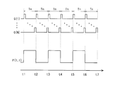
- FIG. 1 is an external perspective view of a portable information terminal according to a first embodiment of the present invention. It is a block diagram which shows the whole structure of the portable information terminal in the said embodiment. It is a block diagram which shows the structure relevant to the display part in the said embodiment. It is a circuit diagram which shows the equivalent circuit of the pixel formation part in the said embodiment. It is a flowchart which shows the flow of a process of the control part which switches normal drive and rest drive in the said embodiment.
- FIG. 6 is a diagram illustrating timings of a scanning signal and a driving video signal during pause driving in the embodiment.
- FIG. 6 is a diagram illustrating timings of a scanning signal and a driving video signal during normal driving in the embodiment.
- FIG. 1 is an external perspective view of a portable information terminal according to the first embodiment of the present invention.
- the portable information terminal 100 includes a display unit 500 made of a liquid crystal panel.
- a transparent touch panel is provided on the upper surface (front surface) of the display unit 500.
- the screen is pressed (contacted) with a finger or a pen (typically a user's dominant hand), the screen is displayed on the screen. The pressed position is detected.
- the configurations of the display unit and the touch panel will be described later.
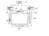
- FIG. 2 is a block diagram showing main configurations of a display unit and an input unit of the portable information terminal according to the present embodiment.
- the portable information terminal 100 includes a control unit 110 that performs various controls including switching control between a pause drive (intermittent drive) and a normal drive (continuous drive), which will be described later, a display unit 500, and a source that drives the display unit 500 A driver 300 and a gate driver 400, a display control circuit 200, a matrix-type resistive touch panel 150 provided on the display unit 500, and a position where a user's finger or pen is pressed on the touch panel 150 are detected.
- X coordinate sensor 130 and Y coordinate sensor 140 and a coordinate processing circuit 120 are provided.
- the touch panel 150 is not a general resistive film type touch panel that detects the contact point of two opposing resistive films in an analog manner, but a large number of transparent electrodes arranged in parallel along the row direction, A large number of transparent electrodes are arranged in parallel along the column direction so as to face each other at a predetermined short distance in the vertical direction.
- the X coordinate sensor 130 is connected to the electrodes along the column direction
- the Y coordinate sensor 140 is connected to the electrodes along the row direction. Therefore, the X coordinate sensor 130 and the Y coordinate sensor 140 can detect when the electrodes in the row direction and the column direction intersect at the position pressed by the user's finger, pen, or the like. Therefore, a large number of coordinates on the touch panel 150 can be individually recognized with a resolution corresponding to the arrangement pitch of the electrodes.
- the touch panel can individually recognize a large number of coordinates
- various known touch panels such as a matrix-type capacitance method, an optical sensor method, and a mechanical sensor method can be employed.
- a plurality of touch panels that can recognize only one coordinate may be used in combination.
- the electrostatic capacity method and the optical sensor method do not need to press the finger against the touch panel unlike the resistive film method, and may be suitable in the present embodiment because it only needs to be lightly touched or brought close to each other. Many.
- a configuration using the fact that it is possible to detect the proximity to a predetermined distance will be described in detail in the third embodiment.
- the method of detecting proximity it is not necessary to detect contact, but even when such a method is adopted, it is referred to as a touch panel here.
- the display unit 500 is composed of an active matrix type liquid crystal panel, and the source driver 300 and the gate driver 400 select each pixel in the liquid crystal panel and assign data to form a display image.
- the source driver 300 and the gate driver 400 select each pixel in the liquid crystal panel and assign data to form a display image.
- FIGS. 3 and 4. FIG.
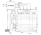
- FIG. 3 is a block diagram showing the overall configuration of the active matrix type liquid crystal display device according to the present embodiment.
- This liquid crystal display device includes a display control circuit 200, a source driver (video signal line drive circuit) 300, a drive control unit including a gate driver (scanning signal line drive circuit) 400, a display unit 500, and a common electrode drive circuit 600.
- the display unit 500 includes a plurality (M) of video signal lines SL (1) to SL (M), a plurality (N) of scanning signal lines GL (1) to GL (N), and a plurality of these.
- a plurality of (M ⁇ N) pixel forming portions provided along the video signal lines SL (1) to SL (M) and the plurality of scanning signal lines GL (1) to GL (N). It is out.
- the display unit 500 As a driving method of the display unit 500, a line inversion method is adopted, but a dot inversion driving method in which the polarity of the video signal voltage to be applied to the liquid crystal portion of the pixel forming unit is inverted for each video signal line is adopted. May be.
- the display unit 500 is, for example, a TN (Twisted Nematic) orientation method and is configured to be normally white.
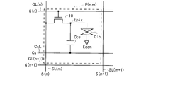
- FIG. 3 shows an equivalent circuit of the pixel formation portion P (n, m) in the display portion 500 of the present embodiment.
- FIG. 4 shows a detailed configuration of a part of the display unit 500 in the embodiment for explaining the connection relation.
- each pixel forming portion P (n, m) has a gate terminal connected to the scanning signal line GL (n) or the scanning signal line GL (n + 1) adjacent thereto, and
- the TFT 10 which is a switching element whose source terminal is connected to the video signal line SL (m) passing through the intersection, the pixel electrode Epix connected to the drain terminal of the TFT 10, and the plurality of pixel forming portions P (i, j)
- the TFT 10 is often made of amorphous silicon, which can be easily and inexpensively manufactured as a semiconductor layer, when high-speed response and small current leakage are not so required.
- IGZO in-Ga-Zn-O
- CGC Continuous grain
- each pixel formation part P (n, m) displays any color of red (R), green (G), and blue (B),
- the pixel formation part P which displays the same color (N, m) are arranged along the video signal lines SL (1) to SL (M), and are repeatedly arranged in the order of RGB along the scanning signal lines GL (1) to GL (N). ing.
- a liquid crystal capacitance (also referred to as “pixel capacitance”) Clc is formed by the pixel electrode Epix and the common electrode Ecom facing each other with the liquid crystal layer interposed therebetween.
- Two video signal lines SL (m) and SL (m + 1) are disposed in the vicinity of the pixel electrode Epix.
- the video signal line SL (m) is connected to the pixel electrode Epix via the TFT 10. It is connected.
- the auxiliary capacitance line CsL is formed in parallel with each scanning signal line GL (n).
- each pixel formation portion P (n, m) the pixel electrode Epix and the auxiliary capacitance line CsL A storage capacitor Ccs is formed between the two. Note that the total capacitance formed between the pixel electrode Epix and the other electrode in one pixel formation portion P (n, m) (that is, the total capacitance connected to the pixel electrode Epix) is also referred to as a pixel capacitance.
- the display control circuit 200 receives a display data signal DAT and a timing control signal TS sent from the outside, and controls a digital image signal DV, a source start pulse signal SSP for controlling the timing of displaying an image on the display unit 500, and a source A clock signal SCK, a latch strobe signal LS, a gate start pulse signal GSP, a gate clock signal GCK, and a polarity inversion signal ⁇ for controlling to invert the potential of the common electrode Ecom are output.
- the gate driver 400 Based on the gate start pulse signal GSP and the gate clock signal GCK output from the display control circuit 200, the gate driver 400 scans the scanning signal lines GL (1) to GL (N) with an active scanning signal G (1). ... G (N) are sequentially applied.
- the gate driver 400 applies a predetermined potential to the scanning signal lines GL (1) to GL (N) simultaneously during a pause period (scanning stop period) to be described later. If this potential is not an active scanning signal G (1) to G (N), that is, if it is a potential that can make the scanning signal line non-selected, each scanning signal in the non-selected state during the scanning period. It may be the same as the inactive scanning signal potential applied to the lines GL (1) to GL (N), or may be a known well-known fixed potential such as a common electrode potential.
- the source driver 300 similarly applies a predetermined potential (different from or the same as the above-mentioned potential) simultaneously to the video signal lines SL (1) to SL (M) during a pause period to be described later. The operation during these pauses will be described later.
- the source driver 300 receives the digital image signal DV, the source start pulse signal SSP, the source clock signal SCK, and the latch strobe signal LS output from the display control circuit 200, and each pixel forming unit P (n, In order to charge the pixel capacity (liquid crystal capacity Clc and auxiliary capacity Ccs) of m), the driving video signals S (1) to S (M) are applied to the video signal lines SL (1) to SL (M). At this time, the source driver 300 sequentially holds the digital image signal DV indicating the voltage to be applied to each of the video signal lines SL (1) to SL (M) at the timing when the pulse of the source clock signal SCK is generated. .
- the held digital image signal DV is converted to an analog voltage at the timing when the pulse of the latch strobe signal LS is generated.
- Such D / A conversion is performed by a gradation voltage generation circuit.
- the gradation voltage generation circuit generates an analog voltage corresponding to each display gradation by, for example, dividing a reference voltage for gradation voltage generation given from the outside of the source driver 300.
- the analog voltage generated by the gradation voltage generation circuit is applied to all the video signal lines SL (1) to SL (M) as a drive video signal all at once. That is, in the present embodiment, the line sequential driving method is adopted as the driving method of the video signal lines SL (1) to SL (M).
- the polarities of the drive video signals S (1) to S (M) applied to the video signal lines SL (1) to SL (M) are inverted for each row as described above.
- the driving video signals S (1) to S (M) when the active scanning signal G (1) is applied to the scanning signal line GL (1) and the active scanning signal G (2) are scanned.
- the drive video signals S (1) to S (M) when applied to the signal line GL (2) have a reverse polarity.
- the common electrode potential Vcom applied to the common electrode Ecom is selected from the predetermined two potentials by the common electrode driving circuit 600 so as to have a phase opposite to the polarity inversion.
- the polarity inversion signal ⁇ indicating the timing of polarity inversion is generated by the display control circuit 200 and supplied to the common electrode driving circuit 600 and the source driver 300. With such a configuration, line inversion driving is realized.
- the driving video signal is applied to the video signal lines SL (1) to SL (M), and the scanning signal is applied to the scanning signal lines GL (1) to GL (N).
- the image is displayed on the display unit 500.
- the auxiliary capacitance line CsL is supplied with a predetermined voltage by a power supply circuit (not shown) and held at the same potential, but may be similarly driven by a circuit similar to the common electrode driving circuit.
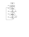
- FIG. 5 is a flowchart showing the flow of processing of the control unit that switches between normal driving and rest driving.
- the control unit 110 performs an initial setting process for performing a control operation on the display control circuit 200 and performing a coordinate receiving operation from the coordinate processing circuit 120.
- the control unit 110 controls the display control circuit 200 to perform pause driving as shown in FIG.
- FIG. 6 is a diagram showing the timing of the scanning signal and the driving video signal during the pause driving.
- the gate driver 400 during the pause driving does not sequentially output the active scanning signals G (1) to G (N) over one frame period, but in one frame period.
- (active) scanning signals G (1) to G (N) are sequentially output.
- the source driver 300 outputs the driving video signals S (1) to S (M) in which the polarity is inverted for each row (by the line sequential driving method) as described above. It is.
- the change in the pixel potential held in the pixel electrode Epix of the pixel formation portion P (1, 1) is illustrated.
- the length of the active period of each of the scanning signals G (1) to G (N) is approximately Ts / N, but is shown with a different length in the figure for easy viewing.
- the scanning signals G (1) to G (N) and the driving video signals S (1) to S (M) are generated during the suspension period Th that is the scanning suspension period from time t12 to time t13. ) Are not output, and the scanning signal lines GL (1) to GL (N) and the video signal lines SL (1) to SL (M) are held (fixed) at a predetermined potential. Therefore, the pixel potential of the pixel formation portion P (1,1) does not change. In practice, the pixel potential gradually decreases during the rest period due to the current leak of the TFT 10 described above, but here, the current leak is very small and is ignored.
- the same operation is performed during the next frame period from time t13 to time t15, and the operation is repeated thereafter.
- the driving by the source driver 300 and the gate driver 400 is intermittently performed.
- the scanning period Ts is, for example, 1/60 [second]
- the pause period Th is, for example, 1/30 [second]. Therefore, in this case, one frame period at the time of rest driving is 1/20 [second].
- these values are merely examples, and other known values may be used.
- the idle period Th is usually longer than the scanning period (typically several times that). In other words, it is generally preferable that one frame period at the time of rest driving is longer than 1/60 [second].
- step S30 the control unit 110 determines whether or not the coordinate indicating the contact position of the finger or the like has been received from the coordinate processing circuit 120. If coordinates due to contact have not been received (No in step S30), the process is repeated until coordinates are received, and if coordinates are received (Yes in step S30), the process proceeds to step S40.
- the X-coordinate sensor 130 and the Y-coordinate sensor 140 that detect the position (contact position) at which the user's finger or pen is pressed on the touch panel 150 are detected at the same period during normal driving and during rest driving. Or may be set so that the detection cycle becomes longer during pause driving. However, even in this case, it is not preferable to set a long detection period in which detection is not performed for the same length as that of the pause period, because the user feels that the operation response is slow.
- step S40 the control unit 110 controls the display control circuit 200 to perform normal driving as shown in FIG. That is, the driving state of the liquid crystal panel shifts from the pause driving state to the normal driving state. This transition is performed immediately after the coordinates are detected, and is not performed after the end of the pause period for pause driving.
- FIG. 7 is a diagram showing the timing of the scanning signal and driving video signal during normal driving.
- the gate driver 400 during normal driving sequentially outputs active scanning signals G (1) to G (N) over one frame period that coincides with the normal period Tn.
- the source driver 300 outputs the driving video signals S (1) to S (M) whose polarity is inverted for each row (in the line sequential driving method) during the normal period Tn. .
- FIG. 7 also illustrates a change in pixel potential held in the pixel electrode Epix of the pixel formation portion P (1, 1).
- the length of the active period of each of the scanning signals G (1) to G (N) is approximately Tn / N, but is shown with a different length in the figure for easy viewing.
- one frame period at the time of normal driving is, for example, 1/60 [second], and is generally driven at a high speed to such an extent that flicker does not occur at the time of moving image display.
- the source driver 300 and the gate driver 400 are continuously driven.
- step S50 the control unit 110 determines whether or not the coordinate is received from the coordinate processing circuit 120. If coordinates are received (Yes in step S50), the process is repeated until no coordinates are received, and if no coordinates are received (No in step S50), the process returns to step S20 and is driven to pause. The above process is repeated until the apparatus stops (S50 ⁇ S20 ⁇ ... ⁇ S50). It should be noted that the polarity inversion signal ⁇ is preferably inverted when transitioning from the rest drive to the normal drive or vice versa.
- the normal drive operation in step S40 is continuously performed for at least several frames.
- pause driving is performed until a finger or the like is brought into contact with the touch panel 150, normal driving is performed during the period of contact, and pause driving is performed when released again. Will work.
- the transition from the normal drive to the rest drive should be performed immediately when the coordinates are not detected.
- the transition from the normal drive to the rest drive should be performed immediately when the coordinates are not detected.
- step S50 normal driving is performed for a period of several seconds (or more) from the time corresponding to several frames, instead of immediately shifting to pause driving.
- pause driving There may be a case where it is preferable to shift to the rest drive after a while. In this case, the power consumption of the apparatus increases because the pause driving time is shortened.
- the pause is performed. Display can be performed immediately (with good response) without waiting for the end of the period.
- the (content) data to be displayed is a still image or a moving image in switching between the pause drive and the normal drive in the control unit 110. And different operations are performed.
- a control operation for the display control circuit 200 by the control unit 110 having such a characteristic will be described with reference to FIG.
- the video here is described as video as video content. However, not only such video but also all or part of a still image changes continuously or intermittently (for example, animation icons may be widely included.
- FIG. 8 is a flowchart showing a flow of processing of the control unit that switches between normal driving and rest driving.
- the processing in steps S10 to S50 shown in FIG. 8 is the same as the processing in steps S10 to S50 shown in FIG. Therefore, the description thereof is omitted, and the processing in subsequent steps S60 and S70 will be described.
- the process immediately proceeds to the next step S60, and normal driving is performed for a predetermined delay time. It is assumed that the processing in the case of being performed is performed when it is determined in step S60 that it is not a moving image. Instead of this configuration, the same configuration as that of the first embodiment may be used.
- step S60 shown in FIG. 8 the control unit 110 determines whether the data being displayed or data to be displayed immediately thereafter (hereinafter referred to as display data) is moving image data. If it is not moving image data (No in step S60), the process returns to step S20 and pause driving is performed, and the above process is repeated until it is determined that the apparatus is stopped or it is a moving image in step S60. (S60 ⁇ S20 ⁇ ... ⁇ S60). Note that, as described above, by setting a predetermined delay time when returning to the pause drive, normal driving is performed only on the liquid crystal panel even when the finger is removed from the touch panel, so that the screen is written until the next scanning period.
- step S60 If it is determined in step S60 that the display data is moving image data, the process proceeds to step S70.
- control unit 110 determines that the display data is moving image data in step S60, and any method may be applied.
- the control unit 110 includes a storage unit that stores image data and a data comparison circuit that compares the stored image data with the current image data while one frame period or a predetermined time elapses.
- a method may be considered in which when the data compared by the comparison circuit matches or substantially matches, it is determined as a still image, and when the data does not match, it is determined as a moving image.
- the function of determining whether or not it is such a moving image may be realized by a circuit or a component different from the control unit 110.
- step S ⁇ b> 70 the control unit 110 determines whether or not coordinates have been received from the coordinate processing circuit 120. If no coordinates are received (No in step S70), the process is repeated until coordinates are received. If coordinates are received (Yes in step S70), the process returns to step S50 and no coordinates are received. The process is repeated until.
- step S60 when the display data is not a moving image (No in step S60), the process does not proceed to step S70, and as a result, the process is exactly the same as the process in the first embodiment.
- the display data is a moving image
- a normal drive is performed until a finger or the like is further brought into contact with the touch panel 150 and released, and the determination in step S60 is performed when the display data is released. Is performed again. Therefore, since the above determination is not performed unless contact is detected, the determination is not repeated unnecessarily, and the power consumption can be further reduced.
- a display device including a touch sensor when a display device including a touch sensor is driven in a driving mode (pause driving) in which a scanning stop period (pause period) is inserted, there is an input to the touch sensor.
- a driving mode normal driving
- switching to a pause driving when there is no input suppresses the power consumption of the apparatus, improves the response of the screen display to the input operation, and displays a moving image
- smooth moving image display can be performed without performing pause driving.
- the configuration of the liquid crystal display device in this embodiment is substantially the same as the configuration of the active matrix liquid crystal display device in the first embodiment shown in FIG. 1, but instead of the matrix type resistive touch panel 150, a matrix type is used.
- the touch panel that employs the electrostatic capacity method or the optical sensor method and can detect the proximity of an object such as a finger or a pen to a predetermined distance is used.
- a touch panel employing a matrix-type capacitance method when the change in capacitance exceeds a predetermined threshold, it can be determined that proximity to a predetermined distance has been detected.
- the touch panel employing the matrix type optical sensor method when the change in the amount of received light exceeds a predetermined threshold, it can be determined that the proximity to the predetermined distance is detected.
- a liquid crystal panel with a built-in sensor function using an optical sensor system is used, and its simple cross-sectional structure and operation principle will be described with reference to FIGS. Note that any touch panel capable of detecting proximity to a predetermined distance, such as a capacitance method, can be applied in the same manner.
- the liquid crystal panel with a built-in optical sensor is either a method for detecting a shadow image or a method for detecting a reflected image (or both a shadow image and a reflected image) when detecting a touch position in the display screen. Is used.
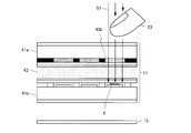
- FIG. 9 is a diagram showing the principle of a method for detecting a shadow image
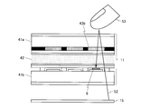
- FIG. 10 is a diagram showing the principle of a method for detecting a reflected image.
- the optical sensor including the photodiode 6 detects the external light 51 transmitted through the glass substrate 41a, the liquid crystal layer 42, and the like. At this time, if the object 53 such as a finger is near the surface of the liquid crystal panel 11, the external light 51 to be incident on the optical sensor is blocked by the object 53. Therefore, it is possible to detect a shadow image of the object 53 by the external light 51 using the optical sensor.
- this image becomes brighter due to the influence of light diffraction and the like as the distance from the object 53 such as a finger increases, so the distance from the object 53 is determined by the amount of current flowing through the photodiode 6 according to the amount of received light. Can be detected.
- the optical sensor including the photodiode 6 detects the reflected light of the backlight 52. More specifically, the backlight light 52 emitted from the backlight 15 passes through the liquid crystal panel 11 and exits from the surface of the liquid crystal panel 11 to the outside. At this time, if the object 53 is near the surface of the liquid crystal panel 11, the backlight 52 is reflected by the object 53. For example, the belly of a human finger reflects light well. The reflected light of the backlight light 52 passes through the glass substrate 41a, the liquid crystal layer 42, etc. and enters the optical sensor. Therefore, the reflection image of the object 53 by the backlight 52 can be detected using the optical sensor. Further, this reflected image becomes darker as the distance from the object 53 such as a finger increases, so that the distance from the object 53 can be detected by the amount of current flowing through the photodiode 6 according to the amount of received light.
- a threshold value of a current value flowing through the photodiode 6 corresponding to a predetermined input detection distance is determined for detection of the touch position.
- a proximity detection distance larger than this input detection distance is determined.
- This proximity detection distance is a distance at which the touch position will be detected almost certainly thereafter. Specifically, when the user performs an operation input, the proximity detection distance is a position where the finger passes in the process of approaching the finger. The corresponding distance. Similarly to the input detection distance, the proximity detection distance also determines a threshold value of the current value flowing through the photodiode 6 corresponding to the distance.
- control unit 110 controls the source driver 300 and the gate driver 400 to be continuously driven in a normal drive mode.
- control unit 110 intermittently drives the source driver 300 and the gate driver 400 in the drive mode of pause driving. Control.
- the control unit 110 does not determine whether or not coordinates indicating a contact position such as a finger have been received from the coordinate processing circuit 120.
- the control unit 110 determines whether a signal for detecting the proximity of an object or information indicating the proximity is received from the optical sensor within the proximity detection distance.
- the normal drive can be started using the time until the finger is actually brought close to the touch position. . Therefore, the normal drive can be started earlier than the configuration in which the normal drive is started after it is detected that the operation input is actually started (configuration in the first embodiment).
- the start of the rest drive is delayed until the object 53 such as a finger leaves further than the proximity detection distance after the actual operation input is completed. Therefore, even when the finger is removed from the touch panel, normal driving is performed in the liquid crystal panel for the delay time, so that a state in which the screen is not rewritten (does not change) until the next scanning period can be reduced or reduced. As a result, it is possible to avoid or reduce the feeling of poor response to the operation, and to avoid or reduce a state that causes an inconvenience in the operation.
- the proximity detection distance is large, but if it is too large, it may be possible to detect false detection due to noise or to detect the proximity of a finger without an operation.
- an appropriate distance larger than the input detection distance is set so as to prevent erroneous detection.
- the delay time can also be set in this embodiment.
- a display device including a touch sensor when driving in a driving mode (pause driving) in which a scanning stop period (pause period) is inserted, the touch sensor is within the proximity detection distance.
- a driving mode normal driving
- switching to a driving mode normal driving
- switching to pause driving when the proximity is no longer detected, thereby reducing the power consumption of the apparatus and performing an input operation
- the response of the screen display to can be further improved.
- the active matrix type liquid crystal display device has been described above as an example. However, if the display device is an active matrix type voltage control display device provided with a scanning period and a rest period, the liquid crystal display device In addition, the present invention can be applied.
- the touch panel is described as an example. However, it is only necessary to include a sensor capable of detecting proximity, contact, or pressing of a finger or an object. For example, an image acquired by a camera outside the device is analyzed. By doing so, the structure which can detect the proximity
- the present invention is applied to a display device such as an active matrix liquid crystal display device, and is particularly suitable for a display device provided with a sensor circuit that accepts an operation input by proximity, contact, or pressing such as a touch sensor. .
Landscapes
- Engineering & Computer Science (AREA)
- Theoretical Computer Science (AREA)
- General Engineering & Computer Science (AREA)
- Physics & Mathematics (AREA)
- General Physics & Mathematics (AREA)
- Human Computer Interaction (AREA)
- Chemical & Material Sciences (AREA)
- Crystallography & Structural Chemistry (AREA)
- Computer Hardware Design (AREA)
- Control Of Indicators Other Than Cathode Ray Tubes (AREA)
- Liquid Crystal Display Device Control (AREA)
Abstract
本装置の制御部(110)は、初期設定後(S10)、表示制御回路(200)に対して、間欠的な休止駆動を行うよう制御する(S20)。その後タッチパネルへの接触が検知されると(S30)、連続的な通常駆動を行うよう制御する(S40)。その後タッチパネルへの接触が検知されなくなると(S50)、休止駆動が行われる(S20)。このように休止駆動時にタッチパネルへの入力がある場合、通常駆動に切り替え、入力が無くなると休止駆動に切り替えることにより、装置の電力消費を抑制しつつ、入力操作に対する画面表示の反応を良好にする。
Description
本発明は、表示装置およびその制御方法に関し、特にタッチセンサを備えるアクティブマトリクス型の表示装置およびその制御方法に関する。
一般に液晶表示装置では、液晶の劣化を抑えると共に表示品位を維持するために交流化駆動が行われている。そして近年、携帯電話機等のような携帯用情報機器は、その処理性能の向上と利用の高度化などによって高品位の表示能力が要求される。そこで上記携帯用情報機器で使用される液晶モジュールの交流化駆動方式として、1水平走査線毎に印加電圧の正負極性を反転させつつ1フレーム毎にも正負極性を反転させる駆動方式(「1ライン反転駆動方式」と呼ばれる)が採用されることが多い。また、垂直・水平方向に隣り合う画素毎に印加電圧の正負極性を反転させつつ1フレーム毎にも正負極性を反転させる駆動方式(「1ドット反転駆動方式」と呼ばれる)も採用されることがある。
しかし、上記1ライン反転駆動方式を採用すると、液晶パネルに印加すべき映像信号における極性反転の頻度が大きくなり(反転周波数が高くなり)、また、駆動用IC(Integrated Circuit)に必要な耐圧の低減のために共通電極の電位の切換周波数も高くなる。その結果、消費電力が増大する。また、1ドット反転駆動方式を採用すると、共通電極を反転駆動できないため、駆動用ICに必要な耐圧が大きくなる。その結果、装置の製造コストが高くなり、また消費電力も増大する。
そこで、近年では、所定の期間だけ印加電圧を変化させない状態とするための走査停止期間を設けることにより、全体として反転周波数を低くする低周波駆動方式が採用されることがある(例えば日本特開2001-312253号公報を参照)。このような走査停止期間(休止期間)の挿入により、携帯電話機等における低消費電力化の要求に応えることができる。
ただこの走査停止期間は、長く設定されるほど消費電力を低減することができる反面で、液晶パネルの画素形成部に設けられる印加電圧を保持するための容量素子において走査停止期間中に電流のリークが生じ、保持されるべき電圧が低下する。このことにより、当該走査停止期間終了後に与えられる印加電圧に応じて表示される(同一であるべき場合の)画素の輝度変化が顕著になる。その結果、この輝度変化がフリッカとして視認されることがある。
また、(押圧、接触、または近接を検知する)タッチセンサを備える表示装置において、タッチセンサへの入力がある場合には、当該入力結果に応じて表示画面が変化するのが通常であることから、上記走査停止期間が挿入される駆動態様でタッチセンサへの入力が(続けて)行われる場合には、装置の応答(反応速度)が遅くなるという問題点を生じる。
しかし当該タッチセンサを備える表示装置において、上記走査停止期間が挿入される駆動態様で駆動しているときにタッチセンサへの入力がある場合、そのままの態様で駆動を続けながら、上記問題点を解消することは非常に困難である。
そこで本発明では、タッチセンサを備える表示装置において、走査停止期間(休止期間)を挿入する駆動態様で駆動している時に当該タッチセンサへの入力がある場合、装置の応答が遅くならないように駆動する表示装置を提供することを目的とする。
本発明の第1の局面は、指または物の近接または接触若しくは押圧による操作入力を受け付けるセンサ回路を備えた表示装置であって、
2次元状に配置された複数の画素回路を含む表示パネルと、
画像を表示するための表示データに応じた信号を前記複数の画素回路に書き込む動作を連続的または間欠的に行う駆動回路と、
前記センサ回路から前記操作入力を示す情報を受け取り、当該情報に基づき前記操作入力が有ると判定される場合、前記駆動回路に前記動作を連続的に行わせ、前記操作入力が無いと判定される場合、前記駆動回路に前記動作を間欠的に行わせる制御部と
を備えることを特徴とする。
2次元状に配置された複数の画素回路を含む表示パネルと、
画像を表示するための表示データに応じた信号を前記複数の画素回路に書き込む動作を連続的または間欠的に行う駆動回路と、
前記センサ回路から前記操作入力を示す情報を受け取り、当該情報に基づき前記操作入力が有ると判定される場合、前記駆動回路に前記動作を連続的に行わせ、前記操作入力が無いと判定される場合、前記駆動回路に前記動作を間欠的に行わせる制御部と
を備えることを特徴とする。
本発明の第2の局面は、本発明の第1の局面において、
前記制御部は、前記表示データが動画データであるか否かを判定し、前記表示データが動画データであると判定される場合、前記駆動回路に前記動作を連続的に行わせることを特徴とする。
前記制御部は、前記表示データが動画データであるか否かを判定し、前記表示データが動画データであると判定される場合、前記駆動回路に前記動作を連続的に行わせることを特徴とする。
本発明の第3の局面は、本発明の第2の局面において、
前記制御部は、前記情報に基づき、前記操作入力が有ると判定された後に前記操作入力が無いと判定される時点または当該時点から所定時間が経過した時点で、前記表示データが動画データであるか否かを判定することを特徴とする。
前記制御部は、前記情報に基づき、前記操作入力が有ると判定された後に前記操作入力が無いと判定される時点または当該時点から所定時間が経過した時点で、前記表示データが動画データであるか否かを判定することを特徴とする。
本発明の第4の局面は、本発明の第1の局面において、
前記制御部は、前記情報に基づき、前記操作入力が有ると判定された後に前記操作入力が無いと判定される時点から所定時間が経過した時点までの間、前記駆動回路に前記動作を連続的に行わせることを特徴とする。
前記制御部は、前記情報に基づき、前記操作入力が有ると判定された後に前記操作入力が無いと判定される時点から所定時間が経過した時点までの間、前記駆動回路に前記動作を連続的に行わせることを特徴とする。
本発明の第5の局面は、本発明の第1の局面において、
前記センサ回路は、予め定められた第1の距離以内の前記指または前記物の接近を検出し、
前記制御部は、前記センサ回路によって前記接近が検出されている間、前記駆動回路に前記動作を連続的に行わせることを特徴とする。
前記センサ回路は、予め定められた第1の距離以内の前記指または前記物の接近を検出し、
前記制御部は、前記センサ回路によって前記接近が検出されている間、前記駆動回路に前記動作を連続的に行わせることを特徴とする。
本発明の第6の局面は、本発明の第5の局面において、
前記センサ回路は、前記第1の距離よりも短く定められる第2の距離以内の前記指または前記物の近接または接触により前記操作入力を受け付けることを特徴とする。
前記センサ回路は、前記第1の距離よりも短く定められる第2の距離以内の前記指または前記物の近接または接触により前記操作入力を受け付けることを特徴とする。
本発明の第7の局面は、本発明の第1の局面において、
前記複数の画素回路は、前記表示パネルに表示されるべき画像を示す複数の映像信号を前記複数の画素形成部に伝達するための複数の映像信号線と、前記複数の映像信号線と交差する複数の走査信号線との交差点にそれぞれ対応してマトリクス状に配置されており、
接続される走査信号線に印加される信号に応じて導通状態または遮断状態となるスイッチング素子と、
接続される映像信号線に前記スイッチング素子を介して接続された画素電極と、
前記複数の画素回路に共通的に設けられた共通電極と、
前記画素電極と前記共通電極とによって形成される画素容量と、
前記画素容量に保持される電圧に応じた表示階調で画素を表示する液晶素子とをそれぞれ含むことを特徴とする。
前記複数の画素回路は、前記表示パネルに表示されるべき画像を示す複数の映像信号を前記複数の画素形成部に伝達するための複数の映像信号線と、前記複数の映像信号線と交差する複数の走査信号線との交差点にそれぞれ対応してマトリクス状に配置されており、
接続される走査信号線に印加される信号に応じて導通状態または遮断状態となるスイッチング素子と、
接続される映像信号線に前記スイッチング素子を介して接続された画素電極と、
前記複数の画素回路に共通的に設けられた共通電極と、
前記画素電極と前記共通電極とによって形成される画素容量と、
前記画素容量に保持される電圧に応じた表示階調で画素を表示する液晶素子とをそれぞれ含むことを特徴とする。
本発明の第8の局面は、本発明の第7の局面において、
前記スイッチング素子は、酸化物半導体からなる半導体層を備える薄膜トランジスタであることを特徴とする。
前記スイッチング素子は、酸化物半導体からなる半導体層を備える薄膜トランジスタであることを特徴とする。
本発明の第9の局面は、指または物の近接または接触若しくは押圧による操作入力を受け付けるセンサ回路と、2次元状に配置された複数の画素回路を含む表示パネルとを備えた表示装置を制御する方法であって、
画像を表示するための表示データに応じた信号を前記複数の画素回路に書き込む動作を連続的または間欠的に行う駆動ステップと、
前記センサ回路から前記操作入力を示す情報を受け取り、当該情報に基づき前記操作入力が有ると判定される場合、前記駆動ステップにおいて前記動作を連続的に行わせ、前記操作入力が無いと判定される場合、前記駆動ステップにおいて前記動作を間欠的に行わせる駆動制御ステップと
を備えることを特徴とする。
画像を表示するための表示データに応じた信号を前記複数の画素回路に書き込む動作を連続的または間欠的に行う駆動ステップと、
前記センサ回路から前記操作入力を示す情報を受け取り、当該情報に基づき前記操作入力が有ると判定される場合、前記駆動ステップにおいて前記動作を連続的に行わせ、前記操作入力が無いと判定される場合、前記駆動ステップにおいて前記動作を間欠的に行わせる駆動制御ステップと
を備えることを特徴とする。
上記本発明の第1の局面によれば、センサ回路からの情報に基づき操作入力が有ると判定される場合、駆動回路に駆動動作を連続的に行わせ、操作入力が無いと判定される場合、駆動回路に駆動動作を間欠的に行わせることにより、装置の電力消費を抑制しつつ、入力操作に対する画面表示の反応を良好にすることができる。
上記本発明の第2の局面によれば、表示データが動画データであると判定される場合、駆動回路に駆動動作を連続的に行わせるので、動画を表示する場合には間欠的な駆動が行われないようにして滑らかな動画表示を行うことができる。
上記本発明の第3の局面によれば、操作入力が有ると判定された後に操作入力が無いと判定される時点(または当該時点から所定時間が経過した時点)で、表示データが動画データであるか否かを判定するので、操作入力が検知されない限り上記判定が行われない。よって、判定が無駄に繰り返されず、電力消費をさらに低減させることができる。
上記本発明の第4の局面によれば、操作入力が有ると判定された後に操作入力が無いと判定される時点から所定時間が経過した時点までの間、駆動回路に駆動動作を連続的に行わせるので、操作入力が完了した直後に画面表示の切り替えが行われる場合、例えば入力操作から表示までに時間がかかる場合または表示自体に時間がかかる場合(例えばアニメーション表示される場合など)、反応よく直ちに表示を行うことができる。
上記本発明の第5の局面によれば、センサ回路により第1の距離(近接検出距離)以内の指または物の接近を検出し、接近が検出されている間、駆動回路に駆動動作を連続的に行わせるので、表示を反応よく直ちに行うことができる。
上記本発明の第6の局面によれば、センサ回路により第1の距離よりも短く定められる第2の距離以内の指または物の近接または接触により操作入力を受け付けるので、操作入力よりも早く連続的な駆動が行われ、操作入力の完了よりも遅く間欠的な駆動が行われることにより、反応よく直ちに表示を行うことができる。
上記本発明の第7の局面によれば、アクティブマトリクス型の液晶表示装置の構成によって、安価に製造することができる。
上記本発明の第8の局面によれば、薄膜トランジスタの半導体層に酸化物半導体が使用されるので、電流リークを非常に小さくすることができ、したがって消費電力を十分に低減することができる。
上記本発明の第9の局面によれば、上記本発明の第1の局面と同様の効果を、表示方法において奏することができる。
以下、本発明の各実施形態について添付図面を参照しつつ説明する。
<1. 第1の実施形態>
<1.1 携帯情報端末の全体構成および動作>
図1は、本発明の第1の実施形態に係る携帯情報端末の外観斜視図である。この携帯情報端末100は、液晶パネルからなる表示部500を備えている。またこの表示部500の上面(表面)には透明なタッチパネルが設けられており、(典型的には利用者の利き手の)指やペンなどで画面を押下(接触)することにより、その画面上の押下位置が検出される。これら表示部およびタッチパネルの構成等については後述する。
<1.1 携帯情報端末の全体構成および動作>
図1は、本発明の第1の実施形態に係る携帯情報端末の外観斜視図である。この携帯情報端末100は、液晶パネルからなる表示部500を備えている。またこの表示部500の上面(表面)には透明なタッチパネルが設けられており、(典型的には利用者の利き手の)指やペンなどで画面を押下(接触)することにより、その画面上の押下位置が検出される。これら表示部およびタッチパネルの構成等については後述する。
図2は、本実施形態に係る携帯情報端末の表示部および入力部の主な構成を示すブロック図である。この携帯情報端末100は、後述する休止駆動(間欠駆動)と通常駆動(連続駆動)との切り替え制御を含む各種制御を行う制御部110と、表示部500と、この表示部500を駆動するソースドライバ300およびゲートドライバ400と、表示制御回路200と、表示部500上に設けられたマトリクス型抵抗膜方式のタッチパネル150と、このタッチパネル150に利用者の指やペンなどが押下された位置を検出するX座標センサ130およびY座標センサ140と、座標処理回路120とを備える。
ここで、タッチパネル150は、対向する2枚の抵抗膜の接触点をアナログ的に検知する一般的な抵抗膜方式のタッチパネルではなく、行方向に沿って平行に配置される多数の透明電極と、これらと垂直方向に所定の短い距離を空けて対向するように列方向に沿って平行に配置される多数の透明電極とを備えている。X座標センサ130は、列方向に沿った上記各電極に接続されており、Y座標センサ140は、行方向に沿った上記各電極に接続されている。したがって、利用者の指やペンなどに押下された位置で交差する行方向および列方向の電極が接触すると、X座標センサ130およびY座標センサ140により検出することができる。よって、電極の配列ピッチに応じた分解能でタッチパネル150上の多数の座標をそれぞれ個別に認識することができる。
また、多数の座標を個別に認識することができるタッチパネルであれば、マトリクス型の静電容量方式や光センサ方式、機械センサ方式など周知の様々な方式のタッチパネルを採用することができる。さらに、1つの座標しか認識できない方式のタッチパネルを複数組み合わせて使用してもよい。なお、一般的に静電容量方式や光センサ方式は抵抗膜方式のように指をタッチパネルに押しつける必要が無く、軽く接触させたり近接させたりするだけでよいので本実施形態において好適である場合が多い。また、所定距離に近接していることを検知可能であることを利用した構成については、第3の実施形態において詳述する。このように近接を検知する方式においては接触を検知する必要はないが、このような方式を採用する場合であっても、ここではタッチパネルと称する。
表示部500は、アクティブマトリクス型の液晶パネルからなり、ソースドライバ300およびゲートドライバ400により液晶パネル内の各画素の選択およびデータ付与が行われ、表示画像が形成される。以下、このような表示のための構成要素からなる液晶表示装置の詳細な構成について、図3および図4を参照して説明する。
図3は、本実施形態に係るアクティブマトリクス型液晶表示装置の全体構成を示すブロック図である。この液晶表示装置は、表示制御回路200、ソースドライバ(映像信号線駆動回路)300、およびゲートドライバ(走査信号線駆動回路)400からなる駆動制御部と、表示部500と、共通電極駆動回路600とを備えている。表示部500は、複数本(M本)の映像信号線SL(1)~SL(M)と、複数本(N本)の走査信号線GL(1)~GL(N)と、それら複数本の映像信号線SL(1)~SL(M)と複数本の走査信号線GL(1)~GL(N)とに沿って設けられた複数個(M×N個)の画素形成部を含んでいる。
この表示部500の駆動方式としては、ライン反転方式が採用されるが、画素形成部の液晶部分へ印加すべき映像信号の電圧を1映像信号線毎に極性反転するドット反転駆動方式が採用されてもよい。またこの表示部500は、例えばTN(Twisted Nematic)配向方式であってノーマリホワイトとなるように構成される。
以下では、走査信号線GL(n)と映像信号線SL(m)との交差点に関連づけて当該交差点近傍(図では当該交差点の右下近傍)に設けられた画素形成部を参照符号“P(n,m)”で示すものとする。図3は、本実施形態の表示部500における画素形成部P(n,m)の等価回路を示している。
また図4は、上記接続関係を説明するための実施形態における表示部500の一部の詳細な構成を示している。なお、上記N,Mの値は、一般的な40インチ以上の液晶テレビにおいては、例えばN=1920×3(RGB色),M=1080である。
これら図3および図4に示すように、各画素形成部P(n,m)は、走査信号線GL(n)またはその隣の走査信号線GL(n+1)にゲート端子が接続されるとともに当該交差点を通過する映像信号線SL(m)にソース端子が接続されたスイッチング素子であるTFT10と、そのTFT10のドレイン端子に接続された画素電極Epixと、上記複数個の画素形成部P(i,j)(i=1~N、j=1~M)に共通的に設けられた共通電極Ecomと、上記複数個の画素形成部P(i,j)(i=1~N、j=1~M)に共通的に設けられ画素電極Epixと共通電極Ecomとの間に挟持された電気光学素子としての液晶層とによって構成される。
上記TFT10は、高速な応答や電流リークの小ささがそれほど求められない場合には、半導体層として容易かつ安価に製造が可能なアモルファスシリコンが使用されることが多いが、ここでは後述するように休止駆動が行われることがあるため、電流リークが非常に小さい(具体的にはアモルファスシリコンが使用する場合に比べて一桁以上小さい)In-Ga-Zn-O(IGZO)系の酸化物半導体が使用されるものとする。もちろん、電流リークの問題はあるが、上記アモルファスシリコンや、CG (Continuous grain) シリコンなど、その他の周知の半導体を使用することもできる。
なお、各画素形成部P(n,m)は、赤色(R)、緑色(G)、青色(B)のいずれかの色を表示するものであって、同じ色を表示する画素形成部P(n,m)が映像信号線SL(1)~SL(M)に沿って配置されており、かつ走査信号線GL(1)~GL(N)に沿ってRGBの順で繰り返して配置されている。
各画素形成部P(n,m)では、画素電極Epixと、それに液晶層を挟んで対向する共通電極Ecomとによって液晶容量(「画素容量」ともいう)Clcが形成されている。画素電極Epix近傍には、2本の映像信号線SL(m),SL(m+1)が配設されており、これらのうちの映像信号線SL(m)がTFT10を介して当該画素電極Epixに接続されている。また、図4に示すように各走査信号線GL(n)と平行に補助容量線CsLが形成されており、各画素形成部P(n,m)では、画素電極Epixと補助容量線CsLとの間に補助容量Ccsが形成されている。なお、1つの画素形成部P(n,m)において画素電極Epixと他の電極との間に形成される全容量(すなわち画素電極Epixに繋がる全容量)を画素容量ともいう。
表示制御回路200は、外部から送られる表示データ信号DATとタイミング制御信号TSとを受け取り、デジタル画像信号DVと、表示部500に画像を表示するタイミングを制御するためのソーススタートパルス信号SSP、ソースクロック信号SCK、ラッチストローブ信号LS、ゲートスタートパルス信号GSP、およびゲートクロック信号GCKと、共通電極Ecomの電位を反転させるよう制御するための極性反転信号φとを出力する。
ゲートドライバ400は、表示制御回路200から出力されたゲートスタートパルス信号GSPとゲートクロック信号GCKとに基づいて、各走査信号線GL(1)~GL(N)にアクティブな走査信号G(1)~G(N)を順次印加する。
また、ゲートドライバ400は、後述する休止期間(走査停止期間)中、各走査信号線GL(1)~GL(N)に対して同時に所定の電位を印加する。この電位は、アクティブな走査信号G(1)~G(N)でなければ、すなわち走査信号線を非選択状態とすることができる電位であれば、走査期間中において非選択状態の各走査信号線GL(1)~GL(N)に対して与えられる非アクティブな走査信号電位と同じであってもよいし、共通電極電位など予め定められた周知の固定電位であってもよい。さらに、ソースドライバ300も同様に、後述する休止期間中、各映像信号線SL(1)~SL(M)に対して同時に(上記電位とは異なるまたは同一の)所定の電位を印加する。これらの休止期間中の動作については後述する。
ソースドライバ300は、表示制御回路200から出力されたデジタル画像信号DV、ソーススタートパルス信号SSP、ソースクロック信号SCK、およびラッチストローブ信号LSを受け取り、表示部500内の各画素形成部P(n,m)の画素容量(液晶容量Clcおよび補助容量Ccs)を充電するために駆動用映像信号S(1)~S(M)を各映像信号線SL(1)~SL(M)に印加する。このとき、ソースドライバ300では、ソースクロック信号SCKのパルスが発生するタイミングで、各映像信号線SL(1)~SL(M)に印加すべき電圧を示すデジタル画像信号DVが順次に保持される。そして、ラッチストローブ信号LSのパルスが発生するタイミングで、上記保持されたデジタル画像信号DVがアナログ電圧に変換される。このようなD/A変換は、階調電圧生成回路により行われる。この階調電圧生成回路は、例えばソースドライバ300の外部から与えられる階調電圧生成のための基準電圧を分圧することにより、各表示階調に対応するアナログ電圧を生成する。この階調電圧生成回路により生成されたアナログ電圧は、駆動用映像信号として全ての映像信号線SL(1)~SL(M)に一斉に印加される。すなわち、本実施形態においては、映像信号線SL(1)~SL(M)の駆動方式には線順次駆動方式が採用されている。
ここで、各映像信号線SL(1)~SL(M)に印加される駆動用映像信号S(1)~S(M)の極性は、前述したように行毎に反転される。例えば、アクティブな走査信号G(1)が走査信号線GL(1)に印加されているときの駆動用映像信号S(1)~S(M)と、アクティブな走査信号G(2)が走査信号線GL(2)に印加されているときの駆動用映像信号S(1)~S(M)とは逆極性となる。また消費電力低減のため、上記極性反転と逆位相となるよう、共通電極Ecomに印加される共通電極電位Vcomは、共通電極駆動回路600によって所定の2つの電位から選択されて与えられる。なお、この極性反転のタイミングを示す極性反転信号φは、表示制御回路200により生成され共通電極駆動回路600およびソースドライバ300に与えられる。このような構成によりライン反転駆動が実現される。
以上のようにして、各映像信号線SL(1)~SL(M)に駆動用映像信号が印加され、各走査信号線GL(1)~GL(N)に走査信号が印加されることにより、表示部500に画像が表示される。なお、補助容量線CsLは、図示されない電源回路により所定電圧の供給を受けて同電位に保持されるが、共通電極駆動回路と同様の回路により同様に駆動されてもよい。次に、制御部110による表示制御回路200に対する制御動作について図5を参照して説明する。
<1.2 制御部による制御動作>
図5は、通常駆動と休止駆動とを切り替える制御部の処理の流れを示すフローチャートである。図5に示すステップS10において、制御部110は表示制御回路200に対する制御動作を行うため、および座標処理回路120からの座標受け取り動作を行うための初期設定処理を行う。続いて、ステップS20において、制御部110は表示制御回路200に対して、図6に示すような休止駆動を行うよう制御する。
図5は、通常駆動と休止駆動とを切り替える制御部の処理の流れを示すフローチャートである。図5に示すステップS10において、制御部110は表示制御回路200に対する制御動作を行うため、および座標処理回路120からの座標受け取り動作を行うための初期設定処理を行う。続いて、ステップS20において、制御部110は表示制御回路200に対して、図6に示すような休止駆動を行うよう制御する。
図6は、休止駆動時における走査信号および駆動用映像信号のタイミングを示す図である。図6に示されるように、休止駆動中のゲートドライバ400は、1フレーム期間に渡ってアクティブな走査信号G(1)~G(N)を順次出力するのではなく、1フレーム期間のうちの時刻t11から時刻t12までの走査期間Ts中に、(アクティブな)走査信号G(1)~G(N)を順次出力する。なお、この走査期間Ts中に、ソースドライバ300は、行毎に極性反転させた駆動用映像信号S(1)~S(M)を(線順次駆動方式で)出力する点については前述したとおりである。図では画素形成部P(1,1)の画素電極Epixに保持される画素電位の変化が例示されている。また、上記走査信号G(1)~G(N)それぞれのアクティブ期間の長さは、ほぼTs/Nであるが、図では見やすくするため異なる長さで記載されている。
この走査期間Tsが終了すると、時刻t12から時刻t13までの走査停止期間中である休止期間Th中、走査信号G(1)~G(N)および駆動用映像信号S(1)~S(M)は出力されず、各走査信号線GL(1)~GL(N)および各映像信号線SL(1)~SL(M)は、所定の電位に保持される(固定される)。したがって、画素形成部P(1,1)の画素電位も変化しない。なお、実際には、前述したTFT10の電流リークにより上記画素電位は休止期間中に少しずつ低下するが、ここでは上記電流リークが非常に小さいため無視するものとする。こうして1フレーム期間中の動作が終了すると、続く時刻t13から時刻t15までの次のフレーム期間中も同様の動作が行われ、その後も当該動作が繰り返される。こうして、休止駆動中において、上記ソースドライバ300およびゲートドライバ400による駆動は間欠的になされることになる。
なお、走査期間Tsは、例えば1/60[秒]であり、休止期間Thは、例えば1/30[秒]である。よってこの場合には休止駆動時における1フレーム期間は1/20[秒]となる。もちろんこれらの値は一例であって、その他の周知の値であってもよいが、休止期間Thは低消費電力化のために設けられるので、通常は走査期間以上(典型的にはその数倍ないし数十倍程度またはそれ以上)の長さが好適であり、そのことから休止駆動時における1フレーム期間は1/60[秒]よりも長いことが一般的には好適となる。
以上のような休止駆動中に、本実施形態ではステップS30において、制御部110は、座標処理回路120から指などの接触位置を示す座標を受け取ったか否かを判定する。接触による座標を受け取っていない場合(ステップS30においてNoである場合)、処理は座標を受け取るまで繰り返され、座標を受け取る場合(ステップS30においてYesである場合)、処理はステップS40へ進む。なお、このタッチパネル150において利用者の指やペンなどが押下された位置(接触位置)を検出するX座標センサ130およびY座標センサ140は、通常駆動中と休止駆動中とで同様の周期で検出を行ってもよいし、休止駆動中には検出周期が長くなるように設定されていてもよい。ただしこの場合であっても、休止期間と同様の長さだけ検出が行われないような長い検出周期を設定すると、利用者にとって操作の反応が鈍く感じられるため好ましくない。
次にステップS40において、制御部110は表示制御回路200に対して、図7に示すような通常駆動を行うよう制御する。すなわち、液晶パネルの駆動状態は、休止駆動状態から通常状駆動状態へ移行する。なお、この移行は、上記座標が検出されると直ちに行われるものであって、休止駆動のための休止期間の終了を待って行われるわけではない。
図7は、通常駆動時における走査信号および駆動用映像信号のタイミングを示す図である。図7に示されるように、通常駆動中のゲートドライバ400は、通常期間Tnと一致する1フレーム期間に渡ってアクティブな走査信号G(1)~G(N)を順次出力する。なお、この通常期間Tn中に、ソースドライバ300は、行毎に極性反転させた駆動用映像信号S(1)~S(M)を(線順次駆動方式で)出力する点については同様である。また、図6の場合と同様、図7においても画素形成部P(1,1)の画素電極Epixに保持される画素電位の変化が例示されている。また、上記走査信号G(1)~G(N)それぞれのアクティブ期間の長さは、ほぼTn/Nであるが、図では見やすくするため異なる長さで記載されている。ここで、通常駆動時における1フレーム期間は、例えば1/60[秒]であり、動画表示時においてもフリッカが生じない程度に高速に駆動されるのが一般的である。以上のように、通常駆動中において、上記ソースドライバ300およびゲートドライバ400による駆動は連続的になされることになる。
以上のような通常駆動中に、本実施形態ではステップS50において、制御部110は、座標処理回路120から座標を受け取ったか否かを判定する。座標を受け取っている場合(ステップS50においてYesである場合)、処理は座標を受け取らなくなるまで繰り返され、座標を受け取らない場合(ステップS50においてNoである場合)、処理はステップS20へ戻って休止駆動が行われ、装置が停止するまで上記処理が繰り返される(S50→S20→…→S50)。なお、休止駆動から通常駆動へ遷移する場合、またはその逆の場合、極性反転信号φは反転されることが好ましい。
ここで一般的に、タッチパネル150において利用者の指やペンなどが押下される場合、どれだけ素早く動かしたとしても、上記通常期間Tnの少なくとも数倍以上の長さは押下状態が継続されるのが通常である。したがって、上記ステップS40における通常駆動動作は、少なくとも数フレーム以上は継続して行われる。このように、本液晶パネルでは、タッチパネル150に指などを接触させるまでは休止駆動が行われ、接触させている期間中は通常駆動が行われ、再び離すと休止駆動が行われる、という態様で動作することになる。
もっとも、座標が検出されると直ちに行われるべき休止駆動から通常駆動への移行とは異なり、通常駆動から休止駆動への移行は、座標が検出されなくなると直ちに行われるべきである、とは言えない場合も考えられる。例えば、利用者によってタッチパネルを押下する操作が行われる場合、当該操作入力に対応する(例えば入力コマンドに応じた)処理を行い、その後に適した画面を表示する処理を行うと、操作入力の時点から比較的時間が経過していることがある。この時、既に入力操作が完了してタッチパネルから指が離れていると、休止駆動中に画面表示を行うことになり、利用者にとって表示(反応)が遅く感じられることもあり得る。そこで、ステップS50において、(検出された)座標を受け取らない場合、すぐに休止駆動に移行するのではなく、数フレーム分に対応する時間から数秒程度(またはそれ以上)の時間、通常駆動を行った後に休止駆動に移行することが好ましい場合も考えられる。この場合には、休止駆動時間が短くなるため装置の電力消費は増加するが、入力操作から表示までに時間がかかる場合または表示自体に時間がかかる場合(例えばアニメーション表示される場合など)、休止期間の終了を待つことなく、(反応よく)直ちに表示を行うことができる。
このように休止駆動へ戻る時に所定の遅れ時間を設定することにより、タッチパネルから指を離してもなお液晶パネルにおいて上記遅れ時間だけ通常駆動が行われるため、次の走査期間まで画面が書き換わらない(変化しない)という状態が生じない。その結果、操作に対する反応が悪く感じられることがなく、操作に不都合を生じる状態を回避することができる。
<1.3 効果>
以上のように、本実施形態では、タッチセンサを備える表示装置において、走査停止期間(休止期間)を挿入する駆動態様(休止駆動)で駆動している時に当該タッチセンサへの入力がある場合、走査停止期間を挿入しない駆動態様(通常駆動)に切り替え、入力が無くなると休止駆動に切り替えることにより、装置の電力消費を抑制しつつ、入力操作に対する画面表示の反応を良好にすることができる。
以上のように、本実施形態では、タッチセンサを備える表示装置において、走査停止期間(休止期間)を挿入する駆動態様(休止駆動)で駆動している時に当該タッチセンサへの入力がある場合、走査停止期間を挿入しない駆動態様(通常駆動)に切り替え、入力が無くなると休止駆動に切り替えることにより、装置の電力消費を抑制しつつ、入力操作に対する画面表示の反応を良好にすることができる。
<2. 第2の実施形態>
<2.1 液晶表示装置の全体構成および動作>
本実施形態における液晶表示装置の構成は、図1に示す第1の実施形態におけるアクティブマトリクス型液晶表示装置の構成と同様であるので、説明を省略する。
<2.1 液晶表示装置の全体構成および動作>
本実施形態における液晶表示装置の構成は、図1に示す第1の実施形態におけるアクティブマトリクス型液晶表示装置の構成と同様であるので、説明を省略する。
本実施形態では、第1の実施形態の場合とは異なり、制御部110における休止駆動と通常駆動との切り替えにおいて、表示されるべき(コンテンツ)データが静止画である場合と、動画である場合とで、異なる動作が行われる。以下、このように特徴的な制御部110による表示制御回路200に対する制御動作について、図8を参照して説明する。なお、ここでの動画とは、映像コンテンツとしての動画であるものして説明するが、このような動画だけではなく、静止画の全部または一部が連続的または断続的にに変化する場合(例えばアニメーションアイコンなど)を広く含んでもよい。
<2.2 制御部による制御動作>
図8は、通常駆動と休止駆動とを切り替える制御部の処理の流れを示すフローチャートである。この図8に示すステップS10~S50における処理は、図5に示すステップS10~S50における処理と同一である。したがって、その説明を省略し、続くステップS60,S70における処理について説明する。ただし、ここでは第1の実施形態の場合とは異なり、ステップS50において、(検出された)座標を受け取らない場合、直ちに次のステップS60の処理に移行し、通常駆動が所定の遅れ時間だけ行われる場合の処理は、続くステップS60において、動画でないと判定される場合に行われるものとする。なおこの構成に代えて、第1の実施形態の場合と同様の構成としてもよい。
図8は、通常駆動と休止駆動とを切り替える制御部の処理の流れを示すフローチャートである。この図8に示すステップS10~S50における処理は、図5に示すステップS10~S50における処理と同一である。したがって、その説明を省略し、続くステップS60,S70における処理について説明する。ただし、ここでは第1の実施形態の場合とは異なり、ステップS50において、(検出された)座標を受け取らない場合、直ちに次のステップS60の処理に移行し、通常駆動が所定の遅れ時間だけ行われる場合の処理は、続くステップS60において、動画でないと判定される場合に行われるものとする。なおこの構成に代えて、第1の実施形態の場合と同様の構成としてもよい。
図8に示すステップS60において、制御部110は、表示中のデータまたは直後に表示されるべきデータ(以下、表示データという)が動画データであるか否かを判別する。動画データでない場合(ステップS60においてNoである場合)、処理はステップS20へ戻って休止駆動が行われ、装置が停止するか、またはステップS60において動画であると判定されるまで、上記処理が繰り返される(S60→S20→…→S60)。なお前述したように休止駆動へ戻る時に所定の遅れ時間を設定することにより、タッチパネルから指を離してもなお液晶パネルにおいて上記遅れ時間だけ通常駆動が行われるため、次の走査期間まで画面が書き換わらない(変化しない)という状態が生じず、操作に対する反応が悪く感じられ、操作にも不都合を生じる、という状態を回避することができる。またこのステップS60において、表示データが動画データであると判別される場合、処理はステップS70へ進む。
ここで、上記ステップS60において、制御部110がどのように表示データを動画データであると判別するかについては、様々な周知の手法があり、どのような手法を適用してもよい。例えば、制御部110は、1フレーム期間または所定時間が経過する間、画像データを保存する記憶部と、保存された画像データと現時点の画像データとを比較するデータ比較回路とを備え、当該データ比較回路により比較されたデータが一致または略一致する場合には静止画であると判定し、一致しなければ動画であると判定する手法などが考えられる。またこのような動画であるか否かを判別する機能は、制御部110とは異なる回路または構成要素によって実現されてもよい。
続くステップS70において、制御部110は、座標処理回路120から座標を受け取ったか否かを判定する。座標を受け取っていない場合(ステップS70においてNoである場合)、処理は座標を受け取るまで繰り返され、座標を受け取る場合(ステップS70においてYesである場合)、処理はステップS50へ戻り、座標を受け取らなくなるまで処理が繰り返される。
このように、本実施形態では、表示データが動画でない場合(ステップS60においてNoである場合)には、上記ステップS70の処理へ進まないため、結果的に第1の実施形態における処理と全く同様の処理となるが、表示データが動画である場合には、当該判定がなされた後、さらにタッチパネル150に指などを接触させ、かつ離すまでは通常駆動が行われ、離した時にステップS60における判定が再度行われる構成となっている。したがって、接触が検知されない限り上記判定が行われないので、判定が無駄に繰り返されず、電力消費をさらに低減させることができる。
<2.3 効果>
以上のように、本実施形態では、タッチセンサを備える表示装置において、走査停止期間(休止期間)を挿入する駆動態様(休止駆動)で駆動している時に当該タッチセンサへの入力がある場合、走査停止期間を挿入しない駆動態様(通常駆動)に切り替え、入力が無くなると休止駆動に切り替えることにより、装置の電力消費を抑制しつつ、入力操作に対する画面表示の反応を良好にし、動画を表示する場合には休止駆動が行われないようにして滑らかな動画表示を行うことができる。
以上のように、本実施形態では、タッチセンサを備える表示装置において、走査停止期間(休止期間)を挿入する駆動態様(休止駆動)で駆動している時に当該タッチセンサへの入力がある場合、走査停止期間を挿入しない駆動態様(通常駆動)に切り替え、入力が無くなると休止駆動に切り替えることにより、装置の電力消費を抑制しつつ、入力操作に対する画面表示の反応を良好にし、動画を表示する場合には休止駆動が行われないようにして滑らかな動画表示を行うことができる。
<3. 第3の実施形態>
<3.1 液晶表示装置の全体構成および動作>
本実施形態における液晶表示装置の構成は、図1に示す第1の実施形態におけるアクティブマトリクス型液晶表示装置の構成とほぼ同様であるが、マトリクス型抵抗膜方式のタッチパネル150に代えて、マトリクス型の静電容量方式や光センサ方式を採用し、指やペンなどの物の所定距離への近接を検知可能なタッチパネルが使用される。
<3.1 液晶表示装置の全体構成および動作>
本実施形態における液晶表示装置の構成は、図1に示す第1の実施形態におけるアクティブマトリクス型液晶表示装置の構成とほぼ同様であるが、マトリクス型抵抗膜方式のタッチパネル150に代えて、マトリクス型の静電容量方式や光センサ方式を採用し、指やペンなどの物の所定距離への近接を検知可能なタッチパネルが使用される。
例えば、マトリクス型の静電容量方式を採用したタッチパネルでは、静電容量の変化が所定の閾値を超える場合、所定距離への近接を検知したと判定することができる。また、マトリクス型の光センサ方式を採用したタッチパネルでは、受光量の変化が所定の閾値を超える場合、所定距離への近接を検知したと判定することができる。本実施形態では、光センサ方式を使用したセンサ機能内蔵型の液晶パネルが使用されるものとし、その簡単な断面構造および動作原理を図9および図10を参照して説明する。なお、静電容量方式など、所定距離への近接を検知可能なタッチパネルであれば同様に適用可能である。
本実施形態における光センサ内蔵型の液晶パネルは、表示画面内のタッチ位置を検知するときに、影像を検知する方法と反射像(あるいは、影像と反射像の両方)を検知する方法のいずれかを使用する。
図9は、影像を検知する方法の原理を示す図であり、図10は、反射像を検知する方法の原理を示す図である。影像を検知する方法(図9)では、フォトダイオード6を含む光センサは、ガラス基板41aや液晶層42などを透過した外光51を検知する。このときに指などの対象物53が液晶パネル11の表面付近にあると、光センサに入射すべき外光51が対象物53によって遮られる。したがって、光センサを用いて、外光51による対象物53の影像を検知することができる。またこの影像は、指などの対象物53からの距離が離れるほど、光の回折などの影響により明るくなるため、受光量に応じてフォトダイオード6を流れる電流量により、対象物53との距離を検出することができる。
また反射像を検知する方法(図10)では、フォトダイオード6を含む光センサは、バックライト光52の反射光を検知する。より詳細には、バックライト15から出射されたバックライト光52は、液晶パネル11を透過して液晶パネル11の表面から外部に出る。このときに対象物53が液晶パネル11の表面付近にあると、バックライト光52は対象物53で反射する。例えば、人間の指の腹は光をよく反射する。バックライト光52の反射光は、ガラス基板41aや液晶層42などを透過して光センサに入射する。したがって、光センサを用いて、バックライト光52による対象物53の反射像を検知することができる。またこの反射像は、指などの対象物53からの距離が離れるほど、暗くなるため、受光量に応じてフォトダイオード6を流れる電流量により、対象物53との距離を検出することができる。
ここで、以上のように指などの対象物53の影像または反射像の明るさに基づき、対象物53までの距離を計測することは可能であるが、検出ノイズを排除して確実に対象物53の近接を検知するため、タッチ位置の検出には、予め定められた入力検出距離に対応するフォトダイオード6を流れる電流値の閾値が定められている。この入力検出距離以内の距離に指などを近接させると、タッチ位置が検出される。
さらに、本実施形態では、この入力検出距離よりも大きい近接検出距離が定められる。この近接検出距離は、その後ほぼ確実にタッチ位置の検出がなされるであろう距離であって、具体的には利用者が操作入力を行う際に、指を近づけていく過程で通過する位置に対応する距離である。この近接検出距離も、上記入力検出距離と同様に、距離に対応するフォトダイオード6を流れる電流値の閾値が定められる。
光センサがこの近接検出距離以内に指などの対象物53の近接を検知すると、制御部110は、通常駆動の駆動態様で上記ソースドライバ300およびゲートドライバ400を連続的に駆動するよう制御する。また、光センサがこの近接検出距離以内に指などの対象物53の近接を検知しない場合、制御部110は、休止駆動の駆動態様で上記ソースドライバ300およびゲートドライバ400を間欠的に駆動するよう制御する。
すなわち、第1の実施形態のように、図5に示すステップS30,S50において、制御部110は、座標処理回路120から指などの接触位置を示す座標を受け取ったか否かを判定するのではなく、本実施形態において、制御部110は、光センサから近接検出距離以内に対象物の近接を検知する信号または近接を示す情報を受け取った否かを判定する。このように入力検出距離よりも大きい近接検出距離で対象物の近接を検知し通常駆動を行う構成により、実際にタッチ位置まで指を近づけるまでの時間を利用して通常駆動を開始することができる。したがって、実際に操作入力が開始されたことが検知された後に通常駆動を開始する構成(第1の実施形態の構成)よりも、さらに早く通常駆動を開始することができる。
また休止駆動へ戻る時にも、実際の操作入力が終了した後、近接検出距離よりも遠くへ指などの対象物53が離れるまで休止駆動の開始が遅れる。したがって、タッチパネルから指を離してもなお液晶パネルにおいて上記遅れ時間だけ通常駆動が行われるため、次の走査期間まで画面が書き換わらない(変化しない)という状態が生じないか少なくすることができる。その結果、操作に対する反応が悪く感じられることがないか少なくすることができ、操作に不都合を生じる状態を回避または低減することができる。
なお、このように駆動を早く開始するためには近接検出距離は大きい方が好ましいが、あまり大きくするとノイズによる誤検出や、操作を伴わない指などの近接を検出することも考えられるため、このように誤った検出が行われない程度の距離であって、入力検出距離よりも大きい適宜の距離が設定される。また、上記遅れ時間の設定は、本実施形態においても行うことができる。
<3.2 効果>
以上のように、本実施形態では、タッチセンサを備える表示装置において、走査停止期間(休止期間)を挿入する駆動態様(休止駆動)で駆動している時に当該タッチセンサへ上記近接検出距離以内の指などの近接が検出される場合、走査停止期間を挿入しない駆動態様(通常駆動)に切り替え、上記近接が検出されなくなると休止駆動に切り替えることにより、装置の電力消費を抑制しつつ、入力操作に対する画面表示の反応をさらに良好にすることができる。
以上のように、本実施形態では、タッチセンサを備える表示装置において、走査停止期間(休止期間)を挿入する駆動態様(休止駆動)で駆動している時に当該タッチセンサへ上記近接検出距離以内の指などの近接が検出される場合、走査停止期間を挿入しない駆動態様(通常駆動)に切り替え、上記近接が検出されなくなると休止駆動に切り替えることにより、装置の電力消費を抑制しつつ、入力操作に対する画面表示の反応をさらに良好にすることができる。
<4. 変形例>
以上ではアクティブマトリクス型の液晶表示装置を例に挙げて説明したが、アクティブマトリクス型の電圧制御による表示装置であって、走査期間と休止期間とが設けられた表示装置であれば、液晶表示装置以外にも本発明の適用が可能である。
以上ではアクティブマトリクス型の液晶表示装置を例に挙げて説明したが、アクティブマトリクス型の電圧制御による表示装置であって、走査期間と休止期間とが設けられた表示装置であれば、液晶表示装置以外にも本発明の適用が可能である。
また上記表示装置では、タッチパネルを備える例で説明したが、指や物などの近接、接触、または押圧を検知可能なセンサを備えていればよく、例えば装置外部のカメラにより取得された画像を解析することにより、表示装置に対する指や物などの近接などを検知可能な構成であってもよい。
本発明は、アクティブマトリックス型の液晶表示装置などの表示装置に適用されるものであって、特にタッチセンサなどの近接または接触若しくは押圧による操作入力を受け付けるセンサ回路を備えた表示装置に適している。
10 …TFT(スイッチング素子)
110 …制御部
150 …タッチパネル
200 …表示制御回路
300 …ソースドライバ
400 …ゲートドライバ
500 …表示部
600 …共通電極駆動回路
DAT …表示データ信号(画像信号)
DV …デジタル画像信号
φ …極性反転信号
Clc …液晶容量(画素容量)
Ccs …補助容量
Ecom …共通電極
Epix …画素電極
GL(n) …走査信号線(n=1~N)
SL(m) …映像信号線(m=1~M)
P(n,m) …画素形成部(n=1~N、m=1~M)
110 …制御部
150 …タッチパネル
200 …表示制御回路
300 …ソースドライバ
400 …ゲートドライバ
500 …表示部
600 …共通電極駆動回路
DAT …表示データ信号(画像信号)
DV …デジタル画像信号
φ …極性反転信号
Clc …液晶容量(画素容量)
Ccs …補助容量
Ecom …共通電極
Epix …画素電極
GL(n) …走査信号線(n=1~N)
SL(m) …映像信号線(m=1~M)
P(n,m) …画素形成部(n=1~N、m=1~M)
Claims (9)
- 指または物の近接または接触若しくは押圧による操作入力を受け付けるセンサ回路を備えた表示装置であって、
2次元状に配置された複数の画素回路を含む表示パネルと、
画像を表示するための表示データに応じた信号を前記複数の画素回路に書き込む動作を連続的または間欠的に行う駆動回路と、
前記センサ回路から前記操作入力を示す情報を受け取り、当該情報に基づき前記操作入力が有ると判定される場合、前記駆動回路に前記動作を連続的に行わせ、前記操作入力が無いと判定される場合、前記駆動回路に前記動作を間欠的に行わせる制御部と
を備えることを特徴とする、表示装置。 - 前記制御部は、前記表示データが動画データであるか否かを判定し、前記表示データが動画データであると判定される場合、前記駆動回路に前記動作を連続的に行わせることを特徴とする、請求項1に記載の表示装置。
- 前記制御部は、前記情報に基づき、前記操作入力が有ると判定された後に前記操作入力が無いと判定される時点または当該時点から所定時間が経過した時点で、前記表示データが動画データであるか否かを判定することを特徴とする、請求項2に記載の表示装置。
- 前記制御部は、前記情報に基づき、前記操作入力が有ると判定された後に前記操作入力が無いと判定される時点から所定時間が経過した時点までの間、前記駆動回路に前記動作を連続的に行わせることを特徴とする、請求項1に記載の表示装置。
- 前記センサ回路は、予め定められた第1の距離以内の前記指または前記物の接近を検出し、
前記制御部は、前記センサ回路によって前記接近が検出されている間、前記駆動回路に前記動作を連続的に行わせることを特徴とする、請求項1に記載の表示装置。 - 前記センサ回路は、前記第1の距離よりも短く定められる第2の距離以内の前記指または前記物の近接または接触により前記操作入力を受け付けることを特徴とする、請求項5に記載の表示装置。
- 前記複数の画素回路は、前記表示パネルに表示されるべき画像を示す複数の映像信号を前記複数の画素形成部に伝達するための複数の映像信号線と、前記複数の映像信号線と交差する複数の走査信号線との交差点にそれぞれ対応してマトリクス状に配置されており、
接続される走査信号線に印加される信号に応じて導通状態または遮断状態となるスイッチング素子と、
接続される映像信号線に前記スイッチング素子を介して接続された画素電極と、
前記複数の画素回路に共通的に設けられた共通電極と、
前記画素電極と前記共通電極とによって形成される画素容量と、
前記画素容量に保持される電圧に応じた表示階調で画素を表示する液晶素子とをそれぞれ含むことを特徴とする、請求項1に記載の表示装置。 - 前記スイッチング素子は、酸化物半導体からなる半導体層を備える薄膜トランジスタであることを特徴とする、請求項7に記載の表示装置。
- 指または物の近接または接触若しくは押圧による操作入力を受け付けるセンサ回路と、2次元状に配置された複数の画素回路を含む表示パネルとを備えた表示装置を制御する方法であって、
画像を表示するための表示データに応じた信号を前記複数の画素回路に書き込む動作を連続的または間欠的に行う駆動ステップと、
前記センサ回路から前記操作入力を示す情報を受け取り、当該情報に基づき前記操作入力が有ると判定される場合、前記駆動ステップにおいて前記動作を連続的に行わせ、前記操作入力が無いと判定される場合、前記駆動ステップにおいて前記動作を間欠的に行わせる駆動制御ステップと
を備えることを特徴とする、制御方法。
Applications Claiming Priority (2)
| Application Number | Priority Date | Filing Date | Title |
|---|---|---|---|
| JP2011171606 | 2011-08-05 | ||
| JP2011-171606 | 2011-08-05 |
Publications (1)
| Publication Number | Publication Date |
|---|---|
| WO2013021846A1 true WO2013021846A1 (ja) | 2013-02-14 |
Family
ID=47668358
Family Applications (1)
| Application Number | Title | Priority Date | Filing Date |
|---|---|---|---|
| PCT/JP2012/069314 Ceased WO2013021846A1 (ja) | 2011-08-05 | 2012-07-30 | 表示装置およびその制御方法 |
Country Status (2)
| Country | Link |
|---|---|
| TW (1) | TW201308158A (ja) |
| WO (1) | WO2013021846A1 (ja) |
Cited By (7)
| Publication number | Priority date | Publication date | Assignee | Title |
|---|---|---|---|---|
| JP2014222272A (ja) * | 2013-05-13 | 2014-11-27 | 株式会社ジャパンディスプレイ | 表示装置および表示装置の駆動方法 |
| JP2014228737A (ja) * | 2013-05-23 | 2014-12-08 | 株式会社ルネサスエスピードライバ | 半導体装置、及び表示装置 |
| WO2015041012A1 (ja) * | 2013-09-20 | 2015-03-26 | シャープ株式会社 | 制御装置、動的バックライト制御プログラムおよび制御装置の制御方法 |
| JPWO2013125458A1 (ja) * | 2012-02-24 | 2015-07-30 | シャープ株式会社 | 表示装置、それを備える電子機器、および表示装置の駆動方法 |
| CN112241219A (zh) * | 2019-07-19 | 2021-01-19 | 夏普株式会社 | 内置触摸面板的显示装置及其驱动方法 |
| CN112581894A (zh) * | 2019-09-30 | 2021-03-30 | 京东方科技集团股份有限公司 | 显示设备及其供电方法 |
| US11068039B2 (en) | 2018-06-20 | 2021-07-20 | Casio Computer Co., Ltd. | Electronic apparatus, control method, and storage medium |
Families Citing this family (2)
| Publication number | Priority date | Publication date | Assignee | Title |
|---|---|---|---|---|
| TWI659351B (zh) | 2018-06-01 | 2019-05-11 | 義隆電子股份有限公司 | 於觸控顯示裝置上進行觸控感測的方法 |
| CN110297562B (zh) * | 2019-06-27 | 2021-01-05 | 厦门天马微电子有限公司 | 显示驱动方法、显示面板和显示装置 |
Citations (3)
| Publication number | Priority date | Publication date | Assignee | Title |
|---|---|---|---|---|
| JP2010108303A (ja) * | 2008-10-30 | 2010-05-13 | Sharp Corp | 像検知/表示装置 |
| WO2010098199A1 (ja) * | 2009-02-27 | 2010-09-02 | ソニー株式会社 | 表示装置、タッチパネル、および電子機器 |
| JP2011145666A (ja) * | 2009-12-18 | 2011-07-28 | Semiconductor Energy Lab Co Ltd | 液晶表示装置の駆動方法 |
-
2012
- 2012-07-30 WO PCT/JP2012/069314 patent/WO2013021846A1/ja not_active Ceased
- 2012-08-03 TW TW101128117A patent/TW201308158A/zh unknown
Patent Citations (3)
| Publication number | Priority date | Publication date | Assignee | Title |
|---|---|---|---|---|
| JP2010108303A (ja) * | 2008-10-30 | 2010-05-13 | Sharp Corp | 像検知/表示装置 |
| WO2010098199A1 (ja) * | 2009-02-27 | 2010-09-02 | ソニー株式会社 | 表示装置、タッチパネル、および電子機器 |
| JP2011145666A (ja) * | 2009-12-18 | 2011-07-28 | Semiconductor Energy Lab Co Ltd | 液晶表示装置の駆動方法 |
Cited By (12)
| Publication number | Priority date | Publication date | Assignee | Title |
|---|---|---|---|---|
| JPWO2013125458A1 (ja) * | 2012-02-24 | 2015-07-30 | シャープ株式会社 | 表示装置、それを備える電子機器、および表示装置の駆動方法 |
| JP2014222272A (ja) * | 2013-05-13 | 2014-11-27 | 株式会社ジャパンディスプレイ | 表示装置および表示装置の駆動方法 |
| JP2014228737A (ja) * | 2013-05-23 | 2014-12-08 | 株式会社ルネサスエスピードライバ | 半導体装置、及び表示装置 |
| WO2015041012A1 (ja) * | 2013-09-20 | 2015-03-26 | シャープ株式会社 | 制御装置、動的バックライト制御プログラムおよび制御装置の制御方法 |
| CN105556587A (zh) * | 2013-09-20 | 2016-05-04 | 夏普株式会社 | 控制装置、动态背光源控制程序以及控制装置的控制方法 |
| JPWO2015041012A1 (ja) * | 2013-09-20 | 2017-03-02 | シャープ株式会社 | 制御装置、動的バックライト制御プログラムおよび制御装置の制御方法 |
| CN105556587B (zh) * | 2013-09-20 | 2018-04-03 | 夏普株式会社 | 控制装置和控制装置的控制方法 |
| US10013922B2 (en) | 2013-09-20 | 2018-07-03 | Sharp Kabushiki Kaisha | Control device and control device controlling method |
| US11068039B2 (en) | 2018-06-20 | 2021-07-20 | Casio Computer Co., Ltd. | Electronic apparatus, control method, and storage medium |
| CN112241219A (zh) * | 2019-07-19 | 2021-01-19 | 夏普株式会社 | 内置触摸面板的显示装置及其驱动方法 |
| CN112241219B (zh) * | 2019-07-19 | 2024-03-29 | 夏普株式会社 | 内置触摸面板的显示装置及其驱动方法 |
| CN112581894A (zh) * | 2019-09-30 | 2021-03-30 | 京东方科技集团股份有限公司 | 显示设备及其供电方法 |
Also Published As
| Publication number | Publication date |
|---|---|
| TW201308158A (zh) | 2013-02-16 |
Similar Documents
| Publication | Publication Date | Title |
|---|---|---|
| WO2013021846A1 (ja) | 表示装置およびその制御方法 | |
| JP5818722B2 (ja) | 液晶表示装置、表示駆動方法、電子機器 | |
| US9076402B2 (en) | Liquid crystal display device | |
| TWI547930B (zh) | 顯示裝置 | |
| TWI489363B (zh) | 可降低內嵌式多點觸控面板對於顯示畫面影響的驅動方法及系統 | |
| EP2320305A1 (en) | Display device | |
| WO2017154657A1 (ja) | タッチセンサ内蔵型の液晶表示装置およびその駆動方法 | |
| US8619020B2 (en) | Display apparatus | |
| WO2018088315A1 (ja) | タッチセンサ付き表示装置およびその駆動方法 | |
| CN107491232A (zh) | 触控面板的驱动方法和驱动装置 | |
| JP2012234080A (ja) | 表示装置 | |
| CN110955352B (zh) | 触控面板显示器及触控面板显示器的控制方法 | |
| US10319327B2 (en) | Time-sharing driving method of touch display panel | |
| WO2013047456A1 (ja) | 表示装置およびその駆動方法、ならびに該表示装置を備えた表示システム | |
| WO2014139218A1 (zh) | 一种触摸显示器的驱动方法和装置 | |
| JP2015007924A (ja) | タッチパネル付液晶表示装置 | |
| KR20120034502A (ko) | 터치센서 내장형 평판표시장치 및 그 구동방법 | |
| WO2015196648A1 (zh) | 一种内置触摸显示屏及其驱动显示方法、显示装置 | |
| US9507557B2 (en) | Display device and display method | |
| JP2008209645A (ja) | 液晶表示装置及びその駆動方法 | |
| US12100367B2 (en) | Display device | |
| CN104111745B (zh) | 降低内嵌多点触控面板对显示画面影响的驱动方法及系统 | |
| JP7290560B2 (ja) | タッチパネルディスプレイ及びタッチパネルディスプレイの制御方法 | |
| KR101789330B1 (ko) | 광센서를 포함한 액정표시패널과 이를 이용한 표시장치 | |
| JP2007047991A (ja) | 表示装置及び表示方法 |
Legal Events
| Date | Code | Title | Description |
|---|---|---|---|
| 121 | Ep: the epo has been informed by wipo that ep was designated in this application |
Ref document number: 12822001 Country of ref document: EP Kind code of ref document: A1 |
|
| NENP | Non-entry into the national phase |
Ref country code: DE |
|
| 122 | Ep: pct application non-entry in european phase |
Ref document number: 12822001 Country of ref document: EP Kind code of ref document: A1 |
|
| NENP | Non-entry into the national phase |
Ref country code: JP |