WO2013018218A1 - Dispositif de commande de synchronisation, dispositif de traitement informatique, système informatique parallèle et procédé de commande de dispositif de commande de synchronisation - Google Patents
Dispositif de commande de synchronisation, dispositif de traitement informatique, système informatique parallèle et procédé de commande de dispositif de commande de synchronisation Download PDFInfo
- Publication number
- WO2013018218A1 WO2013018218A1 PCT/JP2011/067803 JP2011067803W WO2013018218A1 WO 2013018218 A1 WO2013018218 A1 WO 2013018218A1 JP 2011067803 W JP2011067803 W JP 2011067803W WO 2013018218 A1 WO2013018218 A1 WO 2013018218A1
- Authority
- WO
- WIPO (PCT)
- Prior art keywords
- timing
- synchronization
- synchronization request
- arithmetic processing
- unit
- Prior art date
Links
Images


Classifications
-
- H—ELECTRICITY
- H04—ELECTRIC COMMUNICATION TECHNIQUE
- H04L—TRANSMISSION OF DIGITAL INFORMATION, e.g. TELEGRAPHIC COMMUNICATION
- H04L7/00—Arrangements for synchronising receiver with transmitter
- H04L7/0079—Receiver details
- H04L7/0087—Preprocessing of received signal for synchronisation, e.g. by code conversion, pulse generation or edge detection
-
- G—PHYSICS
- G06—COMPUTING; CALCULATING OR COUNTING
- G06F—ELECTRIC DIGITAL DATA PROCESSING
- G06F1/00—Details not covered by groups G06F3/00 - G06F13/00 and G06F21/00
- G06F1/04—Generating or distributing clock signals or signals derived directly therefrom
- G06F1/12—Synchronisation of different clock signals provided by a plurality of clock generators
-
- G—PHYSICS
- G06—COMPUTING; CALCULATING OR COUNTING
- G06F—ELECTRIC DIGITAL DATA PROCESSING
- G06F1/00—Details not covered by groups G06F3/00 - G06F13/00 and G06F21/00
- G06F1/04—Generating or distributing clock signals or signals derived directly therefrom
- G06F1/10—Distribution of clock signals, e.g. skew
-
- G—PHYSICS
- G06—COMPUTING; CALCULATING OR COUNTING
- G06F—ELECTRIC DIGITAL DATA PROCESSING
- G06F15/00—Digital computers in general; Data processing equipment in general
- G06F15/16—Combinations of two or more digital computers each having at least an arithmetic unit, a program unit and a register, e.g. for a simultaneous processing of several programs
- G06F15/163—Interprocessor communication
- G06F15/173—Interprocessor communication using an interconnection network, e.g. matrix, shuffle, pyramid, star, snowflake
- G06F15/17306—Intercommunication techniques
- G06F15/17325—Synchronisation; Hardware support therefor
Definitions
- the present invention relates to a synchronous control device, an arithmetic processing device, a parallel computer system, and a synchronous control device control method.
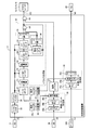
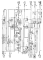
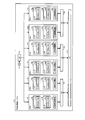
- the CPU 10 includes a core 11, a core 14, and a synchronization control mechanism 17.
- the core 11 has STICK registers 12 and 13 for each strand, and the core 14 similarly has STICK registers 15 and 16 for each strand.
- the CPU 18 includes a core 19, a core 22, and a synchronization control mechanism 25.
- the core 19 has STICL registers 20 and 21, and the core 22 has STICK registers 223 and 24.
- the arbiter 103 also sends a write request and a read request to the STICK registers 13 and 16 to the IU 140 in the same manner.
- the arbiter 103 issues a synchronization request when a program executed by the CPU 10 requests synchronization of processing executed by each of the CPUs 10 to 10b and 18 to 18b, and the route indicated by (L) in FIG. To the synchronization control mechanism 17.
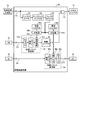
- the synchronization control mechanism 17 includes a synchronizer 30, an up-edge detector 31, a phase counter 32, a setting register 33a, a comparator 33b, a setting register 34a, a comparator 34b, a control packet transmission unit 35, and a control packet reception. Part 36.
- the synchronization control mechanism 17 includes a control register 37, an n pulse generation unit 50, and an AND gate 60.
- the control packet transmission unit 35 includes a transmission buffer 35a, an output circuit 35b, and an encoder 35c.
- the control packet receiving unit 36 includes a decoder 36a, a reception buffer 36b, and an update circuit 36c.
- the output circuit 35b transmits the synchronization request stored in the transmission buffer 35a to the encoder 35c.
- the encoder 35c receives the synchronization request from the output circuit 35b, the encoder 35c generates a control packet storing the synchronization request, and transmits the generated packet to the XB 26 via the path indicated by (M) in FIG. , Broadcast to each of the CPUs 10 to 10b and 18 to 18b. That is, when the synchronization request is issued and the time “XBC Timing” has elapsed since the rising edge of the frequency-divided signal, the control packet transmitter 35 broadcasts the control packet storing the synchronization request.
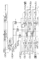
- the core clock of the CPU 10 is set to core clk
- the synchronization signal supplied from the CD 4 is set to stick sync
- the synchronization request input from the application via the arbiter 103 is set to stick ctl req.
- the control signal generated by the n pulse generator 50 is set to stick clk.
- the paths indicated by (K) to (O) in FIG. 5a are the same paths as (K) to (O) shown in FIG.
- the adder # 1 adds 1 to the quotient output from the terminal Q of the divider 53 and inputs the quotient to the multiplexer S2.
- the multiplexer S2 uses the output of the comparator # 0 as the selection control signal, the adder # 1, or The quotient output from the divider 53 is input to the subperiod register 54. That is, the multiplexer S2 corrects the value stored in the sub-period register 54 when the value of the period register 52 is not divisible by N using the output of the comparator # 0.
- the reception buffer 36b holds “0” or “1” which is the packet data output from the decoder.
- the update circuit 36 c is a three-state buffer, and stores the value stored in the reception buffer 36 b in the control register 37 when the comparator 36 c outputs “1”, that is, at “REG-WR Timing”. .
- the value stored in the control register 37 is inverted and input to the AND gate 60. Therefore, when “0” is stored in the control register 37, the stick clk is supplied to the STICK registers 12, 13, 15, and 16, and when “1” is stored in the control register 37, the stick The supply of clk stops.
- the n pulse generation unit 50 continues to output regenerated_stick_clk having a period of eight core clocks. Then, the synchronization control mechanism 17 supplies the pulse signal generated by the n-pulse generator 50 to each of the STICK registers 12, 13, 15, 16 by “REG-WR Timing”.
- the CPUs 10 to 10b, 18 to 18b, the XBs 26 to 26b, and the bus 7 are connected by a serial link whose transmission latency is not constant. For this reason, as shown in FIG. 6, each of the CPUs 10a, 10b, 18 to 18b obtains the control packet at different timings. Also, the CPU 10 acquires the control packet broadcast by itself from the route indicated by (N) in FIG.
- each of the CPUs 10 to 10b and 18 to 18b can simultaneously transmit arbitrary control instructions to the respective CPUs 11 to 18 by using a mechanism for issuing a synchronization request to each of the CPUs 11 to 18. .
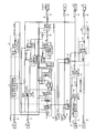
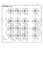
- the CPUs 10c to 10e and 18c to 18e have synchronization control mechanisms 17c to 17e and 25c to 25e.
- the synchronization control mechanisms 17d, 17e, 25c to 25e perform the same processing as the synchronization control mechanism 17c, and the description thereof is omitted.
- the description of XBs 26c to 26h is omitted because they exhibit the same functions as the XB 26 according to the first embodiment.
- the encoder 35g generates a control packet storing the received synchronization signal, and transmits the generated control packet to the synchronization control mechanism 35c via the path shown in (T) of FIG.
- the encoder 35g also transmits the generated packet to the delay circuit 39.
- the packet generated by the encoder 35g is the same packet as the packet generated by the encoder 35c according to the first embodiment.
- the delay circuit 39 outputs the received control packet after a predetermined time has elapsed.
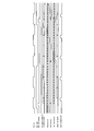
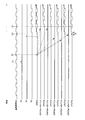
- FIG. 11 is a time chart for explaining the timing for starting the count of the STICK register according to the second embodiment.
- FIG. 11 shows the waveform of the reference signal, the waveform of the stick sync that is the frequency-divided signal obtained from the path shown in FIG. 10 (K), and the frequency of the recycled stick clk generated by the n-pulse generator. Waveform is shown. Further, the waveforms of signals flowing through the paths indicated by (L), (U), (N), and (O) in FIG.
- the synchronization control mechanism 17c receives the control packet output by the delay circuit 39 or the control packet by "XBC Timing" when receiving the control packet from the synchronization control mechanism 25c via (U) in FIG. Is broadcast to the CPUs 10c to 10e.
- the synchronization control mechanism 25c broadcasts a control packet to the CPUs 18c to 18e using the same “XBC Timing” as the synchronization control mechanism 17c.
- the synchronization control mechanism 25c broadcasts the control packet to the CPUs 18c to 18e at the same timing as the synchronization control mechanism 17c broadcasts the control packet.
- the synchronization control mechanism 17c performs the following processing when a predetermined time has elapsed from the up-edge of the frequency-divided signal after receiving the broadcast-transmitted control packet, and becomes “REG-WR Timing”. To do. That is, the synchronization control mechanism 17c supplies a control signal to the STICK registers 12, 13, 15, 16 of the CPU 10c.
- the synchronization control mechanism 17c can appropriately synchronize the processes executed by the CPUs 10c to 10e and 18c to 18e even when the CPUs 10c to 10e and the CPUs 18c to 18e are connected to different buses.
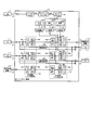
- the setting register 33b is a register for setting “XBC0 Timing”. Specifically, the setting register 33a stores a value indicating the time from the up edge of the frequency-divided signal to “XBC0 Timing” in units of the core clock period. That is, the synchronization control mechanism 17f transmits the control packet to the BC pipeline mechanism 61 of the XB 26i with “XBC0 Timing” instead of “XBC Timing”. Then, when the control packet is received from the BC pipeline mechanism 61 of the XB 26i, the synchronization control mechanism 17f uses the “REG-WR Timing” in the same manner as the synchronization control mechanism 17, and each STICK register 12, 13, 15, Supply of control signals to 16 is started.
- the synchronizer 62, the up-edge detector 63, and the phase counter 64 shown in FIG. 16 will not be described because they perform the same processing as the synchronizer 30, the up-edge detector 31, and the phase counter 32 shown in FIG.
- the setting buffer 65a stores a value indicating how many "XBC0 Timing" are set in the core clock cycle from the up edge of the divided signal.
- FIG. 17 is a diagram for explaining an example of the BC pipeline mechanism.
- the setting registers 65a, 66a, and 67a store values indicating timings of “XBC1 Timing”, “XBC2 Timing”, and “SBC Timing”, respectively, according to the Scan in signal. .
- FIG. 18 is a time chart for explaining the timing at which the synchronization control mechanism transmits a control packet to the BC pipeline mechanism.
- FIG. 18 shows a reference signal, a stick sync, a regenerated stick clk, a signal flowing through the path shown in (L) in FIG. 15, and a signal flowing through the paths shown in (W), (X), and (Y) in FIG. Indicates.
- FIG. 18 shows the timing at which each BC pipeline mechanism 61-61b receives a control packet. In the example shown in FIG.
- the synchronization control mechanism 17 f included in the CPU 10 receives the synchronization request from the application at the timing illustrated in FIG. 18C and transmits the control packet storing the synchronization request to “XBC0 Timing”. Then, the data is transmitted to the BC pipeline mechanism 61. For this reason, the BC pipeline mechanism 61 receives the control packet at the timing shown in FIG. Next, as shown in FIG. 18E, the BC pipeline mechanism 61 executes the following processing when the time elapsed from the up edge of stck sync becomes “XBC1 Timing”.
- the BC pipeline mechanism 61c included in the structural unit 2g, the CPUs 10f to 10h and the CPUs 18f to 18h included in the structural unit 2g indicate timings at which the control packets are received.
- the BC pipeline mechanism 61f, the CPUs 10i to 10k, and the CPUs 18i to 18k included in the structural unit 7i receive the control packets.
- each of the CPUs 10 to 10k and each of the BC pipeline mechanisms 61 to 61f receives the packet at the timing indicated by the dotted line, and each of the CPUs 10 to 10k and each of the BC pipeline mechanisms 61
- the waveforms of the signals received by 61 f are simplified.
- the parallel computer system 1b may include structural units 2f to 2i and 5f to 7i each having an arbitrary number of CPUs.
- the parallel computer system 1b may include structural units 2f to 2i and 5f to 7i each having one CPU. That is, the parallel computer system 1b may have a plurality of CPUs connected in the x-axis direction and the y-axis direction.
- each synchronization control mechanism transmits a synchronization request to the CPU connected in the x-axis direction, and then transmits the synchronization request to the CPU connected in the y-axis direction.
- Each synchronization control mechanism then outputs a synchronization signal to the STICK register of each CPU at the timing indicated by the divided signal.
Landscapes
- Engineering & Computer Science (AREA)
- Theoretical Computer Science (AREA)
- Physics & Mathematics (AREA)
- General Engineering & Computer Science (AREA)
- General Physics & Mathematics (AREA)
- Computer Hardware Design (AREA)
- Mathematical Physics (AREA)
- Software Systems (AREA)
- Computer Networks & Wireless Communication (AREA)
- Signal Processing (AREA)
- Multi Processors (AREA)
Abstract
L'invention concerne un dispositif de commande de synchronisation (17) qui détecte la montée ou la descente d'un signal d'horloge divisé, dans lequel un CD (4) a divisé un signal d'horloge en 1/N périodes. De plus, le dispositif de commande de synchronisation (17) surveille le temps écoulé depuis la montée ou la descente du signal d'horloge divisé de façon à surveiller une seconde heure pour la mise à jour d'un registre STICK (15) détenu par une CPU (10). De plus, le dispositif de commande de synchronisation (17) génère une horloge de commande dans laquelle le signal d'horloge qui a été divisé par le CD (4) est multiplié par N fois. Le dispositif de commande de synchronisation (17) reçoit également des demandes de synchronisation d'autres CPU par le biais d'un XB (26). Le dispositif de commande de synchronisation (17) reçoit ensuite les demandes de synchronisation des autres CPU et, si la seconde heure est détectée, émet l'horloge de commande générée.
Priority Applications (2)
| Application Number | Priority Date | Filing Date | Title |
|---|---|---|---|
| PCT/JP2011/067803 WO2013018218A1 (fr) | 2011-08-03 | 2011-08-03 | Dispositif de commande de synchronisation, dispositif de traitement informatique, système informatique parallèle et procédé de commande de dispositif de commande de synchronisation |
| US14/168,805 US20140146931A1 (en) | 2011-08-03 | 2014-01-30 | Synchronization control apparatus, arithmetic processing device, parallel computer system, and control method of synchronization control apparatus |
Applications Claiming Priority (1)
| Application Number | Priority Date | Filing Date | Title |
|---|---|---|---|
| PCT/JP2011/067803 WO2013018218A1 (fr) | 2011-08-03 | 2011-08-03 | Dispositif de commande de synchronisation, dispositif de traitement informatique, système informatique parallèle et procédé de commande de dispositif de commande de synchronisation |
Related Child Applications (1)
| Application Number | Title | Priority Date | Filing Date |
|---|---|---|---|
| US14/168,805 Continuation US20140146931A1 (en) | 2011-08-03 | 2014-01-30 | Synchronization control apparatus, arithmetic processing device, parallel computer system, and control method of synchronization control apparatus |
Publications (1)
| Publication Number | Publication Date |
|---|---|
| WO2013018218A1 true WO2013018218A1 (fr) | 2013-02-07 |
Family
ID=47628780
Family Applications (1)
| Application Number | Title | Priority Date | Filing Date |
|---|---|---|---|
| PCT/JP2011/067803 WO2013018218A1 (fr) | 2011-08-03 | 2011-08-03 | Dispositif de commande de synchronisation, dispositif de traitement informatique, système informatique parallèle et procédé de commande de dispositif de commande de synchronisation |
Country Status (2)
| Country | Link |
|---|---|
| US (1) | US20140146931A1 (fr) |
| WO (1) | WO2013018218A1 (fr) |
Families Citing this family (5)
| Publication number | Priority date | Publication date | Assignee | Title |
|---|---|---|---|---|
| WO2015182350A1 (fr) * | 2014-05-29 | 2015-12-03 | ソニー株式会社 | Dispositif terminal et procédé |
| GB2597945B (en) * | 2020-08-11 | 2022-11-16 | Graphcore Ltd | Predictive clock control |
| GB202110155D0 (en) | 2021-07-14 | 2021-08-25 | Graphcore Ltd | GSP trace unit |
| GB202110147D0 (en) | 2021-07-14 | 2021-08-25 | Graphcore Ltd | time deterministic trace |
| JP2023084904A (ja) * | 2021-12-08 | 2023-06-20 | 富士通株式会社 | プロセッサ、情報処理装置及び情報処理方法 |
Citations (6)
| Publication number | Priority date | Publication date | Assignee | Title |
|---|---|---|---|---|
| JPH06131074A (ja) * | 1993-05-21 | 1994-05-13 | Hitachi Ltd | 情報処理システム |
| JPH10233766A (ja) * | 1997-02-20 | 1998-09-02 | Advantest Corp | 同期回路 |
| JPH10275038A (ja) * | 1996-10-09 | 1998-10-13 | Fujitsu Ltd | 信号伝送システム、該信号伝送システムのレシーバ回路、および、該信号伝送システムが適用される半導体記憶装置 |
| JP2004536538A (ja) * | 2001-07-26 | 2004-12-02 | モトローラ・インコーポレイテッド | 分散型システムのクロック同期 |
| JP2007050812A (ja) * | 2005-08-19 | 2007-03-01 | Auto Network Gijutsu Kenkyusho:Kk | 負荷制御システム、通信制御ユニットおよび負荷制御方法 |
| WO2011087076A1 (fr) * | 2010-01-14 | 2011-07-21 | 日本電気株式会社 | Système de calcul parallèle, procédé de synchronisation et programme |
Family Cites Families (5)
| Publication number | Priority date | Publication date | Assignee | Title |
|---|---|---|---|---|
| GB2450564B (en) * | 2007-06-29 | 2011-03-02 | Imagination Tech Ltd | Clock frequency adjustment for semi-conductor devices |
| EP2369438B1 (fr) * | 2010-02-24 | 2014-02-26 | Fujitsu Semiconductor Limited | Méthode d'étalonnage d'un signal d'horloge temps réel |
| US8867404B2 (en) * | 2012-02-03 | 2014-10-21 | Futurewei Technologies, Inc. | Node level vectoring synchronization |
| US9288777B2 (en) * | 2012-05-11 | 2016-03-15 | Apple Inc. | Methods and apparatus for synchronizing clock signals in a wireless system |
| US9471091B2 (en) * | 2012-11-28 | 2016-10-18 | Nvidia Corporation | Periodic synchronizer using a reduced timing margin to generate a speculative synchronized output signal that is either validated or recalled |
-
2011
- 2011-08-03 WO PCT/JP2011/067803 patent/WO2013018218A1/fr active Application Filing
-
2014
- 2014-01-30 US US14/168,805 patent/US20140146931A1/en not_active Abandoned
Patent Citations (6)
| Publication number | Priority date | Publication date | Assignee | Title |
|---|---|---|---|---|
| JPH06131074A (ja) * | 1993-05-21 | 1994-05-13 | Hitachi Ltd | 情報処理システム |
| JPH10275038A (ja) * | 1996-10-09 | 1998-10-13 | Fujitsu Ltd | 信号伝送システム、該信号伝送システムのレシーバ回路、および、該信号伝送システムが適用される半導体記憶装置 |
| JPH10233766A (ja) * | 1997-02-20 | 1998-09-02 | Advantest Corp | 同期回路 |
| JP2004536538A (ja) * | 2001-07-26 | 2004-12-02 | モトローラ・インコーポレイテッド | 分散型システムのクロック同期 |
| JP2007050812A (ja) * | 2005-08-19 | 2007-03-01 | Auto Network Gijutsu Kenkyusho:Kk | 負荷制御システム、通信制御ユニットおよび負荷制御方法 |
| WO2011087076A1 (fr) * | 2010-01-14 | 2011-07-21 | 日本電気株式会社 | Système de calcul parallèle, procédé de synchronisation et programme |
Also Published As
| Publication number | Publication date |
|---|---|
| US20140146931A1 (en) | 2014-05-29 |
Similar Documents
| Publication | Publication Date | Title |
|---|---|---|
| WO2013018218A1 (fr) | Dispositif de commande de synchronisation, dispositif de traitement informatique, système informatique parallèle et procédé de commande de dispositif de commande de synchronisation | |
| US8321612B2 (en) | Method and device for synchronizing two bus systems by transmission of a time associated trigger signal from one system to another | |
| US7801131B2 (en) | Method for transmitting data in messages via a communication link of a communication system, as well as a communication module, user of a communication system, and communication system for implementing this method | |
| JP5459807B2 (ja) | マルチプロセッサデータ処理システムにおけるデバッグシグナリング | |
| US7769906B2 (en) | FlexRay communication module | |
| US7328359B2 (en) | Technique to create link determinism | |
| US5787094A (en) | Test and diagnostics for a self-timed parallel interface | |
| JP4903801B2 (ja) | FlexRay通信モジュールとFlexRay加入者装置とを繋ぐ加入者インタフェース、およびFlexRay通信モジュールとFlexRay加入者装置とを繋ぐ加入者インタフェースを経由するメッセージの伝送方法 | |
| US20100005332A1 (en) | Method and system for distributing a global timebase within a system-on-chip having multiple clock domains | |
| US6928528B1 (en) | Guaranteed data synchronization | |
| JP3981192B2 (ja) | Sci相互接続を用いたtocカウンタの同期 | |
| JP3919990B2 (ja) | タイミング同期システム、そのシステムに用いられる装置およびタイミング同期方法 | |
| US8868827B2 (en) | FIFO apparatus for the boundary of clock trees and method thereof | |
| US11442878B2 (en) | Memory sequencer system and a method of memory sequencing using thereof | |
| US11474557B2 (en) | Multichip timing synchronization circuits and methods | |
| JPWO2013018218A1 (ja) | 同期制御装置、演算処理装置、並列計算機システムおよび同期制御装置の制御方法 | |
| US9111042B1 (en) | 1588 deterministic latency with gearbox | |
| US20060023820A1 (en) | Controller for clock synchronizer | |
| US6542999B1 (en) | System for latching first and second data on opposite edges of a first clock and outputting both data in response to a second clock | |
| GB2521035A (en) | A synchronous bridge circuitry and a method of transferring data using asynchronous bridge circuitry | |
| IL304875A (en) | Controlling a network of data processing devices for a quantum computer | |
| Kyriakakis et al. | Implementation of a fault-tolerant, globally-asynchronous-locally-synchronous, inter-chip NoC communication bridge on FPGAs | |
| Hua et al. | HOSA: Holistic scheduling and analysis for scalable fault-tolerant FlexRay design | |
| JP7418159B2 (ja) | 情報処理装置 | |
| JP4788876B2 (ja) | 非同期クロック利用の分散処理同期システム、マスターシステム及びクロック同期制御方法 |
Legal Events
| Date | Code | Title | Description |
|---|---|---|---|
| 121 | Ep: the epo has been informed by wipo that ep was designated in this application |
Ref document number: 11870329 Country of ref document: EP Kind code of ref document: A1 |
|
| ENP | Entry into the national phase |
Ref document number: 2013526697 Country of ref document: JP Kind code of ref document: A |
|
| NENP | Non-entry into the national phase |
Ref country code: DE |
|
| 122 | Ep: pct application non-entry in european phase |
Ref document number: 11870329 Country of ref document: EP Kind code of ref document: A1 |