WO2013011833A1 - Organic light-emitting element, light source device and organic light-emitting element manufacturing method - Google Patents
Organic light-emitting element, light source device and organic light-emitting element manufacturing method Download PDFInfo
- Publication number
- WO2013011833A1 WO2013011833A1 PCT/JP2012/066996 JP2012066996W WO2013011833A1 WO 2013011833 A1 WO2013011833 A1 WO 2013011833A1 JP 2012066996 W JP2012066996 W JP 2012066996W WO 2013011833 A1 WO2013011833 A1 WO 2013011833A1
- Authority
- WO
- WIPO (PCT)
- Prior art keywords
- dopant
- light emitting
- organic light
- emitting layer
- emitting device
- Prior art date
Links
Images


Classifications
-
- H—ELECTRICITY
- H10—SEMICONDUCTOR DEVICES; ELECTRIC SOLID-STATE DEVICES NOT OTHERWISE PROVIDED FOR
- H10K—ORGANIC ELECTRIC SOLID-STATE DEVICES
- H10K50/00—Organic light-emitting devices
- H10K50/80—Constructional details
- H10K50/805—Electrodes
-
- H—ELECTRICITY
- H10—SEMICONDUCTOR DEVICES; ELECTRIC SOLID-STATE DEVICES NOT OTHERWISE PROVIDED FOR
- H10K—ORGANIC ELECTRIC SOLID-STATE DEVICES
- H10K71/00—Manufacture or treatment specially adapted for the organic devices covered by this subclass
- H10K71/10—Deposition of organic active material
- H10K71/191—Deposition of organic active material characterised by provisions for the orientation or alignment of the layer to be deposited
-
- H—ELECTRICITY
- H10—SEMICONDUCTOR DEVICES; ELECTRIC SOLID-STATE DEVICES NOT OTHERWISE PROVIDED FOR
- H10K—ORGANIC ELECTRIC SOLID-STATE DEVICES
- H10K50/00—Organic light-emitting devices
- H10K50/80—Constructional details
- H10K50/85—Arrangements for extracting light from the devices
- H10K50/856—Arrangements for extracting light from the devices comprising reflective means
-
- H—ELECTRICITY
- H10—SEMICONDUCTOR DEVICES; ELECTRIC SOLID-STATE DEVICES NOT OTHERWISE PROVIDED FOR
- H10K—ORGANIC ELECTRIC SOLID-STATE DEVICES
- H10K50/00—Organic light-emitting devices
- H10K50/80—Constructional details
- H10K50/85—Arrangements for extracting light from the devices
- H10K50/858—Arrangements for extracting light from the devices comprising refractive means, e.g. lenses
-
- H—ELECTRICITY
- H10—SEMICONDUCTOR DEVICES; ELECTRIC SOLID-STATE DEVICES NOT OTHERWISE PROVIDED FOR
- H10K—ORGANIC ELECTRIC SOLID-STATE DEVICES
- H10K71/00—Manufacture or treatment specially adapted for the organic devices covered by this subclass
-
- H—ELECTRICITY
- H10—SEMICONDUCTOR DEVICES; ELECTRIC SOLID-STATE DEVICES NOT OTHERWISE PROVIDED FOR
- H10K—ORGANIC ELECTRIC SOLID-STATE DEVICES
- H10K85/00—Organic materials used in the body or electrodes of devices covered by this subclass
- H10K85/30—Coordination compounds
- H10K85/341—Transition metal complexes, e.g. Ru(II)polypyridine complexes
- H10K85/346—Transition metal complexes, e.g. Ru(II)polypyridine complexes comprising platinum
Definitions
- the present invention relates to an organic light emitting device, a light source device, and a method for manufacturing the organic light emitting device.
- Patent Document 1 discloses the following technique. That is, for the purpose of providing an organic electroluminescent device having improved luminous efficiency by “orienting organic molecules constituting the light emitting layer in parallel with the light emitting surface”, light emission comprising an organic compound in the anode electrode layer and the cathode electrode layer.
- An organic electroluminescence device comprising a plurality of layers, wherein the light emitting layer is formed by a dry process in a vacuum, and the organic compound molecules constituting the light emitting layer are oriented parallel to the surface direction of the light emitting layer This is an organic EL light emitting device.
- Patent Document 2 discloses the following technique.
- the purpose is to reduce or eliminate the occurrence of various defective modes, and “Organic molecules constituting the light emitting layer are perpendicular to the light emitting surface.
- the organic thin film EL device is characterized in that organic compound molecules are oriented in accordance with the direction of current flow.
- Non-Patent Document 1 discloses the following technology. That is, for the purpose of improving the luminous efficiency of the organic light-emitting device, the energy of the surface plasmon polariton is reduced by forming a two-dimensional nanostructure on the metal electrode adjacent to the “light emitting layer not specifically controlled”.
- the organic thin film EL device is characterized by being converted into visible light.
- Patent Document 3 discloses the following technique. That is, for the purpose of extracting light from the light emitting layer to the outside with high efficiency, an organic material layer including at least one light emitting layer made of an organic EL material is disposed between the first electrode layer and the second electrode layer.
- the metal fine particles are disposed inside the dielectric.
- the organic thin film EL device further includes a metal fine particle layer dispersed in the metal fine particle layer, and the metal fine particles of the metal fine particle layer excite plasmon resonance when the light propagates in the metal fine particle layer.
- Patent Document 1 the configuration and orientation control method described in Patent Document 1 have problems that the manufacturing process is complicated and the film formation rate is slow.
- increasing the number of horizontally oriented organic molecules cannot reduce non-radiative recombination of electron-hole pairs except for excitation of surface plasmon polaritons, so there is a limit to improving internal quantum efficiency, and the final emission There are limits to improving efficiency.
- Non-Patent Document 1 a part of the energy consumed for excitation of the surface plasmon polariton can be converted into visible light, but since the orientation control of the organic molecules in the light emitting layer is not particularly performed, The energy of the horizontally oriented organic molecule cannot be extracted because it does not transfer to the surface plasmon polariton. Further, the energy of the horizontally oriented organic molecules is partly spent on non-radiative recombination of electron-hole pairs excluding the excitation of surface plasmon polaritons. As described above, the effect of improving the luminous efficiency is limited.
- Patent Document 3 Furthermore, in the configuration of Patent Document 3, a high-resistance dielectric layer is sandwiched between the electrodes, and it is difficult to perform efficient current injection. Therefore, there is a limit to improving the light emission efficiency.
- the object of the present invention is to reduce the influence of non-radiative recombination of electron-hole pairs other than excitation of surface plasmon polaritons and improve internal quantum efficiency, that is, convert most of exciton energy into visible light, This is to drastically improve the luminous efficiency of the organic light emitting device.
- the conventional alignment control method has problems that the manufacturing process is complicated and the film forming speed is slow, and the present invention provides a method for manufacturing an organic light emitting device including an effective alignment control method.
- the organic light-emitting device of the present invention has a lower electrode and an upper electrode, one of which is a reflective electrode and the other is a transparent electrode, which is disposed between the lower electrode and the upper electrode, A light emitting layer containing a dopant, wherein the first dopant includes a first functional group, and the first dopant has an average value of a transition dipole moment with respect to a substrate plane and a horizontal component.
- the organic light emitting device of the present invention is an organic light emitting device having a reflective electrode, a transparent electrode, and a light emitting layer disposed between the reflective electrode and the transparent electrode.
- the organic light emitting device of the present invention is an organic light emitting device having an upper electrode, a lower electrode, and a light emitting layer disposed between the upper electrode and the lower electrode.
- the first dopant includes a first functional group, the concentration of the first dopant, the region on the side where the upper electrode exists in the light emitting layer, and the lower portion Either one of the regions where the electrodes are present is higher than the other region, and the horizontal component of the average value of the transition dipole moment with respect to the substrate surface is greater than the vertical component for the first dopant.
- the effect of the present invention is that the effect of non-radiative recombination of electron-hole pairs excluding excitation of surface plasmon polariton can be reduced, and most of exciton energy can be converted into visible light, thereby improving the luminous efficiency of the organic light-emitting device.
- Another effect of the present invention is to provide an organic light-emitting element, a light source device, and a method for manufacturing the organic light-emitting element, in which highly efficient light emission can be obtained by controlling the orientation of dopant molecules by a simple method. .
- Organic light-emitting devices are promising technologies for displays, light sources, and lighting devices.
- the electrical energy obtained from an external power source forms excitons (electron-hole pairs) in the organic molecules of the light-emitting layer in the organic light-emitting device, and the excitons relax (electron-hole pairs bind)
- the surplus energy becomes visible light, and this visible light is emitted from the device to the air.
- the energy of organic molecules is not efficiently converted into light in the organic light emitting device, and thus the light extraction efficiency to the outside is reduced.
- the mechanism that prevents the conversion of the excited organic molecules into visible light is as follows.
- a light emitting layer often exists within 250 nm from a metal electrode.
- excitons that is, electric dipoles exist near the surface of the metal electrode.
- the evanescent waves contained in the radiation field of the electric dipole and the reflection field on the metal surface interact with each other in the near field. Due to this near-field interaction, the electric dipole energy flows into the metal as tunnel energy and is consumed by the excitation energy of the metal surface plasmon polariton.
- the excitation energy of surface plasmon polaritons dissipates as Joule heat due to the finite lifetime of surface plasmon polaritons.
- the energy consumed for excitation of the surface plasmon polariton is about 25% of the exciton energy.
- the direction of the transition dipole moment in the organic molecule can be controlled by the molecular skeleton. For example, if all atoms constituting a molecule are in the same plane (on the plane), the transition dipole moment also has a direction in the molecule plane. Moreover, the direction of the transition dipole moment can also be controlled by making the arrangement of some atoms in the molecule where the electron-hole pairs involved in the transition are distributed in the same plane. In this case, it is not necessary that all atoms constituting the molecule are in the same plane.
- the transition dipole moment indicates a transition moment that is a non-diagonal element among the transition dipole matrix elements constituting the electric dipole transition of the molecule, and its absolute value is proportional to the oscillator strength.
- transition dipole moment in the present invention means an average transition dipole moment of transition related to light emission of the organic light emitting device.
- nano-concave structure that converts surface plasmon polariton energy into visible light when a nano-concave structure that converts surface plasmon polariton energy into visible light is not provided, a device configuration in which the light emission efficiency is reduced (or organic molecules in the light emitting layer are vertically aligned) is formed, and then the surface plasmon polariton energy is reduced.
- the limitations of providing nano-concave structures that convert surface plasmon polariton energy into visible light in a conventional device configuration organic molecules in the light-emitting layer is isotropic (random) orientation
- FIG. 1 is a cross-sectional view of an embodiment of a light source unit of a light source device according to the present invention.
- FIG. 1 shows a top emission type light source device that extracts light from the upper electrode 102 side.
- the lower electrode 101, the first bank 104, the second bank 105, the organic layer 103, the upper electrode 102, the resin layer 106, the sealing substrate 107, and the light extraction layer 108 are arranged on the substrate 100 in the above order.
- a light source device is provided by including a drive circuit and a housing not shown in FIG.
- the organic light emitting device is a portion having an upper electrode 102, a lower electrode 101, and an organic layer 103.
- the lower electrode 101 is an anode, but the lower electrode 101 may be a cathode.
- the lower electrode 101 is formed by patterning by photolithography.
- the upper electrode 102 When the lower electrode 101 is an anode, the upper electrode 102 is a cathode. When the lower electrode 101 is a cathode, the upper electrode 102 is an anode.
- the upper electrode 102 When the upper electrode 102 is ITO or IZO, when ITO or IZO is formed by sputtering, a buffer layer may be provided between the organic layer 103 and the upper electrode 102 in order to reduce damage caused by sputtering. A metal oxide such as molybdenum oxide or vanadium oxide is used for the buffer layer.
- the upper electrode 102 is connected to the lower electrode 101 of the adjacent light emitting unit. Thereby, a light emission part can be connected in series.
- the first bank 104 formed on the side surface of the organic light emitting device has a forward taper, covers the end of the patterned lower electrode 101, and prevents a partial short-circuit failure of the light emitting portion.
- the first bank 104 is formed by developing and exposing using a predetermined photomask.
- the surface of the first bank 104 on the side where the organic layer 103 is present may be subjected to water repellency treatment.
- the surface of the first bank 104 is subjected to a plasma treatment with a fluorine-based gas, and the surface of the first bank 104 is fluorinated to perform the water repellency treatment. Thereby, a water repellent layer is formed on the surface of the first bank 104.
- Photosensitive polyimide is preferable as the first bank 104.
- an acrylic resin, a novolac resin, a phenol resin, a non-photosensitive material, or the like can be used.
- the second bank 105 is formed on the first bank 104.
- the second bank 105 has a reverse taper and is used to prevent the upper electrode 102 of the adjacent light emitting portion from conducting.
- the second bank 105 is formed by developing and exposing using a predetermined photomask.
- the surface of the second bank 105 on the side where the organic layer 103 is present may be subjected to water repellency treatment.
- the surface of the second bank 105 is subjected to a plasma treatment with a fluorine-based gas, and the surface of the second bank 105 is fluorinated to perform the water repellency treatment.
- a water repellent layer is formed on the surface of the second bank 105.
- It is preferable to use a negative photoresist as the second bank 105.
- an acrylic resin, a novolac resin, a phenol resin, a non-photosensitive material, or the like can be used.
- the resin layer 106 is formed on the upper electrode 102 and the second bank 105.
- the resin layer 106 is used to seal the light emitting portion and prevent intrusion of gas and moisture that cause deterioration of the light emitting element.
- various polymers such as an epoxy resin can be used.
- an inorganic passivation film on the upper electrode 102 can be used as the resin layer 106.
- the sealing substrate 107 is formed on the resin layer 106.
- the sealing substrate 107 is a glass substrate. However, other than the glass substrate, a plastic substrate having an appropriate gas barrier film can also be used.
- the light extraction layer 108 is formed on the sealing substrate 107.
- the light extraction layer 108 is used for efficiently extracting light emitted from the organic layer 103.
- a structure such as a microlens, or a film having scattering properties and diffuse reflection properties is used.
- the organic light emitting element used here may be a single element or an element divided into a plurality of elements. Examples of a method of connecting a plurality of elements include a method in which each element is connected in series, in parallel, or a combination thereof. Further, when the organic light emitting element is divided into a plurality of parts, the following modes are conceivable.
- the first dopant, the second dopant, and the third dopant will be described later.
- (1) There are a plurality of single organic light emitting devices including a first dopant, a second dopant, and a third dopant.
- FIG. 2 is a cross-sectional view of an embodiment of the organic light-emitting device according to the present invention.
- the organic layer 103 may have a single layer structure including only the light emitting layer 303 or a multilayer structure including one or more of the electron injection layer 305, the electron transport layer 304, the hole transport layer 302, and the hole injection layer 301.
- the electron injection layer 305 and the electron transport layer 304, the electron transport layer 304 and the light emitting layer 303, the light emitting layer 303 and the hole transport layer 302, the hole transport layer 302 and the hole injection layer 301 may be in contact with each other.
- Other layers described above may be interposed between the two layers.
- the light emitting layer 303 includes host molecules (hereinafter referred to as “host”) and dopant molecules (hereinafter referred to as “dopant”).
- the light source unit including the organic light emitting element in FIG. 1 is provided with a drive circuit, a housing, and the like, thereby forming a light source device.
- FIG. 3 is a schematic perspective view of an embodiment of a light source device according to the present invention.
- the first organic light emitting element 202 and the second organic light emitting element 203 are divided by the second bank 105.
- a diffusion plate 201 is disposed in a direction in which light is extracted from the first organic light emitting element 202 and the second organic light emitting element 203.
- the first organic light emitting device 202 is an organic light emitting device including a red dopant and a green dopant
- the second organic light emitting device 203 is an organic light emitting device including a blue dopant.
- the configuration of (3) above in FIG.
- the first organic light emitting device 202 and the second organic light emitting device 203 include an organic light emitting device containing a red dopant, an organic light emitting device containing a green dopant, and a blue dopant. It becomes either of the organic light emitting element containing.
- the arrangement of the organic light emitting elements may be a staggered pattern as well as a stripe pattern as shown in FIG. When the organic light emitting device is produced by coating, it can be easily produced by arranging the organic light emitting devices in a stripe shape as shown in FIG.
- a diffusion plate 201 may be attached to the upper part of the light extraction surface of the organic light emitting element as shown in FIG.
- a scatterer dispersed in a resin or glass, a concavo-convex structure formed on the surface, or the like can be considered.
- the blue dopant has a maximum PL spectrum intensity between 400 nm and 500 nm at room temperature (25 ° C.).
- the green dopant has a maximum PL spectrum intensity at room temperature between 500 nm and 590 nm.
- the red dopant 5 has the maximum intensity of the PL spectrum at room temperature between 590 nm and 780 nm.
- a fluorescent dopant and a phosphorescent dopant skeleton added with a functional group can be used.
- Examples of the fluorescent dopant skeleton include planar molecules that are condensed polycyclic aromatic compounds such as perylene, naphthalene, anthracene, pyrene, phenanthrene, pentacene, tetracene, chrysene, coumarin, coronene, perinone, and derivatives thereof.
- Examples of the phosphorescent dopant skeleton include metal porphyrin derivatives and tetracoordinate metal complexes represented by the general formula (1) of (Chemical Formula 1).
- N-L1-X1 and X2-L2-X3 each represent a bidentate ligand, and X1, X2, and X3 each independently represent a carbon atom, an oxygen atom, or a nitrogen atom.
- L1 and L2 are N represents an atomic group forming a bidentate ligand with X1, X2, and X3, and the central metal M represents Ni, Pd, Pt, Au, Ag, Rh, and Ir.
- L1 in the general formula (1) Is a condensed polycyclic aromatic derivative such as benzoquinoline or phenanthroline, or a compound represented by the general formula (2) of (Chemical Formula 2).
- Examples of the aromatic heterocycle represented by Y1 include quinoline ring, isoquinoline ring, pyridine ring, quinoxaline ring, thiazole ring, pyrazole ring, pyrimidine ring, benzothiazole ring, oxazole ring, benzoxazole ring, indole ring, isoindole ring, etc. Can be given.
- aromatic hydrocarbon ring or aromatic heterocycle represented by Y2 in addition to the aromatic heterocycle in Y1, benzene ring, naphthalene ring, anthracene ring, thiophene ring, benzothiophene ring, furan ring, benzofuran ring, Examples thereof include a fluorene ring and a benzopyran ring. Substituents other than functional groups may be added to the aromatic heterocycle or aromatic hydrocarbon ring.
- substituents examples include an alkyl group (methyl group, ethyl group), a substituted alkyl group (trifluoromethyl group), an alkoxy group (methoxy group), a halogen atom (fluorine, chlorine), an amino group, and a phenyl group.
- L2 in the general formula (1) may be contained in L1, but other examples include acetylacetonate derivatives, picolinate derivatives, and tetrakispyrazolyl borate derivatives.
- the solid concentration of the blue dopant is desirably 10 wt% or more and 30 wt% or less, the solid content of the green dopant is desirably less than 10 wt%, and the solid content of the red dopant is desirably less than 10 wt%.
- the weight average molecular weight of the luminescent dopant is preferably 500 or more and 3000 or less.
- the luminescent dopant molecule has various shapes such as a planar shape, a rod shape, a regular tetrahedral shape, a regular octahedral shape, and a spherical shape. By adding an appropriate functional group to these molecules, it can be oriented substantially perpendicular to the substrate surface. By orienting the molecules, the orientation of the transition dipole moment is controlled.
- Oriented substantially vertically means that the vertical component of the average value of molecules with respect to the substrate surface is larger than the horizontal component.
- the vertical component of the average value of the planar molecules with respect to the substrate surface is larger than the horizontal component.
- the vertical component of the average value of the long axes of the rod-like molecules with respect to the substrate surface is larger than the horizontal component.
- the planar molecule is, for example, the above-mentioned condensed polycyclic aromatic compound, the tetracoordinate metal complex represented by the general formula (1), or the rod-like molecule is an aspect ratio (short side length to short side length). (Side / long side) is in the range of 0.05 to 0.3.
- a planar molecule or rod-like molecule that is a luminescent dopant By adding an appropriate functional group to a planar molecule or rod-like molecule that is a luminescent dopant, it can be oriented substantially perpendicular to the substrate surface.
- a functional group is added to one or both of the bidentate ligands L1 and L2.
- the functional group those having a small surface energy or those having a large interaction with the underlayer are preferable.
- a functional group having a low surface energy is a fluoroalkyl group, a perfluoroalkyl group, an alkyl group (however, the number of C is 10 or more), perfluoro, and the like. Examples thereof include a polyether group and a siloxy group (—Si—O—Si—).
- a fluoroalkyl group and a perfluoropolyether group are desirable, and a perfluoroalkyl group is more desirable.
- the substituent having fluorine the larger the number of fluorine, the stronger the action of moving to the film surface.
- the number of fluorines present in the substituent is desirably 7 or more.
- These groups may be directly introduced into the main skeleton as in (Chemical Formula 3), but in consideration of the bond angle, it is more preferable to introduce them through an amide bond or an ester bond as in (Chemical Formula 4).
- a functional group having a large interaction with the underlayer a functional group having a similar structure to an underlayer (such as a hole transport layer or an electron transport layer) such as a phenylamino group, an oxazole group, a carbazole group, or a hydrazone site, Hydroxy group (—OH), thiol group (—SH), carboxyl group (—COOH), sulfo group (—SO 3 H), I, Br, Cl, F, SCN, CN, NH 2 , NO 2 , bipyridyl group Can be given.
- These groups may be directly introduced into the main skeleton as in (Chemical Formula 5), but are preferably introduced via an alkyl chain in consideration of the size and bond angle of the molecule.
- the functional group is added to one end of the molecule.
- a functional group is added to only one ligand as shown in (Chemical Formula 6).
- a functional group having a low surface energy is added to one end of the rod-like molecule and a functional group having a strong interaction with the underlayer is added to the other end.
- planar molecules add a functional group with low surface energy to one ligand as shown in (Chemical Formula 7), and add a functional group that strongly interacts with the underlying layer to the other ligand. Is preferred.
- the surface of a substance is generally unstable because of the absence of the same kind of molecules on one side and no attractive force. Therefore, a force (surface tension) for deforming the surface area to reduce the surface energy acts.
- a force surface tension
- the surface energy is lowered and stabilized by exposing the functional group to the surface.
- the surfactant has a hydrophobic group, which is a functional group having a low surface energy, in the molecule, and the single molecule on the surface of the water in the form of releasing the hydrophobic group from the water surface. The surface energy of the water surface is reduced by forming a film.
- the molecule of the present invention has a functional group with low surface energy such as a fluoroalkyl group in the molecule. Sites such as the benzene ring have higher surface energy.
- a force acts to bring out the functional group having a low surface energy on the surface in order to reduce the surface energy.
- the molecular surface can be oriented almost perpendicularly to the substrate surface by moving a functional group having a low surface energy to the film surface by this action.
- the functional group is attracted to the underlayer by the action of intermolecular force, hydrogen bond, and coordinate bond acting between the underlayer and the functional group.
- a functional group is added as in (Chemical Formula 5)
- the molecular plane can be oriented almost perpendicularly to the substrate surface by this action.
- the orientation state can be examined by measuring the IR spectrum or the Raman spectrum while changing the incident angle.
- the orientation state of the organic molecule can be examined by measuring the IR spectrum or the Raman spectrum while changing the incident angle.
- the direction of the transition dipole moment can be evaluated by a known method. For example (APPLIED PHYSICS LETTERS 96,073302 (2010).), Using the hemispherical lens / cylindrical lens optically contacting the organic light-emitting device to determine the radiation angle dependence of the P-polarized component of photoluminescence Then, the ratio of each of the horizontal component and the vertical component in the transition dipole moment can be obtained by experimental measurement and comparison with computer simulation. This is because the angle dependence of the P-polarized light intensity is determined by the ratio between the horizontal component and the vertical component (S-polarized light consists of only the horizontal component). The orientation of the organic molecules constituting the normal light emitting layer is random (isotropic), and therefore the proportion of the constituent components of the transition dipole moment is 50% for both the horizontal component and the vertical component.
- ⁇ Host> As the host, it is preferable to use a carbazole derivative, a fluorene derivative, an arylsilane derivative, or the like. In order to obtain efficient light emission, it is preferable that the excitation energy of the host is sufficiently larger than the excitation energy of the blue dopant. The excitation energy is measured using an emission spectrum.
- the hole injection layer 301 is used for the purpose of improving luminous efficiency and lifetime. Moreover, although it is not essential, it is used for the purpose of relaxing the unevenness of the anode.
- the hole injection layer 301 may be provided as a single layer or a plurality of layers.
- the hole injection layer 301 is preferably a conductive polymer such as PEDOT (poly (3,4-ethylenedioxythiophene)): PSS (polystyrene sulfonate).
- PEDOT poly (3,4-ethylenedioxythiophene)
- PSS polystyrene sulfonate
- polypyrrole-based or triphenylamine-based polymer materials can be used.
- phthalocyanine compounds and starburst amine compounds that are often used in combination with a low molecular weight (weight average molecular weight 10,000 or less) material system are also applicable.
- the hole transport layer 302 is made of a material having a function of transporting holes. In a broad sense, the hole injection layer 301 and the electron blocking layer are also included in the hole transport layer.
- the hole transport layer 302 may be provided as a single layer or a plurality of layers.
- a starburst amine compound, a stilbene derivative, a hydrazone derivative, a thiophene derivative, or the like can be used. Further, the present invention is not limited to these materials, and two or more of these materials may be used in combination.
- the electron transport layer 304 is a layer that supplies electrons to the light emitting layer 303.
- the electron injection layer 305 and the hole blocking layer are also included in the electron transport layer 304.
- the electron transport layer 304 may be provided as a single layer or a plurality of layers. Examples of the material for the electron transport layer 304 include bis (2-methyl-8-quinolinolato) -4- (phenylphenolato) aluminum (hereinafter referred to as BAlq) and tris (8-quinolinolato) aluminum (hereinafter referred to as Alq3).
- Tris (2,4,6-trimethyl-3- (pyridin-3-yl) phenyl) borane hereinafter 3TPYMB
- 1,4-Bis (triphenylsilyl) benzene hereinafter UGH2
- oxadiazole derivative 1,4-Bis (triphenylsilyl) benzene
- triazole Derivatives fullerene derivatives, phenanthroline derivatives, quinoline derivatives, and the like can be used.
- the electron injection layer 305 improves the electron injection efficiency from the cathode to the electron transport layer 304.
- lithium fluoride, magnesium fluoride, calcium fluoride, strontium fluoride, barium fluoride, magnesium oxide, and aluminum oxide are desirable.
- the material is not limited to these materials, and two or more of these materials may be used in combination.
- Examples of the substrate 100 include a glass substrate, a metal substrate, a plastic substrate on which an inorganic material such as SiO 2 , SiNx, and Al 2 O 3 is formed.
- Examples of the metal substrate material include alloys such as stainless steel and 42 alloy.
- Examples of the plastic substrate material include polyethylene terephthalate, polyethylene naphthalate, polymethyl methacrylate, polysulfone, polycarbonate, and polyimide.
- the anode material any material having transparency and a high work function can be used. Specifically, conductive oxides such as ITO and IZO and metals having a large work function such as thin Ag can be used.
- the electrode pattern can be formed on a substrate such as glass by using photolithography.
- the cathode needs to have an uneven structure capable of inducing and scattering surface plasmon polaritons. Since the maximum height, width, and pitch of the unevenness may be smaller than the emission wavelength, 5 nm or more and 800 nm or less are desirable. Since the emission wavelength is visible light, it is in the range of 380 nm to 800 nm. In addition, when the size of the unevenness is smaller than 10 nm, it becomes difficult to produce, the cost is increased, and the wavelength shorter than the visible region is amplified. If it is larger than 800 nm, it becomes difficult to scatter visible light. Such a film is referred to herein as a plasmon extraction nanostructure.
- a granular film having a granular surface or an island-shaped structure film in which metal fine particles are dispersed non-periodically or in a periodic arrangement pattern in a film shape and voids exist between the fine particles is preferable. Since the cathode is an island-shaped structure film, the surface plasmon polariton induced in the cathode by the emitted light is converted again to visible light, and the internal quantum efficiency and the luminous efficiency are improved.
- the cathode material Al, Ag, Au, Cu, a laminate of LiF and Al, an Mg: Ag alloy, or the like is preferably used. Moreover, it is not limited to these materials, For example, a Cs compound, Ba compound, Ca compound etc. can be used instead of LiF.
- the height of the plasmon extraction nanostructure is preferably 40 nm to 120 nm so that the near field formed by the excited organic molecule and the surface plasmon polariton resonance are strongly generated. In terms of materials, it is more desirable that the near-field generated by the excited organic molecule and the surface plasmon polariton resonance are strong, and an alloy containing any one of Ag, Au, Cu and Al as a main component (80% or more). Is applicable.
- Ag is desirable when the emitted light is a visible wavelength. This is because Ag can cause surface plasmon resonance in the visible range from the plasma frequency. If the emitted light has a wavelength other than the visible range, for example, infrared, Au is desirable.
- the organic light emitting element as described above is configured, for example, so that it is sequentially stacked on the substrate from the cathode side, and light is extracted from the anode side.
- the cathode can be formed using, for example, a sputtering method, a vacuum evaporation method, or the like.
- the plasmon extraction nanostructure can be prepared by subjecting the cathode to known photolithography or embossing using a roll. In addition, by forming irregularities of the same size as the plasmon extraction nanostructure on the base substrate, and forming a light emitting layer etc. on it, the plasmon extraction nanostructure is formed in a form that reflects the irregularities of the underlying layer on the upper layer. May be.
- metal nanoparticles having such a size that plasmon can be extracted may be applied on a flat metal electrode.
- the gold back nanoparticles may be immobilized on the metal electrode using SAM (self-assembled monolayer).
- SAM self-assembled monolayer
- a nanosphere having a diameter of about 100 nm such as polystyrene, may be applied to and deposited on a substrate, and a metal may be vapor-deposited on the nanosphere to produce a structure in which a metal thin film is deposited on the top of the nanosphere.
- the lifetime of surface plasmon polariton excitation and visible light scattering is generally faster than the normal luminescence and non-radiative recombination rates, and therefore, by measuring the luminescence lifetime, surface plasmon polariton can be obtained. It can be confirmed that the light is emitted through the.
- the organic light emitting device includes a bottom emission type in which light from the organic layer is extracted from the substrate side (side with the transparent electrode) as a substrate / transparent electrode (anode) / organic layer / reflecting electrode (cathode), and a substrate / reflecting electrode (cathode).
- a substrate / transparent electrode (anode) / organic layer / reflecting electrode (cathode) is a top emission type in which light emitted from the organic layer is extracted from the side opposite to the substrate (the side with the transparent electrode).
- the transparent electrode (anode) is the lower electrode
- the reflective electrode (cathode) is the upper electrode.
- the reflective electrode (cathode) is the lower electrode and the transparent electrode (anode) is the upper electrode.
- the transparent electrode anode
- the top emission type it is important to provide a plasmon extraction nanostructure on the lower electrode.
- the coating liquid is obtained by dissolving the material forming the light emitting layer 303 in an appropriate solvent.
- a host, a red dopant, a green dopant, and a blue dopant can be included as a material for forming the light emitting layer 303 will be described.
- the solvent used here may be any solvent that can dissolve each material such as an aromatic hydrocarbon solvent such as toluene, an ether solvent such as tetrahydrofuran, alcohols, and a fluorine solvent.
- a mixed solvent in which a plurality of the above-mentioned solvents are mixed for adjusting the solubility of each material and the drying speed may be used.
- two types of solvents having different boiling points first solvent and second solvent
- the second solvent having a high boiling point is used as a solvent for the green or blue dopant.
- the movement to the film surface can be promoted.
- the solubility of the solvent is measured by a liquid chromatogram method.
- the light emitting layer 303 is formed by a dry method such as a vacuum deposition method, and as a wet method (coating method), a spin coating method, a casting method, a dip coating method, a spray coating method, a screen printing method, an ink jet printing method, a slot Examples thereof include a die coating method, a gravure coating method, and a bar coating method.
- the light emitting layer 303 is formed using one of these methods.
- the coating method has advantages such as easy formation of a large area and high material utilization efficiency.
- advantages such as easy formation of a large area and high material utilization efficiency.
- a white light emitting device having the structure shown in FIG. 4 was produced.
- the substrate 100 was produced as follows. Photoresist (manufactured by Tokyo Ohka: THMR-iP3300) is coated on a quartz substrate, and two-photon interference fringes by He-Cd laser (wavelength: 325 nm) are changed by 60 ° angle, developed after double exposure, and reacted. The substrate was etched by reactive ion etching, and then the photoresist was removed to form irregularities on the substrate. At this time, the depth of the unevenness was 70 nm, and the pitch of the unevenness was 420 nm. By forming a film on this substrate as described below, an organic light-emitting device can be formed while maintaining the unevenness of the substrate, and the finally deposited Al film also reflects the unevenness of the underlying plasmon extraction nanostructure Can be produced.
- the light-emitting layer 303 includes mCP (1,3-bis (carbazol-9-yl) benzene) as a host, (Chemical formula 7) for a blue dopant, (Chemical formula 3) for a red dopant, and (Chemical formula 6) for a green dopant. Using. The emission wavelength of the blue dopant is 460 nm. The weight ratio of each material was 100: 10: 0.5: 0.5.
- Comparative Example 1-1 an element using a dopant that does not add a functional group was produced
- Comparative Example 1-2 an element in which a plasmon extraction nanostructure was not produced on a quartz substrate was produced.
- the configuration of Comparative Example 1-2 is shown in FIG. Assuming that the luminous efficiency of Comparative Example 1-1 is 1, Example 1 shows a luminous efficiency 1.31 times higher, and the luminous efficiency of Comparative Example 1-2 was 0.15 times that of Comparative Example 1-1. .
- Example 1 when a light emitting layer having the same configuration as that of Example 1 was separately prototyped, and the photoluminescence measurement was performed to measure the angle dependency of the P-polarized light intensity, and the proportion of the constituent components of the transition dipole moment of each color dopant was examined, The vertical component of each color was 95%. On the other hand, in Comparative Example 1-1, the horizontal component of each color was 50%. Since Comparative Example 1-2 used a dopant with a functional group added, the vertical component of each color was 95% as in Example 1.
- Example 1 when the direction of the transition dipole moment is isotropic, about 75% of the exciton energy is converted into visible light, and 25% is derived from the surface plasmon polariton. Loss. Therefore, in contrast to Comparative Example 1-1 in which the direction of the transition dipole moment is isotropic, the light emission efficiency of Example 1 in which the direction of the transition dipole moment is substantially perpendicular and has a plasmon extraction nanostructure is 1. 31 ( ⁇ (25 + 75) /75 ⁇ 1.33) times is considered that most of the loss due to the surface plasmon polariton was converted to visible light by the plasmon extraction nanostructure, and the upper limit for improving efficiency A close enough large value.
- Example 1 the emission lifetime was measured as follows. Nitrogen laser light (wavelength 337 nm, pulse width 1 ns) was irradiated to each element as excitation light, and the light emission lifetime from each light emitting material was measured with a streak camera (C4334 manufactured by Hamamatsu Photonics). As a result, the emission lifetime of Example 1 was 24 ns, whereas that of Comparative Example 1-1 was 30 ns, and that of Comparative Example 1-2 was 624 ns. Therefore, in Example 1 and Comparative Example 1-2, it is considered that light emission via surface plasmon polaritons is observed. In particular, in Example 1, the effect of improving the light emission efficiency by the plasmon extraction nanostructure is larger than that in Comparative Example 1-2.
- a light source device in which a plurality of organic light emitting elements were connected was produced.
- the fabricated device has the same substrate and layer structure as in Example 1, with the light-emitting layer containing a host and a red dopant (Chemical Formula 3), and a green dopant (Chemical Formula 5) and a light-emitting layer with a host.
- An element (B element) containing (chemical formula 4) as a blue dopant was formed in-plane, and each element was connected in series and in parallel.
- the emission wavelength of the blue dopant is 450 nm.
- An inkjet method was used for producing the coating film.
- each color dopant was set to be around 75 nm from the upper electrode (reflection electrode). In order to obtain uniform white light, a diffusion plate was attached to the light emitting surface of the fabricated device. In the produced light source device, good white light was obtained. Moreover, the element using the dopant which does not add a functional group as the comparative example 2 was produced. Example 2 showed 1.18 times higher luminous efficiency than Comparative Example 2. In addition, when a light emitting layer having the same configuration as that of Example 2 was separately prototyped, in the photoluminescence measurement, the angle dependency of the P-polarized light intensity was measured, and the ratio of the constituent components of the transition dipole moment of each color dopant was examined. The vertical component of each color was 84% or more. On the other hand, in Comparative Example 2, the vertical component of each color was about 50%.
- the luminous efficiency is 1.18 times because it is considered that a considerable proportion of the loss due to the surface plasmon polariton was converted to visible light by the plasmon extraction nanostructure. It is a sufficiently large value.
- the direction of the transition dipole moment is substantially vertical, and the efficiency improvement effect by having the plasmon extraction nanostructure is further amplified, and a light source device with higher luminous efficiency can be obtained.
- a light source device in which a plurality of organic light emitting elements were connected was produced.
- the produced device has the same substrate and layer structure as in Example 1, the device containing the host and red dopant (Chemical Formula 3) in the light emitting layer (R device), and the host material and green dopant in the light emitting layer (Chemical formula 6).
- a light emitting layer containing a host and a blue dopant (Chemical element 4) (B element) were formed in-plane, and the respective elements were connected in series and in parallel.
- the emission wavelength of the blue dopant is 455 nm.
- An inkjet method was used for producing the coating film.
- each color dopant was set to be around 75 nm from the upper electrode (reflection electrode). In order to obtain uniform white light, a diffusion plate was attached to the light emitting surface of the fabricated device. In the produced light source device, good white light was obtained. Moreover, the element using the dopant which does not add a functional group as the comparative example 3 was produced. Example 3 showed a luminous efficiency 1.23 times higher than that of Comparative Example 3. In addition, when a light emitting layer having the same configuration as in Example 3 was separately prototyped, the photoluminescence measurement was performed to measure the angle dependence of the P-polarized light intensity, and the proportion of the constituent components of the transition dipole moment of each color dopant was examined. The vertical component of each color was 90% or more. On the other hand, in Comparative Example 2, the vertical component of each color was about 50%.
- Example 1 the fact that the luminous efficiency is 1.23 times is considered that a considerable proportion of the loss due to the surface plasmon polariton is converted to visible light by the plasmon extraction nanostructure, which is sufficient as an improvement in efficiency. It is a big value.
- the direction of the transition dipole moment is substantially vertical, and the efficiency improvement effect by having the plasmon extraction nanostructure is further amplified, and a light source device with higher luminous efficiency can be obtained.
- a white light emitting device having the same substrate / layer structure as in Example 1 was produced. However, as a dopant of the light emitting layer, a blue dopant having a functional group (Chemical Formula 7), a red dopant (Chemical Formula 3), a green dopant (Chemical Formula 6), and a functional group corresponding thereto.
- the dopants of the respective colors that did not add were used. By mixing these at an appropriate ratio, the ratio of the vertical component can be changed. For example, when (a) 50% of the functional group is included and (b) 50% of the functional group is not included, the former ((a)) has 95% vertical component (5% horizontal component).
- FIG. 6 shows the results of examining the change in luminous efficiency when the ratio of the vertical component was changed in the element of Example 1 (having a plasmon extraction nanostructure) in this way. Even when no functional group is used, the vertical component is 50%, so it is impossible to reduce the vertical component to less than 50% by mixing the above dopants, so the vertical component is from 50% to 95%. showed that.
- the vertical component is more than 50%.
- the efficiency improvement it is preferable for the efficiency improvement that the vertical component is larger than 50% (preferably 60% or more).
- the dopant of the light emitting layer 303 is, for example, a fluoroalkyl group, a perfluoroalkyl group, an alkyl group (the number of C is 10 or more), a perfluoropolyether group, or a siloxy group.
- the dopant concentration of the light emitting layer 303 is higher than the side of the light emitting layer 303 where the electron transport layer 304 and the upper electrode 102 are not present. The side where the electrode 102 exists is higher. This occurs because the dopant moves to the side where the electron transport layer 304 and the upper electrode 102 exist in the light emitting layer 303.
- the dopant of the light emitting layer 303 is, for example, —OH, —SH, —COOH, —SO 3 H, I, Br, Cl, F, SCN, CN, NH 2 , NO 2. And having at least one functional group selected from a bipyridyl group, a phenylamino group, an oxazole group, a carbazole group, and a hydrazone site, the concentration of the dopant in the light-emitting layer 303 can be increased by the hole transport layer 302 in the light-emitting layer 303. And the side where the hole transport layer 302 and the lower electrode 101 exist in the light emitting layer 303 is higher than the side where the lower electrode 101 does not exist. This occurs because the dopant moves to the side where the hole transport layer 302 and the lower electrode 101 exist in the light emitting layer 303.
- the side where the electron transport layer 304 and the upper electrode 102 exist in the light emitting layer 303 refers to a region from the center to the end in the direction in which the electron transport layer 304 and the upper electrode 102 are located, respectively.
- the side where the electron transport layer 304 and the upper electrode 102 do not exist in the light emitting layer 303 refers to a region from the center to the end in the direction opposite to the direction in which the electron transport layer 304 and the upper electrode 102 are located.
- the side where the hole transport layer 302 and the lower electrode 101 exist in the light emitting layer 303 refers to a region from the center to the end in the direction in which the hole transport layer 302 and the lower electrode 101 are located, respectively. Further, the side where the hole transport layer 302 and the lower electrode 101 do not exist in the light emitting layer 303 is a region from the center to the opposite direction to the direction in which the hole transport layer 302 and the lower electrode 101 are located, respectively. Point to.
- An organic light-emitting element that is a component of the light source device includes a substrate 100, a lower electrode 101, an organic layer 103, and an upper electrode 102 similar to those in the first embodiment.
- the organic light emitting element is sealed with a sealing tube glass 501 with a desiccant so that the organic layer 103 is shielded from the outside air.
- the lower electrode 101 and the upper electrode 102 are connected to the drive circuit 503 through the wiring 502, respectively. Then, the organic light emitting element with the sealing tube glass 501 and the drive circuit 503 are covered with a housing 505 to form the light source device 506 as a whole.
- the drive circuit 503 is lit by being connected to an external power source through the plug 504.
- the light source device A using the organic light emitting element of Example 1 and the light source device B using the organic light emitting element of Comparative Example 1 were manufactured, the light source device A had 22% lower power consumption than the light source device B. done. *
- the energy consumed for the excitation of the surface plasmon polariton is less when the direction of the transition dipole moment in the organic molecule is horizontal to the substrate than when it is perpendicular to the substrate.
- the energy consumed for the excitation of the surface plasmon polariton is 80% of the exciton energy when the direction of the transition dipole moment in the organic molecule is vertical.
- the direction of the transition dipole moment in the organic molecule is horizontal, it is 5% or less.
- the direction of the transition dipole moment in the organic molecule can be controlled by the molecular skeleton. For example, if all atoms constituting a molecule are in the same plane (on a flat plate), the transition dipole moment also has a direction in the molecular plane. Moreover, the direction of the transition dipole moment can also be controlled by making the arrangement of some atoms in the molecule where the electron-hole pairs involved in the transition are distributed in the same plane. In this case, it is not necessary that all atoms constituting the molecule are in the same plane.
- the orientation of organic molecules on a flat plate is made horizontal, and more energy is consumed for excitation of surface plasmon polaritons to visible light.
- the conversion can also improve the efficiency of the organic light emitting device. The details will be described below.
- the blue dopant has a maximum PL spectrum intensity between 400 nm and 500 nm at room temperature (25 ° C.).
- the green dopant has a maximum PL spectrum intensity at room temperature between 500 nm and 590 nm.
- the red dopant has a maximum PL spectrum intensity at room temperature between 590 nm and 780 nm.
- a fluorescent dopant and a phosphorescent dopant skeleton added with a functional group can be used.
- Examples of the fluorescent dopant skeleton include planar molecules that are condensed polycyclic aromatic compounds such as perylene, naphthalene, anthracene, pyrene, phenanthrene, pentacene, tetracene, chrysene, coumarin, coronene, perinone, and derivatives thereof.
- Examples of the phosphorescent dopant skeleton include a metal porphyrin derivative and a tetracoordinate metal complex represented by the general formula (1) of (Chemical Formula 1).
- N-L1-X1 and X2-L2-X3 each represent a bidentate ligand, and X1, X2, and X3 each independently represent a carbon atom, an oxygen atom, or a nitrogen atom.
- L1 and L2 are N represents an atomic group forming a bidentate ligand with X1, X2, and X3, and the central metal M represents Ni, Pd, Pt, Au, Ag, Rh, and Ir.
- L1 in the general formula (1) Is a condensed polycyclic aromatic derivative such as benzoquinoline or phenanthroline, or a compound represented by the general formula (2) of (Chemical Formula 2).
- Examples of the aromatic heterocycle represented by Y1 include quinoline ring, isoquinoline ring, pyridine ring, quinoxaline ring, thiazole ring, pyrazole ring, pyrimidine ring, benzothiazole ring, oxazole ring, benzoxazole ring, indole ring, isoindole ring, etc. Is given.
- aromatic hydrocarbon ring or aromatic heterocycle represented by Y2 in addition to the aromatic heterocycle in Y1, benzene ring, naphthalene ring, anthracene ring, thiophene ring, benzothiophene ring, furan ring, benzofuran ring, Examples thereof include a fluorene ring and a benzopyran ring. Substituents other than functional groups may be added to the aromatic heterocycle or aromatic hydrocarbon ring.
- substituents examples include an alkyl group (methyl group, ethyl group), a substituted alkyl group (trifluoromethyl group), an alkoxy group (methoxy group), a halogen atom (fluorine, chlorine), an amino group, and a phenyl group.
- L2 in the general formula (1) may be contained in L1, but other examples include acetylacetonate derivatives, picolinate derivatives, and tetrakispyrazolyl borate derivatives.
- the solid concentration of the blue dopant is desirably 10 wt% or more and 30 wt% or less, the solid content of the green dopant is desirably less than 10 wt%, and the solid content of the red dopant is desirably less than 10 wt%.
- the weight average molecular weight of the luminescent dopant is preferably 500 or more and 3000 or less.
- the luminescent dopant molecule has various shapes such as a planar shape, a rod shape, a regular tetrahedral shape, a regular octahedral shape, and a spherical shape. By adding an appropriate functional group to these molecules, it can be oriented substantially horizontally with respect to the substrate surface. By orienting the molecules, the orientation of the transition dipole moment is controlled.
- “Substantially horizontally oriented” means that the horizontal component of the average value of molecules with respect to the substrate surface is larger than the vertical component.
- the horizontal component of the average value of the planar molecules with respect to the substrate surface is larger than the vertical component.
- the horizontal component of the average value of the long axes of the rod-like molecules with respect to the substrate surface is larger than the vertical component.
- the planar molecule is, for example, the above-mentioned condensed polycyclic aromatic compound, the tetracoordinate metal complex represented by the general formula (1), or the rod-like molecule is an aspect ratio (short side length to short side length). (Side / long side) is in the range of 0.05 to 0.3.
- planar molecule or rod-like molecule that is a luminescent dopant By adding an appropriate functional group to a planar molecule or rod-like molecule that is a luminescent dopant, it can be oriented substantially horizontally with respect to the substrate surface.
- a functional group is added to one or both of the bidentate ligands L1 and L2.
- the functional group those having a small surface energy or those having a large interaction with the underlayer are preferable.
- a functional group having a low surface energy is a fluoroalkyl group, a perfluoroalkyl group, an alkyl group (however, the number of C is 10 or more), perfluoro, and the like. Examples thereof include a polyether group and a siloxy group (—Si—O—Si—).
- a fluoroalkyl group and a perfluoropolyether group are desirable, and a perfluoroalkyl group is more desirable.
- the substituent having fluorine the larger the number of fluorine, the stronger the action of moving to the film surface.
- the number of fluorines present in the substituent is desirably 7 or more.
- These groups may be introduced directly into the main skeleton as in (Chemical Formula 8), but it is more preferable to introduce them through an amide bond or an ester bond as in (Chemical Formula 9) in consideration of the bond angle.
- a functional group having a large interaction with the underlayer a functional group having a similar structure to an underlayer (such as a hole transport layer or an electron transport layer) such as a phenylamino group, an oxazole group, a carbazole group, or a hydrazone site, Hydroxy group (—OH), thiol group (—SH), carboxyl group (—COOH), sulfo group (—SO 3 H), I, Br, Cl, F, SCN, CN, NH 2 , NO 2 , bipyridyl group Can be given.
- These groups may be introduced directly into the main skeleton, but are preferably introduced via an alkyl chain or the like as in (Chemical Formula 10) in consideration of the size of the molecule and the bond angle.
- the surface of a substance is generally unstable because of the absence of the same kind of molecules on one side and no attractive force. Therefore, a force (surface tension) for deforming the surface area to reduce the surface energy acts.
- a force surface tension
- the surface energy is lowered and stabilized by exposing the functional group to the surface.
- the surfactant has a hydrophobic group, which is a functional group having a low surface energy, in the molecule, and a single molecule is formed on the surface of the water in such a way that the hydrophobic group is released from the water surface.
- the surface energy of the water surface is reduced by forming a film.
- the molecule of the present invention has a functional group with low surface energy such as a fluoroalkyl group in the molecule. Sites such as the benzene ring have higher surface energy.
- a force acts to bring out the functional group having a low surface energy on the surface in order to reduce the surface energy.
- the molecular surface can be oriented almost horizontally with respect to the substrate surface by moving a functional group having a low surface energy to the film surface by this action.
- the functional group is attracted to the underlayer by the action of intermolecular force, hydrogen bond, and coordinate bond acting between the underlayer and the functional group.
- a functional group is added as in (Chemical Formula 5)
- the molecular surface can be oriented almost horizontally with respect to the substrate surface by this action.
- the orientation state of the organic molecule can be examined by measuring the IR spectrum or the Raman spectrum while changing the incident angle.
- the direction of the transition dipole moment can be evaluated by a known method. For example (APPLIED PHYSICS LETTERS 96, 073302 (2010).) Using the hemispherical lens / cylindrical lens optically contacting the organic light-emitting device to determine the radiation angle dependency of the P-polarized component of photoluminescence Then, the ratio of each of the horizontal component and the vertical component in the transition dipole moment can be obtained by experimental measurement and comparison with computer simulation. This is because the angle dependence of the P-polarized light intensity is determined by the ratio between the horizontal component and the vertical component (S-polarized light consists of only the horizontal component). The orientation of the organic molecules constituting the normal light emitting layer is random (isotropic), and therefore the proportion of the constituent components of the transition dipole moment is 50% for both the horizontal component and the vertical component.
- Fig. 8 shows the calculation result of the relationship between the direction of transition dipole moment (ratio of horizontal component) (%) and the ratio of exciton energy converted to visible light (%).
- the calculation is based on a self-made organic device simulator that takes into account the optical thin film interference effect and near-field interaction between the electric dipole such as surface plasmon and the metal interface.
- the structure is an aluminum reflective electrode (upper electrode, film thickness 150 nm), an organic light emitting layer (film thickness 250 nm), an ITO transparent electrode (lower electrode, film thickness 150 nm), and a glass substrate (BK7, thickness 0.7 mm).
- the measured values were used for the refractive indexes of the upper electrode, the lower electrode, and the glass substrate, and the refractive index of the organic light emitting layer was set to 1.8 in accordance with the refractive index of a typical light emitting layer.
- the emission position was set at a position 75 nm from the upper electrode, and the emission wavelength was 550 nm.
- the value of the ratio of exciton energy when the horizontal component is 50% is converted to visible light when the horizontal component is greater than 50% (preferably 60% or more). It increased monotonically until it reached 100%. This is a reasonable result because the electric dipole radiation field that causes the transition dipole moment of the horizontal component can hardly excite surface plasmon polaritons.
- the ratio of the exciton energy when the horizontal component is 50% is converted to visible light is 75%.
- the horizontal component is greater than 50% (preferably 60% or more)
- the ratio of the exciton energy that is converted to visible light monotonically until the horizontal component reaches 100%. (%) Increased.
- ⁇ Host> As the host, it is preferable to use a carbazole derivative, a fluorene derivative, an arylsilane derivative, or the like. In order to obtain efficient light emission, it is preferable that the excitation energy of the host is sufficiently larger than the excitation energy of the blue dopant. The excitation energy is measured using an emission spectrum.
- the cathode material is a reflective electrode for reflecting light from the light emitting layer 303.
- a laminate of LiF and Al, an Mg: Ag alloy, or the like is preferably used.
- a white light emitting device having the structure shown in FIG. 3 was produced.
- An ITO electrode was formed on the lower electrode, and PEDOT was formed on the hole injection layer by spin coating.
- a polymer material was used for the hole transport layer.
- the organic light-emitting layer contains mCP (1,3-bis (carbazol-9-yl) benzene) as a host, (Chemical Formula 10) for a blue dopant, (Chemical Formula 12) for a red dopant, and (Chemical Formula 13) for a green dopant. mCP (1,3-bis (carbazol-9-yl) benzene) as a host, (Chemical Formula 10) for a blue dopant, (Chemical Formula 12) for a red dopant, and (Chemical Formula 13) for a green dopant. Using.
- the weight ratio of each material was 100: 10: 0.5: 0.5.
- These host, blue, red, and green dopants were dissolved in toluene to prepare a coating solution.
- a coating solution Using this coating liquid, an organic light emitting layer was formed by spin coating.
- UGH2 and 3TPYMB layers were formed as an electron transport layer by a vacuum deposition method.
- a laminate of LiF and Al was formed as the upper electrode, and the target organic light emitting device was produced.
- the emission position of each color dopant was set to be around 75 nm from the upper electrode.
- Example 6 showed a luminous efficiency 1.30 times higher than that of Comparative Example 6.
- a light emitting layer having the same configuration as that of Example 6 was separately prototyped, and the photoluminescence measurement was performed, the angle dependency of the P-polarized light intensity was measured, and the ratio of the constituent components of the transition dipole moment of each color dopant was examined.
- the horizontal component of each color was 85% or more.
- Comparative Example 6 the horizontal component of each color was about 50%.
- a light source device in which a plurality of organic light emitting elements were connected was produced.
- the fabricated device has the same layer structure as in Example 1, with the light-emitting layer including a host and a red dopant (Chemical Formula 12), and a green dopant (Chemical Formula 14) and a light-emitting layer including a host and a blue dopant.
- the element (B element) including (Chemical Formula 9) was made in-plane, and each element was connected in series and in parallel.
- An inkjet method was used for producing the coating film. The emission position of each color dopant was set to be around 75 nm from the upper electrode.
- Example 7 showed a luminous efficiency 1.22 times higher than that of Comparative Example 7.
- the angle dependency of the P-polarized light intensity was measured, and the ratio of the constituent components of the transition dipole moment of each color dopant was examined.
- the horizontal component of each color was 83% or more.
- Comparative Example 7 the horizontal component of each color was about 50%.
- Example 6 the fact that the luminous efficiency is 1.22 times is considered that a considerable proportion of the loss due to the surface plasmon polariton was converted to visible light, and a sufficiently large value close to the upper limit for improving the efficiency. It is.
- a light source device in which a plurality of organic light emitting elements were connected was produced.
- the manufactured device has the same layer structure as in Example 6, and includes a device (R device) including (Chemical Formula 12) as a host and a red dopant in the light emitting layer, and a chemical material (Chemical Formula 13) as the host material and green dopant in the light emitting layer.
- An element (G element) including a host and a blue dopant (Chemical element 9) as a blue dopant in the light emitting layer was prepared in-plane, and the elements were connected in series and in parallel.
- An inkjet method was used for producing the coating film.
- each color dopant was set to be around 75 nm from the upper electrode.
- a diffusion plate was attached to the light emitting surface of the fabricated device.
- good white light was obtained.
- the element using the dopant which does not add a functional group as the comparative example 6 was produced.
- the luminous efficiency was 1.20 times higher than that in Comparative Example 38.
- the horizontal component of each color was 88% or more.
- Comparative Example 8 the horizontal component of each color was about 50%.
- Example 6 the fact that the luminous efficiency is 1.20 times is considered that a considerable proportion of the loss due to the surface plasmon polariton is converted into visible light, which is a sufficiently large value for improving the efficiency.
- the dopant of the light emitting layer 303 is, for example, a fluoroalkyl group, a perfluoroalkyl group, an alkyl group (the number of C is 10 or more), a perfluoropolyether group, or a siloxy group.
- the dopant concentration of the light emitting layer 303 is higher than the side of the light emitting layer 303 where the electron transport layer 304 and the upper electrode 102 are not present. The side where the electrode 102 exists is higher. This occurs because the dopant moves to the side where the electron transport layer 304 and the upper electrode 102 exist in the light emitting layer 303.
- the dopant of the light emitting layer 303 is, for example, —OH, —SH, —COOH, —SO 3 H, I, Br, Cl, F, SCN, CN, NH 2 , NO 2. And having at least one functional group selected from a bipyridyl group, a phenylamino group, an oxazole group, a carbazole group, and a hydrazone site, the concentration of the dopant in the light-emitting layer 303 can be increased by the hole transport layer 302 in the light-emitting layer 303. And the side where the hole transport layer 302 and the lower electrode 101 exist in the light emitting layer 303 is higher than the side where the lower electrode 101 does not exist. This occurs because the dopant moves to the side where the hole transport layer 302 and the lower electrode 101 exist in the light emitting layer 303.
- the side where the electron transport layer 304 and the upper electrode 102 exist in the light emitting layer 303 refers to a region from the center to the end in the direction in which the electron transport layer 304 and the upper electrode 102 are located, respectively.
- the side where the electron transport layer 304 and the upper electrode 102 do not exist in the light emitting layer 303 refers to a region from the center to the end in the direction opposite to the direction in which the electron transport layer 304 and the upper electrode 102 are located.
- the side where the hole transport layer 302 and the lower electrode 101 exist in the light emitting layer 303 refers to a region from the center to the end in the direction in which the hole transport layer 302 and the lower electrode 101 are located, respectively. Further, the side where the hole transport layer 302 and the lower electrode 101 do not exist in the light emitting layer 303 is a region from the center to the opposite direction to the direction in which the hole transport layer 302 and the lower electrode 101 are located, respectively. Point to.
- An organic light-emitting element that is a component of the light source device includes a substrate 100, a lower electrode 101, an organic layer 103, and an upper electrode 102 similar to those in the first embodiment.
- the organic light emitting element is sealed with a sealing tube glass 501 with a desiccant so that the organic layer 103 is shielded from the outside air.
- the lower electrode 101 and the upper electrode 102 are connected to the drive circuit 503 through the wiring 502, respectively. Then, the organic light emitting element with the sealing tube glass 501 and the drive circuit 503 are covered with a housing 505 to form the light source device 506 as a whole.
- the drive circuit 503 is lit by being connected to an external power source through the plug 504.
- the light source device A using the organic light emitting element of Example 1 and the light source device B using the organic light emitting element of Comparative Example 1 were produced, the light source device A had 23% lower power consumption than the light source device B. done.
Abstract
To increase organic light-emitting element efficiency, there is a need to reduce the effect of non-radiative electron-hole pair recombination other than surface plasmon polariton excitation, to convert the majority of exciton energy to visible light, and to dramatically improve the light-emitting efficiency of organic light-emitting elements. This organic light-emitting element comprises a reflecting electrode, a transparent electrode, and a light-emitting layer placed between the reflecting electrode and the transparent electrode, said organic light-emitting element having a configuration wherein the light-emitting layer contains a host and a first dopant, and the first dopant's average transition dipole moment has unequal vertical and horizontal components relative to the substrate surface.
Description
本発明は、有機発光素子、光源装置および有機発光素子の製造方法に関する。
The present invention relates to an organic light emitting device, a light source device, and a method for manufacturing the organic light emitting device.
従来例として、特許文献1には次のような技術が開示されている。即ち、「発光層を構成する有機分子を発光面に平行に配向させて」発光効率が向上した有機エレクトロルミネッセンス素子を提供することを目的とし、アノード電極層とカソード電極層で有機化合物からなる発光層を挟持してなる有機エレクトロルミネッセンス素子であって、前記発光層が真空中でのドライプロセスによって形成され、かつ前記発光層を構成する有機化合物分子が発光層の面方向に対して平行に配向してなる有機EL発光素子である。
As a conventional example, Patent Document 1 discloses the following technique. That is, for the purpose of providing an organic electroluminescent device having improved luminous efficiency by “orienting organic molecules constituting the light emitting layer in parallel with the light emitting surface”, light emission comprising an organic compound in the anode electrode layer and the cathode electrode layer. An organic electroluminescence device comprising a plurality of layers, wherein the light emitting layer is formed by a dry process in a vacuum, and the organic compound molecules constituting the light emitting layer are oriented parallel to the surface direction of the light emitting layer This is an organic EL light emitting device.
又、特許文献2には次のような技術が開示されている。即ち、有機発光素子の課題である信頼性(長寿命化)を向上させるために様々な不良モードの発生を低減または除去することを目的とし、「発光層を構成する有機分子を発光面に垂直に配向させる」、換言すれば、電流の流れる方向に合わせて有機化合物分子を配向させたことを特徴とする有機薄膜EL装置である。
In addition, Patent Document 2 discloses the following technique. In other words, in order to improve the reliability (long life), which is a problem of organic light emitting devices, the purpose is to reduce or eliminate the occurrence of various defective modes, and “Organic molecules constituting the light emitting layer are perpendicular to the light emitting surface. In other words, the organic thin film EL device is characterized in that organic compound molecules are oriented in accordance with the direction of current flow.
又、非特許文献1には次のような技術が開示されている。即ち、有機発光素子の発光効率を向上することを目的として、「配向制御を特に行っていない発光層」に隣接する金属電極に2次元のナノ構造を形成することにより、表面プラズモンポラリトンのエネルギーを可視光に変換していることを特徴とする有機薄膜EL装置である。
Further, Non-Patent Document 1 discloses the following technology. That is, for the purpose of improving the luminous efficiency of the organic light-emitting device, the energy of the surface plasmon polariton is reduced by forming a two-dimensional nanostructure on the metal electrode adjacent to the “light emitting layer not specifically controlled”. The organic thin film EL device is characterized by being converted into visible light.
又、特許文献3には次のような技術が開示されている。即ち、発光層からの光を高い効率で外部に取り出すことを目的とし、有機EL材料からなる発光層を少なくとも一層含む有機材料層が第1の電極層と第2の電極層との間に配置され、前記有機材料層が発光する光を前記第1の電極層と前記第2の電極層の少なくともいずれかの前記電極層側に取り出すように構成された発光素子において、金属微粒子が誘電体内部に分散された金属微粒子層を更に備え、前記光が前記金属微粒子層内を伝搬することにより前記金属微粒子層の前記金属微粒子がプラズモン共鳴を励起することを特徴とする有機薄膜EL装置である。
In addition, Patent Document 3 discloses the following technique. That is, for the purpose of extracting light from the light emitting layer to the outside with high efficiency, an organic material layer including at least one light emitting layer made of an organic EL material is disposed between the first electrode layer and the second electrode layer. In the light emitting device configured to extract light emitted from the organic material layer to the electrode layer side of at least one of the first electrode layer and the second electrode layer, the metal fine particles are disposed inside the dielectric. The organic thin film EL device further includes a metal fine particle layer dispersed in the metal fine particle layer, and the metal fine particles of the metal fine particle layer excite plasmon resonance when the light propagates in the metal fine particle layer.
しかしながら、特許文献1に記載の構成及び配向制御法では、製造工程が複雑、成膜速度が遅いといった課題がある。また、水平配向した有機分子を増やしても、表面プラズモンポラリトンの励起を除く電子正孔対の非発光再結合は減らすことができないため、内部量子効率の向上には限界があり、最終的な発光効率向上にも限界がある。
However, the configuration and orientation control method described in Patent Document 1 have problems that the manufacturing process is complicated and the film formation rate is slow. In addition, increasing the number of horizontally oriented organic molecules cannot reduce non-radiative recombination of electron-hole pairs except for excitation of surface plasmon polaritons, so there is a limit to improving internal quantum efficiency, and the final emission There are limits to improving efficiency.
また、特許文献2に記載の構成では、発光層を構成する有機分子を発光面に垂直に配向させているため、一般的に発光面に垂直な方向に荷電粒子の波動関数の重なりが大きくなり、電流を流れ易くすることが可能である。しかしながら、垂直配向した有機分子における励起有機分子エネルギーの大半は表面プラズモンポラリトンの励起に消費される。従って、発光面に対して垂直配向した有機分子を用いて最終的な発光効率を向上することは非常に難しい。
Further, in the configuration described in Patent Document 2, since organic molecules constituting the light emitting layer are oriented perpendicular to the light emitting surface, the overlapping of the wave functions of charged particles generally increases in the direction perpendicular to the light emitting surface. It is possible to facilitate the flow of current. However, most of the excited organic molecular energy in vertically oriented organic molecules is consumed for excitation of surface plasmon polaritons. Therefore, it is very difficult to improve the final light emission efficiency by using the organic molecules aligned perpendicular to the light emitting surface.
また非特許文献1に記載の構成では、表面プラズモンポラリトンの励起に消費されるエネルギーの一部を可視光に変換することができるが、発光層の有機分子の配向制御を特に行っていないため、水平配向した有機分子のエネルギーは表面プラズモンポラリトンに移行しないため殆ど取出すことができない。更に水平配向した有機分子のエネルギーは一部が表面プラズモンポラリトンの励起を除く電子正孔対の非発光再結合に費やされる。以上により、発光効率の向上効果は限定的である。
Further, in the configuration described in Non-Patent Document 1, a part of the energy consumed for excitation of the surface plasmon polariton can be converted into visible light, but since the orientation control of the organic molecules in the light emitting layer is not particularly performed, The energy of the horizontally oriented organic molecule cannot be extracted because it does not transfer to the surface plasmon polariton. Further, the energy of the horizontally oriented organic molecules is partly spent on non-radiative recombination of electron-hole pairs excluding the excitation of surface plasmon polaritons. As described above, the effect of improving the luminous efficiency is limited.
更に特許文献3の構成では、電極間に高抵抗な誘電体層を挟んでおり、効率的な電流注入を行うことが難しく、従って、発光効率の向上には限界がある。
Furthermore, in the configuration of Patent Document 3, a high-resistance dielectric layer is sandwiched between the electrodes, and it is difficult to perform efficient current injection. Therefore, there is a limit to improving the light emission efficiency.
以上を踏まえ、本発明の目的は、表面プラズモンポラリトンの励起以外の電子正孔対の非発光再結合の影響を減らし内部量子効率を向上する、即ち励起子エネルギーの大半を可視光に変換し、有機発光素子の発光効率を飛躍的に向上することである。
また、従来の配向制御法では、製造工程が複雑、成膜速度が遅いといった課題があり、本発明は有効な配向制御方法を備えた有機発光素子の製造方法を提供する。 Based on the above, the object of the present invention is to reduce the influence of non-radiative recombination of electron-hole pairs other than excitation of surface plasmon polaritons and improve internal quantum efficiency, that is, convert most of exciton energy into visible light, This is to drastically improve the luminous efficiency of the organic light emitting device.
In addition, the conventional alignment control method has problems that the manufacturing process is complicated and the film forming speed is slow, and the present invention provides a method for manufacturing an organic light emitting device including an effective alignment control method.
上記課題を解決するために、種々の観点からとらえた本発明の一つは以下の通りである。
本発明の有機発光素子は、下部電極と上部電極とを有し、その一方が反射電極、他方が透明電極であり、前記下部電極と前記上部電極との間に配置され、ホスト及び第一のドーパントを含む発光層とを有し、前記第一のドーパントには第一の機能性基が含まれ、前記第一のドーパントについて、遷移双極子モーメントの平均値の基板面に対する垂直方向成分と水平方向成分のうちの一方が他方より大きく、前記第一のドーパントの濃度について、前記発光層において前記上部電極が存在する側の領域と、前記下部電極が存在する側の領域のうちいずれか一方が、他方の領域より高い。
また、上記課題を解決するために、種々の観点からとらえた本発明の他の一つは以下の通りである。
本発明の有機発光素子は、反射電極と、透明電極と、前記反射電極と前記透明電極との間に配置された発光層とを有する有機発光素子であって、前記発光層にはホスト、第一のドーパントが含まれ、前記第一のドーパントについて、遷移双極子モーメントの平均値の基板面に対する垂直方向成分が、水平方向成分より大きく、前記反射電極の前記発光層側に凹凸構造を有する。
また、上記課題を解決するために、種々の観点からとらえた本発明の別の一つは以下の通りである。
本発明の有機発光素子は、上部電極と、下部電極と、前記上部電極と前記下部電極との間に配置された発光層とを有する有機発光素子であって、前記発光層にはホスト、第一のドーパントが含まれ、前記第一のドーパントには第一の機能性基が含まれ、前記第一のドーパントの濃度について、前記発光層において前記上部電極が存在する側の領域と、前記下部電極が存在する側の領域のうちいずれか一方が、他方の領域より高く、前記第一のドーパントについて、遷移双極子モーメントの平均値の基板面に対する水平方向成分が、垂直方向成分より大きい。 In order to solve the above problems, one of the present inventions taken from various viewpoints is as follows.
The organic light-emitting device of the present invention has a lower electrode and an upper electrode, one of which is a reflective electrode and the other is a transparent electrode, which is disposed between the lower electrode and the upper electrode, A light emitting layer containing a dopant, wherein the first dopant includes a first functional group, and the first dopant has an average value of a transition dipole moment with respect to a substrate plane and a horizontal component. One of the directional components is greater than the other, and for the concentration of the first dopant, one of the region on the side where the upper electrode is present and the region on the side where the lower electrode is present in the light emitting layer is Higher than the other region.
In order to solve the above problems, another aspect of the present invention viewed from various viewpoints is as follows.
The organic light emitting device of the present invention is an organic light emitting device having a reflective electrode, a transparent electrode, and a light emitting layer disposed between the reflective electrode and the transparent electrode. One dopant is included, and for the first dopant, the vertical component of the average value of the transition dipole moment with respect to the substrate surface is larger than the horizontal component, and the reflective electrode has a concavo-convex structure on the light emitting layer side.
Further, in order to solve the above-mentioned problems, another aspect of the present invention viewed from various viewpoints is as follows.
The organic light emitting device of the present invention is an organic light emitting device having an upper electrode, a lower electrode, and a light emitting layer disposed between the upper electrode and the lower electrode. One dopant, the first dopant includes a first functional group, the concentration of the first dopant, the region on the side where the upper electrode exists in the light emitting layer, and the lower portion Either one of the regions where the electrodes are present is higher than the other region, and the horizontal component of the average value of the transition dipole moment with respect to the substrate surface is greater than the vertical component for the first dopant.
本発明の効果は、表面プラズモンポラリトンの励起を除く電子正孔対の非発光再結合の影響を減らし、励起子エネルギーの大半を可視光に変換し、有機発光素子の発光効率を向上できることである。
本発明の他の効果は、簡便な方法でドーパント分子の配向を制御することで高効率な発光が得られる、有機発光素子、光源装置および有機発光素子の製造方法を提供することができることである。 The effect of the present invention is that the effect of non-radiative recombination of electron-hole pairs excluding excitation of surface plasmon polariton can be reduced, and most of exciton energy can be converted into visible light, thereby improving the luminous efficiency of the organic light-emitting device. .
Another effect of the present invention is to provide an organic light-emitting element, a light source device, and a method for manufacturing the organic light-emitting element, in which highly efficient light emission can be obtained by controlling the orientation of dopant molecules by a simple method. .
本発明の実施形態の説明を以下に行う。
《本発明の実施形態の説明 I》
<プラズモン吸収による有機発光装置の発光効率低下>
有機発光装置はディスプレイ、光源、照明用装置として有望な技術である。有機発光装置では外部電源から得られる電気エネルギーが有機発光装置における発光層の有機分子に励起子(電子正孔対)を形成し、励起子が緩和する(電子正孔対が結合する)際の余剰エネルギーが可視光となり、この可視光が装置から空気へと出射される。しかしながら、有機発光装置内で有機分子のエネルギーは効率よく光に変換されず、従って外部への光取出し効率を低下させている。この励起有機分子から可視光への変換を妨げるメカニズムは以下のとおりである。 An embodiment of the present invention will be described below.
<< Description of Embodiments of the Invention I >>
<Degradation of luminous efficiency of organic light-emitting device due to plasmon absorption>
Organic light-emitting devices are promising technologies for displays, light sources, and lighting devices. In organic light-emitting devices, the electrical energy obtained from an external power source forms excitons (electron-hole pairs) in the organic molecules of the light-emitting layer in the organic light-emitting device, and the excitons relax (electron-hole pairs bind) The surplus energy becomes visible light, and this visible light is emitted from the device to the air. However, the energy of organic molecules is not efficiently converted into light in the organic light emitting device, and thus the light extraction efficiency to the outside is reduced. The mechanism that prevents the conversion of the excited organic molecules into visible light is as follows.
一般的な有機発光装置では金属電極から250nm以内に発光層が存在することが多い。このとき金属電極表面近傍に励起子、即ち電気双極子が存在することになる。このような状況では電気双極子の放射場と金属表面での反射場に含まれるエバネッセント波同士が近接場相互作用する。この近接場相互作用により電気双極子のエネルギーは、金属へトンネルエネルギーとして流れ込み、金属表面プラズモンポラリトンの励起エネルギーに消費される。表面プラズモンポラリトンの励起エネルギーは表面プラズモンポラリトンの有限な寿命のためにジュール熱として散逸する。以上の機構により、励起有機分子から可視光への変換は妨げられてしまう(内部量子効率が低下してしまう)。
In general organic light emitting devices, a light emitting layer often exists within 250 nm from a metal electrode. At this time, excitons, that is, electric dipoles exist near the surface of the metal electrode. In such a situation, the evanescent waves contained in the radiation field of the electric dipole and the reflection field on the metal surface interact with each other in the near field. Due to this near-field interaction, the electric dipole energy flows into the metal as tunnel energy and is consumed by the excitation energy of the metal surface plasmon polariton. The excitation energy of surface plasmon polaritons dissipates as Joule heat due to the finite lifetime of surface plasmon polaritons. By the above mechanism, the conversion from the excited organic molecule to visible light is hindered (internal quantum efficiency is reduced).
例えば金属電極と発光層における発光位置の距離を75nmとした場合、表面プラズモンポラリトンの励起に消費されるエネルギーは励起子エネルギーの約25%である。
For example, when the distance between the light emitting position in the metal electrode and the light emitting layer is 75 nm, the energy consumed for excitation of the surface plasmon polariton is about 25% of the exciton energy.
<遷移双極子モーメントの方向制御>
上記した議論では、発光層内の有機分子における遷移双極子モーメントの方向がランダム(等方的)であると仮定している。しかしながら、表面プラズモンポラリトンの励起に消費されるエネルギーは、有機分子における遷移双極子モーメントの方向が基板に対して水平の場合の方が、基板に対して垂直の場合に比べて少ない。例えば、金属電極と発光層における発光位置の距離を75nmとした場合、表面プラズモンポラリトンの励起に消費されるエネルギーは、有機分子における遷移双極子モーメントの方向が垂直の場合、励起子エネルギーの80%にも及ぶが、有機分子における遷移双極子モーメントの方向が水平の場合は5%以下となる。 <Direction control of transition dipole moment>
In the above discussion, it is assumed that the direction of the transition dipole moment in the organic molecules in the light emitting layer is random (isotropic). However, the energy consumed for excitation of the surface plasmon polariton is less when the direction of the transition dipole moment in the organic molecule is horizontal to the substrate than when it is perpendicular to the substrate. For example, when the distance between the emission position of the metal electrode and the light emitting layer is 75 nm, the energy consumed for the excitation of the surface plasmon polariton is 80% of the exciton energy when the direction of the transition dipole moment in the organic molecule is vertical. However, when the direction of the transition dipole moment in the organic molecule is horizontal, it is 5% or less.
ここで、有機分子内における遷移双極子モーメントの方向は分子骨格により制御できる。例えば、分子を構成する原子がすべて同一平面内にあれば(平面上)、遷移双極子モーメントも分子面内に方向を持つ。また、分子内の、遷移に関わる電子正孔対の分布する一部の原子の配置を同一面内にすることによっても遷移双極子モーメントの方向を制御できる。この場合は、分子を構成する原子がすべて同一平面内にある必要はない。このようにして分子内で遷移双極子モーメントの方向を制御し、これらの有機分子の配向を制御する(垂直(水平)にする)ことにより発光層の平均的な遷移双極子モーメントの方向を制御する(垂直(水平)にする)ことができる。
Here, the direction of the transition dipole moment in the organic molecule can be controlled by the molecular skeleton. For example, if all atoms constituting a molecule are in the same plane (on the plane), the transition dipole moment also has a direction in the molecule plane. Moreover, the direction of the transition dipole moment can also be controlled by making the arrangement of some atoms in the molecule where the electron-hole pairs involved in the transition are distributed in the same plane. In this case, it is not necessary that all atoms constituting the molecule are in the same plane. In this way, the direction of the transition dipole moment in the molecule is controlled, and the orientation of these organic molecules is controlled (vertical (horizontal)) to control the direction of the average transition dipole moment of the light-emitting layer. (Vertical (horizontal)).
尚、上記した議論では簡単化のため、励起子エネルギーの転換経路として、電子正孔対の発光再結合及び表面プラズモンポラリトンの励起のみを考えており、表面プラズモンポラリトンの励起を除く電子正孔対の非発光再結合は考慮していない。
In the above discussion, for simplification, only the electron-hole pair emission recombination and the surface plasmon polariton excitation are considered as exciton energy conversion paths, and the electron-hole pair excluding the surface plasmon polariton excitation is considered. The non-radiative recombination of is not considered.
又、遷移双極子モーメントとは、分子の電気双極子遷移を構成する遷移双極子行列要素のうち、非対角要素である遷移モーメントのことを示し、その絶対値は振動子強度に比例し、その方向は光の放射方向や偏光方向を規定している。より具体的に言うと、電気双極子とはある距離だけ隔たった位置にある異符号の電荷の対(今の場合電子正孔対)を示し、遷移双極子行列要素とは、双極子放射を伴う量子状態間の遷移確率を計算する時に現れる量で、演算子としての双極子モーメントpの始状態ψiと終状態ψfの行列要素Pfi=<ψf|p|ψi>のことを示すが、このうち始状態と終状態が異なる電子状態間の遷移(つまり、ψi≠ψf)を遷移モーメントという。特に、本発明における遷移双極子モーメントとは、有機発光装置の発光に関わる遷移の平均的な遷移双極子モーメントを意味する。
The transition dipole moment indicates a transition moment that is a non-diagonal element among the transition dipole matrix elements constituting the electric dipole transition of the molecule, and its absolute value is proportional to the oscillator strength. The direction defines the light emission direction and the polarization direction. More specifically, an electric dipole is a pair of oppositely charged charges (in this case, an electron-hole pair) that is separated by a certain distance, and a transition dipole matrix element is a dipole radiation. This is the quantity that appears when calculating the transition probability between the accompanying quantum states, and indicates the matrix element Pfi = <ψf | p | ψi> of the initial state ψi and the final state ψf of the dipole moment p as an operator. Of these, a transition between electronic states having different start states and end states (that is, ψi ≠ ψf) is called a transition moment. In particular, the transition dipole moment in the present invention means an average transition dipole moment of transition related to light emission of the organic light emitting device.
以下、図面等により本発明の第一の特徴を有する発明を詳細に説明する。
以下の説明は本願発明の内容の具体例を示すものであり、本願発明がこれらの説明に限定されるものではなく、本明細書に開示される技術的思想の範囲内において当業者による様々な変更および修正が可能である。
また、本発明を説明するための全図において、同一の機能を有するものは、同一の符号を付け、その繰り返しの説明は省略する場合がある。 Hereinafter, the invention having the first feature of the present invention will be described in detail with reference to the drawings.
The following description shows specific examples of the contents of the present invention, and the present invention is not limited to these descriptions. Various modifications by those skilled in the art are within the scope of the technical idea disclosed in this specification. Changes and modifications are possible.
In all the drawings for explaining the present invention, components having the same function are denoted by the same reference numerals, and repeated description thereof may be omitted.
有機発光素子の発光効率を飛躍的に向上するために、鋭意検討を重ねた結果、以下のような知見を得た。即ち、発光層の有機分子を垂直配向させることで、大半のエネルギーは表面プラズモンポラリトンの励起に費やされる。これだけでは内部量子効率が低下するため、外部への光取出し効率は向上しない。そのため、通常は有機分子を水平配向させるようなプロセスを用いることが考えられている。しかしながら、一般的に水平配向した有機分子内では表面プラズモンポラリトン励起以外の非発光再結合確率(速度)が有限の値を持つため、内部量子効率及び発光効率の向上には限界がある。
As a result of intensive studies in order to dramatically improve the luminous efficiency of organic light emitting devices, the following knowledge was obtained. That is, most of the energy is spent on exciting the surface plasmon polaritons by vertically aligning the organic molecules in the light emitting layer. This alone reduces the internal quantum efficiency, and thus does not improve the light extraction efficiency to the outside. Therefore, it is usually considered to use a process that horizontally aligns organic molecules. However, since the non-radiative recombination probability (velocity) other than surface plasmon polariton excitation generally has a finite value in horizontally oriented organic molecules, there is a limit to the improvement of internal quantum efficiency and luminous efficiency.
ここで、故意に発光層の有機分子を垂直配向させることで、表面プラズモンポラリトン励起以外の非発光再結合を起こす前に、表面プラズモンポラリトン励起にエネルギーを散逸させた上で、表面プラズモンポラリトンエネルギーを可視光に変換させるナノ凹凸構造を形成してみたところ、従来の方法に比べ、発光効率が顕著に高められることがわかった。つまり、表面プラズモンポラリトンエネルギーを可視光に変換させるナノ凹凸構造を設けない場合、発光効率がかえって低下する(発光層の有機分子を垂直配向した)素子構成を形成した上で、表面プラズモンポラリトンエネルギーを可視光に変換させるナノ凹凸構造を設けると、従来の(発光層の有機分子が等方(ランダム)配向した)素子構成に表面プラズモンポラリトンエネルギーを可視光に変換させるナノ凹凸構造を設ける場合の限界を超えて、さらに飛躍的に発光効率が向上した有機エレクトロルミネッセンス素子を得られることがわかった。これは等方的に有機分子が配向している場合は、水平配向した有機分子のエネルギーが一部表面プラズモンポラリトン励起以外の非発光再結合に失われるのに対して、本発明の構成では全ての励起有機分子のエネルギーを表面プラズモンポラリトン励起以外の非発光再結合に費やされることなく可視光に変換できるためである。
Here, by deliberately orienting organic molecules in the light-emitting layer vertically, energy is dissipated in surface plasmon polariton excitation before non-radiative recombination other than surface plasmon polariton excitation occurs, and then surface plasmon polariton energy is changed. As a result of forming a nano uneven structure to be converted into visible light, it was found that the luminous efficiency was remarkably enhanced as compared with the conventional method. In other words, when a nano-concave structure that converts surface plasmon polariton energy into visible light is not provided, a device configuration in which the light emission efficiency is reduced (or organic molecules in the light emitting layer are vertically aligned) is formed, and then the surface plasmon polariton energy is reduced. When nano-concave structures that convert visible light are provided, the limitations of providing nano-concave structures that convert surface plasmon polariton energy into visible light in a conventional device configuration (organic molecules in the light-emitting layer is isotropic (random) orientation) It has been found that an organic electroluminescence device having a light emission efficiency dramatically improved can be obtained. This is because when the organic molecules are isotropically oriented, the energy of the horizontally oriented organic molecules is partially lost to non-radiative recombination other than surface plasmon polariton excitation. This is because the energy of the excited organic molecule can be converted into visible light without being spent on non-radiative recombination other than surface plasmon polariton excitation.
このような飛躍的な発光効率の向上は、従来の発光層の有機分子を垂直配向した構成、並びに配向制御を特に行っていない発光層に隣接する金属電極にナノ構造を形成した構成では決して得ることができない。
以下において、その詳細を述べる。 Such a dramatic improvement in luminous efficiency can never be obtained with a configuration in which organic molecules in a conventional light emitting layer are vertically aligned and a structure in which a nanostructure is formed on a metal electrode adjacent to a light emitting layer that is not specifically controlled. I can't.
The details will be described below.
図1は、本発明における光源装置の光源部の一実施の形態における断面図である。
図1は、上部電極102側から光を取り出すトップエミッション型の光源装置である。図1では、基板100上に下部電極101、第一のバンク104、第二のバンク105、有機層103、上部電極102、樹脂層106、封止基板107、光取り出し層108が上記の順で配置されている。図1に図示されていない駆動回路および筐体などが備えられることで光源装置となる。有機発光素子は、上部電極102、下部電極101および有機層103を有する部分である。 FIG. 1 is a cross-sectional view of an embodiment of a light source unit of a light source device according to the present invention.
FIG. 1 shows a top emission type light source device that extracts light from theupper electrode 102 side. In FIG. 1, the lower electrode 101, the first bank 104, the second bank 105, the organic layer 103, the upper electrode 102, the resin layer 106, the sealing substrate 107, and the light extraction layer 108 are arranged on the substrate 100 in the above order. Has been placed. A light source device is provided by including a drive circuit and a housing not shown in FIG. The organic light emitting device is a portion having an upper electrode 102, a lower electrode 101, and an organic layer 103.
図1は、上部電極102側から光を取り出すトップエミッション型の光源装置である。図1では、基板100上に下部電極101、第一のバンク104、第二のバンク105、有機層103、上部電極102、樹脂層106、封止基板107、光取り出し層108が上記の順で配置されている。図1に図示されていない駆動回路および筐体などが備えられることで光源装置となる。有機発光素子は、上部電極102、下部電極101および有機層103を有する部分である。 FIG. 1 is a cross-sectional view of an embodiment of a light source unit of a light source device according to the present invention.
FIG. 1 shows a top emission type light source device that extracts light from the
なお、下部電極101は陽極であるが、下部電極101としては陰極でもあっても良い。下部電極101はホトリソグラフィーによりパターニングして形成される。
The lower electrode 101 is an anode, but the lower electrode 101 may be a cathode. The lower electrode 101 is formed by patterning by photolithography.
下部電極101が陽極の場合、上部電極102は陰極となる。下部電極101が陰極の場合、上部電極102は陽極となる。上部電極102がITOまたはIZOであるとき、ITOまたはIZOをスパッタ法で形成する際には、スパッタによるダメージを緩和するため、有機層103および上部電極102の間にバッファ層を設けることがある。バッファ層には、酸化モリブデン、酸化バナジウムなどの金属酸化物を用いる。上部電極102は隣接する発光部の下部電極101と接続される。これにより、発光部を直列接続することができる。
When the lower electrode 101 is an anode, the upper electrode 102 is a cathode. When the lower electrode 101 is a cathode, the upper electrode 102 is an anode. When the upper electrode 102 is ITO or IZO, when ITO or IZO is formed by sputtering, a buffer layer may be provided between the organic layer 103 and the upper electrode 102 in order to reduce damage caused by sputtering. A metal oxide such as molybdenum oxide or vanadium oxide is used for the buffer layer. The upper electrode 102 is connected to the lower electrode 101 of the adjacent light emitting unit. Thereby, a light emission part can be connected in series.
有機発光素子の側面に形成された第一のバンク104は順テーパとなっており、パターンニングされた下部電極101の端部を覆い、発光部の部分的なショート故障を防止する。バンク形成材料を塗布した後、所定のフォトマスクを用いて現像露光することにより、第一のバンク104が形成される。第一のバンク104の有機層103が存在する側の表面に撥水性処理を施してもよい。例えば、第一のバンク104の表面にフッ素系ガスのプラズマ処理を行い、第一のバンク104の表面をフッ素化することで撥水性処理を行う。これにより、第一のバンク104の表面には撥水層が形成される。第一のバンク104として、感光性ポリイミドが好ましい。また、第一のバンク104として、アクリル樹脂、ノボラック樹脂、フェノール樹脂、非感光性材料なども用いることができる。
The first bank 104 formed on the side surface of the organic light emitting device has a forward taper, covers the end of the patterned lower electrode 101, and prevents a partial short-circuit failure of the light emitting portion. After applying the bank forming material, the first bank 104 is formed by developing and exposing using a predetermined photomask. The surface of the first bank 104 on the side where the organic layer 103 is present may be subjected to water repellency treatment. For example, the surface of the first bank 104 is subjected to a plasma treatment with a fluorine-based gas, and the surface of the first bank 104 is fluorinated to perform the water repellency treatment. Thereby, a water repellent layer is formed on the surface of the first bank 104. Photosensitive polyimide is preferable as the first bank 104. As the first bank 104, an acrylic resin, a novolac resin, a phenol resin, a non-photosensitive material, or the like can be used.
第二のバンク105は第一のバンク104の上に形成される。第二のバンク105は逆テーパとなっており、隣接する発光部の上部電極102が導通しないようにするために用いられる。バンク形成材料を塗布した後、所定のフォトマスクを用いて現像露光することにより、第二のバンク105が形成される。第二のバンク105の有機層103が存在する側の表面には撥水性処理を施してもよい。例えば、第二のバンク105の表面にフッ素系ガスのプラズマ処理を行い、第二のバンク105の表面をフッ素化することで撥水性処理を行う。これにより、第二のバンク105の表面には撥水層が形成される。第二のバンク105として、ネガ型フォトレジストを用いることが好ましい。また、第二のバンク105として、アクリル樹脂、ノボラック樹脂、フェノール樹脂、非感光性材料なども用いることができる。
The second bank 105 is formed on the first bank 104. The second bank 105 has a reverse taper and is used to prevent the upper electrode 102 of the adjacent light emitting portion from conducting. After applying the bank forming material, the second bank 105 is formed by developing and exposing using a predetermined photomask. The surface of the second bank 105 on the side where the organic layer 103 is present may be subjected to water repellency treatment. For example, the surface of the second bank 105 is subjected to a plasma treatment with a fluorine-based gas, and the surface of the second bank 105 is fluorinated to perform the water repellency treatment. Thereby, a water repellent layer is formed on the surface of the second bank 105. It is preferable to use a negative photoresist as the second bank 105. As the second bank 105, an acrylic resin, a novolac resin, a phenol resin, a non-photosensitive material, or the like can be used.
樹脂層106は、上部電極102および第二のバンク105の上に形成される。樹脂層106は、発光部を封止し、前記発光素子の劣化の要因となるガスや水分の浸入を防ぐために用いられる。樹脂層106として、エポキシ樹脂などの各種ポリマーを用いることができる。封止性能を向上させるために、樹脂層106として上部電極102上の無機パッシベーション膜を用いることもできる。
The resin layer 106 is formed on the upper electrode 102 and the second bank 105. The resin layer 106 is used to seal the light emitting portion and prevent intrusion of gas and moisture that cause deterioration of the light emitting element. As the resin layer 106, various polymers such as an epoxy resin can be used. In order to improve the sealing performance, an inorganic passivation film on the upper electrode 102 can be used as the resin layer 106.
封止基板107は樹脂層106の上に形成される。封止基板107はガラス基板である。但し、ガラス基板以外でも、適切なガスバリア膜を有するプラスチック基板も用いることができる。
The sealing substrate 107 is formed on the resin layer 106. The sealing substrate 107 is a glass substrate. However, other than the glass substrate, a plastic substrate having an appropriate gas barrier film can also be used.
光取出し層108は封止基板107に形成される。光取出し層108は、有機層103で発光した光を効率よく取出すために用いられる。光取出し層108として、例えば、マイクロレンズなどの構造体や、散乱性、拡散反射性を有するフィルムが用いられる。
The light extraction layer 108 is formed on the sealing substrate 107. The light extraction layer 108 is used for efficiently extracting light emitted from the organic layer 103. As the light extraction layer 108, for example, a structure such as a microlens, or a film having scattering properties and diffuse reflection properties is used.
ここで用いる有機発光素子は、単一の素子でも、複数に分割された素子でもかまわない。複数の素子を接続する方法は、各素子を直列、並列またはそれらを組み合わせた方法が挙げられる。また、有機発光素子を複数に分割した場合には、以下の態様が考えられる。第一のドーパント、第二のドーパントおよび第三のドーパントについては後述する。
(1)第一のドーパント、第二のドーパントおよび第三のドーパントを含む単一の有機発光素子が複数存在する。
(2)第一のドーパントおよび第二のドーパントを含む有機発光素子、第三のドーパントを含む有機発光素子が存在する。
(3)第一のドーパントを含む有機発光素子、第二のドーパントを含む有機発光素子、第三のドーパントを含む有機発光素子が存在する。 The organic light emitting element used here may be a single element or an element divided into a plurality of elements. Examples of a method of connecting a plurality of elements include a method in which each element is connected in series, in parallel, or a combination thereof. Further, when the organic light emitting element is divided into a plurality of parts, the following modes are conceivable. The first dopant, the second dopant, and the third dopant will be described later.
(1) There are a plurality of single organic light emitting devices including a first dopant, a second dopant, and a third dopant.
(2) There is an organic light emitting device including a first dopant and a second dopant, and an organic light emitting device including a third dopant.
(3) There is an organic light emitting device containing a first dopant, an organic light emitting device containing a second dopant, and an organic light emitting device containing a third dopant.
上記(2)において、赤色ドーパントおよび緑色ドーパントを含む有機発光素子と、青色ドーパントを含む有機発光素子とを組み合わせた場合、エネルギー移動の影響を最小限にし、青色ドーパントを含む有機発光素子を効率的に光らせることができる。上記(3)において、第一のドーパント、第二のドーパントおよび第三のドーパントを赤色ドーパント、緑色ドーパントおよび青色ドーパントとすれば、複数の有機発光素子からの発光が混じりあい、白色光が出射される。
In (2) above, when an organic light-emitting device containing a red dopant and a green dopant and an organic light-emitting device containing a blue dopant are combined, the effect of energy transfer is minimized and the organic light-emitting device containing a blue dopant is efficiently produced. Can shine. In the above (3), if the first dopant, the second dopant, and the third dopant are a red dopant, a green dopant, and a blue dopant, light emitted from a plurality of organic light emitting elements is mixed and white light is emitted. The
図2は本発明における有機発光素子の一実施の形態における断面図である。有機層103は発光層303のみの単層構造、あるいは電子注入層305、電子輸送層304、正孔輸送層302及び正孔注入層301のいずれか一層以上を含む多層構造でも構わない。電子注入層305および電子輸送層304、電子輸送層304および発光層303、発光層303および正孔輸送層302、正孔輸送層302および正孔注入層301はそれぞれ接していても構わず、各層の間に上述の他の層を介在させてもよい。また、発光層303はホスト分子(以下ホストと称す)及びドーパント分子(以下ドーパントと称す)を含む。図1における有機発光素子を含む光源部に駆動回路および筐体などが備えられることで光源装置となる。
FIG. 2 is a cross-sectional view of an embodiment of the organic light-emitting device according to the present invention. The organic layer 103 may have a single layer structure including only the light emitting layer 303 or a multilayer structure including one or more of the electron injection layer 305, the electron transport layer 304, the hole transport layer 302, and the hole injection layer 301. The electron injection layer 305 and the electron transport layer 304, the electron transport layer 304 and the light emitting layer 303, the light emitting layer 303 and the hole transport layer 302, the hole transport layer 302 and the hole injection layer 301 may be in contact with each other. Other layers described above may be interposed between the two layers. The light emitting layer 303 includes host molecules (hereinafter referred to as “host”) and dopant molecules (hereinafter referred to as “dopant”). The light source unit including the organic light emitting element in FIG. 1 is provided with a drive circuit, a housing, and the like, thereby forming a light source device.
図3は、本発明における光源装置の一実施の形態における斜視模式図である。第一の有機発光素子202および第二の有機発光素子203は第二のバンク105で分割されている。第一の有機発光素子202および第二の有機発光素子203から光が取り出される方向には、拡散板201が配置されている。上記(2)の構成を用いる場合、図3では、第一の有機発光素子202が赤色ドーパントおよび緑色ドーパントを含む有機発光素子となり、第二の有機発光素子203が青色ドーパントを含む有機発光素子となる。上記(3)の構成を用いる場合、図3では、第一の有機発光素子202および第二の有機発光素子203が、赤色ドーパントを含む有機発光素子、緑色ドーパントを含む有機発光素子、青色ドーパントを含む有機発光素子のいずれかとなる。各有機発光素子の配置は、図3に示すようなストライプ状のほかに千鳥格子状でもかまわない。有機発光素子を塗布で作製する場合、図3に示すように有機発光素子をストライプ状に配置した方が容易に作製できる。
FIG. 3 is a schematic perspective view of an embodiment of a light source device according to the present invention. The first organic light emitting element 202 and the second organic light emitting element 203 are divided by the second bank 105. A diffusion plate 201 is disposed in a direction in which light is extracted from the first organic light emitting element 202 and the second organic light emitting element 203. When the configuration of (2) is used, in FIG. 3, the first organic light emitting device 202 is an organic light emitting device including a red dopant and a green dopant, and the second organic light emitting device 203 is an organic light emitting device including a blue dopant. Become. In the case of using the configuration of (3) above, in FIG. 3, the first organic light emitting device 202 and the second organic light emitting device 203 include an organic light emitting device containing a red dopant, an organic light emitting device containing a green dopant, and a blue dopant. It becomes either of the organic light emitting element containing. The arrangement of the organic light emitting elements may be a staggered pattern as well as a stripe pattern as shown in FIG. When the organic light emitting device is produced by coating, it can be easily produced by arranging the organic light emitting devices in a stripe shape as shown in FIG.
異なる色の素子を組み合わせた場合には、良好な白色光を得るために、図3のように、有機発光素子の光取り出し面の上部に拡散板201を取り付けてもかまわない。拡散板201としては、樹脂やガラス中に散乱体を分散させたものや、表面に凹凸構造を形成したものなどが考えられる。
When elements of different colors are combined, in order to obtain good white light, a diffusion plate 201 may be attached to the upper part of the light extraction surface of the organic light emitting element as shown in FIG. As the diffusing plate 201, a scatterer dispersed in a resin or glass, a concavo-convex structure formed on the surface, or the like can be considered.
<発光ドーパント>
青色ドーパントは400nmから500nmの間に室温(25℃)におけるPLスペクトルの最大強度が存在する。緑色ドーパントは500nmから590nmの間に室温におけるPLスペクトルの最大強度が存在する。赤色ドーパント5は590nmから780nmの間に室温におけるPLスペクトルの最大強度が存在する。 <Luminescent dopant>
The blue dopant has a maximum PL spectrum intensity between 400 nm and 500 nm at room temperature (25 ° C.). The green dopant has a maximum PL spectrum intensity at room temperature between 500 nm and 590 nm. The red dopant 5 has the maximum intensity of the PL spectrum at room temperature between 590 nm and 780 nm.
本発明にかかる発光ドーパントとしては、蛍光ドーパントおよび燐光ドーパント骨格に機能性基を付加したものを用いることができる。
As the light-emitting dopant according to the present invention, a fluorescent dopant and a phosphorescent dopant skeleton added with a functional group can be used.
蛍光ドーパント骨格としては、ペリレン、ナフタレン、アントラセン、ピレン、フェナントレン、ペンタセン、テトラセン、クリセン、クマリン、コロネン、ペリノン、およびこれらの誘導体などの縮合多環芳香族化合物である平面分子などが挙げられる。
Examples of the fluorescent dopant skeleton include planar molecules that are condensed polycyclic aromatic compounds such as perylene, naphthalene, anthracene, pyrene, phenanthrene, pentacene, tetracene, chrysene, coumarin, coronene, perinone, and derivatives thereof.
燐光ドーパント骨格としては金属ポルフィリン誘導体、(化1)の一般式(1)で示される4配位金属錯体が挙げられる。
Examples of the phosphorescent dopant skeleton include metal porphyrin derivatives and tetracoordinate metal complexes represented by the general formula (1) of (Chemical Formula 1).

(式中、N-L1-X1およびX2-L2-X3はそれぞれ2座の配位子を表し、X1、X2、X3は各々独立に炭素原子、酸素原子または窒素原子を表す。L1およびL2はN、X1およびX2、X3とともに2座の配位子を形成する原子群を表す。中心金属MはNi、Pd、Pt、Au、Ag、Rh、Irを表す。)一般式(1)におけるL1はベンゾキノリン、フェナントロリンなどの縮合多環芳香族誘導体や、(化2)の一般式(2)で表される化合物である。
(Wherein, N-L1-X1 and X2-L2-X3 each represent a bidentate ligand, and X1, X2, and X3 each independently represent a carbon atom, an oxygen atom, or a nitrogen atom. L1 and L2 are N represents an atomic group forming a bidentate ligand with X1, X2, and X3, and the central metal M represents Ni, Pd, Pt, Au, Ag, Rh, and Ir.) L1 in the general formula (1) Is a condensed polycyclic aromatic derivative such as benzoquinoline or phenanthroline, or a compound represented by the general formula (2) of (Chemical Formula 2).
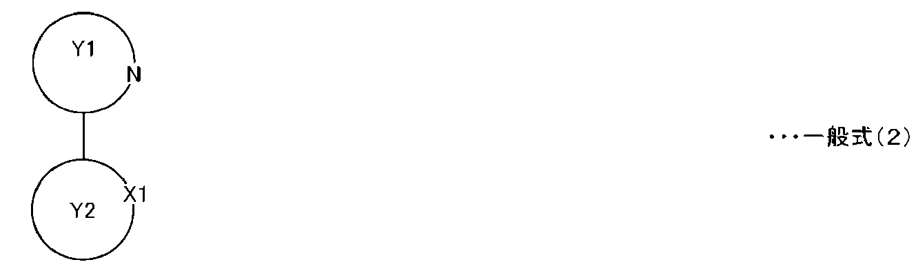
Y1で表わされる芳香族ヘテロ環としては、キノリン環、イソキノリン環、ピリジン環、キノキサリン環、チアゾール環、ピラゾール環、ピリミジン環、ベンゾチアゾール環、オキサゾール環、ベンゾオキサゾール環、インドール環、イソインドール環などがあげられる。Y2で表わされる芳香族炭化水素環または芳香族ヘテロ環としては、Y1にある芳香族ヘテロ環のほかに、ベンゼン環、ナフタレン環、アントラセン環、チオフェン環、ベンゾチオフェン環、フラン環、ベンゾフラン環、フルオレン環、ベンゾピラン環などがあげられる。前記芳香族ヘテロ環や芳香族炭化水素環に機能性基以外の置換基が付加されても構わない。置換基はたとえば、アルキル基(メチル基、エチル基)、置換アルキル基(トリフルオロメチル基)、アルコキシ基(メトキシ基)、ハロゲン原子(フッ素、塩素)、アミノ基、フェニル基などである。
Examples of the aromatic heterocycle represented by Y1 include quinoline ring, isoquinoline ring, pyridine ring, quinoxaline ring, thiazole ring, pyrazole ring, pyrimidine ring, benzothiazole ring, oxazole ring, benzoxazole ring, indole ring, isoindole ring, etc. Can be given. As the aromatic hydrocarbon ring or aromatic heterocycle represented by Y2, in addition to the aromatic heterocycle in Y1, benzene ring, naphthalene ring, anthracene ring, thiophene ring, benzothiophene ring, furan ring, benzofuran ring, Examples thereof include a fluorene ring and a benzopyran ring. Substituents other than functional groups may be added to the aromatic heterocycle or aromatic hydrocarbon ring. Examples of the substituent include an alkyl group (methyl group, ethyl group), a substituted alkyl group (trifluoromethyl group), an alkoxy group (methoxy group), a halogen atom (fluorine, chlorine), an amino group, and a phenyl group.
一般式(1)におけるL2はL1に含まれるものでもよいが、そのほかにアセチルアセトナート誘導体、ピコリネート誘導体、テトラキスピラゾリルボレート誘導体があげられる。
L2 in the general formula (1) may be contained in L1, but other examples include acetylacetonate derivatives, picolinate derivatives, and tetrakispyrazolyl borate derivatives.
青色ドーパントの固形分の濃度は10wt%以上30wt%以下が望ましく、緑色ドーパントの固形分の濃度は10wt%未満が望ましく、また、赤色ドーパントの固形分の濃度は10wt%未満が望ましい。発光ドーパントの重量平均分子量は500以上3000以下が望ましい。
The solid concentration of the blue dopant is desirably 10 wt% or more and 30 wt% or less, the solid content of the green dopant is desirably less than 10 wt%, and the solid content of the red dopant is desirably less than 10 wt%. The weight average molecular weight of the luminescent dopant is preferably 500 or more and 3000 or less.
<機能性基>
発光ドーパントの分子には、平面状、棒状、正四面体状、正八面体状、球状など様々な形状の分子が存在する。これらの分子に適切な機能性基を付加することで、基板面に対し略垂直に配向させることができる。分子を配向させることによって、遷移双極子モーメントの配向を制御する。 <Functional group>
The luminescent dopant molecule has various shapes such as a planar shape, a rod shape, a regular tetrahedral shape, a regular octahedral shape, and a spherical shape. By adding an appropriate functional group to these molecules, it can be oriented substantially perpendicular to the substrate surface. By orienting the molecules, the orientation of the transition dipole moment is controlled.
「略垂直に配向」とは、分子の平均値の基板面に対する垂直方向成分が、水平方向成分より大きくなることをいう。このとき、例えば平面状分子に注目した場合、平面状分子の平均値の基板面に対する垂直方向成分が、水平方向成分より大きくなっている。また、棒状分子に注目した場合、棒状分子の長軸の平均値の基板面に対する垂直方向成分が、水平方向成分より大きくなっている。なお、平面状分子とは例えば前記した縮合多環芳香族化合物や、一般式(1)で示される4配位金属錯体、また棒状分子とは短辺長と長辺長とのアスペクト比(短辺/長辺)が0.05~0.3の範囲にあるものをいう。
“Oriented substantially vertically” means that the vertical component of the average value of molecules with respect to the substrate surface is larger than the horizontal component. At this time, for example, when attention is paid to planar molecules, the vertical component of the average value of the planar molecules with respect to the substrate surface is larger than the horizontal component. When attention is paid to rod-like molecules, the vertical component of the average value of the long axes of the rod-like molecules with respect to the substrate surface is larger than the horizontal component. The planar molecule is, for example, the above-mentioned condensed polycyclic aromatic compound, the tetracoordinate metal complex represented by the general formula (1), or the rod-like molecule is an aspect ratio (short side length to short side length). (Side / long side) is in the range of 0.05 to 0.3.
発光ドーパントである平面分子または棒状分子に適切な機能性基を付加することで、基板面に対し略垂直に配向させることができる。
By adding an appropriate functional group to a planar molecule or rod-like molecule that is a luminescent dopant, it can be oriented substantially perpendicular to the substrate surface.
一般式(1)で示される金属錯体においては、2座配位子L1、L2のいずれか一方または両方に機能性基を付加する。機能性基としては表面エネルギーが小さいものもしくは下地層との相互作用が大きいものが好ましい。表面エネルギーが小さい機能性基を用いた場合には、成膜中に機能性基としては表面エネルギーが小さいフルオロアルキル基、パーフルオロアルキル基、アルキル基(ただしCの数が10以上)、パーフルオロポリエーテル基、シロキシ基(-Si-O-Si-)が挙げられる。表面エネルギーを考慮すれば、フルオロアルキル基、パーフルオロポリエーテル基が望ましく、パーフルオロアルキル基がさらに望ましい。フッ素を有する置換基では、フッ素の数が多いほど膜表面へと移動する作用が強い。具体的には、置換基に存在するフッ素の数が7以上であることが望ましい。これらの基は(化3)のように主骨格に直接導入してもよいが、結合角を考慮すると(化4)のようにアミド結合やエステル結合などを介して導入した方がより好ましい。
In the metal complex represented by the general formula (1), a functional group is added to one or both of the bidentate ligands L1 and L2. As the functional group, those having a small surface energy or those having a large interaction with the underlayer are preferable. When a functional group having a low surface energy is used, a functional group having a low surface energy is a fluoroalkyl group, a perfluoroalkyl group, an alkyl group (however, the number of C is 10 or more), perfluoro, and the like. Examples thereof include a polyether group and a siloxy group (—Si—O—Si—). Considering the surface energy, a fluoroalkyl group and a perfluoropolyether group are desirable, and a perfluoroalkyl group is more desirable. In the substituent having fluorine, the larger the number of fluorine, the stronger the action of moving to the film surface. Specifically, the number of fluorines present in the substituent is desirably 7 or more. These groups may be directly introduced into the main skeleton as in (Chemical Formula 3), but in consideration of the bond angle, it is more preferable to introduce them through an amide bond or an ester bond as in (Chemical Formula 4).
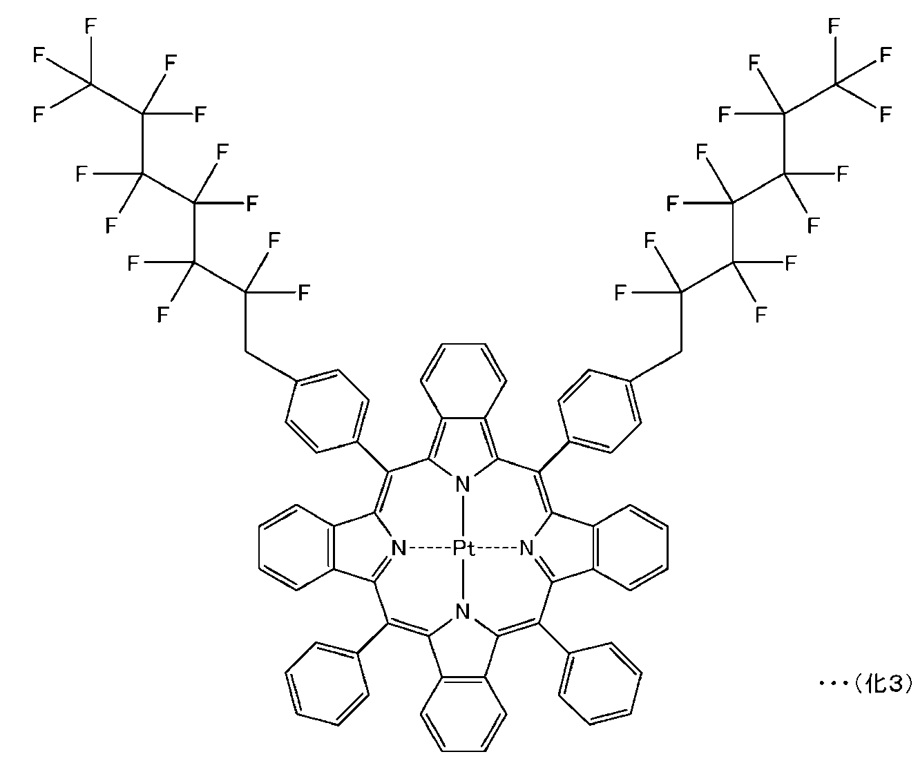

また下地層との相互作用が大きい機能性基としてはフェニルアミノ基、オキサゾール基、カルバゾール基、ヒドラゾン部位といった下地層(例えば正孔輸送層や電子輸送層など)と類似の構造であるものや、ヒドロキシ基(-OH)、チオール基(-SH)、カルボキシル基(-COOH)、スルホ基(-SO3H)、I、Br、Cl、F、SCN、CN、NH2、NO2、ビピリジル基があげられる。これらの基は、(化5)のように主骨格に直接導入してもよいが、分子の大きさや結合角を考慮し、アルキル鎖などを介して導入したほうが好ましい。
In addition, as a functional group having a large interaction with the underlayer, a functional group having a similar structure to an underlayer (such as a hole transport layer or an electron transport layer) such as a phenylamino group, an oxazole group, a carbazole group, or a hydrazone site, Hydroxy group (—OH), thiol group (—SH), carboxyl group (—COOH), sulfo group (—SO 3 H), I, Br, Cl, F, SCN, CN, NH 2 , NO 2 , bipyridyl group Can be given. These groups may be directly introduced into the main skeleton as in (Chemical Formula 5), but are preferably introduced via an alkyl chain in consideration of the size and bond angle of the molecule.

上記機能性基はドーパントに1つ以上付加する必要がある。機能性基は棒状分子の場合には分子の片末端に付加する。平面分子の場合には例えば、(化6)のように一方の配位子にのみ機能性基を付加する。より垂直に配向させるために棒状分子では片方の末端に表面エネルギーが低い機能性基を付加し、もう一方の末端に下地層と相互作用の強い機能性基を付加することが好ましい。また平面分子では、(化7)のように一方の配位子に表面エネルギーの低い機能性基を付加し、もう一方の配位子に下地層と相互作用の強い機能性基を付加することが好ましい。
It is necessary to add one or more functional groups to the dopant. In the case of a rod-like molecule, the functional group is added to one end of the molecule. In the case of a planar molecule, for example, a functional group is added to only one ligand as shown in (Chemical Formula 6). In order to align more vertically, it is preferable that a functional group having a low surface energy is added to one end of the rod-like molecule and a functional group having a strong interaction with the underlayer is added to the other end. For planar molecules, add a functional group with low surface energy to one ligand as shown in (Chemical Formula 7), and add a functional group that strongly interacts with the underlying layer to the other ligand. Is preferred.


<配向制御原理>
物質の表面は一般に内部(バルク)と異なり片側に同種の分子が存在しないため引力が働かずエネルギーが高く不安定である。そのため、表面エネルギーを低下させるために表面積を小さくするように変形させる力(表面張力)が働く。また、物質内に表面エネルギーの低い官能基を有する分子がある場合には、その官能基を表面に出すことで表面エネルギーを低下させ、安定化する。例えば、水と界面活性剤(両親媒性分子)の場合、界面活性剤は表面エネルギーの低い官能基である疎水基を分子内に有し、その疎水基を水面から出す形で水面に単分子膜を形成することで水面の表面エネルギー低下させている。 <Orientation control principle>
Unlike the inside (bulk), the surface of a substance is generally unstable because of the absence of the same kind of molecules on one side and no attractive force. Therefore, a force (surface tension) for deforming the surface area to reduce the surface energy acts. In addition, when there is a molecule having a functional group with low surface energy in the substance, the surface energy is lowered and stabilized by exposing the functional group to the surface. For example, in the case of water and a surfactant (amphiphilic molecule), the surfactant has a hydrophobic group, which is a functional group having a low surface energy, in the molecule, and the single molecule on the surface of the water in the form of releasing the hydrophobic group from the water surface. The surface energy of the water surface is reduced by forming a film.
本発明の分子は分子内にフルオロアルキル基などの表面エネルギーが低い官能基を有している。ベンゼン環などの部位はそれよりも表面エネルギーが高い。膜が形成される際には、表面エネルギーを小さくするために、上記表面エネルギーの低い官能基を表面に出すように力が働く。(化4)のように機能性基を付加した分子ではこの作用により表面エネルギーの低い官能基を膜表面に移動させることで分子面を基板面に対しおおむね垂直に配向させることができる。
The molecule of the present invention has a functional group with low surface energy such as a fluoroalkyl group in the molecule. Sites such as the benzene ring have higher surface energy. When a film is formed, a force acts to bring out the functional group having a low surface energy on the surface in order to reduce the surface energy. In a molecule to which a functional group is added as in (Chemical Formula 4), the molecular surface can be oriented almost perpendicularly to the substrate surface by moving a functional group having a low surface energy to the film surface by this action.
また下地層と相互作用を利用する場合には、下地層と機能性基の間に働く、分子間力、水素結合、配位結合の作用により機能性基が下地層に引き寄せられる。(化5)のように機能性基を付加した場合にはこの作用により分子面を基板面に対しておおむね垂直に配向させることができる。
In the case of utilizing the interaction with the underlayer, the functional group is attracted to the underlayer by the action of intermolecular force, hydrogen bond, and coordinate bond acting between the underlayer and the functional group. When a functional group is added as in (Chemical Formula 5), the molecular plane can be oriented almost perpendicularly to the substrate surface by this action.
また、(化7)のように、表面エネルギーの低い機能性基と下地層と相互作用の強い基の両方を付加することでより垂直に配向させることができる。
Also, as shown in (Chemical Formula 7), it is possible to align more vertically by adding both a functional group having a low surface energy and a group having a strong interaction with the underlying layer.
配向状態は、入射角を変化させながらIRスペクトル、あるいはラマンスペクトルを測定することで調べることができる。
The orientation state can be examined by measuring the IR spectrum or the Raman spectrum while changing the incident angle.
有機分子の配向状態は、入射角を変化させながらIRスペクトル、あるいはラマンスペクトルを測定することで調べることができる。
The orientation state of the organic molecule can be examined by measuring the IR spectrum or the Raman spectrum while changing the incident angle.
また遷移双極子モーメントの方向は、公知の方法で評価することができる。例えば(APPLIED PHYSICS LETTERS 96,073302(2010).)、フォトルミネッセンスのP偏光成分の放射角度依存性を、有機発光装置に光学接触させた半球レンズ・シリンドリカルレンズを用いて、薄膜デバイスの干渉効果を除いた上で、実験的に測定し、計算機シミュレーションと比較することで、遷移双極子モーメントにおける水平方向成分と垂直方向成分の各々の割合を求めることができる。これはP偏光強度の角度依存性が水平成分と垂直成分の割合により決まることによる(S偏光は水平成分のみから成る)。通常の発光層を構成する有機分子の配向はランダム(等方的)であり、そのため、遷移双極子モーメントの構成成分の割合は水平成分・垂直成分共に50%である。
Also, the direction of the transition dipole moment can be evaluated by a known method. For example (APPLIED PHYSICS LETTERS 96,073302 (2010).), Using the hemispherical lens / cylindrical lens optically contacting the organic light-emitting device to determine the radiation angle dependence of the P-polarized component of photoluminescence Then, the ratio of each of the horizontal component and the vertical component in the transition dipole moment can be obtained by experimental measurement and comparison with computer simulation. This is because the angle dependence of the P-polarized light intensity is determined by the ratio between the horizontal component and the vertical component (S-polarized light consists of only the horizontal component). The orientation of the organic molecules constituting the normal light emitting layer is random (isotropic), and therefore the proportion of the constituent components of the transition dipole moment is 50% for both the horizontal component and the vertical component.
<ホスト>
ホストとして、カルバゾール誘導体、フルオレン誘導体またはアリールシラン誘導体などを用いることが好ましい。効率の良い発光を得るためには青色ドーパントの励起エネルギーよりも、ホストの励起エネルギーが十分大きいことが好ましい。なお、励起エネルギーは発光スペクトルを用いて測定される。 <Host>
As the host, it is preferable to use a carbazole derivative, a fluorene derivative, an arylsilane derivative, or the like. In order to obtain efficient light emission, it is preferable that the excitation energy of the host is sufficiently larger than the excitation energy of the blue dopant. The excitation energy is measured using an emission spectrum.
<正孔注入層>
正孔注入層301とは発光効率や寿命を改善する目的で使用される。また、特に必須ではないが、陽極の凹凸を緩和する目的で使用される。正孔注入層301を単層もしくは複数層設けてもよい。正孔注入層301としては、PEDOT(ポリ(3、4-エチレンジオキシチオフェン)):PSS(ポリスチレンスルホネート)等の導電性高分子が好ましい。その他にも、ポリピロール系やトリフェニルアミン系のポリマー材料を用いることができる。また、低分子(重量平均分子量10000以下)材料系と組み合わせてよく用いられる、フタロシアニン類化合物やスターバーストアミン系化合物も適用可能である。 <Hole injection layer>
Thehole injection layer 301 is used for the purpose of improving luminous efficiency and lifetime. Moreover, although it is not essential, it is used for the purpose of relaxing the unevenness of the anode. The hole injection layer 301 may be provided as a single layer or a plurality of layers. The hole injection layer 301 is preferably a conductive polymer such as PEDOT (poly (3,4-ethylenedioxythiophene)): PSS (polystyrene sulfonate). In addition, polypyrrole-based or triphenylamine-based polymer materials can be used. Further, phthalocyanine compounds and starburst amine compounds that are often used in combination with a low molecular weight (weight average molecular weight 10,000 or less) material system are also applicable.
正孔注入層301とは発光効率や寿命を改善する目的で使用される。また、特に必須ではないが、陽極の凹凸を緩和する目的で使用される。正孔注入層301を単層もしくは複数層設けてもよい。正孔注入層301としては、PEDOT(ポリ(3、4-エチレンジオキシチオフェン)):PSS(ポリスチレンスルホネート)等の導電性高分子が好ましい。その他にも、ポリピロール系やトリフェニルアミン系のポリマー材料を用いることができる。また、低分子(重量平均分子量10000以下)材料系と組み合わせてよく用いられる、フタロシアニン類化合物やスターバーストアミン系化合物も適用可能である。 <Hole injection layer>
The
<正孔輸送層>
正孔輸送層302とは正孔を輸送する機能を有する材料からなり、広い意味で正孔注入層301、電子阻止層も正孔輸送層に含まれる。正孔輸送層302を単層もしくは複数層設けてもよい。正孔輸送層302としては、スターバーストアミン系化合物やスチルベン誘導体、ヒドラゾン誘導体、チオフェン誘導体などを用いることができる。また、これらの材料に限られるものではなく、これらの材料を2種以上併用しても差し支えない。 <Hole transport layer>
Thehole transport layer 302 is made of a material having a function of transporting holes. In a broad sense, the hole injection layer 301 and the electron blocking layer are also included in the hole transport layer. The hole transport layer 302 may be provided as a single layer or a plurality of layers. As the hole-transport layer 302, a starburst amine compound, a stilbene derivative, a hydrazone derivative, a thiophene derivative, or the like can be used. Further, the present invention is not limited to these materials, and two or more of these materials may be used in combination.
正孔輸送層302とは正孔を輸送する機能を有する材料からなり、広い意味で正孔注入層301、電子阻止層も正孔輸送層に含まれる。正孔輸送層302を単層もしくは複数層設けてもよい。正孔輸送層302としては、スターバーストアミン系化合物やスチルベン誘導体、ヒドラゾン誘導体、チオフェン誘導体などを用いることができる。また、これらの材料に限られるものではなく、これらの材料を2種以上併用しても差し支えない。 <Hole transport layer>
The
<電子輸送層>
電子輸送層304は発光層303に電子を供給する層である。広い意味で電子注入層305、正孔阻止層も電子輸送層304に含まれる。電子輸送層304を単層もしくは複数層設けてもよい。この電子輸送層304の材料としては、例えば、ビス(2-メチル-8-キノリノラト)-4-(フェニルフェノラト)アルミニウム(以下、BAlq)や、トリス(8-キノリノラト)アルミニウム(以下、Alq3)、Tris(2、4、6-trimethyl-3-(pyridin-3-yl)phenyl)borane(以下、3TPYMB)、1、4-Bis(triphenylsilyl)benzene(以下、UGH2)、オキサジアゾール誘導体、トリアゾール誘導体、フラーレン誘導体、フェナントロリン誘導体、キノリン誘導体などを用いることができる。 <Electron transport layer>
Theelectron transport layer 304 is a layer that supplies electrons to the light emitting layer 303. In a broad sense, the electron injection layer 305 and the hole blocking layer are also included in the electron transport layer 304. The electron transport layer 304 may be provided as a single layer or a plurality of layers. Examples of the material for the electron transport layer 304 include bis (2-methyl-8-quinolinolato) -4- (phenylphenolato) aluminum (hereinafter referred to as BAlq) and tris (8-quinolinolato) aluminum (hereinafter referred to as Alq3). , Tris (2,4,6-trimethyl-3- (pyridin-3-yl) phenyl) borane (hereinafter 3TPYMB), 1,4-Bis (triphenylsilyl) benzene (hereinafter UGH2), oxadiazole derivative, triazole Derivatives, fullerene derivatives, phenanthroline derivatives, quinoline derivatives, and the like can be used.
電子輸送層304は発光層303に電子を供給する層である。広い意味で電子注入層305、正孔阻止層も電子輸送層304に含まれる。電子輸送層304を単層もしくは複数層設けてもよい。この電子輸送層304の材料としては、例えば、ビス(2-メチル-8-キノリノラト)-4-(フェニルフェノラト)アルミニウム(以下、BAlq)や、トリス(8-キノリノラト)アルミニウム(以下、Alq3)、Tris(2、4、6-trimethyl-3-(pyridin-3-yl)phenyl)borane(以下、3TPYMB)、1、4-Bis(triphenylsilyl)benzene(以下、UGH2)、オキサジアゾール誘導体、トリアゾール誘導体、フラーレン誘導体、フェナントロリン誘導体、キノリン誘導体などを用いることができる。 <Electron transport layer>
The
<電子注入層>
電子注入層305は陰極から電子輸送層304への電子注入効率を向上させる。具体的には、弗化リチウム、弗化マグネシウム、弗化カルシウム、弗化ストロンチウム、弗化バリウム、酸化マグネシウム、酸化アルミニウムが望ましい。また、もちろんこれらの材料に限られるわけではなく、また、これらの材料を2種以上併用しても差し支えない。 <Electron injection layer>
Theelectron injection layer 305 improves the electron injection efficiency from the cathode to the electron transport layer 304. Specifically, lithium fluoride, magnesium fluoride, calcium fluoride, strontium fluoride, barium fluoride, magnesium oxide, and aluminum oxide are desirable. Of course, the material is not limited to these materials, and two or more of these materials may be used in combination.
電子注入層305は陰極から電子輸送層304への電子注入効率を向上させる。具体的には、弗化リチウム、弗化マグネシウム、弗化カルシウム、弗化ストロンチウム、弗化バリウム、酸化マグネシウム、酸化アルミニウムが望ましい。また、もちろんこれらの材料に限られるわけではなく、また、これらの材料を2種以上併用しても差し支えない。 <Electron injection layer>
The
<基板>
基板100として、ガラス基板、金属基板、SiO2、SiNx、Al2O3等の無機材料を形成したプラスチック基板等が挙げられる。金属基板材料としては、ステンレス、42アロイなどの合金が挙げられる。プラスチック基板材料としては、ポリエチレンテレフタレート、ポリエチレンナフタレート、ポリメチルメタクリレート、ポリサルフォン、ポリカーボネート、ポリイミド等が挙げられる。 <Board>
Examples of thesubstrate 100 include a glass substrate, a metal substrate, a plastic substrate on which an inorganic material such as SiO 2 , SiNx, and Al 2 O 3 is formed. Examples of the metal substrate material include alloys such as stainless steel and 42 alloy. Examples of the plastic substrate material include polyethylene terephthalate, polyethylene naphthalate, polymethyl methacrylate, polysulfone, polycarbonate, and polyimide.
基板100として、ガラス基板、金属基板、SiO2、SiNx、Al2O3等の無機材料を形成したプラスチック基板等が挙げられる。金属基板材料としては、ステンレス、42アロイなどの合金が挙げられる。プラスチック基板材料としては、ポリエチレンテレフタレート、ポリエチレンナフタレート、ポリメチルメタクリレート、ポリサルフォン、ポリカーボネート、ポリイミド等が挙げられる。 <Board>
Examples of the
<陽極>
陽極材料としては、透明性と高い仕事関数を有する材料であれば用いることができる。具体的には、ITO、IZOなどの導電性酸化物や、薄いAgなどの仕事関数の大きい金属が挙げられる。電極のパターン形成は、一般的にはガラス等の基板上にホトリソグラフィーなどを用いて行うことができる。 <Anode>
As the anode material, any material having transparency and a high work function can be used. Specifically, conductive oxides such as ITO and IZO and metals having a large work function such as thin Ag can be used. In general, the electrode pattern can be formed on a substrate such as glass by using photolithography.
<プラズモン取出しナノ構造を含む陰極>
また陰極は、表面プラズモンポラリトンを誘起・散乱できる凹凸構造を有することが必要である。凹凸の最大の高さ、幅及びピッチは発光波長より小さい大きさであればよいため、5nm以上、800nm以下が望ましい。発光波長は可視光であるため、380nmから800nmの範囲である。また凹凸のサイズが10nmより小さいと作成が困難となる、高コスト化する、可視領域より短波長側を増幅する、等の問題が出てくる。また800nmよりも大きいと可視光を散乱し難くなる。このような膜を本明細書ではプラズモン取出しナノ構造と称す。具体的には、表面が粒状の粒状膜、或いは金属微粒子を膜状に非周期的に或いは周期的な配列パターン状に分散させ、微粒子間に空隙が存在する島状構造膜が好適である。陰極が島状構造膜であることにより、発光光により陰極に誘起された表面プラズモンポラリトンが、再度、可視光に変換され、内部量子効率及び発光効率が向上する。 <Cathode including plasmon extraction nanostructure>
Further, the cathode needs to have an uneven structure capable of inducing and scattering surface plasmon polaritons. Since the maximum height, width, and pitch of the unevenness may be smaller than the emission wavelength, 5 nm or more and 800 nm or less are desirable. Since the emission wavelength is visible light, it is in the range of 380 nm to 800 nm. In addition, when the size of the unevenness is smaller than 10 nm, it becomes difficult to produce, the cost is increased, and the wavelength shorter than the visible region is amplified. If it is larger than 800 nm, it becomes difficult to scatter visible light. Such a film is referred to herein as a plasmon extraction nanostructure. Specifically, a granular film having a granular surface or an island-shaped structure film in which metal fine particles are dispersed non-periodically or in a periodic arrangement pattern in a film shape and voids exist between the fine particles is preferable. Since the cathode is an island-shaped structure film, the surface plasmon polariton induced in the cathode by the emitted light is converted again to visible light, and the internal quantum efficiency and the luminous efficiency are improved.
陰極材料としては、Al、Ag、Au、Cu並びにLiFとAlの積層体やMg:Ag合金等が好適に用いられる。また、これらの材料に限定されるものではなく、例えばLiFの代わりとして、Cs化合物、Ba化合物、Ca化合物などを用いることができる。またプラズモン取出しナノ構造の高さは、励起有機分子の作る近接場と表面プラズモンポラリトン共鳴が強く生じるようにするために、40nmから120nmであることが望ましい。材料面では、特に励起有機分子の作る近接場と表面プラズモンポラリトン共鳴が強く生じるものであればより望ましく、Ag、Au、Cu及びAlの金属のいずれかを主成分(80%以上)とする合金が適用可能である。なお、特に、発光光が可視域波長であれば、Agが望ましい。プラズマ周波数から、Agは可視域での表面プラズモン共鳴が起こせるためである。発光光が可視域以外の波長、たとえば赤外であれば、Auが望ましい。
As the cathode material, Al, Ag, Au, Cu, a laminate of LiF and Al, an Mg: Ag alloy, or the like is preferably used. Moreover, it is not limited to these materials, For example, a Cs compound, Ba compound, Ca compound etc. can be used instead of LiF. The height of the plasmon extraction nanostructure is preferably 40 nm to 120 nm so that the near field formed by the excited organic molecule and the surface plasmon polariton resonance are strongly generated. In terms of materials, it is more desirable that the near-field generated by the excited organic molecule and the surface plasmon polariton resonance are strong, and an alloy containing any one of Ag, Au, Cu and Al as a main component (80% or more). Is applicable. In particular, Ag is desirable when the emitted light is a visible wavelength. This is because Ag can cause surface plasmon resonance in the visible range from the plasma frequency. If the emitted light has a wavelength other than the visible range, for example, infrared, Au is desirable.
なお、上述のような有機発光素子は、例えば、基板上に陰極側から順次積層されて、陽極側から光が取り出させるように構成される。陰極は、例えば、スパッタ法、真空蒸着法などを用いて形成することができる。又プラズモン取出しナノ構造は公知のホトリソグラフィーやロールを用いたエンボス加工等を陰極に施すことにより作成することができる。また下地基板に又プラズモン取出しナノ構造と同程度のサイズの凹凸を形成し、その上に、発光層等を形成することにより、下地の凹凸を上層に反映させる形でプラズモン取出しナノ構造を形成してもよい。また、プラズモン取出しができるようなサイズの金属ナノ粒子を平坦な金属電極の上に塗布して形成してもよい。また、SAM(自己組織化単分子膜)を用いて、金奥ナノ粒子を金属電極上に固定化してもよい。また、金属電極薄膜を蒸着した後、大気圧或いは還元雰囲気中で加熱する方法や、金属電極薄膜を蒸着する際に不均一な島状構造が自発的に形成する現象を用いてもよい。また基板にポリスチレンなどの直径100nm程度のナノスフィアを塗布・堆積させ、その上に金属を蒸着することで、ナノスフィア上部に帽子状に金属薄膜が堆積した構造を作製してもよい。
Note that the organic light emitting element as described above is configured, for example, so that it is sequentially stacked on the substrate from the cathode side, and light is extracted from the anode side. The cathode can be formed using, for example, a sputtering method, a vacuum evaporation method, or the like. The plasmon extraction nanostructure can be prepared by subjecting the cathode to known photolithography or embossing using a roll. In addition, by forming irregularities of the same size as the plasmon extraction nanostructure on the base substrate, and forming a light emitting layer etc. on it, the plasmon extraction nanostructure is formed in a form that reflects the irregularities of the underlying layer on the upper layer. May be. Alternatively, metal nanoparticles having such a size that plasmon can be extracted may be applied on a flat metal electrode. Alternatively, the gold back nanoparticles may be immobilized on the metal electrode using SAM (self-assembled monolayer). Moreover, after vapor-depositing a metal electrode thin film, a method of heating in an atmospheric pressure or a reducing atmosphere, or a phenomenon in which a non-uniform island structure is spontaneously formed when the metal electrode thin film is vapor-deposited may be used. Alternatively, a nanosphere having a diameter of about 100 nm, such as polystyrene, may be applied to and deposited on a substrate, and a metal may be vapor-deposited on the nanosphere to produce a structure in which a metal thin film is deposited on the top of the nanosphere.
なお、表面プラズモンポラリトンの励起及び可視光の散乱の寿命は一般的に通常の発光再結合速度及び非発光再結合速度よりも早いことが多く、従って、発光寿命を測定することにより、表面プラズモンポラリトンを介した発光であることの確認ができる。
It should be noted that the lifetime of surface plasmon polariton excitation and visible light scattering is generally faster than the normal luminescence and non-radiative recombination rates, and therefore, by measuring the luminescence lifetime, surface plasmon polariton can be obtained. It can be confirmed that the light is emitted through the.
<上部電極と下部電極並びに透明電極と反射電極の関係>
有機発光素子には基板/透明電極(陽極)/有機層/反射電極(陰極)として有機層からの発光を基板側(透明電極のある側)から取り出すボトムエミッション型と、基板/反射電極(陰極)/有機層/透明電極(陽極)として有機層からの発光を基板とは反対の側(透明電極のある側)から取り出すトップエミッション型とがある。ボトムエミッション型の場合、透明電極(陽極)が下部電極、反射電極(陰極)が上部電極となる。またトップエミッション型の場合、反射電極(陰極)が下部電極、透明電極(陽極)が上部電極となる。本発明ではボトムエミッション型のとき、上部電極にプラズモン取出しナノ構造を設けることが重要である。またトップエミッション型のとき、下部電極にプラズモン取出しナノ構造を設けることが重要である。どちらの型の場合も反射電極の発光層側の表面にプラズモン取出しナノ構造を設けることが重要である。 <Relationship between upper electrode and lower electrode, and transparent electrode and reflective electrode>
The organic light emitting device includes a bottom emission type in which light from the organic layer is extracted from the substrate side (side with the transparent electrode) as a substrate / transparent electrode (anode) / organic layer / reflecting electrode (cathode), and a substrate / reflecting electrode (cathode). ) / Organic layer / transparent electrode (anode) is a top emission type in which light emitted from the organic layer is extracted from the side opposite to the substrate (the side with the transparent electrode). In the case of the bottom emission type, the transparent electrode (anode) is the lower electrode, and the reflective electrode (cathode) is the upper electrode. In the case of the top emission type, the reflective electrode (cathode) is the lower electrode and the transparent electrode (anode) is the upper electrode. In the present invention, in the bottom emission type, it is important to provide a plasmon extraction nanostructure on the upper electrode. In the case of the top emission type, it is important to provide a plasmon extraction nanostructure on the lower electrode. In either case, it is important to provide a plasmon extraction nanostructure on the surface of the reflective electrode on the light emitting layer side.
<塗液>
塗液は発光層303を形成する材料を適切な溶媒に溶解させたものである。以下の説明では、発光層303を形成する材料としてホスト、赤色ドーパント、緑色ドーパント及び青色ドーパントが含まれえる場合について述べる。 <Coating liquid>
The coating liquid is obtained by dissolving the material forming thelight emitting layer 303 in an appropriate solvent. In the following description, a case where a host, a red dopant, a green dopant, and a blue dopant can be included as a material for forming the light emitting layer 303 will be described.
塗液は発光層303を形成する材料を適切な溶媒に溶解させたものである。以下の説明では、発光層303を形成する材料としてホスト、赤色ドーパント、緑色ドーパント及び青色ドーパントが含まれえる場合について述べる。 <Coating liquid>
The coating liquid is obtained by dissolving the material forming the
ここで用いる溶媒は、例えばトルエンなど芳香族炭化水素系溶媒、テトラヒドロフランなどのエーテル系溶媒、アルコール類、フッ素系溶媒など各材料が溶解するものであればよい。また、各材料の溶解度や、乾燥速度の調整のために前述の溶媒を複数混合した混合溶媒でもかまわない。例えば、沸点の異なる溶媒を2種類(第一の溶媒及び第二の溶媒)用意し、そのうち高沸点である第二の溶媒を緑色または青色ドーパントに対し溶媒とすることで緑色ドーパントまたは青色ドーパントの膜表面への移動を促進できる。溶媒の溶解度は液体クロマトグラム法によって測定される。
The solvent used here may be any solvent that can dissolve each material such as an aromatic hydrocarbon solvent such as toluene, an ether solvent such as tetrahydrofuran, alcohols, and a fluorine solvent. Further, a mixed solvent in which a plurality of the above-mentioned solvents are mixed for adjusting the solubility of each material and the drying speed may be used. For example, two types of solvents having different boiling points (first solvent and second solvent) are prepared, and the second solvent having a high boiling point is used as a solvent for the green or blue dopant. The movement to the film surface can be promoted. The solubility of the solvent is measured by a liquid chromatogram method.
発光層303を成膜法としては乾式法では真空蒸着法など、湿式法(塗布法)としては、スピンコート法、キャスト法、ディップコート法、スプレーコート法、スクリーン印刷法、インクジェット印刷法、スロットダイコート法、グラビアコート法、バーコート法などを挙げることができる。これらの方法のうち1つを用いて、発光層303を形成する。
The light emitting layer 303 is formed by a dry method such as a vacuum deposition method, and as a wet method (coating method), a spin coating method, a casting method, a dip coating method, a spray coating method, a screen printing method, an ink jet printing method, a slot Examples thereof include a die coating method, a gravure coating method, and a bar coating method. The light emitting layer 303 is formed using one of these methods.
塗布法は乾式法に比べて大面積の成膜が容易、材料の利用効率が高いなどの利点がある。
次に、本発明の具体的な実施例を説明する。本発明が以下の実施例に限定されるものでないことは先述の通りである。 Compared with the dry method, the coating method has advantages such as easy formation of a large area and high material utilization efficiency.
Next, specific examples of the present invention will be described. As described above, the present invention is not limited to the following examples.
本発明の第1の実施例として図4に示す構造の白色発光素子を作製した。
As a first example of the present invention, a white light emitting device having the structure shown in FIG. 4 was produced.
基板100は以下のように作製した。石英基板上にフォトレジスト(東京応化製:THMR-iP3300)を塗布し、He-Cdレーザー(波長:325nm)による2光子干渉縞を60°角度を変えて2重露光の後、現像し、反応性イオンエッチングにより基板をエッチングした、その後にフォトレジストを除去し、基板上に凹凸を形成した。このときの凹凸の深さは70nm、凹凸のピッチは420nmであった。この基板の上に、下記の通り成膜を行うことによって、基板の凹凸を保ったまま、有機発光素子が形成でき、最終的に蒸着したAl膜も下地の凹凸を反映した、プラズモン取出しナノ構造を作製できる。
The substrate 100 was produced as follows. Photoresist (manufactured by Tokyo Ohka: THMR-iP3300) is coated on a quartz substrate, and two-photon interference fringes by He-Cd laser (wavelength: 325 nm) are changed by 60 ° angle, developed after double exposure, and reacted. The substrate was etched by reactive ion etching, and then the photoresist was removed to form irregularities on the substrate. At this time, the depth of the unevenness was 70 nm, and the pitch of the unevenness was 420 nm. By forming a film on this substrate as described below, an organic light-emitting device can be formed while maintaining the unevenness of the substrate, and the finally deposited Al film also reflects the unevenness of the underlying plasmon extraction nanostructure Can be produced.
下部電極(透明電極)としてITO電極をスパッタで形成した。正孔注入層301にはPEDOTをスピンコート法にて形成した。正孔輸送層302にはポリマー系の材料を用いた。発光層303はホストとしてmCP(1、3-ビス(カルバゾル-9-イル)ベンゼン)、青色ドーパントには(化7)、赤色ドーパントには(化3)、緑色ドーパントには(化6)を用いた。青色ドーパントの発光波長は460nmである。それぞれの材料の重量比は100:10:0.5:0.5とした。これらのホスト、青色、赤色、緑色ドーパントをトルエンに溶解させて塗液を作製した。塗液の固形成分濃度は1wt%に設定した。この塗液を用いて、スピンコート法により有機発光層を形成した。続いて電子輸送層304としてUGH2および3TPYMBの層を真空蒸着法で形成した。次にLiFとAlの積層体を上部電極(反射電極)として形成した。先述のように、上部電極(反射電極)は基板の凹凸を保持しているため、プラズモン取出しナノ構造が形成できている。このようにして、ボトムエミッション型の有機発光素子を作製した。発光位置は各色ドーパントとも上部電極(反射電極)から75nm近傍となるようにした。
An ITO electrode was formed by sputtering as a lower electrode (transparent electrode). PEDOT was formed on the hole injection layer 301 by spin coating. A polymer material was used for the hole transport layer 302. The light-emitting layer 303 includes mCP (1,3-bis (carbazol-9-yl) benzene) as a host, (Chemical formula 7) for a blue dopant, (Chemical formula 3) for a red dopant, and (Chemical formula 6) for a green dopant. Using. The emission wavelength of the blue dopant is 460 nm. The weight ratio of each material was 100: 10: 0.5: 0.5. These host, blue, red, and green dopants were dissolved in toluene to prepare a coating solution. The solid component concentration of the coating liquid was set to 1 wt%. Using this coating liquid, an organic light emitting layer was formed by spin coating. Subsequently, UGH2 and 3TPYMB layers were formed as the electron transport layer 304 by a vacuum deposition method. Next, a laminated body of LiF and Al was formed as an upper electrode (reflection electrode). As described above, since the upper electrode (reflective electrode) holds the unevenness of the substrate, a plasmon extraction nanostructure can be formed. In this way, a bottom emission type organic light emitting device was produced. The emission position of each color dopant was set to be around 75 nm from the upper electrode (reflection electrode).
作製した有機発光素子に電圧を印加したところ、3つのドーパントからの発光がELスペクトルから確認され、白色発光が確認できた。また、比較例1-1として機能性基を付加しないドーパントを用いた素子を作製し、比較例1-2として石英基板にプラズモン取出しナノ構造を作製していない素子を作製した。比較例1-2の構成を図5に示す。比較例1-1の発光効率を1とすると、実施例1は1.31倍高い発光効率を示し、又比較例1-2の発光効率は比較例1-1の0.15倍であった。
When a voltage was applied to the produced organic light emitting device, light emission from the three dopants was confirmed from the EL spectrum, and white light emission was confirmed. Further, as Comparative Example 1-1, an element using a dopant that does not add a functional group was produced, and as Comparative Example 1-2, an element in which a plasmon extraction nanostructure was not produced on a quartz substrate was produced. The configuration of Comparative Example 1-2 is shown in FIG. Assuming that the luminous efficiency of Comparative Example 1-1 is 1, Example 1 shows a luminous efficiency 1.31 times higher, and the luminous efficiency of Comparative Example 1-2 was 0.15 times that of Comparative Example 1-1. .
なお、実施例1と同様の構成の発光層を別途試作し、フォトルミネッセンス測定において、P偏光強度の角度依存性を測定し、各色ドーパントの遷移双極子モーメントの構成成分の割合を調べたところ、各色とも垂直成分が95%であった。他方で、比較例1-1においては各色とも水平成分が50%であった。比較例1-2は機能性基を付加したドーパントを用いているため、実施例1と同じく、各色とも垂直成分が95%であった。
In addition, when a light emitting layer having the same configuration as that of Example 1 was separately prototyped, and the photoluminescence measurement was performed to measure the angle dependency of the P-polarized light intensity, and the proportion of the constituent components of the transition dipole moment of each color dopant was examined, The vertical component of each color was 95%. On the other hand, in Comparative Example 1-1, the horizontal component of each color was 50%. Since Comparative Example 1-2 used a dopant with a functional group added, the vertical component of each color was 95% as in Example 1.
なお本明細書の前半部で説明したように、遷移双極子モーメントの方向が等方的である場合、励起子エネルギーの約75%が可視光に変換され、25%が表面プラズモンポラリトンに由来する損失となる。従って遷移双極子モーメントの方向が等方的である比較例1-1に対して、遷移双極子モーメントの方向が略垂直であり、かつプラズモン取出しナノ構造を有する実施例1の発光効率が1.31(<(25+75)/75≒1.33)倍であるということは、表面プラズモンポラリトンによる損失の大半が、プラズモン取出しナノ構造により可視光に変換されたためと考えられ、効率向上としては上限に近い十分大きな値である。他方で比較例2では大きく発光効率が低下した。これは機能性基により各色のドーパントの遷移双極子モーメントの方向が略垂直となったために、大半の励起子エネルギーが表面プラズモンポラリトンによる損失となったためと考えられる。
As described in the first half of this specification, when the direction of the transition dipole moment is isotropic, about 75% of the exciton energy is converted into visible light, and 25% is derived from the surface plasmon polariton. Loss. Therefore, in contrast to Comparative Example 1-1 in which the direction of the transition dipole moment is isotropic, the light emission efficiency of Example 1 in which the direction of the transition dipole moment is substantially perpendicular and has a plasmon extraction nanostructure is 1. 31 (<(25 + 75) /75≈1.33) times is considered that most of the loss due to the surface plasmon polariton was converted to visible light by the plasmon extraction nanostructure, and the upper limit for improving efficiency A close enough large value. On the other hand, in Comparative Example 2, the luminous efficiency was greatly reduced. This is presumably because most of the exciton energy was lost due to surface plasmon polaritons because the direction of the transition dipole moment of the dopants of each color became substantially vertical due to the functional group.
また発光寿命を以下のようにして測定した。窒素レーザー光(波長337nm、パルス幅1ns)を励起光として各素子に照射し、それぞれの発光材料からの発光寿命をストリークカメラ(浜松ホトニクス社製C4334)により測定した。その結果、実施例1の発光寿命が24nsだったのに対して、比較例1-1の発光寿命は30ns、比較例1-2の発光寿命は624nsであった。従って、実施例1及び比較例1-2では確かに表面プラズモンポラリトンを介した発光が観測されていると考えられる。また特に実施例1ではプラズモン取出しナノ構造による発光効率の向上効果が比較例1-2の場合よりも大きく得られている。
Moreover, the light emission lifetime was measured as follows. Nitrogen laser light (wavelength 337 nm, pulse width 1 ns) was irradiated to each element as excitation light, and the light emission lifetime from each light emitting material was measured with a streak camera (C4334 manufactured by Hamamatsu Photonics). As a result, the emission lifetime of Example 1 was 24 ns, whereas that of Comparative Example 1-1 was 30 ns, and that of Comparative Example 1-2 was 624 ns. Therefore, in Example 1 and Comparative Example 1-2, it is considered that light emission via surface plasmon polaritons is observed. In particular, in Example 1, the effect of improving the light emission efficiency by the plasmon extraction nanostructure is larger than that in Comparative Example 1-2.
本発明の第2の実施例として、複数の有機発光素子を接続した光源装置を作製した。作製した素子は、実施例1と同様の基板、層構成で、発光層にホストと赤色ドーパントとして(化3)、緑色ドーパントとして(化5)を含む素子(RG素子)と発光層にホストと青色ドーパントとして(化4)を含む素子(B素子)を面内に作りわけ、各素子を直列および並列に接続した。青色ドーパントの発光波長は450nmである。塗布膜の作製にはインクジェット法を用いた。発光位置は各色ドーパントとも上部電極(反射電極)から75nm近傍となるようにした。均質な白色光を得るために、作製した素子の発光面に拡散板を取り付けた。作製した光源装置では良好な白色光が得られた。また、比較例2として機能性基を付加しないドーパントを用いた素子を作製した。実施例2は比較例2と比較して1.18倍高い発光効率を示した。なお、実施例2と同様の構成の発光層を別途試作し、フォトルミネッセンス測定において、P偏光強度の角度依存性を測定し、各色ドーパントの遷移双極子モーメントの構成成分の割合を調べたところ、各色とも垂直成分が84%以上であった。他方で、比較例2においては各色とも垂直成分が約50%であった。
As a second example of the present invention, a light source device in which a plurality of organic light emitting elements were connected was produced. The fabricated device has the same substrate and layer structure as in Example 1, with the light-emitting layer containing a host and a red dopant (Chemical Formula 3), and a green dopant (Chemical Formula 5) and a light-emitting layer with a host. An element (B element) containing (chemical formula 4) as a blue dopant was formed in-plane, and each element was connected in series and in parallel. The emission wavelength of the blue dopant is 450 nm. An inkjet method was used for producing the coating film. The emission position of each color dopant was set to be around 75 nm from the upper electrode (reflection electrode). In order to obtain uniform white light, a diffusion plate was attached to the light emitting surface of the fabricated device. In the produced light source device, good white light was obtained. Moreover, the element using the dopant which does not add a functional group as the comparative example 2 was produced. Example 2 showed 1.18 times higher luminous efficiency than Comparative Example 2. In addition, when a light emitting layer having the same configuration as that of Example 2 was separately prototyped, in the photoluminescence measurement, the angle dependency of the P-polarized light intensity was measured, and the ratio of the constituent components of the transition dipole moment of each color dopant was examined. The vertical component of each color was 84% or more. On the other hand, in Comparative Example 2, the vertical component of each color was about 50%.
実施例1と同様に、発光効率が1.18倍であるということは、表面プラズモンポラリトンによる損失のかなりの割合が、プラズモン取出しナノ構造により可視光に変換されたためと考えられ、効率向上としては十分大きな値である。
As in Example 1, the luminous efficiency is 1.18 times because it is considered that a considerable proportion of the loss due to the surface plasmon polariton was converted to visible light by the plasmon extraction nanostructure. It is a sufficiently large value.
また拡散板をつけることにより、発光層において励起子エネルギーからプラズモン取出しナノ構造を介して発生した可視光の内の、より多くを外部(空気)へと取出すことができる。従って、遷移双極子モーメントの方向が略垂直であり、プラズモン取出しナノ構造を有することによる効率向上効果がさらに増幅され、より発光効率の高い光源装置を得ることができる。
Also, by attaching a diffuser plate, it is possible to extract more of the visible light generated from the exciton energy from the exciton energy in the light emitting layer through the nanostructure to the outside (air). Therefore, the direction of the transition dipole moment is substantially vertical, and the efficiency improvement effect by having the plasmon extraction nanostructure is further amplified, and a light source device with higher luminous efficiency can be obtained.
本発明の第三の実施例として、複数の有機発光素子を接続した光源装置を作製した。作製した素子は、実施例1と同様の基板、層構成で、発光層にホストと赤色ドーパントとして(化3)を含む素子(R素子)と、発光層にホスト材料と緑色ドーパントとして(化6)を含む素子(G素子)と発光層にホストと青色ドーパントとして(化4)を含む素子(B素子)を面内に作りわけ、各素子を直列および並列に接続した。青色ドーパントの発光波長は455nmである。塗布膜の作製にはインクジェット法を用いた。発光位置は各色ドーパントとも上部電極(反射電極)から75nm近傍となるようにした。均質な白色光を得るために、作製した素子の発光面に拡散板を取り付けた。作製した光源装置では良好な白色光が得られた。また、比較例3として機能性基を付加しないドーパントを用いた素子を作製した。実施例3は比較例3と比較して1.23倍高い発光効率を示した。なお、実施例3と同様の構成の発光層を別途試作し、フォトルミネッセンス測定において、P偏光強度の角度依存性を測定し、各色ドーパントの遷移双極子モーメントの構成成分の割合を調べたところ、各色とも垂直成分が90%以上であった。他方で、比較例2においては各色とも垂直成分が約50%であった。
As a third example of the present invention, a light source device in which a plurality of organic light emitting elements were connected was produced. The produced device has the same substrate and layer structure as in Example 1, the device containing the host and red dopant (Chemical Formula 3) in the light emitting layer (R device), and the host material and green dopant in the light emitting layer (Chemical formula 6). ) And a light emitting layer containing a host and a blue dopant (Chemical element 4) (B element) were formed in-plane, and the respective elements were connected in series and in parallel. The emission wavelength of the blue dopant is 455 nm. An inkjet method was used for producing the coating film. The emission position of each color dopant was set to be around 75 nm from the upper electrode (reflection electrode). In order to obtain uniform white light, a diffusion plate was attached to the light emitting surface of the fabricated device. In the produced light source device, good white light was obtained. Moreover, the element using the dopant which does not add a functional group as the comparative example 3 was produced. Example 3 showed a luminous efficiency 1.23 times higher than that of Comparative Example 3. In addition, when a light emitting layer having the same configuration as in Example 3 was separately prototyped, the photoluminescence measurement was performed to measure the angle dependence of the P-polarized light intensity, and the proportion of the constituent components of the transition dipole moment of each color dopant was examined. The vertical component of each color was 90% or more. On the other hand, in Comparative Example 2, the vertical component of each color was about 50%.
実施例1と同様に、発光効率が1.23倍であるということは、表面プラズモンポラリトンによる損失のかなりの割合がプラズモン取出しナノ構造により可視光に変換されたためと考えられ、効率向上としては十分大きな値である。
As in Example 1, the fact that the luminous efficiency is 1.23 times is considered that a considerable proportion of the loss due to the surface plasmon polariton is converted to visible light by the plasmon extraction nanostructure, which is sufficient as an improvement in efficiency. It is a big value.
また拡散板をつけることにより、発光層において励起子エネルギーからプラズモン取出しナノ構造を介して発生した可視光の内の、より多くを外部(空気)へと取出すことができる。従って、遷移双極子モーメントの方向が略垂直であり、プラズモン取出しナノ構造を有することによる効率向上効果がさらに増幅され、より発光効率の高い光源装置を得ることができる。
Also, by attaching a diffuser plate, it is possible to extract more of the visible light generated from the exciton energy from the exciton energy in the light emitting layer through the nanostructure to the outside (air). Therefore, the direction of the transition dipole moment is substantially vertical, and the efficiency improvement effect by having the plasmon extraction nanostructure is further amplified, and a light source device with higher luminous efficiency can be obtained.
実施例1と同様の基板・層構成の白色発光素子を作製した。但し、発光層のドーパントとしては、機能性基を有する青色ドーパントには(化7)、赤色ドーパントには(化3)、緑色ドーパントには(化6)及び、これらに対応して機能性基を付加しない各色のドーパント(比較例1-1で用いたもの)を用いた。これらを適切な割合で混合することにより、垂直成分の割合を変えることができる。例えば(a)機能性基があるものを50%、(b)機能性基が無いものを50%入れた場合には、前者((a))は垂直成分が95%(水平成分が5%)、後者((b))は等方的なので垂直成分が50%(水平成分も50%)であるため、垂直成分と水平成分の比が(95+50):(5+50)=145:55=72.5:27.5とすることができる。即ち垂直成分を72.5%(水平成分を27.5%)とすることができる。
A white light emitting device having the same substrate / layer structure as in Example 1 was produced. However, as a dopant of the light emitting layer, a blue dopant having a functional group (Chemical Formula 7), a red dopant (Chemical Formula 3), a green dopant (Chemical Formula 6), and a functional group corresponding thereto. The dopants of the respective colors that did not add (used in Comparative Example 1-1) were used. By mixing these at an appropriate ratio, the ratio of the vertical component can be changed. For example, when (a) 50% of the functional group is included and (b) 50% of the functional group is not included, the former ((a)) has 95% vertical component (5% horizontal component). ) And the latter ((b)) are isotropic, so the vertical component is 50% (the horizontal component is also 50%), so the ratio of the vertical component to the horizontal component is (95 + 50) :( 5 + 50) = 145: 55 = 72. .5: 27.5. That is, the vertical component can be 72.5% (the horizontal component is 27.5%).
このようにして、実施例1の素子(プラズモン取出しナノ構造を有する)で、垂直成分の割合を変えたときに、発光効率の変化を調べた結果を図6に示す。なお、機能性基を用いない場合でも垂直成分は50%存在するため、垂直成分を50%より少ない割合にすることは上記ドーパントの混合ではできないため垂直成分が50%の場合から95%の場合を示した。
FIG. 6 shows the results of examining the change in luminous efficiency when the ratio of the vertical component was changed in the element of Example 1 (having a plasmon extraction nanostructure) in this way. Even when no functional group is used, the vertical component is 50%, so it is impossible to reduce the vertical component to less than 50% by mixing the above dopants, so the vertical component is from 50% to 95%. showed that.
図6より、垂直成分が50%の時の発光効率の値を1とすると、垂直成分が50%より大きい(好ましくは60%以上)場合に、垂直成分が95%になるまで単調に増大した。これは垂直成分の遷移双極子モーメントをもたらす電気双極子放射場が表面プラズモンポラリトンを強く励起し、このエネルギーがプラズモン取出しナノ構造により効率的に取出されることからも妥当な結果である。
From FIG. 6, assuming that the luminous efficiency value when the vertical component is 50% is 1, when the vertical component is larger than 50% (preferably 60% or more), it increases monotonously until the vertical component becomes 95%. . This is also a reasonable result because the electric dipole radiation field that causes the transition dipole moment of the vertical component strongly excites the surface plasmon polaritons and this energy is efficiently extracted by the plasmon extraction nanostructure.
発光位置(金属電極からの距離、0nmから250nm)や波長(380nmから780nm)を変化させると垂直成分が50%の時の発光効率の値は増減するが何れの場合も垂直成分が50%より大きい(好ましくは60%以上)場合に、垂直成分が95%になるまで単調に発光効率が増大した。100%の場合は、上記した原理から発光効率はさらに上昇すると容易に推測されるため、垂直成分が50%より大きい(好ましくは60%以上)あることが効率向上には好ましい。
Changing the emission position (distance from the metal electrode, 0 nm to 250 nm) or wavelength (380 nm to 780 nm) increases or decreases the luminous efficiency when the vertical component is 50%. In either case, the vertical component is more than 50%. When it was large (preferably 60% or more), the luminous efficiency increased monotonously until the vertical component reached 95%. In the case of 100%, it is easily estimated that the luminous efficiency further increases from the above-described principle. Therefore, it is preferable for the efficiency improvement that the vertical component is larger than 50% (preferably 60% or more).
なお、実施例1~実施例4において、発光層303のドーパントが、例えばフルオロアルキル基、パーフルオロアルキル基、アルキル基(Cの数は10以上)、パーフルオロポリエーテル基及びシロキシ基のうちから1つ以上選ばれる機能性基を有することにより、発光層303のドーパントの濃度は、発光層303における電子輸送層304及び上部電極102が存在しない側よりも発光層303における電子輸送層304及び上部電極102が存在する側の方が高くなっている。これは、ドーパントが発光層303における電子輸送層304及び上部電極102が存在する側へ移動することにより生じるものである。
In Examples 1 to 4, the dopant of the light emitting layer 303 is, for example, a fluoroalkyl group, a perfluoroalkyl group, an alkyl group (the number of C is 10 or more), a perfluoropolyether group, or a siloxy group. By having one or more functional groups selected, the dopant concentration of the light emitting layer 303 is higher than the side of the light emitting layer 303 where the electron transport layer 304 and the upper electrode 102 are not present. The side where the electrode 102 exists is higher. This occurs because the dopant moves to the side where the electron transport layer 304 and the upper electrode 102 exist in the light emitting layer 303.
また、実施例1~実施例4において、発光層303のドーパントが、例えば-OH、-SH、-COOH、-SO3H、I、Br、Cl、F、SCN、CN、NH2、NO2及びビピリジル基、フェニルアミノ基、オキサゾール基、カルバゾール基及びヒドラゾン部位のうちから1つ以上選ばれる機能性基を有することにより、発光層303のドーパントの濃度は、発光層303における正孔輸送層302及び下部電極101が存在しない側よりも発光層303における正孔輸送層302及び下部電極101が存在する側の方が高くなっている。これは、ドーパントが発光層303における正孔輸送層302及び下部電極101が存在する側へ移動することにより生じるものである。
In Examples 1 to 4, the dopant of the light emitting layer 303 is, for example, —OH, —SH, —COOH, —SO 3 H, I, Br, Cl, F, SCN, CN, NH 2 , NO 2. And having at least one functional group selected from a bipyridyl group, a phenylamino group, an oxazole group, a carbazole group, and a hydrazone site, the concentration of the dopant in the light-emitting layer 303 can be increased by the hole transport layer 302 in the light-emitting layer 303. And the side where the hole transport layer 302 and the lower electrode 101 exist in the light emitting layer 303 is higher than the side where the lower electrode 101 does not exist. This occurs because the dopant moves to the side where the hole transport layer 302 and the lower electrode 101 exist in the light emitting layer 303.
ここで、発光層303における電子輸送層304及び上部電極102が存在する側とは、それぞれ電子輸送層304及び上部電極102が位置する方向に向かって中央より端部の領域を指す。発光層303における電子輸送層304及び上部電極102が存在しない側とは、それぞれ電子輸送層304及び上部電極102が位置する方向と反対の方向に向かって中央より端部の領域を指す。
Here, the side where the electron transport layer 304 and the upper electrode 102 exist in the light emitting layer 303 refers to a region from the center to the end in the direction in which the electron transport layer 304 and the upper electrode 102 are located, respectively. The side where the electron transport layer 304 and the upper electrode 102 do not exist in the light emitting layer 303 refers to a region from the center to the end in the direction opposite to the direction in which the electron transport layer 304 and the upper electrode 102 are located.
また、発光層303における正孔輸送層302及び下部電極101が存在する側とは、それぞれ正孔輸送層302及び下部電極101が位置する方向に向かって中央より端部の領域を指す。また、発光層303における正孔輸送層302及び下部電極101が存在しない側とは、それぞれ正孔輸送層302及び下部電極101が位置する方向と反対の方向に向かって中央より端部の領域を指す。
Further, the side where the hole transport layer 302 and the lower electrode 101 exist in the light emitting layer 303 refers to a region from the center to the end in the direction in which the hole transport layer 302 and the lower electrode 101 are located, respectively. Further, the side where the hole transport layer 302 and the lower electrode 101 do not exist in the light emitting layer 303 is a region from the center to the opposite direction to the direction in which the hole transport layer 302 and the lower electrode 101 are located, respectively. Point to.
本発明の実施例として、図7に示す光源装置を作製した。光源装置の構成要素である有機発光素子は実施例1と同様の基板100、下部電極101、有機層103、上部電極102からなる。有機発光素子は有機層103が外気から遮断されるように、乾燥剤付きの封止管ガラス501で封止されている。また下部電極101及び上部電極102は、それぞれ配線502を通じて駆動回路503に接続されている。そして、封止管ガラス501付きの有機発光素子及び駆動回路503は筺体505により覆われ、全体として光源装置506となる。なお、駆動回路503はプラグ504を通じて外部電源に接続されることで点灯する。実施例1の有機発光素子を用いた光源装置A及び比較例1の有機発光素子を用いた光源装置Bを作製したところ、光源装置Aは光源装置Bに対して22%の低消費電力化が出来た。
As an example of the present invention, a light source device shown in FIG. 7 was produced. An organic light-emitting element that is a component of the light source device includes a substrate 100, a lower electrode 101, an organic layer 103, and an upper electrode 102 similar to those in the first embodiment. The organic light emitting element is sealed with a sealing tube glass 501 with a desiccant so that the organic layer 103 is shielded from the outside air. The lower electrode 101 and the upper electrode 102 are connected to the drive circuit 503 through the wiring 502, respectively. Then, the organic light emitting element with the sealing tube glass 501 and the drive circuit 503 are covered with a housing 505 to form the light source device 506 as a whole. Note that the drive circuit 503 is lit by being connected to an external power source through the plug 504. When the light source device A using the organic light emitting element of Example 1 and the light source device B using the organic light emitting element of Comparative Example 1 were manufactured, the light source device A had 22% lower power consumption than the light source device B. done. *
《本発明の実施形態の説明 II》
以下の説明では、前述の《本発明の実施形態の説明 I》で説明した下記に関する説明は、同様となるので省略し、本項で異なる部分を説明する。 <正孔注入層>、<正孔輸送層>、<電子輸送層>、<電子注入層>、<基板>、<陽極>、<塗液>、<プラズモン吸収による有機発光装置の発光効率低下><正孔注入層>、<正孔輸送層>、<電子輸送層>、<電子注入層>、<基板>、<陽極>、<塗液>
なお、前述の説明と同じとなる項目であっても、再度説明すると分かりやすい項目は、もう一度説明した。 << Description of Embodiments of the Invention II >>
In the following description, the description related to the following described in << Description of Embodiments I of the Present Invention >> is the same, and will be omitted, and different parts will be described in this section. <Hole Injection Layer>, <Hole Transport Layer>, <Electron Transport Layer>, <Electron Injection Layer>, <Substrate>, <Anode>, <Coating Liquid>, <Luminous Luminescence Efficiency Reduction due to Plasmon Absorption ><Hole injection layer>, <Hole transport layer>, <Electron transport layer>, <Electron injection layer>, <Substrate>, <Anode>, <Coating liquid>
Even if the items are the same as those described above, items that are easy to understand when described again have been described again.
<遷移双極子モーメントの方向制御によるプラズモン吸収損失の低減>
前述のように、表面プラズモンポラリトンの励起に消費されるエネルギーは、有機分子における遷移双極子モーメントの方向が基板に対して水平の場合の方が、基板に対して垂直の場合に比べて少ない。例えば、金属電極と発光層における発光位置の距離を75nmとした場合、表面プラズモンポラリトンの励起に消費されるエネルギーは、有機分子における遷移双極子モーメントの方向が垂直の場合、励起子エネルギーの80%にも及ぶが、有機分子における遷移双極子モーメントの方向が水平の場合は5%以下となる。 <Reduction of plasmon absorption loss by direction control of transition dipole moment>
As described above, the energy consumed for the excitation of the surface plasmon polariton is less when the direction of the transition dipole moment in the organic molecule is horizontal to the substrate than when it is perpendicular to the substrate. For example, when the distance between the emission position of the metal electrode and the light emitting layer is 75 nm, the energy consumed for the excitation of the surface plasmon polariton is 80% of the exciton energy when the direction of the transition dipole moment in the organic molecule is vertical. However, when the direction of the transition dipole moment in the organic molecule is horizontal, it is 5% or less.
ここで、有機分子内における遷移双極子モーメントの方向は分子骨格により制御できる。例えば、分子を構成する原子がすべて同一平面内にあれば(平板上)、遷移双極子モーメントも分子面内に方向を持つ。また、分子内の、遷移に関わる電子正孔対の分布する一部の原子の配置を同一面内にすることによっても遷移双極子モーメントの方向を制御出来る。この場合は、分子を構成する原子がすべて同一平面内にある必要はない。このようにして分子内で遷移双極子モーメントの方向を制御し、これらの有機分子の配向を制御する(水平(垂直)にする)ことにより発光層の平均的な遷移双極子モーメントの方向を制御する(水平(垂直)にする)ことができる。
Here, the direction of the transition dipole moment in the organic molecule can be controlled by the molecular skeleton. For example, if all atoms constituting a molecule are in the same plane (on a flat plate), the transition dipole moment also has a direction in the molecular plane. Moreover, the direction of the transition dipole moment can also be controlled by making the arrangement of some atoms in the molecule where the electron-hole pairs involved in the transition are distributed in the same plane. In this case, it is not necessary that all atoms constituting the molecule are in the same plane. In this way, the direction of the transition dipole moment in the molecule is controlled, and the orientation of these organic molecules is controlled (horizontal (vertical)) to control the direction of the average transition dipole moment of the light-emitting layer. Can be made horizontal (vertical).
以上を踏まえ、発光層の平均的な遷移双極子モーメントを水平にするために、例えば、平板上の有機分子の配向を水平にし、表面プラズモンポラリトンの励起に消費されるエネルギーをより多く可視光へ転換することによっても、有機発光装置の高効率化が実現可能である。
以下において、その詳細を述べる。 Based on the above, in order to make the average transition dipole moment of the light emitting layer horizontal, for example, the orientation of organic molecules on a flat plate is made horizontal, and more energy is consumed for excitation of surface plasmon polaritons to visible light. The conversion can also improve the efficiency of the organic light emitting device.
The details will be described below.
<発光ドーパント>
青色ドーパントは400nmから500nmの間に室温(25℃)におけるPLスペクトルの最大強度が存在する。緑色ドーパントは500nmから590nmの間に室温におけるPLスペクトルの最大強度が存在する。赤色ドーパントは590nmから780nmの間に室温におけるPLスペクトルの最大強度が存在する。 <Luminescent dopant>
The blue dopant has a maximum PL spectrum intensity between 400 nm and 500 nm at room temperature (25 ° C.). The green dopant has a maximum PL spectrum intensity at room temperature between 500 nm and 590 nm. The red dopant has a maximum PL spectrum intensity at room temperature between 590 nm and 780 nm.
本発明にかかる発光ドーパントとしては、蛍光ドーパントおよび燐光ドーパント骨格に機能性基を付加したものを用いることができる。
As the light-emitting dopant according to the present invention, a fluorescent dopant and a phosphorescent dopant skeleton added with a functional group can be used.
蛍光ドーパント骨格としては、ペリレン、ナフタレン、アントラセン、ピレン、フェナントレン、ペンタセン、テトラセン、クリセン、クマリン、コロネン、ペリノン、およびこれらの誘導体などの縮合多環芳香族化合物である平面分子などが挙げられる。
Examples of the fluorescent dopant skeleton include planar molecules that are condensed polycyclic aromatic compounds such as perylene, naphthalene, anthracene, pyrene, phenanthrene, pentacene, tetracene, chrysene, coumarin, coronene, perinone, and derivatives thereof.
燐光ドーパント骨格としては金属ポルフィリン誘導体、(化1)の一般式(1)で示される4配位金属錯体が挙げられる。
Examples of the phosphorescent dopant skeleton include a metal porphyrin derivative and a tetracoordinate metal complex represented by the general formula (1) of (Chemical Formula 1).

(式中、N-L1-X1およびX2-L2-X3はそれぞれ2座の配位子を表し、X1、X2、X3は各々独立に炭素原子、酸素原子または窒素原子を表す。L1およびL2はN、X1およびX2、X3とともに2座の配位子を形成する原子群を表す。中心金属MはNi、Pd、Pt、Au、Ag、Rh、Irを表す。)一般式(1)におけるL1はベンゾキノリン、フェナントロリンなどの縮合多環芳香族誘導体や、(化2)の一般式(2)で表される化合物である。
(Wherein, N-L1-X1 and X2-L2-X3 each represent a bidentate ligand, and X1, X2, and X3 each independently represent a carbon atom, an oxygen atom, or a nitrogen atom. L1 and L2 are N represents an atomic group forming a bidentate ligand with X1, X2, and X3, and the central metal M represents Ni, Pd, Pt, Au, Ag, Rh, and Ir.) L1 in the general formula (1) Is a condensed polycyclic aromatic derivative such as benzoquinoline or phenanthroline, or a compound represented by the general formula (2) of (Chemical Formula 2).
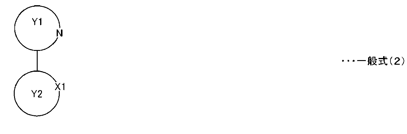
Y1で表わされる芳香族ヘテロ環としては、キノリン環、イソキノリン環、ピリジン環、キノキサリン環、チアゾール環、ピラゾール環、ピリミジン環、ベンゾチアゾール環、オキサゾール環、ベンゾオキサゾール環、インドール環、イソインドール環などがあげられる。Y2で表わされる芳香族炭化水素環または芳香族ヘテロ環としては、Y1にある芳香族ヘテロ環のほかに、ベンゼン環、ナフタレン環、アントラセン環、チオフェン環、ベンゾチオフェン環、フラン環、ベンゾフラン環、フルオレン環、ベンゾピラン環などがあげられる。前記芳香族ヘテロ環や芳香族炭化水素環に機能性基以外の置換基が付加されても構わない。置換基はたとえば、アルキル基(メチル基、エチル基)、置換アルキル基(トリフルオロメチル基)、アルコキシ基(メトキシ基)、ハロゲン原子(フッ素、塩素)、アミノ基、フェニル基などである。
Examples of the aromatic heterocycle represented by Y1 include quinoline ring, isoquinoline ring, pyridine ring, quinoxaline ring, thiazole ring, pyrazole ring, pyrimidine ring, benzothiazole ring, oxazole ring, benzoxazole ring, indole ring, isoindole ring, etc. Is given. As the aromatic hydrocarbon ring or aromatic heterocycle represented by Y2, in addition to the aromatic heterocycle in Y1, benzene ring, naphthalene ring, anthracene ring, thiophene ring, benzothiophene ring, furan ring, benzofuran ring, Examples thereof include a fluorene ring and a benzopyran ring. Substituents other than functional groups may be added to the aromatic heterocycle or aromatic hydrocarbon ring. Examples of the substituent include an alkyl group (methyl group, ethyl group), a substituted alkyl group (trifluoromethyl group), an alkoxy group (methoxy group), a halogen atom (fluorine, chlorine), an amino group, and a phenyl group.
一般式(1)におけるL2はL1に含まれるものでもよいが、そのほかにアセチルアセトナート誘導体、ピコリネート誘導体、テトラキスピラゾリルボレート誘導体があげられる。
L2 in the general formula (1) may be contained in L1, but other examples include acetylacetonate derivatives, picolinate derivatives, and tetrakispyrazolyl borate derivatives.
青色ドーパントの固形分の濃度は10wt%以上30wt%以下が望ましく、緑色ドーパントの固形分の濃度は10wt%未満が望ましく、また、赤色ドーパントの固形分の濃度は10wt%未満が望ましい。発光ドーパントの重量平均分子量は500以上3000以下が望ましい。
The solid concentration of the blue dopant is desirably 10 wt% or more and 30 wt% or less, the solid content of the green dopant is desirably less than 10 wt%, and the solid content of the red dopant is desirably less than 10 wt%. The weight average molecular weight of the luminescent dopant is preferably 500 or more and 3000 or less.
<機能性基>
発光ドーパントの分子には、平面状、棒状、正四面体状、正八面体状、球状など様々な形状の分子が存在する。これらの分子に適切な機能性基を付加することで、基板面に対し略水平に配向させることができる。分子を配向させることによって、遷移双極子モーメントの配向を制御する。 <Functional group>
The luminescent dopant molecule has various shapes such as a planar shape, a rod shape, a regular tetrahedral shape, a regular octahedral shape, and a spherical shape. By adding an appropriate functional group to these molecules, it can be oriented substantially horizontally with respect to the substrate surface. By orienting the molecules, the orientation of the transition dipole moment is controlled.
「略水平に配向」とは、分子の平均値の基板面に対する水平方向成分が、垂直方向成分より大きくなることをいう。このとき、例えば平面状分子に注目した場合、平面状分子の平均値の基板面に対する水平方向成分が、垂直方向成分より大きくなっている。また、棒状分子に注目した場合、棒状分子の長軸の平均値の基板面に対する水平方向成分が、垂直方向成分より大きくなっている。なお、平面状分子とは例えば前記した縮合多環芳香族化合物や、一般式(1)で示される4配位金属錯体、また棒状分子とは短辺長と長辺長とのアスペクト比(短辺/長辺)が0.05~0.3の範囲にあるものをいう。
“Substantially horizontally oriented” means that the horizontal component of the average value of molecules with respect to the substrate surface is larger than the vertical component. At this time, for example, when attention is paid to planar molecules, the horizontal component of the average value of the planar molecules with respect to the substrate surface is larger than the vertical component. When attention is paid to rod-like molecules, the horizontal component of the average value of the long axes of the rod-like molecules with respect to the substrate surface is larger than the vertical component. The planar molecule is, for example, the above-mentioned condensed polycyclic aromatic compound, the tetracoordinate metal complex represented by the general formula (1), or the rod-like molecule is an aspect ratio (short side length to short side length). (Side / long side) is in the range of 0.05 to 0.3.
発光ドーパントである平面分子または棒状分子に適切な機能性基を付加することで、基板面に対し略水平に配向させることができる。
By adding an appropriate functional group to a planar molecule or rod-like molecule that is a luminescent dopant, it can be oriented substantially horizontally with respect to the substrate surface.
一般式(1)で示される金属錯体においては、2座配位子L1、L2のいずれか一方、または両方に機能性基を付加する。機能性基としては表面エネルギーが小さいものもしくは下地層との相互作用が大きいものが好ましい。表面エネルギーが小さい機能性基を用いた場合には、成膜中に機能性基としては表面エネルギーが小さいフルオロアルキル基、パーフルオロアルキル基、アルキル基(ただしCの数が10以上)、パーフルオロポリエーテル基、シロキシ基(-Si-O-Si-)が挙げられる。表面エネルギーを考慮すれば、フルオロアルキル基、パーフルオロポリエーテル基が望ましく、パーフルオロアルキル基がさらに望ましい。フッ素を有する置換基では、フッ素の数が多いほど膜表面へと移動する作用が強い。具体的には、置換基に存在するフッ素の数が7以上であることが望ましい。これらの基は(化8)のように主骨格に直接導入してもよいが、結合角を考慮すると(化9)のようにアミド結合やエステル結合などを介して導入した方がより好ましい。
In the metal complex represented by the general formula (1), a functional group is added to one or both of the bidentate ligands L1 and L2. As the functional group, those having a small surface energy or those having a large interaction with the underlayer are preferable. When a functional group having a low surface energy is used, a functional group having a low surface energy is a fluoroalkyl group, a perfluoroalkyl group, an alkyl group (however, the number of C is 10 or more), perfluoro, and the like. Examples thereof include a polyether group and a siloxy group (—Si—O—Si—). Considering the surface energy, a fluoroalkyl group and a perfluoropolyether group are desirable, and a perfluoroalkyl group is more desirable. In the substituent having fluorine, the larger the number of fluorine, the stronger the action of moving to the film surface. Specifically, the number of fluorines present in the substituent is desirably 7 or more. These groups may be introduced directly into the main skeleton as in (Chemical Formula 8), but it is more preferable to introduce them through an amide bond or an ester bond as in (Chemical Formula 9) in consideration of the bond angle.

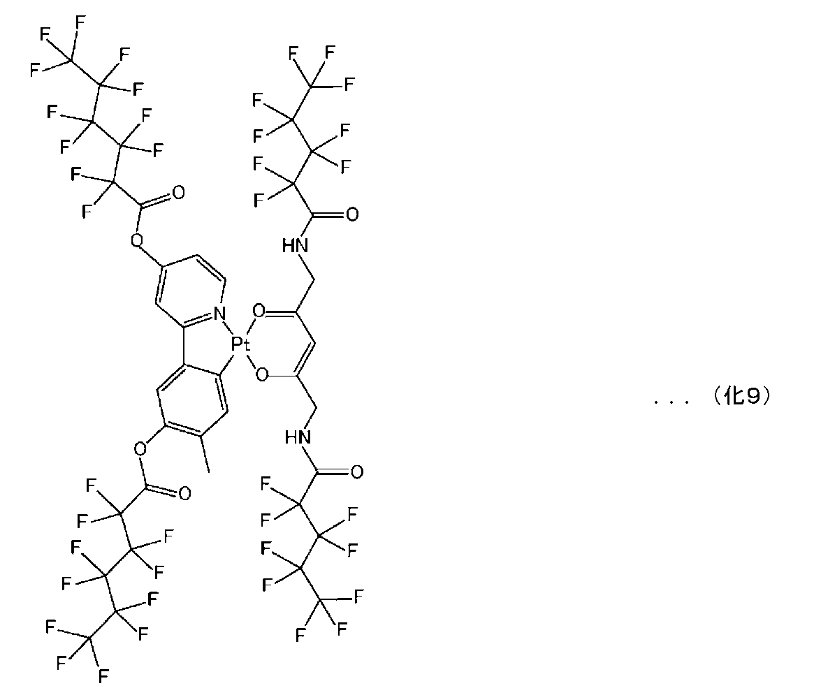
また下地層との相互作用が大きい機能性基としてはフェニルアミノ基、オキサゾール基、カルバゾール基、ヒドラゾン部位といった下地層(例えば正孔輸送層や電子輸送層など)と類似の構造であるものや、ヒドロキシ基(-OH)、チオール基(-SH)、カルボキシル基(-COOH)、スルホ基(-SO3H)、I、Br、Cl、F、SCN、CN、NH2、NO2、ビピリジル基があげられる。これらの基は、主骨格に直接導入してもよいが、分子の大きさや結合角を考慮し、(化10)のようにアルキル鎖などを介して導入したほうが好ましい。
In addition, as a functional group having a large interaction with the underlayer, a functional group having a similar structure to an underlayer (such as a hole transport layer or an electron transport layer) such as a phenylamino group, an oxazole group, a carbazole group, or a hydrazone site, Hydroxy group (—OH), thiol group (—SH), carboxyl group (—COOH), sulfo group (—SO 3 H), I, Br, Cl, F, SCN, CN, NH 2 , NO 2 , bipyridyl group Can be given. These groups may be introduced directly into the main skeleton, but are preferably introduced via an alkyl chain or the like as in (Chemical Formula 10) in consideration of the size of the molecule and the bond angle.
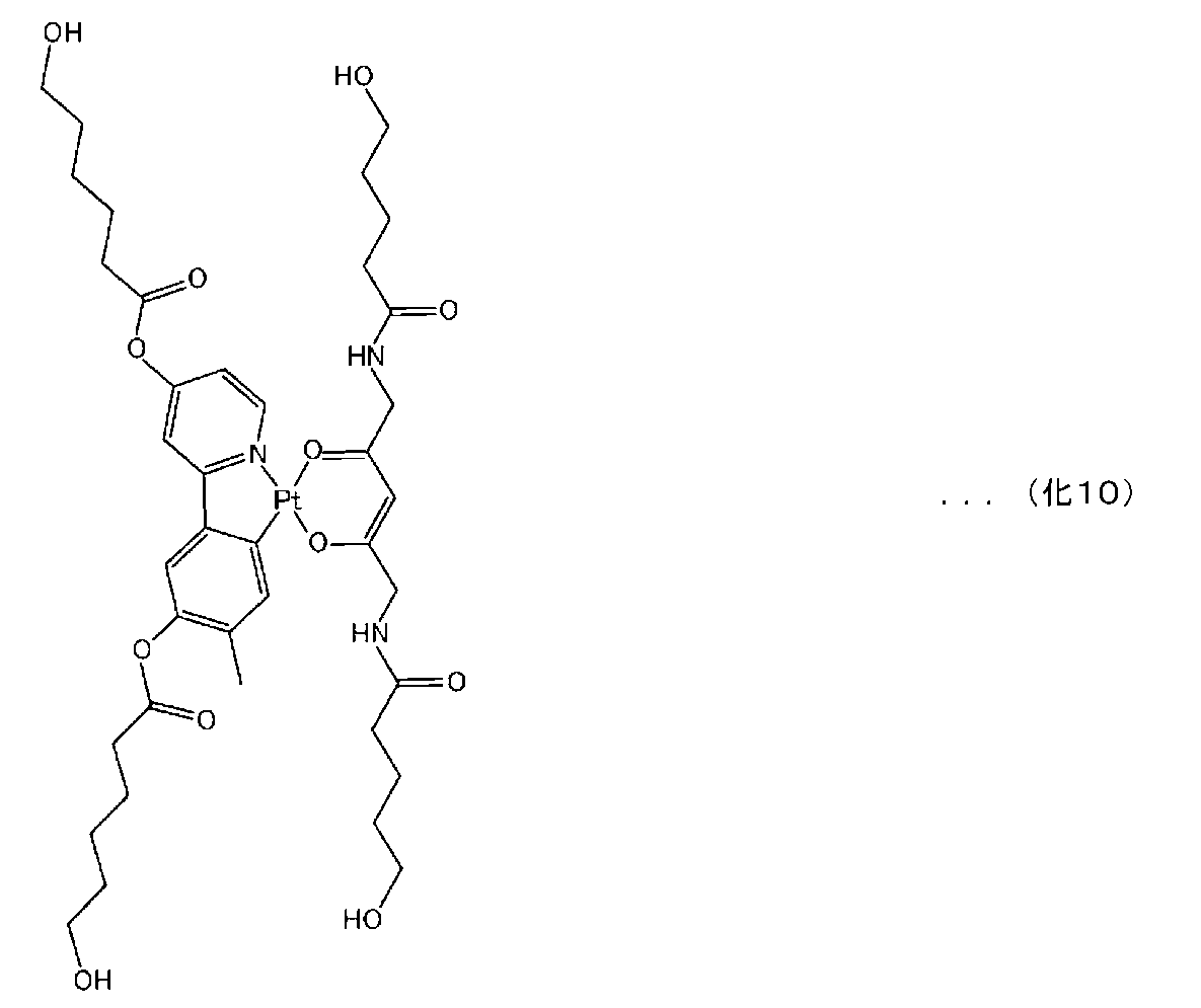
上記機能性基はドーパントに2つ以上付加する必要がある。平面状分子の場合には4つ付加することが好ましい。機能性基は棒状分子の場合には分子の両末端に付加する。平面分子の場合には例えば(化11)のように分子の重心を通る直線の両端に付加する。平面分子の場合には(化12)のように4つの機能性基を付加することでより水平に配向させることができる。
It is necessary to add two or more functional groups to the dopant. In the case of a planar molecule, it is preferable to add four. In the case of a rod-like molecule, the functional group is added to both ends of the molecule. In the case of a planar molecule, for example, it is added to both ends of a straight line passing through the center of gravity of the molecule as shown in (Chem. In the case of a planar molecule, it can be oriented more horizontally by adding four functional groups as shown in (Chemical Formula 12).


<配向制御原理>
物質の表面は一般に内部(バルク)と異なり片側に同種の分子が存在しないため引力が働かずエネルギーが高く不安定である。そのため、表面エネルギーを低下させるために表面積を小さくするように変形させる力(表面張力)が働く。また、物質内に表面エネルギーの低い官能基を有する分子がある場合には、その官能基を表面に出すことで表面エネルギーを低下させ、安定化する。例えば、水と界面活性剤(両親媒性分子)の場合、界面活性剤は表面エネルギーの低い官能基である疎水基を分子内に有し、その疎水基を水面から出す形で水面に単分子膜を形成することで水面の表面エネルギー低下させている。 <Orientation control principle>
Unlike the inside (bulk), the surface of a substance is generally unstable because of the absence of the same kind of molecules on one side and no attractive force. Therefore, a force (surface tension) for deforming the surface area to reduce the surface energy acts. In addition, when there is a molecule having a functional group with low surface energy in the substance, the surface energy is lowered and stabilized by exposing the functional group to the surface. For example, in the case of water and a surfactant (amphiphilic molecule), the surfactant has a hydrophobic group, which is a functional group having a low surface energy, in the molecule, and a single molecule is formed on the surface of the water in such a way that the hydrophobic group is released from the water surface. The surface energy of the water surface is reduced by forming a film.
本発明の分子は分子内にフルオロアルキル基などの表面エネルギーが低い官能基を有している。ベンゼン環などの部位はそれよりも表面エネルギーが高い。膜が形成される際には、表面エネルギーを小さくするために、上記表面エネルギーの低い官能基を表面に出すように力が働く。(化12)のように機能性基を付加した分子ではこの作用により表面エネルギーの低い官能基を膜表面に移動させることで分子面を基板面に対しおおむね水平に配向させることができる。
The molecule of the present invention has a functional group with low surface energy such as a fluoroalkyl group in the molecule. Sites such as the benzene ring have higher surface energy. When a film is formed, a force acts to bring out the functional group having a low surface energy on the surface in order to reduce the surface energy. In a molecule to which a functional group is added as in (Chemical Formula 12), the molecular surface can be oriented almost horizontally with respect to the substrate surface by moving a functional group having a low surface energy to the film surface by this action.
また下地層と相互作用を利用する場合には、下地層と機能性基の間に働く、分子間力、水素結合、配位結合の作用により機能性基が下地層に引き寄せられる。(化5)のように機能性基を付加した場合にはこの作用により分子面を基板面に対しておおむね水平に配向させることができる。
In the case of utilizing the interaction with the underlayer, the functional group is attracted to the underlayer by the action of intermolecular force, hydrogen bond, and coordinate bond acting between the underlayer and the functional group. When a functional group is added as in (Chemical Formula 5), the molecular surface can be oriented almost horizontally with respect to the substrate surface by this action.
有機分子の配向状態は、入射角を変化させながらIRスペクトル、あるいはラマンスペクトルを測定することで調べることができる。
The orientation state of the organic molecule can be examined by measuring the IR spectrum or the Raman spectrum while changing the incident angle.
また遷移双極子モーメントの方向は、公知の方法で評価することができる。例えば(APPLIED PHYSICS LETTERS 96、073302(2010).)、フォトルミネッセンスのP偏光成分の放射角度依存性を、有機発光装置に光学接触させた半球レンズ・シリンドリカルレンズを用いて、薄膜デバイスの干渉効果を除いた上で、実験的に測定し、計算機シミュレーションと比較することで、遷移双極子モーメントにおける水平方向成分と垂直方向成分の各々の割合を求めることができる。これはP偏光強度の角度依存性が水平成分と垂直成分の割合により決まることによる(S偏光は水平成分のみから成る)。通常の発光層を構成する有機分子の配向はランダム(等方的)であり、その為、遷移双極子モーメントの構成成分の割合は水平成分・垂直成分共に50%である。
Also, the direction of the transition dipole moment can be evaluated by a known method. For example (APPLIED PHYSICS LETTERS 96, 073302 (2010).) Using the hemispherical lens / cylindrical lens optically contacting the organic light-emitting device to determine the radiation angle dependency of the P-polarized component of photoluminescence Then, the ratio of each of the horizontal component and the vertical component in the transition dipole moment can be obtained by experimental measurement and comparison with computer simulation. This is because the angle dependence of the P-polarized light intensity is determined by the ratio between the horizontal component and the vertical component (S-polarized light consists of only the horizontal component). The orientation of the organic molecules constituting the normal light emitting layer is random (isotropic), and therefore the proportion of the constituent components of the transition dipole moment is 50% for both the horizontal component and the vertical component.
図8に遷移双極子モーメントの方向(水平成分の割合)(%)と励起子エネルギーの内、可視光に変換される割合(%)の関係の計算結果を示す。計算は自作の有機デバイスシミュレータを用いたもので、光学薄膜干渉効果及び表面プラズモン等の電気双極子と金属界面の近接場相互作用を考慮したものである。構造はアルミ反射電極(上部電極、膜厚150nm)、有機発光層(膜厚250nm)、ITO透明電極(下部電極、膜厚150nm)、ガラス基板(BK7、厚さ0.7mm)である。上部電極、下部電極、ガラス基板の屈折率は実測値を用い、有機発光層の屈折率は、典型的な発光層の屈折率に合わせて、1.8とした。また発光位置は上部電極から75nmの位置に設定し、発光波長は550nmとした。
Fig. 8 shows the calculation result of the relationship between the direction of transition dipole moment (ratio of horizontal component) (%) and the ratio of exciton energy converted to visible light (%). The calculation is based on a self-made organic device simulator that takes into account the optical thin film interference effect and near-field interaction between the electric dipole such as surface plasmon and the metal interface. The structure is an aluminum reflective electrode (upper electrode, film thickness 150 nm), an organic light emitting layer (film thickness 250 nm), an ITO transparent electrode (lower electrode, film thickness 150 nm), and a glass substrate (BK7, thickness 0.7 mm). The measured values were used for the refractive indexes of the upper electrode, the lower electrode, and the glass substrate, and the refractive index of the organic light emitting layer was set to 1.8 in accordance with the refractive index of a typical light emitting layer. The emission position was set at a position 75 nm from the upper electrode, and the emission wavelength was 550 nm.
図8より、水平成分が50%の時の励起子エネルギーの内、可視光に変換される割合の値は、水平成分が50%より大きい(好ましくは60%以上の)場合に、水平成分が100%になるまで単調に増大した。これは水平成分の遷移双極子モーメントをもたらす電気双極子放射場が表面プラズモンポラリトンを殆ど励起出来ないことからも妥当な結果である。
From FIG. 8, the value of the ratio of exciton energy when the horizontal component is 50% is converted to visible light when the horizontal component is greater than 50% (preferably 60% or more). It increased monotonically until it reached 100%. This is a reasonable result because the electric dipole radiation field that causes the transition dipole moment of the horizontal component can hardly excite surface plasmon polaritons.
発光位置(金属電極からの距離、0nmから250nm)や波長(380nmから780nm)を変化させると水平成分が50%の時の励起子エネルギーの内、可視光に変換される割合の値は75%から増減するが何れの場合も水平成分が50%より大きい(好ましくは60%以上の)場合に、水平成分が100%になるまで単調に、励起子エネルギーの内、可視光に変換される割合(%)が増大した。
When the light emission position (distance from the metal electrode, 0 nm to 250 nm) and wavelength (380 nm to 780 nm) are changed, the ratio of the exciton energy when the horizontal component is 50% is converted to visible light is 75%. In any case, when the horizontal component is greater than 50% (preferably 60% or more), the ratio of the exciton energy that is converted to visible light monotonically until the horizontal component reaches 100%. (%) Increased.
<ホスト>
ホストとして、カルバゾール誘導体、フルオレン誘導体またはアリールシラン誘導体などを用いることが好ましい。効率の良い発光を得るためには青色ドーパントの励起エネルギーよりも、ホストの励起エネルギーが十分大きいことが好ましい。なお、励起エネルギーは発光スペクトルを用いて測定される。 <Host>
As the host, it is preferable to use a carbazole derivative, a fluorene derivative, an arylsilane derivative, or the like. In order to obtain efficient light emission, it is preferable that the excitation energy of the host is sufficiently larger than the excitation energy of the blue dopant. The excitation energy is measured using an emission spectrum.
ホストとして、カルバゾール誘導体、フルオレン誘導体またはアリールシラン誘導体などを用いることが好ましい。効率の良い発光を得るためには青色ドーパントの励起エネルギーよりも、ホストの励起エネルギーが十分大きいことが好ましい。なお、励起エネルギーは発光スペクトルを用いて測定される。 <Host>
As the host, it is preferable to use a carbazole derivative, a fluorene derivative, an arylsilane derivative, or the like. In order to obtain efficient light emission, it is preferable that the excitation energy of the host is sufficiently larger than the excitation energy of the blue dopant. The excitation energy is measured using an emission spectrum.
<陰極>
陰極材料は、発光層303からの光を反射するための反射電極である。具体的には、LiFとAlの積層体やMg:Ag合金などが好適に用いられる。また、これらの材料に限定されるものではなく、例えばLiFの代わりとして、Cs化合物、Ba化合物、Ca化合物などを用いることができる。 <Cathode>
The cathode material is a reflective electrode for reflecting light from thelight emitting layer 303. Specifically, a laminate of LiF and Al, an Mg: Ag alloy, or the like is preferably used. Moreover, it is not limited to these materials, For example, a Cs compound, Ba compound, Ca compound etc. can be used instead of LiF.
陰極材料は、発光層303からの光を反射するための反射電極である。具体的には、LiFとAlの積層体やMg:Ag合金などが好適に用いられる。また、これらの材料に限定されるものではなく、例えばLiFの代わりとして、Cs化合物、Ba化合物、Ca化合物などを用いることができる。 <Cathode>
The cathode material is a reflective electrode for reflecting light from the
次に、本発明の具体的な実施例を説明する。本発明が以下の実施例に限定されるものでないことは先述の通りである。
Next, specific examples of the present invention will be described. As described above, the present invention is not limited to the following examples.
本発明の第6の実施例として図3に示す構造の白色発光素子を作製した。下部電極にはITO電極、正孔注入層にはPEDOTをスピンコート法にて形成した。正孔輸送層にはポリマー系の材料を用いた。有機発光層はホストとしてmCP(1、3-ビス(カルバゾル-9-イル)ベンゼン)、青色ドーパントには(化10)、赤色ドーパントには(化12)、緑色ドーパントには(化13)を用いた。
As a sixth example of the present invention, a white light emitting device having the structure shown in FIG. 3 was produced. An ITO electrode was formed on the lower electrode, and PEDOT was formed on the hole injection layer by spin coating. A polymer material was used for the hole transport layer. The organic light-emitting layer contains mCP (1,3-bis (carbazol-9-yl) benzene) as a host, (Chemical Formula 10) for a blue dopant, (Chemical Formula 12) for a red dopant, and (Chemical Formula 13) for a green dopant. Using.
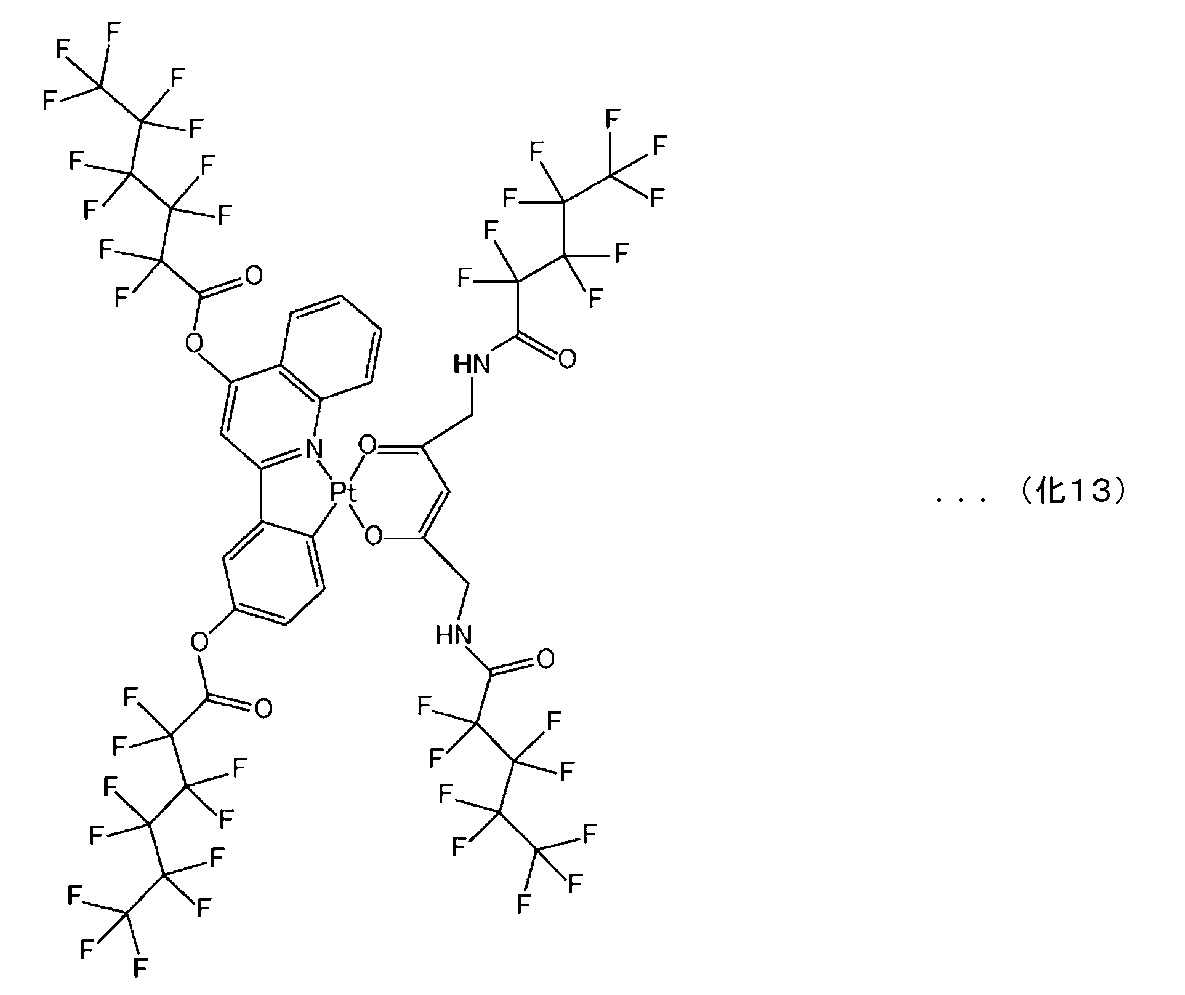
それぞれの材料の重量比は100:10:0.5:0.5とした。これらのホスト、青色、赤色、緑色ドーパントをトルエンに溶解させて塗液を作製した。この塗液を用いて、スピンコート法により有機発光層を形成した。続いて電子輸送層としてUGH2および3TPYMBの層を真空蒸着法で形成した。次にLiFとAlの積層体を上部電極として形成し、目的の有機発光素子を作製した。発光位置は各色ドーパントとも上部電極から75nm近傍となるようにした。
The weight ratio of each material was 100: 10: 0.5: 0.5. These host, blue, red, and green dopants were dissolved in toluene to prepare a coating solution. Using this coating liquid, an organic light emitting layer was formed by spin coating. Subsequently, UGH2 and 3TPYMB layers were formed as an electron transport layer by a vacuum deposition method. Next, a laminate of LiF and Al was formed as the upper electrode, and the target organic light emitting device was produced. The emission position of each color dopant was set to be around 75 nm from the upper electrode.
作製した有機発光素子に電圧を印加したところ、3つのドーパントからの発光がELスペクトルから確認され、白色発光が確認できた。また、比較例6として機能性基を付加しないドーパントを用いた素子を作製した。実施例6は比較例6と比較して1.30倍高い発光効率を示した。なお、実施例6と同様の構成の発光層を別途試作し、フォトルミネッセンス測定において、P偏光強度の角度依存性を測定し、各色ドーパントの遷移双極子モーメントの構成成分の割合を調べたところ、各色とも水平成分が85%以上であった。他方で、比較例6においては各色とも水平成分が約50%であった。
When a voltage was applied to the produced organic light emitting device, light emission from the three dopants was confirmed from the EL spectrum, and white light emission was confirmed. Moreover, the element using the dopant which does not add a functional group as the comparative example 6 was produced. Example 6 showed a luminous efficiency 1.30 times higher than that of Comparative Example 6. In addition, when a light emitting layer having the same configuration as that of Example 6 was separately prototyped, and the photoluminescence measurement was performed, the angle dependency of the P-polarized light intensity was measured, and the ratio of the constituent components of the transition dipole moment of each color dopant was examined. The horizontal component of each color was 85% or more. On the other hand, in Comparative Example 6, the horizontal component of each color was about 50%.
なお、本明細書の前半部で説明したように、遷移双極子モーメントの方向が等方的である場合、励起子エネルギーの約75%が可視光に変換され、25%が表面プラズモンポラリトンに由来する損失となる。従って遷移双極子モーメントの方向が等方的である比較例1に対して、遷移双極子モーメントの方向が略水平である実施例6の発光効率が1.30(<(25+75)/75≒1.33)倍であるということは、表面プラズモンポラリトンによる損失の大半が可視光に変換されたためと考えられ、効率向上としては上限に近い十分大きな値である。
As described in the first half of this specification, when the direction of the transition dipole moment is isotropic, about 75% of the exciton energy is converted to visible light, and 25% is derived from the surface plasmon polariton. Loss. Therefore, in contrast to Comparative Example 1 in which the direction of the transition dipole moment is isotropic, the luminous efficiency of Example 6 in which the direction of the transition dipole moment is substantially horizontal is 1.30 (<(25 + 75) / 75≈1. .33) is considered to be because most of the loss due to the surface plasmon polariton was converted into visible light, which is a sufficiently large value close to the upper limit for improving efficiency.
本発明の第7の実施例として、複数の有機発光素子を接続した光源装置を作製した。作製した素子は、実施例1と同様の層構成で、発光層にホストと赤色ドーパントとして(化12)、緑色ドーパントとして(化14)を含む素子(RG素子)と発光層にホストと青色ドーパントとして(化9)を含む素子(B素子)を面内に作りわけ、各素子を直列および並列に接続した。塗布膜の作製にはインクジェット法を用いた。発光位置は各色ドーパントとも上部電極から75nm近傍となるようにした。
As a seventh example of the present invention, a light source device in which a plurality of organic light emitting elements were connected was produced. The fabricated device has the same layer structure as in Example 1, with the light-emitting layer including a host and a red dopant (Chemical Formula 12), and a green dopant (Chemical Formula 14) and a light-emitting layer including a host and a blue dopant. The element (B element) including (Chemical Formula 9) was made in-plane, and each element was connected in series and in parallel. An inkjet method was used for producing the coating film. The emission position of each color dopant was set to be around 75 nm from the upper electrode.
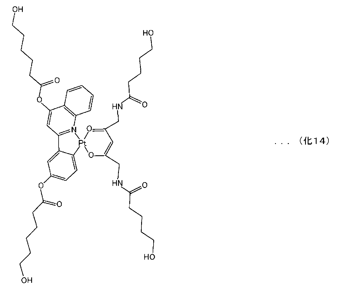
均質な白色光を得るために、作製した素子の発光面に拡散板を取り付けた。作製した光源装置では良好な白色光が得られた。また、比較例7として機能性基を付加しないドーパントを用いた素子を作製した。実施例7は比較例7と比較して1.22倍高い発光効率を示した。なお、実施例2と同様の構成の発光層を別途試作し、フォトルミネッセンス測定において、P偏光強度の角度依存性を測定し、各色ドーパントの遷移双極子モーメントの構成成分の割合を調べたところ、各色とも水平成分が83%以上であった。他方で、比較例7においては各色とも水平成分が約50%であった。
In order to obtain uniform white light, a diffusion plate was attached to the light emitting surface of the fabricated element. In the produced light source device, good white light was obtained. Moreover, the element using the dopant which does not add a functional group as the comparative example 7 was produced. Example 7 showed a luminous efficiency 1.22 times higher than that of Comparative Example 7. In addition, when a light emitting layer having the same configuration as that of Example 2 was separately prototyped, in the photoluminescence measurement, the angle dependency of the P-polarized light intensity was measured, and the ratio of the constituent components of the transition dipole moment of each color dopant was examined. The horizontal component of each color was 83% or more. On the other hand, in Comparative Example 7, the horizontal component of each color was about 50%.
実施例6と同様に、発光効率が1.22倍であるということは、表面プラズモンポラリトンによる損失のかなりの割合が可視光に変換されたためと考えられ、効率向上としては上限に近い十分大きな値である。
As in Example 6, the fact that the luminous efficiency is 1.22 times is considered that a considerable proportion of the loss due to the surface plasmon polariton was converted to visible light, and a sufficiently large value close to the upper limit for improving the efficiency. It is.
また拡散板をつけることにより、発光層において励起子エネルギーから変換され、発生した可視光の内の、より多くを外部(空気)へと取出すことができる。従って、遷移双極子モーメントの方向が略水平であることによる効率向上効果がさらに増幅され、より発光効率の高い光源装置を得ることが出来る。
Also, by attaching a diffuser plate, it is possible to extract more of the visible light generated from the exciton energy converted in the light emitting layer to the outside (air). Therefore, the efficiency improvement effect due to the direction of the transition dipole moment being substantially horizontal is further amplified, and a light source device with higher luminous efficiency can be obtained.
本発明の第8の実施例として、複数の有機発光素子を接続した光源装置を作製した。作製した素子は、実施例6と同様の層構成で、発光層にホストと赤色ドーパントとして(化12)を含む素子(R素子)と、発光層にホスト材料と緑色ドーパントとして(化13)を含む素子(G素子)と発光層にホストと青色ドーパントとして(化9)を含む素子(B素子)を面内に作りわけ、各素子を直列および並列に接続した。塗布膜の作製にはインクジェット法を用いた。発光位置は各色ドーパントとも上部電極から75nm近傍となるようにした。均質な白色光を得るために、作製した素子の発光面に拡散板を取り付けた。作製した光源装置では良好な白色光が得られた。また、比較例6として機能性基を付加しないドーパントを用いた素子を作製した。実施例8は比較例38比較して1.20倍高い発光効率を示した。なお、実施例8と同様の構成の発光層を別途試作し、フォトルミネッセンス測定において、P偏光強度の角度依存性を測定し、各色ドーパントの遷移双極子モーメントの構成成分の割合を調べたところ、各色とも水平成分が88%以上であった。他方で、比較例8においては各色とも水平成分が約50%であった。
As an eighth example of the present invention, a light source device in which a plurality of organic light emitting elements were connected was produced. The manufactured device has the same layer structure as in Example 6, and includes a device (R device) including (Chemical Formula 12) as a host and a red dopant in the light emitting layer, and a chemical material (Chemical Formula 13) as the host material and green dopant in the light emitting layer. An element (G element) including a host and a blue dopant (Chemical element 9) as a blue dopant in the light emitting layer was prepared in-plane, and the elements were connected in series and in parallel. An inkjet method was used for producing the coating film. The emission position of each color dopant was set to be around 75 nm from the upper electrode. In order to obtain uniform white light, a diffusion plate was attached to the light emitting surface of the fabricated device. In the produced light source device, good white light was obtained. Moreover, the element using the dopant which does not add a functional group as the comparative example 6 was produced. In Example 8, the luminous efficiency was 1.20 times higher than that in Comparative Example 38. In addition, when a light emitting layer having the same configuration as that of Example 8 was separately prototyped, and the photoluminescence measurement was performed to measure the angle dependency of the P-polarized light intensity, and the proportion of the constituent components of the transition dipole moment of each color dopant was examined, The horizontal component of each color was 88% or more. On the other hand, in Comparative Example 8, the horizontal component of each color was about 50%.
実施例6と同様に、発光効率が1.20倍であるということは、表面プラズモンポラリトンによる損失のかなりの割合が可視光に変換されたためと考えられ、効率向上としては十分大きな値である。
As in Example 6, the fact that the luminous efficiency is 1.20 times is considered that a considerable proportion of the loss due to the surface plasmon polariton is converted into visible light, which is a sufficiently large value for improving the efficiency.
また拡散板をつけることにより、発光層において励起子エネルギーから変換され、発生した可視光の内の、より多くを外部(空気)へと取出すことができる。従って、遷移双極子モーメントの方向が略水平であることによる効率向上効果がさらに増幅され、より発光効率の高い光源装置を得ることが出来る。
Also, by attaching a diffuser plate, it is possible to extract more of the visible light generated from the exciton energy converted in the light emitting layer to the outside (air). Therefore, the efficiency improvement effect due to the direction of the transition dipole moment being substantially horizontal is further amplified, and a light source device with higher luminous efficiency can be obtained.
なお、実施例6~実施例8において、発光層303のドーパントが、例えばフルオロアルキル基、パーフルオロアルキル基、アルキル基(Cの数は10以上)、パーフルオロポリエーテル基及びシロキシ基のうちから1つ以上選ばれる機能性基を有することにより、発光層303のドーパントの濃度は、発光層303における電子輸送層304及び上部電極102が存在しない側よりも発光層303における電子輸送層304及び上部電極102が存在する側の方が高くなっている。これは、ドーパントが発光層303における電子輸送層304及び上部電極102が存在する側へ移動することにより生じるものである。
In Examples 6 to 8, the dopant of the light emitting layer 303 is, for example, a fluoroalkyl group, a perfluoroalkyl group, an alkyl group (the number of C is 10 or more), a perfluoropolyether group, or a siloxy group. By having one or more functional groups selected, the dopant concentration of the light emitting layer 303 is higher than the side of the light emitting layer 303 where the electron transport layer 304 and the upper electrode 102 are not present. The side where the electrode 102 exists is higher. This occurs because the dopant moves to the side where the electron transport layer 304 and the upper electrode 102 exist in the light emitting layer 303.
また、実施例6~実施例8において、発光層303のドーパントが、例えば-OH、-SH、-COOH、-SO3H、I、Br、Cl、F、SCN、CN、NH2、NO2及びビピリジル基、フェニルアミノ基、オキサゾール基、カルバゾール基及びヒドラゾン部位のうちから1つ以上選ばれる機能性基を有することにより、発光層303のドーパントの濃度は、発光層303における正孔輸送層302及び下部電極101が存在しない側よりも発光層303における正孔輸送層302及び下部電極101が存在する側の方が高くなっている。これは、ドーパントが発光層303における正孔輸送層302及び下部電極101が存在する側へ移動することにより生じるものである。
In Examples 6 to 8, the dopant of the light emitting layer 303 is, for example, —OH, —SH, —COOH, —SO 3 H, I, Br, Cl, F, SCN, CN, NH 2 , NO 2. And having at least one functional group selected from a bipyridyl group, a phenylamino group, an oxazole group, a carbazole group, and a hydrazone site, the concentration of the dopant in the light-emitting layer 303 can be increased by the hole transport layer 302 in the light-emitting layer 303. And the side where the hole transport layer 302 and the lower electrode 101 exist in the light emitting layer 303 is higher than the side where the lower electrode 101 does not exist. This occurs because the dopant moves to the side where the hole transport layer 302 and the lower electrode 101 exist in the light emitting layer 303.
ここで、発光層303における電子輸送層304及び上部電極102が存在する側とは、それぞれ電子輸送層304及び上部電極102が位置する方向に向かって中央より端部の領域を指す。発光層303における電子輸送層304及び上部電極102が存在しない側とは、それぞれ電子輸送層304及び上部電極102が位置する方向と反対の方向に向かって中央より端部の領域を指す。
Here, the side where the electron transport layer 304 and the upper electrode 102 exist in the light emitting layer 303 refers to a region from the center to the end in the direction in which the electron transport layer 304 and the upper electrode 102 are located, respectively. The side where the electron transport layer 304 and the upper electrode 102 do not exist in the light emitting layer 303 refers to a region from the center to the end in the direction opposite to the direction in which the electron transport layer 304 and the upper electrode 102 are located.
また、発光層303における正孔輸送層302及び下部電極101が存在する側とは、それぞれ正孔輸送層302及び下部電極101が位置する方向に向かって中央より端部の領域を指す。また、発光層303における正孔輸送層302及び下部電極101が存在しない側とは、それぞれ正孔輸送層302及び下部電極101が位置する方向と反対の方向に向かって中央より端部の領域を指す。
Further, the side where the hole transport layer 302 and the lower electrode 101 exist in the light emitting layer 303 refers to a region from the center to the end in the direction in which the hole transport layer 302 and the lower electrode 101 are located, respectively. Further, the side where the hole transport layer 302 and the lower electrode 101 do not exist in the light emitting layer 303 is a region from the center to the opposite direction to the direction in which the hole transport layer 302 and the lower electrode 101 are located, respectively. Point to.
本発明の実施例として、図5に示す光源装置を作製した。光源装置の構成要素である有機発光素子は実施例1と同様の基板100、下部電極101、有機層103、上部電極102からなる。有機発光素子は有機層103が外気から遮断されるように、乾燥剤付きの封止管ガラス501で封止されている。また下部電極101及び上部電極102は、それぞれ配線502を通じて駆動回路503に接続されている。そして、封止管ガラス501付きの有機発光素子及び駆動回路503は筺体505により覆われ、全体として光源装置506となる。なお、駆動回路503はプラグ504を通じて外部電源に接続されることで点灯する。実施例1の有機発光素子を用いた光源装置A及び比較例1の有機発光素子を用いた光源装置Bを作製したところ、光源装置Aは光源装置Bに対して23%の低消費電力化が出来た。
As an example of the present invention, a light source device shown in FIG. 5 was produced. An organic light-emitting element that is a component of the light source device includes a substrate 100, a lower electrode 101, an organic layer 103, and an upper electrode 102 similar to those in the first embodiment. The organic light emitting element is sealed with a sealing tube glass 501 with a desiccant so that the organic layer 103 is shielded from the outside air. The lower electrode 101 and the upper electrode 102 are connected to the drive circuit 503 through the wiring 502, respectively. Then, the organic light emitting element with the sealing tube glass 501 and the drive circuit 503 are covered with a housing 505 to form the light source device 506 as a whole. Note that the drive circuit 503 is lit by being connected to an external power source through the plug 504. When the light source device A using the organic light emitting element of Example 1 and the light source device B using the organic light emitting element of Comparative Example 1 were produced, the light source device A had 23% lower power consumption than the light source device B. done.
100 基板
101 下部電極
102 上部電極
103 有機層
104 第一のバンク
105 第二のバンク
106 樹脂層
107 封止基板
201 拡散板
202 第一の有機発光素子
203 第二の有機発光素子
301 正孔注入層
302 正孔輸送層
303 発光層
304 電子輸送層
305 電子注入層
501 封止管ガラス
502 配線
503 駆動回路
504 プラグ
505 筐体
506 光源装置 DESCRIPTION OFSYMBOLS 100 Substrate 101 Lower electrode 102 Upper electrode 103 Organic layer 104 First bank 105 Second bank 106 Resin layer 107 Sealing substrate 201 Diffusion plate 202 First organic light emitting element 203 Second organic light emitting element 301 Hole injection layer 302 hole transport layer 303 light emitting layer 304 electron transport layer 305 electron injection layer 501 sealing tube glass 502 wiring 503 drive circuit 504 plug 505 housing 506 light source device
101 下部電極
102 上部電極
103 有機層
104 第一のバンク
105 第二のバンク
106 樹脂層
107 封止基板
201 拡散板
202 第一の有機発光素子
203 第二の有機発光素子
301 正孔注入層
302 正孔輸送層
303 発光層
304 電子輸送層
305 電子注入層
501 封止管ガラス
502 配線
503 駆動回路
504 プラグ
505 筐体
506 光源装置 DESCRIPTION OF
Claims (30)
- 下部電極と上部電極とを有し、その一方が反射電極、他方が透明電極であり、
前記下部電極と前記上部電極との間に配置され、ホストおよび第一のドーパントを含む発光層とを有し、
前記第一のドーパントには第一の機能性基が含まれ、
前記第一のドーパントについて、遷移双極子モーメントの平均値の基板面に対する垂直方向成分と水平方向成分のうちの一方が他方より大きく、
前記第一のドーパントの濃度について、前記発光層において前記上部電極が存在する側の領域と、前記下部電極が存在する側の領域のうちいずれか一方が、他方の領域より高い有機発光素子。 A lower electrode and an upper electrode, one of which is a reflective electrode, the other is a transparent electrode,
A light-emitting layer disposed between the lower electrode and the upper electrode and including a host and a first dopant;
The first dopant includes a first functional group,
For the first dopant, one of the vertical component and the horizontal component of the average value of the transition dipole moment with respect to the substrate surface is greater than the other,
Regarding the concentration of the first dopant, in the light emitting layer, one of a region on the side where the upper electrode is present and a region on the side where the lower electrode is present is higher than the other region. - 請求項1において、
前記発光層に含まれるドーパントは平面状分子であり、
前記平面状分子の平均値の基板面に対する垂直方向成分、水平方向成分のうちの一方が他方より大きい有機発光素子。 In claim 1,
The dopant contained in the light emitting layer is a planar molecule,
An organic light emitting device in which one of a vertical direction component and a horizontal direction component of the average value of the planar molecules is larger than the other. - 請求項1において、
前記発光層に含まれるドーパントは棒状分子であり、
前記棒状分子の長軸の平均値の基板面に対する垂直方向成分、水平方向成分のうちの一方が他方より大きい有機発光素子。 In claim 1,
The dopant contained in the light emitting layer is a rod-like molecule,
An organic light emitting device in which one of a vertical component and a horizontal component of the average value of the major axis of the rod-like molecules is larger than the other. - 請求項1において、
前記第一のドーパントについて、遷移双極子モーメントの平均値の基板面に対する垂直方向成分、水平方向性分の一方が60%以上である有機発光素子。 In claim 1,
An organic light-emitting element in which one of a vertical component and a horizontal component of the average value of the transition dipole moment with respect to the substrate surface is 60% or more for the first dopant. - 反射電極と、
透明電極と、
前記反射電極と前記透明電極との間に配置された発光層とを有する有機発光素子であって、
前記発光層にはホスト、第一のドーパントが含まれ、
前記第一のドーパントについて、遷移双極子モーメントの平均値の基板面に対する垂直方向成分が、水平方向成分より大きく、
前記反射電極の前記発光層側に凹凸構造を有する有機発光素子。 A reflective electrode;
A transparent electrode;
An organic light emitting device having a light emitting layer disposed between the reflective electrode and the transparent electrode,
The light emitting layer includes a host, a first dopant,
For the first dopant, the vertical component of the average value of the transition dipole moment with respect to the substrate surface is greater than the horizontal component,
An organic light emitting device having a concavo-convex structure on the light emitting layer side of the reflective electrode. - 請求項5において、
前記第一のドーパントには第一の機能性基が含まれ、
前記第一のドーパントの濃度について、前記発光層において前記上部電極が存在する側の領域と、前記下部電極が存在する側の領域のうちいずれか一方が、他方の領域より高い有機発光素子。 In claim 5,
The first dopant includes a first functional group,
Regarding the concentration of the first dopant, in the light emitting layer, one of a region on the side where the upper electrode is present and a region on the side where the lower electrode is present is higher than the other region. - 請求項5において
前記発光層には第二のドーパントが含まれ、
前記第二のドーパントの発光色は前記第一のドーパントと異なり、
前記第二のドーパントについて、遷移双極子モーメントの平均値の基板面に対する垂直方向成分が、水平方向成分より大きい有機発光素子。 In claim 5
The light emitting layer includes a second dopant,
The emission color of the second dopant is different from the first dopant,
An organic light-emitting device in which the vertical component with respect to the substrate surface of the average value of the transition dipole moment of the second dopant is larger than the horizontal component. - 請求項7において
前記発光層には第三のドーパントが含まれ、
前記第三のドーパントの発光色は、前記第一のドーパントおよび第二のドーパントと異なり、
前記第三のドーパントについて、遷移双極子モーメントの平均値の基板面に対する垂直方向成分が、水平方向成分より大きい有機発光素子。 In claim 7
The light emitting layer includes a third dopant,
The emission color of the third dopant is different from the first dopant and the second dopant,
The organic light-emitting device in which the vertical component of the average value of the transition dipole moment with respect to the substrate surface is greater than the horizontal component for the third dopant. - 請求項5において、
前記第一のドーパントについて、遷移双極子モーメントの平均値の基板面に対する垂直方向成分が60%以上である有機発光素子。 In claim 5,
An organic light-emitting element in which a component perpendicular to the substrate surface of the average value of the transition dipole moment of the first dopant is 60% or more. - 請求項5において、
前記発光層に含まれるドーパントのうちいずれか1つは平面状分子であり、
前記平面状分子の平均値の基板面に対する垂直方向成分が、水平方向成分より大きい有機発光素子。 In claim 5,
Any one of the dopants contained in the light emitting layer is a planar molecule,
An organic light emitting device in which the vertical component of the average value of the planar molecules with respect to the substrate surface is larger than the horizontal component. - 請求項5において
前記発光層に含まれるドーパントのうちいずれか1つは棒状分子であり、
前記棒状分子の長軸の平均値の基板面に対する垂直方向成分が、水平方向成分より大きい有機発光素子。 In claim 5
Any one of the dopants contained in the light emitting layer is a rod-like molecule,
An organic light emitting device in which the vertical component of the average value of the major axis of the rod-shaped molecules with respect to the substrate surface is larger than the horizontal component. - 請求項5において、
前記凹凸構造はAg、Au、CuまたはAlのいずれかを主成分とする有機発光素子。 In claim 5,
The concavo-convex structure is an organic light-emitting element mainly composed of Ag, Au, Cu, or Al. - 請求項5において
前記凹凸構造は凹凸の高さ、幅及びピッチが発光波長より小さい有機発光素子。 In claim 5
The concavo-convex structure is an organic light emitting device having a concavo-convex height, width, and pitch smaller than the emission wavelength. - 請求項13において、
前記凹凸の高さは40~120nmの範囲にある有機発光素子。 In claim 13,
An organic light emitting device in which the height of the unevenness is in the range of 40 to 120 nm. - 請求項5において、
前記透明電極から見て、前記反射電極が存在する位置とは反対側に光取出し層を有する有機発光素子。 In claim 5,
An organic light emitting device having a light extraction layer on a side opposite to a position where the reflective electrode is present when viewed from the transparent electrode. - 上部電極と、
下部電極と、
前記上部電極と前記下部電極との間に配置された発光層とを有する有機発光素子であって、
前記発光層にはホスト、第一のドーパントが含まれ、
前記第一のドーパントには第一の機能性基が含まれ、
前記第一のドーパントの濃度について、前記発光層において前記上部電極が存在する側の領域と、前記下部電極が存在する側の領域のうちいずれか一方が、他方の領域より高く、
前記第一のドーパントについて、遷移双極子モーメントの平均値の基板面に対する水平方向成分が、垂直方向成分より大きい有機発光素子。 An upper electrode;
A lower electrode;
An organic light emitting device having a light emitting layer disposed between the upper electrode and the lower electrode,
The light emitting layer includes a host, a first dopant,
The first dopant includes a first functional group,
Regarding the concentration of the first dopant, one of the region on the side where the upper electrode is present in the light emitting layer and the region on the side where the lower electrode is present is higher than the other region,
An organic light-emitting device in which the horizontal component with respect to the substrate surface of the average value of the transition dipole moment of the first dopant is larger than the vertical component. - 請求項16において、
前記発光層には第二のドーパントが含まれ、
前記第二のドーパントの発光色は前記第一のドーパントと異なり、
前記第二のドーパントには第二の機能性基が含まれ、
前記第二のドーパントの濃度について、前記発光層において前記上部電極が存在する側の領域と、前記下部電極が存在する側の領域のうちいずれか一方が、他方の領域より高く、
前記第二のドーパントについて、遷移双極子モーメントの平均値の基板面に対する水平方向成分が、垂直方向成分より大きい有機発光素子。 In claim 16,
The light emitting layer includes a second dopant,
The emission color of the second dopant is different from the first dopant,
The second dopant includes a second functional group,
Regarding the concentration of the second dopant, one of the region on the side where the upper electrode is present in the light emitting layer and the region on the side where the lower electrode is present is higher than the other region,
An organic light-emitting device in which the horizontal component with respect to the substrate surface of the average value of the transition dipole moment of the second dopant is larger than the vertical component. - 請求項17において、
前記発光層には第三のドーパントが含まれ、
前記第三のドーパントの発光色は、前記第一のドーパントおよび第二のドーパントと異なり、
前記第三のドーパントには第三の機能性基が含まれ、
前記第三のドーパントの濃度について、前記発光層において前記上部電極が存在する側の領域と、前記下部電極が存在する側の領域のうちいずれか一方が、他方の領域より高く、
前記第三のドーパントについて、遷移双極子モーメントの平均値の基板面に対する水平方向成分が、垂直方向成分より大きい有機発光素子。 In claim 17,
The light emitting layer includes a third dopant,
The emission color of the third dopant is different from the first dopant and the second dopant,
The third dopant includes a third functional group,
Regarding the concentration of the third dopant, one of the region on the side where the upper electrode is present in the light emitting layer and the region on the side where the lower electrode is present is higher than the other region,
An organic light-emitting device in which the horizontal component with respect to the substrate surface of the average value of the transition dipole moment of the third dopant is larger than the vertical component. - 請求項16において、
前記第一のドーパントについて、遷移双極子モーメントの平均値の基板面に対する水平方向成分が60%以上である有機発光素子。 In claim 16,
An organic light-emitting device in which the horizontal component of the average value of the transition dipole moment with respect to the substrate surface is 60% or more for the first dopant. - 請求項16において、
前記発光層に含まれるドーパントのうちいずれか1つは平面状分子であり、
前記平面状分子の平均値の基板面に対する水平方向成分が、垂直方向成分より大きい有機発光素子。 In claim 16,
Any one of the dopants contained in the light emitting layer is a planar molecule,
An organic light emitting device in which a horizontal component with respect to a substrate surface of an average value of the planar molecules is larger than a vertical component. - 請求項16において、
前記発光層に含まれるドーパントのうちいずれか1つは棒状分子であり、
前記棒状分子の長軸の平均値の基板面に対する水平方向成分が、垂直方向成分より大きい有機発光素子。 In claim 16,
Any one of the dopants contained in the light emitting layer is a rod-like molecule,
An organic light emitting device in which a horizontal component with respect to a substrate surface of an average value of major axes of the rod-like molecules is larger than a vertical component. - 請求項1乃至21のいずれかにおいて、
前記第一機能性基は、フルオロアルキル基、パーフルオロアルキル基、アルキル基(Cの数は10以上)、パーフルオロポリエーテル基及びシロキシ基、-OH、-SH、-COOH、-SO3H、I、Br、Cl、F、SCN、CN、NH2、NO2及びビピリジル基、フェニルアミノ基、オキサゾール基、カルバゾール基及びヒドラゾン部位のうちから1つ以上選ばれる有機発光素子。 Any one of claims 1 to 21
The first functional group includes a fluoroalkyl group, a perfluoroalkyl group, an alkyl group (the number of C is 10 or more), a perfluoropolyether group and a siloxy group, —OH, —SH, —COOH, —SO 3 H , I, Br, Cl, F, SCN, CN, NH 2 , NO 2, and a bipyridyl group, a phenylamino group, an oxazole group, a carbazole group, and a hydrazone moiety. - 請求項1乃至21のいずれかにおいて、
前記第一のドーパントは4配位の中心金属からなる金属錯体である有機発光素子。 Any one of claims 1 to 21
The organic light-emitting device, wherein the first dopant is a metal complex composed of a tetracoordinate central metal. - 請求項23において、
前記第一のドーパントは一般式(1)で示される有機発光素子。

Said 1st dopant is an organic light emitting element shown by General formula (1).
- 請求項1乃至21のいずれかの有機発光素子を備える光源装置。 A light source device comprising the organic light emitting device according to any one of claims 1 to 21. *
- 反射電極と、透明電極と、前記反射電極と前記透明電極との間に配置された発光層とを有する有機発光素子の製造方法であって、
前記発光層にはホスト、第一のドーパントが含まれ、
前記第一のドーパントについて、遷移双極子モーメントの平均値の基板面に対する垂直方向成分が、水平方向成分より大きく、
前記発光層を塗布で作製し、
前記反射電極の前記発光層側に凹凸構造を形成する有機発光素子の製造方法。 A method for producing an organic light emitting device comprising a reflective electrode, a transparent electrode, and a light emitting layer disposed between the reflective electrode and the transparent electrode,
The light emitting layer includes a host, a first dopant,
For the first dopant, the vertical component of the average value of the transition dipole moment with respect to the substrate surface is greater than the horizontal component,
The light emitting layer is prepared by coating,
A method for producing an organic light emitting device, wherein a concavo-convex structure is formed on the light emitting layer side of the reflective electrode. - 第一の有機発光素子および第二の有機発光素子を備えた光源装置であって、
前記第一の有機発光素子および第二の有機発光素子は、それぞれ、反射電極と、透明電極と、前記反射電極と前記透明電極との間に配置された発光層とを有し、
前記第一の有機発光素子の発光層には第一のホストおよび第一のドーパントが含まれ、
前記第二の有機発光素子の発光層には第ニのホスト、第二のドーパントおよび第三のドーパントが含まれ、
前記第一のドーパント、第二のドーパントおよび第三のドーパントについて、遷移双極子モーメントの平均値の基板面に対する垂直方向成分が、水平方向成分より大きく、
前記反射電極の前記発光層側に凹凸構造を有する光源装置。 A light source device comprising a first organic light emitting element and a second organic light emitting element,
The first organic light emitting device and the second organic light emitting device each have a reflective electrode, a transparent electrode, and a light emitting layer disposed between the reflective electrode and the transparent electrode,
The light emitting layer of the first organic light emitting device includes a first host and a first dopant,
The light emitting layer of the second organic light emitting device includes a second host, a second dopant, and a third dopant,
For the first dopant, the second dopant and the third dopant, the vertical component of the average value of the transition dipole moment with respect to the substrate surface is greater than the horizontal component,
A light source device having a concavo-convex structure on the light emitting layer side of the reflective electrode. - 上部電極と、下部電極と、前記上部電極と前記下部電極との間に配置された発光層とを有する有機発光素子の製造方法であって、
前記発光層にはホスト、第一のドーパントが含まれ、
前記第一のドーパントには第一の機能性基が含まれ、
前記第一のドーパントの濃度について、前記発光層において前記上部電極が存在する側の領域と、前記下部電極が存在する側の領域のうちいずれか一方が、他方の領域より高く、
前記第一のドーパントについて、遷移双極子モーメントの平均値の基板面に対する水平方向成分が、垂直方向成分より大きく、
前記発光層を塗布で作製する有機発光素子の製造方法。 A method of manufacturing an organic light emitting device comprising an upper electrode, a lower electrode, and a light emitting layer disposed between the upper electrode and the lower electrode,
The light emitting layer includes a host, a first dopant,
The first dopant includes a first functional group,
Regarding the concentration of the first dopant, one of the region on the side where the upper electrode is present in the light emitting layer and the region on the side where the lower electrode is present is higher than the other region,
For the first dopant, the horizontal component of the average value of the transition dipole moment with respect to the substrate surface is greater than the vertical component,
The manufacturing method of the organic light emitting element which produces the said light emitting layer by application | coating. - 第一の有機発光素子および第二の有機発光素子を備えた光源装置であって、
前記第一の有機発光素子および第二の有機発光素子は、それぞれ、上部電極と、下部電極と、前記上部電極と前記下部電極との間に配置された発光層とを有し 、
前記第一の有機発光素子の発光層にはホストおよび第一のドーパントが含まれ、
前記第二の有機発光素子の発光層にはホスト、第二のドーパントおよび第三のドーパントが含まれ、
前記第一のドーパントには第一の機能性基が含まれ、
前記第二のドーパントには第二の機能性基が含まれ、
前記第三のドーパントには第三の機能性基が含まれ、
前記第一のドーパント、第二のドーパントおよび第三のドーパントの濃度について、前記発光層において前記上部電極が存在する側の領域と、前記下部電極が存在する側の領域のうちいずれか一方が、他方の領域より高く、
前記第一のドーパント、第二のドーパントおよび第三のドーパントについて、遷移双極子モーメントの平均値の基板面に対する水平方向成分が、垂直方向成分より大きい光源装置。 A light source device comprising a first organic light emitting element and a second organic light emitting element,
The first organic light emitting device and the second organic light emitting device each have an upper electrode, a lower electrode, and a light emitting layer disposed between the upper electrode and the lower electrode.
The light emitting layer of the first organic light emitting device includes a host and a first dopant,
The light emitting layer of the second organic light emitting device includes a host, a second dopant, and a third dopant,
The first dopant includes a first functional group,
The second dopant includes a second functional group,
The third dopant includes a third functional group,
Regarding the concentration of the first dopant, the second dopant, and the third dopant, either one of the region on the side where the upper electrode is present in the light emitting layer and the region on the side where the lower electrode is present, Higher than the other area,
The light source device in which the horizontal component of the average value of the transition dipole moment with respect to the substrate surface is greater than the vertical component for the first dopant, the second dopant, and the third dopant. - 請求項27又は29の光源装置において、
前記第一のドーパントは青色ドーパントであり、
前記第二のドーパントおよび第三のドーパントは、一方が赤色ドーパントであり、他方が緑色ドーパントである光源装置。 The light source device according to claim 27 or 29,
The first dopant is a blue dopant;
One of the second dopant and the third dopant is a red dopant and the other is a green light source device.
Priority Applications (3)
| Application Number | Priority Date | Filing Date | Title |
|---|---|---|---|
| EP12814721.2A EP2736089B1 (en) | 2011-07-19 | 2012-07-03 | Organic light-emitting element, light source device and organic light-emitting element manufacturing method |
| CN201280035417.0A CN103688385B (en) | 2011-07-19 | 2012-07-03 | The manufacture method of organic illuminating element, light supply apparatus and organic illuminating element |
| US14/233,628 US9496516B2 (en) | 2011-07-19 | 2012-07-03 | Organic light-emitting element, light source device and method of manufacturing organic light-emitting element |
Applications Claiming Priority (4)
| Application Number | Priority Date | Filing Date | Title |
|---|---|---|---|
| JP2011157418A JP5659095B2 (en) | 2011-07-19 | 2011-07-19 | ORGANIC LIGHT EMITTING ELEMENT, LIGHT SOURCE DEVICE, AND METHOD FOR PRODUCING ORGANIC LIGHT EMITTING ELEMENT |
| JP2011157417A JP5789439B2 (en) | 2011-07-19 | 2011-07-19 | ORGANIC LIGHT EMITTING ELEMENT, LIGHT SOURCE DEVICE, AND METHOD FOR PRODUCING ORGANIC LIGHT EMITTING ELEMENT |
| JP2011-157418 | 2011-07-19 | ||
| JP2011-157417 | 2011-07-19 |
Publications (1)
| Publication Number | Publication Date |
|---|---|
| WO2013011833A1 true WO2013011833A1 (en) | 2013-01-24 |
Family
ID=47558012
Family Applications (1)
| Application Number | Title | Priority Date | Filing Date |
|---|---|---|---|
| PCT/JP2012/066996 WO2013011833A1 (en) | 2011-07-19 | 2012-07-03 | Organic light-emitting element, light source device and organic light-emitting element manufacturing method |
Country Status (5)
| Country | Link |
|---|---|
| US (1) | US9496516B2 (en) |
| EP (1) | EP2736089B1 (en) |
| CN (1) | CN103688385B (en) |
| TW (1) | TWI559591B (en) |
| WO (1) | WO2013011833A1 (en) |
Cited By (1)
| Publication number | Priority date | Publication date | Assignee | Title |
|---|---|---|---|---|
| CN103254242A (en) * | 2013-05-02 | 2013-08-21 | 太原理工大学 | Polysubstituted phenylquinoline platinum (II) complex as well as preparation method and application thereof |
Families Citing this family (18)
| Publication number | Priority date | Publication date | Assignee | Title |
|---|---|---|---|---|
| WO2010065071A2 (en) | 2008-11-25 | 2010-06-10 | Regents Of The University Of Minnesota | Replication of patterned thin-film structures for use in plasmonics and metamaterials |
| GB2517696A (en) * | 2013-08-27 | 2015-03-04 | Ibm | Nanodevice assemblies |
| GB201414427D0 (en) | 2014-08-14 | 2014-10-01 | Ibm | Memory device and method for thermoelectric heat confinement |
| CN105590944A (en) * | 2014-10-24 | 2016-05-18 | 上海和辉光电有限公司 | OLED flexible display device |
| EP3227935B1 (en) * | 2014-12-02 | 2022-03-02 | Universiteit Gent | Light emission device with anisotropic properties |
| US10134803B2 (en) * | 2015-01-23 | 2018-11-20 | Vuereal Inc. | Micro device integration into system substrate |
| US10847571B2 (en) | 2015-01-23 | 2020-11-24 | Vuereal Inc. | Micro device integration into system substrate |
| US10700120B2 (en) | 2015-01-23 | 2020-06-30 | Vuereal Inc. | Micro device integration into system substrate |
| CN107851586B (en) | 2015-01-23 | 2021-07-06 | 维耶尔公司 | Selective micro device transfer to a receptor substrate |
| CN105118934B (en) * | 2015-09-17 | 2017-03-15 | 京东方科技集团股份有限公司 | Uneven particle layer preparation method, organic electroluminescence device and display device |
| US20170125735A1 (en) * | 2015-10-30 | 2017-05-04 | National Taiwan University | Electroluminescent device |
| CN110114897B (en) * | 2016-12-28 | 2021-08-31 | 柯尼卡美能达株式会社 | Electronic device |
| US11367840B2 (en) | 2018-01-26 | 2022-06-21 | Universal Display Corporation | Organic electroluminescent materials and devices |
| US11177234B2 (en) * | 2018-06-25 | 2021-11-16 | Intel Corporation | Package architecture with improved via drill process and method for forming such package |
| US11217762B2 (en) * | 2018-11-30 | 2022-01-04 | Universal Display Corporation | Surface-plasmon-pumped light emitting devices |
| KR20200076969A (en) * | 2018-12-20 | 2020-06-30 | 엘지디스플레이 주식회사 | Lighting apparatus using organic light emitting diode |
| CN111384266A (en) * | 2018-12-29 | 2020-07-07 | 广东聚华印刷显示技术有限公司 | Top-emitting electroluminescent device and manufacturing method thereof |
| KR20210136224A (en) | 2020-05-06 | 2021-11-17 | 삼성디스플레이 주식회사 | Llight emitting device and electronic apparatus comprising same |
Citations (7)
| Publication number | Priority date | Publication date | Assignee | Title |
|---|---|---|---|---|
| JPH11102783A (en) | 1997-09-26 | 1999-04-13 | Mitsubishi Electric Corp | Organic electroluminescence element and manufacture thereof |
| JP2001155866A (en) * | 1999-11-24 | 2001-06-08 | Fuji Photo Film Co Ltd | Electroluminescent display |
| JP2004342336A (en) | 2003-05-13 | 2004-12-02 | Semiconductor Energy Lab Co Ltd | Light emitting device and manufacturing method of same |
| JP2007035430A (en) | 2005-07-27 | 2007-02-08 | Seiko Instruments Inc | Organic light emitting device |
| JP2008210717A (en) * | 2007-02-27 | 2008-09-11 | Toppan Printing Co Ltd | Organic electroluminescent device |
| WO2011043083A1 (en) * | 2009-10-09 | 2011-04-14 | 出光興産株式会社 | Organic electroluminescence element |
| WO2011132773A1 (en) * | 2010-04-22 | 2011-10-27 | 出光興産株式会社 | Organic electroluminescent element and lighting device |
Family Cites Families (5)
| Publication number | Priority date | Publication date | Assignee | Title |
|---|---|---|---|---|
| US6696177B1 (en) | 2000-08-30 | 2004-02-24 | Eastman Kodak Company | White organic electroluminescent devices with improved stability and efficiency |
| JP4984343B2 (en) | 2000-09-29 | 2012-07-25 | 株式会社日立製作所 | Organic electroluminescent device and optoelectronic device using the same |
| TWI225312B (en) | 2001-02-08 | 2004-12-11 | Semiconductor Energy Lab | Light emitting device |
| JP2007234254A (en) | 2006-02-27 | 2007-09-13 | Sanyo Electric Co Ltd | Organic electroluminescent element and its manufacturing method |
| TW201101478A (en) * | 2009-03-25 | 2011-01-01 | Toppan Printing Co Ltd | Organic electroluminescence device, method for manufacturing the same, image display device, and method for manufacturing the same |
-
2012
- 2012-07-03 WO PCT/JP2012/066996 patent/WO2013011833A1/en active Application Filing
- 2012-07-03 EP EP12814721.2A patent/EP2736089B1/en not_active Not-in-force
- 2012-07-03 CN CN201280035417.0A patent/CN103688385B/en not_active Expired - Fee Related
- 2012-07-03 US US14/233,628 patent/US9496516B2/en not_active Expired - Fee Related
- 2012-07-16 TW TW101125525A patent/TWI559591B/en not_active IP Right Cessation
Patent Citations (7)
| Publication number | Priority date | Publication date | Assignee | Title |
|---|---|---|---|---|
| JPH11102783A (en) | 1997-09-26 | 1999-04-13 | Mitsubishi Electric Corp | Organic electroluminescence element and manufacture thereof |
| JP2001155866A (en) * | 1999-11-24 | 2001-06-08 | Fuji Photo Film Co Ltd | Electroluminescent display |
| JP2004342336A (en) | 2003-05-13 | 2004-12-02 | Semiconductor Energy Lab Co Ltd | Light emitting device and manufacturing method of same |
| JP2007035430A (en) | 2005-07-27 | 2007-02-08 | Seiko Instruments Inc | Organic light emitting device |
| JP2008210717A (en) * | 2007-02-27 | 2008-09-11 | Toppan Printing Co Ltd | Organic electroluminescent device |
| WO2011043083A1 (en) * | 2009-10-09 | 2011-04-14 | 出光興産株式会社 | Organic electroluminescence element |
| WO2011132773A1 (en) * | 2010-04-22 | 2011-10-27 | 出光興産株式会社 | Organic electroluminescent element and lighting device |
Non-Patent Citations (3)
| Title |
|---|
| APPLIED PHYSICS LETTERS, vol. 96, 2010, pages 073302 |
| OPTICS LETTERS, vol. 30, no. 17, 2005, pages 2302 |
| See also references of EP2736089A4 |
Cited By (1)
| Publication number | Priority date | Publication date | Assignee | Title |
|---|---|---|---|---|
| CN103254242A (en) * | 2013-05-02 | 2013-08-21 | 太原理工大学 | Polysubstituted phenylquinoline platinum (II) complex as well as preparation method and application thereof |
Also Published As
| Publication number | Publication date |
|---|---|
| CN103688385A (en) | 2014-03-26 |
| TWI559591B (en) | 2016-11-21 |
| EP2736089B1 (en) | 2018-09-12 |
| TW201320427A (en) | 2013-05-16 |
| US9496516B2 (en) | 2016-11-15 |
| US20140151678A1 (en) | 2014-06-05 |
| EP2736089A4 (en) | 2015-04-29 |
| CN103688385B (en) | 2016-05-11 |
| EP2736089A1 (en) | 2014-05-28 |
Similar Documents
| Publication | Publication Date | Title |
|---|---|---|
| WO2013011833A1 (en) | Organic light-emitting element, light source device and organic light-emitting element manufacturing method | |
| US11832474B2 (en) | OLED device having enhancement layer(s) | |
| Feng et al. | Light manipulation in organic light‐emitting devices by integrating micro/nano patterns | |
| Xiao et al. | Surface plasmon-enhanced electroluminescence in organic light-emitting diodes incorporating Au nanoparticles | |
| Leck et al. | Quantum dot light-emitting diode with quantum dots inside the hole transporting layers | |
| JP6089338B2 (en) | Organic EL device and manufacturing method thereof | |
| JP5789439B2 (en) | ORGANIC LIGHT EMITTING ELEMENT, LIGHT SOURCE DEVICE, AND METHOD FOR PRODUCING ORGANIC LIGHT EMITTING ELEMENT | |
| JP5659095B2 (en) | ORGANIC LIGHT EMITTING ELEMENT, LIGHT SOURCE DEVICE, AND METHOD FOR PRODUCING ORGANIC LIGHT EMITTING ELEMENT | |
| US9935291B2 (en) | Organic light-emitting device, light source device using same, organic light-emitting layer material, coating liquid for forming organic light-emitting layer, and method for producing organic light-emitting device | |
| JP2016167526A (en) | Organic light-emitting element, polarization light source, and back light for liquid crystal | |
| To et al. | Enhancing light extraction efficiency of organic light-emitting diodes by embedding tungsten trioxide islands or network structure pattern-transferred from a self-assembled deliquesce cesium chloride mask | |
| Deng et al. | Improved electron injection and efficiency in blue organic light-emitting diodes using coupled electric field near cathode | |
| WO2015118650A1 (en) | Organic light-emitting element, light source device, coating liquid, and method for producing organic light-emitting element | |
| JP5668071B2 (en) | ORGANIC LIGHT EMITTING ELEMENT AND METHOD FOR PRODUCING ORGANIC LIGHT EMITTING ELEMENT | |
| KR101389987B1 (en) | Organic light emitting device with enhanced out-coupling efficiency and method of preparing the device | |
| JP2012014976A (en) | Light emitting element and manufacturing method of the same | |
| JP5656765B2 (en) | ORGANIC LIGHT EMITTING ELEMENT, LIGHT SOURCE DEVICE USING ORGANIC LIGHT EMITTING ELEMENT AND METHOD FOR PRODUCING THEM | |
| Zhu et al. | Improved light outcoupling of organic light-emitting diodes by randomly embossed nanostructure | |
| Kim et al. | The suppression of viewing angle dependence of top emission organic light emitting diodes having strong microcavity characteristics by applying concave patterned anode | |
| 한윤제 | Effects of Various Light Extraction Structures and Orientation Polarization Molecules on Organic Light-Emitting Diodes | |
| Yu et al. | Simultaneous enhancement of photo-and electroluminescence in white organic light-emitting devices by localized surface plasmons of silver nanoclusters | |
| Hippola | OLEDs: Light extraction and deep blue emission | |
| Liu | Plasmonic organic electronic devices |
Legal Events
| Date | Code | Title | Description |
|---|---|---|---|
| WWE | Wipo information: entry into national phase |
Ref document number: 201280035417.0 Country of ref document: CN |
|
| 121 | Ep: the epo has been informed by wipo that ep was designated in this application |
Ref document number: 12814721 Country of ref document: EP Kind code of ref document: A1 |
|
| WWE | Wipo information: entry into national phase |
Ref document number: 2012814721 Country of ref document: EP |
|
| WWE | Wipo information: entry into national phase |
Ref document number: 14233628 Country of ref document: US |
|
| NENP | Non-entry into the national phase |
Ref country code: DE |