WO2013011806A1 - Bonding system, substrate processing system, and bonding method - Google Patents
Bonding system, substrate processing system, and bonding method Download PDFInfo
- Publication number
- WO2013011806A1 WO2013011806A1 PCT/JP2012/066135 JP2012066135W WO2013011806A1 WO 2013011806 A1 WO2013011806 A1 WO 2013011806A1 JP 2012066135 W JP2012066135 W JP 2012066135W WO 2013011806 A1 WO2013011806 A1 WO 2013011806A1
- Authority
- WO
- WIPO (PCT)
- Prior art keywords
- substrate
- processed
- wafer
- bonding
- support
- Prior art date
Links
Images
Classifications
-
- H—ELECTRICITY
- H01—ELECTRIC ELEMENTS
- H01L—SEMICONDUCTOR DEVICES NOT COVERED BY CLASS H10
- H01L21/00—Processes or apparatus adapted for the manufacture or treatment of semiconductor or solid state devices or of parts thereof
- H01L21/67—Apparatus specially adapted for handling semiconductor or electric solid state devices during manufacture or treatment thereof; Apparatus specially adapted for handling wafers during manufacture or treatment of semiconductor or electric solid state devices or components ; Apparatus not specifically provided for elsewhere
- H01L21/67005—Apparatus not specifically provided for elsewhere
- H01L21/67011—Apparatus for manufacture or treatment
- H01L21/67092—Apparatus for mechanical treatment
-
- H—ELECTRICITY
- H01—ELECTRIC ELEMENTS
- H01L—SEMICONDUCTOR DEVICES NOT COVERED BY CLASS H10
- H01L21/00—Processes or apparatus adapted for the manufacture or treatment of semiconductor or solid state devices or of parts thereof
- H01L21/67—Apparatus specially adapted for handling semiconductor or electric solid state devices during manufacture or treatment thereof; Apparatus specially adapted for handling wafers during manufacture or treatment of semiconductor or electric solid state devices or components ; Apparatus not specifically provided for elsewhere
- H01L21/677—Apparatus specially adapted for handling semiconductor or electric solid state devices during manufacture or treatment thereof; Apparatus specially adapted for handling wafers during manufacture or treatment of semiconductor or electric solid state devices or components ; Apparatus not specifically provided for elsewhere for conveying, e.g. between different workstations
-
- H—ELECTRICITY
- H01—ELECTRIC ELEMENTS
- H01L—SEMICONDUCTOR DEVICES NOT COVERED BY CLASS H10
- H01L21/00—Processes or apparatus adapted for the manufacture or treatment of semiconductor or solid state devices or of parts thereof
- H01L21/67—Apparatus specially adapted for handling semiconductor or electric solid state devices during manufacture or treatment thereof; Apparatus specially adapted for handling wafers during manufacture or treatment of semiconductor or electric solid state devices or components ; Apparatus not specifically provided for elsewhere
- H01L21/67005—Apparatus not specifically provided for elsewhere
- H01L21/67011—Apparatus for manufacture or treatment
- H01L21/67098—Apparatus for thermal treatment
- H01L21/67103—Apparatus for thermal treatment mainly by conduction
Definitions
- the present invention relates to a bonding system for bonding a substrate to be processed and a support substrate, a substrate processing system including the bonding system, and a bonding method using the bonding system.
- the diameter of a semiconductor wafer (hereinafter referred to as “wafer”) has been increased. Further, in a specific process such as mounting, it is required to make the wafer thinner. For example, if a thin wafer with a large diameter is transported or polished as it is, the wafer may be warped or cracked. For this reason, for example, in order to reinforce the wafer, the wafer is attached to, for example, a wafer that is a support substrate or a glass substrate.
- the bonding of the wafer and the support substrate is performed by interposing an adhesive between the wafer and the support substrate using, for example, a bonding apparatus.
- the bonding apparatus includes, for example, a first holding member that holds a wafer, a second holding member that holds a support substrate, a heating mechanism that heats an adhesive disposed between the wafer and the support substrate, and at least a first And a moving mechanism for moving the holding member or the second holding member in the vertical direction. And in this bonding apparatus, after supplying an adhesive agent between a wafer and a support substrate and heating the said adhesive agent, the wafer and a support substrate are pressed and bonded together (patent document 1).
- the present invention has been made in view of such a point, and an object of the present invention is to efficiently bond a substrate to be processed and a support substrate to improve the throughput of the bonding process.
- the present invention is a bonding system for bonding a substrate to be processed and a support substrate, a bonding processing station for performing predetermined processing on the substrate to be processed and the support substrate, the substrate to be processed, and the support substrate. Or a loading / unloading station for loading / unloading the superposed substrate on which the substrate to be processed and the support substrate are bonded to / from the bonding processing station.
- the bonding processing station includes a coating apparatus that applies an adhesive to a substrate to be processed or a support substrate, a heat treatment apparatus that heats the substrate to be processed or the support substrate to which the adhesive is applied, and a predetermined temperature.
- the support substrate bonded to the substrate to be processed that has been applied and heated to a predetermined temperature, or the front and back surfaces of the substrate to be bonded to the support substrate that has been applied with the adhesive and heated to a predetermined temperature are reversed.
- a bonding apparatus that presses and bonds the substrate to be processed and the support substrate through the adhesive, and the substrate to be processed, the support substrate, or the polymerization substrate with respect to the coating apparatus, the heat treatment apparatus, and the bonding apparatus. And a transport area for transporting.
- the substrate to be processed in the coating apparatus and the heat treatment apparatus, for example, the substrate to be processed is sequentially processed, the adhesive is applied to the substrate to be processed, and heated to a predetermined temperature. Invert the front and back of. Thereafter, in the bonding apparatus, the substrate to be processed, which is coated with the adhesive and heated to a predetermined temperature, is bonded to the support substrate whose front and back surfaces are reversed.
- the substrate to be processed and the support substrate can be processed in parallel.
- the other substrate to be processed and the support substrate can be processed in the coating apparatus, the heat treatment apparatus, and the bonding apparatus.
- the adhesive is applied to the substrate to be processed to invert the front and back surfaces of the support substrate.
- the adhesive may be applied to the support substrate to invert the front and back surfaces of the substrate to be processed. .
- a substrate processing system is a substrate processing system including the bonding system, and further includes a peeling system that peels the superposed substrate bonded by the bonding system into a processing substrate and a supporting substrate.
- the peeling system includes a peeling processing station that performs predetermined processing on a substrate to be processed, a support substrate, and a polymerization substrate, and a loading / unloading station that carries the substrate to be processed, the supporting substrate, or the polymerization substrate to and from the peeling processing station.
- a bonding method of the present invention is a bonding method for bonding a substrate to be processed and a support substrate using a bonding system, wherein the bonding system applies an adhesive to the substrate to be processed or the support substrate.
- a joining processing station comprising: a joining device for joining; and a transport region for transporting a substrate to be processed, a support substrate, or a polymerization substrate to the coating device, the heat treatment device, and the joining device;
- a loading / unloading station for loading / unloading a substrate to be processed, a support substrate or a superposed substrate to / from the processing station.
- the bonding method includes applying an adhesive to the substrate to be processed or the support substrate with the coating apparatus, and then heating the substrate to be processed or the support substrate to a predetermined temperature with the heat treatment apparatus; In the apparatus, a support substrate bonded to a substrate to be processed which has been applied with the adhesive in the adhesive application step and heated to a predetermined temperature, or is applied with the adhesive in the adhesive application step and heated to a predetermined temperature.
- a support substrate and a bonding step of bonding the support substrate or the substrate to be processed whose front and back surfaces are reversed in the reversing step are included.
- the substrate to be processed and the support substrate can be bonded efficiently, and the throughput of the bonding process can be improved.
- FIG. 1 is a plan view showing the outline of the configuration of the joining system 1 according to the present embodiment.
- FIG. 2 is a side view illustrating the outline of the internal configuration of the joining system 1.
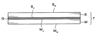
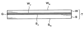
- a processing target wafer W as a processing target substrate and a supporting wafer S as a supporting substrate are bonded via an adhesive G.
- a surface bonded to the support wafer S via the adhesive G is referred to as a “bonding surface W J ” as a surface, and a surface opposite to the bonding surface W J is defined as a “back surface”. It is referred to as “non-bonding surface W N ”.
- a surface bonded to the processing target wafer W via the adhesive G is referred to as a “bonding surface S J ” as a surface, and a surface opposite to the bonding surface S J is defined as a “back surface”. It is referred to as “non-joint surface S N ”.
- the to-be-processed wafer W and the support wafer S are joined, and the superposition
- wafer W is a wafer as a product, for example, joint surface W J A plurality of electronic circuit is formed on the non-bonding surface W N is polished.
- the support wafer S is a wafer having the same diameter as that of the wafer W to be processed and supporting the wafer W to be processed.
- the case where a wafer is used as the support substrate will be described, but another substrate such as a glass substrate may be used.
- the bonding system 1 includes cassettes C W , C S , and C T that can accommodate, for example, a plurality of wafers W to be processed, a plurality of support wafers S, and a plurality of superposed wafers T, respectively.
- the loading / unloading station 2 for loading / unloading and the bonding processing station 3 including various processing apparatuses for performing predetermined processing on the wafer W to be processed, the support wafer S, and the overlapped wafer T are integrally connected. Yes.
- the loading / unloading station 2 is provided with a cassette mounting table 10.
- the cassette mounting table 10 is provided with a plurality of, for example, four cassette mounting plates 11.
- the cassette mounting plates 11 are arranged in a line in the X direction (vertical direction in FIG. 1). These cassette mounting plates 11, cassettes C W to the outside of the interface system 1, C S, when loading and unloading the C T, a cassette C W, C S, can be placed on C T .
- the carry-in / out station 2 is configured to be capable of holding a plurality of wafers W to be processed, a plurality of support wafers S, and a plurality of superposed wafers T.
- the number of cassette mounting plates 11 is not limited to the present embodiment, and can be arbitrarily determined.
- One of the cassettes may be used for collecting defective wafers. That is, this is a cassette that can separate from a normal superposed wafer T a wafer in which a defect occurs in the joining of the processing target wafer W and the supporting wafer S due to various factors.
- this is a cassette that can separate from a normal superposed wafer T a wafer in which a defect occurs in the joining of the processing target wafer W and the supporting wafer S due to various factors.
- using a one cassette C T for the recovery of the fault wafer, and using the other cassette C T for the accommodation of a normal bonded wafer T among the plurality of cassettes C T, using a one cassette C T for the recovery of the fault wafer, and using the other cassette C T for the accommodation of a normal bonded wafer T.
- a wafer transfer unit 20 is provided adjacent to the cassette mounting table 10.
- the wafer transfer unit 20 is provided with a wafer transfer device 22 that is movable on a transfer path 21 extending in the X direction.
- the wafer transfer device 22 is also movable in the vertical direction and around the vertical axis ( ⁇ direction), and the cassettes C W , C S , and C T on each cassette mounting plate 11 and the first of the bonding processing station 3 to be described later.
- the wafer to be processed W, the support wafer S, and the overlapped wafer T can be transferred between the transition devices 50 and 51 of the third processing block G3.
- the bonding processing station 3 is provided with a plurality of, for example, three processing blocks G1, G2, and G3 provided with various processing apparatuses.
- the first processing block G1 is provided on the front side of the bonding processing station 3 (X direction negative direction side in FIG. 1), and the back side of the bonding processing station 3 (X direction positive direction side in FIG. 1). Is provided with a second processing block G2.
- a third processing block G3 is provided on the side of the loading / unloading station 2 of the bonding processing station 3 (the Y direction negative direction side in FIG. 1).
- bonding devices 30 to 33 for pressing and bonding the processing target wafer W and the supporting wafer S via the adhesive G are provided in this order from the loading / unloading station 2 side in the Y direction. They are arranged side by side.
- the coating apparatus 40 that applies the adhesive G to the wafer W to be processed and the wafer W to which the adhesive G is applied are heated to a predetermined temperature.
- Heat treatment apparatuses 41 to 43 and similar heat treatment apparatuses 44 to 46 are arranged in this order in the direction toward the loading / unloading station 2 (the negative direction in the Y direction in FIG. 1).
- the heat treatment apparatuses 41 to 43 and the heat treatment apparatuses 44 to 46 are provided in three stages in this order from the bottom.
- the number of the heat treatment apparatuses 41 to 46 and the arrangement in the vertical direction and the horizontal direction can be arbitrarily set.
- transition devices 50 and 51 for the processing target wafer W, the supporting wafer S, and the superposed wafer T are provided in two stages in this order from the bottom.
- a wafer transfer region 60 is formed in a region surrounded by the first processing block G1 to the third processing block G3.
- a wafer transfer device 61 is disposed in the wafer transfer region 60. Note that the pressure in the wafer transfer region 60 is equal to or higher than atmospheric pressure, and the wafer to be processed W, the support wafer S, and the superposed wafer T are transferred in a so-called atmospheric system in the wafer transfer region 60.
- the wafer transfer device 61 has, for example, a transfer arm that can move around the vertical direction, horizontal direction (Y direction, X direction), and vertical axis.
- the wafer transfer device 61 moves within the wafer transfer region 60, and moves to a predetermined device in the surrounding first processing block G1, second processing block G2, and third processing block G3. S and superposed wafer T can be conveyed.
- the bonding apparatus 30 includes a processing container 100 that can seal the inside.
- a loading / unloading port 101 for the wafer W to be processed, the support wafer S, and the overlapped wafer T is formed on the side surface of the processing container 100 on the wafer transfer region 60 side, and an opening / closing shutter (not shown) is provided at the loading / unloading port. Yes.
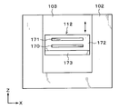
- the inside of the processing container 100 is partitioned by the inner wall 102 into a preprocessing region D1 and a joining region D2.
- the loading / unloading port 101 described above is formed on the side surface of the processing container 100 in the preprocessing region D1.
- a carry-in / out port 103 for the wafer W to be processed, the support wafer S, and the overlapped wafer T is also formed on the inner wall 102.
- a delivery unit 110 for delivering the wafer W to be processed, the support wafer S, and the overlapped wafer T to and from the outside of the bonding apparatus 30 is provided.
- the delivery unit 110 is disposed adjacent to the loading / unloading port 101.
- a plurality of, for example, two stages of delivery units 110 are arranged in the vertical direction, and any two of the processing target wafer W, the supporting wafer S, and the overlapped wafer T can be delivered at the same time.
- the processing target wafer W or the support wafer S before bonding may be delivered by one delivery unit 110, and the superposed wafer T after joining may be delivered by another delivery unit 110.
- the wafer W to be processed before bonding may be delivered by one delivery unit 110 and the support wafer S before joining may be delivered by another delivery unit 110.
- a reversing unit 111 for reversing the front and back surfaces of the support wafer S is provided on the Y direction negative direction side of the pretreatment region D1, that is, on the loading / unloading port 103 side, vertically above the delivery unit 110. Note that the reversing unit 111 can adjust the horizontal direction of the support wafer S as described later, and can also adjust the horizontal direction of the wafer W to be processed.
- a transfer unit 112 that transfers the wafer W, the support wafer S, and the overlapped wafer T to the delivery unit 110, the reversing unit 111, and the bonding unit 113 described later is provided. ing.
- the transport unit 112 is attached to the loading / unloading port 103.
- a bonding portion 113 that presses and bonds the processing target wafer W and the support wafer S via the adhesive G is provided.
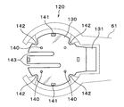
- the delivery unit 110 includes a delivery arm 120 and wafer support pins 121.
- the delivery arm 120 can deliver the wafer W to be processed, the support wafer S, and the overlapped wafer T to the outside of the bonding apparatus 30, that is, between the wafer transfer device 61 and the wafer support pins 121.
- the wafer support pins 121 are provided in a plurality of, for example, three locations, and can support the processing target wafer W, the supporting wafer S, and the overlapped wafer T.
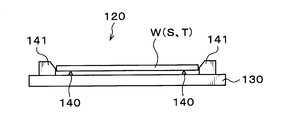
- the delivery arm 120 includes an arm unit 130 that holds the processing target wafer W, the support wafer S, and the overlapped wafer T, and an arm driving unit 131 that includes, for example, a motor.
- the arm part 130 has a substantially disk shape.
- the arm drive unit 131 can move the arm unit 130 in the X direction (vertical direction in FIG. 5).
- the arm drive part 131 is attached to the rail 132 extended
- the delivery arm 120 can move in the horizontal direction (X direction and Y direction), and the wafer W to be processed, the support wafer S, and the overlap between the wafer transfer device 61 and the wafer support pins 121.
- the wafer T can be delivered smoothly.
- a plurality of, for example, four wafer support pins 140 for supporting the processing target wafer W, the supporting wafer S, and the overlapped wafer T are provided on the arm unit 130.
- a guide 141 for positioning the processing target wafer W, the supporting wafer S, and the overlapped wafer T supported by the wafer supporting pins 140 is provided on the arm unit 130.
- a plurality of guides 141 are provided, for example, at four locations so as to guide the side surfaces of the processing target wafer W, the supporting wafer S, and the overlapped wafer T.
- notches 142 are formed at, for example, four locations on the outer periphery of the arm portion 130.
- the notch 142 causes the transfer arm of the wafer transfer device 61 to interfere with the arm unit 130 when the wafer W to be processed, the support wafer S, and the overlapped wafer T are transferred from the transfer arm of the wafer transfer device 61 to the transfer arm 120. Can be prevented.
- the arm part 130 is formed with two slits 143 along the X direction.
- the slit 143 is formed from the end surface of the arm portion 130 on the wafer support pin 121 side to the vicinity of the center portion of the arm portion 130.
- the slit 143 can prevent the arm unit 130 from interfering with the wafer support pins 121.
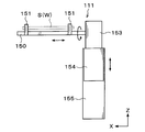
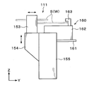
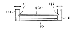
- the reversing unit 111 has a holding arm 150 that holds the support wafer S and the wafer W to be processed, as shown in FIGS.
- the holding arm 150 extends in the horizontal direction (X direction in FIGS. 8 and 9).
- the holding arm 150 is provided with holding members 151 as other holding members that hold the support wafer S and the wafer W to be processed, for example, at four locations.
- the holding member 151 is configured to be movable in the horizontal direction with respect to the holding arm 150.
- a notch 152 for holding the outer periphery of the support wafer S and the wafer W to be processed is formed. These holding members 151 can sandwich and hold the support wafer S and the wafer W to be processed.
- the holding arm 150 is supported by a first drive unit 153 provided with, for example, a motor as shown in FIGS.
- a first drive unit 153 By this first drive unit 153, the holding arm 150 is rotatable about the horizontal axis and can move in the horizontal direction (X direction in FIGS. 8 and 9 and Y direction in FIGS. 8 and 10).
- the first drive unit 153 may rotate the holding arm 150 about the vertical axis to move the holding arm 150 in the horizontal direction.
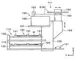
- a second drive unit 154 including a motor or the like is provided below the first drive unit 153.
- the first driving unit 153 can move in the vertical direction along the support pillar 155 extending in the vertical direction.
- the support wafer S and the wafer W to be processed held by the holding member 151 by the first drive unit 153 and the second drive unit 154 can rotate around the horizontal axis and move in the vertical and horizontal directions. it can.
- the first drive unit 153 and the second drive unit 154 constitute a moving mechanism of the present invention.
- the position adjusting mechanism 160 that adjusts the horizontal direction of the support wafer S and the wafer W to be processed held by the holding member 151 is supported by the support column 155 via the support plate 161.
- the position adjustment mechanism 160 is provided adjacent to the holding arm 150.
- the position adjustment mechanism 160 includes a base 162 and a detection unit 163 that detects the positions of the notch portions of the support wafer S and the wafer W to be processed.
- the position adjusting mechanism 160 detects the positions of the notch portions of the support wafer S and the wafer W to be processed by the detection unit 163 while moving the support wafer S and the wafer W to be processed held in the holding member 151 in the horizontal direction.
- the horizontal orientation of the support wafer S and the wafer W to be processed is adjusted by adjusting the position of the notch portion.
- the delivery unit 110 configured as described above is arranged in two stages in the vertical direction, and the reversing unit 111 is arranged vertically above these delivery units 110. That is, the delivery arm 120 of the delivery unit 110 moves in the horizontal direction below the holding arm 150 and the position adjustment mechanism 160 of the reversing unit 111. Further, the wafer support pins 121 of the delivery unit 110 are disposed below the holding arm 150 of the reversing unit 111.
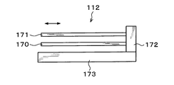
- the transport unit 112 has a plurality of, for example, two transport arms 170 and 171.
- the first transfer arm 170 and the second transfer arm 171 are arranged in two stages in this order from the bottom in the vertical direction.
- the first transfer arm 170 and the second transfer arm 171 have different shapes as will be described later.
- an arm driving unit 172 provided with a motor or the like is provided at the base ends of the transfer arms 170 and 171.
- the arm driving unit 172 allows the transfer arms 170 and 171 to move independently in the horizontal direction.
- the transfer arms 170 and 171 and the arm driving unit 172 are supported by the base 173.
- the transport unit 112 is provided at the loading / unloading port 103 formed on the inner wall 102 of the processing container 100 as shown in FIGS. 4 and 14.
- the transport unit 112 can be moved in the vertical direction along the loading / unloading port 103 by, for example, a driving unit (not shown) provided with a motor or the like.
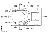
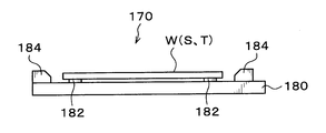
- the first transfer arm 170 holds and transfers the back surface of the processing target wafer W, the supporting wafer S, and the overlapped wafer T (non-bonding surfaces W N and S N in the processing target wafer W and the supporting wafer S). As shown in FIG. 15, the first transfer arm 170 has an arm portion 180 whose tip is branched into two tip portions 180 a and 180 a, and a support that is formed integrally with the arm portion 180 and supports the arm portion 180. Part 181.
- a plurality of resin O-rings 182 as first holding members are provided, for example, at four locations.
- the O-ring 182 comes into contact with the back surface of the wafer to be processed W, the support wafer S, and the overlapped wafer T, and the frictional force between the O-ring 182 and the back surface of the wafer to be processed W, the support wafer S, and the overlap wafer T is
- the O-ring 182 holds the back surface of the processing target wafer W, the supporting wafer S, and the overlapped wafer T.
- the first transfer arm 170 can horizontally hold the processing target wafer W, the supporting wafer S, and the superposed wafer T on the O-ring 182.
- guide members 183 and 184 provided on the outside of the processing target wafer W, the support wafer S, and the superposed wafer T held by the O-ring 182 are provided.
- the first guide member 183 is provided at the distal end of the distal end portion 180 a of the arm portion 180.
- the second guide member 184 is formed in an arc shape along the outer periphery of the processing target wafer W, the supporting wafer S, and the overlapped wafer T, and is provided on the supporting portion 181 side. These guide members 183 and 184 can prevent the wafer W to be processed, the support wafer S, and the overlapped wafer T from jumping out of the first transfer arm 170 or sliding down.
- the to-be-processed wafer W, the support wafer S, and the overlapped wafer T are held at appropriate positions on the O-ring 182, the to-be-processed wafer W, the support wafer S, and the overlapped wafer T are in contact with the guide members 183 and 184. do not do.
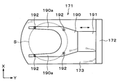
- Second transfer arm 171 carries for example the surface of the support wafer S, that is, holding the outer periphery of the joint surface S J. That is, the second transfer arm 171 holds and conveys the outer periphery of the joint surface S J of the support wafer S to the front and back surfaces by the reversing unit 111 has been reversed. As shown in FIG. 17, the second transfer arm 171 has an arm portion 190 whose front end branches into two front end portions 190 a and 190 a, and a support that is formed integrally with the arm portion 190 and supports the arm portion 190. Part 191.
- the 2nd holding member 192 is provided in multiple, for example, four places.
- the second holding member 192 includes a mounting portion 193 for mounting the outer peripheral portion of the joint surface S J of the support wafer S, extending from the mounting portion 193 upwards, the inner surface from the lower side to the upper side And a taper portion 194 expanding in a taper shape.
- the mounting portion 193 holds an outer peripheral portion within 1 mm from the peripheral edge of the support wafer S, for example.
- the support wafer S delivered to the second holding member 192 is displaced from a predetermined position in the horizontal direction.
- the support wafer S is smoothly guided and positioned by the taper portion 194 and is held by the placement portion 193.
- the second transfer arm 171 can hold the support wafer S horizontally on the second holding member 192.
- the notch 201a is formed in the 2nd holding
- the second holding member 192 of the second transfer arm 171 is connected to the second holding unit 201. Interference can be prevented.
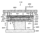
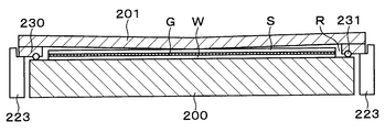
- the bonding unit 113 includes a first holding unit 200 that holds and holds the processing target wafer W on the upper surface, and a second holding unit 201 that holds the supporting wafer S on the lower surface by suction. is doing.
- the first holding unit 200 is provided below the second holding unit 201 and is disposed so as to face the second holding unit 201. That is, the wafer W to be processed held by the first holding unit 200 and the support wafer S held by the second holding unit 201 are arranged to face each other.
- a suction tube 210 for sucking and holding the processing target wafer W is provided inside the first holding unit 200.
- the suction pipe 210 is connected to a negative pressure generator (not shown) such as a vacuum pump.
- the first holding unit 200 is made of a material having a strength that does not deform even when a load is applied by a pressurizing mechanism 260 described later, for example, a ceramic such as silicon carbide ceramic or aluminum nitride ceramic.
- a heating mechanism 211 for heating the processing target wafer W is provided inside the first holding unit 200.
- a heater is used for the heating mechanism 211.
- the moving mechanism 220 that moves the first holding unit 200 and the wafer W to be processed in the vertical direction and the horizontal direction is provided below the first holding unit 200.
- the moving mechanism 220 can move the first holding unit 200 three-dimensionally with an accuracy of, for example, ⁇ 1 ⁇ m.
- the moving mechanism 220 includes a vertical moving unit 221 that moves the first holding unit 200 in the vertical direction and a horizontal moving unit 222 that moves the first holding unit 200 in the horizontal direction.
- the vertical moving unit 221 and the horizontal moving unit 222 each have, for example, a ball screw (not shown) and a motor (not shown) that rotates the ball screw.
- a support member 223 that is extendable in the vertical direction is provided.
- the support member 223 is provided at, for example, three locations outside the first holding unit 200. As shown in FIG. 21, the support member 223 can support the protruding portion 230 provided to protrude downward from the lower surface of the outer periphery of the second holding portion 201.
- the wafer W to be processed on the first holding unit 200 can be aligned in the horizontal direction, and the first holding unit 200 is raised as shown in FIG.
- a bonding space R for bonding the processing wafer W and the support wafer S can be formed.
- the joint space R is a space surrounded by the first holding part 200, the second holding part 201, and the protruding part 230. Further, when the bonding space R is formed, the vertical distance between the processing target wafer W and the supporting wafer S in the bonding space R can be adjusted by adjusting the height of the support member 223.
- lifting pins are provided below the first holding unit 200 for supporting and lifting the wafer to be processed W or the overlapped wafer T from below.
- the elevating pin is inserted through a through hole (not shown) formed in the first holding part 200 and can protrude from the upper surface of the first holding part 200.
- the above-described protruding portion 230 that protrudes downward from the outer peripheral lower surface is formed on the outer peripheral lower surface of the second holding portion 201.
- the protruding portion 230 is formed along the outer periphery of the second holding portion 201. Note that the protruding portion 230 may be formed integrally with the second holding portion 201.
- a sealing material 231 for maintaining the airtightness of the joining space R is provided on the lower surface of the protruding portion 230.
- the sealing material 231 is provided in an annular shape in a groove formed on the lower surface of the protruding portion 230, and for example, an O-ring is used. Moreover, the sealing material 231 has elasticity. Note that the sealing material 231 may be any component having a sealing function, and is not limited to this embodiment.
- a suction tube 240 for sucking and holding the support wafer S is provided inside the second holding unit 201.
- the suction tube 240 is connected to a negative pressure generator (not shown) such as a vacuum pump.
- an intake pipe 241 for taking in the atmosphere of the joint space R is provided inside the second holding unit 201.
- One end of the intake pipe 241 opens at a place where the support wafer S is not held on the lower surface of the second holding unit 201.
- the other end of the intake pipe 241 is connected to a negative pressure generator (not shown) such as a vacuum pump.
- a heating mechanism 242 for heating the support wafer S is provided inside the second holding unit 201.
- a heater is used for the heating mechanism 242.
- the pressurizing mechanism 260 includes a pressure vessel 261 provided so as to cover the processing target wafer W and the support wafer S, and a fluid supply pipe 262 that supplies a fluid, for example, compressed air, to the inside of the pressure vessel 261.
- the support member 250 is configured to be extendable in the vertical direction, and is provided at, for example, three locations outside the pressure vessel 261.
- the pressure vessel 261 is made of, for example, a bellows made of, for example, stainless steel that can expand and contract in the vertical direction.
- the lower surface of the pressure vessel 261 is in contact with the upper surface of the second holding unit 201, and the upper surface is in contact with the lower surface of the support plate 263 provided above the second holding unit 201.
- the fluid supply pipe 262 has one end connected to the pressure vessel 261 and the other end connected to a fluid supply source (not shown). Then, by supplying fluid from the fluid supply pipe 262 to the pressure vessel 261, the pressure vessel 261 extends.
- the pressure vessel 261 extends only in the downward direction, and the second holding portion 201 provided on the lower surface of the pressure vessel 261 is moved downward. Can be pressed.
- the pressure vessel 261 can press the second holding part 201 uniformly in the surface. Adjustment of the load when pressing the second holding unit 201 is performed by adjusting the pressure of the compressed air supplied to the pressure vessel 261.
- the support plate 263 is preferably formed of a member having a strength that does not deform even when the pressure mechanism 260 receives a reaction force of a load applied to the second holding unit 201. Note that the support plate 263 of this embodiment may be omitted, and the upper surface of the pressure vessel 261 may be in contact with the ceiling surface of the processing vessel 100.
- the configuration of the joining devices 31 to 33 is the same as the configuration of the joining device 30 described above, and a description thereof will be omitted.
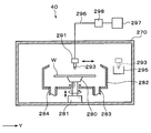
- the coating device 40 has a processing container 270 that can be sealed inside.
- a loading / unloading port (not shown) for the wafer W to be processed is formed on the side surface of the processing container 270 on the wafer transfer region 60 side, and an opening / closing shutter (not shown) is provided at the loading / unloading port.
- a spin chuck 280 that holds and rotates the wafer W to be processed is provided at the center of the processing container 270.
- the spin chuck 280 has a horizontal upper surface, and a suction port (not shown) for sucking the wafer W to be processed is provided on the upper surface, for example.
- the wafer W to be processed can be sucked and held on the spin chuck 280 by suction from the suction port.
- a chuck drive unit 281 provided with a motor or the like is provided below the spin chuck 280.
- the spin chuck 280 can be rotated at a predetermined speed by the chuck driving unit 281.
- the chuck driving unit 281 is provided with an elevating drive source (not shown) such as a cylinder, and the spin chuck 280 can be moved up and down.
- a cup 282 that receives and collects the liquid scattered or dropped from the wafer W to be processed.
- a discharge pipe 283 for discharging the collected liquid
- an exhaust pipe 284 for evacuating and exhausting the atmosphere in the cup 282.
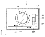
- a rail 290 extending along the Y direction (left-right direction in FIG. 23) is formed on the X direction negative direction (downward direction in FIG. 23) side of the cup 282.
- the rail 290 is formed, for example, from the outside of the cup 282 on the Y direction negative direction (left direction in FIG. 23) side to the outside of the Y direction positive direction (right direction in FIG. 23) side.
- An arm 291 is attached to the rail 290.
- An adhesive nozzle 293 that supplies a liquid adhesive G to the wafer W to be processed is supported on the arm 291 as shown in FIGS.
- the arm 291 is movable on the rail 290 by a nozzle driving unit 294 shown in FIG.
- the adhesive nozzle 293 can move from the standby unit 295 installed on the outer side of the cup 282 on the positive side in the Y direction to above the center of the wafer W to be processed in the cup 282, and further to the wafer W to be processed. It can move in the radial direction of the wafer W to be processed.
- the arm 291 can be moved up and down by a nozzle driving unit 294, and the height of the adhesive nozzle 293 can be adjusted.
- a supply pipe 296 for supplying the adhesive G to the adhesive nozzle 293 is connected to the adhesive nozzle 293 as shown in FIG.
- the supply pipe 296 communicates with an adhesive supply source 297 that stores the adhesive G therein.
- the supply pipe 296 is provided with a supply device group 298 including a valve for controlling the flow of the adhesive G, a flow rate adjusting unit, and the like.
- a back rinse nozzle (not shown) for injecting the cleaning liquid toward the back surface of the processing target wafer W, that is, the non-bonding surface W N may be provided below the spin chuck 280.
- the non-bonded surface W N of the wafer to be processed W and the outer peripheral portion of the wafer to be processed W are cleaned by the cleaning liquid sprayed from the back rinse nozzle.
- the heat treatment apparatus 41 has a processing container 300 that can be closed.
- a loading / unloading port (not shown) for the wafer W to be processed is formed on the side surface of the processing container 300 on the wafer transfer region 60 side, and an opening / closing shutter (not shown) is provided at the loading / unloading port.
- a gas supply port 301 for supplying an inert gas such as nitrogen gas is formed inside the processing container 300 on the ceiling surface of the processing container 300.
- a gas supply pipe 303 communicating with a gas supply source 302 is connected to the gas supply port 301.
- the gas supply pipe 303 is provided with a supply device group 304 including a valve for controlling the flow of the inert gas, a flow rate adjusting unit, and the like.
- a suction port 305 for sucking the atmosphere inside the processing container 300 is formed on the bottom surface of the processing container 300.
- An intake pipe 307 communicating with a negative pressure generator 306 such as a vacuum pump is connected to the intake port 305.
- a heating unit 310 that heat-processes the processing target wafer W and a temperature control unit 311 that controls the temperature of the processing target wafer W are provided.
- the heating unit 310 and the temperature adjustment unit 311 are arranged side by side in the Y direction.
- the heating unit 310 includes an annular holding member 321 that houses the hot plate 320 and holds the outer periphery of the hot plate 320, and a substantially cylindrical support ring 322 that surrounds the outer periphery of the holding member 321.
- the hot plate 320 has a thick, substantially disk shape, and can place and heat the wafer W to be processed.
- the heating plate 320 includes a heater 323, for example.
- the heating temperature of the hot plate 320 is controlled by, for example, the control unit 360 (see FIG. 1), and the processing target wafer W placed on the hot plate 320 is heated to a predetermined temperature.
- the elevating pin 330 can be moved up and down by the elevating drive unit 331. Near the center of the hot plate 320, through holes 332 that penetrate the hot plate 320 in the thickness direction are formed, for example, at three locations. The elevating pins 330 are inserted through the through holes 332 and can protrude from the upper surface of the heat plate 320.
- the temperature adjustment unit 311 has a temperature adjustment plate 340.
- the temperature adjustment plate 340 has a substantially rectangular flat plate shape, and the end surface on the heat plate 320 side is curved in an arc shape.
- two slits 341 along the Y direction are formed in the temperature adjustment plate 340.
- the slit 341 is formed from the end surface of the temperature adjustment plate 340 on the heat plate 320 side to the vicinity of the center of the temperature adjustment plate 340.
- the slits 341 can prevent the temperature adjustment plate 340 from interfering with the elevating pins 330 of the heating unit 310 and elevating pins 350 of the temperature adjusting unit 311 described later.
- the temperature adjustment plate 340 includes a temperature adjustment member (not shown) such as a Peltier element.
- the cooling temperature of the temperature adjustment plate 340 is controlled by, for example, the control unit 360 (see FIG. 1), and the wafer W to be processed placed on the temperature adjustment plate 340 is cooled to a predetermined temperature.
- the temperature adjustment plate 340 is supported by the support arm 342 as shown in FIG.
- a drive unit 343 is attached to the support arm 342.
- the drive unit 343 is attached to a rail 344 extending in the Y direction.
- the rail 344 extends from the temperature adjustment unit 311 to the heating unit 310.
- the drive unit 343 allows the temperature adjustment plate 340 to move between the heating unit 310 and the temperature adjustment unit 311 along the rail 344.
- the elevating pin 350 can be moved up and down by an elevating drive unit 351.
- the elevating pin 350 is inserted through the slit 341 and can protrude from the upper surface of the temperature adjusting plate 340.
- the configuration of the heat treatment apparatuses 42 to 46 is the same as that of the heat treatment apparatus 41 described above, and a description thereof will be omitted.
- the control unit 360 is a computer, for example, and has a program storage unit (not shown).
- the program storage unit stores a program for controlling processing of the processing target wafer W, the supporting wafer S, and the overlapped wafer T in the bonding system 1.
- the program storage unit also stores a program for controlling the operation of drive systems such as the above-described various processing apparatuses and transfer apparatuses to realize the below-described joining process in the joining system 1.
- the program is recorded on a computer-readable storage medium H such as a computer-readable hard disk (HD), a flexible disk (FD), a compact disk (CD), a magnetic optical desk (MO), or a memory card. May have been installed in the control unit 360 from the storage medium H.
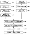
- FIG. 27 is a flowchart showing an example of main steps of the joining process.
- a cassette C W housing a plurality of the processed the wafer W, the cassette C S accommodating a plurality of support wafer S, and an empty cassette C T is a predetermined cassette mounting plate 11 of the carry-out station 2 Placed.
- the wafer W to be processed in the cassette CW is taken out by the wafer transfer device 22 and transferred to the transition device 50 of the third processing block G3 of the bonding processing station 3.
- the wafer W to be processed is transported with its non-bonding surface W N facing downward.
- the wafer W to be processed is transferred to the coating device 40 by the wafer transfer device 61.
- the wafer W to be processed loaded into the coating device 40 is transferred from the wafer transfer device 61 to the spin chuck 280 and is sucked and held. At this time, the non-bonding surface W N of the wafer W is held by suction.
- the adhesive nozzle 293 of the standby unit 295 is moved above the central portion of the wafer W to be processed by the arm 291. Thereafter, while rotating the wafer W by the spin chuck 280, and supplies the adhesive G from the adhesive nozzles 293 on the bonding surface W J of wafer W. Supplied adhesive G is diffused into the entire surface of the bonding surface W J of wafer W by the centrifugal force, the adhesive G on the bonding surface W J of the wafer W is applied (step of FIG. 27 A1 ).
- the wafer W to be processed is transferred to the heat treatment apparatus 41 by the wafer transfer apparatus 61.
- the inside of the heat treatment apparatus 41 is maintained in the main region of the inert gas.
- the superposed wafer T is transferred from the wafer transfer apparatus 61 to the lift pins 350 that have been lifted and waited in advance. Subsequently, the elevating pins 350 are lowered, and the processing target wafer W is placed on the temperature adjustment plate 340.
- the temperature adjustment plate 340 is moved along the rail 344 to the upper side of the heat plate 320 by the driving unit 343, and the wafer W to be processed is transferred to the lift pins 330 that have been lifted and waited in advance. Thereafter, the elevating pins 330 are lowered, and the wafer W to be processed is placed on the hot plate 320. Then, the wafer W to be processed on the hot plate 320 is heated to a predetermined temperature, for example, 100 ° C. to 250 ° C. (step A2 in FIG. 27). By performing the heating by the hot plate 320, the adhesive G on the wafer W to be processed is heated and the adhesive G is cured.
- a predetermined temperature for example, 100 ° C. to 250 ° C.
- the elevating pin 330 is raised, and the temperature adjusting plate 340 is moved above the hot plate 320.
- the wafer W to be processed is transferred from the lift pins 330 to the temperature adjustment plate 340, and the temperature adjustment plate 340 moves to the wafer transfer region 60 side.
- the temperature of the processing target wafer W is adjusted to a predetermined temperature.
- the wafer W to be processed that has been heat-treated by the heat treatment apparatus 41 is transferred to the bonding apparatus 30 by the wafer transfer apparatus 61.
- the wafer W to be processed transferred to the bonding apparatus 30 is transferred from the wafer transfer apparatus 61 to the transfer arm 120 of the transfer unit 110 and then transferred from the transfer arm 120 to the wafer support pins 121. Thereafter, the wafer W to be processed is transferred from the wafer support pins 121 to the reversing unit 111 by the first transfer arm 170 of the transfer unit 112.
- the wafer W to be processed transferred to the reversing unit 111 is held by the holding member 151 and moved to the position adjusting mechanism 160. Then, the position adjusting mechanism 160 adjusts the position of the notch portion of the processing target wafer W to adjust the horizontal direction of the processing target wafer W (step A3 in FIG. 27).
- the wafer W to be processed is transferred from the reversing unit 111 to the bonding unit 113 by the first transfer arm 170 of the transfer unit 112.
- the to-be-processed wafer W conveyed to the junction part 113 is mounted in the 1st holding
- the supporting wafer S is processed following the processing target wafer W.
- the support wafer S is transferred to the bonding apparatus 30 by the wafer transfer device 61.
- description is abbreviate
- the support wafer S transferred to the bonding apparatus 30 is transferred from the wafer transfer apparatus 61 to the transfer arm 120 of the transfer unit 110 and then transferred from the transfer arm 120 to the wafer support pins 121. Thereafter, the support wafer S is transferred from the wafer support pins 121 to the reversing unit 111 by the first transfer arm 170 of the transfer unit 112.
- the support wafer S transferred to the reversing unit 111 is held by the holding member 151 and moved to the position adjusting mechanism 160. Then, the position adjustment mechanism 160 adjusts the position of the notch portion of the support wafer S to adjust the horizontal direction of the support wafer S (step A5 in FIG. 27).
- the support wafer S whose horizontal direction has been adjusted is moved in the horizontal direction from the position adjustment mechanism 160 and moved upward in the vertical direction, and then the front and back surfaces thereof are reversed (step A6 in FIG. 27). That is, the bonding surface S J of the support wafer S is directed downward.
- the support wafer S is moved downward in the vertical direction, and then transferred from the reversing unit 111 to the bonding unit 113 by the second transfer arm 171 of the transfer unit 112.
- second transfer arm 171 since it holds only the outer peripheral portion of the joint surface S J of the support wafer S, for example, that the joint surface S J is soiled by particles or the like adhering to the second transfer arm 171 There is no.
- the support wafer S transferred to the bonding unit 113 is sucked and held by the second holding unit 201 (step A7 in FIG. 27).
- the supporting wafer S is held in a state where the bonding surfaces S J is directed downward of the support wafer S.
- the bonding apparatus 30 when the processing target wafer W and the support wafer S are held by the first holding unit 200 and the second holding unit 201, respectively, a moving mechanism is provided so that the processing target wafer W faces the support wafer S.
- the horizontal position of the first holding unit 200 is adjusted by 220 (step A8 in FIG. 27).
- the pressure in the pressure vessel 261 of the pressurizing mechanism 260 may be set to atmospheric pressure, or the upper surface of the second holding unit 201 and the pressure vessel 261 may be maintained. A gap may be formed between the two.
- the first holding unit 200 is raised by the moving mechanism 220 and the support member 223 is extended to support the second holding unit 201 on the support member 223.
- the vertical distance between the wafer to be processed W and the support wafer S is adjusted to be a predetermined distance (step A9 in FIG. 27).
- the predetermined distance is such that when the sealant 231 comes into contact with the first holding unit 200 and the center of the second holding unit 201 and the supporting wafer S is bent as described later, the supporting wafer S Is the height at which the central portion of the wafer contacts the wafer W to be processed. In this way, a sealed joint space R is formed between the first holding part 200 and the second holding part 201.
- the atmosphere of the joint space R is sucked from the suction pipe 241.
- the pressure applied to the upper surface of the second holding portion 201 and the bonding space R are applied to the second holding portion 201.
- the center portion of the second holding portion 201 is bent, and the center portion of the support wafer S held by the second holding portion 201 is also bent.
- the atmosphere of the joining space R is further sucked and the inside of the joining space R is depressurized.
- the second holding unit 201 cannot hold the support wafer S
- the support wafer S as shown in FIG. is dropped down
- the bonding surface S J entire support wafer S comes into contact with the bonding surface W J entire treated wafer W.
- the support wafer S sequentially comes into contact with the processing target wafer W from the central portion toward the radially outer side. That is, for example, even when air that can be a void exists in the bonding space R, the air is always present outside the portion where the support wafer S is in contact with the wafer W to be processed. It is possible to escape from between the processing wafer W and the support wafer S. In this way, the processing target wafer W and the support wafer S are bonded by the adhesive G while suppressing the generation of voids (step A10 in FIG. 27).
- the height of the support member 223 is adjusted, and the lower surface of the second holding unit 201 is brought into contact with the non-joint surface SN of the support wafer S.
- the sealing material 231 is elastically deformed, and the first holding unit 200 and the second holding unit 201 are in close contact with each other.
- maintenance part 201 is set to predetermined
- the overlapped wafer T in which the processing target wafer W and the support wafer S are bonded is transferred from the bonding unit 110 to the delivery unit 110 by the first transfer arm 170 of the transfer unit 112.
- the overlapped wafer T transferred to the transfer unit 110 is transferred to the transfer arm 120 via the wafer support pins 121, and further transferred from the transfer arm 120 to the wafer transfer device 61.
- bonded wafer T is transferred to the transition unit 51 by the wafer transfer apparatus 61, as by the wafer transfer apparatus 22 of the subsequent unloading station 2 is transported to the cassette C T of predetermined cassette mounting plate 11. In this way, a series of bonding processing of the processing target wafer W and the supporting wafer S is completed.
- the processing target wafer W is sequentially processed, the adhesive G is applied to the processing target wafer W, and heated to a predetermined temperature. At 30, the front and back surfaces of the support wafer S are reversed. Thereafter, in the bonding apparatus 30, the wafer W to be processed which has been applied with the adhesive G and heated to a predetermined temperature is bonded to the support wafer S whose front and back surfaces are reversed.
- the processing target wafer W and the supporting wafer S can be processed in parallel.
- the bonding apparatus 30 While the wafer to be processed W and the support wafer S are bonded in the bonding apparatus 30, another wafer to be processed W and the support wafer S can be processed in the coating apparatus 40, the heat treatment apparatus 41, and the bonding apparatus 30. Therefore, the wafer W to be processed and the support wafer S can be bonded efficiently, and the throughput of the bonding process can be improved.
- the bonding apparatus of Patent Document 1 when used, it is necessary to reverse the front and back surfaces of the wafer outside the bonding apparatus. In such a case, it is necessary to transfer the wafer to the bonding apparatus after inverting the front and back surfaces of the wafer, so there is room for improvement in the throughput of the entire bonding process. Further, when the front and back surfaces of the wafer are reversed, the bonded surface of the wafer faces downward. In such a case, when a transfer device that holds the back surface of a normal wafer is used, the bonding surface of the wafer is held by the transfer device. For example, when particles are attached to the transfer device, There was a risk of adhering to the bonding surface of the wafer. Further, the bonding apparatus of Patent Document 1 does not have a function of adjusting the horizontal direction of the wafer and the support substrate, and there is a possibility that the wafer and the support substrate are bonded to each other while being displaced.
- the support wafer S is reversed by the transfer unit 112 after the support wafer S is reversed. Immediately it can be conveyed to the joint 113.
- the reversal of the support wafer S and the bonding of the wafer to be processed W and the support wafer S are performed together in one bonding apparatus 30, the wafer to be processed W and the support wafer S are bonded efficiently. be able to. Therefore, the throughput of the bonding process can be further improved.
- second transfer arm 171 of the transfer unit 112 so holding the outer peripheral portion of the joint surface S J of the support wafer S, for example, that the joint surface S J is soiled by particles or the like adhering to the second transfer arm 171 There is no.
- the first transfer arm 170 of the transfer unit 112 holds and transfers the non-bonded surface W N of the processing target wafer W, the bonded surface S J of the support wafer S, and the back surface of the overlapped wafer T.
- the transfer unit 112 since the transfer unit 112 includes the two types of transfer arms 170 and 171, the wafer to be processed W, the support wafer S, and the overlapped wafer T can be transferred efficiently.
- the taper portion 194 of the second holding member 192 is transferred to, for example, the second holding member 192. Even if the support wafer S to be moved is displaced from a predetermined position in the horizontal direction, the support wafer S can be smoothly guided and positioned by the tapered portion 194.
- first transfer arm 170 guide members 183 and 184 are provided on the arm unit 180, so that the wafer W to be processed, the support wafer S, and the overlapped wafer T jump out of the first transfer arm 170. , Can prevent sliding down.
- the reversing unit 720 can reverse the front and back surfaces of the supporting wafer S by the first driving unit 153 and can adjust the horizontal direction of the supporting wafer S and the wafer W to be processed by the position adjusting mechanism 160. Therefore, the support wafer S and the processing target wafer W can be appropriately bonded at the bonding portion 113. Further, in the bonding portion 113, the one reversing portion 111 performs both the reversal of the support wafer S and the adjustment of the horizontal orientation of the support wafer S and the wafer W to be processed. The wafer S can be joined efficiently. Therefore, the throughput of the bonding process can be further improved.
- the delivery unit 110 is arranged in two stages in the vertical direction, any two of the processing target wafer W, the supporting wafer S, and the superposed wafer T can be delivered at the same time. Therefore, the wafer W to be processed, the support wafer S, and the superposed wafer T can be efficiently transferred to and from the outside of the bonding apparatus 30, and the throughput of the bonding process can be further improved.
- the inside of the heat treatment apparatus 41 can be maintained in an inert gas atmosphere, it is possible to suppress the formation of an oxide film on the wafer W to be processed. For this reason, the heat processing of the to-be-processed wafer W can be performed appropriately.
- the pressure in the heat treatment apparatus 41 is negative with respect to the pressure in the wafer transfer region 60. For this reason, when the opening / closing shutter of the processing container of the heat treatment apparatus 41 is opened, an air flow from the wafer transfer region 60 toward the heat treatment apparatus 41 is generated. Therefore, the heated atmosphere in the heat treatment apparatus 41 does not flow into the wafer transfer region 60, and the wafer W, the support wafer S, and the superposed wafer T transferred in the wafer transfer region 60 are appropriately set at a predetermined temperature. Can be transported.
- an inspection device 370 for inspecting the superposed wafer T joined by the joining device 30 may be further provided.
- the inspection device 370 is disposed, for example, on the uppermost layer of the third processing block G3.
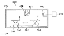
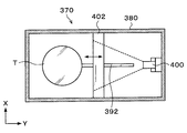
- the inspection apparatus 370 has a processing container 380 as shown in FIG.
- a loading / unloading port (not shown) for loading and unloading the overlapped wafer T is formed on the side surface of the processing container 380 on the wafer transfer region 60 side, and an opening / closing shutter (not shown) is provided at the loading / unloading port.
- a chuck 390 that holds the superposed wafer T by suction is provided as shown in FIG.
- the chuck 390 can be freely rotated and stopped by a chuck driving unit 391 including a motor, for example, and has an alignment function for adjusting the position of the overlapped wafer T.
- a rail 392 extending from one end side (Y direction negative direction side in FIG. 33) to the other end side (Y direction positive direction side in FIG. 33) is provided on the bottom surface of the processing container 380. Yes.
- the chuck drive unit 391 is attached on the rail 392.
- the chuck 390 can be moved along the rail 392 by the chuck driving unit 391 and can be moved up and down.
- the imaging unit 400 is provided on the side surface on the other end side in the processing container 380 (Y direction positive direction side in FIG. 33).
- a wide-angle CCD camera is used for the imaging unit 400.
- a half mirror 401 is provided near the upper center of the processing container 380.
- the half mirror 401 is provided at a position facing the imaging unit 400 and is inclined by 45 degrees from the vertical direction.
- an infrared irradiation unit 402 that irradiates the superposed wafer T with infrared rays is provided, and the half mirror 401 and the infrared irradiation unit 402 are fixed to the upper surface of the processing container 380.
- the infrared irradiation part 402 is extended
- the overlapped wafer T bonded in the process A ⁇ b> 11 in the bonding apparatus 30 described above is transferred to the inspection apparatus 370 by the wafer transfer apparatus 61.
- the overlapped wafer T carried into the inspection device 370 is transferred from the wafer transfer device 61 to the chuck 390.
- the chuck 390 is moved along the rail 392 by the chuck driving unit 391, and infrared light is irradiated from the infrared irradiation unit 402 to the moving superposed wafer T.
- the entire surface of the overlapped wafer T is imaged by the imaging unit 400 via the half mirror 401.
- the captured image of the overlapped wafer T is output to the control unit 360, and the control unit 360 inspects whether or not the overlapped wafer T is appropriately bonded, for example, the presence or absence of voids in the overlapped wafer T. Thereafter, bonded wafer T is transferred to the transition unit 51 by the wafer transfer apparatus 61, as by the wafer transfer apparatus 22 of the subsequent unloading station 2 is transported to the cassette C T of predetermined cassette mounting plate 11.
- the processing conditions in the bonding system 1 can be corrected based on the inspection result. Therefore, the wafer W to be processed and the support wafer S can be bonded more appropriately.
- a temperature adjusting device for cooling the processing target wafer W heat-treated by the heat treatment device 41 to a predetermined temperature may be provided.
- the temperature of the wafer W to be processed is adjusted to an appropriate temperature, so that subsequent processing can be performed more smoothly.
- the wafer to be processed W and the support wafer S are bonded in a state where the wafer to be processed W is disposed on the lower side and the support wafer S is disposed on the upper side.
- the vertical arrangement of the wafer W and the support wafer S may be reversed.
- the above-described steps A5 to A7 are performed on the wafer W to be processed, and the front and back surfaces of the wafer W to be processed are reversed.
- the above-described steps A8 to A11 are performed, and the support wafer S and the wafer W to be processed are bonded.
- the adhesive G is applied to either the processing target wafer W or the support wafer S in the coating apparatus 40, but the adhesive G is applied to both the processing target wafer W and the support wafer S. May be applied.
- the first transfer arm 170 of the transfer unit 112 has the O-ring 182 for holding the processing target wafer W, the support wafer S, and the overlapped wafer T.
- the present invention is not limited to this.
- a frictional force may be generated between the first holding member and the back surface of the processing target wafer W, the supporting wafer S, and the overlapped wafer T. You may have a suction pad etc.
- the conveyance unit 112 may be omitted from the joining device 30.
- the wafer W to be processed and the support wafer S are delivered between the delivery unit 110 and the reversing unit 111, and between the reversing unit 111 and the joining unit 113.
- the processing wafer W and the support wafer S are delivered.
- the transfer unit 112 in addition to the reversal of the processed wafer W and the support wafer S and the adjustment of the horizontal direction in the reversing unit 111, the transfer of the processed wafer W and the support wafer S is performed.
- the throughput of the bonding process is reduced as compared with the above embodiment.
- the apparatus configuration is simplified. Therefore, it is useful to use the bonding apparatus 30 in which the transfer unit 112 is omitted. is there.
- the coating apparatus 40 has one adhesive nozzle 293, but may have, for example, two adhesive nozzles. In this case, it is possible to cope with the case where two types of adhesives are used, and one adhesive can be used for bonding evaluation.
- bonded wafer T joined by bonding system 1 a predetermined process of polishing processing of non-bonding surface W N of the wafer W is performed in the outside of the interface system 1. Thereafter, the overlapped wafer T is peeled off from the processing target wafer W and the supporting wafer S, and the processing target wafer W is commercialized.
- the substrate processing system 410 provided with the bonding system 1 may further include a peeling system 420 that peels the superposed wafer T into the wafer W to be processed and the support wafer S. .
- the peeling system 420 the superposed wafer T bonded with the adhesive G shown in FIG.
- a plurality of electronic circuits are formed as described above on the bonding surface W J of the processing target wafer W.
- the non-bonding surface W N of the wafer W to be processed is polished, and the wafer W to be processed is thinned (for example, the thickness is 50 ⁇ m).
- the peeling system 420 includes cassettes C W , C S , and C T that can accommodate, for example, a plurality of wafers W to be processed, a plurality of support wafers S, and a plurality of superposed wafers T, respectively.
- An interface station 424 that transfers the wafer W to be processed to and from the station 423 is integrally connected.
- the loading / unloading station 421 and the peeling processing station 422 are arranged side by side in the X direction (vertical direction in FIG. 35).
- a wafer transfer region 425 is formed between the carry-in / out station 421 and the peeling processing station 422.
- the interface station 424 is arranged on the negative side in the Y direction (left side in FIG. 35) of the carry-in / out station 421, the peeling processing station 422, and the wafer transfer region 425.
- the loading / unloading station 421 is provided with a cassette mounting table 430.
- the cassette mounting table 430 is provided with a plurality of, for example, three cassette mounting plates 431.
- the cassette mounting plates 431 are arranged in a line in the Y direction (left and right direction in FIG. 35).
- the cassettes C W , C S , and C T can be placed on these cassette mounting plates 431 when the cassettes C W , C S , and C T are carried into and out of the peeling system 420.
- the carry-in / out station 421 is configured to be capable of holding a plurality of wafers W to be processed, a plurality of support wafers S, and a plurality of superposed wafers T.
- the number of cassette placement plates 431 is not limited to the present embodiment, and can be arbitrarily determined.
- a plurality of superposed wafers T carried into the carry-in / out station 421 are inspected in advance, and a superposed wafer T including a normal target wafer W and a superposed wafer T including a defective target wafer W; Has been determined.
- a first transfer device 440 is arranged in the wafer transfer area 425.
- the first transfer device 440 includes a transfer arm that can move around, for example, the vertical direction, the horizontal direction (Y direction, X direction), and the vertical axis.
- the first transfer device 440 can move in the wafer transfer region 425 and transfer the processing target wafer W, the support wafer S, and the overlapped wafer T between the transfer-in / out station 421 and the peeling processing station 422.
- the peeling processing station 422 has a peeling device 450 that peels the superposed wafer T from the wafer W to be processed and the support wafer S.
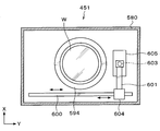
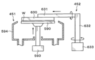
- a first cleaning device 451 for cleaning the wafer to be processed W that has been peeled off is disposed on the negative side in the Y direction of the peeling device 450 (on the left side in FIG. 35).
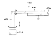
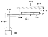
- the 2nd conveying apparatus 452 as another conveying apparatus is provided.
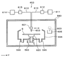
- a second cleaning device 453 for cleaning the peeled support wafer S is disposed on the positive side in the Y direction of the peeling device 450 (right side in FIG. 35).
- the first cleaning device 451, the second transfer device 452, the peeling device 450, and the second cleaning device 453 are arranged in this order from the interface station 424 side in the peeling processing station 422.
- the interface station 424 is provided with a third transfer device 461 as another transfer device that is movable on the transfer path 460 extending in the X direction.
- the third transfer device 461 is also movable in the vertical direction and the vertical axis ( ⁇ direction), and can transfer the wafer W to be processed between the separation processing station 422 and the post-processing station 423.
- a predetermined post-processing is performed on the processing target wafer W peeled off at the peeling processing station 422.
- predetermined post-processing for example, processing for mounting the processing target wafer W, processing for inspecting electrical characteristics of electronic circuits on the processing target wafer W, processing for dicing the processing target wafer W for each chip, and the like are performed. .
- the peeling device 450 has a processing container 500 that can be sealed inside.
- a loading / unloading port (not shown) for the processing target wafer W, the support wafer S, and the overlapped wafer T is formed on the side surface of the processing container 500, and an opening / closing shutter (not shown) is provided at the loading / unloading port.
- a suction port 501 for sucking the atmosphere inside the processing container 500 is formed on the bottom surface of the processing container 500.
- An intake pipe 503 communicating with a negative pressure generator 502 such as a vacuum pump is connected to the intake port 501.
- a first holding unit 510 for sucking and holding the wafer W to be processed on the lower surface and a second holding unit 511 for mounting and holding the support wafer S on the upper surface.
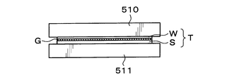
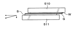
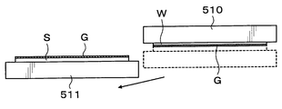
- the first holding unit 510 is provided above the second holding unit 511 and is disposed so as to face the second holding unit 511. That is, in the inside of the processing container 500, the peeling process is performed on the superposed wafer T in a state where the processing target wafer W is disposed on the upper side and the supporting wafer S is disposed on the lower side.
- the first holding unit 510 for example, a porous chuck is used.
- the first holding part 510 has a flat body part 520.
- a porous body 521 is provided on the lower surface side of the main body 520.
- the porous body 521 has, for example, substantially the same diameter as the wafer W to be processed, and is in contact with the non-joint surface W N of the wafer W to be processed.
- silicon carbide is used as the porous body 521.
- a suction space 522 is formed inside the main body 520 and above the porous body 521.
- the suction space 522 is formed so as to cover the porous body 521, for example.
- a suction tube 523 is connected to the suction space 522.
- the suction pipe 523 is connected to a negative pressure generator (not shown) such as a vacuum pump. Then, the non-joint surface W N of the wafer to be processed is sucked from the suction pipe 523 through the suction space 522 and the porous body 521, and the wafer to be processed W is sucked and held by the first holding unit 510.
- a heating mechanism 524 for heating the wafer W to be processed is provided inside the main body 520 and above the suction space 522.
- a heater is used for the heating mechanism 524.
- a support plate 530 that supports the first holding unit is provided on the upper surface of the first holding unit 510.
- the support plate 530 is supported on the ceiling surface of the processing container 500. Note that the support plate 530 of this embodiment may be omitted, and the first holding unit 510 may be supported in contact with the ceiling surface of the processing container 500.
- a suction tube 540 for sucking and holding the support wafer S is provided inside the second holding unit 511.
- the suction pipe 540 is connected to a negative pressure generator (not shown) such as a vacuum pump.
- a heating mechanism 541 for heating the support wafer S is provided inside the second holding unit 511.
- a heater is used for the heating mechanism 541.
- the moving mechanism 550 that moves the second holding unit 511 and the support wafer S in the vertical direction and the horizontal direction is provided below the second holding unit 511.
- the moving mechanism 550 includes a vertical moving unit 551 that moves the second holding unit 511 in the vertical direction and a horizontal moving unit 552 that moves the second holding unit 511 in the horizontal direction.
- the vertical moving unit 551 has a support plate 560 that supports the lower surface of the second holding unit 511, a drive unit 561 that moves the support plate 560 up and down, and a support member 562 that supports the support plate 560.
- the drive unit 561 has, for example, a ball screw (not shown) and a motor (not shown) that rotates the ball screw.
- the support member 562 is configured to be extendable in the vertical direction, and is provided at, for example, three locations between the support plate 560 and a support body 571 described later.
- the horizontal moving unit 552 includes a rail 570 extending along the X direction (left and right direction in FIG. 37), a support 571 attached to the rail 570, and a drive unit 572 that moves the support 571 along the rail 570.
- the drive unit 572 includes, for example, a ball screw (not shown) and a motor (not shown) that rotates the ball screw.
- lift pins (not shown) are provided below the second holding part 511 for supporting the superposed wafer T or the support wafer S from below and moving them up and down.
- the elevating pin is inserted through a through hole (not shown) formed in the second holding part 511 and can protrude from the upper surface of the second holding part 511.
- the first cleaning device 451 has a processing container 580 whose inside can be sealed.
- a loading / unloading port (not shown) for the wafer W to be processed is formed on the side surface of the processing container 580, and an opening / closing shutter (not shown) is provided at the loading / unloading port.
- a porous chuck 590 that holds and rotates the wafer W to be processed is provided at the center of the processing container 580.
- the porous chuck 590 has a flat plate-like main body 591 and a porous body 592 provided on the upper surface side of the main body 591.
- the porous body 592 has, for example, substantially the same diameter as the wafer W to be processed, and is in contact with the non-joint surface W N of the wafer W to be processed.
- silicon carbide is used as the porous body 592.
- a suction pipe (not shown) is connected to the porous body 592, and the non-bonding surface W N of the wafer to be processed W is sucked from the suction pipe through the porous body 592, thereby It can be sucked and held on the porous chuck 590.
- a chuck driving unit 593 provided with a motor or the like is provided below the porous chuck 590.
- the porous chuck 590 can be rotated at a predetermined speed by the chuck driving unit 593.
- the chuck drive unit 593 is provided with an elevating drive source such as a cylinder, for example, and the porous chuck 590 is movable up and down.
- a cup 594 that receives and collects the liquid scattered or dropped from the wafer W to be processed.
- a discharge pipe 595 for discharging the collected liquid
- an exhaust pipe 596 for evacuating and exhausting the atmosphere in the cup 594.
- a rail 600 extending along the Y direction is formed on the negative side of the cup 594 in the X direction (downward direction in FIG. 39).
- the rail 600 is formed, for example, from the outer side of the cup 594 on the Y direction negative direction (left direction in FIG. 39) to the outer side on the Y direction positive direction (right direction in FIG. 39).
- An arm 601 is attached to the rail 600.
- the arm 601 supports a cleaning liquid nozzle 603 for supplying a cleaning liquid, for example, an organic solvent, to the wafer W to be processed.
- the arm 601 is movable on the rail 600 by a nozzle driving unit 604 shown in FIG.
- the cleaning liquid nozzle 603 can move from the standby portion 605 installed outside the positive direction of the Y direction of the cup 594 to above the center of the wafer W to be processed in the cup 594, and further on the wafer W to be processed. Can be moved in the radial direction of the wafer W to be processed.
- the arm 601 can be moved up and down by a nozzle driving unit 604, and the height of the cleaning liquid nozzle 603 can be adjusted.
- a two-fluid nozzle is used as the cleaning liquid nozzle 603.
- a supply pipe 610 for supplying the cleaning liquid to the cleaning liquid nozzle 603 is connected to the cleaning liquid nozzle 603.
- the supply pipe 610 communicates with a cleaning liquid supply source 611 that stores the cleaning liquid therein.
- the supply pipe 610 is provided with a supply device group 612 including a valve for controlling the flow of the cleaning liquid, a flow rate adjusting unit, and the like.
- a supply pipe 613 for supplying an inert gas such as nitrogen gas to the cleaning liquid nozzle 603 is connected to the cleaning liquid nozzle 603.
- the supply pipe 613 communicates with a gas supply source 614 that stores an inert gas therein.
- the supply pipe 613 is provided with a supply device group 615 including a valve for controlling the flow of the inert gas, a flow rate adjusting unit, and the like.
- the cleaning liquid and the inert gas are mixed in the cleaning liquid nozzle 603 and supplied from the cleaning liquid nozzle 603 to the wafer W to be processed.
- a mixture of a cleaning liquid and an inert gas may be simply referred to as “cleaning liquid”.
- lifting pins for supporting the wafer W to be processed from below and lifting it may be provided below the porous chuck 590.
- the elevating pins can pass through a through hole (not shown) formed in the porous chuck 590 and protrude from the upper surface of the porous chuck 590. Then, instead of raising and lowering the porous chuck 590, the raising and lowering pins are raised and lowered, and the wafer W to be processed is transferred to and from the porous chuck 590.
- the configuration of the second cleaning device 453 is substantially the same as the configuration of the first cleaning device 451 described above.
- the second cleaning device 453 is provided with a spin chuck 620 instead of the porous chuck 590 of the first cleaning device 451.
- the spin chuck 620 has a horizontal upper surface, and a suction port (not shown) for sucking, for example, the support wafer S is provided on the upper surface.
- the support wafer S can be sucked and held on the spin chuck 620 by suction from the suction port. Since the other structure of the 2nd washing
- a back rinse nozzle (not shown) for injecting the cleaning liquid toward the back surface of the support wafer S, that is, the non-bonding surface SN is provided below the spin chuck 620. Also good. The non-bonding surface SN of the support wafer S and the outer peripheral portion of the support wafer S are cleaned by the cleaning liquid sprayed from the back rinse nozzle.
- the second transfer device 452 has a Bernoulli chuck 630 that holds the wafer W to be processed.
- the Bernoulli chuck 630 can float the wafer W to be processed by ejecting air, and can hold the wafer W to be sucked and held in a non-contact state.
- Bernoulli chuck 630 is supported by support arm 631.
- the support arm 631 is supported by the first drive unit 632.
- the first drive unit 632 By the first drive unit 632, the support arm 631 is rotatable around the horizontal axis and can be expanded and contracted in the horizontal direction.
- a second drive unit 633 is provided below the first drive unit 632. The second drive unit 633 allows the first drive unit 632 to rotate around the vertical axis and to move up and down in the vertical direction.
- the 3rd conveying apparatus 461 has the structure similar to the 2nd conveying apparatus 452 mentioned above, description is abbreviate
- the second drive unit 633 of the third transport device 461 is attached to the transport path 460 shown in FIG. 35, and the third transport device 461 can move on the transport path 460.
- FIG. 42 is a flowchart showing an example of main steps of the peeling process.
- a cassette C T accommodating a plurality of bonded wafer T, an empty cassette C W, and an empty cassette C S is placed on the predetermined cassette mounting plate 431 of the loading and unloading station 421.
- the superposed wafer T in the cassette CT is taken out by the first transfer device 440 and transferred to the peeling device 450 of the peeling processing station 422.
- the superposed wafer T is transported in a state where the processing target wafer W is disposed on the upper side and the support wafer S is disposed on the lower side.
- the overlapped wafer T carried into the peeling device 450 is sucked and held by the second holding unit 511. Thereafter, the second holding unit 511 is raised by the moving mechanism 550, and the overlapped wafer T is sandwiched and held between the first holding unit 510 and the second holding unit 511 as shown in FIG. At this time, the non-bonding surface W N of the wafer W is held by suction on the first holding portion 510, the non-bonding surface S N of the support wafer S is held by suction to the second holding portion 511.
- the superposed wafer T is heated to a predetermined temperature, for example, 200 ° C. by the heating mechanisms 524 and 541. As a result, the adhesive G in the superposed wafer T is softened.
- the second holding unit 511 and the support wafer S are moved in the vertical direction by the moving mechanism 550 as shown in FIG. And move horizontally, that is, diagonally downward. Then, as shown in FIG. 45, the wafer W to be processed held by the first holding unit 510 and the support wafer S held by the second holding unit 511 are separated (step B1 in FIG. 42).
- the second holding portion 511 moves 100 ⁇ m in the vertical direction and moves 300 mm in the horizontal direction.
- the thickness of the adhesive G in bonded wafer T is a example 30 [mu] m ⁇ 40 [mu] m
- the height of the electronic circuit formed on the bonding surface W J of the processing target wafer W (bump) is For example, 20 ⁇ m. Therefore, the distance between the electronic circuit on the processing target wafer W and the support wafer S is very small. Therefore, for example, when the second holding unit 511 is moved only in the horizontal direction, the electronic circuit and the support wafer S may come into contact with each other, and the electronic circuit may be damaged.
- the second holding portion 511 by moving the second holding portion 511 in the horizontal direction and also in the vertical direction as in the present embodiment, the contact between the electronic circuit and the support wafer S is avoided, and the electronic circuit is damaged. Can be suppressed.
- the ratio of the vertical movement distance and the horizontal movement distance of the second holding unit 511 is set based on the height of the electronic circuit (bump) on the wafer W to be processed.
- the processing target wafer W peeled off by the peeling device 450 is transferred to the first cleaning device 451 by the second transfer device 452.
- a transfer method of the wafer W to be processed by the second transfer device 452 will be described.
- the support arm 631 is extended to place the Bernoulli chuck 630 below the wafer W to be processed held by the first holding unit 510. Thereafter, the Bernoulli chuck 630 is raised, and the suction of the wafer W to be processed from the suction tube 523 in the first holding unit 510 is stopped. Then, the processing target wafer W is delivered from the first holding unit 510 to the Bernoulli chuck 630. At this time, the bonding surface W J of wafer W is held by the Bernoulli chuck 630, since the Bernoulli chuck 630 of the wafer W is held in a non-contact state, the bonding surface W J of wafer W The upper electronic circuit is not damaged.
- the support arm 631 is rotated to move the Bernoulli chuck 630 above the porous chuck 590 of the first cleaning device 451, and at the same time, the Bernoulli chuck 630 is reversed to move the wafer W to be processed. Turn downward. At this time, the porous chuck 590 is raised above the cup 594 and kept waiting. Thereafter, the wafer to be processed W is delivered from the Bernoulli chuck 630 to the porous chuck 590 and held by suction.
- the porous chuck 590 When the wafer to be processed W is sucked and held on the porous chuck 590 as described above, the porous chuck 590 is lowered to a predetermined position. Subsequently, the arm 601 moves the cleaning liquid nozzle 603 of the standby unit 605 to above the center of the wafer W to be processed. Thereafter, while rotating the wafer W by the porous chuck 590, and supplies the cleaning liquid from the cleaning liquid nozzle 603 to the bonding surface W J of wafer W. Supplied cleaning liquid is diffused over the entire surface of the bonding surface W J of wafer W by the centrifugal force, the bonding surface W J of the wafer W is cleaned (step B2 in FIG. 42).
- the plurality of superposed wafers T carried into the carry-in / out station 421 have been inspected in advance, and the superposed wafer T including the normal target wafer W and the defective target wafer W can be used.
- the superposed wafer T is discriminated.
- the transfer of the wafer W to be processed by the third transfer device 461 is substantially the same as the transfer of the wafer W to be processed by the second transfer device 452 described above, and thus the description thereof is omitted.
- predetermined post-processing is performed on the wafer W to be processed in the post-processing station 423 (step B3 in FIG. 42).
- the processing target wafer W is commercialized.
- wafer W with a peel defects from bonded wafer T including a defect is transported to the station 421 loading and unloading by the first transfer device 440. Thereafter, the defective wafer W to be processed is unloaded from the loading / unloading station 421 and collected (step B4 in FIG. 42).
- the support wafer S peeled off by the peeling device 450 is transferred to the second cleaning device 453 by the first transfer device 440. Then, in the second cleaning device 453, the bonding surface S J of the support wafer S is cleaned (step B5 in FIG. 42). Note that the cleaning of the support wafer S in the second cleaning device 453 is the same as the cleaning of the wafer W to be processed in the first cleaning device 451 described above, and a description thereof will be omitted.
- the support wafer S which joint surface S J is cleaned is conveyed to the station 421 loading and unloading by the first transfer device 440. Thereafter, the support wafer S is unloaded from the loading / unloading station 421 and collected (step B6 in FIG. 42). In this way, a series of separation processing of the processing target wafer W and the supporting wafer S is completed.
- the substrate processing system 410 since the substrate processing system 410 includes the bonding system 1 and the peeling system 420, both the bonding process and the peeling process of the processing target wafer W and the support wafer S can be performed. Therefore, the throughput of wafer processing can be improved.
- the peeling system 420 after the superposed wafer T is peeled off from the wafer to be processed W and the support wafer S in the peeling device 450, the peeled wafer W to be processed is cleaned in the first cleaning device 451, and the second In the cleaning apparatus 453, the peeled support wafer S can be cleaned.
- a series of stripping processes from the stripping of the wafer to be processed W and the support wafer S to the cleaning of the wafer to be processed W and the cleaning of the support wafer S are efficiently performed in one stripping system 420. Can be done well.
- the cleaning of the processing target wafer W and the cleaning of the support wafer S can be performed in parallel. Furthermore, while the wafer to be processed W and the support wafer S are peeled by the peeling device 450, the other wafer to be processed W and the support wafer S can be processed by the first cleaning device 451 and the second cleaning device 453. . Therefore, the wafer W to be processed and the support wafer S can be efficiently peeled, and the throughput of the peeling process can be improved.
- the post-processing station 5 performs a predetermined post-processing on the wafer W to be processed and commercializes it.
- the wafer W to be processed peeled off at the peeling processing station 422 is a defective wafer W to be processed
- the wafer W to be processed is collected from the loading / unloading station 421. Since only normal wafers W to be processed are commercialized in this way, the product yield can be improved. Further, the wafer to be processed W having a defect can be collected, and the wafer to be processed W can be reused depending on the degree of the defect, so that resources can be effectively utilized and the manufacturing cost can be reduced.
- the process from the separation of the wafer to be processed W and the support wafer S to the post-processing of the wafer to be processed W can be performed, so that the throughput of the wafer processing can be further improved.
- the support wafer S peeled off by the peeling device 450 is recovered from the carry-in / out station 421 after cleaning, the support wafer S can be reused. Therefore, resources can be used effectively and manufacturing costs can be reduced.
- the second transfer device 452 and the third transfer device 461 include the Bernoulli chuck 630 that holds the wafer W to be processed, the wafer W to be processed can be appropriately handled even if the wafer W to be processed is thin. Can be held in. Furthermore, since in the second transfer unit 452, the bonding surface W J of the processing target wafer W is retained on the Bernoulli chuck 630, Bernoulli chuck 630 of the wafer W is held in a non-contact state, the electronic circuitry on bonding surface W J of wafer W will not suffer damage.
- an inspection device 640 as another inspection device for inspecting the wafer W to be processed peeled off at the peeling processing station 422 may be further provided.
- the inspection device 640 is disposed between the peeling processing station 422 and the post-processing station 423, for example.
- the conveyance path 460 in the interface station 424 extends in the Y direction, and the inspection device 640 is disposed on the X direction positive direction side of the interface station 424.
- the inspection apparatus 640 the inspection of the surface of the treated wafer W (bonding surface W J and a non-bonding surface W N) is performed. Specifically, for example, an electronic circuit on the processing target wafer W is damaged, an adhesive G residue on the processing target wafer W, or the like is inspected.
- a post-inspection cleaning apparatus 641 for cleaning the processing target wafer W after the inspection may be further arranged on the negative side in the X direction of the interface station 424. Inspection after cleaning device 641, the bonding surface cleaning unit 641a for cleaning the joint surface W J of wafer W, the non-bonding surface cleaning unit 641b for cleaning the non-bonding surface W N of the wafer W, the wafer W A reversing unit 641c that vertically flips is provided. Note that the configurations of the bonding surface cleaning unit 641a and the non-bonding surface cleaning unit 641b are the same as the configuration of the first cleaning device 451, and thus description thereof is omitted.
- the inspection apparatus 640 the presence or absence of adhesive residue G at the joint surface W J of wafer W is inspected.
- the wafer W to be processed is transferred to the bonding surface cleaning unit 641a of the post-inspection cleaning device 641 by the third transfer device 461, and the bonding surface is cleaned by the bonding surface cleaning unit 641a.
- W J is washed.
- bonding surface W J is cleaned wafer W is transported to the inversion portion 641c by a third conveying device 461, it is inverted in the vertical direction in the reversing section 641c.
- the residue of the adhesive agent G is not confirmed, the to-be-processed wafer W is reversed by the inversion part 641c, without being conveyed to the joining surface cleaning part 641a.
- wafer W being inverted is conveyed to the inspection device 640 again by the third conveying device 461, the inspection of the non-bonding surface W N is performed.
- wafer W is transferred to the non-bonding surface cleaning portion 641c by the third conveying device 461, the cleaning of the non-bonding surface W N rows Is called.
- the cleaned wafer W to be processed is transferred to the post-processing station 423 by the third transfer device 461. If no residue of the adhesive G is confirmed by the inspection apparatus 640, the wafer W to be processed is transferred to the post-processing station 423 as it is without being transferred to the non-bonding surface cleaning unit 641b.
- the processing target wafer W can be inspected by the inspection apparatus 640, the processing conditions in the peeling system 420 can be corrected based on the inspection result. Therefore, the processing target wafer W and the support wafer S can be more appropriately separated. In addition, by inspecting the wafer W to be processed by the inspection apparatus 640, the wafer W to be processed can be appropriately cleaned, and subsequent post-processing can be appropriately performed.
- inspection apparatus 640 may be provided inside the interface station 424 as shown in FIG.
- the second holding unit 511 is moved in the vertical direction and the horizontal direction in the peeling device 450, but the first holding unit 510 may be moved in the vertical direction and the horizontal direction. Alternatively, both the first holding unit 510 and the second holding unit 511 may be moved in the vertical direction and the horizontal direction.
- the second holding unit 511 is moved in the vertical direction and the horizontal direction.
- the second holding unit 511 is moved only in the horizontal direction, and the moving speed of the second holding unit 511 is changed. It may be changed. Specifically, the moving speed when starting to move the second holding unit 511 may be reduced, and then the moving speed may be gradually accelerated. That is, when starting to move the second holding unit 511, the adhesion area between the wafer W to be processed and the support wafer S is large, and the electronic circuit on the wafer W to be processed is easily affected by the adhesive G. The moving speed of the second holding unit 511 is reduced.
- the electronic circuit on the wafer to be processed W becomes less susceptible to the adhesive G, so that the moving speed of the second holding portion 511 is gradually increased. Accelerate to. Even in such a case, contact between the electronic circuit and the support wafer S can be avoided, and damage to the electronic circuit can be suppressed.
- the second holding unit 511 is moved in the vertical direction and the horizontal direction in the peeling apparatus 450.
- the distance between the electronic circuit on the processing target wafer W and the support wafer S is used. If is sufficiently large, the second holding portion 511 may be moved only in the horizontal direction. In such a case, contact between the electronic circuit and the support wafer S can be avoided, and the movement of the second holding unit 511 can be easily controlled.
- the second holding unit 511 may be moved only in the vertical direction to peel off the processing target wafer W and the support wafer S, and the outer peripheral end of the second holding unit 511 is moved only in the vertical direction. The to-be-processed wafer W and the support wafer S may be peeled off.
- the wafer to be processed W and the support wafer S are separated in a state where the wafer to be processed W is arranged on the upper side and the support wafer S is arranged on the lower side.
- the vertical arrangement of the wafer W and the support wafer S may be reversed.
- a plurality of supply ports for supplying the cleaning liquid may be formed on the surface of the Bernoulli chuck 630.
- the bonding surface W by supplying a cleaning liquid to the bonding surface W J of wafer W from the Bernoulli chuck 630
- the Bernoulli chuck 630 itself can also be cleaned. If it does so, the cleaning time of the to-be-processed wafer W in the 1st cleaning apparatus 451 after that can be shortened, and the throughput of peeling process can further be improved.
- the Bernoulli chuck 630 can also be cleaned, the next wafer W to be processed can be appropriately transferred.
- the third transfer device 461 includes the Bernoulli chuck 630.
- the third transfer device 461 may include a porous chuck (not shown). Even in such a case, the wafer W to be processed thinned by the porous chuck can be appropriately sucked and held.
- the two-fluid nozzle is used for the cleaning liquid nozzle 603 of the first cleaning device 451 and the second cleaning device 453.
- the configuration of the cleaning liquid nozzle 603 is not limited to this embodiment.
- Various nozzles can be used.
- a nozzle body in which a nozzle for supplying a cleaning liquid and a nozzle for supplying an inert gas are integrated a spray nozzle, a jet nozzle, a megasonic nozzle, or the like may be used.
- a cleaning liquid heated to 80 ° C. may be supplied.
- a nozzle for supplying IPA may be provided in addition to the cleaning liquid nozzle 603.
- IPA isopropyl alcohol
- a temperature adjusting device for cooling the processing target wafer W heated by the peeling device 450 to a predetermined temperature may be provided.
- the temperature of the wafer W to be processed is adjusted to an appropriate temperature, so that subsequent processing can be performed more smoothly.
- the post-processing station 423 performs post-processing on the processing target wafer W to produce a product has been described.
- the present invention can be applied to, for example, a processing target wafer used in three-dimensional integration technology as a support wafer. It can also be applied to the case where it is peeled off.
- the three-dimensional integration technology is a technology that meets the recent demand for higher integration of semiconductor devices. Instead of arranging a plurality of highly integrated semiconductor devices in a horizontal plane, This is a technique of three-dimensional lamination. Also in this three-dimensional integration technique, it is required to reduce the thickness of wafers to be processed, and the wafers to be processed are bonded to a support wafer to perform a predetermined process.
- the present invention is not limited to this example and can take various forms.
- the present invention can also be applied to a case where the substrate to be processed is another substrate such as an FPD (flat panel display) other than a wafer or a mask reticle for a photomask.
- the present invention can also be applied when the supporting substrate is another substrate such as a glass substrate other than the wafer.
Landscapes
- Engineering & Computer Science (AREA)
- Physics & Mathematics (AREA)
- Condensed Matter Physics & Semiconductors (AREA)
- General Physics & Mathematics (AREA)
- Manufacturing & Machinery (AREA)
- Computer Hardware Design (AREA)
- Microelectronics & Electronic Packaging (AREA)
- Power Engineering (AREA)
- Container, Conveyance, Adherence, Positioning, Of Wafer (AREA)
Abstract
Description
前記接合処理ステーションは、被処理基板又は支持基板に接着剤を塗布する塗布装置と、前記接着剤が塗布された被処理基板又は支持基板を所定の温度に加熱する熱処理装置と、前記接着剤が塗布されて所定の温度に加熱された被処理基板と接合される支持基板、又は前記接着剤が塗布されて所定の温度に加熱された支持基板と接合される被処理基板の表裏面を反転させ、前記接着剤を介して、被処理基板と支持基板とを押圧して接合する接合装置と、前記塗布装置、前記熱処理装置及び前記接合装置に対して、被処理基板、支持基板又は重合基板を搬送するための搬送領域と、を有している。 In order to achieve the above object, the present invention is a bonding system for bonding a substrate to be processed and a support substrate, a bonding processing station for performing predetermined processing on the substrate to be processed and the support substrate, the substrate to be processed, and the support substrate. Or a loading / unloading station for loading / unloading the superposed substrate on which the substrate to be processed and the support substrate are bonded to / from the bonding processing station.
The bonding processing station includes a coating apparatus that applies an adhesive to a substrate to be processed or a support substrate, a heat treatment apparatus that heats the substrate to be processed or the support substrate to which the adhesive is applied, and a predetermined temperature. The support substrate bonded to the substrate to be processed that has been applied and heated to a predetermined temperature, or the front and back surfaces of the substrate to be bonded to the support substrate that has been applied with the adhesive and heated to a predetermined temperature are reversed. A bonding apparatus that presses and bonds the substrate to be processed and the support substrate through the adhesive, and the substrate to be processed, the support substrate, or the polymerization substrate with respect to the coating apparatus, the heat treatment apparatus, and the bonding apparatus. And a transport area for transporting.
被処理基板、支持基板又は重合基板を、前記処理ステーションに対して搬入出する搬入出ステーションと、を有している。そして前記接合方法は、前記塗布装置で被処理基板又は支持基板に接着剤を塗布した後、前記熱処理装置で当該被処理基板又は支持基板を所定の温度に加熱する接着剤塗布工程と、前記接合装置において、前記接着剤塗布工程で接着剤が塗布されて所定の温度に加熱された被処理基板と接合される支持基板、又は前記接着剤塗布工程で接着剤が塗布されて所定の温度に加熱された支持基板と接合される被処理基板の表裏面を反転させる反転工程と、その後、前記接合装置において、前記接着剤塗布工程で接着剤が塗布されて所定の温度に加熱された被処理基板又は支持基板と、前記反転工程で表裏面が反転された支持基板又は被処理基板とを接合する接合工程と、を有している。 According to another aspect of the present invention, a bonding method of the present invention is a bonding method for bonding a substrate to be processed and a support substrate using a bonding system, wherein the bonding system applies an adhesive to the substrate to be processed or the support substrate. An apparatus, a heat treatment apparatus for heating the substrate to be processed or the support substrate coated with the adhesive to a predetermined temperature, and a support substrate to be bonded to the substrate to be processed coated with the adhesive and heated to the predetermined temperature Or by inverting the front and back surfaces of the substrate to be processed and bonded to the supporting substrate heated to a predetermined temperature by applying the adhesive and pressing the substrate to be processed and the supporting substrate through the adhesive. A joining processing station comprising: a joining device for joining; and a transport region for transporting a substrate to be processed, a support substrate, or a polymerization substrate to the coating device, the heat treatment device, and the joining device;
A loading / unloading station for loading / unloading a substrate to be processed, a support substrate or a superposed substrate to / from the processing station. The bonding method includes applying an adhesive to the substrate to be processed or the support substrate with the coating apparatus, and then heating the substrate to be processed or the support substrate to a predetermined temperature with the heat treatment apparatus; In the apparatus, a support substrate bonded to a substrate to be processed which has been applied with the adhesive in the adhesive application step and heated to a predetermined temperature, or is applied with the adhesive in the adhesive application step and heated to a predetermined temperature. A reversing step of inverting the front and back surfaces of the substrate to be processed to be bonded to the supporting substrate, and then the substrate to be processed which is heated to a predetermined temperature by applying an adhesive in the adhesive applying step in the bonding apparatus Alternatively, a support substrate and a bonding step of bonding the support substrate or the substrate to be processed whose front and back surfaces are reversed in the reversing step are included.
2 搬入出ステーション
3 接合処理ステーション
30~33 接合装置
40 塗布装置
41~46 熱処理装置
60 ウェハ搬送領域
110 受渡部
111 反転部
112 搬送部
113 接合部
150 保持アーム
151 保持部材
152 切り欠き
153 第1の駆動部
154 第2の駆動部
160 位置調節機構
170 第1の搬送アーム
171 第2の搬送アーム
182 Oリング
183 第1のガイド部材
184 第2のガイド部材
192 第2の保持部材
193 載置部
194 テーパ部
301 ガス供給口
305 吸気口
360 制御部
370 検査装置
410 基板処理システム
420 剥離システム
421 搬入出ステーション
422 剥離処理ステーション
423 後処理ステーション
424 インターフェイスステーション
425 ウェハ搬送領域
440 第1の搬送装置
450 剥離装置
451 第1の洗浄装置
452 第2の搬送装置
453 第2の洗浄装置
461 第3の搬送装置
630 ベルヌーイチャック
640 検査装置
G 接着剤
S 支持ウェハ
T 重合ウェハ
W 被処理ウェハ DESCRIPTION OF
Claims (20)
- 被処理基板と支持基板を接合する接合システムであって、
被処理基板と支持基板に所定の処理を行う接合処理ステーションと、
被処理基板、支持基板、又は被処理基板と支持基板が接合された重合基板を、前記接合処理ステーションに対して搬入出する搬入出ステーションと、を有し、
前記接合処理ステーションは、
被処理基板又は支持基板に接着剤を塗布する塗布装置と、
前記接着剤が塗布された被処理基板又は支持基板を所定の温度に加熱する熱処理装置と、
前記接着剤が塗布されて所定の温度に加熱された被処理基板と接合される支持基板、又は前記接着剤が塗布されて所定の温度に加熱された支持基板と接合される被処理基板の表裏面を反転させ、前記接着剤を介して、被処理基板と支持基板とを押圧して接合する接合装置と、
前記塗布装置、前記熱処理装置及び前記接合装置に対して、被処理基板、支持基板又は重合基板を搬送するための搬送領域と、を有する。 A bonding system for bonding a substrate to be processed and a support substrate,
A bonding processing station for performing predetermined processing on the substrate to be processed and the support substrate;
A loading / unloading station for loading / unloading a substrate to be processed, a supporting substrate, or a polymerization substrate in which the substrate to be processed and the supporting substrate are bonded to / from the bonding processing station;
The bonding processing station is
A coating apparatus for applying an adhesive to a substrate to be processed or a support substrate;
A heat treatment apparatus for heating the substrate to be treated or the support substrate coated with the adhesive to a predetermined temperature;
A support substrate bonded to a substrate to be processed that has been coated with the adhesive and heated to a predetermined temperature, or a substrate to be bonded to a support substrate that has been coated with the adhesive and heated to a predetermined temperature A bonding apparatus that reverses the back surface and presses and bonds the substrate to be processed and the support substrate via the adhesive;
A transport region for transporting a substrate to be processed, a support substrate, or a superposed substrate to the coating apparatus, the heat treatment apparatus, and the bonding apparatus. - 請求項1に記載の接合システムにおいて、
前記接合装置で接合された重合基板を検査する検査装置を有する。 The joining system according to claim 1,
An inspection device for inspecting the superposed substrate bonded by the bonding device; - 請求項1に記載の接合システムにおいて、
前記熱処理装置の内部は、不活性ガス雰囲気に維持可能である。 The joining system according to claim 1,
The inside of the heat treatment apparatus can be maintained in an inert gas atmosphere. - 請求項3に記載の接合システムにおいて、
前記熱処理装置内の圧力は、前記搬送領域内の圧力に対して陰圧である。 The joining system according to claim 3.
The pressure in the heat treatment apparatus is negative with respect to the pressure in the transfer area. - 請求項1に記載の接合システムにおいて、
前記接合装置は、
前記接合装置の外部との間で、被処理基板、支持基板又は重合基板を受け渡すための受渡部と、
前記接着剤が塗布されて所定の温度に加熱された被処理基板と接合される支持基板、又は前記接着剤が塗布されて所定の温度に加熱された支持基板と接合される被処理基板の表裏面を反転させる反転部と、
前記接着剤を介して、被処理基板と支持基板とを押圧して接合する接合部と、
前記受渡部、前記反転部及び前記接合部に対して、被処理基板、支持基板又は重合基板を搬送する搬送部と、を有する。 The joining system according to claim 1,
The joining device includes:
A delivery unit for delivering a substrate to be processed, a support substrate or a superposed substrate between the outside of the bonding apparatus;
A support substrate bonded to a substrate to be processed that has been coated with the adhesive and heated to a predetermined temperature, or a substrate to be bonded to a support substrate that has been coated with the adhesive and heated to a predetermined temperature A reversing part for reversing the back surface,
A bonding portion that presses and bonds the substrate to be processed and the support substrate via the adhesive;
A transport unit that transports a substrate to be processed, a support substrate, or a superposed substrate to the delivery unit, the reversing unit, and the bonding unit. - 請求項5に記載の接合システムにおいて、
前記搬送部は、被処理基板、支持基板又は重合基板の裏面を保持する第1の保持部材を備えた第1の搬送アームと、被処理基板又は支持基板の表面の外周部を保持する第2の保持部材を備えた第2の搬送アームと、を有し、
前記第2の保持部材は、被処理基板又は支持基板の表面の外周部を載置する載置部と、当該載置部から上方に延伸し、内側面が下側から上側に向かってテーパ状に拡大しているテーパ部と、を有する。 The joining system according to claim 5, wherein
The transfer unit includes a first transfer arm including a first holding member that holds the back surface of the substrate to be processed, the support substrate, or the superposition substrate, and a second holding the outer peripheral portion of the surface of the substrate to be processed or the support substrate. A second transfer arm provided with a holding member of
The second holding member has a mounting portion for mounting the outer peripheral portion of the surface of the substrate to be processed or the support substrate, and extends upward from the mounting portion, and the inner surface is tapered from the lower side to the upper side. And a taper portion that is enlarged. - 請求項6に記載の接合システムにおいて、
前記第1の搬送アームは、前記第1の保持部材に保持された被処理基板、支持基板又は重合基板の外側に設けられたガイド部材を有する。 The joining system according to claim 6.
The first transfer arm includes a guide member provided on the outside of the substrate to be processed, the support substrate, or the superposition substrate that is held by the first holding member. - 請求項6に記載の接合システムにおいて、
前記第1の保持部材は、摩擦力によって被処理基板、支持基板又は重合基板を保持する。 The joining system according to claim 6.
The first holding member holds a substrate to be processed, a support substrate, or a superposed substrate by a frictional force. - 請求項5に記載の接合システムにおいて、
前記反転部は、支持基板又は被処理基板を保持する他の保持部材と、前記他の保持部材に保持された支持基板又は被処理基板を水平軸周りに回動させると共に鉛直方向及び水平方向に移動させる移動機構と、前記他の保持部材に保持された支持基板又は被処理基板の水平方向の向きを調節する位置調節機構と、を有する。 The joining system according to claim 5, wherein
The reversing unit rotates the supporting substrate or the substrate to be processed held by the other holding member and the supporting substrate or the substrate to be processed around the horizontal axis in the vertical direction and the horizontal direction. A moving mechanism for moving the substrate, and a position adjusting mechanism for adjusting a horizontal direction of a supporting substrate or a substrate to be processed held by the other holding member. - 請求項9に記載の接合システムにおいて、
前記他の保持部材の側面には、支持基板又は被処理基板の外周部を保持するための切り欠きが形成されている。 The joining system according to claim 9.
A cutout for holding the outer peripheral portion of the supporting substrate or the substrate to be processed is formed on the side surface of the other holding member. - 請求項5に記載の接合システムにおいて、
前記受渡部は、鉛直方向に複数配置されている。 The joining system according to claim 5, wherein
A plurality of delivery units are arranged in the vertical direction. - 被処理基板と支持基板を接合する接合システムを備えた基板処理システムであって、
前記接合システムは、
被処理基板と支持基板に所定の処理を行う接合処理ステーションと、
被処理基板、支持基板、又は被処理基板と支持基板が接合された重合基板を、前記接合処理ステーションに対して搬入出する搬入出ステーションと、を有し、
前記接合処理ステーションは、
被処理基板又は支持基板に接着剤を塗布する塗布装置と、
前記接着剤が塗布された被処理基板又は支持基板を所定の温度に加熱する熱処理装置と、
前記接着剤が塗布されて所定の温度に加熱された被処理基板と接合される支持基板、又は前記接着剤が塗布されて所定の温度に加熱された支持基板と接合される被処理基板の表裏面を反転させ、前記接着剤を介して、被処理基板と支持基板とを押圧して接合する接合装置と、
前記塗布装置、前記熱処理装置及び前記接合装置に対して、被処理基板、支持基板又は重合基板を搬送するための搬送領域と、を有し、
前記基板処理システムは、
前記接合システムで接合された重合基板を被処理基板と支持基板に剥離する剥離システムをさらに備え、
前記剥離システムは、
被処理基板、支持基板及び重合基板に所定の処理を行う剥離処理ステーションと、
前記剥離処理ステーションに対して、被処理基板、支持基板又は重合基板を搬入出する搬入出ステーションと、
前記剥離処理ステーションと前記搬入出ステーションとの間で、被処理基板、支持基板又は重合基板を搬送する搬送装置と、を有し、
前記剥離処理ステーションは、
重合基板を被処理基板と支持基板に剥離する剥離装置と、
前記剥離装置で剥離された被処理基板を洗浄する第1の洗浄装置と、
前記剥離装置で剥離された支持基板を洗浄する第2の洗浄装置と、を有する。 A substrate processing system including a bonding system for bonding a substrate to be processed and a support substrate,
The joining system includes:
A bonding processing station for performing predetermined processing on the substrate to be processed and the support substrate;
A loading / unloading station for loading / unloading a substrate to be processed, a supporting substrate, or a polymerization substrate in which the substrate to be processed and the supporting substrate are bonded to / from the bonding processing station;
The bonding processing station is
A coating apparatus for applying an adhesive to a substrate to be processed or a support substrate;
A heat treatment apparatus for heating the substrate to be treated or the support substrate coated with the adhesive to a predetermined temperature;
A support substrate bonded to a substrate to be processed that has been coated with the adhesive and heated to a predetermined temperature, or a substrate to be bonded to a support substrate that has been coated with the adhesive and heated to a predetermined temperature A bonding apparatus that reverses the back surface and presses and bonds the substrate to be processed and the support substrate via the adhesive;
A transport region for transporting a substrate to be processed, a support substrate, or a superposed substrate to the coating apparatus, the heat treatment apparatus, and the bonding apparatus;
The substrate processing system includes:
Further comprising a peeling system for peeling the superposed substrate bonded by the bonding system to the substrate to be processed and the support substrate;
The peeling system includes
A peeling processing station for performing predetermined processing on a substrate to be processed, a support substrate, and a superposed substrate;
A loading / unloading station for loading / unloading a substrate to be processed, a support substrate or a superposed substrate with respect to the peeling processing station,
Between the peeling processing station and the carry-in / out station, a transport device that transports a substrate to be processed, a support substrate, or a superposed substrate,
The stripping treatment station is
A peeling device for peeling the superposed substrate from the substrate to be processed and the support substrate;
A first cleaning device for cleaning the substrate to be processed peeled by the peeling device;
And a second cleaning device for cleaning the support substrate peeled off by the peeling device. - 請求項12に記載の基板処理システムにおいて、
前記剥離システムは、前記剥離処理ステーションと、当該剥離処理ステーションで剥離された被処理基板に所定の後処理を行う後処理ステーションとの間で、被処理基板を搬送するインターフェイスステーションを有する。 The substrate processing system according to claim 12, wherein
The peeling system includes an interface station that transports a substrate to be processed between the peeling processing station and a post-processing station that performs predetermined post-processing on the substrate to be processed peeled off at the peeling processing station. - 請求項13に記載の基板処理システムにおいて、
記剥離システムの前記搬入出ステーションには、正常な被処理基板を含む重合基板と、欠陥のある被処理基板を含む重合基板とが搬入され、
前記正常な被処理基板を、前記第2の洗浄装置で洗浄した後、前記後処理ステーションに搬送し、
前記欠陥のある被処理基板を、前記第1の洗浄装置で洗浄した後、前記搬入出ステーションに戻されるように、前記インターフェイスステーションと前記搬送装置を制御する制御部を有する。 The substrate processing system according to claim 13, wherein
In the carry-in / out station of the peeling system, a superposed substrate including a normal substrate to be processed and a superposed substrate including a defective target substrate are carried in,
The normal substrate to be processed is cleaned by the second cleaning apparatus, and then transferred to the post-processing station.
The controller includes a control unit that controls the interface station and the transfer device so that the defective substrate to be processed is cleaned by the first cleaning device and then returned to the loading / unloading station. - 請求項13に記載の基板処理システムにおいて、
前記剥離処理ステーションと前記後処理ステーションとの間に設けられ、被処理基板を検査する他の検査装置を有する。 The substrate processing system according to claim 13, wherein
Another inspection apparatus is provided between the peeling processing station and the post-processing station and inspects the substrate to be processed. - 請求項13に記載の基板処理システムにおいて、
前記インターフェイスステーションは、被処理基板を保持するベルヌーイチャック又はポーラスチャックを備えた他の搬送装置を有する。 The substrate processing system according to claim 13, wherein
The interface station includes another transfer device including a Bernoulli chuck or a porous chuck that holds a substrate to be processed. - 請求項12に記載の基板処理システムにおいて、
前記剥離処理ステーションは、前記剥離装置と前記第1の洗浄装置との間で、被処理基板をベルヌーイチャックで保持して搬送する他の搬送装置を有する。 The substrate processing system according to claim 12, wherein
The peeling processing station includes another transfer device that holds and transfers a substrate to be processed by a Bernoulli chuck between the peeling device and the first cleaning device. - 接合システムを用いて被処理基板と支持基板を接合する接合方法であって、
前記接合システムは、
被処理基板又は支持基板に接着剤を塗布する塗布装置と、前記接着剤が塗布された被処理基板又は支持基板を所定の温度に加熱する熱処理装置と、前記接着剤が塗布されて所定の温度に加熱された被処理基板と接合される支持基板、又は前記接着剤が塗布されて所定の温度に加熱された支持基板と接合される被処理基板の表裏面を反転させ、前記接着剤を介して、被処理基板と支持基板とを押圧して接合する接合装置と、前記塗布装置、前記熱処理装置及び前記接合装置に対して、被処理基板、支持基板又は重合基板を搬送するための搬送領域と、を備えた接合処理ステーションと、
被処理基板、支持基板又は重合基板を、前記処理ステーションに対して搬入出する搬入出ステーションと、を有し、
前記接合方法は、
前記塗布装置で被処理基板又は支持基板に接着剤を塗布した後、前記熱処理装置で当該被処理基板又は支持基板を所定の温度に加熱する接着剤塗布工程と、
前記接合装置において、前記接着剤塗布工程で接着剤が塗布されて所定の温度に加熱された被処理基板と接合される支持基板、又は前記接着剤塗布工程で接着剤が塗布されて所定の温度に加熱された支持基板と接合される被処理基板の表裏面を反転させる反転工程と、
その後、前記接合装置において、前記接着剤塗布工程で接着剤が塗布されて所定の温度に加熱された被処理基板又は支持基板と、前記反転工程で表裏面が反転された支持基板又は被処理基板とを接合する接合工程と、を有する。 A bonding method for bonding a substrate to be processed and a support substrate using a bonding system,
The joining system includes:
A coating apparatus for applying an adhesive to the substrate to be processed or the support substrate, a heat treatment apparatus for heating the substrate to be processed or the support substrate coated with the adhesive to a predetermined temperature, and a predetermined temperature after the adhesive is applied The support substrate to be bonded to the substrate to be processed heated or the front and back surfaces of the substrate to be bonded to the support substrate to which the adhesive is applied and heated to a predetermined temperature is reversed, and the adhesive is interposed therebetween. A bonding device that presses and bonds the substrate to be processed and the support substrate, and a transfer region for transferring the substrate to be processed, the support substrate, or the polymerization substrate to the coating device, the heat treatment device, and the bonding device. And a bonding processing station comprising:
A loading / unloading station for loading / unloading a substrate to be processed, a support substrate or a polymerization substrate with respect to the processing station;
The joining method is:
An adhesive application step of heating the substrate to be processed or the support substrate to a predetermined temperature with the heat treatment apparatus after applying an adhesive to the substrate to be processed or the support substrate with the coating apparatus;
In the bonding apparatus, a support substrate that is bonded to a substrate to be processed that has been coated with an adhesive in the adhesive coating process and heated to a predetermined temperature, or a predetermined temperature that has been coated with an adhesive in the adhesive coating process. A reversing step of reversing the front and back surfaces of the substrate to be processed which is bonded to the support substrate heated to
Thereafter, in the bonding apparatus, the substrate to be processed or the support substrate coated with the adhesive in the adhesive application step and heated to a predetermined temperature, and the support substrate or the substrate to be processed whose front and back surfaces are reversed in the reversing step. And a joining step for joining together. - 請求項18に記載の接合方法において、
前記接合工程後、重合基板を検査する検査工程を有する。 The joining method according to claim 18,
After the joining step, an inspection step for inspecting the superposed substrate is included. - 請求項18に記載の接合方法において、
前記接着剤塗布工程において、前記熱処理装置の内部は、不活性ガス雰囲気に維持されている。 The joining method according to claim 18,
In the adhesive application step, the inside of the heat treatment apparatus is maintained in an inert gas atmosphere.
Priority Applications (2)
| Application Number | Priority Date | Filing Date | Title |
|---|---|---|---|
| US14/131,247 US20140158303A1 (en) | 2011-07-15 | 2012-06-25 | Bonding system, substrate processing system, and bonding method |
| KR1020147000945A KR101883028B1 (en) | 2011-07-15 | 2012-06-25 | Bonding system, substrate processing system, and bonding method |
Applications Claiming Priority (2)
| Application Number | Priority Date | Filing Date | Title |
|---|---|---|---|
| JP2011-156437 | 2011-07-15 | ||
| JP2011156437A JP5478565B2 (en) | 2011-07-15 | 2011-07-15 | Joining system |
Publications (1)
| Publication Number | Publication Date |
|---|---|
| WO2013011806A1 true WO2013011806A1 (en) | 2013-01-24 |
Family
ID=47557987
Family Applications (1)
| Application Number | Title | Priority Date | Filing Date |
|---|---|---|---|
| PCT/JP2012/066135 WO2013011806A1 (en) | 2011-07-15 | 2012-06-25 | Bonding system, substrate processing system, and bonding method |
Country Status (5)
| Country | Link |
|---|---|
| US (1) | US20140158303A1 (en) |
| JP (1) | JP5478565B2 (en) |
| KR (1) | KR101883028B1 (en) |
| TW (1) | TWI529841B (en) |
| WO (1) | WO2013011806A1 (en) |
Families Citing this family (9)
| Publication number | Priority date | Publication date | Assignee | Title |
|---|---|---|---|---|
| JP2014165217A (en) | 2013-02-21 | 2014-09-08 | Tokyo Electron Ltd | Substrate transfer device and peeling system |
| JP6568773B2 (en) * | 2015-11-10 | 2019-08-28 | 東京エレクトロン株式会社 | Substrate transfer device and peeling system |
| CN110114725B (en) * | 2016-09-30 | 2021-09-17 | 株式会社尼康 | Transfer apparatus, exposure apparatus, method for manufacturing flat panel display, and method for manufacturing device |
| JP2017085177A (en) * | 2017-02-10 | 2017-05-18 | 東京エレクトロン株式会社 | Substrate conveyance device and peeling system |
| KR102459089B1 (en) * | 2017-12-21 | 2022-10-27 | 삼성전자주식회사 | Semiconductor packaging apparatus and a method for manufacturing semiconductor devices using the same |
| US10665494B2 (en) | 2018-01-31 | 2020-05-26 | Applied Materials, Inc. | Automated apparatus to temporarily attach substrates to carriers without adhesives for processing |
| JP7129793B2 (en) * | 2018-03-06 | 2022-09-02 | シャープ株式会社 | Welding equipment |
| CN118280826A (en) * | 2018-03-14 | 2024-07-02 | 东京毅力科创株式会社 | Modified layer forming apparatus and substrate processing method |
| TWI797461B (en) * | 2019-07-26 | 2023-04-01 | 日商新川股份有限公司 | Packaging device |
Citations (4)
| Publication number | Priority date | Publication date | Assignee | Title |
|---|---|---|---|---|
| JP2002100595A (en) * | 2000-07-21 | 2002-04-05 | Enya Systems Ltd | Device and method for releasing wafer and wafer treatment device using the same |
| JP2008034623A (en) * | 2006-07-28 | 2008-02-14 | Tokyo Ohka Kogyo Co Ltd | Bonding method, thinning method and separation method of wafer |
| WO2008072543A1 (en) * | 2006-12-15 | 2008-06-19 | Tokyo Electron Limited | Method for separating bonded substrates, apparatus for separating bonded substrates and computer readable recording medium having program recorded thereon |
| JP2008166536A (en) * | 2006-12-28 | 2008-07-17 | Tokyo Ohka Kogyo Co Ltd | Pasting apparatus |
Family Cites Families (4)
| Publication number | Priority date | Publication date | Assignee | Title |
|---|---|---|---|---|
| US6672358B2 (en) * | 1998-11-06 | 2004-01-06 | Canon Kabushiki Kaisha | Sample processing system |
| KR100877044B1 (en) * | 2000-10-02 | 2008-12-31 | 도쿄엘렉트론가부시키가이샤 | Cleaning treatment device |
| KR20070000183A (en) * | 2005-06-27 | 2007-01-02 | 삼성전자주식회사 | Apparatus for transferring wafer |
| JP2008182016A (en) | 2007-01-24 | 2008-08-07 | Tokyo Electron Ltd | Sticking apparatus and method |
-
2011
- 2011-07-15 JP JP2011156437A patent/JP5478565B2/en active Active
-
2012
- 2012-05-30 TW TW101119349A patent/TWI529841B/en active
- 2012-06-25 US US14/131,247 patent/US20140158303A1/en not_active Abandoned
- 2012-06-25 WO PCT/JP2012/066135 patent/WO2013011806A1/en active Application Filing
- 2012-06-25 KR KR1020147000945A patent/KR101883028B1/en active IP Right Grant
Patent Citations (4)
| Publication number | Priority date | Publication date | Assignee | Title |
|---|---|---|---|---|
| JP2002100595A (en) * | 2000-07-21 | 2002-04-05 | Enya Systems Ltd | Device and method for releasing wafer and wafer treatment device using the same |
| JP2008034623A (en) * | 2006-07-28 | 2008-02-14 | Tokyo Ohka Kogyo Co Ltd | Bonding method, thinning method and separation method of wafer |
| WO2008072543A1 (en) * | 2006-12-15 | 2008-06-19 | Tokyo Electron Limited | Method for separating bonded substrates, apparatus for separating bonded substrates and computer readable recording medium having program recorded thereon |
| JP2008166536A (en) * | 2006-12-28 | 2008-07-17 | Tokyo Ohka Kogyo Co Ltd | Pasting apparatus |
Also Published As
| Publication number | Publication date |
|---|---|
| TWI529841B (en) | 2016-04-11 |
| KR101883028B1 (en) | 2018-07-27 |
| JP2013026260A (en) | 2013-02-04 |
| US20140158303A1 (en) | 2014-06-12 |
| KR20140051243A (en) | 2014-04-30 |
| JP5478565B2 (en) | 2014-04-23 |
| TW201316442A (en) | 2013-04-16 |
Similar Documents
| Publication | Publication Date | Title |
|---|---|---|
| JP5379171B2 (en) | Bonding system, substrate processing system, bonding method, program, and computer storage medium | |
| JP5323867B2 (en) | Substrate inversion apparatus, substrate inversion method, peeling system, program, and computer storage medium | |
| JP5478565B2 (en) | Joining system | |
| JP5593299B2 (en) | Joining apparatus, joining system, joining method, program, and computer storage medium | |
| JP5538282B2 (en) | Joining apparatus, joining method, program, and computer storage medium | |
| JP5421967B2 (en) | Joining method, program, computer storage medium, and joining system | |
| WO2012026261A1 (en) | Peeling apparatus, peeling system, peeling method, and computer storage medium | |
| JP5829171B2 (en) | Peeling system, peeling method, program, and computer storage medium | |
| WO2012026262A1 (en) | Peeling system, peeling method, and computer storage medium | |
| JP5913053B2 (en) | Peeling apparatus, peeling system, peeling method, program, and computer storage medium | |
| JP5314057B2 (en) | Peeling system, peeling method, program, and computer storage medium | |
| JP5528405B2 (en) | Joining method, program, computer storage medium, and joining system | |
| JP5374462B2 (en) | Peeling system, peeling method, program, and computer storage medium | |
| WO2013035620A1 (en) | Joining method and joining system | |
| WO2012176629A1 (en) | Detachment system, detachment method, and computer storage medium | |
| JP5777549B2 (en) | Peeling apparatus, peeling system, peeling method, program, and computer storage medium | |
| JP5717803B2 (en) | Peeling system, peeling method, program, and computer storage medium | |
| JP6025759B2 (en) | Peeling system | |
| JP2013120903A (en) | Peeling device, peeling system, peeling method, program, and computer storage medium | |
| JP2013247280A (en) | Bonding system, bonding method, program and computer storage medium | |
| JP5552559B2 (en) | Peeling system, peeling method, program, and computer storage medium |
Legal Events
| Date | Code | Title | Description |
|---|---|---|---|
| 121 | Ep: the epo has been informed by wipo that ep was designated in this application |
Ref document number: 12815483 Country of ref document: EP Kind code of ref document: A1 |
|
| WWE | Wipo information: entry into national phase |
Ref document number: 14131247 Country of ref document: US |
|
| ENP | Entry into the national phase |
Ref document number: 20147000945 Country of ref document: KR Kind code of ref document: A |
|
| NENP | Non-entry into the national phase |
Ref country code: DE |
|
| 122 | Ep: pct application non-entry in european phase |
Ref document number: 12815483 Country of ref document: EP Kind code of ref document: A1 |


