WO2013010298A1 - 铁电薄膜的性能测试 - Google Patents
铁电薄膜的性能测试 Download PDFInfo
- Publication number
- WO2013010298A1 WO2013010298A1 PCT/CN2011/001858 CN2011001858W WO2013010298A1 WO 2013010298 A1 WO2013010298 A1 WO 2013010298A1 CN 2011001858 W CN2011001858 W CN 2011001858W WO 2013010298 A1 WO2013010298 A1 WO 2013010298A1
- Authority
- WO
- WIPO (PCT)
- Prior art keywords
- thin film
- ferroelectric
- ferroelectric thin
- pulse
- voltage
- Prior art date
- Legal status (The legal status is an assumption and is not a legal conclusion. Google has not performed a legal analysis and makes no representation as to the accuracy of the status listed.)
- Ceased
Links
Classifications
-
- G—PHYSICS
- G01—MEASURING; TESTING
- G01R—MEASURING ELECTRIC VARIABLES; MEASURING MAGNETIC VARIABLES
- G01R31/00—Arrangements for testing electric properties; Arrangements for locating electric faults; Arrangements for electrical testing characterised by what is being tested not provided for elsewhere
- G01R31/50—Testing of electric apparatus, lines, cables or components for short-circuits, continuity, leakage current or incorrect line connections
- G01R31/52—Testing for short-circuits, leakage current or ground faults
Definitions
- the invention belongs to the technical field of solid dielectric dielectric testing, and relates to a performance testing method for a ferroelectric thin film, wherein the time based on the pulse width and the polarization reversal of the domain of the ferroelectric thin film is substantially on the same order of magnitude.
- the square voltage pulse tests the hysteresis loop of the ferroelectric film.
- the dielectric is characterized by the action and influence of the external electric field signal transmitted, stored or recorded by the polarization of the positive and negative charge centers of gravity. Therefore, the dielectric constant is the most basic parameter for characterizing the dielectric shield material.
- Ferroelectrics are a special class of dielectric materials with large dielectric constants, strong nonlinear effects, high spontaneous polarization, and significant temperature dependence and frequency dependence. Ferroelectric thin films based on ferroelectric materials have been widely used in recent years in ferroelectric random access memory (FeRAM), dynamic random access memory (DRAM), uncooled infrared detectors, thin film dielectric capacitors, electric field modulated microwave devices, AC electroluminescent devices and film sensors.
- FeRAM ferroelectric random access memory
- DRAM dynamic random access memory
- uncooled infrared detectors thin film dielectric capacitors
- electric field modulated microwave devices AC electroluminescent devices and film sensors.
- FeRAM uses two convertible remanent polarization states to store binary information, which has the advantages of low write voltage, fast write speed, and good fatigue characteristics, but also has the disadvantage of destructive reading of information.
- the patents of the Chinese Patent Application No. CN2010101021 18.7 and CN201010175142.3, and the PCT PCT/CN201 1/000050 patent disclose the Ferro-Resistive Random Access Memory (Ferro-RRAM) through the pole.
- Fero-RRAM Ferro-Resistive Random Access Memory
- Figure 1 shows the test circuit used in the existing ferroelectric thin film performance test device, wherein Figure 1 (a) is the Sawyer Tower circuit, and Figure 1 (b) is the virtual ground circuit.
- Traditional PV hysteresis loop of the test method employed (a) Sawyer Tower circuit shown the capacitor (e.g., capacitor plate) 1 wherein C f is a ferroelectric thin film is formed, C s C f connected in series with the reference capacitance.
- an inversion pre-polarization pulse V p to C f is applied before the measurement, the direction of the domain is set, and then a positive phase measurement triangle pulse V (which may also be an ac-synchronous AC signal) is applied.
- ( ⁇ is equivalent to a charge integrator whose charge is equal to C f .
- One of the objects of the present invention is to expand the ferroelectric film performance test frequency range. It is still another object of the present invention to provide a performance test method that can be adapted to a leakage ferroelectric thin film.
- a method for testing the performance of a ferroelectric thin film wherein a ferroelectric capacitor equivalently formed of the ferroelectric thin film is connected in series with a resistor to form a resistance-ferroelectric capacitance test circuit, which is reversed to the test circuit Biasing the first square voltage pulse to cause polarization inversion of the domains of the ferroelectric thin film; and:
- ⁇ represents a time variable
- the pulse width of the first square voltage pulse is longer than the level
- ferroelectric thin film is an insulated ferroelectric thin film
- S is the area of the ferroelectric capacitor.
- the ferroelectric thin film is a leakage ferroelectric thin film; and, before biasing the first square voltage pulse, the method comprises the steps of:
- n second square voltage pulses sequentially biasing n second square voltage pulses to the test circuit, after the second square voltage pulse reverses the domain polarization of the ferroelectric thin film or after the ferroelectric After the ferroelectric capacitor of the film is charged, the leakage current of the substantially stable ferroelectric film under the bias of each second square voltage pulse is measured to obtain n leakage currents ( ), wherein n second square voltage pulses
- the pulse height is (..., ), and ⁇ is an integer greater than or equal to 1;
- the first relation is expressed as: Wherein, is the resistance of the resistor, / (0 is the leakage current of the ferroelectric capacitor at the first bias voltage;
- the rising edge of the first square voltage pulse has a time ranging from 0.2 nanoseconds to 7.5 nanoseconds.
- the second direction voltage pulse reverses a domain polarization of the ferroelectric thin film
- the second square voltage pulse may be related to the first One pulse voltage pulse is the same.
- the pulse width of the second directional voltage pulse and the RC delay time of the test circuit may be substantially the same order of magnitude.
- the pulse width of the pre-polarization pulse is the same as the pulse width of the first pulse voltage pulse.
- the resistor comprises an equivalent internal resistance of the test device in series with the ferroelectric capacitor.
- the fatigue characteristics, imprinting, depolarization or/and retention effects of the ferroelectric film are further tested based on the hysteresis loop.
- the first square voltage pulse has a pulse width greater than or equal to 1 nanosecond and less than or equal to 1 microsecond.
- a ferroelectric thin film performance testing apparatus includes: a test circuit including a ferroelectric capacitor equivalently formed by the ferroelectric thin film; and a resistor connected in series with the ferroelectric capacitor;
- the control module is configured to:
- ⁇ represents a time variable
- a pulse width of the first square voltage pulse is longer than a time of the polarization inversion and
- the time of polarization reversal is basically on the same order of magnitude.
- ferroelectric film performance testing device An embodiment of a ferroelectric film performance testing device according to the present invention, wherein the ferroelectric film performance testing device is used for testing an insulating ferroelectric film;
- the first relationship is: Wherein, the resistance of the resistor;
- S is the area of the ferroelectric capacitor.
- the ferroelectric thin film performance testing apparatus is for testing a leakage ferroelectric thin film; the ferroelectric thin film performance testing apparatus is further configured to:
- the pulse heights of the n second square voltage pulses are respectively ( ⁇ , ..., ⁇ ⁇ ), and ⁇ is an integer greater than or equal to 1;
- the resistance of the resistor, (0 is the leakage current of the ferroelectric capacitor at the first bias voltage
- the second relation is expressed as: Where ⁇ s is the area of the ferroelectric capacitor.
- the ferroelectric thin film performance testing device further comprises:
- a signal generating circuit configured to provide an offset electrical signal to the test circuit
- an acquisition signal processing circuit configured to perform data processing on data collected from the test circuit
- the acquisition signal processing circuit comprises:
- An analog signal conditioning circuit for signal amplification, attenuation, and impedance matching
- the highest sampling rate of the analog to digital converter is greater than or equal to 1000 megabits per second.
- the maximum value of the clock circuit aperture time jitter is less than or equal to 1 nanosecond.
- the FPGA-controlled data interface module is configured to perform frequency reduction and data bit stretching processing on the data output by the acquisition signal processing circuit.
- a computer program product comprising computer program code for performing the method of any one of claims 1 to 9 when the computer program code is run by a computer capable electronic device .
- the technical effect of the present invention is that, in the test method and apparatus of the present invention, a test circuit formed by connecting a ferroelectric capacitor and a resistor in series is tested by using a square voltage pulse whose pulse width can be compared with the domain inversion time, which is easy to consider.
- the equivalent series resistance in the test device is affected, and the test frequency is high, for example, can reach above 1 MHz, so that the performance of the ferroelectric film can be tested and characterized in the nanosecond range; and the test process is also eliminated.
- the effects of spurious effects related to the time mechanism is possible.
- test method and apparatus of the invention test the leakage ferroelectric thin film
- the influence of the leakage current during the polarization inversion process can be subtracted, and the polarization inversion displacement charge Q P and the drain charge Q L are distinguished. Deduct the charge Q L . Therefore, the test is accurate, reliable, and has a wide test frequency range, which can be used to test the performance of insulated ferroelectric thin films and leakage ferroelectric thin films.
- FIG. 1 is a test circuit used in a conventional ferroelectric thin film performance test apparatus, wherein FIG. 1(a) is a Sawyer Tower circuit, and FIG. 1(b) is a Virtual ground circuit.
- FIG. 2 is a block diagram showing the structure of a ferroelectric thin film performance testing device according to an embodiment of the present invention.
- Figure 3 is a schematic diagram showing the basic circuit structure of the test circuit portion.
- FIG. 4 is a schematic flow chart showing the hysteresis loop of an insulated ferroelectric thin film in accordance with an embodiment of the present invention.
- Fig. 5 is a schematic diagram showing the waveform of the first square voltage pulse V (V) recorded by the oscilloscope in the first example and the voltage waveform across the resistor.
- Fig. 6 is a schematic diagram showing the hysteresis loop of the ferroelectric thin film tested in the example shown in Fig. 5.
- Figure 7 is a waveform diagram of a first square voltage pulse recorded by an oscilloscope in the second example, and a resistor R, a voltage waveform diagram at both ends.
- FIG. 8 is a schematic diagram of the hysteresis loop of the ferroelectric thin film tested in the example shown in Figure 7.
- Figure 9 is a schematic diagram showing the basic flow of a hysteresis loop for testing a leakage ferroelectric thin film in accordance with still another embodiment of the present invention.
- Figure 10 is a schematic diagram of the test process of the test method shown in Figure 9; wherein Figure 10 (a) shows the corresponding leakage current / £ and the corresponding second bias voltage of the ferroelectric capacitor at a certain input voltage; Figure 10 ( b) indicating that the leakage current / as a function of the second bias voltage is obtained by fitting a plurality of leakage currents / and a second bias voltage Vj data;
- Fig. 1 1 is a corresponding domain inversion current curve after the leakage current is measured and the leakage current is subtracted when the leakage ferroelectric thin film is measured in still another example. detailed description
- the ferroelectric thin film is classified into an insulating ferroelectric thin film and a leakage ferroelectric thin film, and it is well known to those skilled in the art that in nature, there is no absolute insulating material. Therefore, the "insulation" characteristics defined herein for ferroelectric thin films are defined using standards well known to those skilled in the art, for example, when the ferroelectric thin film is biased at an electric field of 100 kV/cm, its leakage current density 2 is less than 10- 7 a / cm, is defined as the ferroelectric thin film ferroelectric insulating film; and, the well-known standard techniques may vary developers vary, e.g., as the size of the ferroelectric thin film become smaller, Judging criteria may change accordingly.
- a thin film having a larger leakage current than the insulating ferroelectric thin film may be defined as a leakage ferroelectric thin film.
- the leakage current density thereof is greater than 1 (T 7 A/cm 2 ).
- it is less than 100 A/cm 2 , it is defined as a leakage ferroelectric film.
- FIG. 2 is a block diagram showing the structure of a ferroelectric thin film performance testing device according to an embodiment of the present invention
- FIG. 3 is a schematic diagram showing the basic circuit structure of the test circuit portion.
- signal generation circuit 151 is operable to generate a square voltage pulse that is biased at the ferroelectric capacitance ( Cf , 111 and resistance (R, )) 113 of test circuit 110.
- a test method different from the test circuit shown in Fig. 1 uses a square voltage pulse to cause polarization inversion of the ferroelectric thin film.
- the test circuit 110 includes a ferroelectric capacitor (C/) 111 and a resistor t ) 113 connected thereto, and C/111 can be understood as an equivalent capacitance of a sandwich structure formed based on a ferroelectric thin film, for example.
- a ferroelectric film forms a certain area of electrodes at both ends to form a plate capacitor (ie, a test sample).
- the specific material type of the ferroelectric thin film is not limited » for example, it may be BiFe0 3 , BaTi0 3 , SrBi 2 Ta 2 0 9 , Pb(Zr, Ti) 0 3 ( A single-layer film of a perovskite-structured semiconductor ferroelectric material such as PZT), (Ba, Sr) Ti0 3 , or Bi 3 . 25 La 0 , 75 Ti 3 O 12 , or even a composite layer film structure.
- the electrode structure of both surfaces of the ferroelectric film and the kind of the material thereof are also not limited.
- the bias voltages at both ends of R, 113 can be conveniently measured in real time (for example, the bias oscilloscope reads its bias voltage ⁇ ⁇ at both ends).
- the bias voltage is not limited to direct measurement. It can also be measured indirectly, for example, by measuring its current in real time and then multiplying its current by its resistance to derive its bias voltage value V R .
- R, 113 can be a resistor in the form of a variable resistor, so that the resistance value of the appropriate size can be selected according to the difference of the sample of the ferroelectric film and the test time requirement, and the magnitude of the resistance value also directly affects The RC delay of the test circuit 110.
- R, 1 13 may also be a series total resistance including an equivalent resistance (e.g., internal resistance) in series with C 111 throughout the test apparatus, thus accounting for internal resistance effects in all associated test devices.
- FIG. 4 is a schematic diagram showing the basic flow of a hysteresis loop for testing an insulated ferroelectric thin film according to an embodiment of the present invention.
- C/111 shown in FIG. 3 is formed by an insulating ferroelectric thin film, and the insulating ferroelectric thin film is a Pb (Zr. 4 Tio.
- ferroelectric thin film is a sol- gel (sol-gd) spin coating on the bottom of the village Ir0 2 / Pt / Ti0 2 / Si0 2 / Si structure formed in a thickness of about 140nm, using the Pt / Ir0 2 as an upper electrode, thereby forming a flat plate capacitor structure Test sample.
- sol-gd sol- gel
- the pre-polarization pulse is biased to the top so that the polarity of the domain of the ferroelectric thin film to be tested is the same as the polarity of the pre-polarization pulse.
- Prepolarization pulse Vp The pulse height is greater than the coercive voltage V c of the ferroelectric film, and the pulse width is greater than the time required for the full polarization inversion of the ferroelectric film. Therefore, when the polarization inversion time of the ferroelectric film is in the order of seconds, The width of the pulse can likewise be set in the order of nanoseconds, for example, 70 ns (nanoseconds).
- the first square voltage pulse V(t) is biased.
- ⁇ Used for insulation to invert the polarization of the domains of the ferroelectric thin film, and thus, contrary to the polarity of the pre-polarization pulse, in one embodiment, the two may be a continuous voltage pulse of opposite polarity.
- Fig. 5 is a waveform diagram showing the first square voltage pulse V(t) recorded by the oscilloscope in the first example, and a resistor R, a voltage waveform diagram at both ends.
- the pulse is biased on test circuit 1 10, wherein the pulse height is approximately ⁇ 2.5 V and the pulse width is approximately 70 ns.
- the rising edge of ( ) has a time range of 0.2-7.5 ns, for example, 5 ns, the shorter the rising edge, the better (within the performance allowable range of the signal generating circuit 151).
- the plurality of first square voltage pulses can be continuously biased across the test circuit 1 10. The shorter the pulse of the first square voltage pulse, the higher the test frequency, for example, in this example, the test frequency can reach 14 MHz.
- Fig. 7 is a waveform diagram showing the waveform of the first square voltage pulse V(t) recorded by the oscilloscope in the second example, and a diagram showing the voltage waveform at both ends of the resistor R.
- the pulse height is approximately 10 V and the pulse width is approximately 2000 ns. Therefore, in this embodiment, the test frequency is relatively low, which is selected because the polarization inversion speed of the test sample is relatively slow.
- the waveforms of the embodiment shown in Figures 5 and 7 can be generated by Agilent's Agilent 33250A781 150A pulse generator (i.e., signal generation circuit 151 shown in Figure 2).
- the pulse width of the first square voltage pulse is longer than the time required for polarization inversion, and is substantially on the same order of magnitude as the time of polarization inversion, for example, not more than 10 times the time of polarization inversion, so that Greatly increase the test frequency.
- step S530 the resistance R, the voltage across the terminal) ⁇ W is measured.
- the voltage waveform across the resistor/? can be recorded by an oscilloscope or the like and input to the analog signal conditioning circuit 131 as shown in FIG. 2 for further signal processing.
- the polarization inversion process can be seen from Fig. 5 and Fig. 7, and the inversion current / w can be found. In the inversion process, the inversion current / iW exhibits a peak characteristic.
- step S540 the biased first square voltage pulse is subtracted from the voltage R (V at the resistor R t to obtain a bias voltage V/t on C/). Further, in step S550, the following relation (1) is derived:
- / ⁇ denotes a reverse current, which can be obtained by dividing the voltage across the resistor R by the total resistance value R of the series resistor, and further subtracting the bias of the ferroelectric capacitor C/ by the first square voltage pulse Set the voltage to find. Therefore, / ⁇ at a certain time can be expressed by an independent variable.
- step S560 the polarization is calculated according to the above relation (1), thereby obtaining the relation (2):
- step S570 after measuring V t) V(t)- V R (t , based on the relation (2), the corpse/drawing, that is, the hysteresis loop is obtained.
- Figure 6 shows the hysteresis of the ferroelectric thin film tested in the example shown in Figure 5.
- Figure 8 is a schematic diagram of the hysteresis loop of the ferroelectric film tested in the example shown in Figure 7.
- the hysteresis loop of the insulated ferroelectric thin film is measured. Further, based on the method of testing the hysteresis loop, other properties of the insulated ferroelectric thin film can be tested, for example, fatigue characteristics, imprinting, depolarization or / And the retention effect, etc., thus providing a basis for the study of insulated ferroelectric thin films.
- the period of the biased square voltage pulse ⁇ can be substantially the same order of magnitude as the polarization reversal time of the ferroelectric thin film, and therefore, the test time and the domain Compared with the reversal time, the test frequency can reach above 1MHz in the case of faster domain reversal. It is possible to test and characterize the performance of ferroelectric thin films in the nanosecond range, and also eliminate the various tests during the test. The effects of spurious effects related to the time mechanism.
- leakage ferroelectric thin films are widely used to accurately test the performance of leakage ferroelectric thin films for nano-sized ferroelectric thin films and theoretical studies of nano-sized ferroelectric thin films (eg The dynamics of the movement of domains under an electric field) is of great help.
- FIG. 9 is a schematic diagram showing the basic flow of a hysteresis loop for testing a leakage ferroelectric thin film according to still another embodiment of the present invention.
- PLD Pulsed Laser Deposition
- the specific structure of the leakage ferroelectric thin film test sample is not limited to the case of the present example.
- C>111 is formed based on the leakage ferroelectric thin film.
- Figure 10 is a schematic diagram showing the test process of the test method shown in Figure 9; wherein, Figure 10
- the first, m l, Zi i.e. from a test leakage current and a bias voltage corresponding to the first start, i.e., proceeds to step S711, the m-th second square bias voltage pulse V m.
- the second square voltage pulse may be a pulse signal for inverting the ferroelectric thin film or a pulse signal for preventing the ferroelectric thin film from being inverted.
- the second square voltage pulse is a pulse signal for inverting the ferroelectric film
- the second square voltage pulse can be given to the C/bias pre-polarization pulse V P , the pre-polarization pulse and the second square
- the voltage pulses have opposite polarities, and the pulse widths thereof may be substantially the same; as shown by the reverse current curve 71a, the domains are inverted by the second square voltage pulse.
- the second square voltage pulse is a pulse signal that does not reverse the ferroelectric film
- the second square voltage pulse can be given to the C/bias pre-polarization pulse V P , the pre-polarization pulse J P and the second square.
- the voltage pulses have the same polarity; as shown by the unreversed current curve 71 ab, the domain does not reverse under the action of the second square voltage pulse.
- step S713 after the domain is inverted by polarization or after being charged, a substantially stable leakage current /, w is measured.
- the inversion current (/) curve 71a after the domain polarization inversion is completed, the leakage current is within a certain time range (for example, within the same order of magnitude of the RC delay time of the test circuit 110) The change over time is small, / iW is stabilized at a level of leakage current. Therefore, the pulse width of the second square voltage pulse can be set in the same order of magnitude as the RC delay time of the test circuit 110.
- the leakage current / £ varies with the height of the second square voltage pulse.
- the leakage current is within a certain time range (for example, the same order of magnitude of the RC delay time of the test circuit 110). Internally, it varies little with time, and is stabilized at a level of leakage current; therefore, the pulse width of the second square voltage pulse can be set in the same order of magnitude as the RC delay time of the test circuit 110. The leakage current also changes with the height of the second square voltage pulse.
- the pulse width of the second square voltage pulse can also be set in the invention.
- the time required for the polarization inversion time is greater than the time required for the polarization inversion, which can cause the test frequency of the step S711 to be greatly accelerated, and the test accuracy of the leakage current I L can be ensured.
- the second voltage pulse is a square ⁇ (representing the pulse height V m) when the drain ferroelectric thin film produced m-th leakage current. Therefore, in a subsequent step, the pulse height of the second square voltage pulse can be changed, and a plurality of leakages are detected further, and in step S715, m is calculated according to the following relation (3)
- V f , m V m -I L>m R t (3)
- V f , m V m -I L>m R t (3)
- step S717 it is judged whether m is equal to n. If the determination is "NO”, the process proceeds to step S719, m is incremented by 1, and further proceeds to step S711, so that the height of the second square voltage pulse is changed, and step S711 is sequentially executed in sequence. Go to step S715, until the determination is "Yes", that is, under the bias of the n second square voltage pulses (..., respectively, the corresponding n leakage currents (I Li , I Ln ) and the corresponding n firsts are respectively tested. Two partial Set the voltage..., v).
- step S720 according to n leakage currents ( , ..., and n second bias voltages..., V ), the relationship between the second bias voltage and the leakage current is obtained by fitting (4) :
- ⁇ can be specifically chosen.
- n can even be chosen to be 1; for example, n is equal to 4.
- the above steps are the process of obtaining the above functional relationship (4).
- the functional relationship can be utilized multiple times in the subsequent test process. (4) For example, if the hysteresis loop of the leakage ferroelectric thin film is tested a plurality of times, the above functional relationship (4) can be obtained at one time.
- the pre-bias pulse polarization V p causes the polarity of the domain of the leakage ferroelectric thin film to be tested to be the same as the polarity of the pre-polarization pulse.
- the pulse height of the pre-polarization pulse is greater than the coercive voltage V c of the ferroelectric film, and the pulse width is greater than the time required for the full polarization inversion of the ferroelectric film, and therefore, the polarization inversion time of the ferroelectric film is in seconds.
- the width of the pulse can likewise be set on the order of nanoseconds, for example, 70 ns (nanoseconds).
- step S740 the first square voltage pulse W is biased.
- the first square voltage pulse is used to invert the polarization of the domain of the leakage ferroelectric thin film, and the pulse width is greater than the polarization inversion time, and the pulse height is greater than the coercive voltage of the leakage ferroelectric film. ⁇ , thereby ensuring the completion of the polarization inversion process.
- the pulse width is set to be of the same order of magnitude as the polarization inversion time. Therefore, when the polarization inversion time of the leakage ferroelectric film is on the order of nanoseconds, the pulse width is also on the order of nanoseconds. Can greatly speed up the test frequency.
- the pulse width has a time range of ins-i microseconds.
- the first square voltage pulse ⁇ can be applied with a pulse as shown in FIG. 5, wherein the pulse height is approximately ⁇ 2.5 V and the pulse width is approximately 70 ns.
- the rising edge of the first square voltage pulse has a time range of 0.2-7.5 ns.
- a shorter rising edge of 5 ns is relatively better (within the performance allowable range of the signal generating circuit 151) .
- the range of the domain polarization inversion time of the leakage ferroelectric thin film may range from Ins to 1000 s. Therefore, the pulse width of f3 ⁇ 4) may also be set in the time range from Ins to 1000 s.
- step S750 the resistance R and the voltage J ⁇ W at both ends are measured.
- Resistor R, the voltage waveform at both ends can be recorded by an oscilloscope or the like, and input to an analog signal conditioning circuit as shown in Fig. 2 for further processing.
- step S760 the biased first square voltage pulse is subtracted from the resistor R, and the voltage V R (t) is obtained, and the first bias voltage V t biased on C> is obtained.
- step S770 according to the functional relationship (4), the relation (5) is obtained:
- / / represents the reverse current, which can be divided by the resistance R, the voltage j ⁇ at both ends divided by the series resistance R, and further subtract the leakage current I L (t), leakage current / through the function relationship (4)
- the indication is given so that the leakage current of the ferroelectric thin film under the voltage bias can be deducted.
- the polarization inversion current / iW curve 71b is the pole as shown in Fig. 10 (a)
- the curve of the inversion current/ ⁇ curve 71a after subtracting the leakage current, the unpolarized inversion current curve 73b is a curve obtained by subtracting the leakage current from the unpolarized inversion current / réelle W curve 73b described in FIG. 10(a)
- a pure displacement current is obtained.
- Figure 11 is a graph showing the corresponding domain inversion current curve after the leakage current is measured and the leakage current is subtracted when the leakage ferroelectric thin film is measured in still another example.
- the pulse width of the first direction voltage pulse is approximately 3000 ns.
- step S780 the polarization intensity is calculated according to the above relation (5), thereby obtaining the relation (6):
- step S790 based on the relation (6), a hysteresis loop is obtained.
- the / hysteresis loop is derived based on the pulse waveform of the embodiment shown in Fig. 10.
- the hysteresis loop of the leakage ferroelectric thin film is measured.
- other properties of the insulated ferroelectric thin film can be tested, for example, fatigue characteristics, imprinting, depolarization or / And retention effects, etc. It is understood by those skilled in the art that after step S720 is completed, steps S730 to S790 may be repeatedly performed to test the hysteresis loop multiple times.
- the second square voltage pulse and/or the pre-polarization pulse employs the same pulse signal as the first square voltage pulse.
- step S711 may be used instead of step S740, and when step S711 is completed, the resistance R, the voltage V R (t) at both ends is measured (ie, step S750), so that Be accurate for subsequent steps.
- the P-V hysteresis loop can also be converted into a P-E hysteresis loop.
- E is the electric field strength of the ferroelectric thin film.
- the domain inversion current density-coercive electric field relationship J sw -
- the traditional test method measures the peak position time ( c ) of the domain inversion current and the applied bias voltage (to characterize the velocity of the domain, and uses an equivalent model to explain the domain inversion dynamics mechanism.
- This The test method is incorrect, because:
- the domain motion speed is limited by the maximum load current ( - ) /R in the test circuit, and R is limited by the internal resistance (r ⁇ 0) or power of the pulse voltage source.
- the traditional test method also does not consider the internal resistance of other test devices in the test circuit;
- the coercive voltage, i.e., the domain inversion time is heavily dependent on the S and not on the peak position.
- the motion of the domain refers to the collective displacement of the charged positive ions (displacement type ferroelectric), which produces a positive current ratio.
- the velocity of the domain so we recommend the relationship of J sw - to describe the dynamic behavior of electric field reversal, rather than the traditional relationship.
- the J sw -V c relationship at different temperatures can be accurately measured, and the shortest nucleation time of the domain is 0.47 ps, which is consistent with the fastest nucleation time of the optical domain directly derived. , thus also demonstrating the reliability of the above test methods.
- the signal generating circuit 151 generates a pulse signal output, and the pulse signal voltage (ie, the pulse height) can be set within a range of ⁇ 20 V, and the pulse The width of the signal can also be set as required.
- the signal generating circuit 151 is for generating a signal of the first square voltage pulse, the second square voltage pulse, the pre-polarization pulse, and the like described above, and inputs it to the test circuit shown in FIG.
- the function of the analog signal conditioning circuit 131 is to amplify, attenuate, and impedance match the analog signals in the collected test circuit 1 10 to meet the input signal requirements of the analog-to-digital converter (A/D) 133.
- the input signal of the analog-to-digital converter (A/D) 133 is usually a high-frequency signal, which requires impedance matching and preamplification, so a high-speed, low-noise preamplifier is used.
- the analog signal conditioning circuit 13 1 requires a relatively stable analog signal bandwidth at different input ranges.
- the analog signal conditioning circuit 131 and the high speed analog to digital converter 133 together form the acquisition signal processing circuit of the test device.
- the analog-to-digital converter (A/D) 133 preferably uses a device with a maximum sampling rate of 1000 M/s or more, such as a low-power 8-bit A/D conversion chip ADC081500, and a sampling rate of 200 M/S - 1500 M. /s.
- the clock circuit 153 is used to generate a clock signal, which is simultaneously input to the signal generating circuit 151, an analog-to-digital converter (A/D) 13, and a FVGA (Field-Programmable Gate Array) controller 135.
- the aperture jitter specification of the clock signal is a key indicator of high speed, high resolution data acquisition systems.
- the aperture jitter is also referred to as aperture time jitter or aperture uncertainty, which refers to the respective sampling pulses of the analog clock of the analog to digital converter 133. The uncertainty of the moment occurs at the edge.
- Aperture jitter causes a non-uniform sigma of the signal, causing errors that result in a decrease in signal-to-noise ratio (SNR).
- SNR signal-to-noise ratio
- the clock circuit 153 uses a high-precision frequency source, such as an NB6L11D clock management chip from ON Semiconductor, whose aperture time jitter is at a maximum of lps.
- a high-precision frequency source such as an NB6L11D clock management chip from ON Semiconductor, whose aperture time jitter is at a maximum of lps.
- the ferroelectric thin film performance testing device 10 further includes a control module, which in this embodiment is an FPGA controller 135.
- a control module which in this embodiment is an FPGA controller 135.
- the idle analog signal is converted by the analog to digital converter 133, it becomes a high speed digital signal input to the control module 135.
- the analog-to-digital converter 135 has a multi-output data selector inside, which reduces the data rate to half the sampling rate and doubles the data width. For example, at a sampling rate of 1 GHz, the data rate is reduced to 500 MHz, and the data has a bit width of 16 bits (each 16-bit data contains two 8-bit samples).
- the FPGA controller 135 can simultaneously input control signals to the signal generation circuit 151, the analog signal conditioning circuit 131, and the analog to digital converter 133, the signal generation circuit 151, the analog signal conditioning circuit 131, and the analog to digital converter 133 in the FPGA control. Synchronization can be achieved under the control of 135.
- each pin of the FPGA controller 135 can use synchronous technology to make its I/O (input/output) interface speed reach 710MHz, so high-speed signals can be processed.
- the FPGA controller 135 since it is quite difficult for the FPGA controller 135 to process signals above 500 MHz, high-speed data down-conversion is required, and the number of bits of the data bus is broadened to meet the timing requirements of the subsequent-stage circuit processing.
- the 16 bit, 500 MHz real-time data output by the analog-to-digital converter 135 is processed by the data interface module of the FPGA controller 135, and then converted into 64-bit, 125 MHz data, so that the rate signal is relatively in the FPGA controller 135. Easy to process in real time.
- the FPGA controller 135 is coupled to a memory (eg, SRAM) 159, specifically, by a FIFO (First-In-First-Out) buffer of the FPGA controller 135, and then stored. Into the memory.
- the capacity of the memory 159 can be determined as needed. For example, if one 8-bit data is acquired per Ins, and the acquisition time is lms, a memory capacity of 1 Mbyte is required.
- the ferroelectric film performance testing device 10 further includes a computer device 170, which can be a computer, an industrial computer, or the like, and is connected to the FPGA controller 135 via a data interface (eg, a USB interface) 139. .
- the FPGA controller 135 can transmit the collected data to the computer device 170 via the USB interface 139 and store it in the memory of the computer 170, and can also receive commands (such as parameter settings, etc.) of the computer device 170.
- the computer device 170 is operative to perform operations on the collected data and to display data, waveforms, and various types of analytical data reflecting the performance of the ferroelectric thin film using a graphical interface.
- the method process of the embodiment shown in FIG. 4 and FIG. 9 above can be implemented by computer software, and the computer software is executed by the computer device 170, so that the test device 10 is in accordance with FIG. 4 or FIG. Show the basic method process for automatic testing.
- the hardware module considers the influence of clock jitter, power supply noise and the like, and the signal-to-noise ratio is reduced, and the resolution is reduced, which can satisfy the high sampling rate. Simultaneously achieving high resolution; at the same time, FPGA controller 135 provides high-speed interface and speed reduction control, which facilitates latching of high-speed, large-bit-width data after sampling; thus, ferroelectric thin film performance testing device 10 completes nanoseconds High-accuracy testing of ferroelectric film performance parameters over the time range provides a hardware basis.
Landscapes
- Physics & Mathematics (AREA)
- General Physics & Mathematics (AREA)
- Measurement Of Resistance Or Impedance (AREA)
- Testing Or Measuring Of Semiconductors Or The Like (AREA)
Abstract
提供一种测试铁电薄膜性能的方法、装置以及程序产品,该方法包括基于铁电电容(111)和电阻(113)串联形成的测试电路(110),采用脉冲宽度可以与电畴反转时间相比拟的方形电压脉冲来测试铁电薄膜的电滞回线。该方法测试准确、可靠,测试频率范围广,可以用来测试绝缘铁电薄膜和漏电铁电薄膜的性能。
Description
铁电薄膜的性能测试 技术领域
本发明属于固态电介质性能测试技术领域, 涉及铁电薄膜的性能 测试方法, 其中, 基于脉冲宽度与铁电薄膜的电畴(domain ) 的极化 反转( polarization reversal )的时间基本在同一数量级上的方形电压脉 冲测试铁电薄膜的电滞回线。 背景技术
电介质的特征是以正、 负电荷重心不重合的电极化方式传递、 存 储或记录外部电场信号的作用和影响, 因此, 介电常数是表征电介盾 材料最基本的参量。铁电体是一类特殊的电介质材料,其介电常数大、 非线性效应强、 自发极化强度大, 并有显著的温度依赖性和频率依赖 性。 基于铁电体材料的铁电薄膜近年来开始广泛应用于铁电随机读取 存储器(FeRAM ) 、 动态随机读取存储器(DRAM ) 、 非制冷红外探 测器、 薄膜介质电容器、 电场调制的微波器件、 AC 电致发光器和薄 膜传感器等。 其中, FeRAM 利用两个可转换的剩余极化状态来存储 二进制信息, 其具有写电压低、 写速度快、 疲劳特性好的优点, 但是 同时也具有破坏性读取信息的缺点。 近年来, 中国专利申请号为 CN2010101021 18.7 和 CN201010175142.3 的 专利 、 以及 PCT PCT/CN201 1/000050 的专利 中 , 所揭示的铁电 阻变存储器 ( Ferro-Resistive Random Access Memory, Ferro-RRAM )通过极 反 转来调制基于铁电薄膜形成的二极管的导通特性(即极化调制的电致 电阻效应, TER ) 来存储信息, 其克服了破坏性读取信息的缺点, 因 此, 基于铁电薄膜的存储器极有潜力发展成通用存储器以取代市场上 的 FLASH、 DRAM SRAM等类型的存储器。
但是, 随着铁电薄膜的不断地被广泛应用, 以及随着对纳米特征 尺寸的铁电薄膜的机理的深入研究, 对铁电薄膜的性能测试要求也越 来越高, 例如, 测试铁电薄膜的极化强度 ( Polarization ) 与电压 ( Voltage ) 的 P-V 电滞回线、 基于 P-V 电滞回线进一步测试疲劳 ( fatigue ) 特性、 印刻 (imprint ) 、 退极化或保持 ( Retention ) 效应
确 认 本
等。 当前, 商用的铁电薄膜性能测试装置中 (例如, 测试 P-V电滞回 线), 使用改进的 Sawyer-Tower测试电路来测试, 测试电路中施加的 三角波信号 /正弦波信号的频率通常低于 ΙΜΗζ, 这远低于其他存储器 的读 /写脉沖的频率,难以满足铁电薄膜在存储器或其他领域中应用的 测试要求; 并且, 由于现有的测试的信号周期大大长于铁电薄膜的电 畴反转时间, 测试电路中容易存在各种与时间机制有关的杂散效应。 因此, 现有的铁电薄膜的性能测试装置和测试方法无法以较快测试频 率来表征铁电薄膜的铁电性能。
进一步结合测试电路说明现有技术中的铁电薄膜性能测试方法 中所存在的缺点。
图 1所示为现有的铁电薄膜性能测试装置中使用的测试电路, 其 中图 1 ( a )为 Sawyer Tower电路, 图 1 ( b )为虛地 ( Virtual ground ) 电路。传统的 P-V电滞回线的测试方法采用了如图 1( a )所示的 Sawyer Tower电路, 其中 Cf为铁电薄膜形成的电容(例如平板电容器) , Cs 为与 Cf串联的参考电容。 测量前首先施加一个反相预极化脉冲 Vp到 Cf中, 设定电畴的方向, 然后施加一个正相测量三角脉沖 V (也可以 是正弦等交流信号) 。 该三角脉冲是由多个方波组成, 然后由示波器 读出与之串连的参考电容 cs上电压 VL, 计算出铁电极化强度 P ( V ) = VLCS/S,其中 S为 Cf平行板电容器的面积。这里(^相当于一个电荷 积分器, 其电荷量与 Cf相等。 这种测试方法的缺点是, 当 Γ变化到 0 时, 由于铁电薄膜中剩余极化强度 Pr的存在, Cs上仍然保持着 2PrCs 大小的电压降, 与 Cf上剩余电压大小相等, 方向相反, 即存在回路电 压; 另外, 由于电路中杂散电容的存在, 与(^形成了一个等效电容, 影响了 P值的精确计算。 考虑到以上缺点, 目前商业铁电薄膜性能测 试装置 (如 Radiant Premium和 aixACCT TF 2000等系列) 皆采用了 一种虚地 (Virtual ground)电路测试技术, 如图 1(b), 其中, 保证 Cf输 出端接地, 并且(:5上电流与 Cf电流大小相等方向相反, 消除了以上 所述的回路电压, 相对减小了对地的杂散电容, 保证了测量精度。 但 是, 这些设备的测试频率一般都低于 1MHz, 远远小于纳秒量级电畴 反转时间,无法减小与时间有关的杂散效应的影响;另外,以上 Sawyer Tower和 Virtual Ground两款测试电路都是针对绝缘体的测量, 一旦 薄膜发生漏电, ( 8将无法区分位移 (displacement ) 电荷 QP和漏电荷
( QL是漏电流 II对时间的积分) , 并且, 随着测试频率的减小, QL与时间呈等比例增大, 而 QP则在电畴反转完毕之后则基本保持不 变, 从而进一步增加了位移电荷 Qp和漏电荷 QL区分难度。 发明内容
本发明的目的之一在于, 扩大铁电薄膜性能测试频率范围。 本发明的又一目的在于, 提出一种能够适应于漏电铁电薄膜的性 能测试方法。
为实现以上目的或者其他目的, 本发明提供以下技术方案。 按照本发明的一方面, 提供一种测试铁电薄膜性能的方法, 所述 铁电薄膜等效形成的铁电电容与电阻串联以形成电阻-铁电电容测试 电路, 通过向所述测试电路反向偏置第一方形电压脉冲以使所述铁电 薄膜的电畴发生极化反转; 并且:
测量得出所述电阻两端偏置的第一电压 (0 ;
根据所述第一电压 (0以及所述第一方形电压脉沖的电压 (t),计 算得出所述铁电电容的第一偏置电压 ( );
得出极化反转电流 / 与所述第一偏置电压 ^ (t)之间的第一关系 式;
基于所述第一关系式, 得出所述铁电薄膜的极化强度 (t)与所述 第一偏置电压 (0之间的第二关系式; 以及
基于所述第二关系式得出所述铁电薄膜的电滞回线;
其中, ί 表示时间变量, 所述第一方形电压脉冲的脉冲宽度长于 级上。
按照本发明提供的测试方法的一实施例, 其中, 所述铁电薄膜为 绝缘铁电薄膜; 并且,
所述第一关系式为:
二 (t)二 v(t) p
m ~ Rt ~ Rt ,
其中, 为所述电阻的阻值;
所述第二关系式为:
,

按照本发明提供的测试方法的又一实施例, 其中, 所述铁电薄膜 为漏电铁电薄膜; 并且, 在偏置所述第一方形电压脉沖之前, 包括步 骤:
( a) .向所述测试电路依次地偏置 n 个第二方形电压脉沖, 在所 述第二方形电压脉冲使所述铁电薄膜的电畴极化反转完毕之后或者 使所述铁电薄膜的铁电电容被充电完毕之后, 测出每个第二方形电压 脉冲偏置下基本稳定的铁电薄膜的漏电流 从而得出 n 个漏电流 ( ),其中,η个第二方形电压脉沖的脉沖高度分别为( …, ) , η为大于或等于 1的整数;
( b ) 依据以下第三关系式:
V J,、m=Vm m-IL L,mmRt t
依次计算得出所述铁电电容的第二偏置电压 …, f,n ) , 其中, m为大于或等于 1且小于或等于 n的整数; 以及
(c) 依据 n个漏电流 ( ,,, …, ) 以及对应的 η个第二偏置 电压 ..., V n ) , 拟合得出所述第二偏置电压 ^与漏电流 /之 间函数关系式 ^ = (^ );
进一步, , 所述第一关系式被表达为:
 其中, 为所述电阻的阻值, / (0为在第一偏置电压 (0下所述 铁电电容的漏电流;
所述第二关系式被表达为:
Pf (0 = F(Vf (0)

在之前所提供的测试方法的实施例中, 在反向偏置所述第一方形 电压脉冲之前, 还包括偏置预极化脉冲, 所述预极化脉冲与所述第一 方形电压脉冲极性相反。
在之前所提供的测试方法的实施例中, 优选地, 所述第一方形电 压脉沖的上升沿的时间范围为 0.2纳秒至 7.5纳秒。
在之前所提供的测试方法的实施例中, 优选地, 所述第二方向电 压脉冲使所述铁电薄膜的电畴极化反转, 并且, 所述第二方形电压脉 冲可以与所述第一脉冲电压脉冲相同。
在之前所提供的测试方法的实施例中, 优选地, 所述第二方向电 压脉冲的脉冲宽度与所述测试电路的 RC延迟时间可以基本在同一数 量级。
在之前所提供的测试方法的实施例中, 优选地, 所述预极化脉冲 的脉沖宽度与所述第一脉冲电压脉沖的脉冲宽度相同。
在之前所提供的测试方法的实施例中, 优选地, 所述电阻包括测 试装置的、 与所述铁电电容串联的等效内阻。
在之前所提供的测试方法的实施例中, 基于所述电滞回线, 进一 步测试所述铁电薄膜的疲劳特性、 印刻、 退极化或 /和保持效应。
在之前所提供的测试方法的实施例中, 优选地, 所述第一方形电 压脉冲的脉冲宽度大于或等于 1纳秒且小于或等于 1微秒。
按照本发明的又一方面,提供一种铁电薄膜性能测试装置, 包括: 测试电路, 其包括所述铁电薄膜等效形成的铁电电容以及与该铁 电电容串联的电阻; 以及
控制模块;
所述控制模块被配置用来:
测量得出所述电阻两端偏置的第一电压 (t) ;
根据所述第一电压 (t)以及偏置于所述测试电路使所述铁电 薄膜的电畴发生极化反转的第一方形电压脉沖的电压 (0 , 计算 得出所述铁电电容的第一偏置电压 (t) ;
得出极化反转电流 /^与所述第一偏置电压 (0之间的第一关 系式;
基于所述第一关系式、 得出所述铁电薄膜的极化强度 5 ^与 所述第一偏置电压 (0之间的第二关系式; 以及
基于所述第二关系式得出所述铁电薄膜的电滞回线; 其中, ί 表示时间变量, 所述第一方形电压脉冲的脉冲宽度 长于所述极化反转的时间且与所述极化反转的时间基本在同一 数量级上。
按照本发明提供的铁电薄膜性能测试装置的一实施例, 其中, 所 述铁电薄膜性能测试装置用于测试绝缘铁电薄膜; 并且,
所述第一关系式为:
 其中, 为所述电阻的阻值;
所述第二关系式为:

其中, S为所述铁电电容的面积。
按照本发明提供的铁电薄膜性能测试装置的又一方面, 所述铁电 薄膜性能测试装置用于测试漏电铁电薄膜; 所述铁电薄膜性能测试装 置进一步被配置用来:
向所述测试电路依次地偏置 η个第二方形电压脉沖, 在所述 第二方形电压脉冲使所述铁电薄膜的电畴极化反转完毕之后或 者使所迷铁电薄膜的铁电电容被充电完毕之后, 测出每个第二方 形电压脉沖偏置下基本稳定的铁电薄膜的漏电流 , 从而得出 η 个漏电 υ ( JL 1 , …, IL n ) ;
依据以下第三关系式:

依次计算得出所述铁电电容的第二偏置电压 ( , ..., ν/β ) , 其中, m为大于或等于 1且小于或等于 η的整数; 以及
依据 η个漏电流 ( /L …, lL n ) 以及对应的 n个第二偏置 电压 ( , Vf n ) , 拟合得出所述第二偏置电压 与漏电流
之间函数关系式 / = 0 );
其中,n个第二方形电压脉冲的脉冲高度分别为( ^, ... , νη ), η为大于或等于 1的整数;
并且, 基于所述函数关系式, 所述第一关系式被表达为:
其中, 为所述电阻的阻值, (0为在第一偏置电压 (0下所述 铁电电容的漏电流;
所述第二关系式被表达为:
 其中, <s为所述铁电电容的面积。
在之前所提供的铁电薄膜性能测试装置的实施例中, 优选地, 该 铁电薄膜性能测试装置还包括:
信号发生电路, 用于向所述测试电路提供偏置的电信号; 采集信号处理电路, 用于将从所述测试电路所采集的数据进行数 据处理;
FPGA控制器;
时钟电路; 以及
计算机装置;
在之前所提供的铁电薄膜性能测试装置的实施例中, 优选地, 所 述采集信号处理电路包括:
模拟信号调理电路, 其用于进行信号放大、 衰減以及阻抗匹配; 以及
模数转换器。
在之前所提供的铁电薄膜性能测试装置的实施例中, 优选地, 所 述模数转换器的最高采样率大于或等于 1000 兆 /秒。
在之前所提供的铁电薄膜性能测试装置的实施例中, 优选地, 所 述时钟电路孔径时间抖动的最大值小于或等于 1纳秒。
在之前所提供的铁电薄膜性能测试装置的实施例中, 优选地, 所 述 FPGA控制的数据接口模块用于对所述采集信号处理电路输出的数 据进行降频、 数据位展宽处理。
按照本发明的再一方面, 提供一种包括计算机程序代码的计算机 程序产品, 用于当所述计算机程序代码被具有计算机能力的电子设备 运行时执行权利要求 1到 9中任意一个所述的方法。
本发明的技术效果是, 本发明的测试方法和装置中, 基于铁电电 容和电阻串联形成的测试电路, 采用脉冲宽度可以与电畴反转时间相 比拟的方形电压脉沖来测试, 其容易考虑测试装置中的等效串联电阻 影响, 并且测试频率高, 例如, 可以达到 1MHz以上, 从而可以实现 在纳秒量级范围来测试并表征铁电薄膜的性能; 同时也消除了在测试 过程中各种与时间机制有关的杂散效应的影响。 进一步, 在发明的测 试方法和装置在测试漏电铁电薄膜时, 还可以扣除极化反转过程中漏 电流的影响, 将极化反转的位移电荷 QP和漏电荷 QL区分开来并扣除 电荷 QL。 因此, 测试准确、 可靠, 测试频率范围广, 可以用来测试绝 缘铁电薄膜和漏电铁电薄膜的性能。 附图说明
从结合附图的以下详细说明中, 将会使本发明的上述和其他目的 及优点更加完全清楚,其中,相同或相似的要素采用相同的标号表示。
图 1是现有的铁电薄膜性能测试装置中使用的测试电路, 其中图 1 ( a ) 为 Sawyer Tower电路, 图 1 ( b ) 为 Virtual ground电路。
图 2是按照本发明实施例提供的铁电薄膜性能测试装置的模块结 构示意图。
图 3是测试电路部分的基本电路结构示意图。
图 4是按照本发明提供的一实施例中测试绝缘铁电薄膜的电滞回 线的基本流程示意图。
图 5是第一实例中由示波器记录的第一方形电压脉冲 V(V的波形 示意图以及电阻 两端的电压波形示意图。
图 6是图 5所示实例所测试的铁电薄膜的电滞回线示意图。
图 7是第二实例中由示波器记录的第一方形电压脉沖 的波形 示意图以及电阻 R,两端的电压波形示意图。
g
图 8是图 7所示实例所测试的铁电薄膜的电滞回线示意图。
图 9是按照本发明提供的又一实施例中测试漏电铁电薄膜的电滞 回线的基本流程示意图。
图 10是图 9所示测试方法的测试过程示意图; 其中, 图 10 ( a ) 示意在某个输入电压下测试其相应漏电流 /£和铁电电容 相应第二 偏置电压 ^; 图 10 ( b ) 示意通过多个漏电流 / 和第二偏置电压 Vj 数据拟合得出漏电流 /与第二偏置电压 之间的函数关系式; 图 10
( c ) 示意反转电流在扣除漏电流的影响之后的反转电流曲线; 图 10
( d ) 示意为测试得到的 P-V电滞回线。
图 1 1 是在又一实例中测量漏电铁电薄膜时未扣除漏电流和扣除 漏电流后相应的电畴反转电流曲线。 具体实施方式
下面介绍的是本发明的多个可能实施例中的一些, 旨在提供对本 发明的基本了解, 并不旨在确认本发明的关键或决定性的要素或限定 所要保护的范围。 容易理解, 根据本发明的技术方案, 在不变更本发 明的实质精神下, 本领域的一般技术人员可以提出可相互替换的其他 实现方式。 因此, 以下具体实施方式以及附图仅是对本发明的技术方 案的示例性说明, 而不应当视为本发明的全部或者视为对本发明技术 方案的限定或限制。
在本文中, 铁电薄膜被分为绝缘铁电薄膜和漏电铁电薄膜, 本领 域技术人员公知, 在自然界中, 不存在绝对绝缘的物质。 因此, 此处 针对铁电薄膜所定义的"绝缘"特性是利用本领域技术人员所公知的标 准来定义的, 例如, 当铁电薄膜两端偏置 100kV/cm 的电场时、 其漏 电流密度小于 10—7A/cm2时, 定义该铁电薄膜为绝缘铁电薄膜; 并且, 该公知的标准可能随者技术的发展而发生变化, 例如, 随着铁电薄膜 的尺寸不断变小, 判断标准可能随之发生变化。 比绝缘铁电薄膜的漏 电流大的薄膜可以定义为漏电铁电薄膜, 例如, 当铁电薄膜两端偏置 l OOkV/cm 的电场时、 其漏电流密度大于 l (T7A/cm2、 小于 100A/cm2 时, 定义其为漏电铁电薄膜。
图 2所示为按照本发明实施例提供的铁电薄膜性能测试装置的模 块结构示意图; 图 3所示为测试电路部分的基本电路结构示意图。 如
图 2和图 3所示, 信号发生电路 151可操作地产生方形电压脉冲 , 其偏置在测试电路 110的铁电电容( Cf、 111和电阻(R, ) 113上。 在 该发明中, 铁电性能测试过程中, 区别于图 1所示的测试电路的测试 方法, 采用方形电压脉沖来使铁电薄膜发生极化反转。
继续如图 3所示, 测试电路 110包括铁电电容(C/) 111和与之 串联的电阻 t ) 113 , C/111可以理解为基于铁电薄膜所形成的三明 治结构的等效电容, 例如, 铁电薄膜两端形成一定面积的电极, 从而 形成平板电容(即测试样品) 。 铁电薄膜的具体材料种类不是限制性 的 »例如,其可以为,铁酸铋( BiFe03 )、钛酸钡 ( BaTi03 )、 SrBi2Ta209、 Pb(Zr,Ti)03 (简称为 PZT ) 、 ( Ba,Sr ) Ti03、 或 Bi3.25La0,75Ti3O12等钙 钛矿结构半导体铁电材料的单层薄膜, 或者甚至可以为复合层薄膜结 构。 铁电薄膜的两表面的电极结构及其材料种类也不是限制性的。 R, 113的两端的偏置电压 可以被方便地实时测量得出 (例如, 其两端 偏置示波器读出其偏置电压 νΛ ) , 当然, 偏置电压 并不限于直接 方式测量得出, 也可以间接方式测量得出, 例如, 实时地测量其电流、 然后根据电流乘以其电阻值得出其偏置电压值 VR。
需要理解的是, R, 113可以为可变电阻器形式的电阻, 这样可以 根据铁电薄膜的样品差异和测试时间要求等因素, 选择大小合适的阻 值, 电阻阻值的大小, 也直接影响测试电路 110的 RC延迟。 另外, R, 1 13也可以为包括整个测试装置中的、与 C 111 串联的等效电阻(例 如, 内阻) 的串联总电阻, 这样考虑了所有相关测试装置中的内阻影 响。
以下详细说明利用以上图 2和图 3所示电路结构测试绝缘铁电薄 膜的电滞回线的详细方法过程。
图 4所示为按照本发明提供的一实施例中测试绝缘铁电薄膜的电 滞回线的基本流程示意图。 在该实例中, 图 3所示 C/ 111通过绝缘铁 电薄膜形成, 绝缘铁电薄膜为 Pb(Zr。.4Tio.6)03 (PZT)铁电薄膜, 该铁电 薄膜以溶胶 -凝胶(sol-gd ) 方法旋涂在 Ir02/Pt/Ti02/Si02/Si结构的村 底上形成, 厚度为 140nm左右, 采用 Pt/Ir02作为其上电极, 从而形 成平板电容结构的测试样品。
首先地, 步骤 S510, 偏置预极化脉冲 到 上, 从而使被测试 的铁电薄膜的电畴的极性与预极化脉沖的极性相同。 预极化脉沖 Vp
的脉沖高度大于铁电薄膜的矫顽电压 Vc,脉冲宽度大于铁电薄膜完全 极化反转所需的时间即可, 因此, 在铁电薄膜的极化反转时间在秒量 级时,脉冲 的宽度同样地可以设置在纳秒量级范围内, 例如, 70ns (纳秒) 。
进一步, 步骤 S520 , 偏置第一方形电压脉沖 V(t)。 Τζ)用于绝缘 使铁电薄膜的电畴发生极化反转, 因此, 与预极化脉冲 极性 相反, 在一实施例中, 二者可以为一个极性相反的连续电压脉冲。
图 5所示为第一实例中由示波器记录的第一方形电压脉冲 V(t)的 波形示意图以及电阻 R,两端的电压波形示意图。该脉冲偏置于测试电 路 1 10上, 其中, 脉冲高度大致为 ±2.5V, 脉冲宽度大致为 70ns。 优 选地, ( )的上升沿的时间范围为 0.2-7.5ns , 例如, 5ns , 的上升 沿越短相对越好(在信号发生电路 151的性能允许范围内) 。 多个第 一方形电压脉冲 可以连续偏置于测试电路 1 10上, 第一方形电压 脉冲 的脉沖越短, 测试频率越高, 例如, 在该实例中, 测试频率 可达到 14MHz。
图 7所示为第二实例中由示波器记录的第一方形电压脉冲 V(t)的 波形示意图以及电阻 R,两端的电压波形示意图。 在该实例中, 脉冲高 度大致为士 10V、 脉沖宽度大致为 2000ns。 因此, 在该实施例中, 测试 频率相对较低, 这是由于测试样品的极化反转速度相对较慢而选择 的。
图 5和图 7所示实施例的波形均可以通过安捷伦(Agilent )公司 的 Agilent 33250A781 150A脉冲发生器 (即图 2所示的信号发生电路 151 )生成。 第一方形电压脉冲 的脉沖宽度长于极化反转的所需的 时间、 且与极化反转的时间基本在同一数量级上, 例如, 不大于极化 反转的时间的 10倍, 这样可以大大提高测试频率。
进一步, 步骤 S530 , 测量出电阻 R,两端的电压) ^W。 如图 5所 示和图 7所示, 电阻 /?两端的电压波形 可以通过示波器等记录 得出, 并被输入至如图 2所示的模拟信号调理电路 131以进一步进行 信号处理。 从图 5和图 7中可以看出极化反转过程, 并可以求出其反 转电流 / w, 在反转过程中, 反转电流 /iW呈现了峰值特征。
进一步, 步骤 S540 , 偏置的第一方形电压脉冲 减去电阻 Rt 两端的电压 R(V , 得出 C/上的偏置电压 V/t)。
进一步, 步骤 S550, 推导得出以下关系式(1 ) :

其中, /^表示反转电流, 其可以通过电阻 R,两端的电压 除 以串联电阻的总电阻值 R,获得, 并且, 可以进一步通过第一方形 电压脉冲 减去铁电电容 C/的偏置电压 来求出。 因此, 在某一 时刻 t的 /^可以通过自变量 来表达。
进一步, 步骤 S560, 根据以上关系式 ( 1 ) , 计算极化强度, 从 而得到关系式 (2 ) :

其中, yy为在 t时刻的 C/ i i i的极化强度。 关系式(2 ) 即表示 在某一时刻 t的 可以通过自变量 来表达。
以上关系式中 t即为图 5和图 7所示实施例中横坐标所示的时间。 进一步, 步骤 S570 , 在测出 V t)后
 V(t)- VR(t , 基于关 系式(2 ) , 将尸/ 作图, 即得出电滞回线。 图 6所示为图 5所 示实例所测试的铁电薄膜的电滞回线示意图; 图 8所示为图 7所示实 例所测试的铁电薄膜的电滞回线示意图。
至此, 绝缘铁电薄膜的电滞回线被测量得出, 进一步, 基于测试 电滞回线的方法, 可以测试该绝缘铁电薄膜的其他性能, 例如, 疲劳 特性、 印刻、 退极化或 /和保持效应等, 从而为研究绝缘铁电薄膜提供 了基础。
在以上方法过程中, 基于图 3所示测试电路结构的情况下, 偏置 的方形电压脉冲 Υζ的周期可以与铁电薄膜的极化反转时间基本在同 一数量级, 因此, 测试时间和电畴反转时间相比拟, 在电畴反转较快 的情况下, 测试频率可以达到 1MHz以上, 可能在纳秒量级范围来测 试并表征铁电薄膜的性能, 同时也消除了在测试过程中各种与时间机 制有关的杂散效应的影响。
但是, 随着铁电薄膜的厚度不断减小, 所应用的铁电薄膜的漏电 效应 (例如遂穿电流)越来越严重, 即形成漏电铁电薄膜。 在铁电纳 米器件中, 漏电铁电薄膜被广泛应用, 准确测试漏电铁电薄膜的性能 对纳米尺寸铁电薄膜的应用以及纳米尺寸铁电薄膜的理论研究(例如
电畴在电场下运动的动力学机理)提供很大帮助。
图 9所示为按照本发明提供的又一实施例中测试漏电铁电薄膜的 电滞回线的基本流程示意图。 在该实例中, 漏电铁电薄膜为 BiFe03 ( BFO ) 薄膜, 该铁电薄膜以脉沖激光淀积( Pulsed Laser Deposition, PLD)方法生长在带有 SrRu03底电极的 SrTi03衬底上,厚度为 270nm 左右, 采用 Pt作为其上电极, 从而形成平板电容结构的测试样品。 需 要说明的是, 漏电铁电薄膜测试样品的具体结构并不限于本实例的情 形。 同样地, 如图 3所示, 在测试漏电铁电薄膜时, 基于漏电铁电薄 膜形成 C>111。
图 10所示为图 9所示测试方法的测试过程示意图; 其中, 图 10
(a) 示意在某个输入电压下测量其相应漏电流 :和铁电电容 相应 第二偏置电压 ; 图 10 (b) 示意通过多个漏电流厶和第二偏置电压 数据拟合得出漏电流 与第二偏置电压 之间的函数关系式; 图 10 (c) 示意反转电流在扣除漏电流的影响之后的反转电流曲线; 图 10 (d) 示意为测试得到的 P-V电滞回线。 以下结合图 3、 图 9和图 10所示对漏电铁电薄膜的电滞回线的测试过程进行详细说明。
如图 9所示, 首先地, m=l, 即从测试笫一个漏电流和相应的第 一个偏置电压开始, 即进入步骤 S711, 偏置第 m个第二方形电压脉 冲 Vm。
参考图 10 (a) , 第二方形电压脉沖 既可以为使铁电薄膜发生 反转的脉冲信号, 也可以为使铁电薄膜未发生反转的脉沖信号。 在第 二方形电压脉冲 为使铁电薄膜发生反转的脉冲信号时, 第二方形电 压脉冲 ^之前可以给 C/偏置预极化脉沖 VP, 该预极化脉冲 ^>与第二 方形电压脉冲 之间极性相反, 其脉冲宽度也可以基本相同; 如反转 电流曲线 71a所示, 在第二方形电压脉冲 ]^的作用下, 其电畴发生反 转。
在第二方形电压脉冲 为使铁电薄膜未发生反转的脉冲信号时, 第二方形电压脉沖 之前可以给 C/偏置预极化脉冲 VP, 该预极化脉 冲 JP与第二方形电压脉冲 之间极性相同; 如未反转电流曲线 71 ab 所示, 在第二方形电压脉沖 的作用下, 其电畴未发生反转。
进一步, 步骤 S713, 电畴被极化反转后或者使 被充电完毕之 后, 测出基本稳定的漏电流 /,w。
如反转电流(/ ) 曲线 71a所示, 在电畴极化反转完毕之后, 该 漏电流 /在一定时间范围内 (例如, 在测试电路 110的 RC延迟时间 的同一数量级的时间范围内)随时间变化较小, /iW稳定在一个漏电流 的水平 因此, 可以将第二方形电压脉沖 的脉沖宽度设置在与测 试电路 110的 RC延迟时间在同一数量级的时间范围内。 另外, 该漏 电流 /£随第二方形电压脉沖 的高度发生变化。
如未反转电流(/„ ) 曲线 71b所示, 在铁电电容 C>被充电完毕 之后, 该漏电流 ^在一定时间范围内 (例如在测试电路 110的 RC延 迟时间的同一数量级的时间范围内) 随时间变化较小, ^稳定在一 个漏电流的水平 ; 因此, 可以将第二方形电压脉冲 的脉冲宽度设 置在与测试电路 110的 RC延迟时间在同一数量级的时间范围内。 另 夕卜, 该漏电流 同样会随第二方形电压脉冲 的高度发生变化。
因此, 在该步骤中, 考虑到漏电流 在较长时间范围内会随着时 间而发生变化, 在一优选实施例中, 在该发明中将第二方形电压脉沖 ^的脉冲宽度还可以设置在与极化反转时间在一个数量级并大于极化 反转所需的时间, 这样可以导致该步骤 S711 的测试频率大大加快, 并保证漏电流 IL的测试准确性。
该步骤中, ^即为对应第 m个第二方形电压脉冲为 ^ (代表脉 沖高度为 Vm) 时漏电铁电薄膜所产生的第 m个漏电流。 因此, 在其 后步骤中, 可以改变第二方形电压脉沖 的脉冲高度, 测出多个漏电 进一步, 步驟 S715, 依据以下关系式 (3)计算 m
Vf,m=Vm-IL>mRt (3) 参考图 10 (a) , 在漏电流 4被测试得出的基础上, 铁电薄膜上 对应着相对稳定的偏置电压 可以通过关系式(3)计算得出, 即 Vf- V-ILRt, 该电压 也随时间变化较小, 大小同样取决于脉冲高度。
进一步, 步骤 S717, 判断 m是否等于 n, 如果判断为"否", 进入 步驟 S719, m自加 1, 并进一步进入步骤 S711, 这样, 第二方形电压 脉沖 的高度被改变,依次循环执行步骤 S711至步骤 S715, 直至判 断为"是", 即已经在 η个第二方形电压脉冲 ( …, 的偏置下, 分别对应测试出 η个漏电流 ( ILi, ILn ) 以及对应的 n个第二偏
置电压 …, v ) 。
进一步, 步骤 S720, 依据 n个漏电流( , …, 以及 η个 第二偏置电压 ..., V ) , 拟合得出第二偏置电压 与漏电流 /之间函数关系式 (4):

具体地, 在该步骤中, 可以运用各种数学软件, 由计算机自动拟 合 V,IL, 函数关系, 精确定义 函数, 例如, 图 10(b)所示, 其中 实线拟合运用了 4级多项式函数。 根据拟合的需要, 可以具体选择 η 的大小, 例如, 线性关系时, n为甚至可以选择为 1 ; 还例如, n等于 4。
需要理解的是, 以上步骤是得出以上函数关系式 (4 ) 的过程, 对于其中一个测试样品 (基于某一漏电铁电薄膜) , 可以在其后的测 试过程中多次利用该函数关系式 (4), 例如, 如果多次测试该漏电铁电 薄膜的电滞回线, 一次性地得出以上函数关系式 (4)皆可。
进一步, 步骤 S730 , 偏置预极化脉冲 Vp。 预极化脉冲 使被测 试的漏电铁电薄膜的电畴的极性与预极化脉冲的极性相同。 预极化脉 冲 的脉冲高度大于铁电薄膜的矫顽电压 Vc, 脉冲宽度大于铁电薄 膜完全极化反转所需的时间即可, 因此, 在铁电薄膜的极化反转时间 在秒量级时, 脉沖 的宽度同样地可以设置在纳秒量级, 例如, 70ns (纳秒) 。
进一步, 步骤 S740 , 偏置第一方形电压脉冲 W。
在该步骤中, 第一方形电压脉冲 用于使漏电铁电薄膜的电畴 发生极化反转, 的脉沖宽度大于极化反转的时间, 的脉沖高 度大于漏电铁电薄膜的矫顽电压 ^, 从而保证完成极化反转过程。 在 本发明中, 的脉冲宽度设置在与极化反转时间在同一数量级, 因 此, 漏电铁电薄膜的极化反转时间在纳秒量级时, 的脉沖宽度也 在纳秒量级, 这样可以大大加快测试频率。 优选地, 的脉冲宽度 的时间范围为 ins-i微秒。 在一实例中, 第一方形电压脉冲 γ^可以 运用如图 5 所示的脉冲, 其中, 脉冲高度大致为 ±2.5V, 脉沖宽度大 致为 70ns。 进一步, 优选地, 第一方形电压脉冲 ^ Υζ)的上升沿的时间 范围为 0.2-7.5ns , 例如, 5ns , 的上升沿越短相对越好(在信号发 生电路 151的性能允许范围内) 。
当然, 漏电铁电薄膜的电畴极化反转时间的范围可能在 Ins 至 1000s的时间范围内, 因此, f¾)的脉冲宽度也可能在 Ins至 1000s的 时间范围内设置。
进一步, 步骤 S750, 测量出电阻 R,两端的电压 J^W。 电阻 R,两 端的电压波形 可以通过示波器等记录得出,并被输入至如图 2所 示的模拟信号调理电路等以进一步进行处理。
进一步, 步骤 S760, 偏置的第一方形电压脉沖 减去电阻 R, 两端的电压 VR(t), 得出 C>上所偏置的第一偏置电压 V t)
进一步, 步骤 S770, 依据函数关系式 (4), 得出关系式 (5):

其中, /^表示反转电流, 其可以通过电阻 R,两端的电压 j^除 以串联电阻阻值 R,并进一步减去漏电流 IL(t) , 漏电流 / 通过函数关 系式 (4)表示给出, 从而可以扣除在该电压偏置下的铁电薄膜的漏电 流, 如图 10(c)所示, 极化反转电流 /iW曲线 71b为将图 10 (a) 所述 的极化反转电流/^曲线 71a扣除漏电流后的曲线, 未极化反转电流 曲线 73b为将图 10 (a)所述的未极化反转电流/„W曲线 73b扣除 漏电流后的曲线; 从而得出了纯的位移电流。
图 11 所示为在又一实例中测量漏电铁电薄膜时未扣除漏电流和 扣除漏电流后相应的电畴反转电流曲线。 在该实施例中, 第一方向电 压脉沖的脉宽大致达到 3000ns。
进一步, 步骤 S780, 根据以上关系式 (5), 计算极化强度户, 从而 得到关系式 (6):
'rj I '- V ft)
Pjit) = j-fdt = - ji- 1― F{yf{t))}dt (6)
o S S ζ Rt
其中, 为在 t时刻的 C/lll的极化强度。 关系式(6) 即为在 某一时刻 t的 可以通过自变量 来表达, / 是通过纯的位移 电流计算得出, 扣除了漏电流的影响, 因此, 在本发明中, 将极化反 转的位移电荷 QP和漏电荷 QL区分开来, 电荷 QL被扣除。
进一步, 步骤 S790,基于关系式(6) ,得出电滞回线。如图 10(d) 所示, / 电滞回线是基于图 10所示实施例的脉沖波形得出。
至此, 漏电铁电薄膜的电滞回线被测量得出, 进一步, 基于测试 电滞回线的方法, 可以测试该绝缘铁电薄膜的其他性能, 例如, 疲劳 特性、 印刻、 退极化或 /和保持效应等。 本领域技术人员理解的是, 在 完成步骤 S720之后, 可以重复执行步骤 S730至步骤 S790以多次测 试电滞回线。
在一优选实施例中, 第二方形电压脉冲 和 /或预极化脉冲 采 用与第一方形电压脉沖 相同的脉冲信号。 在第二方形电压脉冲 与第一方形电压脉冲 相同时,可以使用步骤 S711代替步骤 S740, 在完成步骤 S711时,测量出电阻 R,两端的电压 VR(t)(即步骤 S750 ) , 以便为随后步骤准确。
本领域技术人员理解的是, 以上提供的测试绝缘铁电薄膜或漏电 铁电薄膜的方法中, 其 P-V电滞回线也可以转换为 P-E电滞回线。 其 中, E为铁电薄膜的电场强度。
基于以上所述方法过程在完成薄膜 P-E电滞回线测试的基础上, 可以测量电畴反转电流密度-矫顽电场关系 (Jsw- ), 从而可以采用合 适的测试方法正确地表征不同电场下电畴的运动速度。 传统的测试方 法测量电畴反转电流的峰位时间(c)和外加偏置电压( 的关系来表征 电畴的运动速度,并运用 等模型解释电畴反转动力学机制。但是, 这种测试方法是不正确的, 这是因为:
( 1 ) 电畴运动速度是受到测试电路中最大负载电流 ( - ) /R, 的限制, 而 R,又是受到脉冲电压源的内阻 (r≠0)或功率的限制, 不可 能为 0, 传统测试方法也未考虑测试电路中的其他测试装置的内阻影 响;
(2) 在电畴运动过程中, 铁电薄膜上电压降始终保持在矫顽电 压 c, 而不是等于外加偏置电压 只是在电畴反转完毕后、 偏置电 压 才有可能全部施加到绝缘铁电薄膜中去, 电容器充电过程才算完 成;
( 3 ) 如果所制备的铁电薄膜的电学质量较高, 电畴反转电流随 时间的变化不是呈现一个峰值, 而是一个台阶, 如果偏置的信号的上 升时间 r)远小于电畴反转时间 0) ( tr«t0 ) , 电畴反转时间是: to= 2PrSRt/(V-Vc), 其中, Λ为铁电薄膜中的剩余极化强度, S表示铁 电电容的面积, R,表示测试电路的串联电阻, 表示偏置电压, 表
示矫顽电压,即电畴反转时间 ο严重依赖于 S和 而不是由峰位来确 定。
因此, 传统方法中采用 to- 关系用来描叙电畴运动速度是不科学 的; 电畴的运动是指由带电正离子的集体位移 (位移型铁电体), 它所 产生的电流正比电畴的运动速度, 因此我们建议采用 Jsw- 的关系来 描述电场反转的动力学行为, 而不是传统的 关系。 基于以上测试 方法过程, 可以准确地测量不同温度下 Jsw-Vc关系, 得出电畴最短的 成核时间为 0.47ps , 与从光学上直接推导出的电畴最快成核时间相吻 合, 从而也证明以上测试方法的可靠性。
需要说明的是, 在以上所述实施例的测试过程中, Jsw和 c可以 由如图 3所示的 R, (其为可变电阻) 来进行大范围调节。
继续参阅图 1 和图 3 , 本发明实施例提供铁电薄膜性能测试装置 10中, 信号发生电路 151产生脉冲信号输出, 脉冲信号电压(即脉冲 高度) 范围可以设置在 ±20 V范围内, 脉沖信号的宽度也可以根据要 求具体设置。 信号发生电路 151用于产生以上所述及的第一方形电压 脉冲、 第二方形电压脉冲、 预极化脉沖等信号, 并输入至图 3所示的 测试电路。
模拟信号调理电路 131的作用是将所采集的测试电路 1 10中的模 拟信号进行放大、 衰减以及阻抗匹配等, 以满足模数转换器 (A/D ) 133 对输入信号的要求。 模数转换器 (A/D ) 133 的输入信号通常是 高频信号, 需要进行阻抗匹配和前置放大, 因此选用高速、 低噪声的 前置放大器。 模拟信号调理电路 13 1在不同输入量程下要求保证相对 稳定的模拟信号带宽。 在该实施例中, 模拟信号调理电路 131和高速 模数转换器 133共同组成测试装置的采集信号处理电路。
模数转换器 (A/D ) 133优选地釆用最高釆样率达 1000 M/s以上 的器件, 如低功耗 8 位的 A/D 转换芯片 ADC081500 , 采样率为 200M/S - 1500 M/s。
时钟电路 153 用于发生时钟信号, 其同时输入至信号发生电路 151、 模数转换器 ( A/D ) 13、 FVGA ( Field-Programmable Gate Array, 现场可编程门阵列)控制器 135。 时钟信号的孔径抖动指标是高速、 高分辨数据采集系统的一个关键指标。 孔径抖动又称为孔径时间抖动 或孔径不确定性, 它是指模数转换器 133的釆样时钟的各个采样脉沖
边沿出现时刻的不确定性。 孔径抖动造成了信号的非均匀釆样, 引起 了误差, 导致信噪比(SNR)下降。 所以在实际设计中如何减小时钟带 来的孔径抖动是设计的关键。 优选地, 时钟电路 153采用高精度频率 源, 如安森美公司的型号为 NB6L11D时钟管理芯片, 它的孔径时间 抖动最大值为 lps。
进一步, 铁电薄膜性能测试装置 10还包括控制模块, 在该实施 例中, 控制模块为 FPGA控制器 135。 髙速模拟信号经过模数转换器 133 转换后, 变成高速数字信号输入到控制模块 135。 对于高采样率 (例如高达 1GHz ) 的高分辨数据采集系统, A/D 变换后高速数字信 号速率非常高, 目前缺少能够直接接收如此高速的并行信号的器件。 因此, 模数转换器 135在采用 ADC081500时, 其内部有一个的多路 输出数据选择器, 可将数据速率降为采样速率的一半, 同时数据的位 宽增大 1倍。如在 1GHz的采样率下, 数据率降为 500MHz,数据的位 宽为 16bit (每个 16bit数据包含 2次 8bit釆样数据) 。
另外, FPGA控制器 135 同时可以输入控制信号至信号发生电路 151、模拟信号调理电路 131、以及模数转换器 133,信号发生电路 151、 模拟信号调理电路 131、 以及模数转换器 133在 FPGA控制器 135控 制下可以实现同步。
为解决高速数字接口的问题, FPGA控制器 135的每个管脚都可 以采用同步技术,使其 I/O (输入 /输出)接口速度能达到 710MHz, 因 此可以进行高速信号的处理。
在该实施例中, 由于 FPGA控制器 135处理 500MHz以上的信号 是相当困难的, 需要经过高速数据降频处理, 并对数据总线的位数展 宽, 以满足后级电路处理的时序要求。 例如, 模数转换器 135 输出的 16 bit, 500 MHz 的实时数据经过 FPGA控制器 135的数据接口模块 处理之后,被转换成 64bit、 125 MHz 的数据,这样速率的信号在 FPGA 控制器 135内相对容易进行实时的处理。
进一步, 参阅图 2, FPGA控制器 135与存储器 (例如, SRAM ) 159 耦合连接, 具体地, 通过 FPGA 控制器 135 内部的 FIFO ( First-In-First-Out, 先入先出)緩冲, 然后存储到存储器中。 存储器 159的容量大小可根据需要确定, 如每 Ins采集 1个 8比特的数据、 采集时间如为 lms, 则需要 1M字节的存储器容量。
铁电薄膜性能测试装置 10还包括计算机装置 170,其可以为个人 电脑、 工控计算机等各种类型的具有计算机能力的电子设备, 其通过 数据接口(例如 USB接口)139与 FPGA控制器 135耦合连接。 FPGA 控制器 135在一次采集结束后, 其数据可以通过 USB接口 139将采 集的数据发送到计算机装置 170并存储于计算机 170的存储器中, 也 可以接收计算机装置 170的命令(如参数设置等) 。 计算机装置 170 可操作地用来对釆集的数据进行运算, 并用图形界面显示数据、 波形 及各类反映铁电薄膜性能的分析数据等。
需要说明的是, 以上图 4和图 9所示实施例的方法过程可以通过 计算机软件的形式编程实现, 并通过计算机装置 170执行该计算机软 件, 以使该测试装置 10按照图 4或图 9所示基本方法过程进行自动 测试。
综上所述, 在实施例提供的铁电薄膜性能测试装置 10 中, 其硬 件模块考虑时钟抖动、 电源噪声等因素带来的信噪比下降、 分辨率降 低的影响, 可以满足在高采样率的同对实现高分辨率; 同时 FPGA控 制器 135中, 提供高速接口和降速控制, 方便实现采样后高速、 大位 宽数据的锁存; 从而铁电薄膜性能测试装置 10 为完成纳秒量级时间 范围内的铁电薄膜性能参数的高度精度测试提供了硬件基础。
以上例子主要说明了本发明的铁电薄膜的性能测试方法及其测 试装置。 尽管只对其中一些本发明的实施方式进行了描述, 但是本领 域普通技术人员应当了解, 本发明可以在不偏离其主旨与范围内以许 多其他的形式实施。 因此, 所展示的例子与实施方式被视为示意性的 而非限制性的, 在不脱离如所附各权利要求所定义的本发明精神及范 围的情况下, 本发明可能涵盖各种的修改与替换。
。
Claims
1. 一种测试铁电薄膜性能的方法, 其特征在于, 所述铁电薄膜 等效形成的铁电电容与电阻串联以形成电阻-铁电电容测试电路,通过 向所述测试电路反向偏置第一方形电压脉冲以使所述铁电薄膜的电 畴发生极化反转; 并且:
测量得出所述电阻两端偏置的第一电压 (0 ;
根据所述第一电压 vR(f)以及所述第一方形电压脉沖的电压 (o,计 算得出所述铁电电容的第一偏置电压 ^(0;
得出极化反转电流 / 与所述第一偏置电压 (0之间的第一关系 式;
基于所述第一关系式, 得出所述铁电薄膜的极化强度 (0与所述 第一偏置电压 ^(0之间的第二关系式; 以及
基于所述第二关系式得出所述铁电薄膜的电滞回线;
其中, ί 表示时间变量, 所述第一方形电压脉冲的脉冲宽度长于 级上。 、 、 一 ., … 土 5
2. 如权利要求 1所述的方法, 其特征在于, 所述铁电薄膜为绝缘 铁电薄膜; 并且,
所述第一关系式为: 
其中, 为所述电阻的阻值;
所述第二关系式为: 
其中, s为所述铁电电容的面积。
3. 如权利要求 1所述的方法, 其特征在于, 所述铁电薄膜为漏电 铁电薄膜; 并且, 在偏置所述第一方形电压脉冲之前, 包括步骤:
(a) 向所述测试电路依次地偏置 n 个第二方形电压脉沖, 在所 述第二方形电压脉沖使所述铁电薄膜的电畴极化反转完毕之后或者 使所述铁电薄膜的铁电电容被充电完毕之后, 测出每个第二方形电压 脉冲偏置下基本稳定的铁电薄膜的漏电流 从而得出 n 个漏电流 ( …, n ),其中, n个第二方形电压脉冲的脉冲高度分别为( ..., K ) , n为大于或等于 1的整数;
(b)依据以下第三关系式: 
依次计算得出所述铁电电容的第二偏置电压( vn ) , 其中, m为大于或等于 1且小于或等于 n的整数; 以及
(c)依据 n个漏电流( /tl, …, ) 以及对应的 n个第二偏置 电压 ..., Vfn ) , 拟合得出所述第二偏置电压 ^与漏电流 之 间函数关系式 /£= ^);
进一步, 基于所述函数关系 所述第一关系式被表达为: 
其中, 为所述电阻的阻值, 为在第一偏置电压 下所述 铁电电容的漏电流;
所述第二关系式被表达为: 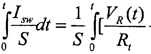 其中, S为所述铁电电容的面积。
4. 如权利要求 1所述的方法, 其特征在于, 在反向偏置所述第一 方形电压脉冲之前, 还包括偏置预极化脉沖, 所述预极化脉冲与所述 第一方形电压脉沖极性相反。
5. 如权利要求 1或 2或 3所述的方法, 其特征在于, 所述第一方 形电压脉沖的上升沿的时间范围为 0.2纳秒至 7.5纳秒。
6. 如权利要求 3所述的方法, 其特征在于, 所述第二方向电压脉 冲使所述铁电薄膜的电畴极化反转, 并且, 所述第二方形电压脉沖与 所述第一脉沖电压脉冲相同。
7. 如权利要求 3所述的方法, 其特征在于, 所述第二方向电压脉 冲的脉冲宽度与所述测试电路的 RC延迟时间基本在同一数量级。
8. 如权利要求 4所述的方法, 其特征在于, 所述预极化脉冲的脉 冲宽度与所述第一脉冲电压脉冲的脉冲宽度相同。
9. 如权利要求 1或 2或 3所述的方法, 其特征在于, 所述电阻包 括测试装置的、 与所述铁电电容串联的等效内阻。
10. 如权利要求】或 2或 3所述的方法, 其特征在于, 基于所述 电滞回线, 进一步测试所述铁电薄膜的疲劳特性、 印刻、 退极化或 / 和保持效应。
1 1. 如权利要求 1或 2或 3所述的方法, 其特征在于, 所述第一 方形电压脉冲的脉冲宽度大于或等于 1纳秒且小于或等于 1微秒。
12. 一种铁电薄膜性能测试装置, 其特征在于, 包括:
测试电路, 其包括所述铁电薄膜等效形成的铁电电容以及与该铁 电电容串联的电阻; 以及
控制模块;
所述控制模块被配置用来:
测量得出所述电阻两端偏置的第一电压] ^(t) ;
根据所迷第一电压 (t)以及偏置于所述测试电路使所述铁电 薄膜的电畴发生极化反转的第一方形电压脉沖的电压 (0 , 计算 得出所述铁电电容的第一偏置电压 (t) ; 得出极化反转电流 / 与所述第一偏置电压 V ή之间的第一关 系式;
基于所述第一关系式、 得出所述铁电薄膜的极化强度 (0与 所述第一偏置电压 ^(0之间的第二关系式; 以及
基于所述第二关系式得出所述铁电薄膜的电滞回线; 其中, 表示时间变量, 所述第一方形电压脉冲的脉沖宽度 长于所述极化反转的时间且与所述极化反转的时间基本在同一 数量级上。
13. 如权利要求 12所述的铁电薄膜性能测试装置, 其特征在于 所述铁电薄膜性能测试装置用于测试绝缘铁电薄膜; 并且,
所述第一关系式为: 
其中, 为所述电阻的阻值;
所述第二关系式为: 
其中, S为所述铁电电容的面积。
14. 如权利要求 12所述的铁电薄膜性能测试装置, 其特征在于, 所述铁电薄膜性能测试装置用于测试漏电铁电薄膜; 所述铁电薄膜性 能测试装置进一步被配置用来:
向所述测试电路依次地偏置 n个第二方形电压脉冲, 在所述 第二方形电压脉冲使所述铁电薄膜的电畴极化反转完毕之后或 者使所述铁电薄膜的铁电电容被充电完毕之后, 测出每个第二方 形电压脉冲偏置下基本稳定的铁电薄膜的漏电流 从而得出 n 个漏电流 ( , 1„ ) ;
依据以下第三关系式: 依次计算得出所述铁电电容的第二偏置电压 ,, ..., ) , 其中, m为大于或等于 1且小于或等于 n的整数; 以及
依据 n个漏电流( IL n ) 以及对应的 n个第二偏置 电压 V ) , 拟合得出所述第二偏置电压 与漏电流 之间函数关系式 = ^)^ ) ;
其中, η个第二方形电压脉冲的脉沖高度分别为( ..., Vn ) , n为大于或等于 1的整数;
并且, 述函数关系式, 述第一关系式被表达为:  其中, 为所述电阻的阻值, /£(0为在第一偏置电压 下所述 铁电电容的漏电流;
所述第二关系式被表达为:
Pf (0 = ]- t = - ^ - - F(Vf (t))]dt,
其中, S为所述铁电电容的面积。
15. 如权利要求 12所述的铁电薄膜性能测试装置, 其特征在于, 还包括:
信号发生电路, 用于向所述测试电路提供偏置的电信号; 采集信号处理电路, 用于将从所述测试电路所采集的数据进行数 据处理;
FPGA控制器;
时钟电路; 以及
计算机装置。
16. 如权利要求 15所述的铁电薄膜性能测试装置, 其特征在于, 所述采集信号处理电路包括:
模拟信号调理电路, 其用于进行信号放大、 衰减以及阻抗匹配; 以及
模数转换器。
17. 如权利要求 16所述的铁电薄膜性能测试装置, 其特征在于, 所述模数转换器的最高釆样率大于或等于 1000 兆 /秒。
18. 如权利要求 15所述的铁电薄膜性能测试装置, 其特征在于, 所述时钟电路孔径时间抖动的最大值小于或等于 1纳秒。
19. 如权利要求 15所述的铁电薄膜性能测试装置, 其特征在于, 所述 FPGA控制的数据接口模块用于对所述采集信号处理电路输出的 数据进行降频、 数据位展宽处理。
20. 一种包括计算机程序代码的计算机程序产品, 用于当所述计 算机程序代码被具有计算机能力的电子设备运行时执行权利要求 1到 1 1中任意一个的方法。
Applications Claiming Priority (2)
| Application Number | Priority Date | Filing Date | Title |
|---|---|---|---|
| CN201110203557.1 | 2011-07-20 | ||
| CN2011102035571A CN102279308A (zh) | 2011-07-20 | 2011-07-20 | 一种绝缘/漏电铁电薄膜电畴反转电流测量与转换为电滞回线的方法 |
Publications (1)
| Publication Number | Publication Date |
|---|---|
| WO2013010298A1 true WO2013010298A1 (zh) | 2013-01-24 |
Family
ID=45104868
Family Applications (1)
| Application Number | Title | Priority Date | Filing Date |
|---|---|---|---|
| PCT/CN2011/001858 Ceased WO2013010298A1 (zh) | 2011-07-20 | 2011-11-04 | 铁电薄膜的性能测试 |
Country Status (2)
| Country | Link |
|---|---|
| CN (1) | CN102279308A (zh) |
| WO (1) | WO2013010298A1 (zh) |
Cited By (1)
| Publication number | Priority date | Publication date | Assignee | Title |
|---|---|---|---|---|
| CN103267883A (zh) * | 2013-05-11 | 2013-08-28 | 桂林理工大学 | 双极性方波脉冲电压绝缘寿命实验的漏电流检测方法 |
Families Citing this family (6)
| Publication number | Priority date | Publication date | Assignee | Title |
|---|---|---|---|---|
| CN102590669B (zh) * | 2012-02-21 | 2014-07-09 | 复旦大学 | 铁电薄膜电畴区域运动速度与矫顽电场关系的测量方法 |
| CN106950444B (zh) * | 2017-03-08 | 2019-07-16 | 天津大学 | 一种铁电材料电滞回线的光学测量方法 |
| CN109709151B (zh) * | 2019-01-30 | 2021-02-09 | 南通大学 | 一种电介质薄膜电学性质测量系统 |
| CN114217156A (zh) * | 2021-12-15 | 2022-03-22 | 中国人民解放军陆军装甲兵学院 | 一种铁电畴运动速度可调的脉冲电压测量法 |
| CN116449137A (zh) * | 2023-05-08 | 2023-07-18 | 四川大学 | 一种储能电介质综合测试系统 |
| CN120314801B (zh) * | 2025-06-18 | 2025-10-21 | 元能科技(厦门)有限公司 | 基于低频eis和恒流脉冲的漏电流测试方法和系统 |
Citations (4)
| Publication number | Priority date | Publication date | Assignee | Title |
|---|---|---|---|---|
| JPH11174098A (ja) * | 1997-12-09 | 1999-07-02 | Fujitsu Ltd | 強誘電体材料の分極特性測定方法 |
| US6466039B1 (en) * | 1999-06-24 | 2002-10-15 | Sony Corporation | Ferroelectric film property measuring device, measuring method therefor and measuring method for semiconductor memory units |
| CN101718810A (zh) * | 2009-11-26 | 2010-06-02 | 复旦大学 | 一种测量漏电铁电薄膜电滞回线的方法 |
| CN102116789A (zh) * | 2011-01-05 | 2011-07-06 | 复旦大学 | 一种铁电畴运动速度可调的脉冲电压测量法 |
Family Cites Families (4)
| Publication number | Priority date | Publication date | Assignee | Title |
|---|---|---|---|---|
| JP2001107238A (ja) * | 1999-07-28 | 2001-04-17 | Sharp Corp | プラチナ電極上の単相ペロブスカイト強誘電体膜およびその形成方法 |
| JP4816200B2 (ja) * | 2006-03-30 | 2011-11-16 | 富士通株式会社 | 強誘電体特性測定装置 |
| CN100582808C (zh) * | 2007-09-17 | 2010-01-20 | 西安交通大学 | 一种铁电材料电滞回线的测量方法 |
| CN101566660A (zh) * | 2009-05-22 | 2009-10-28 | 清华大学 | 一种同时测量铁电材料电滞回线和应变回线的方法及装置 |
-
2011
- 2011-07-20 CN CN2011102035571A patent/CN102279308A/zh active Pending
- 2011-11-04 WO PCT/CN2011/001858 patent/WO2013010298A1/zh not_active Ceased
Patent Citations (4)
| Publication number | Priority date | Publication date | Assignee | Title |
|---|---|---|---|---|
| JPH11174098A (ja) * | 1997-12-09 | 1999-07-02 | Fujitsu Ltd | 強誘電体材料の分極特性測定方法 |
| US6466039B1 (en) * | 1999-06-24 | 2002-10-15 | Sony Corporation | Ferroelectric film property measuring device, measuring method therefor and measuring method for semiconductor memory units |
| CN101718810A (zh) * | 2009-11-26 | 2010-06-02 | 复旦大学 | 一种测量漏电铁电薄膜电滞回线的方法 |
| CN102116789A (zh) * | 2011-01-05 | 2011-07-06 | 复旦大学 | 一种铁电畴运动速度可调的脉冲电压测量法 |
Non-Patent Citations (1)
| Title |
|---|
| LI, YAN ET AL.: "Design of DSP-based Ferroelectric Thin Film Parameters Test System", JOURNAL OF YUNNAN UNIVERSITY (NATURAL SCIENCE VERSION), vol. 27, no. 3A, 2005, pages 396 - 399 * |
Cited By (1)
| Publication number | Priority date | Publication date | Assignee | Title |
|---|---|---|---|---|
| CN103267883A (zh) * | 2013-05-11 | 2013-08-28 | 桂林理工大学 | 双极性方波脉冲电压绝缘寿命实验的漏电流检测方法 |
Also Published As
| Publication number | Publication date |
|---|---|
| CN102279308A (zh) | 2011-12-14 |
Similar Documents
| Publication | Publication Date | Title |
|---|---|---|
| WO2013010298A1 (zh) | 铁电薄膜的性能测试 | |
| Jachalke et al. | How to measure the pyroelectric coefficient? | |
| Hoffmann et al. | Demonstration of high-speed hysteresis-free negative capacitance in ferroelectric Hf 0.5 Zr 0.5 O 2 | |
| Li et al. | Ultrafast polarization switching in thin-film ferroelectrics | |
| Mukherjee et al. | Pulse-based capacitive memory window with high non-destructive read endurance in fully BEOL compatible ferroelectric capacitors | |
| Gao et al. | Frequency dependence on polarization switching measurement in ferroelectric capacitors | |
| Wang et al. | Bit error rate investigation of spin-transfer-switched magnetic tunnel junctions | |
| CN103412210B (zh) | 一种铁电薄膜成核可逆电畴极化强度的测量方法 | |
| TWI280380B (en) | Testing a device | |
| Dehoff et al. | Atomic force microscopy-based experimental setup for studying domain switching dynamics in ferroelectric capacitors | |
| US7965877B2 (en) | Fingerprint sensing device using pulse processing | |
| CN102687029B (zh) | 铁电分析装置及其调节铁电畴极化反转速度的方法 | |
| Grigoriev et al. | Ultrafast electrical measurements of polarization dynamics in ferroelectric thin-film capacitors | |
| Van de Veire et al. | In-plane characterization of PZT thin films for the creation of a general impedance model | |
| JP3944450B2 (ja) | 非破壊的読出しの方法とこの方法を利用する装置 | |
| Massarotto et al. | Versatile experimental setup for FTJ characterization | |
| Gomez et al. | Nano-positive up negative down in binary oxide ferroelectrics | |
| CN102590669B (zh) | 铁电薄膜电畴区域运动速度与矫顽电场关系的测量方法 | |
| Breton et al. | Picosecond time measurement using ultra fast analog memories | |
| CN114217156A (zh) | 一种铁电畴运动速度可调的脉冲电压测量法 | |
| Taylor et al. | Pulse switching characterization of organometallic chemical vapor deposited PbZrxTi1− xO3 thin films for high-density memory applications | |
| Alam et al. | HfZrO ferroelectric characterization and parameterization of response to arbitrary excitation waveform | |
| Mohapatra et al. | Toward accurate ferroelectric polarization estimation in nanoscopic systems | |
| CN116610287A (zh) | 一种基于闪烁噪声的真随机数发生器及实现方法 | |
| Rössle et al. | Time-resolved piezoelectric response in relaxor ferroelectric (Pb0. 88La0. 12)(Zr0. 52Ti0. 48) O3 thin films |
Legal Events
| Date | Code | Title | Description |
|---|---|---|---|
| 121 | Ep: the epo has been informed by wipo that ep was designated in this application |
Ref document number: 11869581 Country of ref document: EP Kind code of ref document: A1 |
|
| NENP | Non-entry into the national phase |
Ref country code: DE |
|
| 122 | Ep: pct application non-entry in european phase |
Ref document number: 11869581 Country of ref document: EP Kind code of ref document: A1 |