WO2012176712A1 - 受動素子の駆動装置及び基板加熱装置 - Google Patents
受動素子の駆動装置及び基板加熱装置 Download PDFInfo
- Publication number
- WO2012176712A1 WO2012176712A1 PCT/JP2012/065388 JP2012065388W WO2012176712A1 WO 2012176712 A1 WO2012176712 A1 WO 2012176712A1 JP 2012065388 W JP2012065388 W JP 2012065388W WO 2012176712 A1 WO2012176712 A1 WO 2012176712A1
- Authority
- WO
- WIPO (PCT)
- Prior art keywords
- voltage
- switching
- terminal
- passive element
- unit
- Prior art date
- Legal status (The legal status is an assumption and is not a legal conclusion. Google has not performed a legal analysis and makes no representation as to the accuracy of the status listed.)
- Ceased
Links
Images





Classifications
-
- H—ELECTRICITY
- H05—ELECTRIC TECHNIQUES NOT OTHERWISE PROVIDED FOR
- H05B—ELECTRIC HEATING; ELECTRIC LIGHT SOURCES NOT OTHERWISE PROVIDED FOR; CIRCUIT ARRANGEMENTS FOR ELECTRIC LIGHT SOURCES, IN GENERAL
- H05B45/00—Circuit arrangements for operating light-emitting diodes [LED]
- H05B45/30—Driver circuits
- H05B45/37—Converter circuits
- H05B45/3725—Switched mode power supply [SMPS]
- H05B45/375—Switched mode power supply [SMPS] using buck topology
-
- Y—GENERAL TAGGING OF NEW TECHNOLOGICAL DEVELOPMENTS; GENERAL TAGGING OF CROSS-SECTIONAL TECHNOLOGIES SPANNING OVER SEVERAL SECTIONS OF THE IPC; TECHNICAL SUBJECTS COVERED BY FORMER USPC CROSS-REFERENCE ART COLLECTIONS [XRACs] AND DIGESTS
- Y02—TECHNOLOGIES OR APPLICATIONS FOR MITIGATION OR ADAPTATION AGAINST CLIMATE CHANGE
- Y02B—CLIMATE CHANGE MITIGATION TECHNOLOGIES RELATED TO BUILDINGS, e.g. HOUSING, HOUSE APPLIANCES OR RELATED END-USER APPLICATIONS
- Y02B20/00—Energy efficient lighting technologies, e.g. halogen lamps or gas discharge lamps
- Y02B20/30—Semiconductor lamps, e.g. solid state lamps [SSL] light emitting diodes [LED] or organic LED [OLED]
Definitions
- the present invention relates to a passive element driving apparatus and a substrate heating apparatus.
- a heat source using an LED array configured by connecting 100 to 200 LEDs in series has been developed.
- a plurality of LED arrays are provided in the heating section, which is a heat source, and by adjusting the amount of power supplied to each LED array, the amount of LED light is adjusted to achieve temperature rise and fall at a desired timing. Techniques to do this are disclosed.
- Pulse width modulation is one of the methods for adjusting LED output.
- PWM Pulse width modulation
- the LED has a voltage-current characteristic that when a voltage equal to or higher than a threshold voltage (Vf) is applied, a current corresponding to the voltage starts to flow. Therefore, in an LED array or the like in which 100 or more LEDs are connected in series, the threshold voltage value at which current starts to flow may increase to several hundred volts.
- Patent Document 2 in an LED lighting device including a transistor (semiconductor switch element) that switches an LED for illumination, it is detected whether the LED is in a non-energized state, and the LED is turned on according to the state.
- a technique for adjusting input power is disclosed. Thereby, the controllability at the time of dimming to low illuminance is improved, and the power loss is reduced.
- JP 2009-253242 A Paragraphs 0032 to 0034, 0044, FIGS. JP 2009-266855 A: Claim 1, paragraphs 0021-0024, FIGS. 1-3
- Patent Documents 1 and 2 describe techniques for reducing the responsiveness and power loss caused by transistor switching control, and solve the problems caused by the voltage-current characteristics of the LED array described above. The method is not described.
- an object of the present invention is to provide a driving device for a passive element with good response and low power loss, and a substrate heating device using the driving device.
- a direct current power supply unit having an intermediate terminal which is an intermediate potential between the high voltage terminal and the low voltage terminal;
- a parallel circuit comprising a passive element and a voltage smoothing capacitor, one end of which is connected to the high voltage terminal;
- a flywheel element connected to the other end of the parallel circuit;
- a snubber circuit connected between the flywheel element and the intermediate terminal;
- a series circuit composed of a current detection unit and a switching unit, connected between the connection point of the flywheel element and the snubber circuit and the low voltage terminal;
- a current control unit that controls switching of the switching unit based on a deviation between a current command value and a current detection value detected by the current detection unit;
- a passive element driving device that controls driving of the passive element by applying a DC voltage by the switching unit in a state where an intermediate voltage is applied between the high voltage terminal and the intermediate terminal.
- a processing container for containing a substrate A heating unit provided with a passive element for heating the substrate in the processing container according to the supplied power;
- a drive device for the passive element comprises: A direct current power supply unit having an intermediate terminal which is an intermediate potential between the high voltage terminal and the low voltage terminal; A parallel circuit comprising the passive element and a voltage smoothing capacitor, one end of which is connected to the high voltage terminal; A flywheel element connected to the other end of the parallel circuit; A snubber circuit connected between the flywheel element and the intermediate terminal; A series circuit composed of a current detection unit and a switching unit, connected between the connection point of the flywheel element and the snubber circuit and the low voltage terminal; A current control unit that controls switching of the switching unit based on a deviation between a current command value and a current detection value detected by the current detection unit;
- a substrate heating apparatus is provided, wherein a DC voltage is applied by the switching unit in a state where an intermediate voltage is applied between the high voltage terminal and the intermediate
- An annealing apparatus 1 is an apparatus that anneals a wafer W having impurities implanted on the surface, and is applied to, for example, a substrate heating apparatus.
- the annealing apparatus 1 includes a processing container 11 and cooling members 12a and 12b.
- the processing container 11 is formed in a flat cylindrical shape, and circular openings are formed on the upper surface side and the lower surface side of the processing container 11.
- the cooling members 12a and 12b are fitted into the openings so as to close the openings. Thereby, the processing space 10 in which an annealing process is performed is formed by the processing container 11 and the cooling members 12a and 12b.
- a loading / unloading port 111 for loading / unloading the wafer W and a gate valve 112 for opening / closing the loading / unloading port 111 are provided on the side wall surface of the processing vessel 11. Further, a gas supply line 113 for supplying an inert gas such as nitrogen gas or argon gas into the processing space 10 is connected to the ceiling surface of the processing container 11. An exhaust line 114 for exhausting the inside of the processing space 10 is connected to the bottom surface side of the processing container 11. The exhaust line 114 is connected to an exhaust means (not shown), and the pressure of the processing space 10 during the annealing process is maintained at a predetermined pressure within a range of 100 to 10,000 Pa, for example.
- an exhaust means not shown
- each support arm 13 (only two are shown in FIG. 1) provided with support pins 131 that support the wafer W from the lower surface side are provided.
- the wafer W can be held via these support pins 131.
- Each support arm 13 can be moved up and down by a lift mechanism (not shown), and the wafer W is transferred by crossing the support pins 131 in the vertical direction with an external wafer transfer mechanism, or a height position for holding the wafer W. Can be adjusted.
- the cooling member 12a faces the upper surface of the wafer W, and a recess 121a is formed on the facing surface.
- the cooling member 12b faces the lower surface of the wafer W, and a recess 121b is formed on the facing surface.
- a heating unit 2 serving as a heat source for the annealing process is formed in the recesses 121a and 121b.
- the heating unit 2 includes a plurality of LEDs 21 (see FIG. 3) that are passive elements of the present embodiment.
- a module 22 is arranged.
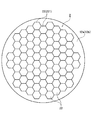
- the LED module 22 of this example has a configuration in which a large number of LEDs 21 are arranged on the plate surface of a hexagonal support substrate 221 (the description of the LEDs 21 is omitted in FIG. 2).
- the plurality of LED modules 22 are arranged in the recesses 121a and 121b of the respective cooling members 12a and 12b so that the upper and lower surfaces of the wafer W are uniformly heated.
- Each LED module 22 has several serial lines of about 100 to 200 LEDs 21.
- the wavelength of light emitted from these LEDs 21 is, for example, in the range of ultraviolet light to near infrared light, and preferably in the range of 0.36 to 1.0 ⁇ m.
- Examples of such a material that emits light in the range of 0.36 to 1.0 ⁇ m include compound semiconductors based on GaN, GaAs, GaP, and the like.
- the LED module 22 is attached to the cooling members 12a and 12b so that the back side of the support substrate 221 is in contact with the cooling surfaces of the cooling members 12a and 12b. Further, light transmitting plates 122a and 122b made of, for example, quartz are attached to the recesses 121a and 121b of the cooling members 12a and 12b so as to cover the LED module 22 from the surface side facing the wafer W. Therefore, the light emitted from the LED array 23 (see FIG. 3) of the LED module 22 passes through the light transmission plates 122a and 122b and reaches the wafer W.
- the space surrounded by the recesses 121a and 121b of the cooling members 12a and 12b and the light transmission plates 122a and 122b is a reduced-pressure atmosphere like the processing space 10, and the upper surfaces of the light transmission plates 122a and 122b and The pressure difference between the lower surfaces is reduced.
- the light transmission plates 122a and 122b can be made thinner than when the recesses 121a and 121b are at atmospheric pressure, and light absorption in the light transmission plates 122a and 122b is suppressed.
- Refrigerant flow paths 123 are formed in the cooling members 12a and 12b with which the support substrate 221 of the LED module 22 comes into contact.
- a refrigerant such as a fluorine-based inert liquid (trade name Fluorinert, Galden (registered trademark)) is supplied as a refrigerant.
- the refrigerant is allowed to flow from the line 124 into the refrigerant flow path 123 and flows from the refrigerant discharge line 125 to the outside.
- the cooling members 12a and 12b can be cooled to 0 ° C. or lower, for example, about ⁇ 50 ° C.
- the schematic configuration of the annealing apparatus 1 has been described above. Next, the electrical configuration of the LED module 22 provided in the annealing apparatus 1, the DC power supply 41 that supplies power to the LED module 22, and the LED driver 31 will be described with reference to FIGS. 3 and 6.
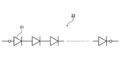
- Each LED module 22 shown in FIGS. 1 and 2 is provided with an LED array 23 composed of a series circuit in which 100 to 200 LEDs 21 are connected in series as shown in FIG. 3, for example.
- Each LED module 22 may be provided with a plurality of LED arrays 23, and these LED arrays 23 may be connected in parallel to a DC power supply unit 41 and an LED driver 31 described below. Since the operation of the DC power supply unit 41 and the LED driver 31 is not changed except that the slope of the voltage-current characteristic is changed, a case where one LED array 23 is driven will be described below.
- the threshold voltage Vf of the entire LED array 23 until the current starts to flow is several hundred volts (example in FIG. 4). Then 270V). For this reason, in the output control using PWM before applying the present invention, a voltage including this threshold voltage (that is, a voltage equal to or higher than the threshold) is turned on / off to the LED array 23.
- an LED driver using PWM control is provided with a current smoothing coil, and the current is turned on / off behind the voltage on / off operation as shown in FIG.
- the switching loss in the LED array 23 is the product of the current value and the voltage value during the period when the current rises and the voltage drops, and the current value and the voltage value during the period when the current falls and the voltage rises. It is represented by the product of
- the DC power supply unit 41 and the LED driver 31 of the present embodiment always apply an intermediate voltage smaller than the threshold voltage shown in FIG. 4 to the LED 21, and add a voltage for PWM control to the intermediate voltage.
- the LED 21 is turned on.
- the DC power supply unit 41, the LED driver 31, and the current control unit 32 constitute a drive device for the LED array 23 (LED 21) according to the present embodiment.
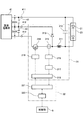
- the DC power supply unit 41 of this example includes a high voltage terminal 411, a low voltage terminal 413, and an intermediate terminal 412 having an intermediate potential between these terminals.
- the DC power supply unit 41 includes, for example, a known rectifier circuit that converts an alternating current supplied from a three-phase power supply into a direct current by PWM rectification.
- the LED array 23 forms a parallel circuit with a current smoothing capacitor 312, and the parallel circuit is connected to the high voltage terminal 411 of the DC power supply unit 41 at one end side in the forward direction and the upstream side of the LED 21. .
- the other end side of the parallel circuit (forward direction, downstream side of the LED 21) is connected to the intermediate terminal 412 of the DC power supply unit 41 via a flywheel coil 311 for current smoothing and a snubber diode 313 forming a snubber circuit.
- the flywheel coil 311 is an example of a flywheel element.
- the potential difference (intermediate voltage) between the high voltage terminal 411 and the intermediate terminal 412 is smaller than the threshold voltage (voltage that turns on when the current starts to flow through the LED array 23) Vf shown in FIG. Is set to This intermediate voltage is constantly applied to the parallel circuit (LED array 23 and capacitor 312).
- a series circuit composed of a Hall IC 315 that forms a current detection unit and a switching FET 314 that is a switching unit. Is provided. For example, a DC voltage of 200 V is applied between the low voltage terminal 413 and the intermediate terminal 412. 6 are provided between the high voltage terminal 411 and the intermediate terminal 412 and between the intermediate terminal 412 and the low voltage terminal 413 shown in FIG. Yes.
- the switching FET 314 When the switching FET 314 is turned off, a circuit of the high voltage terminal 411 ⁇ the LED array 23 ⁇ the flywheel coil 311 ⁇ the snubber diode 313 ⁇ the intermediate terminal 412 is formed, and only the intermediate voltage is applied to the LED array 23.
- the switching FET 314 when the switching FET 314 is turned on, a circuit of the high voltage terminal 411 ⁇ the LED array 23 ⁇ the flywheel coil 311 ⁇ the switching FET 314 ⁇ the low voltage terminal 413 is formed, and the direct current between the intermediate terminal 412 and the low voltage terminal 413 is set to the intermediate voltage. The voltage is added. Then, by changing the on / off interval of the switching FET 314, the voltage applied to the LED 21 can be controlled by changing the average voltage added to the intermediate voltage.
- the current value flowing toward the low voltage terminal 413 is detected by the Hall IC 315 and output as a voltage value corresponding to the current value, and then amplified by the differential amplifier 316 and converted into a balanced signal.
- the V / F converter 317 converts the voltage value into a frequency signal and then differentially outputs it to the current control unit 32 via the line driver 318.
- the frequency signal received by the line driver 321 in the current control unit 32 is counted by the microcomputer 322 and converted into a detected value of the current flowing through the line detected by the Hall IC 315.
- the microcomputer 322 compares a current command value from a device control unit 5 described later with a current detection value. As a result of the comparison, the microcomputer 322 outputs a control signal for increasing / decreasing the pulse width for turning on the switching FET 314 toward the FET driver 319 in a direction to cancel the deviation.
- This control signal transmission / reception is also differentially output via the line drivers 321 and 318.
- the FET driver 319 changes the duty ratio of the time during which the switching FET 314 is turned on based on the control signal from the microcomputer 322, and changes the average DC voltage added to the above-described intermediate power.
- the capacitor 312, flywheel coil 311, snubber diode 313, Hall IC 315, switching FET 314, differential amplifier 316, V / F converter 317, line driver 318, FET driver 319 among the electrical configurations shown in FIG. are provided on a common substrate to constitute the LED driver 31.
- the LED driver 31 is provided between each LED module 22 of the heating unit 2 and a DC power supply unit 41 that supplies power to the LED module 22.
- the current control unit 32 including the line driver 321 that transmits and receives signals to and from the microcomputer 322 and the LED driver 31 illustrated in FIG. 6 is separate from the LED driver 31 and is separated from the LED driver 31.
- the current control unit 32 can acquire a current detection value and output a control signal of the switching FET 314 with a plurality of, for example, four LED drivers 31, and as a result, a plurality of LED modules. 22 output controls can be performed.
- the current control unit 32 constitutes a current control unit of the drive device according to the embodiment. In FIG. 1, a plurality of current control units 32 are shown collectively.
- the current value is converted into a frequency signal and output, and the current signal is calculated after time integration of the frequency signal by the microcomputer 322 on the current control unit 32 side.
- This configuration is resistant to noise generated by the on / off operation of the switching FET 314.
- the DC power supply unit 41 can be disposed in the immediate vicinity of the LED driver 31 to shorten the power transmission distance and supply power with a small number of wires.
- the current control unit 32 since only signal transmission is performed with the current control unit 32, the current control unit 32 may be connected to the LED driver 31 using a thin signal line even from a position away from the LED driver 31. Thereby, the LED driver 31 is miniaturized and the mountability is improved.
- the annealing apparatus 1 having the configuration described above includes an apparatus control unit 5 that performs overall control of the apparatus.
- the apparatus control unit 5 includes a computer having a CPU and a storage unit (not shown), and the storage unit has an operation function of the annealing apparatus 1, that is, loading / unloading of the wafer W, pressure adjustment in the processing space 10, and temperature setting of the annealing process.
- a program in which a group of steps (commands) related to control related to the processing time is recorded.
- This program is stored in a storage medium such as a hard disk, a compact disk, a magnetic optical disk, or a memory card, and installed in the computer therefrom.
- the apparatus control unit 5 detects a temperature detection value from a temperature detection unit (not shown) that detects the temperature of the wafer W arranged in the processing space 10.
- the operation of the annealing apparatus 1 having the above-described configuration will be described.
- the gate valve 112 of the processing container 11 is opened, and an external wafer transfer mechanism is entered from the loading / unloading port 111 to load the wafer W into the processing space 10.
- the wafer transfer mechanism is retracted and the holding height of the wafer W is adjusted.
- the processing chamber 11 is hermetically closed by closing the gate valve 112, and the processing chamber 11 is evacuated from the exhaust line 114, while an inert gas is introduced from the gas supply line 113, and the inside of the processing chamber 11 (processing space)
- the pressure of 10) is adjusted to a predetermined pressure within a range of 100 to 10,000 Pa, for example.
- the refrigerant is passed through the refrigerant flow path 123, and the LED 21 of the LED module 22 is cooled to a temperature of 0 ° C. or lower, preferably ⁇ 50 ° C. or lower.
- an intermediate voltage (for example, 200 V) is constantly applied to the LED array 23 between the high voltage terminal 411 and the intermediate terminal 412.
- the DC voltage between the intermediate terminal 412 and the low voltage terminal 413 is adjusted by PWM and added to the intermediate voltage, so that the LED array 23 is turned on and the output is adjusted. Is done.
- the voltage controlled by the PWM (PWM control voltage shown in FIG. 4) is smaller than the voltage when the intermediate voltage is not applied (the sum of the intermediate voltage and the PWM control voltage shown in FIG. 4).
- Nonlinearity at the time of output adjustment of the LED array 23 is suppressed, and controllability is improved.
- the voltage value turned on / off by the PWM (voltage value VDS shown in FIG. 5) is reduced, and the switching loss can be reduced.
- the switching FET 314 since the voltage value turned on / off by the switching FET 314 becomes small, the level of pressure resistance required for the switching FET 314 can be lowered. As a result, an FET having a low on-resistance and a short switching time can be adopted, and switching loss can be reduced from this viewpoint.
- the output of the LED array 23 is adjusted by such drive control, and the light emitted from the LED modules 22 provided in the upper and lower heating units 2 passes through the light transmission plates 122a and 122b and reaches the wafer W, The temperature is increased by being absorbed by the wafer W. As a result, the wafer W is heated to a target temperature (for example, 1100 ° C.) in a short time such as 1 to 10 seconds, and is implanted in the previous process by maintaining the temperature for a short time of 1 to 10 seconds. A process of combining impurities such as boron and phosphorus with silicon is performed.
- a target temperature for example, 1100 ° C.
- the power supply to the LED array 23 is stopped, and the emission of light from the LEDs 21 is stopped, whereby the heating of the wafer W is stopped.
- the wafer W is rapidly cooled by the inert gas flowing in the processing space 10, and the annealing process is completed.
- the exhaust from the exhaust line 114 is stopped, the inside of the processing space 10 is returned to the atmospheric pressure, the wafer W is unloaded in an operation reverse to that during loading, and a series of operations is completed.
- the LED module 22 that is in contact with the cooling members 12a and 12b is cooled by the refrigerant flowing in the refrigerant flow path 123, and waits until the next wafer W is carried in while suppressing a decrease in the amount of light emission accompanying the temperature rise. .
- the driving device (DC power supply unit 41, LED driver 31, current control unit 32) of the LED array 23 According to the driving device (DC power supply unit 41, LED driver 31, current control unit 32) of the LED array 23 according to the present embodiment, the following effects are obtained.
- An intermediate voltage smaller than a threshold voltage at which the LED 21 of the LED array 23 is turned on is applied to the LED 21, and a DC voltage PWM-controlled by the switching action of the switching FET 314 is added to the intermediate voltage to add current to the LED 21. Flows and the output is adjusted.
- the change width of the voltage added by the PWM control using the switching FET 314 is smaller than that in the case where the intermediate voltage is not applied, so that the switching loss accompanying the on / off operation can be reduced.
- the level of pressure resistance required for the switching FET 314 is lowered, the switching FET 314 can be downsized, and the power loss in the part can be reduced.
- the configuration of the driving device of the LED array 23 is not limited to the example shown in FIG. If an operation of constantly applying an intermediate voltage smaller than the threshold voltage of the LED array 23 and adding a DC voltage controlled by PWM to the intermediate voltage to turn on the LED array 23 is obtained, the configuration Can be changed as appropriate.
- FIG. 7 shows an example in which a snubber FET 313 a is provided as a switching element in a snubber circuit provided between the high voltage terminal 411 and the intermediate terminal 412. 7, the same components as those shown in FIG. 6 are denoted by the same reference numerals as those in FIG.
- the FET driver 319 has a synchronous rectification function.
- the switching FET 314 as a switching element is in an on state
- the snubber FET 313a is in an off state
- the switching FET 314 is in an off state.
- Switching control is performed to turn on the snubber FET 313a.
- the switching elements constituting the switching unit and the snubber circuit are not limited to the case of being constituted by FETs (switching FETs 314 and snubber FETs 313a), and for example, bipolar transistors may be used.
- the passive element drive device (the DC power supply unit 41, the LED driver 31, and the current control unit 32) shown in FIG. 6 and FIG. 7 is not limited to the application to drive control of the LED array 23 (LED 21). Absent.
- the magnetron is known to exhibit the same voltage-current characteristics as the example shown in FIG. 4, and in this drive control as well, this embodiment improves the controllability and obtains the effect of reducing the switching loss. Can do.
- the present embodiment can also be applied to a substrate heating apparatus that includes the magnetron in a heating unit for irradiating a coating liquid containing moisture applied to the wafer W with microwaves and heating the coating liquid.
- the “passive element” described in the claims includes a passive device that is driven by being supplied with electric power.
- Example 1-1 The driving device (DC power supply unit 41, LED driver 31, current control unit 32) using a snubber diode 313 as the snubber circuit shown in FIG. The temperature change of was measured.
- the intermediate voltage was 200 V
- the PWM control voltage was 200 V
- the pulse period of PWM control was 10 ⁇ m seconds
- the duty ratio (PWM%) was 80%.
- the withstand voltage capability of the switching FET 314 is 300V.
- Example 1-2 Using the driving device using the snubber FET 313a as the snubber circuit shown in FIG. 7, power was supplied to the LED array 23 under the same conditions as in Example 1-1, and the temperature change of the switching FET 314 was measured.
- the withstand voltage capability of the switching FET 314 is 300V.
- Example 1-1 Using a drive device that does not apply an intermediate voltage shown in FIG. 8, power was supplied to the LED array 23 under the same conditions as in Example 1-1, and the temperature change of the switching FET 314 was measured.
- the snubber circuit is a capacitor 312 and a shunt resistor 315a is used for current detection.
- the withstand voltage capability of the switching FET 314 is 600V.
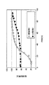
- FIG. 9 shows changes with time in the temperature of the switching FET 314 in each example and comparative example.
- Example 1-1 is indicated by a broken line
- Example 1-2 is indicated by a solid line
- Comparative Example 1-1 is indicated by a two-dot chain line
- Comparative Example 1-2 is indicated by a one-dot chain line.
- the temperature rise width of the switching FET 314 in Examples 1-1 and 1-2 is smaller than the temperature rise width of the switching FET 314 in Comparative Examples 1-1 and 1-2. . It can be evaluated that this is because the voltage applied to the switching FET 314 is reduced and the switching loss is reduced due to the use of the switching FET 314 having a low withstand voltage. Further, comparing the case where the snubber diode 313 is used as the snubber circuit with the case where the snubber FET 313a is used, the temperature increase width of the switching FET 314 is smaller in the case where the snubber FET 313a is used in both the example and the comparative example.
- Example 2 Experimental conditions (Example 2) Using the drive unit shown in FIG. 6, the PWM duty ratio was changed within the range of 0 to 100% under the same conditions as in Example 1-1.
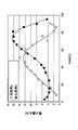
- FIG. 10 shows the change in power usage efficiency with respect to the duty ratio
- FIG. 11 shows the change in power loss. 10 and 11, the results of Example 2 are plotted with white circles, and the results of Comparative Example 2 are plotted with black circles.
- Example 2 In the range where the duty ratio shown in FIG. 10 is about 0 to 30%, the power usage efficiency of Example 2 is smaller than that of Time Comparison Example 2, but in the range beyond this, Example 2 is more power efficient. The use efficiency is higher than that of Comparative Example 2.
- FIG. 11 there is no significant difference in power loss between Example 2 and Comparative Example 2 in the range where the duty ratio is low, but in the range where the duty ratio exceeds 60%, the driving shown in FIG.
- the PWM duty ratio tends to increase. Therefore, it can be said that the driving apparatus of the present embodiment is suitable for such processing.
- an intermediate voltage smaller than the threshold voltage at which the passive element is turned on is applied to the passive element, and the DC voltage controlled by the switching action of the switching unit is further increased.
- a current flows through the passive element to be turned on.
- the level of pressure resistance required for the switching unit is reduced, it is possible to reduce the size of the equipment that constitutes the switching unit, and to reduce power loss in the unit.
- the passive element driving device may have the following characteristics.
- the passive element is a series circuit of a plurality of LEDs.
- the switching unit and the snubber circuit are switching elements, and synchronous rectification is performed to reverse the on / off state between the switching element of the switching unit and the switching element of the snubber circuit.
Landscapes
- Led Devices (AREA)
Abstract
高電圧端子411と低電圧端子413との間に中間電位となる中間端子412を有する直流電源部41と、高電圧端子にその一端側が接続された、受動素子21及び電圧平滑コンデンサ312からなる並列回路と、並列回路の他端側に接続されたフライホイール素子311と、フライホイール素子と中間端子との間に接続されたスナバ回路313と、フライホイール素子及びスナバ回路の接続点と低電圧端子との間に接続された、電流検出部315及びスイッチング部319からなる直列回路と、電流指令値と電流検出部にて検出された電流検出値との偏差分に基づいてスイッチング部のスイッチングを制御する電流制御部32と、を備え、高電圧端子と中間端子との間に中間電圧を印加した状態で、スイッチング部により直流電圧を制御することによって受動素子の駆動を制御することを特徴とする受動素子の駆動装置を提供する。
Description
本発明は、受動素子の駆動装置及び基板加熱装置に関する。
半導体デバイスの製造においては、基板である半導体ウエハ(以下ウエハと記す)を加熱する各種の加熱処理が存在する。なかでも高速の昇温降温が可能であり、ウエハの材料であるシリコンの吸収波長に対応する波長を放出することができるLED(発光ダイオード)を熱源として用いるものが提案されている。
イオンインプランテーション後のアニール処理を行うアニール装置(基板加熱装置)において、例えば100~200個のLEDを直列に接続して構成されるLEDアレイを用いた熱源の開発も行われている。特許文献1には、熱源である加熱部に複数のLEDアレイを設け、各LEDアレイへの給電量を調節することにより、LEDの光量を調節して所望のタイミングでの昇温、降温を実現する技術が開示されている。
LEDの出力を調整する手法の一つとしてパルス幅変調(PWM:Pulse
Width Modulation;以下、PWMという)方式により、受動素子であるLEDへの給電量を制御して発光量を調節する手法がある。LEDはしきい値電圧(Vf)以上の電圧を印加するとその電圧に応じた電流が流れ始めるという電圧-電流特性を有する。よって、100個以上ものLEDが直列に接続されたLEDアレイなどでは、電流が流れ始めるしきい値電圧の値も数百V程度まで大きくなってしまう場合がある。
Width Modulation;以下、PWMという)方式により、受動素子であるLEDへの給電量を制御して発光量を調節する手法がある。LEDはしきい値電圧(Vf)以上の電圧を印加するとその電圧に応じた電流が流れ始めるという電圧-電流特性を有する。よって、100個以上ものLEDが直列に接続されたLEDアレイなどでは、電流が流れ始めるしきい値電圧の値も数百V程度まで大きくなってしまう場合がある。
特許文献2には、照明用のLEDのスイッチングを行うトランジスタ(半導体スイッチ素子)を備えたLED照明装置において、LEDが非通電状態となっているか否かを検出し、その状態に応じてLEDへ入力される電力を調整する技術が開示されている。これにより、低照度に調光した際の制御性を向上させ、電力損失を低減する。
しかし、しきい値電圧の大きなLEDアレイは、単純なオームの法則が適用できない非線形な制御系となる。このため、短時間に電力の供給、停止を繰り返して平均の出力を調節するPWM制御をこのLEDアレイに適用すると、昇温降温動作における制御性が低下してしまう。また、しきい値電圧を含む高圧の電力をオン/オフする動作に耐えうる耐圧性の高いスイッチング素子(FET:Field Effect Transistor)が必要となり、スイッチングロスが増大するといった課題が生じる。
また、特許文献1,2には、トランジスタのスイッチング制御に起因する応答性の低下や電力損失を改善する技術が記載され、先に説明したLEDアレイの電圧-電流特性に起因する課題を解決する手法は記載されていない。
上記課題に対して、本発明は、応答性が良好で電力損失の小さな受動素子の駆動装置、及びこの駆動装置を用いた基板加熱装置を提供することを目的とする。
上記課題を解決するために、本発明のある態様によれば、
高電圧端子と低電圧端子との間に中間電位となる中間端子を有する直流電源部と、
前記高電圧端子にその一端側が接続された、受動素子及び電圧平滑コンデンサからなる並列回路と、
前記並列回路の他端側に接続されたフライホイール素子と、
前記フライホイール素子と前記中間端子との間に接続されたスナバ回路と、
前記フライホイール素子及びスナバ回路の接続点と前記低電圧端子との間に接続された、電流検出部及びスイッチング部からなる直列回路と、
電流指令値と前記電流検出部にて検出された電流検出値との偏差分に基づいて前記スイッチング部のスイッチングを制御する電流制御部と、を備え、
前記高電圧端子と中間端子との間に中間電圧を印加した状態で前記スイッチング部により直流電圧を印加し、前記受動素子の駆動を制御することを特徴とする受動素子の駆動装置が提供される。
高電圧端子と低電圧端子との間に中間電位となる中間端子を有する直流電源部と、
前記高電圧端子にその一端側が接続された、受動素子及び電圧平滑コンデンサからなる並列回路と、
前記並列回路の他端側に接続されたフライホイール素子と、
前記フライホイール素子と前記中間端子との間に接続されたスナバ回路と、
前記フライホイール素子及びスナバ回路の接続点と前記低電圧端子との間に接続された、電流検出部及びスイッチング部からなる直列回路と、
電流指令値と前記電流検出部にて検出された電流検出値との偏差分に基づいて前記スイッチング部のスイッチングを制御する電流制御部と、を備え、
前記高電圧端子と中間端子との間に中間電圧を印加した状態で前記スイッチング部により直流電圧を印加し、前記受動素子の駆動を制御することを特徴とする受動素子の駆動装置が提供される。
また、本発明の他の態様によれば、
基板を収容する処理容器と、
供給される電力に応じて処理容器内の基板を加熱するための受動素子が設けられた加熱部と、
前記受動素子の駆動装置と、を備え、
前記受動素子の駆動装置は、
高電圧端子と低電圧端子との間に中間電位となる中間端子を有する直流電源部と、
前記高電圧端子にその一端側が接続された、前記受動素子及び電圧平滑コンデンサからなる並列回路と、
前記並列回路の他端側に接続されたフライホイール素子と、
前記フライホイール素子と前記中間端子との間に接続されたスナバ回路と、
前記フライホイール素子及びスナバ回路の接続点と前記低電圧端子との間に接続された、電流検出部及びスイッチング部からなる直列回路と、
電流指令値と前記電流検出部にて検出された電流検出値との偏差分に基づいて前記スイッチング部のスイッチングを制御する電流制御部と、を備え、
前記高電圧端子と中間端子との間に中間電圧を印加した状態で前記スイッチング部により直流電圧を印加し、前記受動素子の駆動を制御することを特徴とする基板加熱装置が提供される。
基板を収容する処理容器と、
供給される電力に応じて処理容器内の基板を加熱するための受動素子が設けられた加熱部と、
前記受動素子の駆動装置と、を備え、
前記受動素子の駆動装置は、
高電圧端子と低電圧端子との間に中間電位となる中間端子を有する直流電源部と、
前記高電圧端子にその一端側が接続された、前記受動素子及び電圧平滑コンデンサからなる並列回路と、
前記並列回路の他端側に接続されたフライホイール素子と、
前記フライホイール素子と前記中間端子との間に接続されたスナバ回路と、
前記フライホイール素子及びスナバ回路の接続点と前記低電圧端子との間に接続された、電流検出部及びスイッチング部からなる直列回路と、
電流指令値と前記電流検出部にて検出された電流検出値との偏差分に基づいて前記スイッチング部のスイッチングを制御する電流制御部と、を備え、
前記高電圧端子と中間端子との間に中間電圧を印加した状態で前記スイッチング部により直流電圧を印加し、前記受動素子の駆動を制御することを特徴とする基板加熱装置が提供される。
本発明によれば、応答性が良好で電力損失の小さな受動素子の駆動装置、及びこの駆動装置を用いた基板加熱装置を提供することができる。
以下に添付図面を参照しながら、本発明の実施形態に係るLEDアレイの駆動装置の構成例について説明する。本発明の実施形態に係るアニール装置1は、表面に不純物が注入されたウエハWをアニールする装置であり、例えば基板加熱装置に適用される。
アニール装置1は、処理容器11と冷却部材12a、12bとを有している。処理容器11は、扁平な円筒状に形成され、この処理容器11の上面側及び下面側には円形の開口部が形成されている。冷却部材12a、12bは、その開口部を塞ぐように当該開口部に嵌め込まれている。これにより、処理容器11と冷却部材12a、12bとによって、アニール処理が行われる処理空間10が形成される。
処理容器11の側壁面には、ウエハWの搬入出が行われる搬入出口111及びその開閉を行うゲートバルブ112が設けられている。また、処理容器11の天井面には処理空間10内に窒素ガスやアルゴンガスなどの不活性ガスを供給するためのガス供給ライン113が接続されている。処理容器11の底面側には処理空間10内を排気するための排気ライン114が接続されている。排気ライン114は不図示の排気手段に接続されており、アニール処理を行っている期間中の処理空間10の圧力は例えば100~10000Paの範囲内の所定圧力に維持される。
処理空間10内には、ウエハWを下面側から支持する支持ピン131を先端部に備えた、例えば3本の支持アーム13(図1には2本のみ示してある)が設けられており、これら支持ピン131を介してウエハWを保持することができる。各支持アーム13は不図示の昇降機構により昇降自在となっており、外部のウエハ搬送機構と上下方向に支持ピン131を交差させてウエハWの受け渡しを行ったり、ウエハWを保持する高さ位置を調整したりすることができる。
冷却部材12aは、ウエハWの上面と対向し、その対向面には凹部121aが形成されている。同様に、冷却部材12bは、ウエハWの下面と対向し、その対向面には凹部121bが形成されている。この凹部121a、121b内にはアニール処理の熱源となる加熱部2が形成されており、加熱部2には本実施の形態の受動素子である多数個のLED21(図3参照)を備えたLEDモジュール22が配置されている。
図2に示すように本例のLEDモジュール22は六角形の支持基板221の板面に多数のLED21を配置した構成となっている(図2ではLED21の記載を省略してある)。そして各冷却部材12a、12bの凹部121a、121b内に、複数のLEDモジュール22を配置することによりウエハWの上面及び下面を満遍なく加熱する構成となっている。
各LEDモジュール22には、100~200個程度のLED21の直列ラインが数ラインある。これらのLED21から射出される光の波長は、例えば紫外光~近赤外光の範囲、好ましくは0.36~1.0μmの範囲が好ましい。このような0.36~1.0μmの範囲の光を射出する材料としてはGaN、GaAs、GaP等をベースとした化合物半導体が例示される。この中では、特に加熱対象として用いられるシリコン製のウエハWにおける吸収率が高い850~970nm付近の放射波長を有するGaAs系の材料からなるLED21がさらに好適である。
LEDモジュール22は支持基板221の裏面側が冷却部材12a、12bの冷却面と接触するように冷却部材12a、12bに取り付けられている。また、冷却部材12a、12bの凹部121a、121bには、ウエハWと対向する表面側からLEDモジュール22を覆うように、例えば石英などからなる光透過板122a,122bが取り付けられている。従って、LEDモジュール22のLEDアレイ23(図3参照)から射出された光は光透過板122a,122bを透過してウエハWに到達することになる。
また、冷却部材12a、12bの凹部121a、121bと光透過板122a、122bとで囲まれた空間は、処理空間10と同様に減圧雰囲気となっており、各光透過板122a,122bの上面及び下面間の圧力差を小さくしている。これにより、凹部121a、121b内が大気圧である場合に比べて光透過板122a、122bを薄くすることが可能となり、光透過板122a、122bにおける光の吸収が抑えられる。
LEDモジュール22の支持基板221が接触する冷却部材12a、12bには冷媒流路123が形成されており、例えばフッ素系不活性液体(商品名フロリナート、ガルデン(登録商標))などの冷媒を冷媒供給ライン124から当該冷媒流路123内に通流させて冷媒排出ライン125から外部に流す。これにより、冷却部材12a、12bを0℃以下の例えば-50℃程度に冷却することができる。
以上、アニール装置1の概略構成を説明した。次に、アニール装置1に設けられているLEDモジュール22、及びこのLEDモジュール22に電力を供給する直流電源41並びにLEDドライバ31の電気的構成について図3、図6を参照しながら説明する。
図1、図2に示した各LEDモジュール22には、例えば図3に示すように、100~200個のLED21を直列に接続した直列回路からなるLEDアレイ23が設けられている。各LEDモジュール22には、LEDアレイ23を複数個設け、以下に説明する直流電源部41及びLEDドライバ31に、これらのLEDアレイ23を並列に接続してもよい。電圧-電流特性の傾きが変化する他は直流電源部41やLEDドライバ31の作用は変わらないので、以下、1個のLEDアレイ23を駆動する場合について説明する。
図4に示すように、多数のLED21を直列に接続したLEDアレイ23は、電流が流れ始めるまでのLEDアレイ23全体のしきい値電圧Vfの値が数百Vにもなる(図4の例では270V)。このため、本発明を適用する前のPWMを利用した出力制御ではこのしきい値電圧を含む電圧(すなわち、しきい値以上の電圧)がLEDアレイ23にオン/オフされる。
一般に、PWM制御を用いたLEDドライバには、電流平滑用のコイルが設けられており、図5に示すように電圧のオン/オフ動作に遅れて電流がオン/オフされる。このときLEDアレイ23におけるスイッチングロスは、電流が上昇し、電圧が降下する期間中の電流値と電圧値との積、及び電流が降下し、電圧が上昇する期間中の電流値と電圧値との積で表される。
このため、スイッチングにより印加される電圧値が高くなると、前記スイッチングロスも大きくなる。また高電圧が印加される場合、スイッチング素子としては耐圧性の高いFET等が必要となるが、このようなFETはオン抵抗が大きいため、消費電力のロスも大きくなる。これに加えて耐圧性の高いFETは、オン/オフの切り替え時間も長く、図5に示したスイッチングロスが引き起こされる期間も長くなるため、この点でもスイッチングロスが大きくなる。
そこで本実施の形態の直流電源部41及びLEDドライバ31は、図4に示したしきい値電圧よりも小さな中間電圧をLED21に常時印加しておき、この中間電圧にPWM制御用の電圧を加算してLED21をオンの状態にする点に特徴を有している。以下、図6を参照しながら直流電源部41、LEDドライバ31及び電流制御部32の構成について説明する。これら直流電源部41、LEDドライバ31及び電流制御部32は、本実施の形態に係わるLEDアレイ23(LED21)の駆動装置を構成している。
図6に示すように、本例の直流電源部41は高電圧端子411と、低電圧端子413と、これらの端子の中間の電位となる中間端子412とを備えている。直流電源部41は例えば三相電源から供給された交流電流をPWM整流して直流電流に変換する公知の整流回路などから構成されている。一方、LEDアレイ23は電流平滑用のコンデンサ312と並列回路を形成しており、当該並列回路はLED21の順方向、上流側の一端側が前記直流電源部41の高電圧端子411に接続されている。
一方、前記並列回路の他端側(LED21の順方向、下流側)は、電流平滑用のフライホイールコイル311及びスナバ回路をなすスナバダイオード313を介して直流電源部41の中間端子412に接続されている。なお、フライホイールコイル311は、フライホイール素子の一例である。高電圧端子411と中間端子412との間の電位差(中間電圧)は、図4に示すしきい値電圧(LEDアレイ23に電流が流れ始めてオンになる電圧)Vfよりも小さい値である例えば200Vに設定されている。そして、この中間電圧が前記並列回路(LEDアレイ23及びコンデンサ312)に常時印加されている。中間電圧は、しきい値の例えば60~95%、より好ましくは80~95%の値に設定することにより、LEDアレイ23の出力制御の非線形性を緩和し、またスイッチングロスを低減する効果が高くなる。
また、フライホイールコイル311とスナバダイオード313の接続点と、直流電源部41の低電圧端子413との間には、電流検出部をなすホールIC315とスイッチング部であるスイッチングFET314とからなる直列回路が設けられている。低電圧端子413と中間端子412との間には、例えば200Vの直流電圧が印加されている。図6中に示す高電圧端子411と中間端子412との間、及び中間端子412と低電圧端子413との間には、直流電源部41側の電圧平滑用のコンデンサ42、43が設けられている。
そして、スイッチングFET314をオフにすると高電圧端子411→LEDアレイ23→フライホイールコイル311→スナバダイオード313→中間端子412という回路が形成されて中間電圧のみがLEDアレイ23に印加される。一方、スイッチングFET314をオンにすると高電圧端子411→LEDアレイ23→フライホイールコイル311→スイッチングFET314→低電圧端子413という回路が形成され、前記中間電圧に中間端子412-低電圧端子413間の直流電圧が加算される。そして、スイッチングFET314のオン/オフ間隔を変化させることにより、中間電圧に加算される平均の電圧を変化させてLED21に印加される電圧を制御することができる。
低電圧端子413へ向けて流れる電流値は、ホールIC315にて検出され電流値に対応する電圧値として出力された後、差動アンプ316にて増幅されると共に、平衡信号に変換される。V/Fコンバータ317では、前記電圧値を周波数信号に変換してからラインドライバ318を介して電流制御部32へ差動出力する。
電流制御部32内のラインドライバ321で受信された周波数信号はマイコン322でカウントされて、ホールIC315で検出される線路を流れる電流の検出値に変換される。マイコン322では、後述する装置制御部5からの電流指令値と電流検出値とを比較する。マイコン322では、比較の結果、その偏差分を解消する方向にスイッチングFET314をオンにするパルス幅を増減させるための制御信号をFETドライバ319へ向けて出力する。この制御信号の送受信もラインドライバ321、318を介して差動出力される。
FETドライバ319は、マイコン322からの制御信号に基づいてスイッチングFET314のオンを行う時間のデューティー比を変化させ、既述の中間電力に加算される平均の直流電圧を変化させる。
本例では図6に示した電気的構成のうち、コンデンサ312、フライホイールコイル311、スナバダイオード313、ホールIC315、スイッチングFET314、差動アンプ316、V/Fコンバータ317、ラインドライバ318、FETドライバ319は、共通の基板上に設けられてLEDドライバ31を構成している。図1に示すようにLEDドライバ31は、加熱部2の各LEDモジュール22とLEDモジュール22に電力を供給する直流電源部41との間設けられている。
一方、図6に示すマイコン322やLEDドライバ31との間で信号の送受信を行うラインドライバ321を含む電流制御部32は、LEDドライバ31とは別体となっており、LEDドライバ31から離れた位置に配置されている(図1)。そして、電流制御部32は複数個、例えば4個のLEDドライバ31との間で各々電流検出値の取得、スイッチングFET314の制御信号の出力を行うことが可能であり、この結果、複数のLEDモジュール22の出力制御を行うことができる。電流制御部32は、実施の形態に係わる駆動装置の電流制御部を構成している。図1では、複数個の電流制御部32を総括的に示している。
既述のようにLEDドライバ31からは、電流値を周波数信号に変換して出力し、電流制御部32側のマイコン322にて周波数信号を時間積分してから電流検出値を算出することにより、スイッチングFET314のオン/オフ動作で発生するノイズに強い構成となっている。また、LEDドライバ31と電流制御部32との間の信号の送受信を差動で行うことにより、LEDドライバ31から離れた位置に電流制御部32を配置しても信頼性の高い信号の送受信ができる。この結果、直流電源部41はLEDドライバ31の直近に配置して送電距離を短くし、少ない電線で電力を供給できる。一方、電流制御部32との間では信号送信を行うだけなので、電流制御部32は、LEDドライバ31から離れた位置からであっても細い信号線を用いてLEDドライバ31と接続すれば足りる。これにより、LEDドライバ31を小型化して、実装性を向上させている。
以上に説明した構成を備えたアニール装置1は当該装置全体を統括制御する装置制御部5を備えている。装置制御部5は図示しないCPUと記憶部とを備えたコンピュータからなり、記憶部にはアニール装置1の作用機能、即ちウエハWの搬入出や処理空間10内の圧力調整、アニール処理の温度設定や処理時間などに係わる制御についてのステップ(命令)群が組まれたプログラムが記録されている。このプログラムは、例えばハードディスク、コンパクトディスク、マグネットオプティカルディスク、メモリーカード等の記憶媒体に格納され、そこからコンピュータにインストールされる。
特に電流制御部32、LEDドライバ31を利用したLEDアレイ23の出力調整につき装置制御部5は、処理空間10内に配置されたウエハWの温度を検出する不図示の温度検出部から温度検出値を取得し、アニール処理の設定温度と温度検出値とを比較し、その偏差分を解消する方向にLEDアレイ23の出力を調整するよう、各電流制御部32に電力指令値を出力する機能を備えている。
上述の構成を備えたアニール装置1の動作について説明する。処理容器11のゲートバルブ112を開き、搬入出口111から、外部のウエハ搬送機構を進入させて処理空間10にウエハWを搬入する。支持ピン131上にウエハWを載置したら、ウエハ搬送機構を退避させ、ウエハWの保持高さを調節する。次いで、ゲートバルブ112を閉じて処理容器11内を密閉状態とし、排気ライン114から処理容器11内の排気を行う一方、ガス供給ライン113から不活性ガスを導入し、処理容器11内(処理空間10)の圧力を例えば100~10000Paの範囲内の所定の圧力に調節する。
一方、冷却部材12a、12bでは、冷媒流路123に冷媒を通流させ、LEDモジュール22のLED21を0℃以下、好ましくは-50℃以下の温度に冷却しておく。
そして、各直流電源部41から電力の供給を開始すると共に、LEDドライバ31を動作させてLEDアレイ23の出力調整を行う。このとき、図4、図6を用いて説明したように、LEDアレイ23には高電圧端子411-中間端子412間に中間電圧(例えば200V)が常時印加されている。そして、マイコン322からの電力指令値に基づき、中間端子412-低電圧端子413間の直流電圧がPWMによって調整されて前記中間電圧に加算されることによりLEDアレイ23がオンとなり、その出力が調整される。
このとき、PWMにより制御される電圧(図4に示したPWM制御電圧)が、中間電圧を印加しない場合の電圧(同図に示した中間電圧とPWM制御電圧との合計)よりも小さいので、LEDアレイ23の出力調整時の非線形性が抑えられて制御性が向上する。また、スイッチングFET314でスイッチングする電圧が小さくなる結果、PWMによってオン/オフされる電圧値(図5に示した電圧値VDS)が小さくなり、スイッチングロスを低減できる。
また、スイッチングFET314にてオン/オフされる電圧値が小さくなることにより、スイッチングFET314に要求される耐圧性のレベルを低くできる。この結果、オン抵抗が低く、切り替え時間の短いFETを採用することが可能となり、この観点でもスイッチングロスを低減できる。
このような駆動制御によりLEDアレイ23の出力が調整され、上下の加熱部2に設けられたLEDモジュール22から射出された光は、光透過板122a,122bを透過してウエハWに到達し、当該ウエハWに吸収されてその温度を上昇させる。この結果、ウエハWは例えば1~10秒程度の短い時間で目標温度(例えば1100℃)まで昇温され、1~10秒程度の短時間当該温度を保持することにより、前工程で注入されたホウ素やリンなどの不純物をシリコンと結合させる処理が行われる。
そして、予め設定した時間が経過したら、LEDアレイ23への電力供給を停止し、LED21からの光の射出を止めることにより、ウエハWの加熱が停止される。ウエハWは、処理空間10内を流れる不活性ガスにより急速に冷却されて、アニール処理を終了する。ウエハWの冷却後、排気ライン114からの排気を停止して、処理空間10内を大気圧に戻し、搬入時とは逆の動作でウエハWを搬出して一連の動作を終える。
一方、冷却部材12a、12bと接触するLEDモジュール22は、冷媒流路123内を流れる冷媒により冷却され、温度上昇に伴う発光量の低下を抑えつつ、次のウエハWが搬入されるまで待機する。
本実施の形態に係わるLEDアレイ23の駆動装置(直流電源部41、LEDドライバ31、電流制御部32)によれば以下の効果がある。LEDアレイ23のLED21がオンになるしきい値電圧よりも小さい中間電圧を当該LED21に印加し、さらにスイッチングFET314のスイッチング作用によりPWM制御される直流電圧を前記中間電圧に加算することによりLED21に電流が流れてオンの状態となると共にその出力が調整される。この結果、スイッチングFET314を利用してPWM制御により加算される電圧の変化幅が、中間電圧を印加しない場合に比べて小さくなるので、オン/オフ動作に伴うスイッチング損失を小さくすることができる。また、スイッチングFET314に要求される耐圧性のレベルも低くなるので、当該スイッチングFET314を小型化することが可能となり、当該部における電力損失も低減することができる。
ここで、LEDアレイ23の駆動装置の構成は図6に示した例に限定されるものではない。LEDアレイ23のしきい値電圧よりも小さな中間電圧を常時印加し、この中間電圧にPWMにより制御された直流電圧を加算してLEDアレイ23をオンの状態とする作用が得られれば、その構成は適宜変更できる。例えば、図7は高電圧端子411-中間端子412間に設けられるスナバ回路に、スイッチング素子としてスナバFET313aを設けた例を示している。図7において、図6に示したものと同様の構成要素には、図6と同じ符号を付してある。
スナバFET313aによりスナバ回路を構成する場合には、FETドライバ319は同期整流機能を備え、スイッチング素子であるスイッチングFET314がオンの状態のときスナバFET313aをオフの状態とし、スイッチングFET314がオフの状態のときスナバFET313aをオンの状態とするスイッチング制御を行う。ここでスイッチング部やスナバ回路を構成するスイッチング素子はFET(スイッチングFET314、スナバFET313a)によって構成する場合に限られず、例えばバイポーラトランジスタなどを用いてもよい。
また、図6や図7に示した受動素子の駆動装置(直流電源部41、LEDドライバ31、電流制御部32)は、LEDアレイ23(LED21)の駆動制御に適用する場合に限られるものではない。例えばマグネトロンは、図4に示した例と同様の電圧-電流特性を示すことが知られており、その駆動制御においても本実施形態は制御性を向上させ、スイッチングロスを低減する効果を得ることができる。例えばウエハWに塗布された水分を含む塗布液にマイクロ波を照射して、当該塗布液を加熱するための加熱部に前記マグネトロンを備えた基板加熱装置などにも本実施形態は適用できる。この場合、特許請求の範囲に記載の「受動素子」は電力を供給されて駆動する受動装置も含んでいることになる。
(実験1)
中間電圧にPWMで調整された直流電圧を加算する本実施形態の駆動装置、及び中間電圧を印加しない駆動装置を用いてLEDアレイ23に電力を供給し、スイッチングFET314の温度変化を調べた。
中間電圧にPWMで調整された直流電圧を加算する本実施形態の駆動装置、及び中間電圧を印加しない駆動装置を用いてLEDアレイ23に電力を供給し、スイッチングFET314の温度変化を調べた。
A.実験条件
(実施例1-1)
図6に示したスナバ回路としてスナバダイオード313を用いる駆動装置(直流電源部41、LEDドライバ31、電流制御部32)を用い、LEDアレイ23に平均電圧160V、400mAの電力を供給してスイッチングFET314の温度変化を計測した。中間電圧は200V、PWM制御電圧は200Vであり、PWM制御のパルス周期は10μm秒、デューティー比(PWM%)は80%とした。スイッチングFET314の耐圧能力は300Vである。
(実施例1-1)
図6に示したスナバ回路としてスナバダイオード313を用いる駆動装置(直流電源部41、LEDドライバ31、電流制御部32)を用い、LEDアレイ23に平均電圧160V、400mAの電力を供給してスイッチングFET314の温度変化を計測した。中間電圧は200V、PWM制御電圧は200Vであり、PWM制御のパルス周期は10μm秒、デューティー比(PWM%)は80%とした。スイッチングFET314の耐圧能力は300Vである。
(実施例1-2)
図7に示したスナバ回路としてスナバFET313aを用いる駆動装置を用い、(実施例1-1)と同様の条件でLEDアレイ23に電力を供給し、スイッチングFET314の温度変化を計測した。スイッチングFET314の耐圧能力は300Vである。
図7に示したスナバ回路としてスナバFET313aを用いる駆動装置を用い、(実施例1-1)と同様の条件でLEDアレイ23に電力を供給し、スイッチングFET314の温度変化を計測した。スイッチングFET314の耐圧能力は300Vである。
(比較例1-1)
図8に示す、中間電圧の印加を行わない駆動装置を用い、(実施例1-1)と同様の条件でLEDアレイ23に電力を供給し、スイッチングFET314の温度変化を計測した。図8の駆動装置においてスナバ回路はコンデンサ312であり、電流検出にはシャント抵抗器315aを用いた。スイッチングFET314の耐圧能力は600Vである。
図8に示す、中間電圧の印加を行わない駆動装置を用い、(実施例1-1)と同様の条件でLEDアレイ23に電力を供給し、スイッチングFET314の温度変化を計測した。図8の駆動装置においてスナバ回路はコンデンサ312であり、電流検出にはシャント抵抗器315aを用いた。スイッチングFET314の耐圧能力は600Vである。
(比較例1-2)
スナバ回路としてスナバFET313aを用いた点以外は、(比較例1-1)と同様の条件でスイッチングFET314の温度を計測した。スイッチングFET314の耐圧能力は300Vである。
スナバ回路としてスナバFET313aを用いた点以外は、(比較例1-1)と同様の条件でスイッチングFET314の温度を計測した。スイッチングFET314の耐圧能力は300Vである。
B.実験結果
各実施例、比較例におけるスイッチングFET314の温度の経時変化を図9に示す。図9には、実施例1-1を破線、実施例1-2を実線、比較例1-1を二点鎖線、比較例1-2を一点鎖線で示してある。
各実施例、比較例におけるスイッチングFET314の温度の経時変化を図9に示す。図9には、実施例1-1を破線、実施例1-2を実線、比較例1-1を二点鎖線、比較例1-2を一点鎖線で示してある。
図9に示した結果によれば、実施例1-1、1-2におけるスイッチングFET314の温度上昇幅が、比較例1-1、1-2におけるスイッチングFET314の温度上昇幅よりも小さくなっている。これは、スイッチングFET314に加わる電圧が小さくなったこと、耐圧性の低いスイッチングFET314を使用したことに伴うスイッチングロスの減少に起因するものと評価できる。また、スナバ回路としてスナバダイオード313を用いる場合とスナバFET313aを用いる場合とを比べると、実施例、比較例のいずれにおいてもスナバFET313aを用いる場合の方がスイッチングFET314の温度上昇幅が小さい。
(実験2)
実施例1-1、比較例1-1におけるLEDアレイ23の駆動実験においてPWMのデューティー比(PWM%)を変化させ、電力の使用効率及び電力損失を算出した。
実施例1-1、比較例1-1におけるLEDアレイ23の駆動実験においてPWMのデューティー比(PWM%)を変化させ、電力の使用効率及び電力損失を算出した。
A.実験条件
(実施例2)
図6に示す駆動装置を用い、(実施例1-1)と同様の条件の下、PWMのデューティー比を0~100%の範囲内で変化させた。
(実施例2)
図6に示す駆動装置を用い、(実施例1-1)と同様の条件の下、PWMのデューティー比を0~100%の範囲内で変化させた。
(比較例2)
図8に示す駆動装置を用い、(比較例1-1)と同様の条件の下、PWMのデューティー比を0~100%の範囲内で変化させた。
図8に示す駆動装置を用い、(比較例1-1)と同様の条件の下、PWMのデューティー比を0~100%の範囲内で変化させた。
B.実験結果
実施例2、比較例2の実験結果において、デューティー比に対する電力の使用効率の変化を図10に示し、電力損失の変化を図11に示す。図10、図11において、実施例2の結果を白丸でプロットし、比較例2の結果を黒丸でプロットした。
実施例2、比較例2の実験結果において、デューティー比に対する電力の使用効率の変化を図10に示し、電力損失の変化を図11に示す。図10、図11において、実施例2の結果を白丸でプロットし、比較例2の結果を黒丸でプロットした。
図10に示したデューティー比が0~30%程度の範囲では、実施例2の方が時比較例2よりも電力の使用効率は小さいが、これ以上の範囲では実施例2の方が電力の使用効率は比較例2よりも高い。図11に示すように、デューティー比の低い範囲では実施例2と比較例2とで電力の損失量に大きな差は見られないが、デューティー比が60%を超えた範囲では、図6の駆動装置(実施例2)と図8の駆動装置(比較例2)とで電力の損失量の差が急激に大きくなっている。ウエハWを短時間で高温に加熱するアニール装置1などでは、PWMのデューティー比は高くなる傾向となるので、本実施の形態の駆動装置はこのような処理に適しているといえる。
以上に説明したように、本実施形態によれば、受動素子がオンになるしきい値電圧よりも小さい中間電圧を当該受動素子に印加し、さらにスイッチング部のスイッチング作用により制御される直流電圧を前記中間電圧に加算することにより受動素子に電流が流れてオンの状態となる。この結果、スイッチング部を利用して加算される電圧の変化幅が小さくなるので、オン/オフ動作に伴うスイッチング損失を小さくすることができる。また、スイッチング部に要求される耐圧性のレベルも低くなるので、スイッチング部を構成する機器を小型化することが可能となり、当該部における電力損失も低減することができる。
なお、前記受動素子の駆動装置は以下の特徴を備えていてもよい。
(a)前記受動素子は複数のLEDの直列回路であること。
(b)前記スイッチング部及びスナバ回路はスイッチング素子であり、スイッチング部のスイッチング素子とスナバ回路のスイッチング素子とのオン/オフの状態を反転させる同期整流が行われること。
以上、添付図面を参照しながら本発明の好適な実施形態について詳細に説明したが、本発明はかかる例に限定されない。本発明の属する技術の分野における通常の知識を有する者であれば、特許請求の範囲に記載された技術的思想の範疇において、各種の変更例または修正例に想到し得ることは明らかであり、これらについても、当然に本発明の技術的範囲に属するものと了解される。
本国際出願は、2011年6月22日に出願された日本国特許出願2011-138562号に基づく優先権を主張するものであり、その全内容を本国際出願に援用する。
W ウエハ
1 アニール装置
21 LED
22 LEDモジュール
23 LEDアレイ
31 LEDドライバ
311 フライホイールコイル
312 コンデンサ
313 スナバダイオード
313a スナバFET
314 スイッチングFET
315 ホールIC
319 FETドライバ
32 電流制御部
322 マイコン
41 直流電源部
411 高電圧端子
412 中間端子
413 低電圧端子
5 装置制御部
1 アニール装置
21 LED
22 LEDモジュール
23 LEDアレイ
31 LEDドライバ
311 フライホイールコイル
312 コンデンサ
313 スナバダイオード
313a スナバFET
314 スイッチングFET
315 ホールIC
319 FETドライバ
32 電流制御部
322 マイコン
41 直流電源部
411 高電圧端子
412 中間端子
413 低電圧端子
5 装置制御部
Claims (6)
- 高電圧端子と低電圧端子との間に中間電位となる中間端子を有する直流電源部と、
前記高電圧端子にその一端側が接続された、受動素子及び電圧平滑コンデンサからなる並列回路と、
この並列回路の他端側に接続されたフライホイール素子と、
前記フライホイール素子と前記中間端子との間に接続されたスナバ回路と、
前記フライホイール素子及びスナバ回路の接続点と前記低電圧端子との間に接続された、電流検出部及びスイッチング部からなる直列回路と、
電流指令値と前記電流検出部にて検出された電流検出値との偏差分に基づいて前記スイッチング部のスイッチングを制御する電流制御部と、を備え、
前記高電圧端子と前記中間端子との間に中間電圧を印加した状態で前記スイッチング部により直流電圧を印加し、前記受動素子の駆動を制御することを特徴とする受動素子の駆動装置。 - 前記中間電圧は、前記受動素子がオンになるしきい値電圧よりも小さい値に設定されることを特徴とする請求項1に記載の受動素子の駆動装置。
- 前記直流電圧を前記中間電圧に加算した合計電圧によって前記受動素子の駆動を制御することを特徴とする請求項1に記載の受動素子の駆動装置。
- 前記受動素子は複数のLEDの直列回路であることを特徴とする請求項1に記載の受動素子の駆動装置。
- 前記スイッチング部及びスナバ回路はスイッチング素子であり、スイッチング部のスイッチング素子とスナバ回路のスイッチング素子とのオン又はオフの状態を反転させる同期整流が行われることを特徴とする請求項1に記載の受動素子の駆動装置。
- 基板を収容する処理容器と、
供給される電力に応じて処理容器内の基板を加熱するための受動素子が設けられた加熱部と、
前記受動素子の駆動装置と、を備え、
前記受動素子の駆動装置は、
高電圧端子と低電圧端子との間に中間電位となる中間端子を有する直流電源部と、
前記高電圧端子にその一端側が接続された、前記受動素子及び電圧平滑コンデンサからなる並列回路と、
前記並列回路の他端側に接続されたフライホイール素子と、
前記フライホイール素子と前記中間端子との間に接続されたスナバ回路と、
前記フライホイール素子及びスナバ回路の接続点と前記低電圧端子との間に接続された、電流検出部及びスイッチング部からなる直列回路と、
電流指令値と前記電流検出部にて検出された電流検出値との偏差分に基づいて前記スイッチング部のスイッチングを制御する電流制御部と、を備え、
前記高電圧端子と中間端子との間に中間電圧を印加した状態で前記スイッチング部により直流電圧を印加し、前記受動素子の駆動を制御することを特徴とする基板加熱装置。
Applications Claiming Priority (2)
| Application Number | Priority Date | Filing Date | Title |
|---|---|---|---|
| JP2011-138562 | 2011-06-22 | ||
| JP2011138562A JP2013008727A (ja) | 2011-06-22 | 2011-06-22 | 受動素子の駆動装置及び基板加熱装置 |
Publications (1)
| Publication Number | Publication Date |
|---|---|
| WO2012176712A1 true WO2012176712A1 (ja) | 2012-12-27 |
Family
ID=47422550
Family Applications (1)
| Application Number | Title | Priority Date | Filing Date |
|---|---|---|---|
| PCT/JP2012/065388 Ceased WO2012176712A1 (ja) | 2011-06-22 | 2012-06-15 | 受動素子の駆動装置及び基板加熱装置 |
Country Status (3)
| Country | Link |
|---|---|
| JP (1) | JP2013008727A (ja) |
| TW (1) | TW201306646A (ja) |
| WO (1) | WO2012176712A1 (ja) |
Families Citing this family (1)
| Publication number | Priority date | Publication date | Assignee | Title |
|---|---|---|---|---|
| JP7480656B2 (ja) * | 2020-09-23 | 2024-05-10 | ウシオ電機株式会社 | 光源ユニット及び加熱処理装置 |
Citations (4)
| Publication number | Priority date | Publication date | Assignee | Title |
|---|---|---|---|---|
| JPH10190101A (ja) * | 1996-12-26 | 1998-07-21 | Fuji Xerox Co Ltd | 半導体レーザ駆動装置および画像記録装置 |
| JP2008192717A (ja) * | 2007-02-02 | 2008-08-21 | Seiko Epson Corp | レーザ光源装置、プロジェクタおよびモニタ装置、並びに、半導体レーザ駆動方法 |
| JP2009253242A (ja) * | 2008-04-11 | 2009-10-29 | Tokyo Electron Ltd | アニール装置 |
| JP2010205778A (ja) * | 2009-02-27 | 2010-09-16 | Toshiba Lighting & Technology Corp | 電源装置 |
-
2011
- 2011-06-22 JP JP2011138562A patent/JP2013008727A/ja not_active Withdrawn
-
2012
- 2012-06-15 WO PCT/JP2012/065388 patent/WO2012176712A1/ja not_active Ceased
- 2012-06-21 TW TW101122196A patent/TW201306646A/zh unknown
Patent Citations (4)
| Publication number | Priority date | Publication date | Assignee | Title |
|---|---|---|---|---|
| JPH10190101A (ja) * | 1996-12-26 | 1998-07-21 | Fuji Xerox Co Ltd | 半導体レーザ駆動装置および画像記録装置 |
| JP2008192717A (ja) * | 2007-02-02 | 2008-08-21 | Seiko Epson Corp | レーザ光源装置、プロジェクタおよびモニタ装置、並びに、半導体レーザ駆動方法 |
| JP2009253242A (ja) * | 2008-04-11 | 2009-10-29 | Tokyo Electron Ltd | アニール装置 |
| JP2010205778A (ja) * | 2009-02-27 | 2010-09-16 | Toshiba Lighting & Technology Corp | 電源装置 |
Also Published As
| Publication number | Publication date |
|---|---|
| TW201306646A (zh) | 2013-02-01 |
| JP2013008727A (ja) | 2013-01-10 |
Similar Documents
| Publication | Publication Date | Title |
|---|---|---|
| TWI474403B (zh) | 高效能高準確度加熱驅動器 | |
| US10455729B2 (en) | Enclosure cooling system | |
| CN103348773B (zh) | Led发光装置及其驱动方法 | |
| US9300113B2 (en) | Apparatus and method for driving multiple lasers | |
| US20130075390A1 (en) | Microwave processing apparatus and method for processing object to be processed | |
| CN107396485B (zh) | 具有过热保护能力的多通道led驱动器 | |
| CN104247569B (zh) | 负载电流控制电路 | |
| TW201311054A (zh) | 具發光二極體切換陣列之光引擎 | |
| WO2011111659A1 (ja) | 加熱装置及びアニール装置 | |
| US10440798B2 (en) | LED lamp and temperature control circuit applied thereto | |
| US20130075389A1 (en) | Microwave processing apparatus and method for processing object to be processed | |
| WO2012176712A1 (ja) | 受動素子の駆動装置及び基板加熱装置 | |
| US20120161658A1 (en) | Solar simulator | |
| KR101728949B1 (ko) | 전자 유도 가열 조리기 및 이의 구동 방법 | |
| JP2008060560A (ja) | アニール装置およびアニール方法 | |
| WO2008016116A1 (fr) | Dispositif et procédé de recuit | |
| TWI654905B (zh) | 智慧型fet電路 | |
| TWI436692B (zh) | 具有發光二極體驅動電路之發光二極體電路及其運作方法 | |
| CN108007014B (zh) | 基于光电混合驱动的电卡制冷装置及其方法 | |
| KR20260036127A (ko) | 냉각시스템을 구비한 oled 장치 및 그 구동 방법 | |
| WO2016043171A1 (ja) | Led照明装置 |
Legal Events
| Date | Code | Title | Description |
|---|---|---|---|
| 121 | Ep: the epo has been informed by wipo that ep was designated in this application |
Ref document number: 12802281 Country of ref document: EP Kind code of ref document: A1 |
|
| NENP | Non-entry into the national phase |
Ref country code: DE |
|
| 122 | Ep: pct application non-entry in european phase |
Ref document number: 12802281 Country of ref document: EP Kind code of ref document: A1 |