WO2012169587A1 - レンズアレイおよびこれを備えた光モジュール - Google Patents
レンズアレイおよびこれを備えた光モジュール Download PDFInfo
- Publication number
- WO2012169587A1 WO2012169587A1 PCT/JP2012/064686 JP2012064686W WO2012169587A1 WO 2012169587 A1 WO2012169587 A1 WO 2012169587A1 JP 2012064686 W JP2012064686 W JP 2012064686W WO 2012169587 A1 WO2012169587 A1 WO 2012169587A1
- Authority
- WO
- WIPO (PCT)
- Prior art keywords
- light
- lens
- prism
- light emitting
- emitting elements
- Prior art date
- Legal status (The legal status is an assumption and is not a legal conclusion. Google has not performed a legal analysis and makes no representation as to the accuracy of the status listed.)
- Ceased
Links
Images









Classifications
-
- G—PHYSICS
- G02—OPTICS
- G02B—OPTICAL ELEMENTS, SYSTEMS OR APPARATUS
- G02B3/00—Simple or compound lenses
- G02B3/0006—Arrays
- G02B3/0037—Arrays characterized by the distribution or form of lenses
- G02B3/0062—Stacked lens arrays, i.e. refractive surfaces arranged in at least two planes, without structurally separate optical elements in-between
- G02B3/0068—Stacked lens arrays, i.e. refractive surfaces arranged in at least two planes, without structurally separate optical elements in-between arranged in a single integral body or plate, e.g. laminates or hybrid structures with other optical elements
-
- G—PHYSICS
- G02—OPTICS
- G02B—OPTICAL ELEMENTS, SYSTEMS OR APPARATUS
- G02B6/00—Light guides; Structural details of arrangements comprising light guides and other optical elements, e.g. couplings
- G02B6/24—Coupling light guides
- G02B6/42—Coupling light guides with opto-electronic elements
- G02B6/4201—Packages, e.g. shape, construction, internal or external details
- G02B6/4286—Optical modules with optical power monitoring
-
- G—PHYSICS
- G01—MEASURING; TESTING
- G01J—MEASUREMENT OF INTENSITY, VELOCITY, SPECTRAL CONTENT, POLARISATION, PHASE OR PULSE CHARACTERISTICS OF INFRARED, VISIBLE OR ULTRAVIOLET LIGHT; COLORIMETRY; RADIATION PYROMETRY
- G01J1/00—Photometry, e.g. photographic exposure meter
- G01J1/02—Details
- G01J1/04—Optical or mechanical part supplementary adjustable parts
- G01J1/0407—Optical elements not provided otherwise, e.g. manifolds, windows, holograms, gratings
- G01J1/0411—Optical elements not provided otherwise, e.g. manifolds, windows, holograms, gratings using focussing or collimating elements, i.e. lenses or mirrors; Aberration correction
-
- G—PHYSICS
- G02—OPTICS
- G02B—OPTICAL ELEMENTS, SYSTEMS OR APPARATUS
- G02B6/00—Light guides; Structural details of arrangements comprising light guides and other optical elements, e.g. couplings
- G02B6/24—Coupling light guides
- G02B6/42—Coupling light guides with opto-electronic elements
- G02B6/4201—Packages, e.g. shape, construction, internal or external details
- G02B6/4204—Packages, e.g. shape, construction, internal or external details the coupling comprising intermediate optical elements, e.g. lenses, holograms
- G02B6/4214—Packages, e.g. shape, construction, internal or external details the coupling comprising intermediate optical elements, e.g. lenses, holograms the intermediate optical element having redirecting reflective means, e.g. mirrors, prisms for deflecting the radiation from horizontal to down- or upward direction toward a device
-
- G—PHYSICS
- G02—OPTICS
- G02B—OPTICAL ELEMENTS, SYSTEMS OR APPARATUS
- G02B6/00—Light guides; Structural details of arrangements comprising light guides and other optical elements, e.g. couplings
- G02B6/24—Coupling light guides
- G02B6/42—Coupling light guides with opto-electronic elements
- G02B6/4201—Packages, e.g. shape, construction, internal or external details
- G02B6/4249—Packages, e.g. shape, construction, internal or external details comprising arrays of active devices and fibres
- G02B6/425—Optical features
Definitions
- the present invention relates to a lens array and an optical module including the same, and more particularly, to a lens array suitable for optically coupling a plurality of light emitting elements and an end face of an optical transmission body, and an optical module including the same.
- optical interconnection refers to a technology in which an optical component is handled as if it were an electrical component and mounted on a mother board or a circuit board used for a personal computer, a vehicle, an optical transceiver, or the like.
- Optical modules used for such optical interconnections include, for example, internal connections between media converters and switching hubs, optical transceivers, medical equipment, test equipment, video systems, high-speed computer clusters, and other parts within equipment. There are various uses such as.
- the lens array can be conventionally attached with a photoelectric conversion device having a plurality of light emitting elements (for example, VCSEL: Vertical Cavity Surface Emitting Laser), and a plurality of optical fibers as an optical transmission body can be attached. It was possible.
- a photoelectric conversion device having a plurality of light emitting elements (for example, VCSEL: Vertical Cavity Surface Emitting Laser), and a plurality of optical fibers as an optical transmission body can be attached. It was possible.
- the lens array is thus arranged between the photoelectric conversion device and the plurality of optical fibers, and optically emits light emitted from each light emitting element of the photoelectric conversion device to the end face of each optical fiber. By combining them, it was possible to perform multi-channel optical transmission.
- a light receiving element that receives light including communication information that is propagated through the optical fiber and emitted from the end face of the optical fiber emits light so as to support optical transmission / reception (bidirectional communication).
- Some lens arrays are provided together with the elements, and the lens array corresponding to such a photoelectric conversion apparatus optically couples the light emitted from the end face of the optical fiber to the light receiving element.
- the photoelectric conversion device includes a light receiving element for monitoring for monitoring light (particularly intensity or light amount) emitted from the light emitting element in order to stabilize the output characteristics of the light emitting element.
- Some lens arrays corresponding to such photoelectric conversion devices reflect a part of light emitted from the light emitting element to the light receiving element side for monitoring as monitor light.
- Patent Document 1 As the lens array compatible with optical transmission / reception having a reflection function for generating such monitor light, the inventor has so far proposed, for example, as shown in Patent Document 1.
- the lens array described in Patent Document 1 uses light transmitted through a reflection / transmission surface and Fresnel reflection to split light emitted from a light emitting element into light coupled to an end surface of an optical fiber and monitor light.
- the monitor light can be obtained with certainty.
- the lens array main body has a light transmission region (that is, a region that forms a reflection / transmission surface and a transmission lens surface) and light in the alignment direction of the lens surfaces. It is divided into a receiving area (that is, an area where a reflecting / transmitting surface is not formed and a receiving lens surface is formed), and the optical transmission component is positioned outside the optical path for optical reception. (See the configurations of FIGS. 11 to 15 of Patent Document 1).
- the optical path for optical reception such as when the component (reflection / transmission surface) for optical transmission is located not only on the optical path for optical transmission but also on the optical path for optical reception,
- the inventor has conducted intensive research to find further added value while keeping in mind the advantages of the lens array described in Patent Document 1, and as a result, the monitor light can be efficiently acquired, made compact,
- the present invention has been made suitable by channelization.
- the present invention has been made in view of the above points, and includes an optical transmission / reception compatible lens array capable of efficiently obtaining monitor light and further reducing the size and increasing the number of channels. It is an object to provide an optical module.
- the lens array according to claim 1 is characterized in that a plurality of light-emitting elements and a plurality of light-receiving elements that respectively receive monitor light for each light-emitting element for monitoring light emitted from the light-emitting elements.
- a lens array disposed between the photoelectric conversion device formed with the optical transmission body, and capable of optically coupling the plurality of light emitting elements and an end face of the optical transmission body, the photoelectric conversion
- a plurality of rows of the light emitting elements formed by arranging a plurality of the light emitting elements along a predetermined first direction are arranged in parallel along a predetermined second direction orthogonal to the first direction.
- a row of the light receiving elements in which a plurality of the light receiving elements are aligned along the first direction at a position on the optical transmission body side in the second direction with respect to the light emitting elements in the plurality of rows.
- a plurality of alignments along the first direction on the second plate-like portion of the lens array body having the same refractive index as the shape-like portion and on the first surface of the first plate-like portion facing the photoelectric conversion device A plurality of first lens surfaces formed in parallel with each other along the second direction and into which light emitted from each of the plurality of light emitting elements is incident; and the second plate shape Along the first direction on the second surface facing the end surface of the optical transmission body in the section.
- a plurality of third lens surfaces for emitting monitor light for each of the light emitting elements toward the plurality of rows of light receiving elements, and a third lens surface opposite to the first surface in the first plate-like portion.
- 1st prism surface which is arrange
- a second prism surface that totally reflects the light of each of the plurality of rows of light emitting elements incident on the first prism surface toward the plurality of rows of second lens surfaces; and a part of the surface of the prism; Whether this first prism surface is relative to the first prism surface Light having a predetermined inclination angle that inclines to the opposite side to the second plate-like portion as it is separated from each other is incident on each of the plurality of rows of light-emitting elements totally reflected by the second prism surface.
- a third prism surface and light for each of the plurality of rows of light emitting elements that are formed on the third prism surface and are incident on the third prism surface are transmitted with a predetermined reflectance for each of the plurality of rows of light emitting elements.
- a reflection / transmission layer that reflects the monitor light to the third lens surface side of the plurality of rows and transmits the monitor light to the second lens surface side of the plurality of rows at a predetermined transmittance; the third surface;
- the light for each of the plurality of rows of light emitting elements incident on the plurality of rows of first lens surfaces is totally reflected on the second prism surface, and then reflected / transmitted by the reflection / transmission layer.
- the light for each of the plurality of rows of light-emitting elements dispersed on the plurality of rows of second lens surfaces and the plurality of rows of third lens surfaces is split into the plurality of rows of second lens surfaces.
- the second lens surface can emit light toward the end face side of the optical transmission body, and a plurality of monitor lights for each of the plurality of rows of light emitting elements dispersed with sufficient reflectance on the plurality of rows of third lens surfaces can be provided.
- the light can be emitted to the side of the light receiving elements in a plurality of rows by the third lens surface in the row.
- the optical coupling between the light emitting elements in a plurality of rows and the end face of the optical transmission body can be properly performed, and monitor light can be obtained reliably and efficiently, and the total reflection function (second By integrating the prism surface) and the spectral function (reflection / transmission layer) at positions close to each other on one member (prism), a compact and easy design is possible.
- the refractive index difference between the prism and the second filler is a predetermined value or less, the optical path between the second prism surface and the third prism surface, and the inside of the second filler Since linearity with the optical path can be ensured, when it is confirmed that the light incident on the second lens surfaces in the plurality of rows is shifted from the center of each lens surface during product inspection, Locations that require dimensional adjustment to be eliminated can be reduced, and as a result, manufacturing can be facilitated.
- the lens array according to a second aspect of the present invention is the lens array according to the first aspect, wherein the third surface is formed so as to be orthogonal to an optical axis of the first lens surfaces in the plurality of rows.
- the prism surface is arranged in parallel with the third surface.
- the light for each of the plurality of rows of light emitting elements can be perpendicularly incident on the first filler and the first prism surface.
- a simple design in which the linearity of the optical path between the lens surface and the second prism surface is ensured can be performed, and the lens array body, the first filler and the prism material (refractive index) can be selected. It is also possible to expand the degree of freedom.
- the lens array according to claim 3 is characterized in that, in claim 1 or 2, the difference in refractive index between the lens array body and the first filler is not more than a predetermined value.
- the third aspect of the invention since light refraction and Fresnel reflection can be suppressed for each of the plurality of rows of light emitting elements at the interface between the third surface and the first filler, It is possible to perform a simple design in which the linearity of the optical path before and after the third surface is ensured without being restricted by the orthogonality between the surface and the optical axis of the first lens surfaces of the plurality of rows, It is possible to suppress the generation of stray light that becomes an obstacle to optical transmission and monitoring.
- the lens array according to claim 4 is characterized in that, in any one of claims 1 to 3, the difference in refractive index between the first filler and the prism is not more than a predetermined value. In the point.
- the fourth aspect of the present invention since light refraction and Fresnel reflection can be suppressed for each of the plurality of rows of light emitting elements at the interface between the first filler and the first prism surface, It is possible to perform a simple design in which the linearity of the optical path before and after the first prism surface is ensured without being restricted by the orthogonality between one prism surface and the optical axes of the plurality of rows of first lens surfaces. It is also possible to suppress the generation of stray light that becomes an obstacle to optical transmission and monitoring.
- the lens array according to a fifth aspect of the present invention is the lens array according to any one of the first to fourth aspects, wherein the fourth surface is perpendicular to an optical axis of the second lens surfaces of the plurality of rows.
- the light for each of the plurality of light emitting elements in the plurality of rows transmitted through the reflection / transmission layer is perpendicularly incident from the second filler side.
- the fifth aspect of the invention a simple design in which the linearity of the optical path before and after the fourth surface is ensured can be performed, and the lens array body and the second filler It is also possible to increase the degree of freedom in selecting the material (refractive index).
- the lens array according to claim 6 is characterized in that, in any one of claims 1 to 5, the difference in refractive index between the second filler and the lens array body is not more than a predetermined value. There is in point.
- the sixth aspect of the invention since light refraction and Fresnel reflection can be suppressed for each of a plurality of rows of light emitting elements at the interface between the second filler and the fourth surface, A simple design in which the linearity of the optical path before and after the fourth surface is secured without being constrained by the orthogonality between the surface of the second lens surface and the optical axis of the second lens surface in a plurality of rows, The generation of stray light that becomes an obstacle to optical transmission and monitoring can be suppressed.
- the lens array according to claim 7 is characterized in that, in any one of claims 1 to 6, the third surface further secures a space for filling the first filler. It is in the point made into the recessed surface formed recessed.
- the stable filling space of the 1st filler can be easily ensured by making a 3rd surface into a concave surface.
- the lens array according to an eighth aspect of the present invention is the lens array according to any one of the first to sixth aspects, wherein the first prism surface secures a space for filling the first filler. It is in the point made into the recessed surface formed recessed.
- the filling space of a 1st filler can be easily ensured by making a 1st prism surface into a concave surface.
- the lens array according to claim 9 is characterized in that, in any one of claims 1 to 8, the first filler and the second filler are made of a light-transmitting adhesive.
- the prism is bonded to the lens array body by the first and second fillers.
- the lens array according to claim 10 is characterized in that, in any one of claims 1 to 9, the first filler and the second filler are the same. It is in.
- the lens array according to an eleventh aspect is characterized in that in any one of the first to tenth aspects, the second prism surface has an inclination angle of 45 ° with respect to the first prism surface.
- the third prism surface is formed so as to have a right angle to the second prism surface and an inclination angle of 45 ° to the first prism surface. .
- the prism can be formed in a right isosceles triangle shape, the measurement of the dimensional accuracy of the prism can be easily performed, and the handleability can be improved.
- the lens array according to a twelfth aspect of the present invention is the lens array according to any one of the first to eleventh aspects, wherein the prism is located at a boundary position between the second prism surface and the third prism surface. It has a wall portion for preventing the second filler from flowing out onto the second prism surface.
- the wall portion can suppress the outflow of the second filler onto the second prism surface, so that the total reflection function of the second prism surface is achieved. It can be secured properly.
- the feature of the lens array according to claim 13 is the lens array according to any one of claims 1 to 12, wherein the prism is formed on the edge of the third prism surface of the second filler. It has a convex stepped portion for preventing outflow onto the second prism surface.
- the convex stepped portion can suppress the outflow of the second filler onto the second prism surface, and thus the total reflection of the second prism surface.
- the function can be secured appropriately.
- optical module according to claim 14 is characterized in that the lens module according to any one of claims 1 to 13 and the photoelectric conversion device according to claim 1 are provided.
- the optical coupling between the light emitting elements in a plurality of rows and the end face of the optical transmission body can be performed properly, and monitor light can be obtained reliably and efficiently. Also, by integrating the total reflection function and the spectroscopic function at positions close to each other on one member, a compact and easy design is possible, and further, between the second prism surface and the third prism surface. The linearity between the optical path and the optical path inside the second filler is ensured, and the light incident on the second lens surfaces in a plurality of rows during product inspection is shifted from the center of each lens surface. When this is confirmed, it is possible to reduce the number of places that require dimensional adjustments to eliminate this, which can contribute to facilitating manufacturing.
- the lens array according to claim 15 is characterized in that a plurality of light receiving elements, a plurality of first light receiving elements for receiving monitor light for each light emitting element for monitoring light emitted from the light emitting elements, and an optical transmission
- the plurality of light emitting elements and the end face of the optical transmission body can be optically coupled, and the end face of the optical transmission body and the plurality of second light receiving elements are optically coupled for optical reception.
- the plurality of light emitting elements are aligned in a predetermined first direction as the first photoelectric conversion device, and the first light emitting element is arranged with respect to the row of the light emitting elements.
- the second direction side perpendicular to the direction and the light
- the plurality of first light receiving elements are aligned and formed along the first direction at a position on the sender side, and the optical transmission is on the second direction side with respect to the row of the first light receiving elements.
- a plurality of second light receiving elements arranged in alignment along the first direction are arranged at positions opposite to the body, and the first direction and the first photoelectric conversion device;
- a first plate-like portion of the lens array body facing in a third direction orthogonal to the second direction, and an end of the first plate-like portion on the second direction side and on the optical transmitter side The first plate-like shape extending from the third direction side toward the opposite side to the first photoelectric conversion device and facing the end surface of the optical transmission body in the second direction
- the monitor light for each of the plurality of light emitting elements incident from the inner side of the first plate-like portion is formed in alignment at the position on the second plate-like portion side along the first direction.
- the second surface is aligned and formed along the first direction at a position on the third direction side with respect to the row of the second lens surfaces, and is emitted from an end surface of the optical transmission body.
- the transmitted light that is aligned and formed in the opposite direction along the first direction and is incident on the plurality of fourth lens surfaces is emitted toward the plurality of second light receiving elements, respectively.
- a prism that forms an optical path of light for each of the plurality of light emitting elements and an optical path of the transmitted light after being incident on the plurality of fourth lens surfaces, and part of the surface of the prism, 3 is arranged at a position facing the surface 3, the light for each of the plurality of light emitting elements after entering the plurality of first lens surfaces is incident, and the plurality of fourth light incident from the inside of the prism is incident.
- a first prism surface that transmits the transmitted light after being incident on the lens surface to the plurality of fifth lens surfaces, and a part of the surface of the prism.
- each of the plurality of light-emitting elements incident on the first prism surface has a predetermined inclination angle that inclines toward the second plate-like portion as the distance from the first prism surface increases.
- Directing light toward the plurality of second lens surfaces The transmitted light that has been totally reflected and incident on the plurality of fourth lens surfaces incident from the inner side of the prism and before incident on the first prism surface is the first prism surface.
- a second prism surface for total reflection toward the surface and a part of the surface of the prism, and the second plate-like portion as the first prism surface is separated from the first prism surface.
- a light beam for each of the plurality of light-emitting elements that is totally reflected by the second prism surface is incident from the inner side of the prism,
- the transmitted light after incident on the fourth lens surface and before incident on the second prism surface is incident, and the incident transmitted light is transmitted to the second prism surface side.
- 3 prism faces and this 3rd prism
- the plurality of light emitting elements formed on a surface including a light incident position for each of the plurality of light emitting elements and excluding the incident position of the transmitted light and incident on the third prism surface
- Each light is reflected toward the plurality of third lens surfaces as a monitor light for each of the plurality of light emitting elements with a predetermined reflectance, and toward the plurality of second lens surfaces with a predetermined transmittance.
- the second filling material is filled between the second surface and the fourth surface opposite to the second surface and has a refractive index difference with the prism of a predetermined value or less.
- the light on each of the plurality of light emitting elements incident on the plurality of first lens surfaces is totally reflected on the second prism surface, and then on the third prism surface.
- the light for each of the plurality of light emitting elements which is split into the plurality of second lens surface sides and the plurality of third lens surface sides by the reflection / transmission layer, and is split into the plurality of second lens surface sides,
- the second lens surface can emit light toward the end surface of the optical transmission body, and monitor light for each of the plurality of light emitting elements dispersed with sufficient reflectance on the plurality of third lens surface sides can
- the three lens surfaces can emit light toward the plurality of first light receiving elements.
- the optical transmission area and the optical reception area are divided in a direction perpendicular to the alignment direction of the lens surfaces, and the optical transmission optical path and the optical reception optical path are separated depending on whether a reflection / transmission layer is formed.
- the refractive index difference between the prism and the second filler is a predetermined value or less, the optical path between the second prism surface and the third prism surface, and the inside of the second filler Since it is confirmed that the light incident on the plurality of second lens surfaces is deviated from the center of each lens surface at the time of product inspection, this can be ensured. Locations that require dimensional adjustment to be eliminated can be reduced, and as a result, manufacturing can be facilitated.
- the lens array according to a sixteenth aspect is the one according to the fifteenth aspect, wherein the first photoelectric conversion device further includes a row of the second light receiving elements, a row of the light emitting elements, and the first light receiving element.
- the fifth lens surface column is disposed at a position between the first lens surface column and the third lens surface column; and In the second prism surface, the total reflection position of light for each of the plurality of light emitting elements is set closer to the first plate-like part than the total reflection position of the transmitted light, and the third prism surface is The light incident position for each of the plurality of light emitting elements is set closer to the first plate-like part than the transmitted light incident position, and the reflection / transmission layer is on the third prism surface.
- the second lens surface is formed on a partial region on the first plate-like portion side, and the second lens surface row is the fourth lens surface. A the relative sequence of the lens surface the third direction lies in being arranged at a position of the first plate-shaped portion.
- the density of the light for each of the plurality of light emitting elements for which the desired coupling efficiency with respect to the end face of the optical transmission body is required with high accuracy is more uniform than the second filler. It is possible to design the optical path so that the optical path length inside the prism with excellent optical stability based on the optical path length inside the second filler is longer, so that the coupling efficiency with respect to the end face of the optical transmission body can be improved. It can be secured stably.
- the lens array according to claim 17 is characterized in that, in claim 15, the first photoelectric conversion device further comprises: the second light receiving element column is the second light emitting element column relative to the light emitting element column.
- the fifth lens surface row is located on the second direction side with respect to the first lens surface row, and is disposed at a position opposite to the optical transmission body.
- the second prism surface is disposed at a position opposite to the second plate-like portion, and the total reflection position of the light for each of the plurality of light emitting elements is higher than the total reflection position of the transmitted light.
- the third prism surface is set on the side opposite to the first plate-like portion, and the light incident position of each of the plurality of light emitting elements is greater than the incident position of the transmitted light.
- the reflection / transmission layer is set on the opposite side of the first prism portion on the third prism surface.
- the second lens surface row is formed on a portion of the opposite side, and the second lens surface row is on the third direction side with respect to the fourth lens surface row and the first plate-like portion. It is in the point arrange
- the optical path of light for each of the plurality of light emitting elements after the second prism surface can be shortened. Even when the above error occurs, the influence of the error on the light coupling efficiency of each of the plurality of light emitting elements can be reduced.
- the lens array according to claim 18 is characterized in that in any one of claims 15 to 17, the third surface is perpendicular to the optical axis of the plurality of first lens surfaces. And the first prism surface is arranged in parallel with the third surface.
- the plurality of first lenses since the light for each of the plurality of light emitting elements can be vertically incident on the first filler and the first prism surface, the plurality of first lenses.
- a simple design that ensures the linearity of the optical path between the surface and the second prism surface can be performed, and the lens array body, the first filler, and the prism material (refractive index) can be freely selected. It is also possible to expand the degree.
- the lens array according to claim 19 is characterized in that, in any one of claims 15 to 18, the difference in refractive index between the lens array body and the first filler is not more than a predetermined value. There is in point.
- the third surface since light refraction and Fresnel reflection for each of the plurality of light emitting elements at the interface between the third surface and the first filler can be suppressed, the third surface And a simple design in which the linearity of the optical path before and after the third surface is ensured without being constrained by the orthogonality between the first lens surface and the optical axis of the plurality of first lens surfaces. In addition, the generation of stray light that becomes an obstacle to the monitor can be suppressed.
- the lens array according to a twentieth aspect is characterized in that, in any one of the fifteenth to nineteenth aspects, a difference in refractive index between the first filler and the prism is a predetermined value or less. It is in.
- light refraction and Fresnel reflection can be suppressed for each of the plurality of light emitting elements at the interface between the first filler and the first prism surface.
- the feature of the lens array according to claim 21 is the lens array according to any one of claims 15 to 20, wherein the fourth surface is orthogonal to an optical axis of the plurality of second lens surfaces.
- the light for each of the plurality of light emitting elements that has been formed through the reflection / transmission layer is perpendicularly incident from the second filler side.
- the lens array according to claim 22 is characterized in that, in any one of claims 15 to 21, a difference in refractive index between the second filler and the lens array main body is set to a predetermined value or less. There is in point.
- the lens array according to claim 23 is characterized in that, in any one of claims 15 to 22, the third surface further secures a space for filling the first filler. It is in the point made into the recessed surface formed recessed.
- the stable filling space of a 1st filler can be ensured easily by making a 3rd surface into a concave surface.
- the lens array according to a twenty-fourth aspect of the present invention is the lens array according to any one of the fifteenth to twenty-second aspects, wherein the first prism surface further secures a space for filling the first filler. It is in the point made into the recessed surface formed recessed.
- the filling space of the 1st filler can be easily ensured by making the 1st prism surface into a concave surface.
- the lens array according to claim 25 is characterized in that in any one of claims 15 to 24, the first filler and the second filler are made of a translucent adhesive. The prism is adhered to the lens array body by the first and second fillers.
- the filler can also serve as an adhesive, whereby the prism can be stably held and the number of components can be reduced.
- the lens array according to claim 26 is characterized in that, in any one of claims 15 to 25, the first filler and the second filler are the same. is there.
- the feature of the lens array according to claim 27 is the lens array according to any one of claims 15 to 26, wherein the second prism surface has an inclination angle of 45 ° with respect to the first prism surface.
- the third prism surface is formed so as to have a right angle to the second prism surface and an inclination angle of 45 ° to the first prism surface. .
- the prism can be formed in a right isosceles triangle shape, the dimensional accuracy of the prism can be easily measured, and the handleability can be improved. .
- the feature of the lens array according to claim 28 is the lens array according to any one of claims 15 to 27, wherein the prism is located at a boundary position between the second prism surface and the third prism surface. And a wall portion for preventing the second filler from flowing out onto the second prism surface.
- the wall portion can suppress the outflow of the second filler onto the second prism surface, the total reflection function of the second prism surface can be achieved. It can be secured properly.
- the lens array according to a twenty-ninth aspect of the present invention is the lens array according to any one of the fifteenth to twenty-eighth aspects, further characterized in that the prism is formed on the edge of the third prism surface by the second filler. It has a convex stepped portion for preventing outflow onto the second prism surface.
- the outflow of the second filler onto the second prism surface can be suppressed by the convex stepped portion, and thus the total reflection of the second prism surface.
- the function can be secured appropriately.
- a lens array according to a thirtieth aspect of the present invention is the lens array according to any one of the fifteenth to thirty-ninth aspects, wherein the second photoelectric conversion apparatus dedicated to optical transmission is used instead of the first photoelectric conversion apparatus.
- a plurality of light emitting element columns are formed by forming the light emitting element columns instead of the second light receiving element columns, and the first light receiving elements correspond to the plurality of light emitting elements.
- the reflection / transmission layer is the third prism.
- the plurality of rows of light emitting elements and the end face of the optical transmission body can be optically coupled exclusively for optical transmission, and the first surface
- a plurality of rows of lens surfaces are arranged so as to be adjacent to each other in the second direction, and the plurality of fifth lens surfaces emit light of the plurality of rows in a use state dedicated to optical transmission.
- Light for each of the plurality of light emitting elements in a column different from the column corresponding to the plurality of first lens surfaces of the element is incident, and the first prism surface is incident on the plurality of fifth lens surfaces
- the light is totally reflected toward the plurality of fourth lens surfaces, and the reflection / transmission layer passes through the plurality of fifth lens surfaces, the first prism surface, and the second prism surface.
- the plurality of light beams incident on the third prism surface The light for each element is used as monitor light for each of the plurality of light emitting elements with a predetermined reflectance, and the plurality of columns in the third lens surface of the plurality of columns is different from the column corresponding to the plurality of first lens surfaces. Reflected toward the third lens surface and transmitted to the plurality of fourth lens surfaces with a predetermined transmittance, and the plurality of fourth lens surfaces are transmitted by the reflection / transmission layer. The light is emitted from each of the plurality of light emitting elements toward the end face of the optical transmission body.
- a prism having a reflection / transmission layer formed entirely is selected.
- a lens array dedicated to optical transmission can be selected, while a lens array for optical transmission / reception can be selected by selecting a prism having a reflection / transmission layer formed over a predetermined range. It is possible to easily and inexpensively select a usage pattern between transmission / reception and optical transmission only.
- an optical module according to a thirty-first aspect includes the lens array according to any one of the fifteenth to thirty-ninth aspects and the first photoelectric conversion device according to the fifteenth aspect for optical transmission and reception. It is in use.
- the invention of claim 31 it is possible to appropriately perform optical coupling between the plurality of light emitting elements for optical transmission and the end face of the optical transmission body and to reliably and efficiently monitor light.
- the optical coupling between the end face of the optical transmission body for receiving light and the plurality of second light receiving elements can be performed appropriately.
- the optical transmission area and the optical reception area are divided in a direction perpendicular to the alignment direction of the lens surfaces, and the optical transmission optical path and the optical reception optical path are separated depending on whether a reflection / transmission layer is formed.
- the optical path for optical reception can be used for optical transmission by a simple method. Therefore, a compact design and a simple design of the optical path for reception can be achieved while being multi-channel. Furthermore, the linearity of the optical path between the 2nd prism surface and the 3rd prism surface, and the optical path inside a 2nd filler is ensured, and several 2nd lens in the case of product inspection When it is confirmed that the light incident on the surface is deviated from the center of each lens surface, it is possible to reduce the number of locations that require dimensional adjustments to eliminate this, contributing to easier manufacturing. Can do.
- the optical module according to a thirty-second aspect is the optical module according to the thirty-first aspect, further comprising the second photoelectric conversion device according to the thirty-third aspect instead of the first photoelectric conversion device.
- the reflection / transmission layer according to claim 15 is formed entirely on the third prism surface in place of the prism formed on the third prism surface over a predetermined range. In other words, it is possible to switch to exclusive use for optical transmission by arranging a prism.
- the prism having the reflection / transmission layer formed on the entire surface and the second An optical module dedicated to optical transmission can be selected by selecting a photoelectric conversion device, while optical transmission and reception is performed by selecting a prism having a reflection / transmission layer formed over a predetermined range and a first photoelectric conversion device. Therefore, it is possible to easily and inexpensively select the usage pattern between the optical transmission / reception unit and the optical transmission unit.
- the lens array according to claim 33 is characterized in that a plurality of light emitting elements and a plurality of light receiving elements for receiving monitor light for each light emitting element for monitoring light emitted from the light emitting elements are formed.
- a lens array disposed between a device and an optical transmission body, wherein the plurality of light emitting elements and an end face of the optical transmission body can be optically coupled, wherein the light emitting element is used as the photoelectric conversion device. Are arranged in a plurality along a predetermined first direction, and a plurality of rows of the light emitting elements are arranged in parallel along a predetermined second direction orthogonal to the first direction.
- a row of the light receiving elements in which a plurality of the light receiving elements are aligned along the first direction at a position on the optical transmission body side in the second direction with respect to the light emitting elements is the second light emitting element.
- Multiple rows are aligned along the direction
- a second lens member facing the end surface of the optical transmission body in the second direction, and a plurality of the first lens members are arranged along the first direction on the surface facing the photoelectric conversion device.
- a plurality of rows are formed in parallel along the direction, A plurality of third lens surfaces that emit monitor light for each of the plurality of rows of light emitting elements incident from the inside of the first lens member toward the plurality of rows of light receiving elements, and the photoelectric conversion device It is disposed on the opposite side to the photoelectric conversion device with respect to the surface facing, and has a predetermined inclination angle that is inclined toward the optical transmission body as it is separated from the surface facing the photoelectric conversion device, A first inclined surface that totally reflects the light of each of the plurality of rows of light emitting elements respectively incident on the plurality of rows of first lens surfaces toward the optical transmission body, and a surface facing the photoelectric conversion device Opposite to the photoelectric conversion device, the optical transmission device is disposed on the optical transmission device side with respect to the first inclined surface, and the optical transmission device is separated from the surface facing the photoelectric conversion device.
- the second lens member includes the second lens member, It has a predetermined inclination angle that inclines to the opposite side of the photoelectric conversion device as it is separated from the surface facing the end surface of the optical transmission body, and has a predetermined gap with respect to the second inclined surface.
- a third inclined surface on which light for each of the plurality of rows of light emitting elements incident on the second inclined surface is incident and a surface facing the end surface of the optical transmission body
- a plurality of rows are formed in parallel and formed in a plurality of rows along the third direction, and the light of each of the rows of light emitting elements incident on the third inclined surface is directed toward the end surface of the optical transmission body.
- a filler having a refractive index difference between the first lens member and the second lens member equal to or less than a predetermined value is filled, and the second inclined surface
- the light for each of the plurality of rows of light emitting elements incident on the second inclined surface is used as monitor light for each of the plurality of rows of light emitting elements with a predetermined reflectance.
- a reflection / transmission layer is formed that is reflected to the third lens surface side of the plurality of rows and is transmitted to the third inclined surface side with a predetermined transmittance.
- the light for each of the plurality of rows of light emitting elements incident on the plurality of rows of first lens surfaces is totally reflected on the first inclined surface and then reflected / transmitted by the reflection / transmission layer.
- the light from each of the plurality of rows of light-emitting elements dispersed on the third inclined surface side and the third lens surface side of the plurality of rows is dispersed by the second lens surface of the plurality of rows.
- the monitor light for each of the plurality of rows of light emitting elements that can be emitted to the end surface side of the optical transmission body and is split with sufficient reflectivity on the plurality of rows of third lens surfaces is provided to the plurality of rows of third lenses.
- the light can be emitted to a plurality of rows of light receiving elements depending on the surface.
- the optical coupling between the light emitting elements in a plurality of rows and the end face of the optical transmission body can be performed properly, and monitor light can be obtained reliably and efficiently.
- the refractive index difference between the first lens member and the second lens member and the filler is a predetermined value or less, the first inclined surface and the second inclined surface of the first lens member Since the linearity between the optical path between them and the optical path of the second lens member can be ensured, the light incident on the second lens surfaces in a plurality of rows is shifted from the center of each lens surface during product inspection. When this is confirmed, it is possible to reduce the places that require dimensional adjustment to eliminate this, and thus contribute to facilitating manufacturing.
- the lens array according to a thirty-fourth aspect of the present invention is the lens array according to the thirty-third aspect, wherein the third inclined surface is a concave surface formed to be concave so as to secure a space for filling the filler.
- the second lens member protrudes on the outer side of the third inclined surface toward the first lens member with respect to the third inclined surface and is parallel to the second inclined surface.
- the second inclined surface is formed as a flat surface over a range corresponding to the third inclined surface and the step surface, and the reflective / transmissive layer is formed on the second inclined surface.
- the first lens member and the second lens member are joined in a state where the step surface and the second inclined surface are in contact with each other.
- the arrangement space of the filler can be secured with a simple configuration, and the total reflection function (first inclined surface) and the spectral function (reflection / transmission layer) are provided.
- first lens member the total reflection function
- spectral function reflection / transmission layer
- the first lens member and the second lens member are brought into contact with each other by bringing the step surface into contact with the second inclined surface.
- the lens member can be stably joined.
- the lens array according to a thirty-fifth aspect of the present invention is the lens array according to the thirty-third aspect, wherein the second inclined surface is a concave surface formed to be concave so as to secure a space for filling the filler.
- the first lens member protrudes to the second lens member side of the second inclined surface outside the second inclined surface and is parallel to the third inclined surface.
- a stepped surface, the third inclined surface is formed as a flat surface over a range corresponding to the second inclined surface and the stepped surface, and the reflection / transmission layer is formed on the third inclined surface.
- the first lens member and the second lens member are joined in a state where the step surface and the third inclined surface are in contact with each other.
- the arrangement space for the filler can be secured with a simple configuration, and the first lens is brought into contact with the step surface and the third inclined surface.
- the member and the second lens member can be stably joined.
- the lens array according to claim 36 is characterized in that, in claim 34 or 35, the first lens member and the second lens member further include the step surface and the inclined surface in contact with the step surface.
- the contact surface on the first lens member side and the contact surface on the second lens member side that extend from each of the contact surfaces and contact each other with a predetermined angle with respect to the step surface and the inclined surface Are in the formation of each.
- the first lens member and the second lens member are brought into contact with each other by bringing the contact surface on the first lens member side into contact with the contact surface on the second lens member side. Bonding with the lens member can be performed more stably and with high accuracy.
- the lens array according to a thirty-seventh aspect is characterized in that, in any one of the thirty-third to thirty-seventh aspects, the filler is made of a translucent adhesive, and the first lens member and the first The second lens member is bonded by the filler.
- the filler since the filler also serves as an adhesive, the first lens member and the second lens member can be reliably bonded and the number of parts can be reduced. Can do.
- the lens array according to a thirty-eighth aspect is characterized in that in any one of the thirty-third to thirty-seventh aspects, the first inclined surface has an inclination angle of 45 ° with respect to a surface facing the photoelectric conversion device.
- the second inclined surface is formed to have a right angle with respect to the first inclined surface and an inclined angle of 45 ° with respect to a surface facing the photoelectric conversion device, and the second inclined surface
- the inclined surface 3 is formed so as to have an inclination angle of 45 ° with respect to the surface facing the end surface of the optical transmission body.
- the dimensional accuracy of each inclined surface can be easily measured and handled. Can be improved.
- the feature of the lens array according to claim 39 is the lens array according to any one of claims 33 to 38, wherein the first lens member and the second lens member are formed of the same material. There is in point.
- optical module according to claim 40 comprises the lens array according to any one of claims 33 to 39 and the photoelectric conversion device according to claim 1.
- the invention of claim 40 it is possible to appropriately perform optical coupling between the light emitting elements in a plurality of rows and the end face of the optical transmission body, and to obtain monitor light reliably and efficiently. Further, by using the gap between the second inclined surface and the third inclined surface for the arrangement of the reflection / transmission layer and the filler, a compact configuration can be realized, and further, the first The linearity of the optical path between the first inclined surface and the second inclined surface in the lens member and the optical path of the second lens member is ensured, and a plurality of rows of second lens surfaces are inspected during product inspection. When it is confirmed that the light incident on the lens is deviated from the center of each lens surface, it is possible to reduce the places that require dimensional adjustment to eliminate this, which contributes to facilitating manufacturing. it can.
- monitor light can be obtained efficiently, and further miniaturization and multi-channel can be achieved.
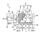
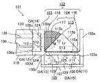
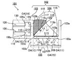
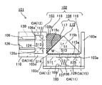
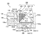
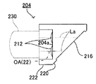
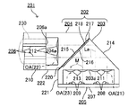
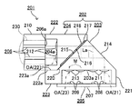
- 1 is a schematic configuration diagram showing an embodiment of an optical module according to the first invention.
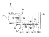
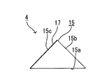
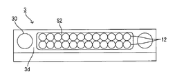
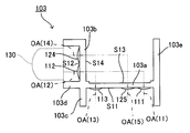
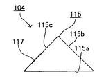
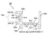
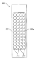
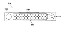
- 1 is a longitudinal sectional view showing a lens array body in an embodiment of a lens array according to the first invention; The longitudinal cross-sectional view which shows an optical path control member in embodiment of the lens array which concerns on 1st invention Left side view of FIG. Bottom view of FIG.
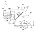
- the longitudinal section showing the 2nd lens member in the embodiment of the lens array concerning the 3rd invention The bottom view of FIG. Left side view of FIG.
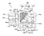
- the figure which shows the 1st modification of 3rd invention The figure which shows the 2nd modification of 3rd invention.
- FIG. 1 is a schematic configuration diagram showing an outline of the optical module 1 in the present embodiment together with a longitudinal sectional view of the lens array 2 in the present embodiment.
- FIG. 2 is a longitudinal sectional view of the lens array body 3 constituting the lens array 2.
- FIG. 3 is a longitudinal sectional view of the optical path control member 4 constituting the lens array 2 together with the lens array body 3.
- FIG. 4 is a left side view of FIG.
- FIG. 5 is a bottom view of FIG.
- the lens array 2 in the present embodiment is arranged between a photoelectric conversion device 5 and an optical fiber 6 as an optical transmission body.
- the photoelectric conversion device 5 has a plurality of light emitting elements 8 that emit (emit) laser light La on a surface facing the lens array 2 in the semiconductor substrate 7 in a direction perpendicular to the surface (upward in FIG. 1).
- These light emitting elements 8 constitute the VCSEL (Vertical Cavity Surface Emitting Laser) described above.
- the emission direction of the laser light La from each light emitting element 8 corresponds to the third direction in the present invention.
- a plurality of light emitting elements 8 (12 in the present embodiment) are arranged at an equal pitch along the direction perpendicular to the paper surface in FIG. 1 as the predetermined first direction, thereby forming a row of the light emitting elements 8.
- Such a row of light emitting elements 8 is formed so as to be juxtaposed in a plurality of rows (two rows in this embodiment) along the horizontal direction in FIG. 1 as the predetermined second direction.
- the number of the light emitting elements 8 is the same between the columns of the light emitting elements 8, and the positions in the alignment direction of the light emitting elements 8 are aligned between the columns (one).
- the present invention is not limited to such a configuration.
- the photoelectric conversion device 5 is a surface facing the lens array 2 in the semiconductor substrate 7, which is on the second direction side with respect to the light emitting elements 8 in a plurality of rows and on the optical transmission body side.
- a light emitting element 8 that receives monitor light M for monitoring the output (for example, intensity and light quantity) of the laser light La emitted from the plurality of rows of light emitting elements 8 at a position near the left in FIG.
- the same number of light receiving elements 9 are provided.
- the light receiving elements 9 form a row of the light receiving elements 9 by being aligned at equal pitches along the direction perpendicular to the paper surface in FIG. 1.
- the rows are formed so that a plurality of rows (two rows) are juxtaposed along the horizontal direction in FIG.
- the light receiving elements 9 in each column are optically corresponding to the columns of the light emitting elements 8 (which are in a relationship of monitoring light). The positions in the alignment direction coincide with each other.
- the light receiving elements 9 in the first column counted from the left are optically associated with the light emitting elements 8 in the first column counted from the right, and the second column from the right.
- the light receiving elements 9 in the second column from the left optically correspond to the light emitting elements 8.
- the light receiving element 9 may be a photo detector.
- the photoelectric conversion device 5 is connected to a control circuit for controlling the output of the laser light La emitted from the light emitting element 8 based on the intensity and the light amount of the monitor light M received by the light receiving element 9.
- a control circuit for controlling the output of the laser light La emitted from the light emitting element 8 based on the intensity and the light amount of the monitor light M received by the light receiving element 9.
- a photoelectric conversion device 5 is arranged to face the lens array 2 in a state where the semiconductor substrate 7 is in contact with the lens array 2.
- the photoelectric conversion device 5 constitutes the optical module 1 together with the lens array 2 by being attached to the lens array 2 by a known fixing means (not shown) such as a clamp spring.
- the same number of optical fibers 6 in the present embodiment as the light emitting elements 8 and the light receiving elements 9 are arranged, and a plurality (12) of optical fibers 6 are aligned along the direction perpendicular to the paper surface in FIG.
- the columns are arranged so that a plurality of columns (two columns) are juxtaposed along the vertical direction (third direction) in FIG.
- the optical fibers 6 and the light emitting elements 8 in the same order counted from one side in the alignment direction between the optical fibers 6 in the plurality of rows and the optically corresponding rows of light emitting elements 8 (in which light is coupled).
- the positions in the alignment direction of each other coincide with each other.
- the optical fibers 6 in the first row counted from the top optically correspond to the light emitting elements 8 in the second row from the right, and the optical fibers in the second row from the top.
- the sixth column optically corresponds to the light-emitting elements 8 in the first column from the right.
- the optical fibers 6 in each row are, for example, multimode optical fibers 6 having the same dimensions, and the end face 6a side portion is a multi-fiber batch type optical connector 10 such as an MT (Mechanically Transferable) connector. Is held in. As shown in FIG. 1, such a plurality of rows of optical fibers 6, with the end surface on the lens array 2 side of the optical connector 10 in contact with the lens array 2, known fixing means (not shown) (for example, The lens array 2 is attached by a clamp spring or the like.
- MT Mechanismically Transferable
- the lens array 2 is disposed between the photoelectric conversion device 5 and the optical fiber 6 and optically connects the plurality of rows of light emitting elements 8 and the end faces 6a of the plurality of rows of optical fibers 6 corresponding thereto. It is supposed to be combined with.
- the lens array 2 has a lens array body 3 made of a translucent material (for example, a resin material).
- the outer shape is formed in a substantially box shape.
- the lens array body 3 has a first plate-like portion 3 a having a planar rectangular horizontal plate shape, and the first plate-like portion 3 a.
- a predetermined width in the horizontal direction, a predetermined depth in the vertical direction on the drawing, a predetermined thickness in the vertical direction, and the photoelectric conversion device 5 are faced from above.
- FIGS. 1 the lens array body 3 made of a translucent material (for example, a resin material).
- the outer shape is formed in a substantially box shape.
- the lens array body 3 has a first plate-like portion 3 a having a planar rectangular horizontal plate shape, and the first plate-like portion 3 a.
- a predetermined width in the horizontal direction, a predetermined depth in the vertical direction on the drawing, a predetermined thickness in the vertical direction, and the photoelectric conversion device 5 are faced from above.
- the lens array body 3 is a plane that is connected to the left end portion of the first plate-like portion 3 a on the second direction side as the end portion on the optical transmission body side.
- a rectangular plate-like second plate-like portion 3b is provided, and the second plate-like portion 3b is formed to have the same depth as the first plate-like portion 3a.
- the second plate-like portion 3b extends vertically upward from the left end portion of the first plate-like portion 3a so as to be orthogonal to the first plate-like portion 3a. Since it is integral with the plate-like portion 3a, it is naturally formed with the same refractive index as that of the first plate-like portion 3a. Further, the second plate-like portion 3b faces the end face 6a of the optical fibers 6 in a plurality of rows from the right side in FIGS.
- the lower end surface (plane) of the first plate-like portion 3a in the lens array main body 3 is a first surface S1 that faces the photoelectric conversion device 5, and the first surface S1 includes the first surface S1 shown in FIG.
- the same number of planar circular first lens surfaces (convex lens surfaces) 11 as the light emitting elements 8 are formed.
- the first lens surfaces 11 are arranged in a plurality (12) at equal pitches along the direction perpendicular to the paper surface in FIG. 2 (vertical direction in FIG. 5).
- the first lens surface 11 is formed in a row, and such a row is formed so that a plurality of rows (two rows) are juxtaposed along the horizontal direction in FIGS. 2 and 5.
- the first lens surface 11 of each row is formed with the same size and is counted from one side in the alignment direction with the row of light-emitting elements 8 optically corresponding (with light incident thereon).
- the positions of the first lens surface 11 and the light emitting elements 8 in the alignment direction coincide with each other.
- the positions in the alignment direction of the light emitting elements 8 are aligned between the respective columns of the light emitting elements 8, such coincidence of positions with the columns of the light emitting elements 8 that are not optically compatible with each other. It is also established between the first lens surface 11 and the row.
- the first lens surface 11 in the first row counted from the right optically corresponds to the light emitting elements 8 in the first row counted from the right facing these from the lower side.
- the first lens surface 11 in the second row from the right optically corresponds to the light emitting elements 8 in the second row from the right facing these from the lower side.
- the first lens surfaces 11 adjacent to each other in the alignment direction (longitudinal direction) and the parallel direction (lateral direction) are formed in an adjacent state in which their peripheral ends are in contact with each other. May be.
- the optical axis OA (1) of each first lens surface 11 has a laser beam La emitted from each light emitting element 8 optically corresponding to each first lens surface 11 respectively. It is desirable to coincide with the central axis. More preferably, the optical axis OA (1) of each first lens surface 11 is orthogonal to the first surface S1.
- the laser light La emitted for each column of the optically corresponding light emitting elements 8 is incident on the first lens surface 11 of each column. More specifically, any one of the first lens surfaces 11 belonging to the row of the first lens surfaces 11 has an alignment direction among the light emitting devices 8 belonging to the optically corresponding row of the light emitting devices 8. The light emitted from one light-emitting element 8 in the same order as that of any one first lens surface 11 from one side of the light enters. Then, the first lens surface 11 in each row advances the laser beam La for each light emitting element 8 in each row to the inside (upward) of the first plate-like portion 3a.
- the first lens surface 11 in each row may collimate or converge the laser light La for each light emitting element 8 in each row that has entered.
- the laser light La may be diverged by forming the first lens surface 11 of each row as a concave lens surface.
- the left end surface (plane) of the second plate-like portion 3b is a second surface S2 facing the end surface 6a of the optical fiber 6, and this second surface S2 is shown in FIGS.
- the same number of planar second lens surfaces (convex lens surfaces) 12 as the light emitting elements 8 are formed.
- the second lens surface 12 is arranged in a plurality (12) at equal pitches along the paper surface vertical direction in FIG. 2 (lateral direction in FIG. 4).
- the second lens surface 12 is formed in a row, and such a row is formed so that a plurality of rows (two rows) are juxtaposed along the vertical direction in FIGS. 2 and 4.
- the second lens surface 12 of each row is formed with the same size and is counted from one side in the alignment direction with the row of light-emitting elements 8 optically corresponding (with light incident thereon).
- the positions of the second lens surface 12 and the light emitting elements 8 in the same order in the alignment direction are coincident with each other.
- the positions in the alignment direction of the light emitting elements 8 are aligned between the respective columns of the light emitting elements 8, such coincidence of positions with the columns of the light emitting elements 8 that are not optically compatible with each other. This also holds between the second lens surface 12 and the row.
- the second lens surface 12 in the first row counted from the top optically corresponds to the light emitting elements 8 in the second row counted from the right, and the second lens surface 12 from the top is second.
- the second lens surface 12 in the row optically corresponds to the light emitting elements 8 in the first row from the right.
- the second lens surfaces 12 that are adjacent to each other in the alignment direction and the parallel direction may be formed in an adjacent state in which their peripheral ends are in contact with each other.
- the optical axis OA (2) of each second lens surface 12 is optically corresponding to each second lens surface 12 (in a relationship for coupling light). It is desirable to coincide with the central axis of the end face 6a of the fiber 6. More preferably, the optical axis OA (2) of each second lens surface 12 is orthogonal to the second surface S2.
- the laser light La emitted for each column of the optically corresponding light-emitting elements 8 is applied to the second lens surface 12 of each column.
- the light enters after passing through the first lens surface 11 and the optical path (details will be described later) of the lens array 2 thereafter.
- any one second lens surface 12 belonging to the row of second lens surfaces 12 has an alignment direction among the light emitting devices 8 belonging to the optically corresponding row of light emitting devices 8.
- the light emitted from the light emitting elements 8 in the same order as that of any one of the second lens surfaces 12 from one side of the light enters through the first lens surface 11 in the same order.
- the central axis of the laser beam La for each light emitting element 8 in each column coincides with the optical axis OA (2) of the second lens surface 12 in each corresponding column. Then, the second lens surface 12 in each row converges the laser light La for each light emitting element 8 in each row to converge the optical fibers 6 in each row corresponding to the second lens surface 12 in each row. The light is emitted toward the end surface 6a.
- the light emitting elements 8 in each row and the end surfaces 6a of the optical fibers 6 in each row are optically coupled via the first lens surface 11 in each row and the second lens surface 12 in each row. It has become so.
- Lens surface (convex lens surface) 13 is formed on the first surface S1 and on the left side of the first lens surface 11 in each row.
- Lens surface (convex lens surface) 13 is formed on the first surface S1 and on the left side of the first lens surface 11 in each row.
- Lens surface (convex lens surface) 13 is formed on the first surface S1 and on the left side of the first lens surface 11 in each row.
- Lens surface (convex lens surface) 13 is formed on the first surface S1 and on the left side of the first lens surface 11 in each row.
- a plurality of (12) third lens surfaces 13 are arranged at equal pitches along the direction perpendicular to the paper surface in FIG. 2 (the vertical direction in FIG. 5).
- the third lens surface 13 is formed in a row, and such a row is formed so that a plurality of rows (two rows) are juxtaposed along the horizontal direction in FIGS. 2 and 5.
- the third lens surface 13 of each row is formed with the same size and is counted from one side in the alignment direction with the row of light-emitting elements 8 optically corresponding (with light incident thereon).
- the positions of the third lens surface 13 and the light emitting elements 8 in the same order in the alignment direction are coincident with each other.
- the positions in the alignment direction of the light emitting elements 8 are aligned between the respective columns of the light emitting elements 8, such coincidence of positions with the columns of the light emitting elements 8 that are not optically compatible This is also established between the third lens surface 13 and the row.
- the third lens surface 13 in the first row counted from the left optically corresponds to the light emitting elements 8 in the first row counted from the right, and the second lens surface 13 from the left.
- the third lens surface 13 in the row optically corresponds to the light emitting elements 8 in the second row from the right.
- the third lens surfaces 13 that are adjacent to each other in the alignment direction and the parallel direction may be formed in an adjacent state in which their peripheral ends are in contact with each other.
- the optical axis OA (3) of the third lens surface 13 in each row optically corresponds to the third lens surface 13 in each row (has a relationship for coupling light), and the light receiving element in each row. It is desirable to coincide with the central axis of the light receiving surface 9. More preferably, the optical axis OA (3) of the third lens surface 13 in each row is orthogonal to the first surface S1.
- the third lens surfaces 13 in each row correspond to the third lens surfaces 13 in each row from the inner side (upper side) of the first plate-like portion 3a.
- the monitor light M for each light emitting element 8 in the column enters.
- the third lens surface 13 in each row converges the incident monitor light M for each light emitting element 8 in each row, and receives the light in each row optically corresponding to the third lens surface 13 in each row.
- the light is emitted toward the element 9.
- the means for generating the monitor light M will be described later.
- the upper end surface of the first plate-like portion 3 a is formed with a recessed plane (counterbore surface) slightly recessed downward, and this recessed plane is
- the third plate S3 is a third surface S3 opposite to the first surface S1 in the first plate-like portion 3a.
- a gap is provided at a position near the upper portion of the third surface S3 above the third surface S3 (on the third direction side and opposite to the photoelectric conversion device 5).
- the optical path control member 4 is a prism having a longitudinal section triangle shape (triangular prism shape) made of a translucent material (for example, a resin material).
- This prism 15 forms an optical path of the laser light La for each light emitting element 8 in each row after entering the first lens surface 11 in each row.
- the prism 15 has a first prism surface 15a that forms a part (bottom surface) of the surface of the prism 15, and the first prism surface 15a is a third prism surface. It faces the surface S3 from above.
- the lateral width of the first prism surface 15a is substantially the same as the lateral width of the first plate-like portion 3a.
- the gap between the first prism surface 15a and the third surface S3 is a space formed by the third surface S3 being a concave surface, and in this space Is filled with a first filler 16 made of a translucent adhesive.
- the prism 15 is bonded to the lens array body 3 by using the adhesive force of the first filler 16.
- a thermosetting resin, an ultraviolet curable resin, or the like can be used.
- Laser light La for each of the light emitting elements 8 in each column of light enters from below (third direction).
- the first prism surface 15 a transmits the incident laser light La for each light emitting element 8 and travels it onto the optical path inside the prism 15.
- the prism 15 has a second prism surface 15b that forms a part of the surface (right slope), and the second prism surface 15b is a lower end portion thereof. And connected to the right end portion of the first prism surface 15a, and toward the second plate-like portion 3b side (left side) with increasing distance from the first prism surface 15a with respect to the first prism surface 15a. It has a predetermined inclination angle that inclines.
- the second prism surface 15b has a laser for each light emitting element 8 in each row after entering the first prism surface 15a and traveling on the optical path inside the prism 15.
- Light La is incident internally from below at an incident angle greater than the critical angle. Then, the second prism surface 15b totally reflects the laser light La for each light emitting element 8 in each column incident on the second prism surface 15b (to the left) in each column.
- the prism 15 has a third prism surface 15c forming a part of the surface (left slope), and the third prism surface 15c is a lower end portion thereof. Are connected to the left end portion of the first prism surface 15a, and are connected to the upper end portion of the second prism surface 15b at the upper end portion.
- the third prism surface 15c is opposite to the second plate-like portion 3b (on the right side as the first prism surface 15a is separated from the first prism surface 15a). ) To have a predetermined inclination angle.
- the third prism surface 15c is totally reflected by the second prism surface 15b and travels on the optical path inside the prism 15 for each light emitting element 8 in each column.
- Laser light La is incident on the inside from the right.
- the optical path control member 4 further has a thin reflection / transmission layer 17 on the third prism surface 15 c as shown in FIGS. 1 and 3.
- the reflective / transmissive layer 17, Ni, a plurality of dielectric monolayer film or a mutually dielectric constant consists of a single metal are different, such as Cr or Al (e.g., TiO 2 and SiO 2) by stacking alternately
- the obtained dielectric multilayer film may be formed by coating on the third prism surface 15c.
- a known coating technique such as Inconel vapor deposition can be used for coating.
- the reflection / transmission layer 17 can be formed to an extremely thin thickness of, for example, 1 ⁇ m or less.
- the laser light La for each light emitting element 8 in each row incident on the third prism surface 15c is immediately incident on the reflection / transmission layer 17 as described above.
- the reflection / transmission layer 17 uses the incident laser light La for each light-emitting element 8 in each column at a predetermined reflectivity and the monitor light for each light-emitting element 8 in each column corresponding to the light-emitting element 8 in each column.
- M is reflected toward the third lens surface 13 side (downward) of each row corresponding to each monitor light M, and at the predetermined transmittance, on the second lens surface 12 side (left side) of each row. Make it transparent.
- the reflectivity / transmittance of the reflection / transmission layer 17 is limited to the material of the reflection / transmission layer 17 as long as the monitor light M can be obtained with an amount of light that is considered sufficient for monitoring the output of the laser beam La. It is possible to set a desired value according to the thickness or the like. For example, when the reflection / transmission layer 17 is formed of the above-described single layer film, depending on the thickness, the reflection / transmission layer 17 has a reflectance of 20% and a transmittance of 60% (absorption rate of 20%). ). For example, when the reflection / transmission layer 17 is formed of the above-described dielectric multilayer film, the reflection / transmission layer 17 has a reflectance of 10% and a transmittance of 90%, depending on the thickness and the number of layers. %.
- the monitor light M for each light emitting element 8 in each column reflected by the reflection / transmission layer 17 travels on the optical path inside the prism 15, and the first prism surface 15 a and the first filler. 16 and the first plate-like portion 3a are sequentially transmitted and then internally incident on the third lens surface 13 of each corresponding row, and the light receiving elements of each row corresponding to these from the third lens surface 13 of each row It is emitted toward 9 respectively.
- thermosetting property between the reflection / transmission layer 17 and the fourth surface S4 (right end surface) opposite to the second surface S2 in the second plate-like portion 3b.
- a second filler 18 made of a translucent adhesive such as resin or ultraviolet curable resin is filled. Therefore, the prism 15 is more stably bonded to the lens array body 3 by using the adhesive force of the second filler 18 as well as the first filler 16.
- the second filler 18 has a refractive index difference with the prism 15 equal to or less than a predetermined value. This difference in refractive index is preferably 0.01 or less, and more preferably 0.005 or less.
- OKP4HT manufactured by Osaka Gas Chemical Co.
- the second filler 18 is formed of EA-0200 manufactured by Osaka Gas Chemical Co. as UV curable resin. Also good.
- the refractive indexes of the prism 15 and the second filler 18 can be 1.61 for light having a wavelength of 850 nm.
- the laser beam La for each light emitting element 8 in each column transmitted by the reflection / transmission layer 17 immediately enters the second filler 18.
- the incident direction of the laser light La for each light emitting element 8 in each column with respect to the second filler 18 is regarded as the same as the incident direction of the laser light La for each light emitting element 8 in each column with respect to the reflection / transmission layer 17. be able to. This is because the reflection / transmission layer 17 is very thin and the refraction of the laser beam La in this layer 17 can be ignored.
- the laser light La for each light emitting element 8 in each row incident on the second filler 18 travels on the optical path inside the second filler 18 toward the second lens surface 12 side in each row. To do.
- each laser beam La for each light-emitting element 8 in each column is incident on the second filler 18. No refraction occurs in the light La. Then, the laser light La for each of the light emitting elements 8 in each row that has traveled on the optical path inside the second filler 18 passes through the second plate-like portion 3b and reaches the second lens surface 12 in each row. Internally incident and emitted by the second lens surface 12 in each row toward the end surface 6a of the optical fiber 6 in each row corresponding thereto.
- the laser beam La for each of the light emitting elements 8 in each column incident on the first lens surface 11 in each column is totally reflected on the second prism surface 15b and then the reflection / transmission layer 17.
- the light can be dispersed on the second lens surface 12 side of each row and the third lens surface 13 side of each row.
- the laser light La for each light emitting element 8 in each column split (transmitted) to the second lens surface 12 side in each column is transmitted to the end surface of the optical fiber 6 in each column by the second lens surface 12 in each column.
- the monitor light M for each light-emitting element 8 in each row which is emitted to the 6a side and dispersed (reflected) with sufficient reflectance on the third lens surface 13 side in each row, is supplied to the third lens in each row.
- the light can be emitted to the light receiving element 9 side of each row by the surface 13.
- the refractive index difference between the prism 15 and the second filler 18 is formed to be equal to or smaller than a predetermined value. Since linearity with the optical path inside the material 18 can be ensured, the laser light La incident on the second lens surface 12 in each row during product inspection is shifted from the center of each lens surface 12. When this is confirmed, it is possible to reduce the places that require dimensional adjustment to eliminate this, and thus contribute to facilitating manufacturing.
- the third surface S3 is formed so as to be orthogonal to the optical axis OA (1) of the first lens surface 11 of each row.
- the first prism surface 15a is arranged in parallel to the third surface S3.
- the laser light La for each light emitting element 8 in each column can be perpendicularly incident on the first filler 16 and the first prism surface 15a.
- a simple design in which the linearity of the optical path between the first lens surface 11 and the second prism surface 15b can be ensured can be performed, and the lens array body 3, the first filler 16 and the prism 15 can be performed. It is also possible to expand the degree of freedom in selecting the material (refractive index).
- the fourth surface S4 is formed so as to be orthogonal to the optical axis OA (2) of the second lens surface 12 of each row. Then, the laser light La for each light emitting element 8 in each column transmitted through the reflection / transmission layer 17 is vertically incident from the second filler 18 side.
- the simple design with which the linearity of the optical path before and behind 4th surface S4 was ensured can be performed, and also the lens array main body 3 and the 2nd filler 18 can be performed. It is also possible to increase the degree of freedom in selecting the material (refractive index).
- the inclination angle of the second prism surface 15b is the same with respect to the first prism surface 15a as a reference (0 °).
- the angle is 45 ° clockwise in the figure.
- the inclination angle of the third prism surface 15c is set to 45 ° counterclockwise in the drawings with respect to the first prism surface 15a. That is, the third prism surface 15c is perpendicular to the second prism surface 15b.
- the prism 15 can be formed in a right-angled isosceles triangle shape, the measurement of the dimensional accuracy of the prism 15 can be performed easily, and the handleability can be improved.
- the refractive index difference between the lens array body 3 and the first filler 16 may be formed to a predetermined value or less (for example, 0.01 or less (preferably 0.005 or less)). Good.
- the refractive index difference between the lens array main body 3 and the second filler 18 may be formed to be a predetermined value or less (for example, 0.01 or less (preferably 0.005 or less)). Good.
- first filler 16 and the second filler 18 may be the same.
- the lens array body 3 and the prism 15 may be made of the same material.
- cost can be reduced by unifying the materials.
- the lens array body 3 has a device-side circumferential convex portion 3 c for holding the photoelectric conversion device 5.
- the device-side circumferential convex portion 3c protrudes closer to the photoelectric conversion device 5 (lower side in FIG. 1) than the first surface S1 and the first lens surface 11 so as to surround the first surface S1 from four directions.
- the photoelectric conversion device 5 is held in contact with the front end surface (lower end surface). Note that the distal end surface of the device-side circumferential convex portion 3c is parallel to and flush with the first surface S1.
- the lens array body 3 has a fiber-side circumferential convex portion 3 d for holding the optical fiber 6.
- the fiber-side circumferential convex portion 3d protrudes to the optical fiber 6 side (left side in FIG. 1) from the second surface S2 and the second lens surface 12 so as to surround the second surface S2 from four directions.
- the optical fiber 6 is held in contact with the front end surface (left end surface).
- the distal end surface of the fiber-side circumferential convex portion 3d is parallel to and flush with the second surface S2.
- the device-side circumferential convex portion 3c and the photoelectric conversion device 5 are mechanically or optically engaged with each other to position the photoelectric conversion device 5 with respect to the lens array 2.
- the positioning means may be formed.
- positioning means a combination of a pin formed on one of the device-side circumferential convex portion 3c and the photoelectric conversion device 5 and a pin insertion hole or hole formed on the other, or a device-side circumferential shape Examples include an optically detectable mark formed at a predetermined position of the convex portion 3c and the photoelectric conversion device 5.
- positioning means pins and pins for positioning the optical fiber 6 with respect to the lens array 2 by mechanically or optically engaging the fiber side circumferential convex portion 3d and the optical fiber 6 (connector 10).
- a combination of holes / holes, optical marks, etc. may be formed.
- the lens array main body 3 is opposite to the second plate-like portion 3b and is connected to the right end portion of the first plate-like portion 3a in a perpendicular manner.
- a plate-like portion 3e is formed.
- the third plate-like portion 3e may be provided as necessary.
- the second filler 18 flows out onto the second prism surface 15 b at the boundary position between the second prism surface 15 b and the third prism surface 15 c. You may use what the wall part 20 for preventing was standingly arranged.
- the wall portion 20 dams the second filler 18, so that the second filler 18 has the second prism surface 15 b on the second filler 18. Can be reliably suppressed, so that the total reflection function of the second prism surface 15b can be appropriately ensured.
- the first prism surface 15a may be formed as a recessed surface instead of the third surface S3 as a recessed surface.
- the second filler 18 is formed on the edge of the third prism surface 15 c as the prism 15.
- step-difference part 21 for preventing the outflow on the prism surface 15b may be used.
- the convex stepped portion 21 is formed in a substantially U-shape so as to surround the reflection / transmission layer 17 and in the surface normal direction of the third prism surface 15 c relative to the reflection / transmission layer 17. It is formed so as to protrude by a predetermined dimension.
- the second filling material 18 can be easily accumulated on the reflection / transmission layer 17 by the convex stepped portion 21, the second filling material 18 has the second prism surface 15 b on the second filling material 18. Can be effectively suppressed, and the total reflection function of the second prism surface 15b can be appropriately ensured. (Fourth modification)
- FIG. 9 a configuration corresponding to not only transmission of an optical signal but also reception of an optical signal may be adopted. That is, as shown in FIG. 9, a plurality of receiving optical fibers 6 'are arranged in the vicinity of the lower part of each row of optical fibers 6 along the direction perpendicular to the paper surface. Further, as shown in FIG. 9, at the position facing the end face 6a ′ of the receiving optical fiber 6 ′ on the second surface S2, the same number of receiving fourth lens surfaces as the receiving optical fiber 6 ′ are provided. 24 are formed in alignment along the direction perpendicular to the paper surface. Further, as shown in FIG.
- a portion in a predetermined range on the lower end side of the third prism surface 15 c is an extension portion extended from the lower end portion 17 a of the reflection / transmission layer 17.
- the reflective / transmissive layer 17 is not formed on the top.
- the same number of reception fifth lens surfaces 25 as the reception optical fibers 6 ' are aligned and formed along the direction perpendicular to the paper surface.
- the photoelectric conversion device 5 includes the same number of receiving light receiving elements 27 as the receiving optical fibers 6 ′.
- the laser beam La ′ for reception emitted from the end surface 6a ′ of the optical fiber 6 ′ for reception is converged by the fourth lens surface 24, and the second plate-like portion 3b, After sequentially transmitting (straight forward) through the second filler 18 and the extension of the third prism surface 15 c, the second prism surface 15 b is totally reflected toward the fifth lens surface 25, and is reflected on the fifth lens surface 25. The light is converged and properly coupled to the light receiving element 27 for reception.
- the light emitting element 8, the light receiving element 9, and the first to third lens surfaces 11 to 13 may be provided in three or more rows.
- the fourth and fifth lens surfaces 24 and 25 may be provided in two or more rows.
- the present invention can be effectively applied to an optical transmission body other than an optical fiber such as an optical waveguide.
- FIG. 10 is a schematic configuration diagram showing an outline of the optical module 101 in the embodiment of the second invention of the present application together with a longitudinal sectional view of the lens array 102 in the present embodiment.
- FIG. 11 is a longitudinal sectional view of the lens array main body 103 constituting the lens array 102.
- FIG. 12 is a longitudinal sectional view of the optical path control member 104 constituting the lens array 102 together with the lens array main body 103.
- FIG. 13 is a left side view of FIG.
- FIG. 14 is a bottom view of FIG.
- the lens array 102 in this embodiment includes a first photoelectric conversion device 105 for optical transmission / reception, an optical fiber 106 for optical transmission as an optical transmission body, and an optical fiber 126 for optical reception. It is arranged between them.
- the first photoelectric conversion device 105 has a surface facing the lens array 102 in the semiconductor substrate 107, and a laser beam Lt (only the center light of the luminous flux) in a direction perpendicular to the surface (upward direction in FIG. 10).
- the light emitting elements 108 constitute a VCSEL (vertical cavity surface emitting laser) as described above.
- the emission direction of the laser light Lt from each light emitting element 108 corresponds to the third direction in the present invention.
- the light emitting elements 108 are arranged at an equal pitch (12 in the present embodiment) along the direction perpendicular to the paper surface in FIG. 10 as the predetermined first direction, whereby a row (one row) of the light emitting elements 108 is formed. ). Furthermore, as shown in FIG.
- the first photoelectric conversion device 105 is a surface facing the lens array 102 in the semiconductor substrate 107, and is on the second direction side with respect to the row of the light emitting elements 108 and transmits light.
- a monitor light M (only the center light is shown) for monitoring the output (for example, intensity and light amount) of the laser light Lt emitted from each of the plurality of light emitting elements 108 at the left position in FIG. 10 as the body side position.
- the number of first light receiving elements 109 is the same as the number of light emitting elements 108 that receive light. Similar to the light emitting element 108, the first light receiving elements 109 are arranged at an equal pitch along the direction perpendicular to the paper surface in FIG.
- the first light receiving element 109 may be a photodetector.
- the first photoelectric conversion device 105 is a surface facing the lens array 102 in the semiconductor substrate 107, and is between the column of the light emitting elements 108 and the column of the first light receiving elements 109.
- the light receiving element 129 is provided.
- the second light receiving elements 129 are arranged at an equal pitch along the direction perpendicular to the paper surface in FIG. 10, thereby forming a row (one row) of the second light receiving elements 129.
- the second light receiving element 129 may be a photo detector.
- the first photoelectric conversion device 105 receives the output of the laser light Lt emitted from the light emitting element 108 based on the intensity and light quantity of the monitor light M received by the first light receiving element 109.
- a control circuit for controlling is connected. As shown in FIG. 10, such a first photoelectric conversion device 105 is arranged to face the lens array 102 in a state where the semiconductor substrate 107 is in contact with the lens array 102.
- the first photoelectric conversion device 105 is attached to the lens array 102 by a known fixing means (not shown) such as a clamp spring, so that the optical module 101 is configured together with the lens array 102. .
- the same number of optical fibers 106 for light transmission in the present embodiment as the light emitting elements 108 and the first light receiving elements 109 are arranged and aligned along the direction perpendicular to the paper surface in FIG.
- the plurality of optical fibers 106 for optical transmission coincide with each other in the alignment direction with the light emitting elements 108 in the same order as counted from one of the alignment directions.
- the number of optical fibers 126 for light reception in this embodiment is the same as the number of second light receiving elements 129 (in this embodiment, the same number of light emitting elements 108, first light receiving elements 109, and optical fibers 106 for light transmission). And arranged in alignment along the direction perpendicular to the paper surface in FIG.
- the plurality of optical fibers 126 for receiving light coincide with each other in the alignment direction with the second light receiving elements 129 in the same order as counted from one of the alignment directions.
- the row of optical fibers 126 for receiving light is arranged above the row of optical fibers 106 for transmitting light.
- the optical fibers 106 and 126 in each row are, for example, multimode optical fibers 106 and 126 of the same size, and the end surfaces 106a and 126a side portions are multi-cores such as MT (Mechanically-Transferable) connectors. It is held in the collective optical connector 110. As shown in FIG.
- the optical fibers 106 and 126 in each row have known fixing means (not shown) in a state where the end surface on the lens array 102 side of the optical connector 110 is in contact with the lens array 102.
- it is attached to the lens array 102 by a clamp spring or the like.
- the lens array 102 is arranged between the first photoelectric conversion device 105 and the optical fibers 106 and 126 for optical transmission and reception, and a plurality of light emitting elements for optical transmission. 108 and the end faces 106a of the plurality of optical fibers 106 for optical transmission are optically coupled, and the end faces 126a of the plurality of optical fibers 126 for optical reception and the plurality of second light receiving elements 129 are used for optical reception. Are optically coupled.
- the lens array 102 has a lens array body 103 made of a light-transmitting material (for example, a resin material).
- the outer shape is formed in a substantially box shape.
- the lens array main body 103 has a first plate-like portion 103a having a planar rectangular horizontal plate shape, and the first plate-like portion 103a.
- a predetermined width in the horizontal direction, a predetermined depth in the vertical direction on the paper surface, a predetermined thickness in the vertical direction, and the first photoelectric conversion device 105 are faced from above. Yes.
- the lens array main body 103 has a third direction from the left end as the end on the second transmission direction side of the first plate-shaped portion 103a on the optical transmission body side.
- a second plate portion 103b having a vertical plate shape extending in a right angle toward the upper side is provided.
- the second plate-like portion 103b has the same depth as that of the first plate-like portion 103a and is integrally formed with the first plate-like portion 103a. 103a and the same refractive index.
- the second plate-like portion 103b faces the end faces 106a and 126a of the optical fibers 106 and 126 for light transmission and light reception from the right side in FIGS.
- the lower end surface (plane) of the first plate-like portion 103a in such a lens array main body 103 is a first surface S1 that faces the first photoelectric conversion device 105, and the first surface S1 includes the first surface S1.
- the same number of planar circular first lens surfaces (convex lens surfaces) 111 as the light emitting elements 108 are formed.
- the first lens surface 111 is aligned and formed at an equal pitch along the direction perpendicular to the paper surface in FIG. 11 (the vertical direction in FIG. 14).
- a line (one line) of the lens surface 111 is formed.
- the positions of the plurality of first lens surfaces 111 in the alignment direction coincide with each other with the light emitting elements 108 in the same order as counted from one of the alignment directions.
- the first lens surfaces 111 that are adjacent to each other may be formed in an adjacent state in which their peripheral ends are in contact with each other.
- the laser light Lt emitted for each of the plurality of light emitting elements 108 is incident on the plurality of first lens surfaces 111. More specifically, one arbitrary first lens surface 111 has one of the plurality of light emitting elements 108 in the same order as the arbitrary first lens surface 111 counted from one of the alignment directions. Light emitted from the light emitting element 108 enters. Each first lens surface 111 advances the laser beam Lt for each incident light emitting element 108 to the inside (upward) of the first plate-like portion 103a. Each first lens surface 111 may collimate or converge the incident laser light Lt for each light emitting element 108. Alternatively, the laser light Lt may be diverged by forming each first lens surface 111 as a concave lens surface.
- the left end surface (plane) of the second plate-like portion 103b is a second surface S12 that faces the end surfaces 106a and 126a of the optical fibers 106 and 126 for optical transmission and reception.
- the same number of planar circular second lens surfaces (convex lens surfaces) 112 as the light emitting elements 108 are formed on the surface S ⁇ b> 12.
- the second lens surfaces 112 are arranged at an equal pitch along the direction perpendicular to the paper surface in FIG. 11 (lateral direction in FIG. 13). A row (one row) of lens surfaces 112 is formed.
- the positions of the plurality of second lens surfaces 112 in the alignment direction are mutually coincident with the light emitting elements 108 in the same order as counted from one of the alignment directions.
- the second lens surfaces 112 adjacent to each other may be formed in an adjacent state in which their peripheral ends are in contact with each other.
- the laser light Lt emitted for each of the plurality of light emitting elements 108 is applied to the plurality of first lens surfaces 111 and the subsequent lens array 102 on the plurality of second lens surfaces 112. After passing through the optical path (details will be described later). More specifically, the light emitted from the light emitting elements 108 in the same order as that of any one second lens surface 112 counted from one side in the alignment direction is given to any one second lens surface 112 in the same order. The light enters through the first lens surface 111. At this time, it is desirable that the central axis of the laser light Lt for each light emitting element 108 coincides with the optical axis OA (12) of each second lens surface 112. Each second lens surface 112 converges the incident laser light Lt for each light emitting element 108 toward the end face 106 a of each optical fiber 106 for light transmission corresponding to each second lens surface 112. Respectively.
- each light emitting element 108 and the end face 106a of each optical fiber 106 for optical transmission are optically coupled via each first lens surface 111 and each second lens surface 112. ing.
- the same number of planar circular thirds as the light emitting elements 108 are provided on the first surface S11 and on the left side with respect to the row of the first lens surface 111.
- a lens surface (convex lens surface) 113 is formed on the first surface S11 and on the left side with respect to the row of the first lens surface 111.
- the third lens surface 113 is formed in an aligned manner along the direction perpendicular to the paper surface in FIG.
- a row (one row) of lens surfaces 113 is formed.
- the positions of the plurality of third lens surfaces 113 in the alignment direction coincide with each other with the light emitting elements 108 in the same order as counted from one of the alignment directions.
- FIG. 11 and FIG. 14 the third lens surface 113 is formed in an aligned manner along the direction perpendicular to the paper surface in FIG.
- a row (one row) of lens surfaces 113 is formed.
- the positions of the plurality of third lens surfaces 113 in the alignment direction coincide with each other with the light emitting
- the third lens surfaces 113 that are adjacent to each other may be formed in an adjacent state in which their peripheral ends are in contact with each other. Moreover, it is desirable that the optical axis OA (13) of each third lens surface 113 coincides with the central axis of the light receiving surface of each first light receiving element 109. More preferably, the optical axis OA (13) of each third lens surface 113 is orthogonal to the first surface S11.
- the monitor light M for each light emitting element 108 is incident on each third lens surface 113 from the inner side (upper side) of the first plate portion 103a. More specifically, the monitor light of the light emitting element 108 in the same order as that of any one third lens surface 113 counted from one side in the alignment direction is placed on the arbitrary one third lens surface 113 in the same order. The light enters through the first lens surface 111. Then, each third lens surface 113 converges the incident monitor light M for each light emitting element 108 toward each first light receiving element 109 optically corresponding to each third lens surface 113. Each is emitted.
- the means for generating the monitor light M will be described later.
- the fourth lens surface 124 is aligned and formed at an equal pitch along the direction perpendicular to the paper surface in FIG. 11 (lateral direction in FIG. 13). A line (one line) of the lens surface 124 is formed.
- the positions of the plurality of fourth lens surfaces 124 in the alignment direction coincide with each other with the optical fibers 126 for light reception in the same order as counted from one of the alignment directions.
- the fourth lens surfaces 124 that are adjacent to each other may be formed in an adjacent state in which their peripheral ends are in contact with each other. Further, such an adjacent state may be established between the second lens surface 112 as shown in FIG.
- the laser light Lr emitted for each of the plurality of optical fibers 126 for receiving light is incident on the plurality of fourth lens surfaces 124. More specifically, any one fourth lens surface 124 is the same as any one fourth lens surface 124 counted from one of the alignment directions of the plurality of optical fibers 126 for light reception. The outgoing light from the end face 126a of the one optical fiber 126 in the order enters. Then, each fourth lens surface 124 advances the laser beam Lr for each incident optical fiber 126 to the inside (right side) of the second plate portion 103b. In addition, each 4th lens surface 124 may collimate the laser beam Lr for each incident optical fiber 126, or may converge it. Alternatively, the laser light Lr may be diverged by forming the fourth lens surfaces 124 as concave lens surfaces.
- the first lens surface on the first surface S11 as a position between the row of the first lens surface 111 and the row of the third lens surface.
- the same number of planar circular fifth lens surfaces (convex lens surfaces) 125 as the number of optical fibers 126 for receiving light are formed.
- the fifth lens surface 125 is aligned and formed at an equal pitch along the paper surface vertical direction (the vertical direction in FIG. 14) in FIG. A line (one line) of lens surfaces 125 is formed.
- the plurality of fifth lens surfaces 125 coincide with each other in the alignment direction with the optical fibers 126 for light reception in the same order as counted from one of the alignment directions.
- the fifth lens surfaces 125 adjacent to each other may be formed in an adjacent state in which their peripheral ends are in contact with each other. Further, such an adjacent state may be established with the first lens surface 111 as shown in FIG.
- the laser light Lr emitted for each of the plurality of optical fibers 126 for light reception is transmitted to the plurality of fourth lens surfaces 124 and thereafter. It enters after passing through the optical path of the lens array 102 (details will be described later). More specifically, the light emitted from the optical fiber 126 for receiving light in the same order as that of any one fifth lens surface 125 counted from one side in the alignment direction is provided on any one fifth lens surface 125. However, the light enters through the fourth lens surface 124 in the same order.
- each optical fiber 126 coincides with the optical axis OA (15) of each fifth lens surface 125.
- Each of the fifth lens surfaces 125 converges the incident laser light Lr for each optical fiber 126 and emits it toward each of the second light receiving elements 129 corresponding to each of the fifth lens surfaces 125. .
- each optical fiber 126 for receiving light and each second light receiving element 129 are optically coupled via each fourth lens surface 124 and each fifth lens surface 125. It is like that.
- the upper end surface of the first plate-like portion 103a is formed with a concave plane (counterbore surface) that is slightly recessed downward.
- the first plate-like portion 103a is a third surface S13 opposite to the first surface S11.
- a gap near the upper portion of the third surface S13 is above the third surface S13 (on the third direction side and opposite to the first photoelectric conversion device 105).
- the optical path control member 104 described above is arranged so as to provide the above.
- the optical path control member 104 is a prism having a triangular section (triangular prism shape) made of a translucent material (for example, a resin material).
- the prism 115 includes an optical path of the laser light Lt for each light emitting element 108 after being incident on each first lens surface 111 and each light after being incident on each fourth lens surface 124.
- the optical path of the laser beam Lr for each fiber 126 is formed.
- the prism 115 has a first prism surface 115 a that forms a part (bottom surface) of the surface of the prism 115, and the first prism surface 115 a is a third prism surface. It faces the surface S13 from above.
- the lateral width of the first prism surface 115a is formed to be approximately the same as the lateral width of the first plate-like portion 103a.
- the gap between the first prism surface 115a and the third surface S13 is a space formed by the third surface S13 being a concave surface.
- the prism 115 is bonded to the lens array body 103 using the adhesive force of the first filler 116.
- the first filler 116 a thermosetting resin, an ultraviolet curable resin, or the like can be used.
- the first prism surface 115 a is incident on each first lens surface 111 and passes through the first plate-like portion 103 a and the first filler 116.
- Laser light Lt for each light emitting element 108 enters from below (third direction).
- the first prism surface 115 a transmits the incident laser light Lt for each of the light emitting elements 108, and advances it onto the optical path inside the prism 115.
- the laser beam Lr for each optical fiber 126 after entering the respective fourth lens surfaces 124 is internally incident on the first prism surface 115a from above. Then, the first prism surface 115a transmits the laser light Lr for each optical fiber 126 incident on the inside to each fifth lens surface 125 side.
- the laser light Lr for each optical fiber 126 transmitted in this way is transmitted through the first filler 116 and the first plate portion 103a and is incident on each fifth lens surface 125, The light is emitted toward the second light receiving elements 129 corresponding thereto by the fifth lens surface 125.
- the prism 115 has a second prism surface 115b that forms a part of the surface (right slope), and the second prism surface 115b is a lower end portion thereof. And connected to the right end portion of the first prism surface 115a, and toward the second plate-like portion 103b side (left side) as the distance from the first prism surface 115a increases with respect to the first prism surface 115a. It has a predetermined inclination angle that inclines.
- the second prism surface 115b has a laser beam Lt for each light emitting element 108 after entering the first prism surface 115a and traveling on the optical path inside the prism 115. However, it is incident internally from below at an incident angle larger than the critical angle.
- the second prism surface 115b totally reflects the laser light Lt for each light emitting element 108 incident on the second prism surface 115 toward the second lens surface 112 (left side).
- the second prism surface 115b has a laser beam Lr for each optical fiber 126 after being incident on each fourth lens surface 124 and before being incident on the first prism surface 115a. Is incident from the left at an incident angle greater than the critical angle.
- the second prism surface 115b totally reflects the laser light Lr for each optical fiber 126 incident therein to the first prism surface 115a.
- the laser beam Lr for each optical fiber 126 that has been totally reflected in this way is incident on the first prism surface 115a as described above.
- the prism 115 has a third prism surface 115c that forms a part of the surface (left slope), and the third prism surface 115c is the lower end of the third prism surface 115c.
- the third prism surface 115c is opposite to the second plate-like portion 103b (on the right side as the first prism surface 115a is separated from the first prism surface 115a). ) To have a predetermined inclination angle.
- the laser light for each light emitting element 108 after being totally reflected by the second prism surface 115b and traveling on the optical path inside the prism 115 is provided.
- Lt is incident internally from the right side.
- the third prism surface 115c has a laser beam for each optical fiber 126 after being incident on each fourth lens surface 124 and before being internally incident on the second prism surface 115b.
- Lr is incident from the left. The laser beam Lr for each optical fiber 126 thus incident passes through the third prism surface 115c and then internally enters the second prism surface 115b as described above.
- the optical path control member 104 further includes an incident position of the laser light Lt for each light emitting element 108 on the third prism surface 115c, as shown in FIGS.
- a thin reflection / transmission layer 117 is formed over a half (lower half) region on the first plate-like portion 103a side.
- the reflection / transmission layer 117 is formed by alternately laminating a single layer film made of a single metal such as Ni, Cr or Al or a plurality of dielectrics (for example, TiO 2 and SiO 2 ) having different dielectric constants.
- the obtained dielectric multilayer film may be formed by coating on the third prism surface 115c.
- a known coating technique such as Inconel vapor deposition can be used for coating.
- the reflection / transmission layer 117 can be formed to an extremely thin thickness of, for example, 1 ⁇ m or less.
- the laser light Lt for each light emitting element 108 incident on the incident position on the third prism surface 115c is immediately incident.
- the reflection / transmission layer 117 uses the incident laser light Lt for each light emitting element 108 as the monitor light M for each light emitting element 108 corresponding to each light emitting element 108 with a predetermined reflectance.
- the thickness of the reflection / transmission layer 117 is thin, the refraction of the laser light Lt transmitted through the reflection / transmission layer 117 can be ignored (considered as a straight transmission).
- the reflectivity / transmittance of the reflection / transmission layer 117 is limited to the material of the reflection / transmission layer 117 as long as the monitor light M can be obtained with an amount of light that is considered sufficient for monitoring the output of the laser beam Lt. It is possible to set a desired value according to the thickness or the like. For example, when the reflection / transmission layer 117 is formed of the above-described single-layer film, the reflection / transmission layer 117 has a reflectance of 20% and a transmittance of 60% (absorption rate of 20%), depending on the thickness.
- the reflection / transmission layer 117 when the reflection / transmission layer 117 is formed of the above-described dielectric multilayer film, the reflection / transmission layer 117 has a reflectance of 10% and a transmittance of 90%, depending on the thickness and the number of layers. %.
- the monitor light M for each light emitting element 108 reflected by the reflection / transmission layer 117 in this way travels on the optical path inside the prism 115, and the first prism surface 115a, the first filler 116, and After sequentially passing through the first plate-like portion 103a, it is incident on each corresponding third lens surface 113 and from each third lens surface 113 toward each corresponding first light receiving element 109. Emitted.
- thermosetting property is provided between the reflective / transmissive layer 117 and the fourth surface S4 (right end surface) opposite to the second surface S12 in the second plate-like portion 103b.
- a second filler 18 made of a translucent adhesive such as resin or ultraviolet curable resin is filled. Therefore, the prism 115 is more stably bonded to the lens array body 103 by using not only the first filler 116 but also the adhesive force of the second filler 18.
- the second filler 18 has a refractive index difference with the prism 115 of a predetermined value or less. This difference in refractive index is preferably 0.01 or less, and more preferably 0.005 or less.
- the second filler 18 is formed of EA-0200 manufactured by Osaka Gas Chemical Co. as UV curable resin. Also good.
- the refractive indexes of the prism 115 and the second filler 18 can both be 1.61 for light having a wavelength of 850 nm.
- the laser beam Lt for each light emitting element 108 transmitted by the reflection / transmission layer 117 is immediately incident on the second filler 18.
- the incident direction of the laser light Lt for each light emitting element 108 with respect to the second filler 18 can be regarded as the same as the incident direction of the laser light Lt for each light emitting element 108 with respect to the reflection / transmission layer 117. This is because the reflection / transmission layer 117 is very thin and the refraction of the laser light Lt in this layer 117 can be ignored.
- the laser light Lt for each light emitting element 108 incident on the second filler 118 travels on the optical path inside the second filler 118 toward the second lens surface 112 side.
- each laser light Lt for each light emitting element 108 enters the second filler 118, each laser light Lt There will be no refraction. Then, the laser light Lt for each light emitting element 108 that has traveled on the optical path inside the second filler 118 passes through the second plate portion 103b and enters the second lens surface 112 internally. Each of the second lens surfaces 112 emits the light toward the end surface 106a of the corresponding optical fiber 106 for optical transmission. Further, as shown in FIG.
- the second filler 118 contains laser light Lr for each optical fiber 126 after being incident on each fourth lens surface 124 and before being incident on the third prism surface 115c. Enters from the left. Then, the laser light Lr for each optical fiber 126 traveling on the optical path inside the second filler 118 is incident on the incident position on the third prism surface 115c as described above. At this time, since the difference in refractive index between the second filler 118 and the prism 115 is sufficiently small, each laser beam Lr is incident when the laser beam Lr for each optical fiber 126 enters the third prism surface 115c. There will be no refraction.
- the laser light Lt for each light emitting element 108 incident on each first lens surface 111 is totally reflected on the second prism surface 115b and then reflected / transmitted by the reflection / transmission layer 117.
- the light can be dispersed on the second lens surface 112 side and each third lens surface 113 side.
- the laser light Lt for each light emitting element 108 dispersed (transmitted) to each second lens surface 112 side is emitted to the end surface 106 a side of each optical fiber 106 for light transmission by each second lens surface 112.
- the monitor light M for each light emitting element 108 that is dispersed (reflected) with sufficient reflectivity on the side of each third lens surface 113 is caused to pass through each first light receiving element 109 by each third lens surface 113. Can be emitted to the side.
- the laser light Lr for each optical fiber 126 for receiving light incident on each fourth lens surface 124 is transmitted through the non-formation region of the reflection / transmission layer 117 on the third prism surface 115 c
- the second prism surface 115b can be totally reflected on the fifth lens surface 125 side, and can be emitted to the second light receiving element 129 side by the fifth lens surface 125.
- each light emitting element 108 for optical transmission and the end face 106a of each optical fiber 106 can be appropriately performed, monitor light can be obtained reliably and efficiently, and Optical coupling between the end face 126a of each optical fiber 126 for reception and each second light receiving element 129 can be performed appropriately. Further, by integrating the total reflection function (115b) and the spectral function (117) at positions close to each other on one member 115, a compact and easy design is possible.
- the optical transmission region and the optical reception region are not divided in the lens surface alignment direction, but are divided in a direction orthogonal to the lens surface alignment direction,
- the transmission optical path and the optical reception optical path can be selected depending on whether or not the reflection / transmission layer 117 is formed.
- the optical path for optical reception can be arranged outside the optical transmission component (reflection / transmission layer 117) by a simple method, a compact design and a simple design of the optical path for optical reception can be achieved while being multi-channel. It becomes possible.
- the refractive index difference between the prism 115 and the second filler 118 is a predetermined value or less, the optical path between the second prism surface 115b and the third prism surface 115c, and the second Since linearity with the optical path inside the filler 118 can be ensured, the laser light Lt incident on each second lens surface 112 during product inspection may be shifted from the center of each lens surface 112. When it is confirmed, it is possible to reduce the places that require dimensional adjustment to eliminate this, and thus contribute to facilitating manufacturing.
- the second light receiving element 129 is arranged between the light emitting element 108 and the first light receiving element 109.
- the fifth lens surface 125 is arranged at a position between the first lens surface 111 and the third lens surface 113.
- the second prism face 115b is set such that the total reflection position of the laser light Lt for each light emitting element 108 is closer to the first plate-like portion 103a than the total reflection position of the laser light Lr for each optical fiber 126.
- the third prism surface 115c is set such that the incident position of the laser light Lt for each light emitting element 108 is set closer to the first plate portion 103a than the incident position of the laser light Lr for each optical fiber 126. Yes. Further, the reflection / transmission layer 117 is formed on a partial region of the third prism surface 115c on the first plate-like portion 103a side, and the second lens surface 112 is arranged as a fourth lens. It is arranged at a position on the first plate-like portion 103a side with respect to the row of the surfaces 124.
- the second filler 118 is used for the laser light Lt for each light emitting element 108 for which the desired coupling efficiency with respect to the end face 106a of each optical fiber 106 for optical transmission is required with high accuracy. Since the optical path length inside the prism 115 excellent in optical stability based on the uniformity of density than the optical path length inside the second filler 118 can be designed to be longer than each other. The coupling efficiency with respect to the end face 106a of the optical fiber 106 can be secured stably.
- the third surface S13 is formed so as to be orthogonal to the optical axis OA (11) of each first lens surface 111.
- the first prism surface 115a is disposed in parallel to the third surface S13.
- the laser light Lt for each light emitting element 108 can be perpendicularly incident on the first filler 116 and the first prism surface 115a.
- a simple design in which the linearity of the optical path between the surface 111 and the second prism surface 115b is ensured can be performed, and the material of the lens array main body 103, the first filler 116, and the prism 115 (refraction). Rate)
- the degree of freedom of selection can be expanded.
- the fourth surface S14 includes the optical axis OA (12) of each second lens surface 112 and each fourth lens surface 124.
- the laser light Lt for each light emitting element 108 that is formed so as to be orthogonal to the optical axis OA (14) of the light and transmitted through the reflection / transmission layer 117 is perpendicularly incident from the second filler 118 side, and each fourth The laser light Lr for each optical fiber 126 that has entered the lens surface 124 is perpendicularly incident on the second filler 118.
- the inclination angle of the second prism surface 115b is the same with respect to the first prism surface 115a (0 °).
- the angle is 45 ° clockwise in the figure.
- the inclination angle of the third prism surface 115c is set to 45 ° counterclockwise in the drawings with respect to the first prism surface 115a. That is, the third prism surface 115c is perpendicular to the second prism surface 115b.
- the prism 115 can be formed in a right-angled isosceles triangle shape, the measurement of the dimensional accuracy of the prism 115 can be easily performed, and the handleability can be improved. Further, the total reflection angle of the laser light Lt for each light emitting element 108 on the second prism surface 115b, the total reflection angle of the laser light Lr for each optical fiber 126, and the laser for each light emitting element 108 in the reflection / transmission layer 117. Since the total reflection angle of the light Lr can be designed to be 90 °, the optical path design is further facilitated.
- the refractive index difference between the lens array main body 103 and the first filler 116 may be formed to be a predetermined value or less (for example, 0.01 or less (preferably 0.005 or less)). Good.
- the refractive index difference between the first filler 116 and the prism 115 may be formed to a predetermined value or less (for example, 0.01 or less (preferably 0.005 or less)).
- the refractive index difference between the lens array main body 103 and the second filler 118 may be formed to a predetermined value or less (for example, 0.01 or less (preferably 0.005 or less)). Good.
- first filler 116 and the second filler 118 may be the same.
- the lens array body 103 and the prism 115 may be made of the same material.
- cost can be reduced by unifying the materials.
- the lens array main body 103 has a device-side circumferential convex portion 103 c for holding the first photoelectric conversion device 105.
- the device-side circumferential convex portion 103c surrounds the first surface S11 from all sides, and is closer to the first photoelectric conversion device 105 (lower side in FIG. 10) than the first surface S11 and the first lens surface 111. ), And the first photoelectric conversion device 105 is held in contact with the front end surface (lower end surface). Note that the tip end surface of the device-side circumferential convex portion 103c is parallel to and flush with the first surface S11. As shown in FIGS.
- the lens array main body 103 has a fiber-side circumferential convex portion 103 d for holding the optical fibers 106 and 126.
- the fiber-side circumferential convex portion 103d surrounds the second surface S12 from four directions, and is closer to the optical fibers 106 and 126 than the second surface S12 and the second lens surface 112 (left side in FIG. 10).
- the optical fibers 106 and 126 are held in contact with each other at the front end surface (left end surface).
- the distal end surface of the fiber-side circumferential convex portion 103d is parallel to and flush with the second surface S12.
- the first photoelectric conversion device for the lens array 102 is mechanically or optically engaged with the device side circumferential convex portion 103c and the first photoelectric conversion device 105 (semiconductor substrate 107).
- Positioning means for positioning 105 may be formed.
- this positioning means a combination of a pin formed on one of the device-side circumferential convex portion 103c and the first photoelectric conversion device 105 and a pin insertion hole or hole formed on the other, a device Examples thereof include an optically detectable mark formed at a predetermined position of the side circumferential convex portion 103 c and the first photoelectric conversion device 105.
- positioning means for positioning the optical fiber 106 with respect to the lens array 102 by mechanically or optically engaging the fiber side circumferential convex portion 103d and the optical fibers 106 and 126 (connector 110). A combination of a pin and a hole / hole, an optical mark, or the like may be formed.
- FIG. 11 and FIG. 13 show a pin 130 formed on the fiber-side circumferential convex portion 103d as an example of the positioning means.
- the lens array main body 103 is a third one that is opposed to the second plate-like portion 103b and that is vertically connected to the right end portion of the first plate-like portion 103a. Plate-like portion 103e. You may make it provide this 3rd plate-shaped part 103e as needed.
- the prism 115 causes the second filler 118 to flow out onto the second prism surface 115b at the boundary position between the second prism surface 115b and the third prism surface 115c. You may use what the wall part 120 for preventing was standingly arranged.
- the wall portion 120 blocks the second filler 118, so that the second filler 118 has a surface on the second prism surface 115 b. Therefore, the total reflection function of the second prism surface 115b can be appropriately ensured.
- the first prism surface 115a may be formed as a recessed surface instead of the third surface S13 as a recessed surface.
- the filling space (gap) of the first filler 116 can be easily secured between the third surface S13 and the first prism surface 115a.
- the second filler 118 is formed on the edge of the third prism surface 115c as the prism 115.
- the convex stepped portion 121 is formed in a substantially U-shape so as to surround the reflection / transmission layer 117, and in the surface normal direction of the third prism surface 115 c with respect to the reflection / transmission layer 117. It is formed so as to protrude by a predetermined dimension.
- the second filler 118 can be easily accumulated on the third prism surface 115 c and the reflection / transmission layer 117 by the convex stepped portion 121, and thus the second filler 118. Can be effectively suppressed from flowing out onto the second prism surface 115b, and the total reflection function of the second prism surface 115b can be appropriately ensured. (Fourth modification)
- the above-described lens surfaces 111 to 113, 124, 125, the light emitting element 108, the light receiving elements 109, 129, the optical fibers 106, 126, and the reflection / transmission layer 117 are maintained with their respective optical performances.
- the layout may be changed as shown in FIG.
- the first photoelectric conversion device 105 includes a second light receiving element 129 in the right position with respect to the light emitting element 108 (on the second direction side). At a position opposite to the optical fibers 106 and 126). Accordingly, as shown in FIG. 18, the row of the fifth lens surface 125 is positioned to the right of the row of the first lens surface 111 (on the second direction side and the second plate shape). (Position opposite to the portion 103b). Further, as shown in FIG. 18, the second prism surface 115 b has a total reflection position of the laser light Lt for each light emitting element 108 that is first than the total reflection position of the laser light Lr for each optical fiber 126.
- the third prism surface 115c is set on the side opposite to the plate-like portion 103a (upward), and the incident position of the laser beam Lt for each light emitting element 108 is the incident position of the laser beam Lr for each optical fiber 126. Rather than the first plate-like portion 103a. Furthermore, as shown in FIG. 18, the reflection / transmission layer 117 is a part of the third prism surface 115c on a side opposite to the first plate portion 103a as a predetermined range in the present modification. (Upper half). Further, as shown in FIG. 18, the second lens surface 112 row is positioned above the fourth lens surface 124 (on the third direction side and opposite to the first plate-like portion 103a). Position).
- the optical path of the laser light Lt for each light emitting element 108 after the second prism surface 115b can be shortened. Even if an error in the above or an assembly occurs, the influence of the error on the coupling efficiency of the laser light Lt for each light emitting element 108 can be reduced.
- two rows of third lens surfaces 113 may be arranged on the first surface S11 so as to be adjacent to each other in the lateral direction (second direction).
- the lens array main body 103 of this modification has the first photoelectric conversion device 105 and the reflection / transmission layer 117 formed on the third prism surface 115c over a predetermined range.
- the lens array 102 and the optical module 101 for optical transmission / reception can be configured with the prism 115 and the optical fibers 106 and 126 for optical transmission and reception arranged.
- the lens array 102 shown in FIG. 20 is the same as the configuration shown in FIGS. 10 to 14 except that a third lens surface 113 that does not function optically is added in a row.
- a second photoelectric conversion device 135 dedicated to optical transmission and a reflection / transmission layer 117 are entirely formed on the third prism surface 115c.
- the lens array 102 ′ and the optical module 101 ′ dedicated to optical transmission can be configured in a state where the prisms 115 and the two optical fibers 106 for optical transmission are arranged.
- the second photoelectric conversion device 135 has the second light receiving element 129 at a position corresponding to the arrangement position of the row of the second light receiving elements 129 in the first photoelectric conversion device 105.
- By forming a row of light emitting elements 108 instead of a row there are two rows of light emitting elements 108, and a row of first light receiving elements 109 corresponding to these two rows of light emitting elements 108. Has two rows.
- each fifth lens surface 125 is different from the column corresponding to each first lens surface 111 of the two rows of light emitting elements 108.
- Laser light Lt for each light emitting element 108 enters.
- the laser light Lt for each light emitting element 108 after being incident on each fifth lens surface 125 is incident on the first prism surface 115a.
- the second prism surface 115 b receives the laser light Lt for each light emitting element 108 that has entered the first prism surface 115 a after being incident on each fifth lens surface 125. Total reflection is performed toward the fourth lens surface 124.
- FIG. 21 shows that has entered the first prism surface 115 a after being incident on each fifth lens surface 125.
- the reflection / transmission layer 117 enters the third prism surface 115c after passing through each fifth lens surface 125, the first prism surface 115a, and the second prism surface 115b.
- the laser beam Lt for each light emitting element 108 is used as the monitor light M for each light emitting element 108 with a predetermined reflectance, and the row corresponding to each first lens surface 111 of the two third lens surfaces 113. Is reflected toward each third lens surface 113 in a different row and is transmitted to each fourth lens surface 124 side with a predetermined transmittance. Further, as shown in FIG.
- each fourth lens surface 124 directs the laser light Lt of each light emitting element 108 transmitted by the reflection / transmission layer 117 toward the end face 106a of the optical fiber 106 for optical transmission. Respectively. In this way, the two rows of light emitting elements 108 and the end faces 106a of the two rows of optical fibers 106 can be optically coupled for optical transmission, and at that time, each row can be monitored. it can.
- the lens array 102 ′ dedicated to optical transmission can be selected by selecting the prism 115 in which the reflection / transmission layer 117 is formed on the entire surface, while the reflection / transmission layer 117 is provided. Since the lens array 102 for optical transmission / reception can be selected by selecting the prism 115 formed over a predetermined range, it is easy and low-cost to select a usage form between the optical transmission / reception and the optical transmission dedicated. Can be performed.
- the light emitting element 108, the first light receiving element 109, the second light receiving element 129, and the first to fifth lens surfaces 111 to 113, 124, and 125 may be provided in two or more rows.
- the present invention can also be effectively applied to an optical transmission body other than an optical fiber such as an optical waveguide.
- FIG. 22 is a schematic configuration diagram showing an outline of the optical module 201 in the present embodiment together with a longitudinal sectional view of the lens array 202 in the present embodiment.
- FIG. 23 is a longitudinal sectional view of the first lens member 203 constituting the lens array 202.
- FIG. 24 is a longitudinal sectional view of the second lens member 204 constituting the lens array 202 together with the first lens member 203 in a state where it is joined to the first lens member 203.
- FIG. 25 is a bottom view of FIG.
- FIG. 26 is a left side view of FIG.
- the lens array 202 in this embodiment is arranged between a photoelectric conversion device 205 and an optical fiber 206 as an optical transmission body.
- the photoelectric conversion device 205 has a plurality of light emitting elements 208 that emit (emit) laser light La on a surface facing the lens array 202 in the semiconductor substrate 207 in a direction perpendicular to the surface (upward in FIG. 22).
- These light emitting elements 208 constitute the VCSEL (Vertical Cavity Surface Emitting Laser) described above.
- the emission direction of the laser light La from each light emitting element 208 corresponds to the third direction in the present invention.
- a plurality of light emitting elements 208 (12 in the present embodiment) are arranged at an equal pitch along the direction perpendicular to the paper surface in FIG. 22 as the predetermined first direction.
- the photoelectric conversion device 205 is a surface facing the lens array 202 in the semiconductor substrate 207, as a position on the second direction side and the optical transmission body side with respect to the light emitting elements 208 in a plurality of rows.
- a light receiving element 209 is included. Similarly to the light emitting element 208, the light receiving elements 209 form a row of the light receiving elements 209 by being aligned at equal pitches along the direction perpendicular to the paper surface in FIG. A plurality of rows (two rows) are arranged in parallel along the horizontal direction in FIG.
- the light receiving elements 209 in each column are optically corresponding to the columns of the light emitting elements 208 (which are in a light monitoring relationship) between the elements 8 and 9 in the same order, counted from one side in the alignment direction.
- the positions in the alignment direction coincide with each other.
- such coincidence of the positions is not optically compatible when a configuration is adopted in which the positions of the light emitting elements 208 in the alignment direction are aligned (matched) between the columns of the light emitting elements 208. This is also true between the column 208 and the column of the light receiving elements 209.
- the light receiving elements 209 in the first column counted from the left are optically associated with the light emitting elements 208 in the first column counted from the right, and the second column from the right.
- the light receiving elements 209 in the second row from the left optically correspond to the light emitting elements 208.
- the light receiving element 209 may be a photo detector.
- the photoelectric conversion device 205 is connected to a control circuit that controls the output of the laser light La emitted from the light emitting element 208 based on the intensity and the amount of light of the monitor light M received by the light receiving element 209. Has been. As shown in FIG.
- such a photoelectric conversion device 205 is arranged to face the first lens member 203 in a state where the semiconductor substrate 207 is in contact with the first lens member 203. ing.
- the photoelectric conversion device 205 constitutes the optical module 201 together with the lens array 202 by being attached to the first lens member 203 by a known fixing means (not shown) such as a clamp spring. .
- optical fibers 206 are aligned along the direction perpendicular to the paper surface in FIG.
- the rows are arranged so as to be juxtaposed in a plurality of rows (two rows) along the vertical direction (third direction) in FIG.
- These optical fibers 206 in the plurality of rows are optically corresponding to the optically-corresponding rows of light emitting elements 208 (in which light is coupled). The positions in the alignment direction of each other coincide with each other.
- the positions in the alignment direction of the light emitting elements 208 are aligned between the respective rows of the light emitting elements 208, such coincidence of positions with the columns of the light emitting elements 208 that are not optically compatible with each other.
- This is also true between the optical fibers 206.
- the first row of optical fibers 206 counted from the top optically correspond to the light emitting elements 208 of the second row from the right, and the second row of optical fibers from the top.
- the column 206 optically corresponds to the light emitting elements 208 in the first column from the right.
- the optical fibers 206 in each row are, for example, multimode optical fibers 206 having the same dimensions, and a multi-core optical connector 210 such as an MT (Mechanically-Transferable) connector at the end face 206a side. Is held in. As shown in FIG. 22, such a plurality of rows of optical fibers 206 are well-known (not shown) in a state where the end surface of the optical connector 210 on the second lens member 204 side is in contact with the second lens member 204.
- the fixing means (for example, a clamp spring) is attached to the second lens member 204.
- the lens array 202 optically communicates with the end surfaces 206a of the plurality of rows of optical fibers 206 corresponding to the plurality of rows of light emitting elements 208 in a state of being arranged between the photoelectric conversion device 205 and the optical fibers 206 in this way.
- the lens array 202 optically communicates with the end surfaces 206a of the plurality of rows of optical fibers 206 corresponding to the plurality of rows of light emitting elements 208 in a state of being arranged between the photoelectric conversion device 205 and the optical fibers 206 in this way.
- the first lens member 203 is made of a translucent material (for example, a resin material), and the outer shape of the longitudinal section thereof is formed in a substantially triangular shape. ing.
- the lower end surface 203 a of the first lens member 203 is a surface facing the photoelectric conversion device 205 from above, and the lower end surface 203 a has the same number of planar circles as the light emitting elements 208.
- a first lens surface (convex lens surface) 211 having a shape is formed.
- a plurality of (12) first lens surfaces 211 are arranged at an equal pitch along the direction perpendicular to the paper surface in FIG.
- the first lens surface 211 forms a row, and such a row is formed so that a plurality of rows (two rows) are juxtaposed along the horizontal direction in FIGS. 23 and 25.
- the first lens surface 211 of each row is formed with the same size and is counted from one side in the alignment direction with the row of light-emitting elements 208 optically corresponding (with light incident thereon).
- the positions of the first lens surface 211 and the light emitting elements 208 in the same order in the alignment direction are coincident with each other.
- the first lens surface 211 in the first row counted from the right optically corresponds to the light emitting elements 208 in the first row counted from the right facing these from the lower side.
- the first lens surface 211 in the second row from the right optically corresponds to the light emitting elements 208 in the second row from the right facing these from the lower side.
- the first lens surfaces 211 adjacent to each other in the alignment direction (longitudinal direction) and the parallel direction (lateral direction) are formed in an adjacent state in which their peripheral ends are in contact with each other. May be.
- the optical axis OA (21) of each first lens surface 211 has a laser beam La emitted from each light emitting element 208 optically corresponding to each first lens surface 211. It is desirable to coincide with the central axis. More preferably, the optical axis OA (21) of each first lens surface 211 is orthogonal to the lower end surface 203a.
- the laser light La emitted for each column of the optically corresponding light emitting elements 208 is incident on the first lens surface 211 of each column. More specifically, any one of the first lens surfaces 211 belonging to the row of the first lens surfaces 211 has an alignment direction among the light emitting devices 208 belonging to the optically corresponding row of the light emitting devices 208. The light emitted from one light emitting element 208 in the same order as one arbitrary first lens surface 211 is counted from one of the first lens surface 211. The first lens surface 211 in each row advances the laser light La for each light emitting element 208 in each row to the inside (upward) of the first lens member 203.
- first lens surface 211 in each row may collimate or converge the laser light La for each light emitting element 208 in each row that has entered.
- first lens surface 211 may be formed as a concave lens surface so that the incident laser light La is diverged.
- the same number of planar circular third lens surfaces as the light emitting elements 208 ( (Convex lens surface) 213 is formed on the lower end surface 203a of the first lens member 203 and in the vicinity of the left side with respect to the first lens surface 211 of each row.
- a plurality of (12) third lens surfaces 213 are aligned at equal pitches along the paper surface vertical direction (the vertical direction in FIG. 25) in FIG.
- the third lens surface 213 forms a row, and such a row is formed so that a plurality of rows (two rows) are juxtaposed along the horizontal direction in FIGS. 22 and 25.
- the third lens surface 213 of each row is formed with the same dimensions and is counted from one side in the alignment direction with respect to the row of light emitting elements 208 that are optically corresponding (in which light is incident).
- the positions of the third lens surface 213 and the light emitting elements 208 in the same order are aligned with each other.
- the positions in the alignment direction of the light emitting elements 208 are aligned between the respective rows of the light emitting elements 208, such coincidence of positions with the columns of the light emitting elements 208 that are not optically compatible. This is also true between the third lens surface 213 and the row.
- the third lens surface 213 in the first row counted from the left optically corresponds to the light emitting elements 208 in the first row counted from the right, and the second lens surface 213 from the left.
- the third lens surface 213 in the row optically corresponds to the light emitting elements 208 in the second row from the right.
- the third lens surfaces 213 adjacent to each other in the alignment direction and the parallel direction may be formed in an adjacent state in which their peripheral ends are in contact with each other.
- the optical axis OA (23) of the third lens surface 213 in each row optically corresponds to the third lens surface 213 in each row (has a relationship for coupling light), and the light receiving element in each row. It is desirable to coincide with the central axis of the light receiving surface 209. More preferably, the optical axis OA (23) of the third lens surface 213 in each row is orthogonal to the lower end surface 203a.
- the third lens surface 213 in each row corresponds to the third lens surface 213 in each row from the inner side (upper side) of the first lens member 203.
- Monitor light M for each light emitting element 208 enters.
- the third lens surface 213 in each row converges the incident monitor light M for each light emitting element 208 in each row, and receives light in each row optically corresponding to the third lens surface 213 in each row.
- the light is emitted toward the element 209, respectively.
- the means for generating the monitor light M will be described later.
- the first lens member 203 has a first inclined surface 214 arranged on the opposite side (upper side) of the photoelectric conversion device 205 with respect to the lower end surface 203a.
- the first inclined surface 214 has a lower end portion disposed in the vicinity of the right end portion of the lower end surface 203a and is spaced upward from the lower end surface 203a relative to the lower end surface 203a. Accordingly, it has a predetermined inclination angle that inclines toward the optical fiber 206 side (left side).
- the laser light La for each light emitting element 208 in each row incident on the first lens surface 211 in each row is a first lens member. After traveling on the optical path inside 203, the light enters inside from below at an incident angle larger than the critical angle. Then, the first inclined surface 214 totally reflects the laser light La for each of the light emitting elements 208 in each row incident on the inside toward the optical fiber 206 side (left side).
- the first lens member 203 is on the opposite side (upper side) of the photoelectric conversion device 205 with respect to the lower end surface 203 a, and the optical fiber 206 with respect to the first inclined surface 214. It has the 2nd inclined surface 215 arrange
- the second lens member 204 is made of a translucent material (for example, a resin material), and the outer shape of the longitudinal section thereof is substantially triangular, and the left end surface 204 a thereof is The surface of the optical fiber 206 faces the end surface 206a.
- the second lens member 204 has a third inclined surface 216 that faces the second inclined surface 215 with a predetermined gap.
- the lower end of the third inclined surface 216 is disposed in the vicinity of the lower end of the left end surface 204a, and the right end from the left end surface 204a to the right of the left end surface 204a. It has a predetermined inclination angle that inclines to the opposite side (upper side) from the photoelectric conversion device 205 as it is separated from the photoelectric conversion device 205.
- the third inclined surface 216 may be formed in parallel to the second inclined surface 215.
- the laser light La for each light emitting element 208 in each column incident on the second inclined surface 215 is incident on the third inclined surface 216 from the right side.
- the same number of planar circular second lens surfaces (convex lens surfaces) 212 as the light emitting elements 208 are formed on the left end surface 204 a of the second lens member 204.
- the second lens surfaces 212 are arranged in a plurality (12) at equal pitches along the paper surface vertical direction in FIG. 24 (lateral direction in FIG. 26).
- the second lens surface 212 is formed in a row, and such a row is formed so that a plurality of rows (two rows) are juxtaposed along the vertical direction in FIGS. 24 and 26.
- the second lens surface 212 of each row is formed with the same dimensions and is counted from one side in the alignment direction with the row of light-emitting elements 208 optically corresponding (with light incident thereon).
- the positions of the second lens surface 212 and the light emitting element 208 in the same order are aligned with each other.
- the second lens surface 212 in the first row counted from the top optically corresponds to the light emitting elements 208 in the second row counted from the right, and the second lens surface 212 from the top.
- the second lens surface 212 in the row optically corresponds to the light emitting elements 208 in the first row from the right.
- the second lens surfaces 212 that are adjacent to each other in the alignment direction and the parallel direction may be formed in an adjacent state in which their peripheral ends are in contact with each other.
- the optical axis OA (22) of each second lens surface 212 is optically corresponding to each second lens surface 212 (having a light coupling relationship). It is desirable to coincide with the central axis of the end face 206a of the fiber 206. More preferably, the optical axis OA (22) of each second lens surface 212 is orthogonal to the left end surface 204a.
- the second lens surface 212 in each row as described above emits light from each row that has traveled on the optical path inside the second lens member 204 after entering the third inclined surface 216.
- Laser light La for each element 208 enters.
- any one of the second lens surfaces 212 belonging to the row of the second lens surfaces 212 has an alignment direction among the light emitting devices 208 belonging to the optically corresponding row of the light emitting devices 208.
- the light emitted from the light emitting element 208 in the same order as that of any one of the second lens surfaces 212 from one side of the light enters through the first lens surface 211 in the same order.
- the central axis of the laser beam La for each light emitting element 208 in each column coincides with the optical axis OA (22) of the second lens surface 212 in each corresponding column.
- the second lens surface 212 in each row converges the laser light La for each light emitting element 208 in each row to converge the optical fibers 206 in each row corresponding to the second lens surface 212 in each row.
- the light is emitted toward the end face 206a.
- the light emitting elements 208 in each row and the end surfaces 206a of the optical fibers 206 in each row are optically coupled via the first lens surface 211 in each row and the second lens surface 212 in each row. It has become so.
- the lens array 202 has a thin reflection / transmission layer 217 formed on the entire second inclined surface 215.
- the reflection / transmission layer 217 is formed by alternately laminating a single layer film made of a single metal such as Ni, Cr or Al or a plurality of dielectrics (for example, TiO 2 and SiO 2 ) having different dielectric constants.
- the obtained dielectric multilayer film may be formed by coating on the second inclined surface 215.
- a known coating technique such as Inconel vapor deposition can be used for coating.
- the reflection / transmission layer 217 can be formed to an extremely thin thickness of, for example, 1 ⁇ m or less.
- the laser light La for each of the light emitting elements 208 in each column incident on the second inclined surface 215 is immediately incident.
- the reflection / transmission layer 217 receives the monitor light La for each light emitting element 208 in each column at a predetermined reflectivity, and the monitoring light for each light emitting element 208 in each column corresponding to the light emitting element 208 in each column.
- M is reflected toward the third lens surface 213 side (downward) of each column corresponding to each monitor light M, and is transmitted to the third inclined surface 216 side (leftward) with a predetermined transmittance. .
- the reflectivity / transmittance of the reflection / transmission layer 217 is limited to the material of the reflection / transmission layer 217 as long as the monitor light M can be obtained with an amount of light that is considered sufficient for monitoring the output of the laser beam La. It is possible to set a desired value according to the thickness or the like. For example, when the reflective / transmissive layer 217 is formed of the above-described single layer film, the reflectance of the reflective / transmissive layer 217 is 20% and the transmittance is 60% (absorbance 20%), depending on the thickness. ). For example, when the reflective / transmissive layer 217 is formed of the dielectric multilayer film described above, the reflectance of the reflective / transmissive layer 217 is 10% and the transmittance is 90%, depending on the thickness and the number of layers. %.
- the monitor light M for each light emitting element 208 in each row reflected by the reflection / transmission layer 217 in this way travels on the optical path inside the first lens member 203 and then the third light in each corresponding row.
- the light is incident on the lens surface 213 internally. Then, the light is emitted from the third lens surface 213 in each row toward the light receiving elements 209 in each row corresponding to these.
- a filler 218 made of a translucent adhesive such as a thermosetting resin or an ultraviolet curable resin is interposed between the reflective / transmissive layer 217 and the third inclined surface 216. Filled. Therefore, the first lens member 203 and the second lens member 204 are bonded (bonded) to each other by the adhesive force of the filler 218.
- the filler 218 has a refractive index difference between the first lens member 203 and the second lens member 204 of a predetermined value or less. This difference in refractive index is preferably 0.01 or less, and more preferably 0.005 or less.
- the filler 218 is manufactured by Osaka Gas Chemical Co., Ltd. as UV curable resin. EA-0200 may be used.
- the refractive indexes of the first lens member 203, the second lens member 204, and the filler 218 can be 1.61 for light having a wavelength of 850 nm.
- the laser beam La for each light emitting element 208 in each column transmitted by the reflection / transmission layer 217 is immediately incident on the filler 218.
- the incident direction of the laser light La for each of the light emitting elements 208 in each column with respect to the filler 218 can be regarded as the same as the incident direction of the laser light La for each of the light emitting elements 208 in each column with respect to the reflective / transmissive layer 217. .
- the laser light La for each light emitting element 208 in each row incident on the filler 218 in this way travels on the optical path inside the filler 218 toward the third inclined surface 216 side.
- each laser beam La when the laser beam La for each light emitting element 208 in each column enters the filler 218. There will be no refraction.
- each laser beam La for each light emitting element 208 is incident on the third inclined surface 216.
- the laser beam La is not refracted.
- the laser light La for each light emitting element 208 in each row incident on the third inclined surface 216 in this manner is caused by the second lens surface 212 in each row, as described above, in the optical fibers 206 in each row. Are emitted toward the end face 206a.
- the laser light La for each light emitting element 208 incident on the first lens surface 211 in each row is totally reflected on the first inclined surface 214 and then reflected / transmitted layer 217.
- the light can be dispersed on the third inclined surface 216 side and the third lens surface 213 side of each row.
- the laser light La for each of the light emitting elements 208 in each column dispersed (transmitted) on the third inclined surface 216 side is sent to the end surface 206a side of the optical fiber 206 in each column by the second lens surface 212 in each column.
- the monitor light M for each light emitting element 208 in each column which is emitted and dispersed (reflected) with sufficient reflectance on the third lens surface 213 side of each column, is output to each column by the third lens surface 213 in each column.
- the light can be emitted to the light receiving element 209 side.
- the optical coupling between the light emitting elements 208 in each row and the end face 206a of the optical fiber 206 in each row can be appropriately performed, and monitor light can be obtained reliably and efficiently. ) Can be stably transmitted.
- the gap between the second inclined surface 215 and the third inclined surface 216 is used for the arrangement of the reflection / transmission layer 217 (ie, spectroscopy) and the arrangement of the filler 218 (ie, bonding of the lens members).
- the total reflection function (214) and the spectroscopic function (217) are integrated at positions close to each other on one member 3, a compact and easy design is possible.
- the refractive index difference between the first lens member 203 and the second lens member 204 and the filler 218 to be a predetermined value or less, the first inclined surface 214 and the second inclined surface 214 in the first lens member 203 are formed.
- the linearity of the optical path between the second inclined surface 215 and the optical path of the second lens member 204 can be ensured, the laser light La incident on the second lens surface 212 of each row during product inspection. Can be eliminated from the center of each lens surface 212, it is possible to reduce the locations that require dimensional adjustments to eliminate this, contributing to the ease of manufacturing. Specifically, in the case where the linearity between the optical path between the first inclined surface 214 and the second inclined surface 215 and the optical path of the second lens member 204 cannot be ensured, In order to correct the axial deviation of the incident light with respect to the lens surface 212 within an allowable limit, it may be necessary to adjust the inclination angles of the second inclined surface 215 and the third inclined surface 216.
- the present embodiment if the total reflection direction on the first inclined surface 214 is appropriately secured, optimum angles are set for the second inclined surface 215 and the third inclined surface 216. No complicated dimensional adjustment is required. Further, as described above, if the first lens member 203 and the second lens member 204 are formed of the same material, it is possible to design more easily by unifying the refractive indexes of both the lens members 203 and 204. In addition, further cost reduction can be achieved by using the same material. Furthermore, in this embodiment, the number of parts can be reduced because the filler 218 also serves as an adhesive.
- the third inclined surface 216 is located outside the third inclined surface 216 so as to secure a space for filling the filler 218.
- the outer surface 220 is formed as a stepped surface 220 that protrudes toward the first lens member 203 with respect to the third inclined surface 216. Yes.
- the step surface 220 is parallel to the second inclined surface 215.
- the second inclined surface 215 is formed as a flat surface over a range corresponding to the third inclined surface 216 and the step surface 220. The first lens member 203 and the second lens member 204 are joined with the step surface 220 and the second inclined surface 215 in contact with each other.
- the first lens member 203 and the second lens member 204 can be stably joined while the lens members 203 and 204 are in contact with each other.
- the inclination angle of the first inclined surface 214 is based on the lower end surface 203a of the first lens member 203 (0 °). ) As 45 ° clockwise in each figure. Further, in the present embodiment, the inclination angle of the second inclined surface 215 is set to 45 ° counterclockwise in the drawings with respect to the lower end surface 203a. That is, the second inclined surface 215 is perpendicular to the first inclined surface 214. On the other hand, as shown in FIGS. 22 and 24, the inclination angle of the third inclined surface 216 is set to 45 ° in the clockwise direction in each of the drawings with reference to the left end surface 204 a of the second lens member 204.
- the first to third inclined surfaces 214 to 216 on a 45 ° inclined surface, it is possible to easily measure the dimensional accuracy of each inclined surface 214 to 216, Handleability can be improved.
- the reflection angle at the first inclined surface 214 can be 90 °, the optical path design is further facilitated.
- the first lens member 203 has a device-side circumferential convex portion 221 for holding the photoelectric conversion device 205.
- the device-side circumferential convex portion 221 is formed so as to protrude from the lower end surface 203a and the first lens surface 211 toward the photoelectric conversion device 205 (downward in FIG. 22) so as to surround the lower end surface 203a from all sides.
- the photoelectric conversion device 205 is held in contact with the front end surface (lower end surface).
- the front end surface of the device side circumferential convex portion 221 is flush and parallel to the lower end surface 203a.
- the second lens member 204 has a fiber-side circumferential convex portion 222 for holding the optical fiber 206.
- the fiber-side circumferential convex portion 222 is formed so as to protrude from the left end surface 204a and the second lens surface 212 to the optical fiber 206 side (left side in FIG. 22) so as to surround the left end surface 204a from four directions.
- the optical fiber 206 (connector 210) is held in contact with the front end surface (left end surface). Note that the front end surface of the fiber-side circumferential convex portion 222 is flush and parallel to the left end surface 204a.
- first lens member 203 and the photoelectric conversion device 205 are mechanically or optically engaged with each other for positioning the photoelectric conversion device 205 with respect to the lens array 202.
- Positioning means may be formed.
- this positioning means a combination of a pin formed on one of the first lens member 203 and the photoelectric conversion device 205 and a pin insertion hole or hole formed on the other, or the first lens member 203 and an optically detectable mark formed at a predetermined position of the photoelectric conversion device 205.
- the second lens member 204 and the optical fiber 206 also have positioning means (pins and holes) for positioning the optical fiber 206 with respect to the lens array 202 by mechanically or optically engaging with each other. / Combination with holes, optical marks, etc.) may be formed.
- 22, 24, and 26 illustrate a pin 230 formed on the second lens member 204 as an example of a positioning unit.
- the second inclined surface 215 may be formed as a concave surface as shown in FIG.
- a stepped surface 220 is formed on the outer side of the second inclined surface 215 so as to protrude from the second inclined surface 215 to the second lens member 204 side. It will be.
- the third inclined surface 216 is formed as a flat surface over a range corresponding to the second inclined surface 215 and the step surface 220, and is reflected / reflected on the third inclined surface 216.
- a transmissive layer 217 is formed.
- a contact surface other than the second inclined surface 215 and the step surface 220 may be added to the first lens member 203 and the second lens member 204. That is, as shown in FIG. 28, in the present modification, the first lens member 203 has an extending portion 223 that extends leftward from the left end portion of the device-side circumferential convex portion 221.
- the upper end surface 223a of the extending portion 223 is a contact surface 223a on the first lens member 203 side that extends leftward from the lower end portion of the second inclined surface 215.
- the lower end surface 222a of the fiber-side circumferential convex portion 222 is a contact surface 222a on the second lens member 204 side that extends leftward from the lower end portion of the step surface 220. ing.
- the contact surface 223a on the first lens member 203 side and the contact surface 222a on the second lens member 204 side have a predetermined angle with respect to the second inclined surface 215 and the step surface 220. Are in contact with each other.
- the first lens member 203 and the second lens member 204 can stably come into contact with each other via the contact surface having a generally U-shape.
- the lens member 203 and the second lens member 204 can be joined more stably and with high accuracy.
- an extending portion extending downward from the lower end portion of the fiber-side circumferential convex portion 222 is formed on the second lens member 204 side.
- the right end surface of the extending portion may be a contact surface on the second lens member 204 side.
- the left end surface of the device-side circumferential convex portion 221 that does not have an extending portion may be used as a contact surface on the first lens member 203 side.
- a configuration corresponding to reception of an optical signal as shown in FIG. 29 may be adopted. That is, as shown in FIG. 29, a plurality of receiving optical fibers 206 ′ are aligned in the vicinity of the lower portion of each row of optical fibers 206 along the direction perpendicular to the paper surface. Further, as shown in FIG. 29, at the position facing the end face 206a ′ of the receiving optical fiber 206 ′ on the left end face 204a of the second lens member 204, the same number of receiving optical fibers as the receiving optical fibers 206 ′ are provided. The fourth lens surface 224 is formed in alignment along the direction perpendicular to the paper surface. Furthermore, as shown in FIG.
- the lower end portion of the second inclined surface 215 is extended from the lower end portion of the reflection / transmission layer 217. Furthermore, as shown in FIG. 29, on the lower end surface 203a of the first lens member 203, the same number of reception fifth lens surfaces 225 as the reception optical fibers 206 ′ are provided along the direction perpendicular to the paper surface. Aligned and formed. Further, as shown in FIG. 29, the photoelectric conversion device 205 includes the same number of receiving light receiving elements 227 as the receiving optical fibers 206 '.
- the receiving laser light La ′ emitted from the end face 206a ′ of the receiving optical fiber 206 ′ is converged on the fourth lens surface 224, and the third inclined surface 216 is filled.
- the material 218 and the extended portion of the second inclined surface 215 are sequentially transmitted (straight forward)
- the first inclined surface 214 is totally reflected on the fifth lens surface 225 side, and the fifth lens surface 225 is then reflected. It can be converged and properly coupled to the light receiving element 227 for reception.
- the light emitting element 208, the light receiving element 209, and the first to third lens surfaces 211 to 213 may be provided in three or more rows.
- the fourth lens surface 224 and the fifth lens surface 225 may be provided in two or more rows.
- the present invention can be effectively applied to an optical transmission body other than an optical fiber such as an optical waveguide.
Landscapes
- Physics & Mathematics (AREA)
- General Physics & Mathematics (AREA)
- Optics & Photonics (AREA)
- Spectroscopy & Molecular Physics (AREA)
- Optical Couplings Of Light Guides (AREA)
- Lenses (AREA)
- Optical Elements Other Than Lenses (AREA)
Abstract
Description
(第1の変形例)
(第2の変形例)
(第3の変形例)
(第4の変形例)
(第1の変形例)
(第2の変形例)
(第3の変形例)
(第4の変形例)
(第5の変形例)
(第1の変形例)
(第2の変形例)
(第3の変形例)
2 レンズアレイ
3 レンズアレイ本体
3a 第1の板状部
3b 第2の板状部
5 光電変換装置
6 光ファイバ
8 発光素子
9 受光素子
11 第1のレンズ面
12 第2のレンズ面
13 第3のレンズ面
15 プリズム
15a 第1のプリズム面
15b 第2のプリズム面
15c 第3のプリズム面
16 第1の充填材
17 反射/透過層
18 第2の充填材
101 光モジュール
102 レンズアレイ
103 レンズアレイ本体
103a 第1の板状部
103b 第2の板状部
105 第1の光電変換装置
106 光ファイバ
108 発光素子
109 第1の受光素子
111 第1のレンズ面
112 第2のレンズ面
113 第3のレンズ面
115 プリズム
115a 第1のプリズム面
115b 第2のプリズム面
115c 第3のプリズム面
116 第1の充填材
117 反射/透過層
118 第2の充填材
124 第4のレンズ面
125 第5のレンズ面
129 第2の受光素子
201 光モジュール
202 レンズアレイ
203 第1のレンズ部材
204 第2のレンズ部材
205 光電変換装置
206 光ファイバ
208 発光素子
209 受光素子
211 第1のレンズ面
212 第2のレンズ面
213 第3のレンズ面
214 第1の傾斜面
215 第2の傾斜面
216 第3の傾斜面
217 反射/透過層
218 充填材
Claims (40)
- 複数の発光素子およびこれらから発光された光をモニタするための各発光素子ごとのモニタ光をそれぞれ受光する複数の受光素子が形成された光電変換装置と、光伝送体との間に配置され、前記複数の発光素子と前記光伝送体の端面とを光学的に結合可能とされたレンズアレイであって、
前記光電変換装置として、前記発光素子が所定の第1の方向に沿って複数整列されてなる前記発光素子の列が、前記第1の方向に直交する所定の第2の方向に沿って複数列並列されるとともに、前記複数列の発光素子に対して前記第2の方向側であって前記光伝送体側の位置に、前記受光素子が前記第1の方向に沿って複数整列されてなる前記受光素子の列が、前記第2の方向に沿って複数列並列されたものが配置され、
前記光電変換装置に対して前記第1の方向および前記第2の方向に直交する第3の方向において臨むレンズアレイ本体の第1の板状部と、
この第1の板状部における前記第2の方向側であって前記光伝送体側の端部に連設され、前記光伝送体の端面に対して前記第2の方向において臨む前記第1の板状部と同屈折率の前記レンズアレイ本体の第2の板状部と、
前記第1の板状部における前記光電変換装置に臨む第1の面に、前記第1の方向に沿って複数整列形成されるとともに前記第2の方向に沿って複数列並列形成され、前記複数列の発光素子ごとに発光された光がそれぞれ入射する複数列の第1のレンズ面と、
前記第2の板状部における前記光伝送体の端面に臨む第2の面に、前記第1の方向に沿って複数整列形成されるとともに前記第3の方向に沿って複数列並列形成され、前記複数列の第1のレンズ面にそれぞれ入射した前記複数列の発光素子ごとの光を、前記光伝送体の端面に向けてそれぞれ出射させる複数列の第2のレンズ面と、
前記第1の面における前記複数列の第1のレンズ面に対して前記第2の方向側であって前記第2の板状部側の位置に、前記第1の方向に沿って複数整列形成されるとともに前記第2の方向に沿って複数列並列形成され、前記第1の板状部の内部側から入射した前記複数列の発光素子ごとのモニタ光を前記複数列の受光素子に向けてそれぞれ出射させる複数列の第3のレンズ面と、
前記第1の板状部における前記第1の面と反対側の第3の面に対して前記第3の方向側であって前記光電変換装置と反対側に所定の間隙を設けるようにして配置され、前記複数列の第1のレンズ面に入射した後の前記複数列の発光素子ごとの光の光路を形成するプリズムと、
このプリズムの表面の一部をなし、前記第3の面に臨む位置に配置され、前記複数列の第1のレンズ面に入射した後の前記複数列の発光素子ごとの光が入射する第1のプリズム面と、
前記プリズムの表面の一部をなし、前記第1のプリズム面に対してこの第1のプリズム面から離間するにしたがって前記第2の板状部側に傾斜するような所定の傾斜角を有し、前記第1のプリズム面に入射した前記複数列の発光素子ごとの光を前記複数列の第2のレンズ面に向けて全反射させる第2のプリズム面と、
前記プリズムの表面の一部をなし、前記第1のプリズム面に対してこの第1のプリズム面から離間するにしたがって前記第2の板状部と反対側に傾斜するような所定の傾斜角を有し、前記第2のプリズム面によって全反射された前記複数列の発光素子ごとの光が入射する第3のプリズム面と、
この第3のプリズム面上に形成され、前記第3のプリズム面に入射した前記複数列の発光素子ごとの光を、所定の反射率で前記複数列の発光素子ごとのモニタ光として前記複数列の第3のレンズ面側に反射させるとともに、所定の透過率で前記複数列の第2のレンズ面側に透過させる反射/透過層と、
前記第3の面と前記第1のプリズム面との間に充填された第1の充填材と、
前記反射/透過層と前記第2の板状部における前記第2の面と反対側の第4の面との間に充填され、前記プリズムとの屈折率差が所定値以下とされた第2の充填材と
を備えたことを特徴とするレンズアレイ。 - 前記第3の面は、前記複数列の第1のレンズ面の光軸に直交するように形成され、
前記第1のプリズム面は、前記第3の面に平行に配置されていること
を特徴とする請求項1に記載のレンズアレイ。 - 前記レンズアレイ本体と前記第1の充填材との屈折率差が所定値以下とされていること
を特徴とする請求項1または2に記載のレンズアレイ。 - 前記第1の充填材と前記プリズムとの屈折率差が所定値以下とされていること
を特徴とする請求項1~3のいずれか1項に記載のレンズアレイ。 - 前記第4の面は、前記複数列の第2のレンズ面の光軸に直交するように形成され、前記反射/透過層を透過した前記複数列の発光素子ごとの光が前記第2の充填材側から垂直入射すること
を特徴とする請求項1~4のいずれか1項に記載のレンズアレイ。 - 前記第2の充填材と前記レンズアレイ本体との屈折率差が所定値以下とされていること
を特徴とする請求項1~5のいずれか1項に記載のレンズアレイ。 - 前記第3の面は、前記第1の充填材を充填させる空間を確保するように凹入形成された凹入面とされていること
を特徴とする請求項1~6のいずれか1項に記載のレンズアレイ。 - 前記第1のプリズム面は、前記第1の充填材を充填させる空間を確保するように凹入形成された凹入面とされていること
を特徴とする請求項1~6のいずれか1項に記載のレンズアレイ。 - 前記第1の充填材および前記第2の充填材は、透光性の接着材からなり、
前記プリズムは、前記第1および第2の充填材によって前記レンズアレイ本体に接着されていること
を特徴とする請求項1~8のいずれか1項に記載のレンズアレイ。 - 前記第1の充填材と前記第2の充填材とが同一物とされていること
を特徴とする請求項1~9のいずれか1項に記載のレンズアレイ。 - 前記第2のプリズム面は、前記第1のプリズム面に対して45°の傾斜角を有するように形成され、
前記第3のプリズム面は、前記第2のプリズム面に対して直角かつ前記第1のプリズム面に対して45°の傾斜角を有するように形成されていること
を特徴とする請求項1~10のいずれか1項に記載のレンズアレイ。 - 前記プリズムは、前記第2のプリズム面と前記第3のプリズム面との境界位置に、前記第2の充填材の前記第2のプリズム面上への流出を防止するための壁部を有すること
を特徴とする請求項1~11のいずれか1項に記載のレンズアレイ。 - 前記プリズムは、前記第3のプリズム面の縁部に、前記第2の充填材の前記第2のプリズム面上への流出を防止するための凸状段差部を有すること
を特徴とする請求項1~12のいずれか1項に記載のレンズアレイ。 - 請求項1~13のいずれか1項に記載のレンズアレイと、
請求項1に記載の光電変換装置と
を備えたことを特徴とする光モジュール。 - 複数の発光素子、これらから発光された光をモニタするための各発光素子ごとのモニタ光をそれぞれ受光する複数の第1の受光素子および光伝送体を介して伝送された光を受光する複数の第2の受光素子が形成された光送受信用の第1の光電変換装置と、前記光伝送体との間に配置され、光送信のために前記複数の発光素子と前記光伝送体の端面とを光学的に結合可能とされるとともに、光受信のために前記光伝送体の端面と前記複数の第2の受光素子とを光学的に結合可能とされたレンズアレイであって、
前記第1の光電変換装置として、前記複数の発光素子が所定の第1の方向に沿って整列形成され、前記発光素子の列に対して前記第1の方向に直交する第2の方向側であって前記光伝送体側の位置に、前記複数の第1の受光素子が前記第1の方向に沿って整列形成され、前記第1の受光素子の列に対して前記第2の方向側であって前記光伝送体と反対側の位置に、前記複数の第2の受光素子が前記第1の方向に沿って整列形成されたものが配置され、
前記第1の光電変換装置に対して前記第1の方向および前記第2の方向に直交する第3の方向において臨むレンズアレイ本体の第1の板状部と、
この第1の板状部における前記第2の方向側であって前記光伝送体側の端部から、前記第3の方向側であって前記第1の光電変換装置と反対側に向かって延出され、前記光伝送体の端面に対して前記第2の方向において臨む前記第1の板状部と同屈折率の前記レンズアレイ本体の第2の板状部と、
前記第1の板状部における前記第1の光電変換装置に臨む第1の面に、前記第1の方向に沿って整列形成され、前記複数の発光素子ごとに発光された光がそれぞれ入射する複数の第1のレンズ面と、
前記第2の板状部における前記光伝送体の端面に臨む第2の面に、前記第1の方向に沿って整列形成され、前記複数の第1のレンズ面にそれぞれ入射した前記複数の発光素子ごとの光を、前記光伝送体の端面に向けてそれぞれ出射させる複数の第2のレンズ面と、
前記第1の面における前記第1のレンズ面の列に対して前記第2の方向側であって前記第2の板状部側の位置に、前記第1の方向に沿って整列形成され、前記第1の板状部の内部側から入射した前記複数の発光素子ごとのモニタ光を前記複数の第1の受光素子に向けてそれぞれ出射させる複数の第3のレンズ面と、
前記第2の面における前記第2のレンズ面の列に対して前記第3の方向側の位置に、前記第1の方向に沿って整列形成され、前記光伝送体の端面から出射された前記伝送された光が入射する複数の第4のレンズ面と、
前記第1の面における前記第3のレンズ面の列に対して前記第2の方向側であって前記第2の板状部と反対側の位置に、前記第1の方向に沿って整列形成され、前記複数の第4のレンズ面にそれぞれ入射した前記伝送された光を、前記複数の第2の受光素子に向けてそれぞれ出射させる複数の第5のレンズ面と、
前記第1の板状部における前記第1の面と反対側の第3の面に対して前記第3の方向側であって前記第1の光電変換装置と反対側に所定の間隙を設けるようにして配置され、前記複数の第1のレンズ面に入射した後の前記複数の発光素子ごとの光の光路および前記複数の第4のレンズ面に入射した後の前記伝送された光の光路をそれぞれ形成するプリズムと、
このプリズムの表面の一部をなし、前記第3の面に臨む位置に配置され、前記複数の第1のレンズ面に入射した後の前記複数の発光素子ごとの光が入射し、また、前記プリズムの内部側から入射した前記複数の第4のレンズ面への入射後の前記伝送された光を前記複数の第5のレンズ面側に透過させる第1のプリズム面と、
前記プリズムの表面の一部をなし、前記第1のプリズム面に対してこの第1のプリズム面から離間するにしたがって前記第2の板状部側に傾斜するような所定の傾斜角を有し、前記第1のプリズム面に入射した前記複数の発光素子ごとの光を前記複数の第2のレンズ面に向けて全反射させ、また、前記プリズムの内部側から入射した前記複数の第4のレンズ面への入射後かつ前記第1のプリズム面への入射前の前記伝送された光を前記第1のプリズム面に向けて全反射させる第2のプリズム面と、
前記プリズムの表面の一部をなし、前記第1のプリズム面に対してこの第1のプリズム面から離間するにしたがって前記第2の板状部と反対側に傾斜するような所定の傾斜角を有し、前記第2のプリズム面によって全反射された前記複数の発光素子ごとの光が前記プリズムの内部側から入射し、また、前記複数の第4のレンズ面への入射後かつ前記第2のプリズム面への入射前の前記伝送された光が入射し、この入射した前記伝送された光を前記第2のプリズム面側に透過させる第3のプリズム面と、
この第3のプリズム面上に、前記複数の発光素子ごとの光の入射位置を含むとともに前記伝送された光の入射位置を除外する所定の範囲にわたって形成され、前記第3のプリズム面に入射した前記複数の発光素子ごとの光を、所定の反射率で前記複数の発光素子ごとのモニタ光として前記複数の第3のレンズ面に向けて反射させるとともに、所定の透過率で前記複数の第2のレンズ面側に透過させる反射/透過層と、
前記第3の面と前記第1のプリズム面との間に充填された第1の充填材と、
前記第3のプリズム面と前記第2の板状部における前記第2の面と反対側の第4の面との間に充填され、前記プリズムとの屈折率差が所定値以下とされた第2の充填材と
を備えたことを特徴とするレンズアレイ。 - 前記第1の光電変換装置は、前記第2の受光素子の列が、前記発光素子の列と前記第1の受光素子の列との間の位置に配置され、
前記第5のレンズ面の列は、前記第1のレンズ面の列と前記第3のレンズ面の列との間の位置に配置され、
前記第2のプリズム面は、前記複数の発光素子ごとの光の全反射位置が、前記伝送された光の全反射位置よりも前記第1の板状部側に設定され、
前記第3のプリズム面は、前記複数の発光素子ごとの光の入射位置が、前記伝送された光の入射位置よりも前記第1の板状部側に設定され、
前記反射/透過層は、前記第3のプリズム面における前記第1の板状部側の一部の領域上に形成され、
前記第2のレンズ面の列は、前記第4のレンズ面の列に対して前記第3の方向側であって前記第1の板状部側の位置に配置されていること
を特徴とする請求項15に記載のレンズアレイ。 - 前記第1の光電変換装置は、前記第2の受光素子の列が、前記発光素子の列に対して前記第2の方向側であって前記光伝送体と反対側の位置に配置され、
前記第5のレンズ面の列は、前記第1のレンズ面の列に対して前記第2の方向側であって前記第2の板状部と反対側の位置に配置され、
前記第2のプリズム面は、前記複数の発光素子ごとの光の全反射位置が、前記伝送された光の全反射位置よりも前記第1の板状部と反対側に設定され、
前記第3のプリズム面は、前記複数の発光素子ごとの光の入射位置が、前記伝送された光の入射位置よりも前記第1の板状部と反対側に設定され、
前記反射/透過層は、前記第3のプリズム面における前記第1の板状部と反対側の一部の領域上に形成され、
前記第2のレンズ面の列は、前記第4のレンズ面の列に対して前記第3の方向側であって前記第1の板状部と反対側の位置に配置されていること
を特徴とする請求項15に記載のレンズアレイ。 - 前記第3の面は、前記複数の第1のレンズ面の光軸に直交するように形成され、
前記第1のプリズム面は、前記第3の面に平行に配置されていること
を特徴とする請求項15~17のいずれか1項に記載のレンズアレイ。 - 前記レンズアレイ本体と前記第1の充填材との屈折率差が所定値以下とされていること
を特徴とする請求項15~18のいずれか1項に記載のレンズアレイ。 - 前記第1の充填材と前記プリズムとの屈折率差が所定値以下とされていること
を特徴とする請求項15~19のいずれか1項に記載のレンズアレイ。 - 前記第4の面は、前記複数の第2のレンズ面の光軸に直交するように形成され、前記反射/透過層を透過した前記複数の発光素子ごとの光が前記第2の充填材側から垂直入射すること
を特徴とする請求項15~20のいずれか1項に記載のレンズアレイ。 - 前記第2の充填材と前記レンズアレイ本体との屈折率差が所定値以下とされていること
を特徴とする請求項15~21のいずれか1項に記載のレンズアレイ。 - 前記第3の面は、前記第1の充填材を充填させる空間を確保するように凹入形成された凹入面とされていること
を特徴とする請求項15~22のいずれか1項に記載のレンズアレイ。 - 前記第1のプリズム面は、前記第1の充填材を充填させる空間を確保するように凹入形成された凹入面とされていること
を特徴とする請求項15~22のいずれか1項に記載のレンズアレイ。 - 前記第1の充填材および前記第2の充填材は、透光性の接着材からなり、
前記プリズムは、前記第1および第2の充填材によって前記レンズアレイ本体に接着されていること
を特徴とする請求項15~24のいずれか1項に記載のレンズアレイ。 - 前記第1の充填材と前記第2の充填材とが同一物とされていること
を特徴とする請求項15~25のいずれか1項に記載のレンズアレイ。 - 前記第2のプリズム面は、前記第1のプリズム面に対して45°の傾斜角を有するように形成され、
前記第3のプリズム面は、前記第2のプリズム面に対して直角かつ前記第1のプリズム面に対して45°の傾斜角を有するように形成されていること
を特徴とする請求項15~26のいずれか1項に記載のレンズアレイ。 - 前記プリズムは、前記第2のプリズム面と前記第3のプリズム面との境界位置に、前記第2の充填材の前記第2のプリズム面上への流出を防止するための壁部を有すること
を特徴とする請求項15~27のいずれか1項に記載のレンズアレイ。 - 前記プリズムは、前記第3のプリズム面の縁部に、前記第2の充填材の前記第2のプリズム面上への流出を防止するための凸状段差部を有すること
を特徴とする請求項15~28のいずれか1項に記載のレンズアレイ。 - 前記第1の光電変換装置に代わり、光送信専用の第2の光電変換装置として、前記第2の受光素子の列の代わりに前記発光素子の列が形成されていることによって前記発光素子の列を複数列有するとともに、これら複数列の発光素子に対応して前記第1の受光素子の列を複数列有するものを配置し、かつ、前記反射/透過層が前記第3のプリズム面上に前記所定の範囲にわたって形成された前記プリズムに代わり、前記反射/透過層が前記第3のプリズム面上に全面的に形成された前記プリズムを配置した状態で、光送信専用として、前記複数列の発光素子と前記光伝送体の端面とを光学的に結合可能とされ、
前記第1の面には、前記第3のレンズ面の列が、前記第2の方向において互いに隣位するようにして複数列配置され、
光送信専用としての使用状態において、
前記複数の第5のレンズ面には、前記複数列の発光素子における前記複数の第1のレンズ面に対応する列とは異なる列の複数の発光素子ごとの光が入射し、
前記第1のプリズム面には、前記複数の第5のレンズ面に入射した後の前記複数の発光素子ごとの光が入射し、
前記第2のプリズム面は、前記複数の第5のレンズ面への入射後に前記第1のプリズム面に入射した前記複数の発光素子ごとの光を、前記複数の第4のレンズ面に向けて全反射させ、
前記反射/透過層は、前記複数の第5のレンズ面、前記第1のプリズム面および前記第2のプリズム面を経た後に前記第3のプリズム面に入射した前記複数の発光素子ごとの光を、所定の反射率で前記複数の発光素子ごとのモニタ光として前記複数列の第3のレンズ面における前記複数の第1のレンズ面に対応する列とは異なる列の複数の第3のレンズ面に向けて反射させるとともに、所定の透過率で前記複数の第4のレンズ面側に透過させ、
前記複数の第4のレンズ面は、前記反射/透過層によって透過された前記複数の発光素子ごとの光を、前記光伝送体の端面に向けてそれぞれ出射させること
を特徴とする請求項15~29のいずれか1項に記載のレンズアレイ。 - 請求項15~29のいずれか1項に記載のレンズアレイと、
請求項15に記載の第1の光電変換装置と
を備え、
光送受信に用いられることを特徴とする光モジュール。 - 前記第1の光電変換装置に代わり、請求項30に記載の第2の光電変換装置を配置し、
かつ、請求項15に記載の反射/透過層が第3のプリズム面上に所定の範囲にわたって形成されたプリズムに代わり、請求項30に記載の反射/透過層が第3のプリズム面上に全面的に形成されたプリズムを配置することによって、光送信専用への転換が可能とされていることを特徴とする請求項31に記載の光モジュール。 - 複数の発光素子およびこれらから発光された光をモニタするための各発光素子ごとのモニタ光をそれぞれ受光する複数の受光素子が形成された光電変換装置と、光伝送体との間に配置され、前記複数の発光素子と前記光伝送体の端面とを光学的に結合可能とされたレンズアレイであって、
前記光電変換装置として、前記発光素子が所定の第1の方向に沿って複数整列されてなる前記発光素子の列が、前記第1の方向に直交する所定の第2の方向に沿って複数列並列されるとともに、前記複数列の発光素子に対して前記第2の方向側であって前記光伝送体側の位置に、前記受光素子が前記第1の方向に沿って複数整列されてなる前記受光素子の列が、前記第2の方向に沿って複数列並列されたものが配置され、
前記光電変換装置に対して前記第1の方向および前記第2の方向に直交する第3の方向において臨む第1のレンズ部材と、
この第1のレンズ部材に接合され、前記光伝送体の端面に対して前記第2の方向において臨む第2のレンズ部材と
を備え、
前記第1のレンズ部材は、
前記光電変換装置に臨む面に、前記第1の方向に沿って複数整列形成されるとともに前記第2の方向に沿って複数列並列形成され、前記複数列の発光素子ごとに発光された光がそれぞれ入射する複数列の第1のレンズ面と、
前記光電変換装置に臨む面における前記複数列の第1のレンズ面に対して前記第2の方向側であって前記光伝送体側の位置に、前記第1の方向に沿って複数整列形成されるとともに前記第2の方向に沿って複数列並列形成され、前記第1のレンズ部材の内部側から入射した前記複数列の発光素子ごとのモニタ光を前記複数列の受光素子に向けてそれぞれ出射させる複数列の第3のレンズ面と、
前記光電変換装置に臨む面に対して前記光電変換装置と反対側に配置され、前記光電変換装置に臨む面に対してこの面から離間するにしたがって前記光伝送体側に傾斜するような所定の傾斜角を有し、前記複数列の第1のレンズ面にそれぞれ入射した前記複数列の発光素子ごとの光を前記光伝送体側に向けて全反射させる第1の傾斜面と、
前記光電変換装置に臨む面に対して前記光電変換装置と反対側であって、前記第1の傾斜面に対して前記光伝送体側に配置され、前記光電変換装置に臨む面に対してこの面から離間するにしたがって前記光伝送体と反対側に傾斜するような所定の傾斜角を有し、前記第1の傾斜面によって全反射された前記複数列の発光素子ごとの光が入射する第2の傾斜面と
を有し、
前記第2のレンズ部材は、
前記光伝送体の端面に臨む面に対してこの面から離間するにしたがって前記光電変換装置と反対側に傾斜するような所定の傾斜角を有するとともに、前記第2の傾斜面に対して所定の間隙をもって臨み、前記第2の傾斜面に入射した前記複数列の発光素子ごとの光が入射する第3の傾斜面と、
前記光伝送体の端面に臨む面に、前記第1の方向に沿って複数整列形成されるとともに前記第3の方向に沿って複数列並列形成され、前記第3の傾斜面に入射した前記複数列の発光素子ごとの光を、前記光伝送体の端面に向けてそれぞれ出射させる複数列の第2のレンズ面と
を有し、
前記第2の傾斜面と前記第3の傾斜面との間には、前記第1のレンズ部材および前記第2のレンズ部材との屈折率差が所定値以下とされた充填材が充填され、
前記第2の傾斜面上または前記第3の傾斜面上には、前記第2の傾斜面に入射した前記複数列の発光素子ごとの光を、所定の反射率で前記複数列の発光素子ごとのモニタ光として前記複数列の第3のレンズ面側に反射させるとともに、所定の透過率で前記第3の傾斜面側に透過させる反射/透過層が形成されていること
を特徴とするレンズアレイ。 - 前記第3の傾斜面は、前記充填材を充填させる空間を確保するように凹入形成された凹入面とされ、
前記第2のレンズ部材は、前記第3の傾斜面の外側に、前記第3の傾斜面よりも前記第1のレンズ部材側に突出されるとともに前記第2の傾斜面に平行とされた段差面を有し、
前記第2の傾斜面は、前記第3の傾斜面および前記段差面に対応する範囲にわたって平坦な面に形成され、
前記反射/透過層は、前記第2の傾斜面上に形成され、
前記第1のレンズ部材と前記第2のレンズ部材とは、前記段差面と前記第2の傾斜面とを当接させた状態で接合されていること
を特徴とする請求項33に記載のレンズアレイ。 - 前記第2の傾斜面は、前記充填材を充填させる空間を確保するように凹入形成された凹入面とされ、
前記第1のレンズ部材は、前記第2の傾斜面の外側に、前記第2の傾斜面よりも前記第2のレンズ部材側に突出されるとともに前記第3の傾斜面に平行とされた段差面を有し、 前記第3の傾斜面は、前記第2の傾斜面および前記段差面に対応する範囲にわたって平坦な面に形成され、
前記反射/透過層は、前記第3の傾斜面上に形成され、
前記第1のレンズ部材と前記第2のレンズ部材とは、前記段差面と前記第3の傾斜面とを当接させた状態で接合されていること
を特徴とする請求項33に記載のレンズアレイ。 - 前記第1のレンズ部材および前記第2のレンズ部材には、前記段差面およびこれに当接する前記傾斜面のそれぞれから延出され、前記段差面および前記傾斜面に対して所定の角度を有した状態で互いに当接する前記第1のレンズ部材側の当接面および前記第2レンズ部材側の当接面がそれぞれ形成されていること
を特徴とする請求項34または35に記載のレンズアレイ。 - 前記充填材は、透光性の接着材からなり、
前記第1のレンズ部材と前記第2のレンズ部材とは、前記充填材によって接合されていること
を特徴とする請求項33~36のいずれか1項に記載のレンズアレイ。 - 前記第1の傾斜面は、前記光電変換装置に臨む面に対して45°の傾斜角を有するように形成され、
前記第2の傾斜面は、前記第1の傾斜面に対して直角かつ前記光電変換装置に臨む面に対して45°の傾斜角を有するように形成され、
前記第3の傾斜面は、前記光伝送体の端面に臨む面に対して45°の傾斜角を有するように形成されていること
を特徴とする請求項33~37のいずれか1項に記載のレンズアレイ。 - 前記第1のレンズ部材と前記第2のレンズ部材とは、同一の材料によって形成されていること
を特徴とする請求項33~38のいずれか1項に記載のレンズアレイ。 - 請求項33~39のいずれか1項に記載のレンズアレイと、
請求項33に記載の光電変換装置と
を備えたことを特徴とする光モジュール。
Priority Applications (2)
| Application Number | Priority Date | Filing Date | Title |
|---|---|---|---|
| CN201280027847.8A CN103597392B (zh) | 2011-06-09 | 2012-06-07 | 透镜阵列及具备该透镜阵列的光组件 |
| US14/122,224 US9310530B2 (en) | 2011-06-09 | 2012-06-07 | Lens array and optical module provided therewith |
Applications Claiming Priority (6)
| Application Number | Priority Date | Filing Date | Title |
|---|---|---|---|
| JP2011129151A JP5749578B2 (ja) | 2011-06-09 | 2011-06-09 | レンズアレイおよびこれを備えた光モジュール |
| JP2011-129150 | 2011-06-09 | ||
| JP2011-129151 | 2011-06-09 | ||
| JP2011129150A JP5749577B2 (ja) | 2011-06-09 | 2011-06-09 | レンズアレイおよびこれを備えた光モジュール |
| JP2011153818A JP5758725B2 (ja) | 2011-07-12 | 2011-07-12 | レンズアレイおよびこれを備えた光モジュール |
| JP2011-153818 | 2011-07-12 |
Publications (1)
| Publication Number | Publication Date |
|---|---|
| WO2012169587A1 true WO2012169587A1 (ja) | 2012-12-13 |
Family
ID=47296142
Family Applications (1)
| Application Number | Title | Priority Date | Filing Date |
|---|---|---|---|
| PCT/JP2012/064686 Ceased WO2012169587A1 (ja) | 2011-06-09 | 2012-06-07 | レンズアレイおよびこれを備えた光モジュール |
Country Status (4)
| Country | Link |
|---|---|
| US (1) | US9310530B2 (ja) |
| CN (1) | CN103597392B (ja) |
| TW (1) | TWI544234B (ja) |
| WO (1) | WO2012169587A1 (ja) |
Cited By (4)
| Publication number | Priority date | Publication date | Assignee | Title |
|---|---|---|---|---|
| CN105612456A (zh) * | 2013-10-09 | 2016-05-25 | 富加宜(亚洲)私人有限公司 | 用于模制光学耦合单元中的激光功率监测的束分裂 |
| TWI565990B (zh) * | 2013-01-14 | 2017-01-11 | 鴻海精密工業股份有限公司 | 光耦合透鏡 |
| TWI572923B (zh) * | 2013-05-15 | 2017-03-01 | 鴻海精密工業股份有限公司 | 光通訊模組 |
| WO2019003652A1 (ja) * | 2017-06-28 | 2019-01-03 | 株式会社エンプラス | 光レセプタクルおよび光モジュール |
Families Citing this family (16)
| Publication number | Priority date | Publication date | Assignee | Title |
|---|---|---|---|---|
| TWI578051B (zh) * | 2013-03-07 | 2017-04-11 | 鴻海精密工業股份有限公司 | 光連接器 |
| CN104350406B (zh) * | 2012-06-05 | 2016-04-27 | 恩普乐股份有限公司 | 光插座及具备该光插座的光学模块 |
| CN104035169A (zh) * | 2013-03-08 | 2014-09-10 | 鸿富锦精密工业(深圳)有限公司 | 光连接器 |
| TWI484160B (zh) * | 2013-04-23 | 2015-05-11 | Au Optronics Corp | 基板檢測裝置與方法 |
| TW201504703A (zh) * | 2013-07-25 | 2015-02-01 | Hon Hai Prec Ind Co Ltd | 光耦合模組、光電轉換裝置及光纖耦合連接器 |
| TW201506476A (zh) * | 2013-08-02 | 2015-02-16 | Hon Hai Prec Ind Co Ltd | 光電轉換裝置 |
| CN104422996A (zh) | 2013-08-22 | 2015-03-18 | 浙江彩虹鱼通讯技术有限公司 | 光电转换器和光电连接装置 |
| JP5991697B2 (ja) * | 2013-12-19 | 2016-09-14 | インターナショナル・ビジネス・マシーンズ・コーポレーションInternational Business Machines Corporation | 光接続装置、情報処理装置及びデータ伝送方法 |
| CN104238027A (zh) * | 2014-09-11 | 2014-12-24 | 武汉电信器件有限公司 | 分光透镜阵列元件 |
| TWI584011B (zh) * | 2015-09-03 | 2017-05-21 | 前源科技股份有限公司 | 光耦合裝置及光傳輸系統 |
| JP6943660B2 (ja) * | 2017-07-14 | 2021-10-06 | 株式会社エンプラス | 光レセプタクルおよび光モジュール |
| CN110794527A (zh) * | 2019-11-08 | 2020-02-14 | 武汉光迅科技股份有限公司 | 一种透镜系统 |
| CN112911824A (zh) * | 2019-12-04 | 2021-06-04 | 菲尼萨公司 | 用于光纤印刷电路板组件的表面安装技术 |
| CN116648647A (zh) * | 2020-12-28 | 2023-08-25 | 恩普乐股份有限公司 | 光插座及光模块 |
| US11796385B2 (en) * | 2021-12-03 | 2023-10-24 | Suteng Innovation Technology Co., Ltd. | Optical receiving device and optical sensing device comprising a reflecting surface having a second portion arranged along an outer boundary of a first portion with different reflectivity |
| CN118584605B (zh) * | 2024-06-14 | 2025-05-06 | 华天慧创科技(西安)有限公司 | 一种堆栈式多通道阵列多模耦合镜系统 |
Citations (3)
| Publication number | Priority date | Publication date | Assignee | Title |
|---|---|---|---|---|
| JP2006520491A (ja) * | 2003-03-14 | 2006-09-07 | アジレント・テクノロジーズ・インク | 全反射で光を曲げることに基づいた、統合二重ビーム経路を有する、フォームファクタの小さい全高分子光デバイス |
| JP2006344915A (ja) * | 2005-06-10 | 2006-12-21 | Sony Corp | 光学ユニット |
| WO2011077723A1 (ja) * | 2009-12-22 | 2011-06-30 | 株式会社エンプラス | レンズアレイおよびこれを備えた光モジュール |
Family Cites Families (7)
| Publication number | Priority date | Publication date | Assignee | Title |
|---|---|---|---|---|
| US5500523A (en) * | 1990-09-21 | 1996-03-19 | Nippon Sheet Glass Co. Ltd. | Optical information transmitting device and method of manufacturing same |
| US6607309B2 (en) * | 2001-06-01 | 2003-08-19 | Infineon Technologies Ag | Optical device |
| US6895147B2 (en) * | 2003-06-26 | 2005-05-17 | Intel Corporation | Laser power monitoring tap |
| JP5198353B2 (ja) | 2009-05-11 | 2013-05-15 | 株式会社エンプラス | レンズアレイおよびこれを備えた光モジュール |
| JP5550353B2 (ja) | 2010-01-08 | 2014-07-16 | 株式会社エンプラス | レンズアレイおよびこれを備えた光モジュール |
| JP5485686B2 (ja) | 2009-12-25 | 2014-05-07 | 株式会社エンプラス | レンズアレイおよびこれを備えた光モジュール |
| JP2011211152A (ja) | 2009-12-22 | 2011-10-20 | Enplas Corp | レンズアレイおよびこれを備えた光モジュール |
-
2012
- 2012-06-07 WO PCT/JP2012/064686 patent/WO2012169587A1/ja not_active Ceased
- 2012-06-07 CN CN201280027847.8A patent/CN103597392B/zh not_active Expired - Fee Related
- 2012-06-07 US US14/122,224 patent/US9310530B2/en not_active Expired - Fee Related
- 2012-06-08 TW TW101120745A patent/TWI544234B/zh not_active IP Right Cessation
Patent Citations (3)
| Publication number | Priority date | Publication date | Assignee | Title |
|---|---|---|---|---|
| JP2006520491A (ja) * | 2003-03-14 | 2006-09-07 | アジレント・テクノロジーズ・インク | 全反射で光を曲げることに基づいた、統合二重ビーム経路を有する、フォームファクタの小さい全高分子光デバイス |
| JP2006344915A (ja) * | 2005-06-10 | 2006-12-21 | Sony Corp | 光学ユニット |
| WO2011077723A1 (ja) * | 2009-12-22 | 2011-06-30 | 株式会社エンプラス | レンズアレイおよびこれを備えた光モジュール |
Cited By (7)
| Publication number | Priority date | Publication date | Assignee | Title |
|---|---|---|---|---|
| TWI565990B (zh) * | 2013-01-14 | 2017-01-11 | 鴻海精密工業股份有限公司 | 光耦合透鏡 |
| TWI572923B (zh) * | 2013-05-15 | 2017-03-01 | 鴻海精密工業股份有限公司 | 光通訊模組 |
| CN105612456A (zh) * | 2013-10-09 | 2016-05-25 | 富加宜(亚洲)私人有限公司 | 用于模制光学耦合单元中的激光功率监测的束分裂 |
| US10180580B2 (en) | 2013-10-09 | 2019-01-15 | Fci Usa Llc | Beam splitting for laser power monitoring in molded optical coupling units |
| CN105612456B (zh) * | 2013-10-09 | 2019-07-23 | 安费诺富加宜(亚洲)私人有限公司 | 光学模块、包括光学模块的组件和制造光学模块的方法 |
| WO2019003652A1 (ja) * | 2017-06-28 | 2019-01-03 | 株式会社エンプラス | 光レセプタクルおよび光モジュール |
| CN110832372A (zh) * | 2017-06-28 | 2020-02-21 | 恩普乐股份有限公司 | 光插座及光模块 |
Also Published As
| Publication number | Publication date |
|---|---|
| CN103597392A (zh) | 2014-02-19 |
| CN103597392B (zh) | 2016-02-24 |
| TWI544234B (zh) | 2016-08-01 |
| US9310530B2 (en) | 2016-04-12 |
| US20140110570A1 (en) | 2014-04-24 |
| TW201303377A (zh) | 2013-01-16 |
Similar Documents
| Publication | Publication Date | Title |
|---|---|---|
| CN103597392B (zh) | 透镜阵列及具备该透镜阵列的光组件 | |
| JP5198353B2 (ja) | レンズアレイおよびこれを備えた光モジュール | |
| JP5485686B2 (ja) | レンズアレイおよびこれを備えた光モジュール | |
| US8787714B2 (en) | Lens array and optical module provided therewith | |
| US9223098B2 (en) | Lens array and optical module including the same | |
| JP5758658B2 (ja) | レンズアレイおよびこれを備えた光モジュール | |
| TWI576629B (zh) | 光插座及具備其的光模組 | |
| JP2013164497A (ja) | レンズアレイおよびこれを備えた光モジュール | |
| JP2011211152A (ja) | レンズアレイおよびこれを備えた光モジュール | |
| TWI579610B (zh) | 光插座及具備其的光模組 | |
| JP5550353B2 (ja) | レンズアレイおよびこれを備えた光モジュール | |
| JP5758657B2 (ja) | レンズアレイおよびこれを備えた光モジュール | |
| JP5749578B2 (ja) | レンズアレイおよびこれを備えた光モジュール | |
| JP2017049613A (ja) | レンズアレイおよびこれを備えた光モジュール | |
| JP5758725B2 (ja) | レンズアレイおよびこれを備えた光モジュール | |
| JP5749577B2 (ja) | レンズアレイおよびこれを備えた光モジュール | |
| JP4196790B2 (ja) | 光伝送モジュール | |
| JP2008020720A (ja) | 光導波路及び並列光送受信装置 | |
| JP2018036636A (ja) | ピッチ変換部品、ファイバアレイモジュール及び受光モジュール |
Legal Events
| Date | Code | Title | Description |
|---|---|---|---|
| WWE | Wipo information: entry into national phase |
Ref document number: 201280027847.8 Country of ref document: CN |
|
| 121 | Ep: the epo has been informed by wipo that ep was designated in this application |
Ref document number: 12796756 Country of ref document: EP Kind code of ref document: A1 |
|
| WWE | Wipo information: entry into national phase |
Ref document number: 14122224 Country of ref document: US |
|
| NENP | Non-entry into the national phase |
Ref country code: DE |
|
| 122 | Ep: pct application non-entry in european phase |
Ref document number: 12796756 Country of ref document: EP Kind code of ref document: A1 |