WO2012165474A1 - 発光素子、調光素子、表示装置および照明装置 - Google Patents
発光素子、調光素子、表示装置および照明装置 Download PDFInfo
- Publication number
- WO2012165474A1 WO2012165474A1 PCT/JP2012/063919 JP2012063919W WO2012165474A1 WO 2012165474 A1 WO2012165474 A1 WO 2012165474A1 JP 2012063919 W JP2012063919 W JP 2012063919W WO 2012165474 A1 WO2012165474 A1 WO 2012165474A1
- Authority
- WO
- WIPO (PCT)
- Prior art keywords
- light
- light emitting
- emitting element
- guide
- light guide
- Prior art date
- Legal status (The legal status is an assumption and is not a legal conclusion. Google has not performed a legal analysis and makes no representation as to the accuracy of the status listed.)
- Ceased
Links
Images

















Classifications
-
- F—MECHANICAL ENGINEERING; LIGHTING; HEATING; WEAPONS; BLASTING
- F21—LIGHTING
- F21V—FUNCTIONAL FEATURES OR DETAILS OF LIGHTING DEVICES OR SYSTEMS THEREOF; STRUCTURAL COMBINATIONS OF LIGHTING DEVICES WITH OTHER ARTICLES, NOT OTHERWISE PROVIDED FOR
- F21V7/00—Reflectors for light sources
- F21V7/0008—Reflectors for light sources providing for indirect lighting
-
- G—PHYSICS
- G02—OPTICS
- G02B—OPTICAL ELEMENTS, SYSTEMS OR APPARATUS
- G02B6/00—Light guides; Structural details of arrangements comprising light guides and other optical elements, e.g. couplings
- G02B6/0001—Light guides; Structural details of arrangements comprising light guides and other optical elements, e.g. couplings specially adapted for lighting devices or systems
- G02B6/0011—Light guides; Structural details of arrangements comprising light guides and other optical elements, e.g. couplings specially adapted for lighting devices or systems the light guides being planar or of plate-like form
- G02B6/0013—Means for improving the coupling-in of light from the light source into the light guide
- G02B6/0015—Means for improving the coupling-in of light from the light source into the light guide provided on the surface of the light guide or in the bulk of it
- G02B6/002—Means for improving the coupling-in of light from the light source into the light guide provided on the surface of the light guide or in the bulk of it by shaping at least a portion of the light guide, e.g. with collimating, focussing or diverging surfaces
-
- G—PHYSICS
- G02—OPTICS
- G02B—OPTICAL ELEMENTS, SYSTEMS OR APPARATUS
- G02B6/00—Light guides; Structural details of arrangements comprising light guides and other optical elements, e.g. couplings
- G02B6/0001—Light guides; Structural details of arrangements comprising light guides and other optical elements, e.g. couplings specially adapted for lighting devices or systems
- G02B6/0011—Light guides; Structural details of arrangements comprising light guides and other optical elements, e.g. couplings specially adapted for lighting devices or systems the light guides being planar or of plate-like form
- G02B6/0013—Means for improving the coupling-in of light from the light source into the light guide
- G02B6/0023—Means for improving the coupling-in of light from the light source into the light guide provided by one optical element, or plurality thereof, placed between the light guide and the light source, or around the light source
- G02B6/0031—Reflecting element, sheet or layer
-
- G—PHYSICS
- G02—OPTICS
- G02B—OPTICAL ELEMENTS, SYSTEMS OR APPARATUS
- G02B6/00—Light guides; Structural details of arrangements comprising light guides and other optical elements, e.g. couplings
- G02B6/0001—Light guides; Structural details of arrangements comprising light guides and other optical elements, e.g. couplings specially adapted for lighting devices or systems
- G02B6/0011—Light guides; Structural details of arrangements comprising light guides and other optical elements, e.g. couplings specially adapted for lighting devices or systems the light guides being planar or of plate-like form
- G02B6/0066—Light guides; Structural details of arrangements comprising light guides and other optical elements, e.g. couplings specially adapted for lighting devices or systems the light guides being planar or of plate-like form characterised by the light source being coupled to the light guide
- G02B6/0068—Arrangements of plural sources, e.g. multi-colour light sources
-
- G—PHYSICS
- G02—OPTICS
- G02B—OPTICAL ELEMENTS, SYSTEMS OR APPARATUS
- G02B6/00—Light guides; Structural details of arrangements comprising light guides and other optical elements, e.g. couplings
- G02B6/0001—Light guides; Structural details of arrangements comprising light guides and other optical elements, e.g. couplings specially adapted for lighting devices or systems
- G02B6/0011—Light guides; Structural details of arrangements comprising light guides and other optical elements, e.g. couplings specially adapted for lighting devices or systems the light guides being planar or of plate-like form
- G02B6/0075—Arrangements of multiple light guides
- G02B6/0078—Side-by-side arrangements, e.g. for large area displays
-
- F—MECHANICAL ENGINEERING; LIGHTING; HEATING; WEAPONS; BLASTING
- F21—LIGHTING
- F21Y—INDEXING SCHEME ASSOCIATED WITH SUBCLASSES F21K, F21L, F21S and F21V, RELATING TO THE FORM OR THE KIND OF THE LIGHT SOURCES OR OF THE COLOUR OF THE LIGHT EMITTED
- F21Y2115/00—Light-generating elements of semiconductor light sources
- F21Y2115/10—Light-emitting diodes [LED]
-
- G—PHYSICS
- G02—OPTICS
- G02B—OPTICAL ELEMENTS, SYSTEMS OR APPARATUS
- G02B6/00—Light guides; Structural details of arrangements comprising light guides and other optical elements, e.g. couplings
- G02B6/0001—Light guides; Structural details of arrangements comprising light guides and other optical elements, e.g. couplings specially adapted for lighting devices or systems
- G02B6/0011—Light guides; Structural details of arrangements comprising light guides and other optical elements, e.g. couplings specially adapted for lighting devices or systems the light guides being planar or of plate-like form
- G02B6/0033—Means for improving the coupling-out of light from the light guide
- G02B6/005—Means for improving the coupling-out of light from the light guide provided by one optical element, or plurality thereof, placed on the light output side of the light guide
-
- G—PHYSICS
- G02—OPTICS
- G02B—OPTICAL ELEMENTS, SYSTEMS OR APPARATUS
- G02B6/00—Light guides; Structural details of arrangements comprising light guides and other optical elements, e.g. couplings
- G02B6/0001—Light guides; Structural details of arrangements comprising light guides and other optical elements, e.g. couplings specially adapted for lighting devices or systems
- G02B6/0011—Light guides; Structural details of arrangements comprising light guides and other optical elements, e.g. couplings specially adapted for lighting devices or systems the light guides being planar or of plate-like form
- G02B6/0033—Means for improving the coupling-out of light from the light guide
- G02B6/005—Means for improving the coupling-out of light from the light guide provided by one optical element, or plurality thereof, placed on the light output side of the light guide
- G02B6/0051—Diffusing sheet or layer
Definitions
- the present invention relates to a light emitting element, a light control element, a display device, and a lighting device.
- an illumination device of Patent Document 1 As a sidelight type illumination device in which a light emitting element is arranged on an end face of a light guide, an illumination device of Patent Document 1 is known.
- a sidelight type lighting device in order to increase the luminance of illumination light, a plurality of light emitting elements are generally installed on the end face of a light guide.
- the directivity of the light emitted from the light emitting element is high, light brightness and darkness may occur at the boundary portion between adjacent light emitting elements, which may cause uneven brightness. Therefore, in the illumination device of Patent Document 1, the light emitted from the light emitting element is diffused by the diffusion member so that a uniform amount of light can be obtained in the entire light guide.
- a diffusion member is installed between the light emitting element and the light guide.
- the number of parts increases, leading to an increase in cost.
- the light emitted from the light emitting element since light emitted from the light emitting element propagates while totally reflecting inside the light guide, the light emitted from the light emitting element is orthogonal to the light emitting surface of the light guide (the light guide plate). When diffused in the thickness direction), the light is not totally reflected. For this reason, light leakage occurs in the vicinity of the light incident surface of the light guide, resulting in uneven brightness.
- An object of an aspect of the present invention is to provide a light emitting element, a light control element, a display device, and a lighting device that can suppress uneven luminance.
- a light-emitting element includes a light source and a mirror that reflects light emitted from the light source, and is orthogonal to each other in a plane perpendicular to the optical axis of the light reflected by the mirror.
- the two directions are the first direction and the second direction, the light diffusion angle in the first direction and the light diffusion angle in the second direction are different from each other.
- the mirror When the mirror is cut by a first plane and a second plane perpendicular to each other including the optical axis, the mirror at a point on the optical axis is cut by the first plane.
- An anamorphic shape in which the curvature of the cross section and the curvature of the cross section when cut by the second plane are different from each other may be used.
- the shape of the mirror in a cross section with a large curvature among the two cross sections may be a parabola, and the light source may be disposed at the focal point of the parabola.
- the curvature of the mirror in a section having a small curvature among the two sections may be zero.
- a plurality of the light sources are arranged in one direction, a plurality of the reflection surfaces corresponding to each of the plurality of light sources are formed on the package, and the plurality of reflection surfaces are along an arrangement direction of the plurality of light sources. It may be provided.
- the light control device includes a light guide having a light incident surface and a light exit surface, a plurality of light emitting elements that allow light to enter the light incident surface of the light guide, and the light guide.
- the propagation angles of light that can be extracted from the plurality of light extraction regions are different from each other, the light emitted from the plurality of light emitting elements propagates through the light guide at different propagation angles, and the plurality of light emitting elements are
- the direction in which the light diffusion angle is large is a direction orthogonal to the normal line of the light exit surface of the light guide and the direction orthogonal to the light propagation direction
- the direction in which the light diffusion angle is small is parallel to the normal line of the light exit surface of the light guide. It is a direction.
- the refractive indexes of the members in contact with the light exit surface of the light guide may be different from each other.
- the refractive index of the member in contact with the light exit surface of the light guide may be larger as it is arranged at a position farther from the light incident surface of the light guide.
- the light incident surface of the light guide is provided with a plurality of inclined surfaces having different angles with the light emitting surface of the light guide, and each of the plurality of light emitting elements is provided on each of the plurality of inclined surfaces. It may be fixed.
- One of the plurality of light emitting elements emits light extracted from the light extraction region at a position relatively close to the light incident surface, and the other one of the plurality of light emitting elements is the light incident
- the light extracted from the light extraction region at a position relatively distant from the surface emits light, and is orthogonal to the normal of the light emission surface of the light emitted from one of the plurality of light emitting elements, and the light propagation direction
- the light diffusion angle in the direction orthogonal to the light is the light diffusion angle in the direction orthogonal to the normal of the light exit surface of the light emitted from the other one of the light emitting elements and perpendicular to the light propagation direction. May be larger.
- a display device includes the dimmer element of the present invention and a display element that performs display using light emitted from the dimmer element.
- the illumination device includes the light control element of the present invention.
- a light emitting element a light control element, a display device, and a lighting device that can suppress luminance unevenness.
- FIG. 1 It is a figure which shows the light quantity distribution inside a light guide when the curvature of a concave mirror is changed. It is a perspective view of the light modulation apparatus of 2nd Embodiment. It is an enlarged view of the light emitting element of the light modulation apparatus of 2nd Embodiment. It is a figure which shows light quantity distribution inside a light guide. It is an enlarged view of the light emitting element with which the light modulation apparatus of 3rd Embodiment was equipped. It is a figure which shows the light emitting element of the light modulation apparatus of 4th Embodiment. It is a figure which shows the light source of the light emitting element of 4th Embodiment. FIG.
- FIG. 8B is a cross-sectional view of the light-emitting element taken along the line A-A ′ of FIG. 8A.
- FIG. 8B is a cross-sectional view of the light-emitting element taken along the line B-B ′ of FIG. 8A.
- It is a perspective view of the light modulation apparatus of 5th Embodiment. It is sectional drawing of the light modulation apparatus of 5th Embodiment. It is a disassembled perspective view of the liquid crystal display device provided with the backlight of 4th Embodiment. It is a figure for demonstrating the principle in which light inject
- FIG. 1 is a perspective view of the light control device 100 of the first embodiment.
- Examples of the light control device 100 include a backlight.
- the light control device 100 includes a light guide body 101 and a plurality of light emitting elements 102 that allow light to enter the light incident surface 101 a of the light guide body 101.
- the light guide 101 is a transparent plate-like member having a rectangular shape in plan view.
- the end surface of the light guide 101 is a light incident surface 101a
- the main surface of the light guide 101 is a light exit surface 101b.
- the light emission surface 101 b is provided on both of the two main surfaces of the light guide 101, but the light emission surface 101 b may be provided only on one of the main surfaces of the light guide 101.
- the light emitting surface 101b is a surface parallel to the xy plane
- the light incident surface 101a is a surface parallel to the yz plane.
- the plurality of light emitting elements 102 are arranged in the y direction along the light incident surface 101 a of the light guide 101.
- the plurality of light emitting elements 102 are fixed to the light incident surface 101 a of the light guide 101 with their light exit surfaces facing the light incident surface 101 a of the light guide 101.
- the plurality of light emitting elements 102 are provided only on one end face of the light guide 101, but the plurality of light emitting elements 102 are arranged on the end face facing the end face in the X direction, It is good also as a structure which injects light.
- the light incident on the light incident surface 101 a of the light guide 101 from the light emitting element 102 propagates in the x direction while being totally reflected inside the light guide 101. Then, the optical path is converted by an optical path conversion member (not shown) provided on the two main surfaces of the light guide 101 and emitted from the light exit surface 101 b of the light guide 101.
- the amount of light emitted from the light exit surface 101 b of the light guide 101 is controlled by changing the amount of light emitted from the light emitting element 102.
- the light emitting elements 102 can be individually turned on and off, and can control the amount of emitted light. Thereby, the light control apparatus 100 functions as a light control element which can adjust the light quantity of the light inject
- FIG. 2 is a cross-sectional view of the light emitting element 102.
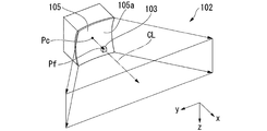
- the light emitting element 102 includes a package 104, a concave mirror 105, a light source 103, a reflection mirror 106, and a light transmission member 107.
- Reference symbol Pf denotes a focal point in a cross section parallel to the xz plane of the concave mirror 105.
- Reference numeral Pc is a position (vertex) farthest from the light source 103 of the concave mirror 105.
- Reference sign CL is the central axis of the concave mirror 105 (a line connecting the vertex Pc of the concave mirror 105 and the focal point Pf of the concave mirror 105).
- the central axis CL of the concave mirror 105 coincides with the optical axis of the light reflected by the concave mirror 105. Therefore, in the example of FIG. 2, the central axis CL coincides with the normal line (x axis) of the light emission surface 107 a of the light emitting element 102.
- the concave mirror 105 is provided in the concave portion 104 a of the package 104.
- the shape of the concave mirror 105 is a curved surface shape following the shape of the concave portion 104 a of the package 104.
- the concave mirror 105 is a parabolic mirror that reflects the light emitted from the light source 103.
- the shape of the concave portion 104a is formed by pressing a mold having a convex shape obtained by inverting the shape of the concave portion 104a to the surface of the resin member to be the package 104, for example.
- the shape of the recess 104a may be formed by cutting the surface of a flat resin member.
- the light source 103 is, for example, a substantially rectangular parallelepiped chip LED (surface mounting LED).
- the light source 103 is disposed at the focal point of the concave mirror 105.
- the central axis CL of the concave mirror 105 coincides with the normal line of the light emission surface of the light source 103 (the normal line of the upper surface of the chip LED).
- the light-transmitting member 107 that transmits the light emitted from the light source 103 is filled in the recess 104 a of the package 104.
- the light source 103 is embedded in the light transmitting member 107.
- the light transmitting member 107 is formed, for example, by forming the concave mirror 105 in the concave portion 104 a of the package 104, disposing the light source 103 and the reflecting mirror 106 inside the package 104, and then transmitting light such as acrylic resin inside the package 104. It is formed by injecting and curing a resin having the following.
- the refractive index of the light transmitting member 107 is set to the same value as the refractive index of the light guide 101.
- the surface 107 a exposed to the outside of the light transmitting member 107 is a light emitting surface of the light emitting element 102.
- the concave portion 104a of the package 104 is filled with the light transmitting member 107 that transmits the light emitted from the light source 103, but the present embodiment is not limited to this.
- a gas such as air may be present in the recess 104 a of the package 104.
- the light source 103 is fixed to the package 104 by a fixing member.
- the reflection mirror 106 is formed by forming a metal film such as aluminum on the mounting substrate of the light source 103 by sputtering or vapor deposition.
- the reflection mirror 106 reflects the light from the light source 103 emitted in a different direction from the concave mirror 105 toward the concave mirror 105.
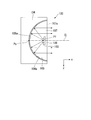
- FIG. 3A is an enlarged view of the light emitting element 102.
- FIG. 3B is a diagram illustrating a cross section of the concave mirror 105 parallel to the xz plane and the angular distribution of the light reflected by the concave mirror 105 in the xz plane.
- FIG. 3C is a diagram illustrating a cross section of the concave mirror 105 parallel to the xy plane and an angle distribution in the xy plane of the light reflected by the concave mirror 105.
- the concave mirror 105 is a parabolic mirror having a vertex Pc at a position farthest from the light source 103.
- the reflecting surface 105a of the concave mirror 105 is an anamorphic reflecting surface having different cross-sectional curvatures at the vertex Pc when the reflecting surface 105a is cut by two orthogonal planes including the central axis CL of the concave mirror 105. It is.
- the horizontal axis is the reflected light exit angle (the exit angle when it is emitted in the direction parallel to the central axis CL is 0 °), the vertical axis is the amount of light emitted at this exit angle, and the light amount is A plane perpendicular to the optical axis (the central axis CL of the concave mirror 105) of the reflected light, with the absolute value
- the direction in which the light diffusion angle is large is the direction (y direction) perpendicular to the normal line of the light exit surface 101b of the light guide 101 and perpendicular to the light propagation direction. This is a direction (z direction) parallel to the normal line of the light exit surface 101b of the light body 101.
- the shape of the cross section parallel to the xz plane and the cross section parallel to the xy plane of the reflecting surface 105a is a parabola.
- the curvature of the parabola in the cross section 105B parallel to the xz plane of the reflective surface 105a is larger than the curvature of the parabola in the cross section 105A parallel to the xy plane of the reflective surface 105a. Therefore, the angular distribution of the light reflected by the reflecting surface 105a has a small spread in the z direction and a large spread in the y direction.
- the diffusion angle D1 in the z direction is
- the diffusion angle D2 in the z direction is
- the focal point Pf is the focal point of the parabola in the cross section parallel to the xz plane of the reflecting surface 105a.
- the curvature of the parabola in the cross section 105B parallel to the xz plane of the reflective surface 105a is different from the curvature of the parabola in the cross section 105A parallel to the xy plane of the reflective surface 105a. Therefore, the focal point Pf is different from the parabolic focal point in the cross section 105A parallel to the xy plane of the reflecting surface 105a.
- the light source 103 is disposed at a parabolic focal point Pf in a cross section 105B parallel to the xz plane of the reflecting surface 105a. Therefore, the light reflected by the reflecting surface 105a is substantially parallel light in a plane parallel to the xz plane, and the diffusion angle D1 is approximately 0 °.
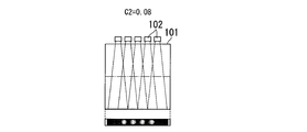
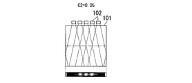
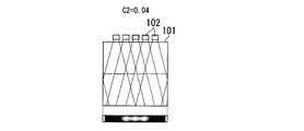
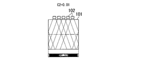
- the curvature C1 of the parabola in the cross section parallel to the xz plane of the reflecting surface 105a is fixed to 0.1
- the curvature C2 of the parabola in the cross section parallel to the xy plane of the reflecting surface 105a is 0.01 to.
- the upper side is a plan view of the light guide 101 and the light emitting element 102 as viewed from the z direction
- the lower side is the inside of the light guide in the AA ′ cross section of the light guide 101. It is a figure which shows light quantity distribution.
- the spread of the light emitted from the light emitting element 102 in the y direction varies depending on the parabolic curvature C2 of the reflecting surface 105a in a cross section parallel to the xy plane. Increasing the curvature C2 reduces the spread of light in the y direction, and decreasing the curvature C2 increases the spread of light in the y direction.
- the curvature C2 is 0.09, the light emitted from the light emitting element 102 is substantially parallel light when viewed from the z direction.
- a large light quantity peak occurs at a position facing each light emitting element 102. Since the light does not spread sufficiently at the boundary between adjacent light emitting elements 102, the boundary becomes dark.
- the diffusion angle D1 in the z direction of the light emitted from the light emitting element 102 is smaller than the diffusion angle D2 in the y direction. Therefore, the spread of light in the z direction can be suppressed while allowing the spread of light in the y direction.
- the light When viewed in the xz plane, the light has a high directivity, so that the optical axis of the light emitting element 102 (the central axis CL of the concave mirror 105) is a critical angle with respect to the light exit surface 101b of the light guide 101. If the angle is set to the above angle, the amount of light leaking outside from the light exit surface 101b of the light guide 101 is very small.
- the light When viewed on the xy plane, the light has a large spread in the y direction and has a small directivity. Therefore, the light emitted from the light emitting element 102 spreads to the boundary between adjacent light emitting elements 102, and the boundary The amount of light increases. As a result, the light amount distribution is made uniform throughout the light guide, and the light control device has less luminance unevenness.
- FIG. 5A is a perspective view of the light control device 111 of the second embodiment.
- FIG. 5B is an enlarged view of the light emitting element 110 provided in the light control device 111.
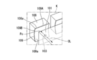
- the light control device 111 is different from the light control device 100 of the first embodiment in that the curvature of the cross section parallel to the xy plane of the reflection surface 109a of the light emitting element 110 is set to zero.
- Constituent elements common to the light control device 100 of the first embodiment in the light control device 111 are denoted by the same reference numerals, and detailed description thereof is omitted.
- the light control device 111 includes a light guide body 101 and a plurality of light emitting elements 110 that allow light to enter the light incident surface 101 a of the light guide body 101.
- the light emitting element 110 includes a package 108, a concave mirror 109, and a light source 103.
- the concave mirror 109 is provided in the concave portion 108 a of the package 108.
- the shape of the concave mirror 109 is a curved surface shape following the shape of the concave portion 108 a of the package 108.
- the concave mirror 109 is a parabolic mirror having a vertex Pc at the position farthest from the light source 103.
- the reflection surface 109a of the concave mirror 109 has a vertex Pc when the reflection surface 109a is cut by two planes orthogonal to each other including the central axis CL of the concave mirror 109 (the optical axis of the light reflected by the reflection surface 109a). It is an anamorphic reflective surface from which the curvature of a cross section differs in each other. Assuming that two directions orthogonal to each other in a plane perpendicular to the optical axis CL of the light reflected by the reflecting surface 109a are a first direction and a second direction, the light in the first direction and the second direction Are different from each other.
- the direction in which the light diffusion angle is large is the direction (y direction) perpendicular to the normal line of the light exit surface 101b of the light guide 101 and perpendicular to the light propagation direction. This is a direction (z direction) parallel to the normal line of the light exit surface 101b of the light body 101.
- the shape of the cross section 109B parallel to the xz plane of the reflective surface 109a is a parabola
- the shape of the cross section 109A parallel to the xy plane of the reflective surface 109a is a straight line.
- the curvature of the cross section 109A is 0, and the curvature of the cross section 109B is greater than zero.
- the light source 103 is arranged at the focal point of the parabola in the cross section 109B of the reflecting surface 109a. Therefore, the angular distribution of the light reflected by the reflecting surface 109a has a small spread in the z direction and a large spread in the y direction. Since the spread of light in the z direction is smaller than the spread of light in the y direction, the diffusion angle in the z direction is smaller than the diffusion angle in the y direction.
- FIG. 6 is a diagram showing a light amount distribution inside the light guide.
- the upper side is a plan view of the light guide 101 and the light emitting element 110 viewed from the z direction, and the lower side shows the light amount distribution inside the light guide in the AA ′ cross section of the light guide 101.
- FIG. 6 is a diagram showing a light amount distribution inside the light guide.
- the upper side is a plan view of the light guide 101 and the light emitting element 110 viewed from the z direction
- the lower side shows the light amount distribution inside the light guide in the AA ′ cross section of the light guide 101.
- the curvature of the cross section 109A of the reflecting surface 109a is zero. Therefore, the reflecting surface 109a has no light collecting action with respect to the spread of light in the y direction. Therefore, the light emitted from the light emitting element 110 spreads to the boundary portion between the adjacent light emitting elements 102, and the amount of light at the boundary portion increases. Therefore, the light quantity distribution in the AA ′ cross section of the light guide 101 is made uniform. Therefore, the light control device 111 with little luminance unevenness is obtained.
- FIG. 7 is an enlarged view of the light emitting element 114 provided in the light control device of the third embodiment.
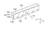
- the light emitting element 114 is different from the light emitting element 102 of the first embodiment in that a plurality of light sources 103 are integrally attached to a long-axis package 112 having a length corresponding to a plurality of light emitting elements.
- Constituent elements common to the light emitting element 102 of the first embodiment in the light emitting element 114 are denoted by the same reference numerals, and detailed description thereof is omitted.
- the package 112 is formed with a plurality of recesses 112a corresponding to the light sources 103 along the y direction.
- Concave mirrors 113 are formed in the plurality of recesses 112a.
- the shape of the concave mirror 113 is a curved surface shape following the shape of the concave portion 112a of the package 112.
- the concave mirror 113 is a parabolic mirror that reflects the light emitted from the light source 103.
- the shape of the recess 112a is formed, for example, by pressing a mold having a convex shape obtained by inverting the shape of the recess 112a on the surface of the resin member to be the package 112.
- the shape of the recess 112a may be formed by cutting the surface of a flat resin member.
- the concave mirror 113 is a parabolic mirror whose apex Pc is the position farthest from the light source 103.
- the reflecting surface 113a of the concave mirror 113 has a vertex Pc when the reflecting surface 113a is cut by two planes orthogonal to each other including the central axis CL of the concave mirror 113 (the optical axis of light reflected by the reflecting surface 113a). It is an anamorphic reflective surface from which the curvature of a cross section differs in each other.
- the shapes of the cross section 113B parallel to the xz plane and the cross section 113A parallel to the xy plane of the reflecting surface 113a are both parabolas.
- the curvature of the parabola in the cross section 113B parallel to the xz plane of the reflection surface 113a is larger than the curvature of the parabola in the cross section 113A parallel to the xy plane of the reflection surface 113a.
- the light source 103 is disposed at the focal point of the parabola in the cross section 113B parallel to the xz plane of the reflection surface 113a.
- the angular distribution of the light reflected by the reflecting surface 113a has a small spread in the z direction and a large spread in the y direction. Since the spread of light in the z direction is smaller than the spread of light in the y direction, the diffusion angle in the z direction is smaller than the diffusion angle in the y direction.
- a plurality of light sources 103 are packaged in the same package. Therefore, the number of parts is reduced, and the light emitting element 114 can be easily attached to the light guide.
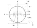
- [Fourth Embodiment] 8A to 10 show a light emitting device 302 according to the fourth embodiment.
- the difference between the issuing element 302 of the present embodiment and the light emitting element 102 of the first embodiment is the shape of the reflecting surface of the concave mirror and the shape of the light source.
- Constituent elements common to the light emitting element 102 of the first embodiment in the light emitting element 302 are denoted by the same reference numerals, and detailed description thereof is omitted.
- the light emitting element 102 has a cross section at a vertex Pc when the reflecting surface 105a of the concave mirror 105 is cut by two planes orthogonal to each other including the central axis CL of the concave mirror 105.
- the anamorphic reflecting surfaces have different curvatures.
- the reflecting surface 305 a of the concave mirror 305 is cut along a plane such as parallel to the X axis through the vertex PC.
- the cross section is substantially the same.
- the dimension W Y along the Y axis is larger than the dimension W Z along the Z axis direction.
- FIG. 9 is a cross-sectional view of the light-emitting element 302 taken along the line AA ′ in FIG. 8A.
- the dimension W Z along the Z direction of the light emitting element 303 is sufficiently small, and the light emission surface of the light source 303 substantially coincides with the focal point Pf of the paraboloid of the reflecting surface 305a. Therefore, the light reflected by the reflecting surface 305a is substantially parallel light in a plane parallel to the xz plane, and the diffusion angle is approximately 0 °.
- FIG. 10 is a cross-sectional view of the light-emitting element 302 in FIG. 8A taken along the line BB ′.
- a part of the light emission surface of the light source 303 is a parabolic surface of the reflective surface 305a. It deviates from the focal point Pf. Therefore, the light reflected by the reflecting surface 305a is diffused in a plane parallel to the xz plane.
- the spread of the light emitted from the light emitting element 302 in the y direction varies depending on the dimension W Y along the Z direction of the light source 303. Increasing the dimension W Y increases the spread of light in the y direction, and decreasing the dimension W Y decreases the spread of light in the y direction.
- the diffusion angle in the z direction of light emitted from the light emitting element 302 of the present embodiment is smaller than the diffusion angle in the y direction. Therefore, the spread of light in the z direction can be suppressed while allowing the spread of light in the y direction.
- the light When viewed in the xz plane, the light has a high directivity. When viewed on the xy plane, the light has a large spread in the y direction and has a small directivity. Therefore, the light emitted from the light emitting element 302 spreads to the boundary between adjacent light emitting elements 302, and the boundary portion. The amount of light increases.
- the light control device having the light emitting device 302 of the present embodiment is a light control device with less luminance unevenness.
- FIG. 11A is a perspective view of the light control device 400 of the present embodiment.
- FIG. 11B is a cross-sectional view of the light control device 400 of the present embodiment.
- the same reference numerals are given to the same components as those of the light control device 100 of the first embodiment, and detailed description thereof is omitted.
- the light control device 400 of this embodiment includes a light emitting element 102, a light guide 410, and a prism sheet 420. Since the light emitting element 102 has the same configuration as the light emitting element of the first embodiment, a detailed description thereof is omitted. In addition, the light emitting element 102 in this embodiment can be applied also when light with low directivity is emitted when viewed in the xz plane.
- the light guide 410 has a function of causing light emitted from the light emitting element 102 to enter from the end surface 411 and to emit light from the light emitting surface 412 while propagating inside.
- the prism sheet 420 has a function of changing the traveling direction of light emitted from the light exit surface 412 of the light guide 410 to a direction closer to the normal line of the light exit surface 412. As shown in FIGS. 11A and 11A, the light emitting element 102 is disposed on the end surface 411 of the light guide 410. The prism sheet 420 is disposed so as to face the light exit surface 412 of the light guide 410.
- the light guide 410 is a plate made of a resin having optical transparency such as acrylic resin.
- the light guide 410 has a wedge shape whose thickness gradually decreases from the end surface 411 provided with the light emitting element 102 toward the tip. That is, as shown in FIG. 11B, the planar shape of the light guide 410 in the zx plane is a right triangle.
- the end surface 411 of the light guide is a light incident surface on which light emitted from the light emitting element 102 is incident. Light from the light emitting element 102 propagates through the light guide 410 and is emitted from the light exit surface 412.
- the reflection surface 413 facing the light emission surface 412 has a certain inclination angle with respect to the light emission surface 412.
- the inclination angle ⁇ 5 of the reflecting surface 413 with respect to the light emitting surface 412 (the angle formed by the light emitting surface 412 and the reflecting surface 413, sometimes referred to as the tip angle of the light guide 410) is set to about 2 °, for example.
- the reflective surface 413 is provided with a metal film having a high light reflectance such as aluminum.
- the metal film may be a metal film formed on the reflecting surface 413 by vapor deposition or the like, or a metal plate produced separately from the light guide 410 is bonded with an optical adhesive. May be. Each time the light L is reflected by the light emitting surface 412 and the reflecting surface 413, the incident angle to the light emitting surface 412 and the reflecting surface 413 is reduced.
- the critical angle at the light exit surface 412 of the light guide 410 that is, the light guide 410. From the Snell's law, the critical angle at the interface between the acrylic resin that constitutes the air and air is about 42 °.
- the incident angle of the light L on the light exit surface 412 is larger than 42 ° which is a critical angle, the total reflection condition is satisfied. The light L is totally reflected by the light exit surface 412.
- the light L repeatedly reflects between the light exit surface 412 and the reflection surface 413, and the total reflection condition is satisfied when the incident angle of the light L on the light exit surface 412 becomes smaller than 42 ° which is a critical angle.
- the light L is emitted to the external space.
- the light L is confined inside the light guide 410 while the incident angle on the light exit surface 412 is larger than the critical angle, and when the incident angle on the light exit surface 412 becomes smaller than the critical angle.
- the light is emitted sequentially from the light exit surface 412. Since the light L is refracted when it is emitted from the light emission surface 412, light having an incident angle of about 42 ° to the light emission surface 412 is emitted as light having an emission angle of about 70 °.
- the light L3 when viewed in a plane (xz plane) parallel to the light propagation direction and perpendicular to the light exit surface 412 of the light guide 410, the light L3 has directivity when it enters the light guide 410. Although it does not have, it has high directivity at the time of emitting from the light guide 410.
- the emission angle of the light L3 when emitted from the light guide bar 410 is about 70 °, and the light L3 is emitted in a substantially horizontal direction. Therefore, using the prism 430, the light L ⁇ b> 3 emitted from the light guide bar 410 is raised in a direction close to the normal direction of the emission surface 412 of the light guide bar 410.
- a prism 430 having a prism structure 431 with a tip angle ⁇ 2 of about 38.5 ° is used, and light L3 is incident from the first surface 431a of the prism structure 431 and reflected by the second surface 431b.
- the light guide bar 410 can be raised in a substantially normal direction with respect to the light exit surface 412.
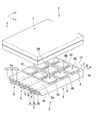
- FIG. 12 is an exploded perspective view of a liquid crystal display device (display device) 1 including the light control device according to the sixth embodiment.
- the light control device functions as the backlight 3.
- the liquid crystal display device 1 has a liquid crystal panel 2 (display element) and a backlight 3 disposed on the back side of the liquid crystal panel 2.
- the liquid crystal panel 2 is a transmissive liquid crystal panel that performs display using light emitted from the backlight 3. The user can view the display from the opposite side of the backlight 3, that is, from the upper side of the liquid crystal panel 2 in FIG.
- the configuration of the liquid crystal panel 2 is not particularly limited, and may be an active matrix liquid crystal panel provided with a switching thin film transistor (Thin Film Transistor, hereinafter abbreviated as TFT) for each pixel, or provided with a TFT. It may be a simple matrix type liquid crystal panel.
- TFT Thin Film Transistor
- the liquid crystal panel is not limited to a transmissive liquid crystal panel, and may be a transflective liquid crystal panel.
- the display mode is not particularly limited, and there are various display modes such as VA (Vertical Alignment) mode, TN (Twisted Nematic) mode, STN (Super Twisted Nematic) mode, IPS (In-Plane Switching) mode, etc.
- VA Very Alignment
- TN Transmission Nematic
- STN Super Twisted Nematic
- IPS Intelligent Nematic Switching
- a liquid crystal panel can be used.
- the backlight 3 is composed of three backlight units 4 having the same dimensions, shape and configuration.
- the three backlight units 4 are in a direction orthogonal to the longitudinal direction of the light guide 5, that is, in a direction (y direction) orthogonal to the direction in which the three light extraction regions RA, RB, RC of the light guide 5 are arranged. It is arranged adjacent to each other. Therefore, the backlight 3 has a total of nine light extraction regions RA, RB, RC, three in each of the horizontal and vertical directions on the screen of the liquid crystal display device 1.
- Each backlight unit 4 includes an illumination unit 6 and a light guide 5.
- the illumination unit 6 is composed of a plurality (three in the example of FIG. 12) of light emitting elements 7a, 7b, and 7c.
- the light emitting elements 7a, 7b, and 7c are light emitting elements having the configuration shown in the first embodiment or the second embodiment. That is, when two directions orthogonal to each other in a plane perpendicular to the optical axis of light emitted from the light emitting surface of the light emitting element are defined as the first direction and the second direction, the first direction and The light emitting elements have different diffusion angles of light in the second direction.
- the direction in which the light diffusion angle is large is a direction (y direction) orthogonal to the normal line of the main surface 5a of the light guide 5 and orthogonal to the light propagation direction, and the direction in which the light diffusion angle is small is the light guide. It is a direction (z direction) parallel to the normal line of the main surface 5a of the body 5.
- the main surface 5 a of the light guide 5 is a light emission surface from which light propagated through the light guide 5 is emitted toward the liquid crystal panel 2.
- the light guide 5 is composed of a parallel plate made of a resin having optical transparency such as acrylic resin.
- the backlight 3 is composed of three backlight units 4 in which the light guide 5 is a separate body.
- the backlight 3 has a total of nine light extraction regions RA, RB, RC.
- the light body may have an integral structure. Even with this structure, it is possible to select the light extraction regions RA, RB, and RC for emitting light by using a light emitting element with high directivity.
- Three light emitting elements 7a, 7b, 7c are installed on one end face of the light guide 5 with the light emission side facing the light guide 5 side.
- the light guide 5 receives light emitted from the light emitting elements 7a, 7b, and 7c, totally reflects the light internally, and is opposite to the end face side where the light emitting elements 7a, 7b, and 7c are installed. It has a function of propagating toward the end face (from the ⁇ x direction to the + x direction in FIG. 12) and taking it out to the external space. Further, the three light emitting elements 7a, 7b, and 7c can be individually controlled to be turned on / off, and the amount of emitted light can be controlled. Thereby, the backlight 3 functions as a light control element which can adjust the light quantity of the light inject
- the backlight 3 includes a printed wiring board on which the light emitting elements 7a, 7b, and 7c are mounted, a control unit that includes a driving IC for driving and controlling the light emitting elements 7a, 7b, and 7c, and the like. It has been.
- the light emitting elements 7a, 7b, and 7c it is preferable to use light emitting elements having high directivity in the xz plane. For example, the intensity distribution with respect to the spread angle of the emitted light while the light is guided through the light guide 5 is used. Those having a half width (diffusion angle in the xz plane) of about 5 ° can be used.
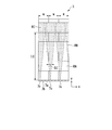
- a plurality of (three in the present embodiment) light extraction regions RA, RB, RC are arranged in the longitudinal direction of the light guide 5 on the main surface 5 a facing the liquid crystal panel 2. (In the x-axis direction in FIG. 12).
- low refractive index bodies 8a and 8b having a refractive index lower than that of the light guide 5 and a refractive index body having a refractive index equal to the refractive index of the light guide 5 are provided in each of the light extraction regions RA, RB, and RC. 9 is provided.
- region RC On the low refractive index bodies 8a and 8b and the refractive index body 9, light scatterers 10 that scatter light emitted from the low refractive index bodies 8a and 8b and the refractive body 9 are stacked.
- the respective light extraction regions are directed from the side closer to the light emitting elements 7a, 7b, 7c to the side farther from the first light extraction region RA, the second light extraction region RB, and the third light extraction. This is referred to as region RC.
- the main surface of the light guide 5 provided with the light extraction regions RA, RB, RC is the first main surface 5a
- the main surface opposite to the first main surface 5a is the second main surface 5b
- the light emitting element 7a is the first end surface 5c
- the end surface of the light guide 5 provided with 7b and 7c is referred to as a first end surface 5c
- the end surface opposite to the first end surface 5c is referred to as a second end surface 5d.
- the low refractive index bodies 8 a and 8 b both have a refractive index lower than the refractive index of the light guide 5, and the refractive index body 9 has a refractive index equal to the refractive index of the light guide 5.
- the low refractive index bodies 8a and 8b and the refractive index body 9 have different refractive indexes. Further, the low refractive index bodies 8a and 8b and the refractive index body 9 are arranged along the propagation direction of light emitted from the light emitting elements 7a, 7b and 7c and incident on the light extraction regions RA, RB and RC (FIG. 12 from the ⁇ x direction to the + x direction) in order of relatively low refractive index to relatively high refractive index.
- the refractive index nWG of the light guide 5 is 1.5
- the refractive index nA of the first low refractive index body 8a provided in the first light extraction region RA is 1.3
- the refractive index nB of the second low refractive index body 8b provided in the region RB is 1.4
- the refractive index nC of the refractive index body 9 provided in the third light extraction region RC is 1.5.
- Examples of methods for forming the low refractive index bodies 8a and 8b and the refractive index body 9 having different refractive indexes include the following two methods.
- the first method is to form the low refractive index bodies 8a and 8b and the refractive index body 9 using different materials.
- an acrylic resin is used as the material of the light guide 5
- Kuraray Co., Ltd. as the material of the refractive index body 9.
- the refractive index body 9 has the same refractive index as that of the light guide body 5, it is not always necessary to form the refractive index body 9 on the light guide body 5.
- the light scatterer 10 may be merely disposed on the light guide 5.
- the second technique is to use a material containing a low refractive index material in a predetermined substrate and adjust the refractive index by varying the concentration of the low refractive index material.
- Low refractive index materials such as powder (registered trademark, refractive index: 1.27) or airgel (registered trademark, refractive index: 1.27) manufactured by Jason Wells are included, and the concentration of these low refractive index materials is different.
- Two types of liquids are prepared. Each liquid material can be selectively applied on the light guide 5 and cured.
- a light scatterer 10 is laminated on the low refractive index bodies 8 a and 8 b and the refractive index body 9.
- the light scatterer 10 has a function of scattering the light incident from the low refractive index bodies 8 a and 8 b and the refractive index body 9 and extracting the light to the external space of the backlight 3.
- the light scatterer 10 a commercially available light scattering film in which scattering beads or the like are coated on the base film can be used, and the light is scattered on the low refractive index bodies 8 a and 8 b and the refractive index body 9.
- the light scatterer 10 can be formed by sticking a scattering film.
- the first end surface 5 c of the light guide 5 is divided into three in the short direction of the light guide 5 (y direction in FIG. 12), and the angles with respect to the first main surface 5 a are different from each other 3.
- Two inclined surfaces 11a, 11b, and 11c are formed.
- a light guide whose angle between the first main surface 5a and the end surface is a right angle is prepared, and the end surface is divided into three regions divided into three regions. It can be formed by a method such as grinding at an angle so as to form a different angle with respect to one principal surface 5a.
- one light emitting element 7a, 7b, 7c is being fixed to the approximate center of each inclined surface 11a, 11b, 11c via the optical adhesive agent one by one. Therefore, three light emitting elements 7 a, 7 b, 7 c are arranged in the short direction of the light guide 5 over the entire first end face 5 c.
- the inclined surface (right side in FIG. 12) having the smallest angle with respect to the first main surface 5a is defined as the first light incident surface.
- the inclined surface (center of FIG. 12) having the next smallest angle with respect to the first main surface 5a is the second light incident surface 11b
- the inclined surface (left side of FIG. 12) having the largest angle with respect to the first main surface 5a is third. This is referred to as a light incident surface 11c.
- the light emitting element provided on the first light incident surface 11a is provided on the first light emitting element 7a
- the light emitting element provided on the second light incident surface 11b is provided on the second light emitting element 7b and the third light incident surface 11c.
- the light emitting element is referred to as a third light emitting element 7c.
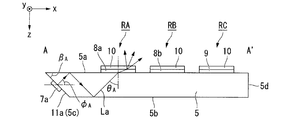
- FIG. 13A is a cross-sectional view taken along the line A-A ′ of FIG.
- FIG. 13B is a sectional view taken along line B-B ′ of FIG.
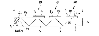
- FIG. 13C is a cross-sectional view taken along line C-C ′ of FIG.
- the angle ⁇ A formed by the first light incident surface 11a and the first main surface 5a is set to 55 °.
- Angle beta B of the second light incident surface 11b and the first major surface 5a is set to 65 °.
- the angle ⁇ C formed by the third light incident surface 11c and the first main surface 5a is set to 75 °.
- Each light emitting element 7a, 7b, 7c is fixed so that light La, Lb, Lc is incident perpendicularly to each light incident surface 11a, 11b, 11c.
- the light La, Lb, Lc emitted from each light emitting element 7a, 7b, 7c repeats total reflection between the first main surface 5a and the second main surface 5b of the light guide 5, and is on the first end surface 5c side. To the second end face 5d side.
- the propagation angle ⁇ A of the light La from the first light emitting element 7a is 35 °
- 2 propagation angle phi B light Lb from the light emitting element 7b is 25 °
- the propagation angle phi C of the light Lc from the third light-emitting element 7c is 15 °. Therefore, while each light La, Lb, Lc is propagated from the first end face 5c side toward the second end face 5d side, the first light extraction area RA, the second light extraction area RB, and the third light extraction area RC. In this order, the light enters the light extraction areas RA, RB, RC.
- the thickness (dimension in the z direction) is drawn sufficiently larger than the longitudinal dimension (dimension in the x direction) of the light guide 5 in order to make the drawings easy to see. Since only the central axis of the light emitted from 7a, 7b, and 7c is drawn, it seems that the light may not necessarily enter each of the light extraction regions RA, RB, and RC.
- the light La, Lb, Lc from the light emitting elements 7a, 7b, 7c has a finite light beam diameter, so that the light La, Lb, Lc The light is reliably incident on the light extraction areas RA, RB, RC.
- the illuminating unit 6 of the present embodiment includes three light emitting elements 7a, 7b, and 7c.
- Lights La, Lb, and Lc from the light emitting elements 7a, 7b, and 7c are converted into the light extraction regions RA
- Lights La, Lb, and Lc are extracted from RB and RC and are incident on the light extraction regions RA, RB, and RC at an incident angle including an incident angle at which the light can be extracted.
- the light La, Lb, and Lc from each light emitting element 7a, 7b, and 7c are the light guide 5 in each light extraction area
- the incident angle range in which light can be extracted outside in the first light extraction area RA is 60. Less than 1 °, the incident angle range in which light can be extracted outside in the second light extraction region RB is less than 69.0 °, and the incident angle range in which light can be extracted outside in the third light extraction region RC is all angles. It becomes a range.
- the two low refractive index bodies 8a and 8b and the refractive index body 9 provided in the three light extraction regions RA, RB, and RC of the present embodiment are incident on the light extraction regions RA, RB, and RC.
- the light is arranged in the order of relatively low refractive index to relatively high refractive index.
- the three light extraction regions RA, RB, and RC have different incident angle ranges in which light can be extracted to the outside.
- the three light extraction areas RA, RB, and RC have a relatively narrow incident angle range that can be extracted from a light extraction area that has a relatively narrow incident angle range along the propagation direction of incident light.
- incident angle range that can be extracted in the first light extraction region RA is less than 60.1 °
- incident angle range that can be extracted in the second light extraction region RB is less than 69.0 °
- third light The range of incident angles that can be extracted in the extraction region RC is arranged in the order of all angle ranges).
- the second light incident surface 11b and the first main light emitting element 7b are turned on.
- the angle ⁇ B formed with the surface 5a is 65 °, and the light Lb from the second light emitting element 7b is perpendicularly incident on the second light incident surface 11b, so that the light Lb from the second light emitting element 7b
- the incident angle ⁇ B with respect to one principal surface 5a is 65 °.
- the critical angle ⁇ B here is 69.0 °
- the light Lb passes through the interface between the light guide 5 and the second low refractive index body 8b and is incident on the second low refractive index body 8b. Thereafter, the light scatterer 10 is taken out to the outside. In this way, substantially the entire amount of the light Lb emitted from the second light emitting element 7b can be extracted from the second light extraction region RB.
- the backlight 3 of the present embodiment can extract light emitted from a predetermined light emitting element only from a predetermined light extraction region.
- the third light incident surface 11c and the first main light emitting element 7c are turned on. Since the angle ⁇ C formed with the surface 5a is 75 ° and the light Lc from the third light emitting element 7c is perpendicularly incident on the second light incident surface 11c, the light Lc from the third light emitting element 7c The incident angle ⁇ C with respect to one principal surface 5a is 75 °.
- 14A to 14C are diagrams showing light diffusion angles DA, DB, and DC in the y direction of the first light emitting element 7a, the second light emitting element 7b, and the third light emitting element 7c.
- the light diffusion angles DA, DB, and DC (spread of light in the y direction) of the first light emitting element 7a, the second light emitting element 7b, and the third light emitting element 7c are different from each other.
- the light diffusion element in which light is extracted from the light extraction region close to the first end face 5c has a larger light diffusion angle in the y direction.
- the light diffusion angle DA in the y direction of the first light emitting element 7a from which light is extracted from the first light extraction region RA closest to the first end face 5c is the largest.
- the second light emitting element 7b from which light is extracted from the second light extraction region RB next to the first end surface 5c next to the first light extraction region RA has the second largest light diffusion angle DB in the y direction.
- the light diffusion angle DC in the y direction of the third light emitting element 7c from which light is extracted from the third light extraction region RC farthest from the first end face 5c is the smallest.
- the distance from the first end face 5c to the first light extraction area RA is LA
- the distance from the first end face 5c to the second light extraction area RB is LB
- the distance from the first end face 5c to the third light extraction area RC is LC.
- the width of the light guide 5 in the y direction is W
- the diffusion angle of light in the y direction of the first light emitting element 7a is DA
- the diffusion angle of light in the y direction of the second light emitting element 7b is DB
- the third light emitting element 7c If the diffusion angle of light in the y direction is DC, the diffusion angles DA, DB, DC satisfy the following equations.
- the light emitted from the first light emitting element 7a propagates in the x direction inside the light guide 5 while spreading in the y direction.
- the light emitted from the first light emitting element 7a reaches the first light extraction region RA, it spreads to a position separated by W / 2 or more in the + y direction and the ⁇ y direction. Therefore, the lights emitted from the adjacent first light emitting elements 7a overlap with each other, and a uniform amount of light can be obtained in the entire first light extraction region RA.
- the light emitted from the second light emitting element 7b propagates in the x direction in the light guide 5 while spreading in the y direction.
- the light emitted from the second light emitting element 7b spreads to a position separated by W / 2 or more in the y direction when it reaches the second light extraction region RB. Therefore, the lights emitted from the adjacent second light emitting elements 7b overlap with each other, and a uniform amount of light can be obtained in the entire second light extraction region RB.
- the light emitted from the third light emitting element 7c propagates in the x direction inside the light guide 5 while spreading in the y direction.
- the light emitted from the third light emitting element 7c reaches the third light extraction region RC, the light spreads to a position separated by W / 2 or more in the + y direction and the ⁇ y direction. Therefore, the lights emitted from the adjacent third light emitting elements 7c overlap each other, and a uniform amount of light can be obtained in the entire third light extraction region RC.
- the three light extraction regions RA, RB, RC depend on which one of the three light emitting elements 7a, 7b, 7c of each backlight unit 4 is turned on. It is possible to select as appropriate from which light extraction region of the light extraction region, that is, which light extraction region RA, RB, RC emits light. Further, by controlling the amount of light emitted from each light emitting element 7a, 7b, 7c, the amount of light extracted from the selected light extraction regions RA, RB, RC, that is, the brightness of the selected light extraction region. Can be adjusted.
- the backlight 3 of the present embodiment can control whether or not light is emitted from each of the light extraction regions RA, RB, and RC simply by switching the light emitting elements 7a, 7b, and 7c to be lit. Therefore, by efficiently taking out the light emitted from the illumination unit 6 from the light guide 5, a sufficient amount of light can be obtained and a backlight with high contrast can be realized. Furthermore, the structure can be simplified, the thickness can be reduced, and the inexpensive backlight 3 can be realized. In addition, by using the backlight 3 described above, it is possible to realize the liquid crystal display device 1 that can display brightly and with high contrast.
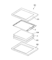
- FIG. 15 is an exploded perspective view showing a schematic configuration of a liquid crystal display device which is one configuration example of the display device.
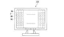
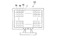
- FIG. 16A, FIG. 16B, FIG. 17A, and FIG. 17B are diagrams showing examples of backlight arrangement in the liquid crystal display device.
- the liquid crystal display device 121 of this configuration example includes a lower case 122, a reflection plate 123, a backlight 3 (light control device), a diffusion plate 124, and a liquid crystal panel 2 (display element). And an upper case 125. That is, a laminated body of the reflecting plate 123, the backlight 3, the diffusion plate 124, and the liquid crystal panel 2 is accommodated in the lower case 122 and the upper case 125.
- the reflector 123 on the opposite side of the backlight 3 from the liquid crystal panel 2
- light leaking from the backlight 3 to the opposite side of the liquid crystal panel 2 can be reflected and contributed to display.
- the diffusion plate 124 between the backlight 3 and the liquid crystal panel 2
- luminance unevenness of the backlight 3 can be reduced.
- the reflecting plate 123 and the diffusing plate 124 are not necessarily used.
- FIG. 16A a configuration in which a plurality of backlights 3 are arranged in the screen of the liquid crystal display device 121 so that the light extraction areas RA, RB, RC are arranged in the vertical direction of the screen can be employed.
- FIG. 16B a configuration in which a plurality of backlights 3 are arranged in the screen of the liquid crystal display device 127 so that the light extraction areas RA, RB, RC are arranged in the horizontal direction of the screen is adopted. Can do.
- light extraction areas RA, RB, RC are provided only in a part of the longitudinal direction, and the other parts are elongated rod-shaped light guides that are areas where light is guided.
- a backlight 137 combining a plurality of 135 (three in this example) 135 may be used.
- regions where the light extraction regions RA, RB, RC are provided are shifted in the longitudinal direction. Therefore, when a plurality of light guides 135 are combined, the light extraction regions RA, RB, and RC are arranged along the longitudinal direction of the light guide 135.
- a plurality of backlights 137 may be arranged in the screen of the liquid crystal display device 131 so that the light extraction areas RA, RB, RC are arranged in the vertical direction of the screen.
- a plurality of backlights 137 may be arranged in the screen of the liquid crystal display device 133 so that the light extraction areas RA, RB, RC are arranged in the horizontal direction of the screen.
- FIG. 18 is a cross-sectional view of the lighting device as the first configuration example.
- FIG. 19A and FIG. 19B are diagrams illustrating a lighting device that is a second configuration example
- FIG. 19A is a plan view illustrating the lighting device that is a second configuration example.
- FIG. 19B is a cross-sectional view taken along line AA ′ of FIG. 19A.
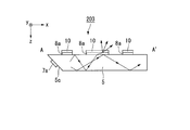
- the first low refractive index body 8a having a refractive index of 1.3 is formed on the first main surface 5a side of the light guide 5 and the refractive index is on the second main surface 5a side.
- a second low refractive index body 8b of 1.4 is formed.
- the light scatterers 10 are stacked on the first low refractive index body 8a and the second low refractive index body 8b, respectively.
- Other configurations are the same as those of the first embodiment.
- FIG. 18 only one first end face 5c is shown, but actually another one first end face having a different angle with respect to the first main face 5a is formed in the depth direction of the paper.
- the light emitting element only one light emitting element 7a is shown, but actually, another one light emitting element is installed in the depth direction of the drawing.
- the light emitting element 201 emits light from the first main surface 5a side depending on which one of the two light emitting elements provided on the first end surface 5c of the light guide 5 is lit. It is possible to switch whether light is emitted from the two principal surfaces 5b side. Therefore, it is possible to realize an illumination device that can switch the light emitting surface.
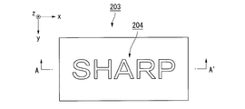
- a character portion 204 written “SHARP” is formed on one surface of the light guide 5.
- a first low refractive index body 8a having a refractive index of 1.3 is formed on the first main surface 5a side of the light guide 5, and the character portion 204 is formed.
- the first low refractive index body 8a is not formed in any other part.
- a light scatterer 10 is stacked on the first low refractive index body 8a. That is, the character part 204 is a light extraction area in the above embodiment. Other configurations are the same as those of the first embodiment.
- FIG. 15B a first low refractive index body 8a having a refractive index of 1.3
- the lighting device 203 light is emitted from the character part 204 depending on which of the two light emitting elements provided on the first end surface 5 c of the light guide 5 is lit, or other than the character part 204. It is possible to switch whether light is emitted from Therefore, according to this structure, the illuminating device which can be utilized as digital signage which can blink the character part 204, for example is realizable.
- FIG. 20 shows a table lamp 400 provided with the light emitting element of the above embodiment as the light source unit 410.
- the light source unit 410 may have a plurality of light emitting elements.
- this desk lamp 400 since the light from the light source unit 410 has high directivity, it is possible to illuminate a narrow range as shown by a solid arrow in FIG.
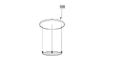
- FIG. 21 shows a ceiling light 500 including the light emitting element or the light source device of the above embodiment.
- the ceiling light 500 may have a plurality of light emitting elements.
- this ceiling light 500 since the light from the surface light source device has high directivity, a narrow range can be illuminated as shown in FIG.
- the aspect of the present invention can be used for a light emitting element, a light control element, a display device, and a lighting device.
- SYMBOLS 1 Liquid crystal display device (display apparatus), 2 ... Liquid crystal panel (display element), 3 ... Backlight, 5 ... Light guide, 7a, 7b, 7c ... Light emitting element, 8a, 8b ... Low refractive index body, 9 ... Refractive index body, 11a, 11b, 11c ... light incident surface, 100 ... back light (dimming element), 101 ... light guide, 101a ... light incident surface, 101b ... light emitting surface, 102 ... light emitting element, 103 ... light source 104 ... package, 104a ... concave, 105 ... concave mirror, 105a ... reflective surface, 105A, 105B ...
- concave mirror 107 ... light transmitting member, 108 ... package, 108a ... concave, 109 ... concave mirror, 109a ... reflective , 109A, 109B ... cross section of concave mirror, 110 ... light emitting element, 111 ... backlight (dimming element), 112 ... package, 112a ... concave, 113 ... concave mirror, 11 a ... reflecting surface, 113A, 113B ... cross section of concave mirror, 121,127,131,133 ... liquid crystal display device (display device), 135 ... light guide, 137 ... backlight (dimming element), 201,203 ...
- Illumination device central axis of concave mirror (optical axis of light reflected by reflecting surface), D1, D2, DA, DB, DC: diffusion angle, Pf: parabolic focus, RA, RB, RC: light extraction region
Landscapes
- Physics & Mathematics (AREA)
- General Physics & Mathematics (AREA)
- Optics & Photonics (AREA)
- Engineering & Computer Science (AREA)
- General Engineering & Computer Science (AREA)
- Planar Illumination Modules (AREA)
- Liquid Crystal (AREA)
- Led Device Packages (AREA)
Abstract
発光素子は、光源と、前記光源から射出された光を反射するミラーと、を備え、ミラーで反射された光の光軸に対して垂直な平面内における互いに直交する2つの方向を第1の方向及び第2の方向としたときに、第1の方向の光の拡散角と第2の方向の光の拡散角は互いに異なる。
Description
本発明は、発光素子、調光素子、表示装置および照明装置に関する。
本願は、2011年5月31日に、日本に出願された特願2011-121671号に基づき優先権を主張し、その内容をここに援用する。
本願は、2011年5月31日に、日本に出願された特願2011-121671号に基づき優先権を主張し、その内容をここに援用する。
導光体の端面に発光素子を配置したサイドライト方式の照明装置として、特許文献1の照明装置が知られている。サイドライト方式の照明装置では、照明光の輝度を高めるために、複数の発光素子を導光体の端面に設置するのが一般的である。この場合、発光素子から射出される光の指向性が高いと、隣接する発光素子の境界部で光の明暗が発生し、輝度むらが発生する惧れがある。そのため、特許文献1の照明装置では、発光素子から射出された光を拡散部材で拡散させて、導光体全体で均一な光量の光が得られるようにしている。
特許文献1の照明装置では、発光素子と導光体との間に拡散部材を設置している。そのため、部品点数が増加し、コストアップの原因となる。また、発光素子から射出された光は、導光体の内部を全反射しながら伝播するため、発光素子から射出された光が導光体の光射出面と直交する方向(導光体の板厚方向)に拡散されると、光が全反射しなくなる。
そのため、導光体の光入射面近傍で光漏れが発生し、輝度むらが発生する。
そのため、導光体の光入射面近傍で光漏れが発生し、輝度むらが発生する。
本発明の態様における目的は、輝度むらを抑制可能な発光素子、調光素子、表示装置および照明装置を提供することにある。
本発明の一態様における発光素子は、光源と、前記光源から射出された光を反射するミラーと、を備え、前記ミラーで反射された光の光軸に対して垂直な平面内における互いに直交する2つの方向を第1の方向及び第2の方向としたときに、前記第1の方向の光の拡散角と前記第2の方向の光の拡散角は互いに異なる。
前記ミラーは、前記ミラーを、前記光軸を含む互いに直交する第1の平面及び第2の平面で切ったときに、その光軸上の点における前記ミラーを前記第1の平面で切ったときの断面の曲率と、前記第2の平面で切ったときの断面の曲率が互いに異なるアナモルフィック形状であってもよい。
前記2つの断面のうち曲率の大きい断面における前記ミラーの形状は放物線であり、前記放物線の焦点に前記光源が配置されていてもよい。
前記2つの断面のうち曲率の小さい断面における前記ミラーの曲率は0であってもよい。
凹部が形成されたパッケージを備え、前記パッケージの前記凹部に前記ミラーが形成され、前記凹部に前記光源から射出された光を透過する光透過部材が充填され、前記光透過部材に前記光源が埋設されていてもよい。
前記光源が一方向に配列して複数設けられ、前記パッケージには、前記複数の光源のそれぞれに対応した前記反射面が複数形成され、前記複数の反射面が前記複数の光源の配列方向に沿って設けられていてもよい。
本発明の他の態様における調光素子は、光入射面と光射出面とを有する導光体と、前記導光体の光入射面に光を入射させる複数の発光素子と、前記導光体上に設けられ、前記導光体の内部を伝播した光を前記導光体の外部に取り出し可能であり、前記光の伝播方向に沿って設けられた複数の光取出領域と、を備え、前記複数の光取出領域から取り出し可能な光の伝播角度は互いに異なり、前記複数の発光素子から射出された光は、互いに異なる伝播角度で前記導光体の内部を伝播し、前記複数の発光素子は、本発明の発光素子であり、前記発光素子において、光の拡散角が大きい方向は、前記導光体の光射出面の法線と直交し且つ前記光の伝播方向と直交する方向であり、光の拡散角が小さい方向は、前記導光体の光射出面の法線と平行な方向である。
前記複数の光取出領域において前記導光体の光射出面と接する部材の屈折率は互いに異なっていてもよい。
前記導光体の光射出面と接する部材の屈折率は、前記導光体の光入射面から遠い位置に配置されたものほど大きくてもよい。
前記導光体の光入射面には、前記導光体の光射出面との成す角度が互いに異なる複数の傾斜面が設けられ、前記複数の発光素子の各々が前記複数の傾斜面の各々に固定されていてもよい。
前記複数の発光素子の一つは、前記光入射面に対して相対的に近い位置の前記光取出領域から取り出される光を射出し、前記複数の発光素子の他の一つは、前記光入射面に対して相対的に遠い位置の前記光取出領域から取り出される光を射出し、前記複数の発光素子の一つが射出する光の前記光射出面の法線と直交し且つ前記光の伝播方向と直交する方向の光の拡散角は、前記複数の発光素子の他の一つが射出する光の前記光射出面の法線と直交し且つ前記光の伝播方向と直交する方向の光の拡散角よりも大きくてもよい。
本発明のさらに他の態様における表示装置は、本発明の調光素子と、前記調光素子から射出される光を用いて表示を行う表示素子と、を備えている。
本発明のさらに他の態様における照明装置は、本発明の調光素子を備えている。
本発明の態様によれば、輝度むらを抑制可能な発光素子、調光素子、表示装置および照明装置を提供することができる。
[第1実施形態]
図1は、第1実施形態の調光装置100の斜視図である。調光装置100としては、例えばバックライトが挙げられる。
図1は、第1実施形態の調光装置100の斜視図である。調光装置100としては、例えばバックライトが挙げられる。
調光装置100は、導光体101と、導光体101の光入射面101aに光を入射させる複数の発光素子102と、を備えている。
導光体101は、平面視矩形の透明な板状部材である。導光体101の端面は光入射面101aであり、導光体101の主面は光射出面101bである。図1では、光射出面101bは、導光体101の2つの主面の双方に設けられているが、光射出面101bは、導光体101の一方の主面のみに設けられていてもよい。図1では、光射出面101bはxy平面と平行な面であり、光入射面101aはyz平面と平行な面である。複数の発光素子102は、導光体101の光入射面101aに沿ってy方向に配列されている。複数の発光素子102は、その光射出面を導光体101の光入射面101aに向けて導光体101の光入射面101aに固定されている。図1では、複数の発光素子102は、導光体101の1つの端面にのみ設けられているが、この端面とX方向において対向する端面に複数の発光素子102を配置し、2つの端面から光を入射する構成としてもよい。
発光素子102から導光体101の光入射面101aに入射した光は、導光体101の内部を全反射しながら概ねx方向に伝播する。そして、導光体101の2つの主面に設けられた図示略の光路変換部材によって、その光路を変換され、導光体101の光射出面101bから射出される。導光体101の光射出面101bから射出される光の光量は、発光素子102から射出される光の光量を変化させることによって制御される。発光素子102は、個々に独立して点灯、消灯が制御でき、さらに射出光量が制御できる構成となっている。これにより、調光装置100は、射出される光の光量を調節可能な調光素子として機能する。
図2は、発光素子102の断面図である。
発光素子102は、パッケージ104と、凹面ミラー105と、光源103と、反射ミラー106と、光透過部材107と、を備えている。符号Pfは、凹面ミラー105のxz平面と平行な断面における焦点である。符号Pcは、凹面ミラー105の光源103から最も離間した位置(頂点)である。符号CLは、凹面ミラー105の中心軸(凹面ミラー105の頂点Pcと凹面ミラー105の焦点Pfとを結ぶ線)である。凹面ミラー105の中心軸CLは、凹面ミラー105で反射された光の光軸と一致する。そのため、図2の例では、中心軸CLは、発光素子102の光射出面107aの法線(x軸)と一致している。
凹面ミラー105は、パッケージ104の凹部104aに設けられている。凹面ミラー105の形状は、パッケージ104の凹部104aの形状に倣った曲面形状となっている。凹面ミラー105は、光源103から射出された光を反射する放物面ミラーである。凹部104aの形状は、例えば、パッケージ104となる樹脂部材の表面に凹部104aの形状を反転させた凸形状を有する金型を押し付けることにより形成されている。凹部104aの形状は、平坦な樹脂部材の表面を切削加工することによって形成しても良い。
光源103は、例えば、略直方体状のチップLED(表面実装用LED)である。光源103は、凹面ミラー105の焦点に配置されている。凹面ミラー105の中心軸CLは、光源103の光射出面の法線(チップLEDの上面の法線)と一致している。
パッケージ104の凹部104aには、光源103から射出された光を透過する光透過部材107が充填されている。光源103は、光透過部材107の内部に埋設されている。光透過部材107は、例えば、パッケージ104の凹部104aに凹面ミラー105を形成し、パッケージ104の内部に光源103および反射ミラー106を配置した後、パッケージ104の内部に、アクリル樹脂等の光透過性を有する樹脂を注入して硬化させることにより形成されている。光透過部材107の屈折率は、導光体101の屈折率と同じ値に設定されている。光透過部材107の外部に露出する面107aは、発光素子102の光射出面となっている。
本実施形態において、パッケージ104の凹部104aには、光源103から射出された光を透過する光透過部材107が充填される例を示しているが、本実施形態はこれに限定されない。パッケージ104の凹部104aには、空気等の気体が存在していてもよい。この場合、光源103は、固定部材によりパッケージ104に固定される。
反射ミラー106は、光源103の実装基板に、例えばアルミニウム等の金属膜をスパッタ法もしくは蒸着法で形成することにより形成されている。反射ミラー106は、凹面ミラー105と異なる方向に射出された光源103からの光を凹面ミラー105に向けて反射する。
図3Aは、発光素子102の拡大図である。図3Bは、凹面ミラー105のxz平面と平行な断面と凹面ミラー105で反射された光のxz平面内での角度分布を示す図である。図3Cは、凹面ミラー105のxy平面と平行な断面と凹面ミラー105で反射された光のxy平面内での角度分布を示す図である。
図3Aに示すように、凹面ミラー105は、光源103から最も離間した位置を頂点Pcとする放物面ミラーである。凹面ミラー105の反射面105aは、この反射面105aを凹面ミラー105の中心軸CLを含む互いに直交する2つの平面で切ったときに、その頂点Pcにおける断面の曲率が互いに異なるアナモルフィック反射面である。
横軸を反射光の射出角度(中心軸CLと平行な方向に射出したときの射出角度を0°とする)とし、縦軸をこの射出角度で射出された光の光量とし、光の光量がピーク光量の50%まで減衰するときの射出角度α,βの差の絶対値|α-β|を拡散角とし、反射光の光軸(凹面ミラー105の中心軸CL)に対して垂直な平面内における互いに直交する2つの方向を第1の方向および第2の方向とすると、第1の方向と第2の方向の光の拡散角は互いに異なる。光の拡散角が大きい方向は、導光体101の光射出面101bの法線と直交し且つ光の伝播方向と直交する方向(y方向)であり、光の拡散角が小さい方向は、導光体101の光射出面101bの法線と平行な方向(z方向)である。
本実施形態の場合、図3B及び図3Cに示すように、反射面105aのxz平面と平行な断面およびxy平面と平行な断面の形状は、いずれも放物線である。反射面105aのxz平面と平行な断面105Bにおける放物線の曲率は、反射面105aのxy平面と平行な断面105Aにおける放物線の曲率よりも大きい。そのため、反射面105aで反射された光の角度分布は、z方向への広がりが小さく、y方向への広がりが大きい。xz平面内において、光の光量がピーク光量の50%まで減衰するときの射出角度はθ1,θ2である。よって、z方向の拡散角D1は|θ1-θ2|である。xy平面内において、光の光量がピーク光量の50%まで減衰するときの射出角度はθ3,θ4である。
よって、z方向の拡散角D2は|θ3-θ4|である。z方向への光の広がりはy方向への光の広がりよりも小さいので、z方向の拡散角D1はy方向の拡散角D2よりも小さい。
よって、z方向の拡散角D2は|θ3-θ4|である。z方向への光の広がりはy方向への光の広がりよりも小さいので、z方向の拡散角D1はy方向の拡散角D2よりも小さい。
図3B及び図3Cにおいて、焦点Pfは、反射面105aのxz平面と平行な断面における放物線の焦点である。反射面105aのxz平面と平行な断面105Bにおける放物線の曲率と反射面105aのxy平面と平行な断面105Aにおける放物線の曲率とは異なる。そのため、焦点Pfは、反射面105aのxy平面と平行な断面105Aにおける放物線の焦点とは異なる。光源103は、反射面105aのxz平面と平行な断面105Bにおける放物線の焦点Pfに配置されている。そのため、反射面105aで反射された光は、xz平面と平行な平面内において概ね平行光であり、拡散角D1は概ね0°である。
図4Aないし図4Iは、反射面105aのxz平面と平行な断面における放物線の曲率C1を0.1に固定し、反射面105aのxy平面と平行な断面における放物線の曲率C2を0.01ないし0.09まで0.01刻みで変化させたときの導光体内部の光量分布を示す図である。図4Aないし図4Iにおいて、上段側は、z方向から見た導光体101及び発光素子102の平面図であり、下段側は、導光体101のA-A′断面における導光体内部の光量分布を示す図である。
発光素子102から射出される光のy方向への広がりは、反射面105aのxy平面と平行な断面における放物線の曲率C2によって変化する。曲率C2を大きくするとy方向への光の広がりは小さくなり、曲率C2を小さくするとy方向への光の広がりは大きくなる。曲率C2が0.09の場合、発光素子102から射出される光はz方向から見て概ね平行光となる。導光体101のA-A′断面内には、各発光素子102と対向する位置に大きな光量ピークが発生する。隣接する発光素子102の境界部に十分に光が広がらないため、境界部は暗くなる。そのため、導光体101のA-A′断面内には大きな光量分布が発生する。曲率C2を小さくしていくと、隣接する発光素子102の境界部まで光が広がるようになり、境界部は明るくなる。そのため、導光体101のA-A′断面内の光量分布は均一化される。
本実施形態の調光装置100においては、発光素子102から射出される光のz方向の拡散角D1はy方向の拡散角D2よりも小さい。そのため、y方向への光の広がりを許容しつつ、z方向への光の広がりを抑制することができる。xz平面で見た場合、光は高い指向性をもった光となるので、発光素子102の光軸(凹面ミラー105の中心軸CL)が導光体101の光射出面101bに対して臨界角以上の角度に設定されていれば、導光体101の光射出面101bから外部に漏れ出す光は非常に少なくなる。xy平面で見た場合には、光はy方向への広がりが大きい指向性の小さい光となるので、発光素子102から射出された光は、隣接する発光素子102の境界部まで広がり、境界部の光量が大きくなる。その結果、導光体全体で光量分布が均一化され、輝度むらの少ない調光装置となる。
[第2実施形態]
図5Aは、第2実施形態の調光装置111の斜視図である。図5Bは、調光装置111に備えられた発光素子110の拡大図である。
図5Aは、第2実施形態の調光装置111の斜視図である。図5Bは、調光装置111に備えられた発光素子110の拡大図である。
調光装置111において第1実施形態の調光装置100と異なる点は、発光素子110の反射面109aのxy平面と平行な断面の曲率を0とした点である。調光装置111において第1実施形態の調光装置100と共通する構成要素については、同じ符号を付し、詳細な説明は省略する。
調光装置111は、導光体101と、導光体101の光入射面101aに光を入射させる複数の発光素子110と、を備えている。発光素子110は、パッケージ108と、凹面ミラー109と、光源103と、を備えている。凹面ミラー109は、パッケージ108の凹部108aに設けられている。凹面ミラー109の形状は、パッケージ108の凹部108aの形状に倣った曲面形状となっている。凹面ミラー109は、光源103から最も離間した位置を頂点Pcとする放物面ミラーである。
凹面ミラー109の反射面109aは、反射面109aを凹面ミラー109の中心軸(反射面109aで反射された光の光軸)CLを含む互いに直交する2つの平面で切ったときに、その頂点Pcにおける断面の曲率が互いに異なるアナモルフィック反射面である。反射面109aで反射された光の光軸CLに対して垂直な平面内における互いに直交する2つの方向を第1の方向および第2の方向とすると、第1の方向と第2の方向の光の拡散角は互いに異なる。光の拡散角が大きい方向は、導光体101の光射出面101bの法線と直交し且つ光の伝播方向と直交する方向(y方向)であり、光の拡散角が小さい方向は、導光体101の光射出面101bの法線と平行な方向(z方向)である。
本実施形態の場合、反射面109aのxz平面と平行な断面109Bの形状は放物線であり、反射面109aのxy平面と平行な断面109Aの形状は直線である。断面109Aの曲率は0であり、断面109Bの曲率は0よりも大きい。光源103は、反射面109aの断面109Bにおける放物線の焦点に配置されている。そのため、反射面109aで反射された光の角度分布は、z方向への広がりが小さく、y方向への広がりが大きい。
z方向への光の広がりはy方向への光の広がりよりも小さいので、z方向の拡散角はy方向の拡散角よりも小さい。
z方向への光の広がりはy方向への光の広がりよりも小さいので、z方向の拡散角はy方向の拡散角よりも小さい。
図6は、導光体内部の光量分布を示す図である。図6において、上段側は、z方向から見た導光体101及び発光素子110の平面図であり、下段側は、導光体101のA-A′断面における導光体内部の光量分布を示す図である。
反射面109aの断面109Aの曲率は0である。そのため、反射面109aはy方向への光の広がりに対して何ら集光作用を持たない。そのため、発光素子110から射出された光は、隣接する発光素子102の境界部まで広がり、境界部の光量が増加する。そのため、導光体101のA-A′断面内の光量分布は均一化される。よって、輝度むらの少ない調光装置111が得られる。
[第3実施形態]
図7は、第3実施形態の調光装置に備えられた発光素子114の拡大図である。
図7は、第3実施形態の調光装置に備えられた発光素子114の拡大図である。
発光素子114において第1実施形態の発光素子102と異なる点は、発光素子複数個分の長さを有する長軸のパッケージ112に複数の光源103を一体に取り付けた点である。発光素子114において第1実施形態の発光素子102と共通する構成要素については、同じ符号を付し、詳細な説明は省略する。
パッケージ112には、各光源103に対応した複数の凹部112aがy方向に沿って形成されている。複数の凹部112aには、凹面ミラー113が形成されている。凹面ミラー113の形状は、パッケージ112の凹部112aの形状に倣った曲面形状となっている。凹面ミラー113は、光源103から射出された光を反射する放物面ミラーである。凹部112aの形状は、例えば、パッケージ112となる樹脂部材の表面に凹部112aの形状を反転させた凸形状を有する金型を押し付けることにより形成されている。凹部112aの形状は、平坦な樹脂部材の表面を切削加工することによって形成しても良い。
凹面ミラー113は、光源103から最も離間した位置を頂点Pcとする放物面ミラーである。凹面ミラー113の反射面113aは、反射面113aを凹面ミラー113の中心軸(反射面113aで反射された光の光軸)CLを含む互いに直交する2つの平面で切ったときに、その頂点Pcにおける断面の曲率が互いに異なるアナモルフィック反射面である。
本実施形態の場合、反射面113aのxz平面と平行な断面113Bおよびxy平面と平行な断面113Aの形状は、いずれも放物線である。反射面113aのxz平面と平行な断面113Bにおける放物線の曲率は、反射面113aのxy平面と平行な断面113Aにおける放物線の曲率よりも大きい。光源103は、反射面113aのxz平面と平行な断面113Bにおける放物線の焦点に配置されている。そのため、反射面113aで反射された光の角度分布は、z方向への広がりが小さく、y方向への広がりが大きい。z方向への光の広がりはy方向への光の広がりよりも小さいので、z方向の拡散角はy方向の拡散角よりも小さい。
本実施形態の発光素子114においては、複数の光源103を同一パッケージ内にパッケージしている。そのため、部品点数が少なくなり、発光素子114の導光体への取り付けも容易になる。
[第4実施形態]
図8A~図10は、第4実施形態における発光素子302を示す。
図8A~図10は、第4実施形態における発光素子302を示す。
本実施形態の発行素子302と第1実施形態の発光素子102との違いは、凹面ミラーの反射面の形状と、光源の形状である。発光素子302において第1実施形態の発光素子102と共通する構成要素については、同じ符号を付し、詳細な説明は省略する。
第1実施形態の発光素子102は、凹面ミラー105の反射面105aが、この反射面105aを凹面ミラー105の中心軸CLを含む互いに直交する2つの平面で切ったときに、その頂点Pcにおける断面の曲率が互いに異なるアナモルフィック反射面であった。これに対し、図8A、図9、図10に示すように、本実施形態における発光素子302では、凹面ミラー305の反射面305aを、頂点PCを通りX軸と平行などの平面で切ったときにおいても、その断面は概略同一である。
本実施形態の光源303は、図8A及び図8Bに示すように、Y軸に沿った寸法WYがZ軸方向に沿った寸法WZより大きい。
図9は、図8Aにおける発光素子302のA-A’断面における断面図である。図9において、発光素子303のZ方向に沿った寸法WZは、十分に小さく、光源303の光射出面は、反射面305aの放物面の焦点Pfと概略一致する。そのため、反射面305aで反射された光は、xz平面と平行な平面内において概ね平行光であり、拡散角は概ね0°である。
図10は、図8Aにおける発光素子302のB-B’断面における断面図である。図10において、発光素子303のZ方向に沿った寸法WYは、反射面305aに対して無視できない程度に大きいため、光源303の光射出面の一部は、反射面305aの放物面の焦点Pfからずれる。そのため、反射面305aで反射された光は、xz平面と平行な平面内において拡散する。
発光素子302から射出される光のy方向への広がりは、光源303のZ方向に沿った寸法WYによって変化する。寸法WYを大きくするとy方向への光の広がりは大きくなり、寸法WYを小さくするとy方向への光の広がりは小さくなる。
本実施形態の発光素子302から射出される光のz方向の拡散角は、y方向の拡散角よりも小さい。そのため、y方向への光の広がりを許容しつつ、z方向への光の広がりを抑制することができる。xz平面で見た場合、光は高い指向性をもった光となる。xy平面で見た場合には、光はy方向への広がりが大きい指向性の小さい光となるので、発光素子302から射出された光は、隣接する発光素子302の境界部まで広がり、境界部の光量が大きくなる。その結果、本実施形態の発光素子302を有する調光素子は、輝度むらの少ない調光装置となる。
[第5実施形態]
本実施形態では、第1実施形態の調光装置100と異なる導光体を有する調光装置について説明する。図11Aは、本実施形態の調光装置400の斜視図である。図11Bは、本実施形態の調光装置400の断面図である。なお、本実施形態の面調光装置400において、実施形態1の調光装置100と共通する構成要素には同じ符号を付し、詳細な説明は省略する。
本実施形態では、第1実施形態の調光装置100と異なる導光体を有する調光装置について説明する。図11Aは、本実施形態の調光装置400の斜視図である。図11Bは、本実施形態の調光装置400の断面図である。なお、本実施形態の面調光装置400において、実施形態1の調光装置100と共通する構成要素には同じ符号を付し、詳細な説明は省略する。
本実施形態の調光装置400は、発光素子102と、導光体410と、プリズムシート420と、を備える。発光素子102は、第1実施形態の発光素子と同様の構成であるため、詳細な説明は省略する。なお、本実施形態における発光素子102は、xz平面で見た場合に指向性の低い光が射出される場合においても適用することができる。導光体410は、発光素子102から射出された光を端面411から入射させ、内部で伝播させる間に光射出面412から光を射出させる機能を有している。プリズムシート420は、導光体410の光射出面412から射出された光の進行方向を、光射出面412の法線により近い方向に変更する機能を有する。図11A及び図11Aに示すように、発光素子102は、導光体410の端面411に配置される。プリズムシート420は、導光体410の光射出面412と対向するように配置される。
導光体410は、例えばアクリル樹脂等の光透過性を有する樹脂からなる板体である。導光体410は、発光素子102が設けられた端面411から先端部に向けて厚みが徐々に薄くなる楔形の形状を有している。すなわち、図11Bに示すように、zx平面における導光体410の平面形状は、直角三角形である。導光体の端面411は、発光素子102から射出された光を入射させる光入射面である。発光素子102からの光は導光体410内部を伝播し、光射出面412から射出される。
光射出面412に対向する反射面413は、光射出面412に対して一定の傾斜角を有する。光射出面412に対する反射面413の傾斜角θ5(光射出面412と反射面413とのなす角度、導光体410の先端角と呼ぶ場合もある)は、例えば2°程度に設定される。反射面413には、例えばアルミニウム等の光反射率の高い金属膜が設けられている。なお、金属膜は、反射面413上に蒸着等により形成された金属膜であっても良いし、導光体410とは別体に作製した金属板を光学接着剤により貼り合わせた構成であっても良い。光Lは、光射出面412および反射面413で反射する毎に、光射出面412および反射面413への入射角が小さくなる。
ここで、例えば導光体410を構成するアクリル樹脂の屈折率が1.5、空気の屈折率を1.0とすると、導光体410の光射出面412における臨界角、すなわち導光体410を構成するアクリル樹脂と空気との界面における臨界角は、Snellの法則から42°程度となる。導光体410に入射した直後の光が光射出面412に入射した際、光射出面412への光Lの入射角が臨界角である42°よりも大きいと、全反射条件を満たすため、光Lは光射出面412で全反射する。その後、光Lが光射出面412と反射面413との間で反射を繰り返し、光射出面412への光Lの入射角が臨界角である42°よりも小さくなった時点で全反射条件を満たさなくなり、光Lは外部空間に射出される。
すなわち、光Lは、光射出面412への入射角が臨界角よりも大きい間は導光体410の内部に閉じ込められ、光射出面412への入射角が臨界角よりも小さくなった時点で光射出面412から順次射出される。光Lは光射出面412から射出される際に屈折するので、光射出面412への入射角が42°程度の光は、射出角が70°程度の光となって射出される。このように、光の伝播方向に平行、かつ導光体410の光射出面412に垂直な平面(xz平面)内で見たとき、光L3は導光体410に入射した時点では指向性を持たないが、導光体410から射出する時点では高い指向性を有する。
導光棒410から射出するときの光L3の射出角は70°程度であり、光L3はかなり水平に近い方向に射出される。したがって、プリズム430を用いて、導光棒410から射出された光L3を導光棒410の射出面412の法線方向に近い方向に立ち上げる。具体的には、先端角θ2が38.5°程度のプリズム構造体431を有するプリズム430を用い、光L3を、プリズム構造体431の第1面431aから入射させ、第2面431bで反射させることで、導光棒410の光射出面412に対して略法線方向に立ち上げることができる。
本実施形態の調光装置400においては、指向性が高く、照度分布が均一な光を射出することが可能となる。
[第6実施形態]
図12は、第6実施形態の調光装置を備えた液晶表示装置(表示装置)1の分解斜視図である。本実施形態において、調光装置はバックライト3として機能する。
図12は、第6実施形態の調光装置を備えた液晶表示装置(表示装置)1の分解斜視図である。本実施形態において、調光装置はバックライト3として機能する。
図12に示すように、液晶表示装置1は、液晶パネル2(表示素子)と、液晶パネル2の背面側に配置されたバックライト3と、を有している。
液晶パネル2は、バックライト3から射出された光を利用して表示を行う透過型の液晶パネルである。使用者は、バックライト3の反対側、すなわち、図12における液晶パネル2の上側から表示を視認することができる。液晶パネル2の構成は特に限定されるものではなく、スイッチング用薄膜トランジスタ(Thin Film Transistor,以下、TFTと略記する)を画素毎に備えたアクティブマトリクス型液晶パネルであっても良いし、TFTを備えていない単純マトリクス方式の液晶パネルであっても良い。また、透過型の液晶パネルに限らず、半透過型(透過・反射兼用型)液晶パネルであっても良い。表示モードについても、特に限定されることはなく、VA(Vertical Alignment)モード、TN(Twisted Nematic)モード、STN(Super Twisted Nematic)モード、IPS(In-Plane Switching)モード等、種々の表示モードの液晶パネルを用いることができる。
バックライト3は、寸法、形状、構成が全て同一の3個のバックライトユニット4から構成されている。3個のバックライトユニット4は、導光体5の長手方向と直交する方向、すなわち、導光体5の3つの光取出領域RA,RB,RCが並ぶ方向と直交する方向(y方向)に互いに隣接して配置されている。したがって、バックライト3は、液晶表示装置1の画面における水平方向および垂直方向に沿って3個ずつ、合計9個の光取出領域RA,RB,RCを有している。
各バックライトユニット4は照明部6と導光体5とから構成されている。照明部6は複数(図12の例では3個)の発光素子7a,7b,7cから構成されている。
発光素子7a,7b,7cは、第1実施形態又は第2実施形態に示した構成の発光素子である。すなわち、発光素子の光射出面から射出される光の光軸に対して垂直な平面内において互いに直交する2つの方向を第1の方向及び第2の方向としたときに、第1の方向と第2の方向の光の拡散角が互いに異なる発光素子である。光の拡散角が大きい方向は、導光体5の主面5aの法線と直交し且つ光の伝播方向と直交する方向(y方向)であり、光の拡散角が小さい方向は、導光体5の主面5aの法線と平行な方向(z方向)である。
なお、導光体5の主面5aは、導光体5の内部を伝播した光が液晶パネル2に向けて射出される光射出面である。
なお、導光体5の主面5aは、導光体5の内部を伝播した光が液晶パネル2に向けて射出される光射出面である。
導光体5は、例えばアクリル樹脂等の光透過性を有する樹脂からなる平行平板で構成されている。図12の例では、バックライト3が、導光体5が別体とされた3個のバックライトユニット4から構成されているが、合計9個の光取出領域RA,RB,RCを有する導光体が一体の構造であっても良い。この構造であっても、指向性の高い発光素子を用いることで光を射出させる光取出領域RA,RB,RCを選択することが可能である。
導光体5の1つの端面に、3個の発光素子7a,7b,7cが光射出側を導光体5側に向けて設置されている。導光体5は、各発光素子7a,7b,7cから射出された光が入射され、その光を内部で全反射させつつ、発光素子7a,7b,7cが設置された端面側から反対側の端面(図12の-x方向から+x方向)に向けて伝播させ、その間に外部空間に取り出す機能を有している。また、3個の発光素子7a,7b,7cは、個々に独立して点灯、消灯が制御でき、さらに射出光量が制御できる構成となっている。これにより、バックライト3は、射出される光の光量を調節可能な調光素子として機能する。
図示を省略したが、バックライト3には、発光素子7a,7b,7cが実装されるプリント配線板、発光素子7a,7b,7cの駆動および制御を担う駆動用ICを含む制御部などが備えられている。発光素子7a,7b,7cとしては、xz平面内において高い指向性を有する発光素子を用いることが好ましく、例えば導光体5内部を光が導光する間の射出光の広がり角に対する強度分布の半値幅(xz平面内における拡散角)が5°程度のものを用いることができる。
導光体5の2つの主面のうち、液晶パネル2に対向する主面5aには、複数(本実施形態では3つ)の光取出領域RA,RB,RCが導光体5の長手方向(図12のx軸方向)に沿って設けられている。各光取出領域RA,RB,RCには、導光体5の屈折率よりも低い屈折率を有する低屈折率体8a,8bおよび導光体5の屈折率と等しい屈折率を有する屈折率体9がそれぞれ設けられている。低屈折率体8a,8bおよび屈折率体9上にはそれぞれ、各低屈折率体8a,8bおよび屈折体9から射出された光を散乱させる光散乱体10が積層されている。なお、以下の説明では、便宜上、各光取出領域を、発光素子7a,7b,7cに近い側から遠い側に向けて、第1光取出領域RA、第2光取出領域RB、第3光取出領域RC、と称する。また、光取出領域RA,RB,RCが設けられた導光体5の主面を第1主面5a、第1主面5aの反対側の主面を第2主面5b、発光素子7a,7b,7cが設けられた導光体5の端面を第1端面5c、第1端面5cの反対側の端面を第2端面5d、と称する。
低屈折率体8a,8bは、いずれも導光体5の屈折率よりも低い屈折率を有し、屈折率体9は、導光体5の屈折率と等しい屈折率を有している。低屈折率体8a,8bおよび屈折率体9はそれぞれ異なる屈折率を有している。また、低屈折率体8a,8bおよび屈折率体9は、各発光素子7a,7b,7cから射出されて各光取出領域RA,RB,RCに入射される光の伝播方向に沿って(図12の-x方向から+x方向に向けて)、屈折率が相対的に低いものから屈折率が相対的に高いものの順に配列されている。例えば、導光体5の屈折率nWGは、1.5であり、第1光取出領域RAに設けられた第1低屈折率体8aの屈折率nAは1.3であり、第2光取出領域RBに設けられた第2低屈折率体8bの屈折率nBは1.4であり、第3光取出領域RCに設けられた屈折率体9の屈折率nCは1.5である。
屈折率が異なる低屈折率体8a,8bおよび屈折率体9を形成する手法としては、例えば以下の2つの手法を挙げることができる。
第1の手法は、異なる材料を用いて低屈折率体8a,8bおよび屈折率体9を形成することである。例えば導光体5の材料としてアクリル樹脂を用い、第1低屈折率体8aの材料としてデュポン社製の非晶性フッ素樹脂「AF1600」(登録商標、屈折率:nA=1.29~1.31)、第2低屈折率体8bの材料としてDIC社製の紫外線硬化樹脂「OP40」(登録商標、屈折率:nB=1.403)、屈折率体9の材料としてクラレ社製のメタクリル樹脂「パラペット(光学グレード)」(登録商標、屈折率:nC=1.49)の各液状体を導光体5上に選択的に塗布し、硬化させることで実現できる。
なお、屈折率体9は導光体5と等しい屈折率を有しているため、導光体5上に必ずしも屈折率体9を形成する必要はない。例えば、導光体5上に光散乱体10が配置されているだけでもよい。
第2の手法は、所定の基材中に低屈折率材料を含有させた材料を用い、低屈折率材料の濃度を異ならせて屈折率を調整することである。例えば、上記の屈折率体9の材料として用いたクラレ社製のメタクリル樹脂「パラペット(光学グレード)」(登録商標、屈折率:nC=1.49)中に、Ardrich社製のメゾポーラスシリカナノパウダー(登録商標、屈折率:1.27)、もしくはJason Wells社製のエアロゲル(登録商標、屈折率:1.27)等の低屈折率材料を含有させ、これら低屈折率材料の濃度を異ならせた2種類の液状体を作製する。そして、各液状体を導光体5上に選択的に塗布し、硬化させることで実現できる。
低屈折率体8a,8bおよび屈折率体9上には、光散乱体10が積層されている。光散乱体10は、低屈折率体8a,8bおよび屈折率体9から入射された光を散乱させてバックライト3の外部空間に取り出す機能を有している。具体的には、光散乱体10としては、ベースフィルム上に散乱ビーズ等がコーティングされた市販の光散乱フィルムを使用することができ、低屈折率体8a,8bおよび屈折率体9上に光散乱フィルムを貼付することで光散乱体10を形成することができる。本実施形態の光散乱体10としては、光散乱能の高い光散乱フィルムを用いることが望ましい。
各バックライトユニット4において、導光体5の第1端面5cは導光体5の短手方向(図12のy方向)において3つに分割され、第1主面5aに対する角度が互いに異なる3つの傾斜面11a,11b,11cとなっている。これらの傾斜面11a,11b,11cは、例えば第1主面5aと端面とのなす角度が直角となった導光体を用意しておき、その端面を、3つに分割した領域毎に第1主面5aに対して異なる角度をなすように斜めに研削する等の方法で形成できる。そして、各傾斜面11a,11b,11cの略中央に、発光素子7a,7b,7cが1個ずつ光学接着剤を介して固定されている。したがって、第1端面5cの全体では、3個の発光素子7a,7b,7cが導光体5の短手方向に並べられている。
なお、以下の説明では、便宜上、第1端面5cの3つの傾斜面11a,11b,11cのうち、第1主面5aに対する角度が最も小さい傾斜面(図12の右側)を第1光入射面11a、第1主面5aに対する角度が次に小さい傾斜面(図12の中央)を第2光入射面11b、第1主面5aに対する角度が最も大きい傾斜面(図12の左側)を第3光入射面11c、と称する。また、第1光入射面11aに設けられた発光素子を第1発光素子7a、第2光入射面11bに設けられた発光素子を第2発光素子7b、第3光入射面11cに設けられた発光素子を第3発光素子7c、と称する。
図13Aは、図12のA-A’線に沿う断面図である。図13Bは、図8のB-B’線に沿う断面図である。図13Cは、図8のC-C’線に沿う断面図である。
本実施形態の場合、第1光入射面11aと第1主面5aとのなす角度βAは、55°に設定されている。第2光入射面11bと第1主面5aとのなす角度βBは、65°に設定されている。第3光入射面11cと第1主面5aとのなす角度βCは、75°に設定されている。各発光素子7a,7b,7cは各光入射面11a,11b,11cに対して垂直に光La,Lb,Lcが入射するように固定されている。各発光素子7a,7b,7cから射出された光La,Lb,Lcは、導光体5の第1主面5aと第2主面5bとの間で全反射を繰り返し、第1端面5c側から第2端面5d側に向けて伝播される。
ここで、導光体5の厚さ方向の中心を通る仮想水平面に対する光軸のなす角度を伝播角度φと定義すると、第1発光素子7aからの光Laの伝播角度φAは35°、第2発光素子7bからの光Lbの伝播角度φBは25°、第3発光素子7cからの光Lcの伝播角度φCは15°である。よって、各光La,Lb,Lcは、第1端面5c側から第2端面5d側に向けて伝播される間、第1光取出領域RA、第2光取出領域RB、第3光取出領域RCの順に、各光取出領域RA,RB,RCに入射する。
なお、図13Aないし図13Cでは、図面を見やすくするため、導光体5の長手方向の寸法(x方向の寸法)に対して厚み(z方向の寸法)を十分大きく描いており、各発光素子7a,7b,7cから射出される光の中心軸のみを描いているため、光が各光取出領域RA,RB,RCに必ずしも入射しない場合もあるように思えるが、実際には導光体5の長手方向の寸法に対して厚みが十分に小さく、各発光素子7a,7b,7cからの光La,Lb,Lcは有限の光束径を有しているため、光La,Lb,Lcは各光取出領域RA,RB,RCに確実に入射する。
すなわち、本実施形態の照明部6は、3個の発光素子7a,7b,7cを備えており、各発光素子7a,7b,7cからの光La,Lb,Lcを、各光取出領域RA,RB,RCから光La,Lb,Lcを取り出し可能な入射角を含む入射角で各光取出領域RA,RB,RCに入射させる。また、照明部6は、1つの光取出領域RA,RB,RCに対して3種類の異なる入射角θ(θA=55°、θB=65°、θC=75°)で入射させるように、いずれの発光素子7a,7b,7cを点灯させるかを切り換えることにより、導光体5の内部における光の伝播角度φ(φA=35°、φB=25°、φC=15°)を切り換える機能を有している。
ここで、各発光素子7a,7b,7cからの光La,Lb,Lcが、各光取出領域RA,RB,RCにおける導光体5と各低屈折率体8a,8bおよび屈折率体9との界面に入射する際の臨界角を考慮する。
第1光取出領域RAでの導光体5と第1低屈折率体との界面は、屈折率nWG=1.5の導光体と屈折率nA=1.3の第1低屈折率体8aとの界面となるので、Snellの法則より、臨界角γAは60.1°となる。したがって、第1光取出領域RAでは、入射角が60.1°未満で入射した光は界面を透過し、入射角が60.1°以上で入射した光は界面で全反射する。同様に、第2光取出領域RBでの導光体5と第2低屈折率体8bとの界面は、屈折率nWG=1.5の導光体5と屈折率nB=1.4の第2低屈折率体8bとの界面となるので、臨界角γBは69.0°となる。したがって、第2光取出領域RBでは、入射角が69.0°未満で入射した光は界面を透過し、入射角が69.0°以上で入射した光は界面で全反射する。これに対して、第3光取出領域RCでの導光体5と屈折率体9との界面は、屈折率nWG=1.5の導光体と屈折率nC=1.5の屈折率体9との界面となるので、全ての入射角において光は界面を透過する。
すなわち、第1光取出領域RA、第2光取出領域RB、第3光取出領域RCを単独で見た場合には、第1光取出領域RAで光を外部に取り出し可能な入射角範囲は60.1°未満、第2光取出領域RBで光を外部に取り出し可能な入射角範囲は69.0°未満、第3光取出領域RCで光を外部に取り出し可能な入射角範囲は全ての角度範囲となる。
このように、本実施形態の3つの光取出領域RA,RB,RCに設けられた2つの低屈折率体8a,8bおよび屈折率体9は、光取出領域RA,RB,RCに入射される光の伝播方向に沿って、屈折率が相対的に低いものから屈折率が相対的に高いものの順に配列されている。このような屈折率の違いに基づき、3つの光取出領域RA,RB,RCは、光を外部に取り出し可能な入射角範囲が異なっている。さらに、3つの光取出領域RA,RB,RCは、入射される光の伝播方向に沿って、取り出し可能な入射角範囲が相対的に狭い光取出領域から取り出し可能な入射角範囲が相対的に広い光取出領域(第1光取出領域RAでの取出可能な入射角範囲は60.1°未満、第2光取出領域RBでの取出可能な入射角範囲は69.0°未満、第3光取出領域RCでの取出可能な入射角範囲は全角度範囲)の順に配列されている。
このとき、図13Aに示すように、第1光入射面11aに固定された第1発光素子7aを点灯させたとすると、第1光入射面11aと第1主面5aとのなす角度βAが55°であり、第1発光素子7aからの光Laは第1光入射面11aに対して垂直に入射するため、第1発光素子7aからの光Laの第1主面5aに対する入射角θAは55°となる。
また、本実施形態の導光体5は平行平板で構成されているため、第1発光素子7aからの光Laが何回全反射を繰り返しても、第1主面5aに対する入射角θAは常に55°である。第1発光素子7aからの光Laが第1光取出領域RAに到達し、導光体5と第1低屈折率体8aとの界面に対して入射角θA=55°で入射する。ここでの臨界角γAは60.1°であるから、光Laは導光体5と第1低屈折率体8aとの界面を透過して第1低屈折率体8aに入射される。その後、光散乱体10で散乱して外部に取り出される。このようにして、第1発光素子7aから射出された光Laの略全量を第1光取出領域RAから取り出すことができる。
また、本実施形態の導光体5は平行平板で構成されているため、第1発光素子7aからの光Laが何回全反射を繰り返しても、第1主面5aに対する入射角θAは常に55°である。第1発光素子7aからの光Laが第1光取出領域RAに到達し、導光体5と第1低屈折率体8aとの界面に対して入射角θA=55°で入射する。ここでの臨界角γAは60.1°であるから、光Laは導光体5と第1低屈折率体8aとの界面を透過して第1低屈折率体8aに入射される。その後、光散乱体10で散乱して外部に取り出される。このようにして、第1発光素子7aから射出された光Laの略全量を第1光取出領域RAから取り出すことができる。
次に、図13Bに示すように、第1発光素子7aを消灯させ、第2光入射面11bに固定された第2発光素子7bを点灯させたとすると、第2光入射面11bと第1主面5aとのなす角度βBが65°であり、第2発光素子7bからの光Lbは第2光入射面11bに対して垂直に入射するため、第2発光素子7bからの光Lbの第1主面5aに対する入射角θBは65°となる。第2発光素子7bからの光Lbが第1光取出領域RAに到達し、導光体5と第1低屈折率体8aとの界面に対して入射角θB=65°で入射する。ここでの臨界角γAは60.1°であるから、光Lbは導光体5と第1低屈折率体8aとの界面を透過できず、全反射する。次に、第2発光素子7bからの光Lbが第2光取出領域RBに到達し、導光体5と第2低屈折率体8bとの界面に対して入射角θB=65°で入射する。ここでの臨界角γBは69.0°であるから、光Lbは導光体5と第2低屈折率体8bとの界面を透過して第2低屈折率体8bに入射される。その後、光散乱体10から外部に取り出される。このようにして、第2発光素子7bから射出された光Lbの略全量を第2光取出領域RBから取り出すことができる。
仮に第1発光素子7aから射出された光Laが第2光取出領域RBに入射したとすると、この場合も入射角が臨界角よりも小さいという条件を満たすため、この光Laを第2光取出領域RBから取り出すことができる。しかしながら、第1発光素子7aから射出された光Laは第2光取出領域RBに到達する前に第1光取出領域RAで略全量が取り出されてしまうため、ほとんど第2光取出領域RBに到達することがない。したがって、実際には第1発光素子7aから射出された光Laが第2光取出領域RBから取り出されることはなく、第2発光素子7bから射出された光Lbが第2光取出領域RBから取り出されることになる。本実施形態のバックライト3は、このような原理に基づいて所定の発光素子から射出された光を所定の光取出領域のみから取り出すことができる。
次に、図13Cに示すように、第2発光素子7bを消灯させ、第3光入射面11cに固定された第3発光素子7cを点灯させたとすると、第3光入射面11cと第1主面5aとのなす角度βCが75°であり、第3発光素子7cからの光Lcは第2光入射面11cに対して垂直に入射するため、第3発光素子7cからの光Lcの第1主面5aに対する入射角θCは75°となる。第2発光素子7cからの光Lcが第1光取出領域RAもしくは第2光取出領域RBに到達し、導光体5と第1低屈折率体8aもしくは第2低屈折率体8bとの界面に対して入射角θC=75°で入射する。この入射角θCは臨界角γAおよび臨界角γBよりも大きいため、光Lcは各界面を透過できず、全反射する。その後、第3発光素子7cからの光Lcが第3光取出領域RCに到達すると、光Lcは導光体5と屈折率体9との界面を透過して屈折率体9に入射される。その後、光散乱体10から外部に取り出される。このようにして、第3発光素子7cから射出された光Lcの略全量を第3光取出領域RCから取り出すことができる。
図14Aないし図14Cは、第1発光素子7a、第2発光素子7bおよび第3発光素子7cのy方向の光の拡散角DA,DB,DCを示す図である。
第1発光素子7a、第2発光素子7bおよび第3発光素子7cのy方向の光の拡散角DA,DB,DC(y方向への光の広がり)は互いに異なる。第1端面5cに近い光取出領域から光が取り出される発光素子ほどy方向の光の拡散角は大きい。
図14Aないし図14Cの例では、第1端面5cに最も近い第1光取出領域RAから光が取り出される第1発光素子7aのy方向の光の拡散角DAは最も大きい。第1光取出領域RAの次に第1端面5cに近い第2光取出領域RBから光が取り出される第2発光素子7bのy方向の光の拡散角DBはその次に大きい。第1端面5cから最も遠い第3光取出領域RCから光が取り出される第3発光素子7cのy方向の光の拡散角DCは最も小さい。
第1端面5cから第1光取出領域RAまでの距離をLA、第1端面5cから第2光取出領域RBまでの距離をLB、第1端面5cから第3光取出領域RCまでの距離をLC、導光体5のy方向の幅をW、第1発光素子7aのy方向の光の拡散角をDA、第2発光素子7bのy方向の光の拡散角をDB、第3発光素子7cのy方向の光の拡散角をDCとすると、拡散角DA,DB,DCは、以下の式を満たす。

図14Aに示すように、第1発光素子7aから射出された光は、y方向に広がりながら導光体5の内部をx方向に伝播する。第1発光素子7aから射出された光は、第1光取出領域RAに到達した時点で、+y方向および-y方向にW/2以上離れた位置まで広がる。そのため、隣接する第1発光素子7aから射出された光同士が重なり、第1光取出領域RA全体で均一な光量が得られる。
図14Bに示すように、第2発光素子7bから射出された光は、y方向に広がりながら導光体5の内部をx方向に伝播する。第2発光素子7bから射出された光は、第2光取出領域RBに到達した時点で、y方向にW/2以上離れた位置まで広がる。そのため、隣接する第2発光素子7bから射出された光同士が重なり、第2光取出領域RB全体で均一な光量が得られる。
図14Cに示すように、第3発光素子7cから射出された光は、y方向に広がりながら導光体5の内部をx方向に伝播する。第3発光素子7cから射出された光は、第3光取出領域RCに到達した時点で、+y方向および-y方向にW/2以上離れた位置まで広がる。そのため、隣接する第3発光素子7cから射出された光同士が重なり、第3光取出領域RC全体で均一な光量が得られる。
本実施形態のバックライト3によれば、各バックライトユニット4の3個の発光素子7a,7b,7cのうちのいずれの発光素子を点灯させるかによって、3つの光取出領域RA,RB,RCのうちのいずれの光取出領域から光を取り出すか、すなわち、いずれの光取出領域RA,RB,RCを発光させるかを適宜選択することができる。また、各発光素子7a,7b,7cから射出される光の量を制御することにより、選択された光取出領域RA,RB,RCから取り出す光の量、すなわち、選択された光取出領域の明るさを調整することができる。
本実施形態のバックライト3は、点灯させる発光素子7a,7b,7cを切り替えるだけで各光取出領域RA,RB,RCから光を射出するか否かを制御できる。そのため、照明部6から射出された光を導光体5から効率良く取り出すことで、光量が十分に得られ、コントラストの高いバックライトを実現できる。さらに、構造が簡単で薄型化が図れ、安価なバックライト3を実現できる。また、上記のバックライト3を用いることで、明るく、コントラストの高い表示が可能な液晶表示装置1を実現できる。
[表示装置の構成例]
以下、表示装置の一構成例について、図15~図17Bを用いて説明する。
図15は、表示装置の一構成例である液晶表示装置の概略構成を示す分解斜視図である。図16A、図16B、図17A、図17Bは、液晶表示装置におけるバックライトの配置例を示す図である。
以下、表示装置の一構成例について、図15~図17Bを用いて説明する。
図15は、表示装置の一構成例である液晶表示装置の概略構成を示す分解斜視図である。図16A、図16B、図17A、図17Bは、液晶表示装置におけるバックライトの配置例を示す図である。
図15に示すように、本構成例の液晶表示装置121は、下側ケース122と、反射板123と、バックライト3(調光装置)と、拡散板124と、液晶パネル2(表示素子)と、上側ケース125と、を備えている。すなわち、反射板123とバックライト3と拡散板124と液晶パネル2との積層体が、下側ケース122および上側ケース125の内部に収容されている。バックライト3の液晶パネル2と反対側に反射板123を配置したことにより、バックライト3から液晶パネル2と反対側に漏れ出た光を反射させて表示に寄与させることができる。また、バックライト3と液晶パネル2との間に拡散板124を配置したことにより、バックライト3の輝度ムラを軽減することができる。ただし、反射板123や拡散板124は必ずしも用いなくても良い。
図16Aに示すように、液晶表示装置121の画面内において、各光取出領域RA,RB,RCが画面の垂直方向に並ぶように、複数のバックライト3を配置する構成を採用することができる。もしくは、図16Bに示すように、液晶表示装置127の画面内において、各光取出領域RA,RB,RCが画面の水平方向に並ぶように、複数のバックライト3を配置する構成を採用することができる。
もしくは、図17A、図17Bに示すように、長手方向の一部にのみ光取出領域RA,RB,RCが設けられ、その他の部分は光が導光する領域となった細長い棒状の導光体135を複数本(本例では3本)組み合わせたバックライト137を用いても良い。複数本の導光体135は、光取出領域RA,RB,RCが設けられた領域が長手方向にずれている。そのため、複数本の導光体135を組み合わせたときに、導光体135の長手方向にわたって光取出領域RA,RB,RCが並ぶような形態となる。
例えば、図17Aに示すように、液晶表示装置131の画面内において、各光取出領域RA,RB,RCが画面の垂直方向に並ぶように、複数のバックライト137を配置する構成としても良い。もしくは、図17Bに示すように、液晶表示装置133の画面内において、各光取出領域RA,RB,RCが画面の水平方向に並ぶように、複数のバックライト137を配置する構成としても良い。
[照明装置の構成例]
以下、照明装置の構成例について、図18~21を用いて説明する。
図18は、第1の構成例である照明装置の断面図である。図19A、図19Bは、第2の構成例である照明装置を示す図であって、図19Aは、第2の構成例である照明装置を示す平面図である。図19Bは、図19AのA-A’線に沿う断面図である。
以下、照明装置の構成例について、図18~21を用いて説明する。
図18は、第1の構成例である照明装置の断面図である。図19A、図19Bは、第2の構成例である照明装置を示す図であって、図19Aは、第2の構成例である照明装置を示す平面図である。図19Bは、図19AのA-A’線に沿う断面図である。
例えば図18に示す照明装置201では、導光体5の第1主面5a側に屈折率が1.3の第1低屈折率体8aが形成され、第2主面5a側に屈折率が1.4の第2低屈折率体8bが形成されている。また、第1低屈折率体8a上、第2低屈折率体8b上にはそれぞれ光散乱体10が積層されている。その他の構成は、第1の実施形態と同様である。なお、図18では一つの第1端面5cしか図示していないが、実際には紙面の奥行き方向に第1主面5aに対する角度が異なる他の一つの第1端面が形成されている。発光素子についても、一つの発光素子7aしか図示していないが、実際には紙面の奥行き方向に他の一つの発光素子が設置されている。
この照明装置201において、導光体5の第1端面5cに設けられた2つの発光素子のうち、いずれの発光素子を点灯させるかによって、第1主面5a側から光を射出させるか、第2主面5b側から光を射出させるかを切り換えることができる。したがって、発光面を切り換えることが可能な照明装置を実現することができる。
また、図19Aに示す照明装置203では、導光体5の一面に「SHARP」と書かれた文字部204が形成されている。文字部204に対応して、図15Bに示すように、導光体5の第1主面5a側に屈折率が1.3の第1低屈折率体8aが形成されており、文字部204以外の部分には第1低屈折率体8aが形成されていない。また、第1低屈折率体8a上には光散乱体10が積層されている。すなわち、文字部204が上記実施形態における光取出領域となっている。その他の構成は第1の実施形態と同様である。なお、図19Bでは一つの第1端面5cしか図示していないが、実際には紙面の奥行き方向に第1主面5aに対する角度が異なる他の一つの第1端面が形成されている。発光素子についても、一つの発光素子7aしか図示していないが、実際には紙面の奥行き方向に他の一つの発光素子が設置されている。
この照明装置203において、導光体5の第1端面5cに設けられた2つの発光素子のうち、いずれの発光素子を点灯させるかによって、文字部204から光を射出させるか、文字部204以外から光を射出させるかを切り換えることができる。したがって、本構成によれば、例えば文字部204の点滅が可能なデジタルサイネージとして利用可能な照明装置を実現できる。
さらに図20は、光源部410として、上記実施形態の発光素子を備えた電気スタンド400を示している。光源部410は、複数の発光素子を有していてもよい。この電気スタンド400では、光源部410からの光が高い指向性を有しているため、図20に実線の矢印で示すように、狭い範囲を照明することができる。
図21は、上記実施形態の発光素子または光源装置を備えたシーリングライト500を示している。シーリングライト500は、発光素子を複数有していてもよい。このシーリングライト500では、面光源装置からの光が高い指向性を有しているため、図21に示すように、狭い範囲を照明することができる。
本発明の態様は、発光素子、調光素子、表示装置および照明装置に利用することができる。
1…液晶表示装置(表示装置)、2…液晶パネル(表示素子)、3…バックライト、5…導光体、7a,7b,7c…発光素子、8a,8b…低屈折率体、9…屈折率体、11a,11b,11c…光入射面、100…バックライト(調光素子)、101…導光体、101a…光入射面、101b…光射出面、102…発光素子、103…光源、104…パッケージ、104a…凹部、105…凹面ミラー、105a…反射面、105A,105B…凹面ミラーの断面、107…光透過部材、108…パッケージ、108a…凹部、109…凹面ミラー、109a…反射面、109A,109B…凹面ミラーの断面、110…発光素子、111…バックライト(調光素子)、112…パッケージ、112a…凹部、113…凹面ミラー、113a…反射面、113A,113B…凹面ミラーの断面、121,127、131,133…液晶表示装置(表示装置)、135…導光体、137…バックライト(調光素子)、201,203…照明装置、CL…凹面ミラーの中心軸(反射面で反射された光の光軸)、D1,D2,DA,DB,DC…拡散角、Pf…放物線の焦点、RA,RB,RC…光取出領域
Claims (13)
- 光源と、
前記光源から射出された光を反射するミラーと、を備え、
前記ミラーで反射された光の光軸に対して垂直な平面内における互いに直交する2つの方向を第1の方向及び第2の方向としたときに、前記第1の方向の光の拡散角と前記第2の方向の光の拡散角は互いに異なる発光素子。 - 前記ミラーは、前記ミラーを、前記光軸を含む互いに直交する第1の平面及び第2の平面で切ったときに、その光軸上の点における前記ミラーを前記第1の平面で切ったときの断面の曲率と、前記第2の平面で切ったときの断面の曲率が互いに異なるアナモルフィック形状である請求項1に記載の発光素子。
- 前記2つの断面のうち曲率の大きい断面における前記ミラーの形状は放物線であり、
前記放物線の焦点に前記光源が配置されている請求項2に記載の発光素子。 - 前記2つの断面のうち曲率の小さい断面における前記ミラーの曲率は0である請求項2に記載の発光素子。
- 凹部が形成されたパッケージを備え、
前記パッケージの前記凹部に前記ミラーが形成され、
前記凹部に前記光源から射出された光を透過する光透過部材が充填され、
前記光透過部材に前記光源が埋設されている請求項2に記載の発光素子。 - 前記光源が一方向に配列して複数設けられ、
前記パッケージには、前記複数の光源のそれぞれに対応した前記ミラー面が複数形成され、前記複数の反射面が前記複数の光源の配列方向に沿って設けられている請求項5に記載の発光素子。 - 光入射面と光射出面とを有する導光体と、
前記導光体の光入射面に光を入射させる複数の発光素子と、
前記導光体上に設けられ、前記導光体の内部を伝播した光を前記導光体の外部に取り出し可能であり、前記光の伝播方向に沿って設けられた複数の光取出領域と、を備え、
前記複数の光取出領域から取り出し可能な光の伝播角度は互いに異なり、
前記複数の発光素子から射出された光は、互いに異なる伝播角度で前記導光体の内部を伝播し、
前記複数の発光素子は、請求項1に記載の発光素子であり、
前記複数の発光素子において、光の拡散角が大きい方向は、前記導光体の光射出面の法線と直交し且つ前記光の伝播方向と直交する方向であり、光の拡散角が小さい方向は、前記導光体の光射出面の法線と平行な方向である調光素子。 - 前記複数の光取出領域において前記導光体の光射出面と接する部材の屈折率は互いに異なる請求項7に記載の調光素子。
- 前記導光体の光射出面と接する部材の屈折率は、前記導光体の光入射面から遠い位置に配置されたものほど大きい請求項8に記載の調光素子。
- 前記導光体の光入射面には、前記導光体の光射出面との成す角度が互いに異なる複数の傾斜面が設けられ、
前記複数の発光素子の各々が前記複数の傾斜面の各々に固定されている請求項9に記載の調光素子。 - 前記複数の発光素子の一つは、前記光入射面に対して相対的に近い位置の前記光取出領域から取り出される光を射出し、
前記複数の発光素子の他の一つは、前記光入射面に対して相対的に遠い位置の前記光取出領域から取り出される光を射出し、
前記複数の発光素子の一つが射出する光の前記光射出面の法線と直交し且つ前記光の伝播方向と直交する方向の拡散角は、前記複数の発光素子の他の一つが射出する光の前記光射出面の法線と直交し且つ前記光の伝播方向と直交する方向の光の拡散角よりも大きい請求項10に記載の調光素子。 - 請求項7に記載の調光素子と、前記調光素子から射出される光を用いて表示を行う表示素子と、を備えている表示装置。
- 請求項7に記載の調光素子を備えている照明装置。
Applications Claiming Priority (2)
| Application Number | Priority Date | Filing Date | Title |
|---|---|---|---|
| JP2011121671A JP2014150082A (ja) | 2011-05-31 | 2011-05-31 | 発光素子、調光素子、表示装置および照明装置 |
| JP2011-121671 | 2011-05-31 |
Publications (1)
| Publication Number | Publication Date |
|---|---|
| WO2012165474A1 true WO2012165474A1 (ja) | 2012-12-06 |
Family
ID=47259326
Family Applications (1)
| Application Number | Title | Priority Date | Filing Date |
|---|---|---|---|
| PCT/JP2012/063919 Ceased WO2012165474A1 (ja) | 2011-05-31 | 2012-05-30 | 発光素子、調光素子、表示装置および照明装置 |
Country Status (2)
| Country | Link |
|---|---|
| JP (1) | JP2014150082A (ja) |
| WO (1) | WO2012165474A1 (ja) |
Cited By (1)
| Publication number | Priority date | Publication date | Assignee | Title |
|---|---|---|---|---|
| EP2971936A4 (en) * | 2013-03-13 | 2016-11-30 | Hewlett Packard Entpr Dev Lp | TAIL LIGHT WITH COLLIMATING REFLECTOR |
Families Citing this family (2)
| Publication number | Priority date | Publication date | Assignee | Title |
|---|---|---|---|---|
| JP2019191230A (ja) * | 2018-04-19 | 2019-10-31 | 株式会社ジャパンディスプレイ | 表示装置 |
| WO2020121110A1 (ja) * | 2018-12-14 | 2020-06-18 | 株式会社半導体エネルギー研究所 | 表示装置、情報処理装置 |
Citations (4)
| Publication number | Priority date | Publication date | Assignee | Title |
|---|---|---|---|---|
| JP2005134441A (ja) * | 2003-10-28 | 2005-05-26 | Sony Corp | ライトガイドおよびライトガイド製造方法、並びに、液晶表示装置 |
| JP2005309144A (ja) * | 2004-04-22 | 2005-11-04 | Hitachi Ltd | 映像表示装置 |
| WO2010050489A1 (ja) * | 2008-10-30 | 2010-05-06 | 日本ゼオン株式会社 | 光源装置および液晶表示装置 |
| JP2010205698A (ja) * | 2009-03-06 | 2010-09-16 | Seiko Epson Corp | 照明装置、および当該照明装置を備えた電気光学装置、電子機器 |
-
2011
- 2011-05-31 JP JP2011121671A patent/JP2014150082A/ja not_active Withdrawn
-
2012
- 2012-05-30 WO PCT/JP2012/063919 patent/WO2012165474A1/ja not_active Ceased
Patent Citations (4)
| Publication number | Priority date | Publication date | Assignee | Title |
|---|---|---|---|---|
| JP2005134441A (ja) * | 2003-10-28 | 2005-05-26 | Sony Corp | ライトガイドおよびライトガイド製造方法、並びに、液晶表示装置 |
| JP2005309144A (ja) * | 2004-04-22 | 2005-11-04 | Hitachi Ltd | 映像表示装置 |
| WO2010050489A1 (ja) * | 2008-10-30 | 2010-05-06 | 日本ゼオン株式会社 | 光源装置および液晶表示装置 |
| JP2010205698A (ja) * | 2009-03-06 | 2010-09-16 | Seiko Epson Corp | 照明装置、および当該照明装置を備えた電気光学装置、電子機器 |
Cited By (1)
| Publication number | Priority date | Publication date | Assignee | Title |
|---|---|---|---|---|
| EP2971936A4 (en) * | 2013-03-13 | 2016-11-30 | Hewlett Packard Entpr Dev Lp | TAIL LIGHT WITH COLLIMATING REFLECTOR |
Also Published As
| Publication number | Publication date |
|---|---|
| JP2014150082A (ja) | 2014-08-21 |
Similar Documents
| Publication | Publication Date | Title |
|---|---|---|
| JP5360172B2 (ja) | 面状光源装置およびこれを用いた表示装置 | |
| US9063261B2 (en) | Light-controlling element, display device and illumination device | |
| JP3982799B2 (ja) | 照明装置及びこれを適用した反射型液晶表示装置 | |
| CN102155677B (zh) | 面光源装置及液晶显示装置 | |
| US20060109681A1 (en) | Prism sheet and backlight unit employing the same | |
| JPWO2011067911A1 (ja) | 液晶表示装置 | |
| CN104932140A (zh) | 背光模块 | |
| JP6422852B2 (ja) | 超集光導光フィルム及びこれを利用した平板表示装置に使用する薄膜型バックライトユニット | |
| WO2011065053A1 (ja) | 導光板、導光ユニット、照明装置、及び表示装置 | |
| WO2013137161A1 (ja) | 照明装置及びそれを備えた表示装置 | |
| CN102966912B (zh) | 背光模块及显示装置 | |
| CN104698678B (zh) | 光通量控制构件、发光装置以及显示装置 | |
| CN101561116A (zh) | 导光板、背光模块及显示装置 | |
| TW201426125A (zh) | 導光板及背光模組 | |
| WO2012165474A1 (ja) | 発光素子、調光素子、表示装置および照明装置 | |
| CN201297576Y (zh) | 嵌入式导光装置 | |
| CN113156707B (zh) | 面光源装置和平板显示装置 | |
| WO2012081569A1 (ja) | 発光素子、調光素子、表示装置および照明装置 | |
| JP2004355889A (ja) | 平面光源装置及び表示装置 | |
| WO2012060266A1 (ja) | 調光素子、表示装置および照明装置 | |
| JP2013218826A (ja) | 光源装置、面光源装置、表示装置および照明装置 | |
| CN100363809C (zh) | 背光模组 | |
| JP2005135815A (ja) | 面状光源装置およびその面状光源装置を用いた表示装置 | |
| WO2008065576A1 (en) | Light guiding layer with integrated mixing and light extracting region | |
| TWI386693B (zh) | 導光板與背光模組 |
Legal Events
| Date | Code | Title | Description |
|---|---|---|---|
| 121 | Ep: the epo has been informed by wipo that ep was designated in this application |
Ref document number: 12793431 Country of ref document: EP Kind code of ref document: A1 |
|
| NENP | Non-entry into the national phase |
Ref country code: DE |
|
| 122 | Ep: pct application non-entry in european phase |
Ref document number: 12793431 Country of ref document: EP Kind code of ref document: A1 |
|
| NENP | Non-entry into the national phase |
Ref country code: JP |