WO2012164877A1 - Système optique d'imagerie, dispositif d'imagerie et appareil numérique - Google Patents
Système optique d'imagerie, dispositif d'imagerie et appareil numérique Download PDFInfo
- Publication number
- WO2012164877A1 WO2012164877A1 PCT/JP2012/003378 JP2012003378W WO2012164877A1 WO 2012164877 A1 WO2012164877 A1 WO 2012164877A1 JP 2012003378 W JP2012003378 W JP 2012003378W WO 2012164877 A1 WO2012164877 A1 WO 2012164877A1
- Authority
- WO
- WIPO (PCT)
- Prior art keywords
- lens
- optical system
- image
- imaging optical
- imaging
- Prior art date
Links
Images


Classifications
-
- G—PHYSICS
- G02—OPTICS
- G02B—OPTICAL ELEMENTS, SYSTEMS OR APPARATUS
- G02B13/00—Optical objectives specially designed for the purposes specified below
- G02B13/02—Telephoto objectives, i.e. systems of the type + - in which the distance from the front vertex to the image plane is less than the equivalent focal length
-
- G—PHYSICS
- G02—OPTICS
- G02B—OPTICAL ELEMENTS, SYSTEMS OR APPARATUS
- G02B13/00—Optical objectives specially designed for the purposes specified below
- G02B13/001—Miniaturised objectives for electronic devices, e.g. portable telephones, webcams, PDAs, small digital cameras
- G02B13/0015—Miniaturised objectives for electronic devices, e.g. portable telephones, webcams, PDAs, small digital cameras characterised by the lens design
- G02B13/002—Miniaturised objectives for electronic devices, e.g. portable telephones, webcams, PDAs, small digital cameras characterised by the lens design having at least one aspherical surface
- G02B13/0045—Miniaturised objectives for electronic devices, e.g. portable telephones, webcams, PDAs, small digital cameras characterised by the lens design having at least one aspherical surface having five or more lenses
-
- G—PHYSICS
- G02—OPTICS
- G02B—OPTICAL ELEMENTS, SYSTEMS OR APPARATUS
- G02B13/00—Optical objectives specially designed for the purposes specified below
- G02B13/18—Optical objectives specially designed for the purposes specified below with lenses having one or more non-spherical faces, e.g. for reducing geometrical aberration
Definitions
- the present invention relates to an imaging optical system, and more particularly to an imaging optical system suitably applied to a solid-state imaging device such as a CCD image sensor or a CMOS image sensor.
- the present invention relates to an imaging device including the imaging optical system and a digital device equipped with the imaging device.
- image sensors using solid-state image sensors such as CCD (Charged Coupled Device) type image sensors and CMOS (Complementary Metal Oxide Semiconductor) type image sensors have become more sophisticated and downsized.
- Digital devices such as mobile phones and personal digital assistants equipped with image pickup devices using various image pickup devices are becoming widespread.
- the imaging optical system (imaging lens) for forming (imaging) an optical image of an object on the light receiving surface of the solid-state imaging device, which is mounted on these imaging devices is further reduced in size and performance.
- the demand for is increasing.
- higher resolution of pixels in a solid-state imaging device has progressed, and thus higher resolution is required for imaging optical systems.
- the imaging lens disclosed in Patent Document 1 includes, in order from the object side, a first lens having a positive refractive power, a second lens having a negative refractive power, and a positive refractive power having a concave surface on the image side. And a fourth lens having a positive refractive power in the vicinity of the optical axis, and a fifth lens having a negative refractive power in the vicinity of the optical axis, and the image side surface of the fifth lens is It has a concave shape in the vicinity of the optical axis, and has a region where the negative refractive power becomes weaker as compared to the vicinity of the optical axis.
- the imaging lens having such a configuration has a five-lens configuration, and according to Patent Document 1, high resolution performance can be obtained.
- the imaging lens disclosed in Patent Document 2 is an imaging lens for forming a subject image on a photoelectric conversion unit of a solid-state imaging device, and has a positive refractive power in order from the object side, A first lens having a convex surface, a second lens having negative refractive power and having a concave surface facing the image side, a third lens having positive refractive power and having the convex surface facing the image side, and positive refraction A fourth lens having a meniscus shape having a force and a convex surface facing the image side, and a fifth lens having a negative refractive power and a concave surface facing the image side, and the image side surface of the fifth lens is
- the aspherical surface has an inflection point at a position other than the intersection with the optical axis, the aperture stop is disposed on the image side of the first lens, and the focal length of the first lens is f1, When the focal length of the third lens is f3, the conditional expression of 0.8 ⁇ f3 /
- the imaging lens having such a configuration has a five-lens configuration.
- Patent Document 2 the conventional type (here, the optical system disclosed in Japanese Patent Laid-Open No. 2007-264180 and Japanese Patent Laid-Open No. 2007-279282). It is possible to correct various aberrations satisfactorily in spite of its smaller size (for example, paragraphs 0012 to 0015).
- each imaging optical system disclosed in Patent Document 1 and Patent Document 2 is not optimized for the shape and Abbe number of the third lens, and there is room for improvement in correction of chromatic aberration and field curvature. It is difficult to ensure a small size and good performance for further high pixel density.
- JP 2010-262270 A International Publication No. 2011/004467 Pamphlet
- the present invention has been made in view of the above circumstances, and an object of the present invention is to provide a five-lens imaging optical system that can correct various aberrations better while being small in size. . Moreover, this invention is providing an imaging device provided with this imaging optical system, and a digital apparatus carrying this imaging device.
- the imaging optical system according to the present invention has five positive, negative, positive, and negative lens configurations, and the third lens is directed from the intersection of the optical axes AX to the end of the effective region in the contour line of the lens cross section on the object side surface. 15 ⁇ v3 ⁇ 31 where the third lens has an Abbe number of v3, the focal length of the entire system is f, and the paraxial radius of curvature of the object side surface of the third lens is r5. 1 ⁇ r5 / f ⁇ 65 is satisfied.
- the imaging device and digital apparatus concerning this invention are equipped with the imaging optical system of such a structure. Therefore, the imaging optical system, the imaging apparatus, and the digital device according to the present invention have a five-lens configuration, and can correct various aberrations better even though they are small.
- FIG. 3 is a cross-sectional view illustrating an arrangement of lens groups in the imaging optical system of Example 1.
- FIG. 6 is a cross-sectional view illustrating an arrangement of lens groups in an imaging optical system of Example 2.
- FIG. 7 is a cross-sectional view illustrating an arrangement of lens groups in an imaging optical system of Example 3.
- FIG. 6 is a cross-sectional view illustrating an arrangement of lens groups in an imaging optical system of Example 4.
- FIG. 10 is a cross-sectional view illustrating an arrangement of lens groups in an imaging optical system of Example 5.
- FIG. 10 is a cross-sectional view illustrating an arrangement of lens groups in an imaging optical system of Example 6.
- FIG. 10 is a cross-sectional view illustrating an arrangement of lens groups in an imaging optical system of Example 7.
- FIG. 10 is a cross-sectional view illustrating an arrangement of lens groups in an imaging optical system according to Example 8.
- FIG. 10 is a cross-sectional view illustrating an arrangement of lens groups in an imaging optical system according to Example 9.
- FIG. 12 is a cross-sectional view illustrating the arrangement of lens groups in the imaging optical system of Example 10.
- FIG. 14 is a cross-sectional view illustrating an arrangement of lens groups in an imaging optical system according to Example 11.
- FIG. 14 is a cross-sectional view illustrating an arrangement of lens groups in an imaging optical system of Example 12.
- FIG. 4 is a longitudinal aberration diagram in the imaging optical system of Example 1.
- 2 is a lateral aberration diagram in the imaging optical system of Example 1.
- FIG. 6 is a longitudinal aberration diagram in the image pickup optical system according to Example 2.
- FIG. 6 is a lateral aberration diagram in the imaging optical system of Example 2.
- FIG. 6 is a longitudinal aberration diagram in the image pickup optical system according to Example 3.
- FIG. 6 is a lateral aberration diagram in the imaging optical system of Example 3.
- FIG. 6 is a longitudinal aberration diagram in the image pickup optical system according to Example 4.
- FIG. 4 is a longitudinal aberration diagram in the imaging optical system of Example 1.
- FIG. 6 is a lateral aberration diagram in the imaging optical system of Example 4.
- FIG. 10 is a longitudinal aberration diagram in the imaging optical system of Example 5.
- 10 is a lateral aberration diagram in the imaging optical system of Example 5.
- FIG. FIG. 12 is a longitudinal aberration diagram in the imaging optical system of Example 6.
- 10 is a lateral aberration diagram in the imaging optical system of Example 6.
- FIG. 10 is a longitudinal aberration diagram in the image pickup optical system according to the seventh embodiment.
- 10 is a lateral aberration diagram in the imaging optical system of Example 7.
- FIG. 10 is a longitudinal aberration diagram in the image pickup optical system according to the eighth embodiment.
- 10 is a lateral aberration diagram in the imaging optical system of Example 8.
- FIG. FIG. 10 is a longitudinal aberration diagram in the imaging optical system of Example 5.
- FIG. 10 is a longitudinal aberration diagram in the imaging optical system of Example 9.
- 10 is a transverse aberration diagram for the image pickup optical system according to Example 9.
- FIG. 10 is a longitudinal aberration diagram in the imaging optical system of Example 10.
- FIG. 10 is a lateral aberration diagram in the imaging optical system of Example 10.
- FIG. 12 is a longitudinal aberration diagram in the image pickup optical system according to the eleventh embodiment.
- FIG. 10 is a lateral aberration diagram in the image pickup optical system according to the eleventh embodiment.
- FIG. 12 is a longitudinal aberration diagram in the image pickup optical system according to the twelfth embodiment.
- FIG. 14 is a lateral aberration diagram in the image pickup optical system according to the twelfth embodiment.
- a refractive index is a refractive index with respect to the wavelength (587.56 nm) of d line
- ⁇ d (nd ⁇ 1) / (nF ⁇ nC)
- the Abbe number ⁇ d obtained by the definition formula (C) When the notation “concave”, “convex” or “meniscus” is used for the lens, these represent the lens shape near the optical axis (near the center of the lens).
- D The notation of refractive power (optical power, reciprocal of focal length) in each single lens constituting the cemented lens is power when both sides of the lens surface of the single lens are air.
- the resin material used for the composite aspherical lens has only an additional function of the substrate glass material, it is not treated as a single optical member, but is treated as if the substrate glass material has an aspherical surface, and the number of lenses Shall be handled as one sheet.
- the lens refractive index is also the refractive index of the glass material serving as the substrate.
- the composite aspherical lens is a lens that is aspherical by applying a thin resin material on a glass material to be a substrate.
- the number of lenses in the cemented lens is not represented by one for the entire cemented lens, but by the number of single lenses constituting the cemented lens.
- FIG. 1 is a lens cross-sectional view schematically illustrating the configuration of an imaging optical system in the embodiment.
- FIG. 2 is a schematic diagram showing the definition of the image plane incident angle of the chief ray.
- the image plane incident angle of the chief ray is the angle (deg, degree) of the chief ray having the maximum field angle among the incident rays to the imaging surface with respect to the vertical line standing on the image plane, as shown in FIG.
- the image plane incident angle ⁇ is the principal ray angle when the exit pupil position is on the object side with respect to the image plane.
- the imaging optical system 1 forms an optical image of an object (subject) on the light receiving surface of an image sensor 18 that converts an optical image into an electrical signal.
- the optical system is composed of five lenses of first to fifth lenses 11 to 15 in order.
- the imaging optical system 1 illustrated in FIG. 1 has the same configuration as the imaging optical system 1A (FIG. 5) of Example 1 described later.
- focusing is performed by moving the first to fifth lenses 11 to 15 in the optical axis direction by extending all the balls.
- the first lens 11 has a positive refractive power and has a biconvex shape
- the second lens 12 has a negative refractive power and has a shape with a concave surface facing the image side
- a third lens denotes a shape having a positive refractive power and a convex surface facing the object side.
- the fourth lens 14 has a positive refractive power and a shape having a convex surface directed to the image side.
- the five lens 15 has a negative refractive power and has a shape with a concave surface facing the image side. More specifically, in the example shown in FIG.
- the first lens 11 is a biconvex positive lens having convex surfaces on both sides
- the second lens 12 is a meniscus negative lens having a concave surface facing the image side
- the third lens 13 is a meniscus positive meniscus lens having a convex surface facing the object side
- the fourth lens 14 is a meniscus positive meniscus lens having a convex surface facing the image side
- the fifth lens 15 is a meniscus negative meniscus lens having a concave surface facing the image side.
- the third lens 13 is directed from the intersection of the optical axes AX to the end of the effective region in the contour line of the lens cross section including the optical axis AX along the optical axis AX on the object side surface. In case it has an inflection point.
- the third lens 13 further has an inflection point on the image side surface.
- the fourth lens 14 preferably has an inflection point on at least one of the object side surface and the image side surface. In the example shown in FIG. 1, the fourth lens 14 has the object side surface and the image side surface. It has inflection points on both sides.
- the fifth lens 15 has negative refracting power at the center (near the optical axis), and the negative refracting power becomes weaker toward the end of the effective region, and the lens cross section including the optical axis AX along the optical axis AX. In the contour line, a perpendicular contact point is provided when going from the intersection of the optical axes AX toward the effective area end.
- the inflection point is within the effective radius of the lens and is the contour line at each point on the contour line of the lens cross section (the lens cross section including the optical axis along the optical axis) along the optical axis. Is the point where the sign of the sign is reversed.
- the effective area refers to an area set as an area that is optically used as a lens by design.
- the perpendicular contact is within the effective radius of the lens, and at each point on the curve of the contour of the lens cross section along the optical axis (the lens cross section including the optical axis along the optical axis) A point on the aspherical surface where the tangent plane of the spherical vertex is a plane perpendicular to the optical axis.
- the first to fifth lenses 11 to 15 may be glass mold lenses, for example, or may be lenses made of a resin material such as plastic.
- a lens made of a resin material is preferable from the viewpoint of weight reduction and cost reduction and from the viewpoint of workability.
- the first to fifth lenses 11 to 15 are lenses made of a resin material.
- the Abbe number of the third lens 13 is v3
- the focal length of the entire imaging optical system 1 is f
- the paraxial radius of curvature of the object side surface of the third lens 13 is r5.
- conditional expressions (1) and (2) are satisfied. 15 ⁇ v3 ⁇ 31 (1) 1 ⁇ r5 / f ⁇ 65 (2)
- an optical diaphragm 16 such as an aperture diaphragm is disposed on the object side of the first lens 11.
- a filter 17 and an image sensor 18 are disposed on the image side of the imaging optical system 1, that is, on the image side of the fourth lens 14.
- the filter 17 is an optical element having a parallel plate shape, and schematically represents various optical filters, a cover glass (seal glass) of the image sensor 18, and the like.
- An optical filter such as an optical low-pass filter or an infrared cut filter can be appropriately disposed according to the use application, the configuration of the image sensor, the camera, or the like.
- the image sensor 18 photoelectrically converts the image signal of each component of R (red), G (green), and B (blue) in accordance with the amount of light in the optical image of the subject imaged by the imaging optical system 1, and performs predetermined conversion.
- an optical image of the object on the object side is guided to the light receiving surface of the image sensor 18 along the optical axis AX by the imaging optical system 1 at a predetermined magnification, and the optical image of the object is captured by the image sensor 18. .
- the imaging optical system 1 having such a configuration is composed of five first to fifth lenses 11 to 15, and each of the first to fifth lenses 11 to 15 has the optical characteristics described above.
- each of the first to fifth lenses 11 to 15 has the optical characteristics described above.
- the imaging optical system 1 of the present embodiment can appropriately arrange the optical power and dispersion for off-axis rays, and the peripheral image height. Better performance can be achieved.
- the imaging optical system 1 includes, in order from the object side, a positive lens group including a first lens 11, a second lens 12, a third lens 13, and a fourth lens 14, and a negative fifth lens.
- a positive lens group including a first lens 11, a second lens 12, a third lens 13, and a fourth lens 14, and a negative fifth lens.
- This is a so-called telephoto type and has an advantageous lens configuration for shortening the overall length of the imaging optical system (imaging lens) 1.
- the imaging optical system 1 can ensure good imaging performance up to the periphery of the screen.
- the image side surface of the fifth lens 15 arranged closest to the image side in the five-lens configuration is an aspherical surface
- the image side surface of the lens 15 is aspheric.
- various aberrations in the peripheral portion of the screen are favorably corrected by making the image side surface of the fifth lens 15 arranged closest to the image side an aspherical surface.
- the fifth lens 15 has an aspherical shape having perpendicular contacts IP52 and IP52 at positions other than the intersection with the optical axis. With this configuration, it becomes easy to ensure the telecentric characteristics of the image-side light beam.
- the third lens 13 has a shape with a convex surface directed toward the object side, and the contour of the lens cross section including the optical axis along the optical axis on the object side surface from the intersection of the optical axes AX. It has an inflection point when it goes to the end of the effective area.
- the imaging optical system 1 can appropriately arrange the optical power with respect to the off-axis light beam, and the field curvature of the off-axis light beam is favorably corrected.
- the fourth lens 14 has a positive refractive power and has a convex surface facing the image side.
- Conditional expression (1) is a conditional expression for appropriately setting the Abbe number of the third lens and achieving good aberration correction.
- the conditional expression (1) is preferably the following conditional expression (1A). 15 ⁇ v3 ⁇ 27 (1A)
- conditional expression (2) is a conditional expression for appropriately setting the radius of curvature of the object side surface of the third lens 13.
- the conditional expression (2) is preferably the following conditional expression (2A). 1 ⁇ r5 / f ⁇ 63 (2A)
- the imaging optical system of the present embodiment having such a configuration has a five-lens configuration and can correct various aberrations better even though it is small.
- the term “miniaturization” means that the distance on the optical axis from the lens surface of the most object-side lens to the image-side focal point in the entire imaging optical system is L, and the diagonal length of the imaging surface ( For example, when the diagonal length of the rectangular pixel area in a solid-state imaging device or the like is 2Y, L / 2Y ⁇ 1 is satisfied, and more preferably L / 2Y ⁇ 0.9 is satisfied.
- the image side focal point refers to an image point when a parallel light beam parallel to the optical axis is incident on the imaging optical system.
- a parallel plate member such as an optical low-pass filter, an infrared cut filter, or a seal glass of a fixed imaging device package is disposed between the most image-side surface and the image-side focal point of the imaging optical system.
- This parallel plate member calculates the above formula as an air equivalent distance.
- the third lens 13 further has an inflection point on the image side as described above.
- the optical power with respect to the off-axis ray is appropriately arranged in combination with the inflection point on the object side surface of the third lens 13 described above.
- the curvature of field of the external light beam is corrected well.
- the third lens 13 has an example in which inflection points are provided on both the object side surface and the image side surface in order to appropriately arrange the optical power for the off-axis light beam by the action of both surfaces.
- the third lens 13 may be provided with an inflection point only on the object side surface so that the optical power for the off-axis ray is appropriately arranged.
- the fourth lens 14 preferably has an inflection point on at least one of the object side surface and the image side surface.
- the imaging optical system 1 in the example shown in FIG. Then, as described above, both sides of the fourth lens 14 have inflection points.
- the position at which the off-axis light beam enters the lens changes during focusing by having an inflection point on one or both of the object side surface and the image side surface of the fourth lens 14. Even in this case, the spot position of the off-axis light beam is suppressed from shifting in the optical axis direction.
- the fourth lens 14 has an inflection point on both the object side surface and the image side surface in order to achieve the above viewpoint, but the fourth lens 14 includes the object side surface and the object side surface.
- the imaging optical system 1 has a diaphragm 16 on the object side of the first lens 11.
- the aperture stop 16 by disposing the aperture stop 16 on the object side of the first lens 11, the incident angle of the off-axis light beam with respect to the fifth lens 15 is reduced, and the off-axis light beam due to focusing (focusing operation) is reduced. Good telecentric characteristics are realized while the change of the spot position is suppressed.
- all of the first to fifth lenses 11 to 15 are resin material lenses formed of a resin material.
- the entire solid-state imaging device has been required to be further reduced in size, and even a solid-state imaging device having the same number of pixels has a small pixel pitch, and as a result, an imaging surface size has been reduced.
- the focal length of the entire system needs to be relatively short, so that the curvature radius and the outer diameter of each lens are considerably reduced.
- the imaging optical system 1 having such a configuration has a curvature as compared with a glass lens manufactured by a complicated polishing process by forming all the lenses with resin material lenses manufactured by injection molding. Even lenses with small radii and outer diameters can be produced in large quantities at low cost.
- the lens made of resin material can lower the press temperature, it can suppress the wear of the molding die, and as a result, the number of times of replacement and maintenance of the molding die can be reduced, thereby reducing the cost. Can do.
- the imaging optical system 1 has an optical power of a so-called air lens constituted by the image side surface of the second lens 12 and the object side surface of the third lens 13 with the refractive power of the entire imaging optical system 1 as P.
- the (refractive power) is Pair 23
- the following conditional expression (3) is satisfied. -2 ⁇ Pair23 / P ⁇ -0.5 (3)
- Pair 23 has a refractive index for the d-line of the second lens 12 as n2, a refractive index for the d-line of the third lens 13 as n3, a paraxial radius of curvature of the image side surface of the second lens 12 as r4,
- n2 refractive index for the d-line of the second lens 12
- n3 refractive index for the d-line of the third lens 13
- r4 a paraxial radius of curvature of the image side surface of the second lens 12 as r4
- Pair23 ⁇ (1-n2) / r4 ⁇ + ⁇ (n3-1) / r5 ⁇ - ⁇ (1-n2) ⁇ (n3-1) ⁇ d23 / (r4 ⁇ r5) ⁇ (4)
- Conditional expression (3) is a conditional expression for appropriately setting the refractive power of the air lens formed by the image side surface of the second lens 12 and the object side surface of the third lens 13.
- the conditional expression (3) is preferably the following conditional expression (3A). -1.9 ⁇ Pair23 / P ⁇ -0.6 (3A)
- the imaging optical system 1 also satisfies the following conditional expression (5) when the paraxial radius of curvature of the object side surface of the fourth lens is r7 and the paraxial radius of curvature of the image side surface of the fourth lens is r8. Satisfies. 1 ⁇ (r7 + r8) / (r7 ⁇ r8) ⁇ 3 (5)
- the conditional expression (5) is a conditional expression for appropriately setting the shape of the fourth lens 14.
- the conditional expression (5) is preferably the following conditional expression (5A). 1.4 ⁇ (r7 + r8) / (r7 ⁇ r8) ⁇ 2.7 (5A)
- this imaging optical system satisfies the following conditional expression (6) when the combined focal length of the first lens 11 and the second lens 12 is f12. 1 ⁇ f12 / f ⁇ 2 (6)
- the conditional expression (6) is a conditional expression for appropriately setting the combined focal length of the first lens 11 and the second lens 12.
- the positive combined focal length of the first lens 11 and the second lens 12 is appropriately maintained. Are arranged closer to the object side, and the overall length of the imaging optical system 1 is shortened.
- the positive composite focal length of the first lens 11 and the second lens 12 does not become unnecessarily small, and the first lens High-order spherical aberration and coma generated in the lens 11 and the second lens 12 can be reduced.
- conditional expression (6) is preferably the following conditional expression (6A). 1.2 ⁇ f12 / f ⁇ 1.8 (6A)
- this imaging optical system satisfies the following conditional expression (7) when the axial air space between the fourth lens 14 and the fifth lens 15 is d45. 0.01 ⁇ d45 / f ⁇ 0.12 (7)
- the conditional expression (7) is a conditional expression for appropriately setting the distance between the fourth lens 14 and the fifth lens 15.
- the conditional expression (7) is preferably the following conditional expression (7A). 0.01 ⁇ d45 / f ⁇ 0.11 (7A)
- a cam, a stepping motor, or the like may be used for driving the movable first to fifth lenses 11 to 15 or a piezoelectric actuator may be used. Good.
- the piezoelectric actuator it is possible to drive each group independently while suppressing an increase in the volume and power consumption of the driving device, and the imaging device can be further downsized.
- the lens is made of a resin material.
- a glass lens having an aspherical surface may be used.
- the aspheric glass lens may be a glass molded aspheric lens, a ground aspheric glass lens, or a composite aspheric lens (aspheric glass resin formed on a spherical glass lens).
- Glass molded aspherical lenses are suitable for mass production, and composite aspherical lenses have a high degree of design freedom because there are many types of glass materials that can serve as substrates.
- an aspherical lens using a high refractive index material is not easy to mold, so a composite aspherical lens is preferable.
- the advantages of the composite aspherical lens can be fully utilized.
- imaging optical system 1 in the case where a resin material lens is used, it is a lens molded using a material in which particles having a maximum length of 30 nanometers or less are dispersed in plastic (resin material). Is preferred.
- inorganic fine particles having a maximum length of 30 nanometers or less inorganic fine particles having a maximum length of 30 nanometers or less in a resin material as a base material, a resin material with reduced temperature dependency of the refractive index is obtained.
- fine particles of niobium oxide (Nb 2 O 5 ) are dispersed in acrylic.
- a plastic material in which such inorganic particles are dispersed is used for a lens having a relatively large refractive power or all the lenses, so that the temperature of the entire imaging optical system 1 can be changed. Image point position fluctuation can be suppressed to a small level.
- Such a lens made of plastic material in which inorganic fine particles are dispersed is preferably molded as follows.
- n (T) The temperature change n (T) of the refractive index is expressed by the formula Fa by differentiating the refractive index n with respect to the temperature T based on the Lorentz-Lorentz equation.
- n (T) ((n 2 +2) ⁇ (n 2 ⁇ 1)) / 6n ⁇ ( ⁇ 3 ⁇ + (1 / [R]) ⁇ ( ⁇ [R] / ⁇ T)) (Fa)
- ⁇ is a linear expansion coefficient
- [R] molecular refraction.
- the contribution of the refractive index to the temperature dependence is smaller in the second term than in the first term in the formula Fa, and can be almost ignored.
- the temperature change n (T) of the refractive index which was conventionally about ⁇ 12 ⁇ 10 ⁇ 5 [/ ° C.], can be suppressed to an absolute value of less than 8 ⁇ 10 ⁇ 5 [/ ° C.]. preferable. More preferably, the absolute value is less than 6 ⁇ 10 ⁇ 5 [/ ° C.].
- the refractive index temperature change n (T) is about ⁇ 11 ⁇ 10 ⁇ 5 (/ ° C.)
- the refractive index temperature change n (T) is about ⁇ 14 ⁇ 10 ⁇ 5 (/ ° C.)
- the temperature change n (T) of the refractive index is about ⁇ 13 ⁇ 10 ⁇ 5 (/ ° C.).
- FIG. 3 is a block diagram showing the configuration of the digital device in the embodiment.
- the digital device 3 includes an imaging unit 30, an image generation unit 31, an image data buffer 32, an image processing unit 33, a driving unit 34, a control unit 35, a storage unit 36, and an I / F unit 37 for the imaging function. Composed.
- Examples of the digital device 3 include a digital still camera, a video camera, a surveillance camera (monitor camera), a portable terminal such as a mobile phone or a personal digital assistant (PDA), a personal computer, and a mobile computer.
- Equipment eg, a mouse, scanner, printer, etc.
- the imaging optical system 1 of the present embodiment is sufficiently compact when mounted on a mobile terminal such as a mobile phone or a personal digital assistant (PDA), and is preferably mounted on this mobile terminal.
- the imaging unit 30 includes an imaging device 21 and an imaging element 18.
- the imaging device 21 includes an imaging optical system 1 as shown in FIG. 1 that functions as an imaging lens, a lens driving device (not shown), etc., for performing focusing by driving a lens for focusing in the optical axis direction. It is prepared for. Light rays from the subject are imaged on the light receiving surface of the image sensor 18 by the imaging optical system 1 and become an optical image of the subject.
- the image sensor 18 converts the optical image of the subject imaged by the imaging optical system 1 into an electrical signal (image signal) of R, G, B color components, and each of the R, G, B colors. It outputs to the image generation part 31 as an image signal.
- the imaging device 18 is controlled by the control unit 35 for imaging operations such as imaging of either a still image or a moving image, or reading of output signals of each pixel in the imaging device 18 (horizontal synchronization, vertical synchronization, transfer). .
- the image generation unit 31 performs amplification processing, digital conversion processing, and the like on the analog output signal from the image sensor 18 and determines an appropriate black level, ⁇ correction, and white balance adjustment (WB adjustment) for the entire image. Then, known image processing such as contour correction and color unevenness correction is performed to generate image data from the image signal. The image data generated by the image generation unit 31 is output to the image data buffer 32.
- the image data buffer 32 is a memory that temporarily stores image data and is used as a work area for performing processing described later on the image data by the image processing unit 33.
- the image data buffer 32 is a volatile storage element. It consists of a certain RAM (Random Access Memory).
- the image processing unit 33 is a circuit that performs predetermined image processing such as resolution conversion on the image data in the image data buffer 32.
- the image processing unit 33 could not be corrected by the imaging optical system 1 such as a known distortion correction process for correcting distortion in the optical image of the subject formed on the light receiving surface of the imaging element 18. It may be configured to correct aberrations.
- the distortion correction an image distorted by aberration is corrected to a natural image having a similar shape similar to a sight seen with the naked eye and having substantially no distortion.
- the image processing unit 33 may include a known peripheral illuminance decrease correction process for correcting the peripheral illuminance decrease in the optical image of the subject formed on the light receiving surface of the image sensor 18 as necessary.
- the peripheral illuminance drop correction (shading correction) is executed by storing correction data for performing the peripheral illuminance drop correction in advance and multiplying the image (pixel) after photographing by the correction data. Since the decrease in ambient illuminance mainly occurs due to the incident angle dependency of the sensitivity in the image sensor 18, the vignetting of the lens, the cosine fourth law, etc., the correction data has a predetermined value that corrects the decrease in illuminance caused by these factors. Is set. With such a configuration, even if the peripheral illuminance drops in the optical image of the subject guided to the image sensor 18 by the imaging optical system 1, it is possible to generate an image having sufficient illuminance to the periphery. It becomes.
- the shading correction is performed by setting the pitch of the arrangement of the color filters and the on-chip microlens array slightly smaller than the pixel pitch on the imaging surface of the imaging device 18 so as to reduce the shading. It may be done.
- a color filter or an on-chip microlens array is placed on the optical axis side of the imaging optical system 1 for each pixel toward the periphery of the imaging surface of the imaging element 18. Therefore, the obliquely incident light beam can be efficiently guided to the light receiving portion of each pixel. As a result, shading generated in the image sensor 18 can be kept small.
- the driving unit 34 drives the lens for focusing in the imaging optical system 1 so as to perform desired focusing by operating the lens driving device (not shown) based on a control signal output from the control unit 35. To do.
- the control unit 35 includes, for example, a microprocessor and its peripheral circuits, and includes an imaging unit 30, an image generation unit 31, an image data buffer 32, an image processing unit 33, a drive unit 34, a storage unit 36, and an I / F unit.
- the operation of each part 37 is controlled according to its function.
- the imaging device 21 is controlled by the control unit 35 to execute at least one of the still image shooting and the moving image shooting of the subject.
- the storage unit 36 is a storage circuit that stores image data generated by still image shooting or moving image shooting of a subject.
- a ROM Read Only Memory
- EEPROM Electrically Erasable Programmable Read Only Memory
- the storage unit 36 has a function as a still image memory and a moving image memory.
- the I / F unit 37 is an interface that transmits / receives image data to / from an external device, and is an interface that conforms to a standard such as USB or IEEE1394.
- the following describes the imaging operation of the digital device 3 having such a configuration.
- the control unit 35 controls the imaging device 21 to shoot a still image and operates the lens driving device (not shown) of the imaging device 21 via the driving unit 34. Focusing is performed by moving all balls in the direction of the optical axis AX. As a result, the focused optical image is periodically and repeatedly formed on the light receiving surface of the image sensor 18, converted into image signals of R, G, and B color components, and then output to the image generator 31. .
- the image signal is temporarily stored in the image data buffer 32, and after image processing is performed by the image processing unit 33, an image based on the image signal is displayed on a display (not shown). The photographer can adjust the main subject so as to be within a desired position on the screen by referring to the display.
- a so-called shutter button (not shown) is pressed in this state, image data is stored in the storage unit 36 as a still image memory, and a still image is obtained.
- the control unit 35 controls the imaging device 21 to perform moving image shooting. After that, as in the case of still image shooting, the photographer refers to the display (not shown) so that the image of the subject obtained through the imaging device 21 is placed at a desired position on the screen. Can be adjusted. When a shutter button (not shown) is pressed, moving image shooting is started. At the time of moving image shooting, the control unit 35 controls the imaging device 21 to shoot a moving image and operates the lens driving device (not shown) of the imaging device 21 via the driving unit 34 to perform focusing. Do. As a result, a focused optical image is periodically and repeatedly formed on the light receiving surface of the image sensor 18, converted into R, G, and B color component image signals, and then output to the image generation unit 31.
- the image signal is temporarily stored in the image data buffer 32, and after image processing is performed by the image processing unit 33, an image based on the image signal is displayed on a display (not shown). Then, when the shutter button (not shown) is pressed again, the moving image shooting is completed.
- the captured moving image is guided to and stored in the storage unit 36 as a moving image memory.
- the imaging device 21 and the digital device 3 using the imaging optical system 1 having a five-lens configuration that can correct various aberrations better while being small are provided.
- the imaging optical system 1 is reduced in size and performance, it is possible to employ the imaging element 18 having a high pixel while reducing the size (compacting).
- the imaging optical system 1 is small and can be applied to a high-pixel imaging device, the imaging optical system 1 is suitable for a mobile terminal that is increasing in pixel count and functionality. As an example, a case where the imaging device 21 is mounted on a mobile phone will be described below.
- FIG. 4 is an external configuration diagram of a camera-equipped mobile phone showing an embodiment of a digital device.
- 4A shows an operation surface of the mobile phone
- FIG. 4B shows a back surface of the operation surface, that is, a back surface.
- the mobile phone 5 is provided with an antenna 51 at the top, and on its operation surface, as shown in FIG. 4A, a rectangular display 52, activation of image shooting mode, still image shooting and moving image An image shooting button 53 for switching to shooting, a shutter button 55, and a dial button 56 are provided.
- the cellular phone 5 incorporates a circuit for realizing a telephone function using a cellular phone network, and includes the above-described imaging unit 30, image generating unit 31, image data buffer 32, image processing unit 33, and driving unit. 34, the control part 35, and the memory
- a control signal indicating the operation content is output to the control unit 35, and the control unit 35 performs the activation and execution of the still image shooting mode and the activation and execution of the moving image shooting mode. Execute the action according to the operation content.
- a control signal indicating the operation content is output to the control unit 35, and the control unit 35 executes an operation corresponding to the operation content such as still image shooting or moving image shooting. .
- FIGS. 5 to 16 are cross-sectional views showing the arrangement of lenses in the imaging optical system in Examples 1 to 12.
- FIGS. 17 to 40 are aberration diagrams of the image pickup optical system in Examples 1 to 12.
- FIGS. 5 to 16 are cross-sectional views showing the arrangement of lenses in the imaging optical system in Examples 1 to 12.
- FIGS. 17 to 40 are aberration diagrams of the image pickup optical system in Examples 1 to 12.
- FIGS. 5 to 16 are cross-sectional views showing the arrangement of lenses in the imaging optical system in Examples 1 to 12.
- FIGS. 17 to 40 are aberration diagrams of the image pickup optical system in Examples 1 to 12.
- the first to fifth lenses L1 to L5 are arranged in order from the object side to the image side, and focusing (focusing) is performed. ), The first to fifth lenses L1 to L5 move together in the optical axis direction AX when all the balls are extended.
- the first to fifth lenses L1 to L5 are configured in order from the object side to the image side as follows.
- the first lens L1 is a biconvex positive lens having positive refractive power
- the second lens L2 is an image.
- the third lens L3 is a positive meniscus lens having a positive refractive power with a convex surface facing the object side
- the fourth lens L4 is an image.
- the fifth lens L5 is a negative meniscus lens with a concave surface facing the image side.
- the first lens L1 is a biconvex positive lens having positive refractive power
- the second lens L2 is The negative meniscus lens having negative refractive power with the concave surface facing the image side
- the third lens L3 is a biconvex positive lens having positive refractive power with the convex surface facing the object side
- the fourth lens L4. Is a positive meniscus lens having a positive refractive power with the convex surface facing the image side
- the fifth lens L5 is a biconcave negative lens.
- the first lens L1 is a biconvex positive lens having positive refractive power
- the second lens L2 is a negative lens with a concave surface facing the image side.
- the third lens L3 is a biconvex positive lens having a positive refractive power with the convex surface facing the object side
- the fourth lens L4 has a convex surface facing the image side.
- the fifth meniscus lens is a negative meniscus lens having a concave surface facing the image side.
- the first lens L1 is a biconvex positive lens having positive refractive power
- the second lens L2 is a negative lens with a concave surface facing the image side.
- the third lens L3 is a positive meniscus lens having a positive refractive power with a convex surface facing the object side
- the fourth lens L4 is a positive meniscus lens having a convex surface facing the image side. It is a positive meniscus lens having refractive power
- the fifth lens L5 is a biconcave negative lens.
- these first to fifth lenses L1 to L5 are aspherical on both surfaces and are lenses made of a resin material.
- the object side surface and the image side surface of the third lens L3 have an inflection point when moving from the intersection point of the optical axis AX to the effective region end along the optical axis AX along the contour line of the lens cross section including the optical axis AX. is doing.
- the object side surface and the image side surface of the fourth lens L4 have an inflection point when moving from the intersection of the optical axes AX to the effective region end along the optical axis AX along the contour line of the lens cross section including the optical axis AX. Yes.
- the fifth lens 15 has a negative refractive power at the center (near the optical axis), the negative refractive power becomes weaker toward the end of the effective region, and a lens cross section including the optical axis AX along the optical axis AX. And has a perpendicular contact when going from the intersection of the optical axis AX to the end of the effective area, and has a positive refractive power in this peripheral area radially away from the optical axis AX by a predetermined distance. is doing.
- the optical aperture stop ST is disposed on the object side of the first lens L1.
- the optical aperture stop ST may be an aperture stop, a mechanical shutter, or a variable stop.
- the light receiving surface of the image pickup element SR is arranged via a parallel plate FT as a filter.
- the parallel plate FT is a cover glass or the like of various optical filters or the image sensor SR.
- the number ri (i 1, 2, 3,...) Given to each lens surface is the i-th lens surface when counted from the object side. The surface is counted as one surface.), And a surface marked with “*” in ri indicates an aspherical surface.
- both surfaces of the parallel plate FT and the light receiving surface of the imaging element SR are handled as one surface, and the surface of the optical aperture stop ST is also handled as one surface.
- the meaning of such handling and symbols is the same for each embodiment. However, it does not mean that they are exactly the same.
- the lens surface arranged closest to the object side is denoted by the same symbol (r1) in each drawing of each embodiment, but the construction described later is used. As shown in the data, it does not mean that these curvatures and the like are the same throughout each of Examples 1-12.
- the light beam incident from the object side sequentially forms the optical aperture stop ST, the first lens L1, the second lens L2, and the third lens L3 along the optical axis AX.
- the fourth lens L4, the fifth lens L5, and the parallel plate FT pass through, and an optical image of the object is formed on the light receiving surface of the image sensor SR.
- the optical image is converted into an electrical signal. This electric signal is subjected to predetermined digital image processing as necessary, and is recorded as a digital video signal in a memory of a digital device such as a digital camera, or other digital signal is transmitted by wired or wireless communication via an interface. Or transmitted to the device.
- Construction data for each lens in the imaging optical systems 1A to 1L of Examples 1 to 12 is as follows.
- the total lens length (TL) of the above-mentioned various data is the total lens length (distance from the first lens object side surface to the imaging surface) when the object distance is infinite.
- ENTP is the distance from the entrance pupil to the first surface (aperture).
- the entrance pupil is equal to the aperture, and is 0.
- EXTP is the distance from the image plane to the exit pupil
- H1 is the distance from the first surface (aperture) to the object side principal point
- H2 is the image side main from the final surface (cover glass image surface side). The distance to the point.
- the surface marked with * in the number i indicates an aspherical surface (aspherical refractive optical surface or a surface having a refractive action equivalent to an aspherical surface).
- R is the radius of curvature of each surface (unit: mm)
- d is the distance (axis) between the lens surfaces on the optical axis in the infinitely focused state (focused state at infinity).
- Top indicates the refractive index of each lens with respect to the d-line (wavelength 587.56 nm)
- ⁇ d indicates the Abbe number
- ER indicates the effective radius (mm). Since each surface of the optical aperture stop ST, both surfaces of the parallel flat plate FT, and the light receiving surface of the image sensor SR is a flat surface, the radius of curvature thereof is ⁇ (infinite).
- the shape of the aspherical surface is defined by the following equation when the surface vertex is the origin, the X axis is taken in the optical axis direction, and the height in the direction perpendicular to the optical axis is h.
- X (h 2 / R) / [1+ (1 ⁇ (1 + K) h 2 / R 2 ) 1/2 ] + ⁇ A i ⁇ h i
- Ai is an i-th order aspheric coefficient
- R is a reference radius of curvature
- K is a conic constant.
- the paraxial radius of curvature (r) described in the claims, embodiments, and examples is in the vicinity of the center of the lens (more specifically, within 10% of the lens outer diameter) in the actual lens measurement scene.
- the approximate curvature radius when the shape measurement value in the center region of the curve is fitted by the least square method can be regarded as the paraxial curvature radius.
- a curvature radius that takes into account the secondary aspherical coefficient in the reference curvature radius of the aspherical definition formula can be regarded as a paraxial curvature radius (for example, reference literature). (See pages 41-42 of “Lens Design Method” by K. Matsui, Kyoritsu Publishing Co., Ltd.).
- En means “10 to the power of n”.
- E + 001 means “10 to the power of +1”
- E-003 means “10 to the power of ⁇ 3”.
- FIG. 17 to FIG. 40 show aberrations in the imaging lenses 1A to 1L of the respective examples under the lens arrangement and configuration as described above.
- FIGS. 17, 19, 21, 23, 25, 27, 29, 31, 33, 35, 37, and 39 show aberration diagrams at an infinite distance.
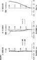
- (A), (B), and (C) in each figure show spherical aberration (sine condition) (LONGITUDINAL SPHERICAL ABERRATION), astigmatism (ASTIGMATISM FIELD CURVES), and distortion aberration (DISTORTION), respectively, in this order.
- the abscissa of the spherical aberration represents the focal position shift in mm, and the ordinate represents the value normalized by the maximum incident height.
- the horizontal axis of astigmatism represents the focal position shift in mm, and the vertical axis represents the image height in mm.
- the horizontal axis of the distortion aberration represents the actual image height as a percentage (%) with respect to the ideal image height, and the vertical axis represents the image height in mm.
- the solid line represents the result for the d line
- the broken line represents the result for the g line.
- the broken line represents the result on the tangential (meridional) surface (M)
- the solid line represents the result on the sagittal (radial) surface (S).
- d-line wavelength 587.56 nm
- g-line wavelength 435.84 nm
- the diagrams of astigmatism and distortion are the results when the d-line (wavelength 587.56 nm) is used.
- transverse aberration diagrams show transverse aberration diagrams (meridional coma).
- (A) and (B) show the case of the maximum image height Y and the case of the 50% image height Y, respectively.
- the horizontal axis represents the entrance pupil position in mm, and the vertical axis represents the lateral aberration.
- the solid line represents the result for the d line, and the broken line represents the result for the g line.
- Tables 1 and 2 show numerical values when the above-described conditional expressions (1) to (6) are applied to the imaging optical systems 1A to 1L of Examples 1 to 12 listed above, respectively.
- the imaging optical systems 1A to 1L in Examples 1 to 12 described above have a five-lens configuration and satisfy the above-described conditions. As a result, the imaging optical systems 1A to 1L are smaller than conventional optical systems. Various aberrations can be corrected more satisfactorily.
- the imaging optical systems 1A to 1L in Examples 1 to 12 are sufficiently reduced in size when mounted on the imaging device 21 and the digital device 3, particularly when mounted on the portable terminal 5.
- a pixel imaging device 18 can be employed.
- a high-pixel image sensor 18 of a class (grade) of about 8M to 16M pixels such as 8M pixel, 10M pixel, and 16M pixel has a short pixel pitch when the size of the image sensor 18 is constant (pixel
- the imaging optical systems 1A to 1L are required to have a resolution corresponding to the pixel pitch, and are defined by, for example, specifications when the imaging optical system 1 is evaluated with the required resolution, for example, with MTF. Although it is necessary to suppress various aberrations within a predetermined range, in the imaging optical systems 1A to 1L in Examples 1 to 12, the various aberrations are suppressed within the predetermined range as shown in each aberration diagram. Accordingly, since the imaging optical systems 1A to 1L in Examples 1 to 12 correct various aberrations satisfactorily, the imaging optical systems 1A to 1L are preferably used for, for example, the imaging element 18 of 8M to 16M pixel class.
- the imaging optical system includes, in order from the object side to the image side, a first lens having a positive refractive power and a biconvex shape, and a second lens having a negative refractive power and having a concave surface facing the image side.
- the third lens is directed from the intersection of the optical axes to the end of the effective region in the contour line of the lens cross section including the optical axis along the optical axis on the object side surface. Inflection points and satisfy the conditional expressions (1) and (2) above.
- Such an imaging optical system is composed of five first to fifth lenses, and each of the first to fifth lenses has the optical characteristics described above, and these five first to fifth lenses are provided.
- this imaging optical system can appropriately arrange the optical power and dispersion with respect to off-axis rays, and better performance up to the peripheral image height. Can be realized.
- the imaging optical system according to another aspect preferably satisfies the conditional expression (3) in the imaging optical system described above.
- the negative refractive power by the so-called air lens constituted by the image side surface of the second lens and the object side surface of the third lens is optimized by satisfying the conditional expression (3).
- the aberration is corrected satisfactorily.
- the imaging optical system according to another aspect preferably satisfies the conditional expression (5) in the imaging optical system described above.
- the shape of the fourth lens is optimized, good off-axis performance is realized regardless of the object distance, and off-axis aberrations are reduced. It is suppressed better.
- the imaging optical system according to another aspect preferably satisfies the conditional expression (6) in the imaging optical system described above.
- the imaging optical system having such a configuration satisfies the conditional expression (6), so that the total length of the imaging optical system is shortened, and the image plane variation with respect to manufacturing errors is reduced.
- the imaging optical system according to another aspect preferably satisfies the conditional expression (7) in the imaging optical system described above.
- the imaging optical system having such a configuration satisfies the conditional expression (7), so that an increase in the total length of the imaging optical system is suppressed, and off-axis aberrations are better suppressed.
- the imaging optical system according to another aspect is preferably the imaging optical system described above, wherein the third lens further has an inflection point on the image side surface.
- the imaging optical system having such a configuration by having the inflection point on the image side surface, the optical power with respect to the off-axis ray is appropriately arranged together with the inflection point on the object side surface of the third lens.
- the field curvature of the off-axis light beam is favorably corrected, which is preferable.
- the fourth lens has an inflection point on at least one of the object side surface and the image side surface.
- an off-axis light beam enters the lens during focusing by having an inflection point on one or both of the object side surface and the image side surface of the fourth lens. Even when the position to be changed changes, it is preferable that the spot position of the off-axis light beam is suppressed from shifting in the optical axis direction.
- the imaging optical system preferably includes a diaphragm on the object side of the first lens in the imaging optical system described above.
- the imaging optical system having such a configuration by disposing the stop on the object side of the first lens, the incident angle of the off-axis light beam with respect to the fifth lens is reduced, and the axis caused by focusing (focusing operation) A favorable telecentric characteristic is realized while a change in the spot position of the outer light beam is suppressed, which is preferable.
- all of the first to fifth lenses are resin material lenses made of a resin material.
- An imaging optical system having such a configuration is formed by resin lenses made by injection molding. Even a lens having a small diameter can be produced in large quantities at a low cost. In addition, since the lens made of resin material can lower the press temperature, it can suppress the wear of the molding die, and as a result, the number of times of replacement and maintenance of the molding die can be reduced, thereby reducing the cost. Can do.
- An image pickup apparatus includes any one of the above-described image pickup optical systems and an image pickup element that converts an optical image into an electrical signal, and the image pickup optical system receives a light receiving surface of the image pickup element.
- An optical image of the object can be formed thereon.
- a digital apparatus includes the above-described imaging device, and a control unit that causes the imaging device to perform at least one of photographing a still image and a moving image of the subject, and imaging optics of the imaging device.
- a system is assembled so that an optical image of the subject can be formed on the imaging surface of the imaging device.
- the digital device comprises a mobile terminal.
- an imaging optical system that is suitably applied to a solid-state imaging device, an imaging device that includes the imaging optical system, and a digital device that includes the imaging device.
Landscapes
- Physics & Mathematics (AREA)
- General Physics & Mathematics (AREA)
- Optics & Photonics (AREA)
- Lenses (AREA)
- Studio Devices (AREA)
Abstract
Le système optique d'imagerie d'après la présente invention est une configuration de cinq lentilles positive, négative, positive, négative et négative. La troisième lentille comporte un point d'inflexion dans la ligne de contour de la coupe transversale de la lentille dans la surface côté objet, en partant du point d'intersection de l'axe de lumière (AX) vers l'extrémité de la zone active. Soit v3 le nombre d'Abbe de la troisième lentille, f la longueur focale de l'ensemble du système et r5 le rayon de courbure paraxial de la surface côté objet de la troisième lentille, les expressions conditionnelles 15 < v3 < 31 et 1 < r5/f < 65 sont satisfaites.
Priority Applications (1)
| Application Number | Priority Date | Filing Date | Title |
|---|---|---|---|
| CN201280025638.XA CN104704415B (zh) | 2011-05-27 | 2012-05-23 | 摄像光学系统、摄像装置以及数字设备 |
Applications Claiming Priority (2)
| Application Number | Priority Date | Filing Date | Title |
|---|---|---|---|
| JP2011118911 | 2011-05-27 | ||
| JP2011-118911 | 2011-05-27 |
Publications (1)
| Publication Number | Publication Date |
|---|---|
| WO2012164877A1 true WO2012164877A1 (fr) | 2012-12-06 |
Family
ID=47258754
Family Applications (1)
| Application Number | Title | Priority Date | Filing Date |
|---|---|---|---|
| PCT/JP2012/003378 WO2012164877A1 (fr) | 2011-05-27 | 2012-05-23 | Système optique d'imagerie, dispositif d'imagerie et appareil numérique |
Country Status (3)
| Country | Link |
|---|---|
| JP (1) | JPWO2012164877A1 (fr) |
| CN (1) | CN104704415B (fr) |
| WO (1) | WO2012164877A1 (fr) |
Cited By (10)
| Publication number | Priority date | Publication date | Assignee | Title |
|---|---|---|---|---|
| JP2013109085A (ja) * | 2011-11-18 | 2013-06-06 | Sony Corp | 撮像レンズおよび撮像装置 |
| WO2014080382A1 (fr) * | 2012-11-26 | 2014-05-30 | Digitaloptics Corporation | Système optique de capture d'image et dispositif de capture d'image l'utilisant |
| JP5513648B1 (ja) * | 2013-03-19 | 2014-06-04 | エーエーシーアコースティックテクノロジーズ(シンセン)カンパニーリミテッド | 撮像レンズ |
| JP5513641B1 (ja) * | 2013-02-20 | 2014-06-04 | 株式会社AAC Technologies Japan R&D Center | 撮像レンズ |
| JP2014130333A (ja) * | 2012-12-28 | 2014-07-10 | Genius Electronic Optical Co | 携帯機器並びにその光学撮像レンズ |
| JP2014197097A (ja) * | 2013-03-29 | 2014-10-16 | 富士フイルム株式会社 | 撮像レンズおよび撮像レンズを備えた撮像装置 |
| JP2015075766A (ja) * | 2013-10-09 | 2015-04-20 | 玉晶光電股▲ふん▼有限公司 | 光学撮像レンズ |
| JP2015087495A (ja) * | 2013-10-30 | 2015-05-07 | コニカミノルタ株式会社 | 撮像レンズ、撮像装置及び携帯端末 |
| JP2015096953A (ja) * | 2013-11-15 | 2015-05-21 | 玉晶光電股▲ふん▼有限公司 | 光学撮像レンズセット |
| JP2017187566A (ja) * | 2016-04-04 | 2017-10-12 | カンタツ株式会社 | 撮像レンズ |
Citations (3)
| Publication number | Priority date | Publication date | Assignee | Title |
|---|---|---|---|---|
| WO2010024198A1 (fr) * | 2008-08-25 | 2010-03-04 | コニカミノルタオプト株式会社 | Objectif d'imagerie, dispositif d'imagerie et terminal portatif |
| JP2010197665A (ja) * | 2009-02-25 | 2010-09-09 | Olympus Corp | 撮像光学系及びそれを備える撮像装置 |
| JP2010224521A (ja) * | 2009-02-27 | 2010-10-07 | Konica Minolta Opto Inc | 撮像レンズ、撮像装置及び携帯端末 |
Family Cites Families (1)
| Publication number | Priority date | Publication date | Assignee | Title |
|---|---|---|---|---|
| JP3544972B1 (ja) * | 2003-12-12 | 2004-07-21 | マイルストーン株式会社 | 撮像レンズ |
-
2012
- 2012-05-23 WO PCT/JP2012/003378 patent/WO2012164877A1/fr active Application Filing
- 2012-05-23 CN CN201280025638.XA patent/CN104704415B/zh active Active
- 2012-05-23 JP JP2013517852A patent/JPWO2012164877A1/ja active Pending
Patent Citations (3)
| Publication number | Priority date | Publication date | Assignee | Title |
|---|---|---|---|---|
| WO2010024198A1 (fr) * | 2008-08-25 | 2010-03-04 | コニカミノルタオプト株式会社 | Objectif d'imagerie, dispositif d'imagerie et terminal portatif |
| JP2010197665A (ja) * | 2009-02-25 | 2010-09-09 | Olympus Corp | 撮像光学系及びそれを備える撮像装置 |
| JP2010224521A (ja) * | 2009-02-27 | 2010-10-07 | Konica Minolta Opto Inc | 撮像レンズ、撮像装置及び携帯端末 |
Cited By (14)
| Publication number | Priority date | Publication date | Assignee | Title |
|---|---|---|---|---|
| JP2013109085A (ja) * | 2011-11-18 | 2013-06-06 | Sony Corp | 撮像レンズおよび撮像装置 |
| WO2014080382A1 (fr) * | 2012-11-26 | 2014-05-30 | Digitaloptics Corporation | Système optique de capture d'image et dispositif de capture d'image l'utilisant |
| JP2014130333A (ja) * | 2012-12-28 | 2014-07-10 | Genius Electronic Optical Co | 携帯機器並びにその光学撮像レンズ |
| JP5513641B1 (ja) * | 2013-02-20 | 2014-06-04 | 株式会社AAC Technologies Japan R&D Center | 撮像レンズ |
| JP2014160154A (ja) * | 2013-02-20 | 2014-09-04 | Aac Technologies Japan R&D Center Ltd | 撮像レンズ |
| JP5513648B1 (ja) * | 2013-03-19 | 2014-06-04 | エーエーシーアコースティックテクノロジーズ(シンセン)カンパニーリミテッド | 撮像レンズ |
| JP2014197097A (ja) * | 2013-03-29 | 2014-10-16 | 富士フイルム株式会社 | 撮像レンズおよび撮像レンズを備えた撮像装置 |
| US9658433B2 (en) | 2013-03-29 | 2017-05-23 | Fujifilm Corporation | Imaging lens and imaging apparatus including the imaging lens |
| US9664880B2 (en) | 2013-03-29 | 2017-05-30 | Fujifilm Corporation | Imaging lens and imaging apparatus including the imaging lens |
| JP2015075766A (ja) * | 2013-10-09 | 2015-04-20 | 玉晶光電股▲ふん▼有限公司 | 光学撮像レンズ |
| US9557527B2 (en) | 2013-10-09 | 2017-01-31 | Genius Electronic Optical, Co., Ltd. | Optical imaging lens and electronic device including the lens |
| JP2015087495A (ja) * | 2013-10-30 | 2015-05-07 | コニカミノルタ株式会社 | 撮像レンズ、撮像装置及び携帯端末 |
| JP2015096953A (ja) * | 2013-11-15 | 2015-05-21 | 玉晶光電股▲ふん▼有限公司 | 光学撮像レンズセット |
| JP2017187566A (ja) * | 2016-04-04 | 2017-10-12 | カンタツ株式会社 | 撮像レンズ |
Also Published As
| Publication number | Publication date |
|---|---|
| CN104704415A (zh) | 2015-06-10 |
| JPWO2012164877A1 (ja) | 2015-02-23 |
| CN104704415B (zh) | 2017-12-05 |
Similar Documents
| Publication | Publication Date | Title |
|---|---|---|
| JP5574049B2 (ja) | 撮像光学系、撮像装置およびデジタル機器 | |
| JP5578275B2 (ja) | 撮像光学系、撮像装置およびデジタル機器 | |
| JP5370619B1 (ja) | 撮像光学系、撮像装置およびデジタル機器 | |
| JP5115647B2 (ja) | 撮像装置およびデジタル機器 | |
| JP5904208B2 (ja) | 撮像レンズ,撮像光学装置及びデジタル機器 | |
| WO2012164877A1 (fr) | Système optique d'imagerie, dispositif d'imagerie et appareil numérique | |
| JP2012203234A (ja) | 撮像光学系、撮像装置およびデジタル機器 | |
| JP5397538B2 (ja) | 撮像レンズ,撮像光学装置及びデジタル機器 | |
| WO2013031122A1 (fr) | Système optique de capture d'image, dispositif de capture d'image et équipement numérique | |
| WO2010140515A1 (fr) | Lentille de capture d'image, dispositif de capture d'image ayant une lentille de capture d'image et terminal portable ayant le dispositif de capture d'image | |
| JP2014123034A (ja) | 撮像光学系、撮像装置およびデジタル機器 | |
| JPWO2009041382A1 (ja) | 広角光学系、撮像レンズ装置、モニタカメラおよびデジタル機器 | |
| WO2013111612A1 (fr) | Objectif de capture d'images | |
| US9547158B2 (en) | Imaging lens and imaging apparatus equipped with the imaging lens | |
| WO2015041123A1 (fr) | Objectif d'imagerie, dispositif d'imagerie et terminal portable | |
| JP2009098492A (ja) | 撮像レンズ、撮像装置およびデジタル機器 | |
| JP2012068292A (ja) | 撮像レンズ、撮像装置及び携帯端末 | |
| JP6287865B2 (ja) | 撮像光学系ならびに撮像装置およびデジタル機器 | |
| WO2012160761A1 (fr) | Optique d'imagerie, appareil d'imagerie et dispositif numérique | |
| WO2012063391A1 (fr) | Système optique de prise d'image, dispositif de prise d'image, et appareil numérique |
Legal Events
| Date | Code | Title | Description |
|---|---|---|---|
| 121 | Ep: the epo has been informed by wipo that ep was designated in this application |
Ref document number: 12793088 Country of ref document: EP Kind code of ref document: A1 |
|
| ENP | Entry into the national phase |
Ref document number: 2013517852 Country of ref document: JP Kind code of ref document: A |
|
| NENP | Non-entry into the national phase |
Ref country code: DE |
|
| 122 | Ep: pct application non-entry in european phase |
Ref document number: 12793088 Country of ref document: EP Kind code of ref document: A1 |