WO2012160663A1 - スピンフィルタ及びその駆動方法 - Google Patents
スピンフィルタ及びその駆動方法 Download PDFInfo
- Publication number
- WO2012160663A1 WO2012160663A1 PCT/JP2011/061958 JP2011061958W WO2012160663A1 WO 2012160663 A1 WO2012160663 A1 WO 2012160663A1 JP 2011061958 W JP2011061958 W JP 2011061958W WO 2012160663 A1 WO2012160663 A1 WO 2012160663A1
- Authority
- WO
- WIPO (PCT)
- Prior art keywords
- spin
- region
- electrode
- energy
- channel region
- Prior art date
- Legal status (The legal status is an assumption and is not a legal conclusion. Google has not performed a legal analysis and makes no representation as to the accuracy of the status listed.)
- Ceased
Links
Images






Classifications
-
- H—ELECTRICITY
- H10—SEMICONDUCTOR DEVICES; ELECTRIC SOLID-STATE DEVICES NOT OTHERWISE PROVIDED FOR
- H10N—ELECTRIC SOLID-STATE DEVICES NOT OTHERWISE PROVIDED FOR
- H10N50/00—Galvanomagnetic devices
- H10N50/80—Constructional details
-
- B—PERFORMING OPERATIONS; TRANSPORTING
- B82—NANOTECHNOLOGY
- B82Y—SPECIFIC USES OR APPLICATIONS OF NANOSTRUCTURES; MEASUREMENT OR ANALYSIS OF NANOSTRUCTURES; MANUFACTURE OR TREATMENT OF NANOSTRUCTURES
- B82Y10/00—Nanotechnology for information processing, storage or transmission, e.g. quantum computing or single electron logic
-
- H—ELECTRICITY
- H10—SEMICONDUCTOR DEVICES; ELECTRIC SOLID-STATE DEVICES NOT OTHERWISE PROVIDED FOR
- H10D—INORGANIC ELECTRIC SEMICONDUCTOR DEVICES
- H10D30/00—Field-effect transistors [FET]
- H10D30/40—FETs having zero-dimensional [0D], one-dimensional [1D] or two-dimensional [2D] charge carrier gas channels
- H10D30/402—Single electron transistors; Coulomb blockade transistors
-
- H—ELECTRICITY
- H10—SEMICONDUCTOR DEVICES; ELECTRIC SOLID-STATE DEVICES NOT OTHERWISE PROVIDED FOR
- H10D—INORGANIC ELECTRIC SEMICONDUCTOR DEVICES
- H10D30/00—Field-effect transistors [FET]
- H10D30/40—FETs having zero-dimensional [0D], one-dimensional [1D] or two-dimensional [2D] charge carrier gas channels
- H10D30/47—FETs having zero-dimensional [0D], one-dimensional [1D] or two-dimensional [2D] charge carrier gas channels having two-dimensional [2D] charge carrier gas channels, e.g. nanoribbon FETs or high electron mobility transistors [HEMT]
- H10D30/471—High electron mobility transistors [HEMT] or high hole mobility transistors [HHMT]
- H10D30/472—High electron mobility transistors [HEMT] or high hole mobility transistors [HHMT] having lower bandgap active layer formed on top of wider bandgap layer, e.g. inverted HEMT
-
- H—ELECTRICITY
- H10—SEMICONDUCTOR DEVICES; ELECTRIC SOLID-STATE DEVICES NOT OTHERWISE PROVIDED FOR
- H10D—INORGANIC ELECTRIC SEMICONDUCTOR DEVICES
- H10D48/00—Individual devices not covered by groups H10D1/00 - H10D44/00
- H10D48/385—Devices using spin-polarised carriers
-
- H—ELECTRICITY
- H10—SEMICONDUCTOR DEVICES; ELECTRIC SOLID-STATE DEVICES NOT OTHERWISE PROVIDED FOR
- H10D—INORGANIC ELECTRIC SEMICONDUCTOR DEVICES
- H10D62/00—Semiconductor bodies, or regions thereof, of devices having potential barriers
- H10D62/80—Semiconductor bodies, or regions thereof, of devices having potential barriers characterised by the materials
- H10D62/83—Semiconductor bodies, or regions thereof, of devices having potential barriers characterised by the materials being Group IV materials, e.g. B-doped Si or undoped Ge
- H10D62/832—Semiconductor bodies, or regions thereof, of devices having potential barriers characterised by the materials being Group IV materials, e.g. B-doped Si or undoped Ge being Group IV materials comprising two or more elements, e.g. SiGe
- H10D62/8325—Silicon carbide
-
- H—ELECTRICITY
- H10—SEMICONDUCTOR DEVICES; ELECTRIC SOLID-STATE DEVICES NOT OTHERWISE PROVIDED FOR
- H10D—INORGANIC ELECTRIC SEMICONDUCTOR DEVICES
- H10D62/00—Semiconductor bodies, or regions thereof, of devices having potential barriers
- H10D62/80—Semiconductor bodies, or regions thereof, of devices having potential barriers characterised by the materials
- H10D62/881—Semiconductor bodies, or regions thereof, of devices having potential barriers characterised by the materials being a two-dimensional material
- H10D62/882—Graphene
-
- H—ELECTRICITY
- H10—SEMICONDUCTOR DEVICES; ELECTRIC SOLID-STATE DEVICES NOT OTHERWISE PROVIDED FOR
- H10D—INORGANIC ELECTRIC SEMICONDUCTOR DEVICES
- H10D64/00—Electrodes of devices having potential barriers
- H10D64/20—Electrodes characterised by their shapes, relative sizes or dispositions
- H10D64/27—Electrodes not carrying the current to be rectified, amplified, oscillated or switched, e.g. gates
- H10D64/311—Gate electrodes for field-effect devices
- H10D64/411—Gate electrodes for field-effect devices for FETs
- H10D64/511—Gate electrodes for field-effect devices for FETs for IGFETs
- H10D64/517—Gate electrodes for field-effect devices for FETs for IGFETs characterised by the conducting layers
- H10D64/519—Gate electrodes for field-effect devices for FETs for IGFETs characterised by the conducting layers characterised by their top-view geometrical layouts
-
- H—ELECTRICITY
- H10—SEMICONDUCTOR DEVICES; ELECTRIC SOLID-STATE DEVICES NOT OTHERWISE PROVIDED FOR
- H10N—ELECTRIC SOLID-STATE DEVICES NOT OTHERWISE PROVIDED FOR
- H10N50/00—Galvanomagnetic devices
- H10N50/01—Manufacture or treatment
Definitions
- the present invention relates to a spin filter using a zigzag graphene ribbon and a driving method thereof.
- CMOS technology using silicon is approaching the limit of miniaturization, and channel alternative materials are being sought for extending its life.
- nanocarbon materials such as carbon nanotubes and graphene are attracting attention, and various research and development are being conducted.
- the spin filter is considered as a basic device in spintronics for obtaining a spin-polarized current.
- a spin filter using even-numbered zigzag graphene nanoribbons having a magnetic moment has been proposed as a spin filter.
- a filter can be formed.
- An object of the present invention is to provide a spin filter that can be easily manufactured. Another object of the present invention is to provide a spin filter driving method capable of selectively conducting either an electron having an up spin or an electron having a down spin.
- the first electrode formed by an even-numbered zigzag graphene ribbon extending in a first direction and having a magnetic moment in a second direction intersecting the first direction;
- a second electrode formed by an even-numbered zigzag graphene ribbon extending in the first direction and having a magnetic moment in the second direction; and disposed between the first electrode and the second electrode And a channel region having an energy level for passing electrons having up spin or electrons having down spin.
- a spin filter driving method wherein the spin filter is formed by an even-numbered zigzag graphene ribbon extending in a first direction and intersects the first direction.
- a channel region disposed between the first electrode and the second electrode and having an energy level that allows an electron having an up spin or an electron having a down spin, and an electric field is applied to the channel region
- the first electrode and the second electrode have an upspin by providing a potential difference between the first electrode and the second electrode.
- a method of driving a spin filter that moves to the first energy region or the second energy region is provided.
- the two electrodes are formed of zigzag graphene ribbons having even-numbered magnetic moments in the same direction. Therefore, the magnetic moment can be easily applied to these electrodes by an external magnetic field or the like.
- either an electron having an up spin or an electron having a down spin can be selected and passed.
- FIG. 1 is a perspective view showing a structure of a spin filter according to an embodiment.
- FIG. 2 is a diagram showing the structure of a zigzag graphene nanoribbon.
- FIG. 3 is a diagram showing a structure in which a source region and a drain region are formed by even-numbered graphene nanoribbons provided with a magnetic moment in the same direction.
- FIG. 4 is a diagram showing the relationship between the spin polarization current and the bias voltage in the structure of FIG.
- FIG. 5 is a diagram showing the relationship between conductance and energy in the structure of FIG.
- FIG. 6 is a diagram showing an energy band structure of the structure of FIG.
- FIG. 7 is a diagram (part 1) for explaining the operation of the structure of FIG. FIG.
- FIG. 8 is a diagram (part 2) for explaining the operation of the structure of FIG.
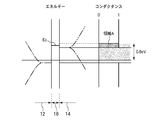
- FIG. 9 is a diagram (part 1) illustrating the operation of the spin filter according to the embodiment.
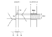
- FIG. 10 is a diagram (part 2) illustrating the operation of the spin filter according to the embodiment.
- FIG. 11 is a diagram illustrating an example of a material forming a channel region of a spin filter according to an embodiment.
- FIG. 12 is a diagram showing the energy band structure of the material forming the channel region of FIG.
- FIG. 13 is a diagram showing a relationship between a spin polarization current and a bias voltage in a spin filter according to an embodiment using the structure of FIG. 11 as a substance forming a channel region.
- FIG. 14 is a diagram (part 1) for explaining the operation of the spin filter according to the embodiment using the structure of FIG. 11 as the material forming the channel region.
- FIG. 15 is a diagram (part 2) for explaining the operation of the spin filter according to the embodiment using the structure of FIG. 11 as the material forming the channel region.
- FIG. 16 is a diagram illustrating another example of the material forming the channel region of the spin filter according to the embodiment.
- FIG. 1 is a perspective view showing the structure of the spin filter according to the present embodiment.
- FIG. 2 is a diagram showing the structure of a zigzag graphene nanoribbon.
- the spin filter according to the present embodiment is disposed between the source region 12 as the first electrode, the drain region 14 as the second electrode, and the source region 12 and the drain region 14.
- Channel region 16 the gate electrode 18 is disposed adjacent to and spaced from the channel region 16.
- the source region 12 and the drain region 14 are formed of even-numbered zigzag graphene nanoribbons having magnetic moments in the same direction.
- the zigzag graphene nanoribbon is a one-dimensional (pseudo one-dimensional) graphene in which carbon atoms at the end of the long side are arranged in a zigzag manner.
- carbon atoms at the end are alternately arranged in a zigzag manner along the X direction. (See the bold line in the figure).
- the even-numbered columns mean that there are even columns of carbon atoms arranged in a zigzag along the X direction in the Y direction.
- the zigzag graphene nanoribbon shown in FIG. 2 shows a case where there are n columns of carbon atoms arranged zigzag along the X direction in the Y direction.
- the even-numbered zigzag graphene nanoribbon is an even-numbered graphene nanoribbon.
- the number of carbon atoms in the zigzag graphene nanoribbon forming the source region 12 and the number of carbon atoms in the zigzag graphene nanoribbon forming the drain region 14 may be the same or different as long as both are even columns. .
- Graphene is known to exhibit different properties from normal graphene by making it into a nano-sized ribbon.
- Graphene having such a structure is called a graphene nanoribbon.
- variety of a graphene nanoribbon corresponds to the graphene ribbon about 100 nm or less, for example.
- the number n of rows of carbon atoms arranged zigzag along the X direction is about 470.
- a graphene ribbon having a nano-order width has characteristics different from those of normal graphene.
- the zigzag graphene nanoribbons in the source region 12 and the drain region 14 have a magnetic moment in a direction perpendicular to the direction in which the graphene ribbon extends (corresponding to the Y direction in FIG. 2).
- the source region 12 and the drain region 14 are arranged so that the directions of magnetic moments are the same (parallel).
- the magnetic moment of the source region 12 and the drain region 14 can be given by an external magnetic field from a ferromagnetic material arranged in the vicinity of the source region 12 and the drain region 14 or by spin injection.
- the channel region 16 is disposed between the source region 12 and the drain region 14 and is made of a material having an energy level in an energy region where only electrons having an up spin pass or in an energy region where only an electron having a down spin passes. Is formed. By forming the channel region 16 with such a substance, electrons having an up spin or electrons having a down spin can be selectively transmitted.
- the material forming the channel region 16 for example, a material having an energy level in the vicinity of the Fermi level (about 1 eV) of the zigzag graphene nanoribbon in the source region 12 and the drain region 14 can be cited.
- the substance forming the channel region 16 will be described in detail in the operation description to be described later.
- the gate electrode 18 is for applying an electric field to the channel region 16 to change the energy level of the channel region 16. Although two gate electrodes 18 are provided so as to sandwich the channel region 16 in FIG. 1, it is not always necessary to provide two, and the gate electrode 18 may be provided only on one side. Further, it is not necessary to provide the gate electrode 18 adjacent to the channel region 16 in plan view, and the gate electrode 18 may be disposed on and / or below the channel region 16. In the case of forming a spin filter that allows only one of electrons having up spin and electrons having down spin to pass, the gate electrode 18 is not necessarily required.
- FIG. 3 is a diagram showing a structure in which a source region and a drain region are formed by even-numbered graphene nanoribbons that are given a magnetic moment in the same direction.
- FIG. 4 is a diagram showing the relationship between the spin polarization current and the bias voltage in the structure of FIG.
- FIG. 5 is a diagram showing the relationship between conductance and energy in the structure of FIG.
- FIG. 6 is a diagram showing an energy band structure of the structure of FIG. 7 and 8 are diagrams for explaining the operation of the structure shown in FIG.
- a structure in which a source region 12, a channel region 16, and a drain region 14 are formed by six rows of zigzag graphene nanoribbons and a magnetic moment in the same direction is applied to the source region 12 and the drain region 14 is assumed. .
- the end of the zigzag graphene nanoribbon is terminated with hydrogen.
- FIG. 4 shows a spin polarization current when a bias voltage V SD is applied between the source region 12 and the drain region 14 in the structure shown in FIG. 3 by using a nonequilibrium Green function method based on the first principle. It is a graph which shows the result of simulation.
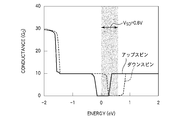
- FIG. 5 is a graph showing the result of simulating the relationship between conductance and energy for the structure shown in FIG. 3 using the nonequilibrium green function method based on the first principle.
- the current value at each bias voltage V SD is obtained by integrating conductance in the energy range corresponding to the bias voltage V SD (corresponding to the shaded portion in FIG. 5).
- the energy region in which the conductance has a finite value varies depending on the spin direction, as shown in FIG. This is because the valence band has an electronic state ( ⁇ state) that is anti-symmetric with respect to the center of the ribbon width, and the conduction band has an electronic state ( ⁇ * state) that is symmetric with respect to the center of the ribbon width. This is due to the electronic state peculiar to even-numbered zigzag graphene nanoribbons.
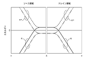
- FIG. 6 is a diagram showing an energy band structure of the structure shown in FIG. In FIG. 6, two band structures assuming the source region 12 and the drain region 14 are drawn symmetrically about the X point.
- the solid line represents the band structure of the down-spin ⁇ state
- the dotted line represents the band structure of the down-spin ⁇ * state
- the one-dot chain line represents the energy band structure of the up-spin ⁇ state
- the two-dot chain line is up It represents the energy band structure of the ⁇ * state of the spin.
- FIG. 7 and 8 are diagrams showing an energy band structure and conductance when a bias voltage V SD of 0.6 V is applied between the source region 12 and the drain region 14.
- FIG. 7 shows the state of an electron having an up spin
- FIG. 8 shows the state of an electron having a down spin. 7 and 8, the channel region 16 is omitted.
- FIG. 9 and 10 are diagrams for explaining the operation of the spin filter according to the present embodiment.
- FIG. 11 is a diagram showing an example of the channel region of the spin filter according to the present embodiment.
- FIG. 12 is a diagram showing the energy band structure of the channel region of FIG.
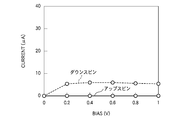
- FIG. 13 is a diagram showing the relationship between the spin polarization current and the bias voltage in the spin filter according to the present embodiment using the channel region of FIG. 14 and 15 are diagrams illustrating the operation of the spin filter according to the present embodiment using the channel region of FIG.
- FIG. 16 is a diagram showing another example of the channel region of the spin filter according to the present embodiment.
- the spin filter according to the present embodiment in order to selectively pass electrons having up spins or electrons having down spins using the above-described characteristics of the structure of FIG. It is formed by such a substance.
- the energy level is either in the energy region where only electrons having up spin pass or in the energy region where only electrons having down spin pass. It is formed with the substance which has this.
- a substance having an energy level Ec in the energy region of the region A and having no energy level in the energy region of the region B is used.
- electrons having a down spin cannot pass through the channel region 16, and only electrons having an up spin can pass through the channel region 16. That is, it functions as a spin filter that passes only electrons with up spin.
- the energy level Ec is included in the energy region of the region B, and the energy is included in the energy region of the region A.
- a substance having no level is used. In this case, electrons having up spin cannot pass through the channel region 16, and only electrons having down spin can pass through the channel region 16. That is, it functions as a spin filter that passes only electrons with down spin.
- the type of spin to be filtered can be changed.
- the channel region 16 is not necessarily required to have a magnetic moment. If the channel region 16 has the energy level Ec in either of the energy regions A and B, the energy levels of the up spin and the down spin are degenerated. It may be.
- the material forming the channel region 16 is not necessarily a material having the energy level Ec in either the energy region of the region A or the region B.
- the energy level Ec of the channel region 16 can be moved into either the energy region of the region A or the region B by the electric field applied to the channel region 16.
- the electric field applied to the channel region 16 can be controlled by the gate voltage Vg applied to the gate electrode 18.
- the channel region 16 does not have a magnetic moment and has a degenerate energy level of both spins. It is assumed that the energy level Ec of the channel region 16 is in the energy region of the region A when no voltage is applied to the gate electrode 18.
- the voltage Vg applied to the gate electrode 18 is about ⁇ 1V.
- the substance forming the channel region 16 is not particularly limited as long as it satisfies the above-described conditions.
- a structure obtained by bending even-numbered graphene nanoribbons can be used as a material for forming such a channel region 16.
- a graphene nanoribbon in a portion between the source region 12 and the drain region 14 can be bent to form a channel region 16.
- FIG. 12 is a graph showing the energy band structure of even-numbered graphene nanoribbons that are bent.
- FIG. 12A shows the state of an electron having an up spin
- FIG. 12B shows the state of an electron having a down spin.
- the structure in which even-numbered graphene nanoribbons are bent has an energy level in which only electrons having a down spin are in a state immediately above the Fermi level, that is, within the energy range of region B. (Refer to the * 1 portion in FIG. 12B).
- FIG. 13 shows a simulation of the spin polarization current when a bias voltage V SD is applied between the source region 12 and the drain region 14 in the structure shown in FIG. 11, using the nonequilibrium green function method based on the first principle. It is a graph which shows the result.
- the number of energy levels applied to the energy region of the region B is changed by the voltage applied to the gate electrode 18. be able to.
- the magnitude of the spin polarization current flowing between the source region 12 and the drain region 14 can be changed. That is, the magnitude of the spin polarization current can be controlled by the voltage applied to the gate electrode 18.
- Energy level Ec 2 of electrons with spin-up is, for example, ⁇ 2 of the energy levels shown in FIG. 12 (a) corresponds.
- the width between the even-numbered graphene nanoribbons forming the source region 12 and the even-numbered graphene nanoribbons forming the drain region 14 is narrower than the width of the carbon single atom or graphene nanoribbon.
- the connection may be made by the channel region 16 of the ribbon.
- Single atoms and thin ribbons are degenerated by two spins and appear near the Fermi level of the graphene nanoribbons that form the source region 12 and the drain region 14.
- a silicon carbide (SiC) film is formed on the substrate 10, and heat treatment is performed at a temperature of 1350 ° C., for example. Thereby, silicon on the surface of the silicon carbide film evaporates, and a single layer of graphene sheet is formed on the surface of the silicon carbide film.
- the atomic arrangement of the graphene sheet can be determined by controlling the crystal orientation of silicon carbide.
- a graphene sheet is synthesized by a CVD method using a catalytic metal such as cobalt (Co), nickel (Ni), iron (Fe), copper (Cu), and the synthesized graphene sheet is transferred onto the substrate 10. May be.
- the atomic arrangement of the graphene sheet can be confirmed using an electron microscope or a scanning microscope.
- a resist is applied on the graphene sheet formed on the substrate 10, and the resist is patterned into the shape of the source region 12, the drain region 14, the channel region 16, and the gate electrode 18 by photolithography or electron beam lithography.
- the graphene sheet is patterned by reactive ion etching using oxygen (O 2 ) gas, milling using argon (Ar) gas, or the like.
- oxygen (O 2 ) gas oxygen
- Ar argon
- a metal electrode such as a titanium (Ti) film or a gold (Au) film is formed on the patterned source region 12 and drain region 14 as necessary.
- a ferromagnetic material that gives a magnetic moment to the graphene nanoribbons in the source region 12 and the drain region 14 is formed in the vicinity of the source region 12 and the drain region 14.
- the ferromagnetic material may be in direct contact with the source region 12 and the drain region 14, or the metal electrode material itself may be a ferromagnetic material.
- the ferromagnetic material does not necessarily need to be in direct contact with the source region 12 and the drain region 14, and may be formed at a location separated from the source region 12 and the drain region 14.
- the magnetization direction of the ferromagnetic material may be one direction. Therefore, the ferromagnetic material can be easily magnetized by using an external magnetic field or the like.
- the source region and the drain region are formed by the even-numbered zigzag graphene ribbon having the magnetic moment in the same direction, so that the magnetic moment can be easily given to these electrodes by an external magnetic field or the like. Can do. Further, by applying an electric field to the channel region to move the energy level of the channel region, either an electron having an up spin or an electron having a down spin can be selected and passed.
- the source region and the drain region are disposed adjacent to the extending direction of the graphene nanoribbon, but the source region and the drain region are not necessarily disposed adjacent to the extending direction of the graphene nanoribbon.
- a graphene nanoribbon that forms a source region and a graphene nanoribbon that forms a drain region may be arranged in parallel.
- the channel region may be drawn from the short side of the graphene nanoribbon, or may be drawn from the long side of the graphene nanoribbon.
- the channel region has only one energy level, but the channel region may have a plurality of energy levels.
- the channel region may have a plurality of energy levels.
- the spin filter has been described.
- a spin switch or a spin transistor may be formed using a similar structure.
- constituent materials and manufacturing conditions disclosed in the above embodiment are not limited to the disclosed contents, and can be appropriately changed according to the purpose and the like.
Landscapes
- Engineering & Computer Science (AREA)
- Chemical & Material Sciences (AREA)
- Nanotechnology (AREA)
- Physics & Mathematics (AREA)
- Mathematical Physics (AREA)
- Theoretical Computer Science (AREA)
- Crystallography & Structural Chemistry (AREA)
- Manufacturing & Machinery (AREA)
- Hall/Mr Elements (AREA)
- Thin Film Transistor (AREA)
Abstract
第1の方向に延在する偶数列のジグザググラフェンリボンにより形成され、第1の方向と交差する第2の方向の磁気モーメントを有する第1の電極と、第1の方向に延在する偶数列のジグザググラフェンリボンにより形成され、第2の方向の磁気モーメントを有する第2の電極と、第1の電極と第2の電極との間に配置され、アップスピンをもつ電子又はダウンスピンをもつ電子を通過させるエネルギー準位を有するチャネル領域とを有する。
Description
本発明は、ジグザググラフェンリボンを用いたスピンフィルタ及びその駆動方法に関する。
シリコンを利用したCMOS技術は微細化の限界に近づきつつあり、その寿命を延ばすためのチャネル代替材料が模索されている。その最有力候補として、カーボンナノチューブやグラフェンを代表とするナノカーボン材料が注目されており、種々の研究・開発が行われている。
ナノカーボン材料の研究・開発を通して、スピントロニクスなどのCMOS技術を超えた技術に繋がる新しい情報処理概念の発見がなされることが期待されている。これまでにも実際、カーボンナノチューブやグラフェンへの室温でのスピン注入や数μmの長いスピン緩和など、スピントロニクス材料に適した種々の性質が観測されている。
スピンフィルタは、スピン分極した電流を得るためのスピントロニクスにおける基礎デバイスと考えられている。近年、スピンフィルタとして、磁気モーメントをもつ偶数列のジグザググラフェンナノリボンを利用したスピンフィルタが提案されている。磁気モーメントをもつ偶数列のジグザググラフェンナノリボンにより2つの電極を形成し、これら電極の磁気モーメントの向きを互いに反平行にすることにより、一方の向きのスピンをもつ電子だけが伝導することのできるスピンフィルタを形成することができる。
Taisuke Ozaki et al., "Dual spin filter effect in a zigzag graphene nanoribbon", Physical Review B 81, 074522, 2010
Chuanhong Jin et al., "Deriving carbon atomic chains from graphene", Physical Review Letters 102, 205501, 2009
Jinming Cai et al., "Atomically precise bottom-up fabrication of graphene nanoribbons", Nature, Vol. 466, July 22, 2010
しかしながら、上記従来のスピンフィルタにおいては、2つの電極に逆向きの磁気モーメントを与えることが必要であり、製造が容易でないことが想像される。また、スピンフィルタとしての利用性を向上するためには、アップスピンをもつ電子及びダウンスピンをもつ電子のいずれかを任意に選択して伝導できることが望ましい。
本発明の目的は、容易に製造しうるスピンフィルタを提供することにある。また、本発明の他の目的は、アップスピンをもつ電子及びダウンスピンをもつ電子のいずれかを選択して伝導しうるスピンフィルタの駆動方法を提供することにある。
実施形態の一観点によれば、第1の方向に延在する偶数列のジグザググラフェンリボンにより形成され、第1の方向と交差する第2の方向の磁気モーメントを有する第1の電極と、前記第1の方向に延在する偶数列のジグザググラフェンリボンにより形成され、前記第2の方向の磁気モーメントを有する第2の電極と、前記第1の電極と前記第2の電極との間に配置され、アップスピンをもつ電子又はダウンスピンをもつ電子を通過させるエネルギー準位を有するチャネル領域とを有するスピンフィルタが提供される。
また、実施形態の他の観点によれば、スピンフィルタの駆動方法であって、前記スピンフィルタは、第1の方向に延在する偶数列のジグザググラフェンリボンにより形成され、第1の方向と交差する第2の方向の磁気モーメントを有する第1の電極と、前記第1の方向に延在する偶数列のジグザググラフェンリボンにより形成され、前記第2の方向の磁気モーメントを有する第2の電極と、前記第1の電極と前記第2の電極との間に配置され、アップスピンをもつ電子又はダウンスピンをもつ電子を許容するエネルギー準位を有するチャネル領域と、前記チャネル領域に電界を印加するゲート電極とを有し、前記第1の電極と前記第2の電極との間に電位差を与えることにより、前記第1の電極及び前記第2の電極に、アップスピンをもつ電子だけが通過する第1のエネルギー領域と、ダウンスピンをもつ電子だけが通過する第2のエネルギー領域とを形成し、前記ゲート電極に印加する電圧により、前記チャネル領域の前記エネルギー準位を、前記第1のエネルギー領域又は前記第2のエネルギー領域に移動するスピンフィルタの駆動方法が提供される。
開示のスピンフィルタによれば、2つの電極を同じ方向の磁気モーメントを有する偶数列のジグザググラフェンリボンにより形成するので、外部磁場等によってこれら電極に容易に磁気モーメントを与えることができる。
また、開示のスピンフィルタの駆動方法によれば、アップスピンをもつ電子及びダウンスピンをもつ電子のいずれかを選択して通過させることができる。
一実施形態によるスピンフィルタ及びその製造方法について図1乃至図16を用いて説明する。
はじめに、本実施形態によるスピンフィルタの構造について図1及び図2を用いて説明する。図1は、本実施形態によるスピンフィルタの構造を示す斜視図である。図2は、ジグザググラフェンナノリボンの構造を示す図である。
本実施形態によるスピンフィルタは、図1に示すように、第1の電極としてのソース領域12と、第2の電極としてのドレイン領域14と、ソース領域12とドレイン領域14との間に配置されたチャネル領域16とを有している。また、チャネル領域16から離間して隣接配置されたゲート電極18を有している。
ソース領域12及びドレイン領域14は、互いに同じ方向の磁気モーメントをもつ偶数列のジグザググラフェンナノリボンにより形成されている。
ジグザググラフェンナノリボンとは、長辺端部の炭素原子がジグザグに配列された1次元状(擬1次元)のグラフェンである。例えば図2に示すように、X方向に延在する1次元状のグラフェンにおいて、端部(図中、点線で囲った領域を参照)の炭素原子がX方向に沿って交互にジグザグに配置されたものである(図中、太線を参照)。
偶数列とは、X方向に沿ってジグザグに配置された炭素原子の列が、Y方向に偶数列存在することを意味する。図2に示すジグザググラフェンナノリボンは、X方向に沿ってジグザグに配置された炭素原子の列が、Y方向にn列存在する場合を示している。偶数列のジグザググラフェンナノリボンは、nが偶数のグラフェンナノリボンである。ソース領域12を形成するジグザググラフェンナノリボンにおける炭素原子の列数と、ドレイン領域14を形成するジグザググラフェンナノリボンにおける炭素原子の列数とは、いずれも偶数列であれば、同じでも異なっていてもよい。
グラフェンは、ナノサイズのリボン状にすることによって通常のグラフェンとは異なる性質を発現することが知られている。このような構造のグラフェンが、グラフェンナノリボンと呼ばれている。グラフェンナノリボンの幅について特に定義はないが、例えばY方向の幅が100nm程度以下のグラフェンリボンが該当する。幅100nmのグラフェンリボンの場合、X方向に沿ってジグザグに配置された炭素原子の列の数nが約470程度となる。ナノオーダーの幅を有するグラフェンリボンは、通常のグラフェンとは異なる特性を有している。
ソース領域12及びドレイン領域14のジグザググラフェンナノリボンは、グラフェンリボンの延在する方向と垂直な方向(図2のY方向に相当)の磁気モーメントを有している。ソース領域12とドレイン領域14とは、磁気モーメントの向きが同じ(平行)になるように配置される。
ソース領域12及びドレイン領域14の磁気モーメントは、ソース領域12及びドレイン領域14の近傍に配置された強磁性体からの外部磁場により、或いは、スピン注入などにより与えることができる。
チャネル領域16は、ソース領域12とドレイン領域14との間に配置され、アップスピンをもつ電子だけが通過するエネルギー領域又はダウンスピンをもつ電子だけが通過するエネルギー領域にエネルギー準位を有する物質により形成されている。このような物質によりチャネル領域16を形成することにより、アップスピンをもつ電子又はダウンスピンをもつ電子を選択的に通過させることができる。
チャネル領域16を形成する物質の一例としては、例えば、ソース領域12及びドレイン領域14のジグザググラフェンナノリボンのフェルミ準位付近(~1eV程度)にエネルギー準位を有する物質が挙げられる。なお、チャネル領域16を形成する物質については、後述する動作説明のなかで詳しく説明する。
ゲート電極18は、チャネル領域16に電界を加えてチャネル領域16のエネルギー準位を変化するためのものである。図1ではチャネル領域16を挟むように2つのゲート電極18を設けているが、必ずしも2つ設ける必要はなく、一方の側のみにゲート電極18を設けるようにしてもよい。また、平面的に見てチャネル領域16に隣接してゲート電極18を設ける必要はなく、チャネル領域16の上及び/又は下にゲート電極18を配置するようにしてもよい。アップスピンをもつ電子又はダウンスピンをもつ電子のいずれか一方のみを通過させるスピンフィルタを形成する場合にあっては、必ずしもゲート電極18は必要ではない。
次に、同じ方向の磁気モーメントをもつソース領域12及びドレイン領域14を接合したときの基本的な動作について、図3乃至図8を用いて説明する。
図3は、同じ方向の磁気モーメントを与えた偶数列のグラフェンナノリボンによりソース領域及びドレイン領域を形成した構造体を示す図である。図4は、図3の構造体におけるスピン分極電流とバイアス電圧との関係を示す図である。図5は、図3の構造体におけるコンダクタンスとエネルギーとの関係を示す図である。図6は、図3の構造体のエネルギーバンド構造を示す図である。図7及び図8は、図3の構造体の動作を説明する図である。
図3に示すように、6列のジグザググラフェンナノリボンによってソース領域12、チャネル領域16及びドレイン領域14を形成し、ソース領域12及びドレイン領域14に同じ方向の磁気モーメントを与えた構造体を想定する。ジグザググラフェンナノリボンの端部は、水素により終端されているものとする。
図4は、図3に示す構造体について、ソース領域12とドレイン領域14との間にバイアス電圧VSDを印加したときのスピン分極電流を、第一原理に基づく非平衡グリーン関数法を用いてシミュレーションした結果を示すグラフである。また、図5は、図3に示す構造体について、コンダクタンスとエネルギーとの関係を、第一原理に基づく非平衡グリーン関数法を用いてシミュレーションした結果を示すグラフである。
図4に示すように、ソース領域12とドレイン領域14との間にバイアス電圧VSDを印加すると、ソース領域12とドレイン領域14との間を、アップスピンをもつ電子とダウンスピンをもつ電子の双方が伝導する。すなわち、図3に示す構造体は、スピンフィルタとしては機能しない。
しかしながら、各バイアス電圧VSDにおける電流値は、バイアス電圧VSDに相当するエネルギー範囲(図5の網掛け部分に相当)においてコンダクタンスを積分したものである。コンダクタンスが有限の値をもつエネルギー領域は、図5に示すように、スピンの向きによって異なっている。これは、価電子帯はリボンの幅の中心に対して反対称な電子状態(π状態)を有し、伝導帯はリボンの幅の中心に対して対称な電子状態(π*状態)を有するという、偶数列ジグザググラフェンナノリボンに特有の電子状態に起因するものである。
図6は、図3に示す構造体のエネルギーバンド構造を示す図である。図6では、ソース領域12及びドレイン領域14を想定した2つのバンド構造を、X点を中心にして対称に描いている。
図中、実線はダウンスピンのπ状態のバンド構造を表し、点線はダウンスピンのπ*状態のバンド構造を表し、一点鎖線はアップスピンのπ状態のエネルギーバンド構造を表し、二点鎖線はアップスピンのπ*状態のエネルギーバンド構造を表している。
図6に示すように、図3に示す構造体のエネルギーバンドは、フェルミ準位(エネルギー=0)近傍において交換分裂し、アップスピンバンドのエネルギーがダウンスピンバンドのエネルギーよりも低くなっている。
図7及び図8は、ソース領域12とドレイン領域14との間に0.6Vのバイアス電圧VSDを印加したときのエネルギーバンド構造及びコンダクタンスを示す図である。図7はアップスピンをもつ電子の状態を示し、図8はダウンスピンをもつ電子の状態を示している。なお、図7及び図8では、チャネル領域16を省略している。
ソース領域12及びドレイン領域14がアップスピンの向きに磁気モーメントをもつ場合、図7に示すように、積分範囲(図中、網掛け部分)の高エネルギー側にアップスピンをもつ電子だけが通過するエネルギー領域(図中、領域A)が現れる。また、積分範囲(図中、網掛け部分)の低エネルギー側には、図8に示すように、ダウンスピンをもつ電子だけが通過するエネルギー領域(図中、領域B)が現れる。磁気モーメントが逆向きの場合は、領域Aを通過するスピンの向きと領域Bを通過するスピンの向きとの関係が上記とは逆になる。
次に、本実施形態によるスピンフィルタの動作について図9乃至図16を用いて説明する。
図9及び図10は、本実施形態によるスピンフィルタの動作を説明する図である。図11は、本実施形態によるスピンフィルタのチャネル領域の一例を示す図である。図12は、図11のチャネル領域のエネルギーバンド構造を示す図である。図13は、図11のチャネル領域を用いた本実施形態によるスピンフィルタにおけるスピン分極電流とバイアス電圧との関係を示す図である。図14及び図15は、図11のチャネル領域を用いた本実施形態によるスピンフィルタの動作を説明する図である。図16は、本実施形態によるスピンフィルタのチャネル領域の他の例を示す図である。
本実施形態によるスピンフィルタでは、図3の構造体が有する上述のような特性を利用してアップスピンをもつ電子又はダウンスピンをもつ電子を選択的に通過させるために、チャネル領域16を以下のような物質により形成する。
すなわち、本実施形態によるスピンフィルタでは、チャネル領域16を形成する物質として、アップスピンをもつ電子だけが通過するエネルギー領域又はダウンスピンをもつ電子だけが通過するエネルギー領域のいずれか一方にエネルギー準位を有する物質により形成する。
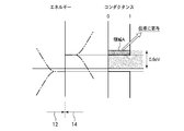
例えば図9に示すように、領域Aのエネルギー領域内にエネルギー準位Ecを有し、領域Bのエネルギー領域内にエネルギー準位をもたない物質を用いる。この場合、ダウンスピンをもつ電子はチャネル領域16を通過できず、アップスピンをもつ電子だけがチャネル領域16を通過することができる。つまり、アップスピンをもつ電子だけを通過するスピンフィルタとして機能する。
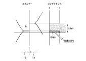
或いは、本実施形態によるスピンフィルタでは、チャネル領域16を形成する物質として、例えば図10に示すように、領域Bのエネルギー領域内にエネルギー準位Ecを有し、領域Aのエネルギー領域内にエネルギー準位をもたない物質を用いる。この場合、アップスピンをもつ電子はチャネル領域16を通過できず、ダウンスピンをもつ電子だけがチャネル領域16を通過することができる。つまり、ダウンスピンをもつ電子だけを通過するスピンフィルタとして機能する。
このようにしてチャネル領域16を形成する物質を変えることにより、フィルタリングするスピンの種類を変えることができる。
チャネル領域16は、必ずしも磁気モーメントをもつ必要はなく、領域A又は領域Bのいずれかのエネルギー領域内にエネルギー準位Ecを有するものであれば、アップスピンとダウンスピンのエネルギー準位が縮退していてもよい。
チャネル領域16を形成する物質は、必ずしも領域A又は領域Bのいずれかのエネルギー領域内にエネルギー準位Ecを有する物質である必要はない。チャネル領域16に印加する電界により、チャネル領域16のエネルギー準位Ecを領域A又は領域Bのいずれかのエネルギー領域内に移動することもできる。チャネル領域16に印加する電界は、ゲート電極18に印加するゲート電圧Vgによって制御することができる。
また、ゲート電極18に印加するゲート電圧Vgを適宜制御することにより、アップスピンをもつ電子又はダウンスピンをもつ電子のいずれかを選択的に通過させることも可能である。
例えば、チャネル領域16として、磁気モーメントをもたず、両スピンのエネルギー準位が縮退している状態の物質を想定する。ゲート電極18に電圧を印加しないとき、チャネル領域16のエネルギー準位Ecが領域Aのエネルギー領域内にあるものとする。
このような場合、ゲート電極18にゲート電圧Vgを印加しない状態では、アップスピンをもつ電子だけが通過するスピンフィルタとして機能する(図9参照)。一方、ゲート電極18にゲート電圧Vgを印加してチャネル領域16のエネルギー準位を領域Bのエネルギー範囲内まで押し下げることにより、ダウンスピンをもつ電子だけが通過するスピンフィルタとして機能する(図10参照)。
なお、一般的な電子デバイスの動作電圧を考慮すると、ゲート電極18に印加する電圧Vgが±1V程度であることが望ましい。
このように、ゲート電極18に印加するゲート電圧により、アップスピンをもつ電子又はダウンスピンをもつ電子のいずれかを選択的に通過するスピンフィルタとなる。
チャネル領域16を形成する物質は、上述の条件を満たす物質であれば、特に限定されるものではない。
このようなチャネル領域16を形成する物質としては、例えば、偶数列のグラフェンナノリボンを屈曲した構造体を用いることができる。例えば図11に示すように、ソース領域12とドレイン領域14との間の部分のグラフェンナノリボンを折り曲げてチャネル領域16とすることができる。
図12は、折り曲げた偶数列のグラフェンナノリボンのエネルギーバンド構造を示すグラフである。図12(a)がアップスピンをもつ電子の状態を示し、図12(b)がダウンスピンをもつ電子の状態を示している。
図12に示すように、偶数列のグラフェンナノリボンを屈曲した構造体は、フェルミ準位直上に、すなわち領域Bのエネルギー範囲内に、ダウンスピンをもつ電子だけが状態をもつエネルギー準位を有している(図12(b)の※1部分を参照)。
図13は、図11に示す構造体においてソース領域12とドレイン領域14との間にバイアス電圧VSDを印加したときのスピン分極電流を、第一原理に基づく非平衡グリーン関数法を用いてシミュレーションした結果を示すグラフである。
チャネル領域16として偶数列のグラフェンナノリボンを屈曲した構造体は、図13に示すように、ダウンスピンをもつ電子を通過するが、アップスピンをもつ電子を通過しない。すなわち、ダウンスピンをもつ電子だけが通過するスピンフィルタを実現できることが検証できた。これは、図14に示すように、ダウンスピンをもつ電子のエネルギー準位Ec1が、領域Bのエネルギー範囲に位置しているためである。
また、図12(b)の※1部分に示すように近傍に複数のエネルギー準位が存在する場合、ゲート電極18に印加する電圧によって、領域Bのエネルギー領域にかかるエネルギー準位の数を変えることができる。これにより、ソース領域12とドレイン領域14との間に流れるスピン分極電流の大きさを変化することができる。すなわち、ゲート電極18に印加する電圧により、スピン分極電流の大きさを制御することができる。
また、ゲート電極18に電圧を印加してチャネル領域16のエネルギー準位を押し下げると、ダウンスピンの状態は領域Bから離れ、逆にアップスピンをもつ電子のエネルギー準位Ec2が領域Aに入るため、アップスピンをもつ電子だけが通過するスピンフィルタを実現することができる。アップスピンをもつ電子のエネルギー準位Ec2は、例えば図12(a)の※2部分のエネルギー準位が該当する。
或いは、例えば図16に示すように、ソース領域12を形成する偶数列のグラフェンナノリボンとドレイン領域14を形成する偶数列のグラフェンナノリボンとの間を、炭素単原子又はグラフェンナノリボンの幅より幅の細いリボンのチャネル領域16により接続するようにしてもよい。
単原子や細いリボンでは、2つのスピンで縮退しており、ソース領域12及びドレイン領域14を形成するグラフェンナノリボンのフェルミ準位近傍に現れる。
この場合、チャネル領域16のエネルギー準位が領域Bのエネルギー範囲内となる小さいゲート電圧Vgを印加することにより、ダウンスピンだけが通過するスピンフィルタを実現できる。また、チャネル領域16のエネルギー準位が領域Aのエネルギー範囲内となる大きいゲート電圧Vgを印加することにより、アップスピンだけが通過するスピンフィルタを実現できる。
次に、本実施形態によるスピンフィルタの製造方法について図1を参照して説明する。
まず、基板10上に、シリコンカーバイド(SiC)膜を形成し、例えば1350℃の温度で熱処理を行う。これにより、シリコンカーバイド膜の表面のシリコンが蒸発し、シリコンカーバイド膜の表面に1層のグラフェンシートが形成される。グラフェンシートの原子配列は、シリコンカーバイドの結晶方位を制御することにより、決定することができる。
或いは、コバルト(Co)、ニッケル(Ni)、鉄(Fe)、銅(Cu)等の触媒金属を利用したCVD法によりグラフェンシートを合成し、基板10上に合成したグラフェンシートを転写するようにしてもよい。グラフェンシートの原子配列は、電子顕微鏡や走査顕微鏡を用いて確認することができる。
次いで、基板10に形成したグラフェンシート上に、レジストを塗布し、フォトリソグラフィや電子線リソグラフィにより、ソース領域12、ドレイン領域14、チャネル領域16及びゲート電極18の形状にレジストをパターニングする。
次いで、このレジストをマスクとして、酸素(O2)ガスを用いた反応性イオンエッチングやアルゴン(Ar)ガスを用いたミリング等によりグラフェンシートをパターニングする。こうして、偶数列のグラフェンナノリボンのソース領域12及びドレイン領域14、チャネル領域16、並びにゲート電極18を形成する。
次いで、必要に応じて、パターニングしたソース領域12及びドレイン領域14上に、チタン(Ti)膜や金(Au)膜等の金属電極を形成する。
次いで、ソース領域12及びドレイン領域14近傍に、ソース領域12及びドレイン領域14のグラフェンナノリボンに磁気モーメントを与える強磁性体を形成する。
この強磁性体は、ソース領域12及びドレイン領域14に直に接するようにしてもよいし、金属電極の材料自体を強磁性体としてもよい。また、強磁性体は、必ずしもソース領域12及びドレイン領域14に直に接している必要はなく、ソース領域12及びドレイン領域14から離間した場所に形成してもよい。
本実施形態によるスピンフィルタでは、ソース領域12及びドレイン領域14に与える磁気モーメントが同じ方向であるため、強磁性体の磁化方向は一方向でよい。したがって、外部磁場等を利用することにより、強磁性体を容易に磁化することができる。
ソース領域12及びドレイン領域14のグラフェンナノリボンへの磁気モーメントの付与には、スピン注入等の他の方法を用いてもよい。
このように、本実施形態によれば、ソース領域及びドレイン領域を、同じ方向の磁気モーメントを有する偶数列のジグザググラフェンリボンにより形成するので、外部磁場等によってこれら電極に容易に磁気モーメントを与えることができる。また、チャネル領域に電界を印加してチャネル領域のエネルギー準位を移動させることにより、アップスピンをもつ電子及びダウンスピンをもつ電子のいずれかを選択して通過させることができる。
[変形実施形態]
上記実施形態に限らず種々の変形が可能である。
上記実施形態に限らず種々の変形が可能である。
例えば、上記実施形態では、グラフェンナノリボンの延在する方向に隣接してソース領域及びドレイン領域を配置したが、ソース領域とドレイン領域は、必ずしもグラフェンナノリボンの延在する方向に隣接配置する必要はない。
例えば、ソース領域を形成するグラフェンナノリボンとドレイン領域を形成するグラフェンナノリボンとを平行に配置してもよい。この場合、チャネル領域は、グラフェンナノリボンの短辺から引き出すようにしてもよいし、グラフェンナノリボンの長辺から引き出すようにしてもよい。
また、上記実施形態では、チャネル領域が一つのエネルギー準位のみを有するように説明した部分があるが、チャネル領域は、複数のエネルギー準位を有してもよい。領域Aのエネルギー領域にアップスピンをもつ電子を許容するエネルギー準位が存在する場合に、領域Bのエネルギー領域にダウンスピンをもつ電子を許容するエネルギー準位が1つも存在しなければよい。また、領域Bのエネルギー領域にダウンスピンをもつ電子を許容するエネルギー準位が存在する場合には、領域Aのエネルギー領域にアップスピンをもつ電子を許容するエネルギー準位が1つも存在しなければよい。
また、上記実施形態ではスピンフィルタについて説明したが、同様の構造体により、スピンスイッチやスピントランジスタを形成するようにしてもよい。
また、上記実施形態に開示の構成材料や製造条件は、当該開示内容に限定されるものではなく、目的等に応じて適宜変更が可能である。
10…基板
12…ソース領域
14…ドレイン領域
16…チャネル領域
18…ゲート電極
12…ソース領域
14…ドレイン領域
16…チャネル領域
18…ゲート電極
Claims (14)
- 第1の方向に延在する偶数列のジグザググラフェンリボンにより形成され、第1の方向と交差する第2の方向の磁気モーメントを有する第1の電極と、
前記第1の方向に延在する偶数列のジグザググラフェンリボンにより形成され、前記第2の方向の磁気モーメントを有する第2の電極と、
前記第1の電極と前記第2の電極との間に配置され、アップスピンをもつ電子又はダウンスピンをもつ電子を通過させるエネルギー準位を有するチャネル領域と
を有することを特徴とするスピンフィルタ。 - 請求項1記載のスピンフィルタにおいて、
前記第1の電極と前記第2の電極との間に電位差を与えることにより、前記第1の電極及び前記第2の電極に、アップスピンをもつ電子だけが通過する第1のエネルギー領域と、ダウンスピンをもつ電子だけが通過する第2のエネルギー領域とが形成され、
前記チャネル領域は、前記第1のエネルギー領域に、アップスピンをもつ電子を許容する前記エネルギー準位を有する
ことを特徴とするスピンフィルタ。 - 請求項2記載のスピンフィルタにおいて、
前記チャネル領域に電界を印加するゲート電極を更に有し、
前記チャネル領域の前記エネルギー準位は、前記ゲート電極に印加する電圧により、前記第1のエネルギー領域に移動されている
ことを特徴とするスピンフィルタ。 - 請求項1記載のスピンフィルタにおいて、
前記第1の電極と前記第2の電極との間に電位差を与えることにより、前記第1の電極及び前記第2の電極に、アップスピンをもつ電子だけが通過する第1のエネルギー領域と、ダウンスピンをもつ電子だけが通過する第2のエネルギー領域とが形成され、
前記チャネル領域は、前記第2のエネルギー領域に、ダウンスピンをもつ電子を許容する前記エネルギー準位を有する
ことを特徴とするスピンフィルタ。 - 請求項4記載のスピンフィルタにおいて、
前記チャネル領域に電界を印加するゲート電極を更に有し、
前記チャネル領域の前記エネルギー準位は、前記ゲート電極に印加する電圧により、前記第2のエネルギー領域に移動されている
ことを特徴とするスピンフィルタ。 - 請求項1記載のスピンフィルタにおいて、
前記チャネル領域に電界を印加するゲート電極を更に有し、
前記第1の電極と前記第2の電極との間に電位差を与えることにより、前記第1の電極及び前記第2の電極に、アップスピンをもつ電子だけが通過する第1のエネルギー領域と、ダウンスピンをもつ電子だけが通過する第2のエネルギー領域とが形成され、
前記チャネル領域の前記エネルギー準位は、前記ゲート電極に印加する電圧により、前記第1のエネルギー領域又は前記第2のエネルギー領域に移動されている
ことを特徴とするスピンフィルタ。 - 請求項1乃至6のいずれか1項に記載のスピンフィルタにおいて、
前記チャネル領域は、アップスピンをもつ電子及びダウンスピンをもつ電子の双方を許容する前記エネルギー準位を有する
ことを特徴とするスピンフィルタ。 - 請求項1乃至7のいずれか1項に記載のスピンフィルタにおいて、
前記チャネル領域は、偶数列のジグザググラフェンリボンを屈曲することにより形成されている
ことを特徴とするスピンフィルタ。 - 請求項1乃至8のいずれか1項に記載のスピンフィルタにおいて、
前記チャネル領域は、炭素単原子により形成されている
ことを特徴とするスピンフィルタ。 - 請求項1乃至8のいずれか1項に記載のスピンフィルタにおいて、
前記チャネル領域は、前記第1の電極及び前記第2の電極を形成する前記ジグザググラフェンリボンよりも細いジグザググラフェンリボンにより形成されている
ことを特徴とするスピンフィルタ。 - スピンフィルタの駆動方法であって、
前記スピンフィルタは、第1の方向に延在する偶数列のジグザググラフェンリボンにより形成され、第1の方向と交差する第2の方向の磁気モーメントを有する第1の電極と、前記第1の方向に延在する偶数列のジグザググラフェンリボンにより形成され、前記第2の方向の磁気モーメントを有する第2の電極と、前記第1の電極と前記第2の電極との間に配置され、アップスピンをもつ電子又はダウンスピンをもつ電子を許容するエネルギー準位を有するチャネル領域と、前記チャネル領域に電界を印加するゲート電極とを有し、
前記第1の電極と前記第2の電極との間に電位差を与えることにより、前記第1の電極及び前記第2の電極に、アップスピンをもつ電子だけが通過する第1のエネルギー領域と、ダウンスピンをもつ電子だけが通過する第2のエネルギー領域とを形成し、
前記ゲート電極に印加する電圧により、前記チャネル領域の前記エネルギー準位を、前記第1のエネルギー領域又は前記第2のエネルギー領域に移動する
ことを特徴とするスピンフィルタの駆動方法。 - 請求項11記載のスピンフィルタの駆動方法において、
前記チャネル領域は、アップスピンをもつ電子を許容する前記エネルギー準位を有し、
前記ゲート電極に印加する前記電圧により、前記チャネル領域の前記エネルギー準位を前記第1のエネルギー領域に移動することにより、アップスピンをもつ電子を選択的に通過させる
ことを特徴とするスピンフィルタの駆動方法。 - 請求項11記載のスピンフィルタの駆動方法において、
前記チャネル領域は、ダウンスピンをもつ電子を許容する前記エネルギー準位を有し、
前記ゲート電極に印加する前記電圧により、前記チャネル領域の前記エネルギー準位を前記第2のエネルギー領域に移動することにより、ダウンスピンをもつ電子を選択的に通過させる
ことを特徴とするスピンフィルタの駆動方法。 - 請求項11記載のスピンフィルタの駆動方法において、
前記チャネル領域は、アップスピンをもつ電子及びダウンスピンをもつ電子の双方を許容する前記エネルギー準位を有する
ことを特徴とするスピンフィルタの駆動方法。
Priority Applications (3)
| Application Number | Priority Date | Filing Date | Title |
|---|---|---|---|
| PCT/JP2011/061958 WO2012160663A1 (ja) | 2011-05-25 | 2011-05-25 | スピンフィルタ及びその駆動方法 |
| JP2013516118A JP5610072B2 (ja) | 2011-05-25 | 2011-05-25 | スピンフィルタ及びその駆動方法 |
| US14/053,650 US8860106B2 (en) | 2011-05-25 | 2013-10-15 | Spin filter and driving method thereof |
Applications Claiming Priority (1)
| Application Number | Priority Date | Filing Date | Title |
|---|---|---|---|
| PCT/JP2011/061958 WO2012160663A1 (ja) | 2011-05-25 | 2011-05-25 | スピンフィルタ及びその駆動方法 |
Related Child Applications (1)
| Application Number | Title | Priority Date | Filing Date |
|---|---|---|---|
| US14/053,650 Continuation US8860106B2 (en) | 2011-05-25 | 2013-10-15 | Spin filter and driving method thereof |
Publications (1)
| Publication Number | Publication Date |
|---|---|
| WO2012160663A1 true WO2012160663A1 (ja) | 2012-11-29 |
Family
ID=47216766
Family Applications (1)
| Application Number | Title | Priority Date | Filing Date |
|---|---|---|---|
| PCT/JP2011/061958 Ceased WO2012160663A1 (ja) | 2011-05-25 | 2011-05-25 | スピンフィルタ及びその駆動方法 |
Country Status (3)
| Country | Link |
|---|---|
| US (1) | US8860106B2 (ja) |
| JP (1) | JP5610072B2 (ja) |
| WO (1) | WO2012160663A1 (ja) |
Cited By (2)
| Publication number | Priority date | Publication date | Assignee | Title |
|---|---|---|---|---|
| JP2018082046A (ja) * | 2016-11-16 | 2018-05-24 | 富士通株式会社 | グラフェンナノリボン及びデバイス |
| CN111883888A (zh) * | 2020-08-07 | 2020-11-03 | 安徽华东光电技术研究所有限公司 | 一种基于插层石墨烯的w波段可重构微带滤波器及其制作方法 |
Families Citing this family (1)
| Publication number | Priority date | Publication date | Assignee | Title |
|---|---|---|---|---|
| CN116314303A (zh) * | 2023-02-25 | 2023-06-23 | 苏州复数智能科技有限公司 | 一种基于石墨烯的自旋流整流器 |
Citations (3)
| Publication number | Priority date | Publication date | Assignee | Title |
|---|---|---|---|---|
| WO2008108383A1 (ja) * | 2007-03-02 | 2008-09-12 | Nec Corporation | グラフェンを用いる半導体装置及びその製造方法 |
| JP2010232511A (ja) * | 2009-03-27 | 2010-10-14 | Hitachi Maxell Ltd | 有機磁性材料及びその製造方法 |
| JP2010283009A (ja) * | 2009-06-02 | 2010-12-16 | Nec Corp | スイッチング方法及びスイッチングデバイス |
Family Cites Families (4)
| Publication number | Priority date | Publication date | Assignee | Title |
|---|---|---|---|---|
| US6355953B1 (en) * | 2000-06-19 | 2002-03-12 | Simon Fraser University | Spintronic devices and method for injecting spin polarized electrical currents into semiconductors |
| US20070064351A1 (en) * | 2005-09-13 | 2007-03-22 | Wang Shan X | Spin filter junction and method of fabricating the same |
| JP2009070911A (ja) * | 2007-09-11 | 2009-04-02 | Fujitsu Ltd | 配線構造体、半導体装置および配線構造体の製造方法 |
| JP2011124328A (ja) * | 2009-12-09 | 2011-06-23 | Nec Corp | 炭素系磁性材料を用いたスピントロニクス素子 |
-
2011
- 2011-05-25 JP JP2013516118A patent/JP5610072B2/ja not_active Expired - Fee Related
- 2011-05-25 WO PCT/JP2011/061958 patent/WO2012160663A1/ja not_active Ceased
-
2013
- 2013-10-15 US US14/053,650 patent/US8860106B2/en not_active Expired - Fee Related
Patent Citations (3)
| Publication number | Priority date | Publication date | Assignee | Title |
|---|---|---|---|---|
| WO2008108383A1 (ja) * | 2007-03-02 | 2008-09-12 | Nec Corporation | グラフェンを用いる半導体装置及びその製造方法 |
| JP2010232511A (ja) * | 2009-03-27 | 2010-10-14 | Hitachi Maxell Ltd | 有機磁性材料及びその製造方法 |
| JP2010283009A (ja) * | 2009-06-02 | 2010-12-16 | Nec Corp | スイッチング方法及びスイッチングデバイス |
Non-Patent Citations (1)
| Title |
|---|
| MITSUTAKA FUJITA ET AL.: "Peculiar Localized State at Zigzag Graphite Edge", JOURNAL OF PHYSICAL SOCIETY OF JAPAN, vol. 65, no. 7, July 1996 (1996-07-01), pages 1920 - 1923 * |
Cited By (3)
| Publication number | Priority date | Publication date | Assignee | Title |
|---|---|---|---|---|
| JP2018082046A (ja) * | 2016-11-16 | 2018-05-24 | 富士通株式会社 | グラフェンナノリボン及びデバイス |
| CN111883888A (zh) * | 2020-08-07 | 2020-11-03 | 安徽华东光电技术研究所有限公司 | 一种基于插层石墨烯的w波段可重构微带滤波器及其制作方法 |
| CN111883888B (zh) * | 2020-08-07 | 2021-07-06 | 安徽华东光电技术研究所有限公司 | 一种基于插层石墨烯的w波段可重构微带滤波器及其制作方法 |
Also Published As
| Publication number | Publication date |
|---|---|
| JP5610072B2 (ja) | 2014-10-22 |
| US20140042572A1 (en) | 2014-02-13 |
| JPWO2012160663A1 (ja) | 2014-07-31 |
| US8860106B2 (en) | 2014-10-14 |
Similar Documents
| Publication | Publication Date | Title |
|---|---|---|
| Ahn | 2D materials for spintronic devices | |
| Liu et al. | Spintronics in two-dimensional materials | |
| Kim et al. | Tuning molecular orbitals in molecular electronics and spintronics | |
| CN1251962C (zh) | 水平生长碳纳米管的方法和使用碳纳米管的场效应晶体管 | |
| Reddy et al. | Graphene field-effect transistors | |
| Zheng et al. | Building half-metallicity in graphene nanoribbons by direct control over edge states occupation | |
| KR100980680B1 (ko) | 그래핀 나노리본을 이용한 스핀밸브 소자 | |
| JP2007049084A (ja) | スイッチ素子、メモリ素子および磁気抵抗効果素子 | |
| Girao et al. | Electronic transport properties of assembled carbon nanoribbons | |
| Dong et al. | High performance current and spin diode of atomic carbon chain between transversely symmetric ribbon electrodes | |
| KR102882332B1 (ko) | 불연속 상호 연결 세그먼트를 포함하는 자기 저항 요소를 제조하는 방법 | |
| Huang et al. | Towards graphene nanoribbon-based electronics | |
| JP5610072B2 (ja) | スピンフィルタ及びその駆動方法 | |
| US11605794B2 (en) | Materials and devices that provide total transmission of electrons without ballistic propagation and methods of devising same | |
| Ghasemzadeh et al. | Ultrafast switching in spin field-effect transistors based on borophene nanoribbons | |
| Senapati et al. | Charge and spin thermoelectric transport in benzene-based molecular nano-junctions: a quantum many-body study | |
| JP2017137219A (ja) | グラフェンナノリボン及びデバイス | |
| JP2011124328A (ja) | 炭素系磁性材料を用いたスピントロニクス素子 | |
| CN100521240C (zh) | 水平生长碳纳米管的方法和使用碳纳米管的场效应晶体管 | |
| Lu et al. | Room temperature photosensitive ferromagnetic semiconductor using MoS2 | |
| Guo et al. | Multiple spin-resolved negative differential resistance and electrically controlled spin-polarization in transition metal-doped [6] cycloparaphenylenes | |
| JP6788189B2 (ja) | グラフェンナノリボン及びデバイス | |
| CN104157785A (zh) | 一种改善石墨烯纳米器件自旋过滤效应的方法 | |
| KR101768860B1 (ko) | 그래핀과 강유전체 접합 구조를 이용한 거대자기저항 소자 및 그 제조방법 | |
| KR101089762B1 (ko) | 그래핀과 풍교 게이트를 이용한 나노 트랜지스터 및 그 제조 방법 |
Legal Events
| Date | Code | Title | Description |
|---|---|---|---|
| 121 | Ep: the epo has been informed by wipo that ep was designated in this application |
Ref document number: 11866350 Country of ref document: EP Kind code of ref document: A1 |
|
| ENP | Entry into the national phase |
Ref document number: 2013516118 Country of ref document: JP Kind code of ref document: A |
|
| NENP | Non-entry into the national phase |
Ref country code: DE |
|
| 122 | Ep: pct application non-entry in european phase |
Ref document number: 11866350 Country of ref document: EP Kind code of ref document: A1 |