WO2012157728A1 - 表示装置 - Google Patents
表示装置 Download PDFInfo
- Publication number
- WO2012157728A1 WO2012157728A1 PCT/JP2012/062713 JP2012062713W WO2012157728A1 WO 2012157728 A1 WO2012157728 A1 WO 2012157728A1 JP 2012062713 W JP2012062713 W JP 2012062713W WO 2012157728 A1 WO2012157728 A1 WO 2012157728A1
- Authority
- WO
- WIPO (PCT)
- Prior art keywords
- power supply
- driver
- current limiting
- circuit
- line
- Prior art date
- Legal status (The legal status is an assumption and is not a legal conclusion. Google has not performed a legal analysis and makes no representation as to the accuracy of the status listed.)
- Ceased
Links
Images









Classifications
-
- G—PHYSICS
- G09—EDUCATION; CRYPTOGRAPHY; DISPLAY; ADVERTISING; SEALS
- G09G—ARRANGEMENTS OR CIRCUITS FOR CONTROL OF INDICATING DEVICES USING STATIC MEANS TO PRESENT VARIABLE INFORMATION
- G09G3/00—Control arrangements or circuits, of interest only in connection with visual indicators other than cathode-ray tubes
- G09G3/20—Control arrangements or circuits, of interest only in connection with visual indicators other than cathode-ray tubes for presentation of an assembly of a number of characters, e.g. a page, by composing the assembly by combination of individual elements arranged in a matrix no fixed position being assigned to or needed to be assigned to the individual characters or partial characters
- G09G3/2007—Display of intermediate tones
- G09G3/2074—Display of intermediate tones using sub-pixels
-
- G—PHYSICS
- G09—EDUCATION; CRYPTOGRAPHY; DISPLAY; ADVERTISING; SEALS
- G09G—ARRANGEMENTS OR CIRCUITS FOR CONTROL OF INDICATING DEVICES USING STATIC MEANS TO PRESENT VARIABLE INFORMATION
- G09G3/00—Control arrangements or circuits, of interest only in connection with visual indicators other than cathode-ray tubes
- G09G3/20—Control arrangements or circuits, of interest only in connection with visual indicators other than cathode-ray tubes for presentation of an assembly of a number of characters, e.g. a page, by composing the assembly by combination of individual elements arranged in a matrix no fixed position being assigned to or needed to be assigned to the individual characters or partial characters
- G09G3/34—Control arrangements or circuits, of interest only in connection with visual indicators other than cathode-ray tubes for presentation of an assembly of a number of characters, e.g. a page, by composing the assembly by combination of individual elements arranged in a matrix no fixed position being assigned to or needed to be assigned to the individual characters or partial characters by control of light from an independent source
- G09G3/36—Control arrangements or circuits, of interest only in connection with visual indicators other than cathode-ray tubes for presentation of an assembly of a number of characters, e.g. a page, by composing the assembly by combination of individual elements arranged in a matrix no fixed position being assigned to or needed to be assigned to the individual characters or partial characters by control of light from an independent source using liquid crystals
- G09G3/3611—Control of matrices with row and column drivers
- G09G3/3648—Control of matrices with row and column drivers using an active matrix
- G09G3/3655—Details of drivers for counter electrodes, e.g. common electrodes for pixel capacitors or supplementary storage capacitors
-
- G—PHYSICS
- G09—EDUCATION; CRYPTOGRAPHY; DISPLAY; ADVERTISING; SEALS
- G09G—ARRANGEMENTS OR CIRCUITS FOR CONTROL OF INDICATING DEVICES USING STATIC MEANS TO PRESENT VARIABLE INFORMATION
- G09G3/00—Control arrangements or circuits, of interest only in connection with visual indicators other than cathode-ray tubes
- G09G3/20—Control arrangements or circuits, of interest only in connection with visual indicators other than cathode-ray tubes for presentation of an assembly of a number of characters, e.g. a page, by composing the assembly by combination of individual elements arranged in a matrix no fixed position being assigned to or needed to be assigned to the individual characters or partial characters
- G09G3/34—Control arrangements or circuits, of interest only in connection with visual indicators other than cathode-ray tubes for presentation of an assembly of a number of characters, e.g. a page, by composing the assembly by combination of individual elements arranged in a matrix no fixed position being assigned to or needed to be assigned to the individual characters or partial characters by control of light from an independent source
- G09G3/36—Control arrangements or circuits, of interest only in connection with visual indicators other than cathode-ray tubes for presentation of an assembly of a number of characters, e.g. a page, by composing the assembly by combination of individual elements arranged in a matrix no fixed position being assigned to or needed to be assigned to the individual characters or partial characters by control of light from an independent source using liquid crystals
- G09G3/3611—Control of matrices with row and column drivers
- G09G3/3648—Control of matrices with row and column drivers using an active matrix
- G09G3/3666—Control of matrices with row and column drivers using an active matrix with the matrix divided into sections
-
- G—PHYSICS
- G09—EDUCATION; CRYPTOGRAPHY; DISPLAY; ADVERTISING; SEALS
- G09G—ARRANGEMENTS OR CIRCUITS FOR CONTROL OF INDICATING DEVICES USING STATIC MEANS TO PRESENT VARIABLE INFORMATION
- G09G2300/00—Aspects of the constitution of display devices
- G09G2300/08—Active matrix structure, i.e. with use of active elements, inclusive of non-linear two terminal elements, in the pixels together with light emitting or modulating elements
- G09G2300/0876—Supplementary capacities in pixels having special driving circuits and electrodes instead of being connected to common electrode or ground; Use of additional capacitively coupled compensation electrodes
-
- G—PHYSICS
- G09—EDUCATION; CRYPTOGRAPHY; DISPLAY; ADVERTISING; SEALS
- G09G—ARRANGEMENTS OR CIRCUITS FOR CONTROL OF INDICATING DEVICES USING STATIC MEANS TO PRESENT VARIABLE INFORMATION
- G09G2320/00—Control of display operating conditions
- G09G2320/06—Adjustment of display parameters
- G09G2320/0626—Adjustment of display parameters for control of overall brightness
- G09G2320/0653—Controlling or limiting the speed of brightness adjustment of the illumination source
-
- G—PHYSICS
- G09—EDUCATION; CRYPTOGRAPHY; DISPLAY; ADVERTISING; SEALS
- G09G—ARRANGEMENTS OR CIRCUITS FOR CONTROL OF INDICATING DEVICES USING STATIC MEANS TO PRESENT VARIABLE INFORMATION
- G09G2330/00—Aspects of power supply; Aspects of display protection and defect management
- G09G2330/02—Details of power systems and of start or stop of display operation
- G09G2330/021—Power management, e.g. power saving
-
- G—PHYSICS
- G09—EDUCATION; CRYPTOGRAPHY; DISPLAY; ADVERTISING; SEALS
- G09G—ARRANGEMENTS OR CIRCUITS FOR CONTROL OF INDICATING DEVICES USING STATIC MEANS TO PRESENT VARIABLE INFORMATION
- G09G2330/00—Aspects of power supply; Aspects of display protection and defect management
- G09G2330/04—Display protection
-
- G—PHYSICS
- G09—EDUCATION; CRYPTOGRAPHY; DISPLAY; ADVERTISING; SEALS
- G09G—ARRANGEMENTS OR CIRCUITS FOR CONTROL OF INDICATING DEVICES USING STATIC MEANS TO PRESENT VARIABLE INFORMATION
- G09G2360/00—Aspects of the architecture of display systems
- G09G2360/06—Use of more than one graphics processor to process data before displaying to one or more screens
-
- G—PHYSICS
- G09—EDUCATION; CRYPTOGRAPHY; DISPLAY; ADVERTISING; SEALS
- G09G—ARRANGEMENTS OR CIRCUITS FOR CONTROL OF INDICATING DEVICES USING STATIC MEANS TO PRESENT VARIABLE INFORMATION
- G09G3/00—Control arrangements or circuits, of interest only in connection with visual indicators other than cathode-ray tubes
- G09G3/20—Control arrangements or circuits, of interest only in connection with visual indicators other than cathode-ray tubes for presentation of an assembly of a number of characters, e.g. a page, by composing the assembly by combination of individual elements arranged in a matrix no fixed position being assigned to or needed to be assigned to the individual characters or partial characters
- G09G3/34—Control arrangements or circuits, of interest only in connection with visual indicators other than cathode-ray tubes for presentation of an assembly of a number of characters, e.g. a page, by composing the assembly by combination of individual elements arranged in a matrix no fixed position being assigned to or needed to be assigned to the individual characters or partial characters by control of light from an independent source
- G09G3/3406—Control of illumination source
- G09G3/342—Control of illumination source using several illumination sources separately controlled corresponding to different display panel areas, e.g. along one dimension such as lines
- G09G3/3426—Control of illumination source using several illumination sources separately controlled corresponding to different display panel areas, e.g. along one dimension such as lines the different display panel areas being distributed in two dimensions, e.g. matrix
-
- G—PHYSICS
- G09—EDUCATION; CRYPTOGRAPHY; DISPLAY; ADVERTISING; SEALS
- G09G—ARRANGEMENTS OR CIRCUITS FOR CONTROL OF INDICATING DEVICES USING STATIC MEANS TO PRESENT VARIABLE INFORMATION
- G09G3/00—Control arrangements or circuits, of interest only in connection with visual indicators other than cathode-ray tubes
- G09G3/20—Control arrangements or circuits, of interest only in connection with visual indicators other than cathode-ray tubes for presentation of an assembly of a number of characters, e.g. a page, by composing the assembly by combination of individual elements arranged in a matrix no fixed position being assigned to or needed to be assigned to the individual characters or partial characters
- G09G3/34—Control arrangements or circuits, of interest only in connection with visual indicators other than cathode-ray tubes for presentation of an assembly of a number of characters, e.g. a page, by composing the assembly by combination of individual elements arranged in a matrix no fixed position being assigned to or needed to be assigned to the individual characters or partial characters by control of light from an independent source
- G09G3/36—Control arrangements or circuits, of interest only in connection with visual indicators other than cathode-ray tubes for presentation of an assembly of a number of characters, e.g. a page, by composing the assembly by combination of individual elements arranged in a matrix no fixed position being assigned to or needed to be assigned to the individual characters or partial characters by control of light from an independent source using liquid crystals
- G09G3/3611—Control of matrices with row and column drivers
- G09G3/3614—Control of polarity reversal in general
Definitions
- the present invention relates to a high-definition display device.
- the panel wiring of the display panel is particularly effective. Divide one display screen into multiple areas and divide the display area into multiple areas, such as a vertical division system that divides the area vertically and drives the divided areas individually, and a source line inversion drive system. Can do.
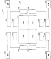
- FIG. 9 is a block diagram illustrating a configuration example of a display device that drives the display panel to be divided into a plurality of areas.
- the display device 100 includes a display panel 101, a plurality of driving substrates 102A, 102B, 102C, and 102D, and a plurality of power supplies 103A, 103B, 103C, and 103D.
- the display panel 101 includes one display screen 104, a plurality of source driver substrates 105A, 105B, 105C, and 105D, and a plurality of gate driver substrates 106A, 106B, 106C, and 106D.
- the display screen 104 is composed of four divided areas 104A, 104B, 104C, and 104D.
- the source driver boards 105A, 105B, 105C, and 105D and the gate driver boards 106A, 106B, 106C, and 106D are connected to the areas 104A, 104B, 104C, and 104D in the vertical and horizontal directions, respectively. .
- the source driver substrate 105A and the gate driver substrate 106A are connected to the area 104A.
- a source driver substrate 105B and a gate driver substrate 106B are connected to the area 104B.
- a source driver substrate 105C and a gate driver substrate 106C are connected to the area 104C.
- a source driver substrate 105D and a gate driver substrate 106D are connected to the area 104D.
- the driving substrate 102A is connected to the source driver substrate 105A, the gate driver substrate 106A, and the power source 103A.
- the driving substrate 102B is connected to the source driver substrate 105B, the gate driver substrate 106B, and the power source 103B.
- the driving substrate 102C is connected to the source driver substrate 105C, the gate driver substrate 106C, and the power source 103C.
- the driving substrate 102D is connected to the source driver substrate 105D, the gate driver substrate 106D, and the power source 103D.
- the driving substrates 102A, 102B, 102C, and 102D receive power supply voltages from the power sources 103A, 103B, 103C, and 103D, respectively.
- the driving substrates 102A, 102B, 102C, and 102D are connected to the source driver substrate 105A, the gate driver substrate 106A, the source driver substrate 105B, the gate driver substrate 106B, the source driver substrate 105C, and the gate driver substrate 106C, respectively.
- Image data, gradation voltage data, counter voltage (VCOM), CS voltage, gate voltage, LCD drive for each of the areas 104A, 104B, 104C, and 104D with respect to the source driver board 105D and the gate driver board 106D Provides information such as timing data.
- each source driver board 105A / gate driver board 106A, source driver board 105B / gate driver board 106B, source driver board 105C / gate driver board 106C, source driver board 105D / gate driver board 106D are divided into area 104A, The area 104B, the area 104C, and the area 104D are driven.
- Information output from each of the driving substrates 102A, 102B, 102C, and 102D connected to the power supplies 103A, 103B, 103C, and 103D is basically classified into the following three groups (P, Q, and R). can do.
- P Area-specific information video data
- gradation voltage data Data that needs to be coordinated between areas 104A, 104B, 104C, and 104D LCD drive timing data
- R Same among areas 104A, 104B, 104C, and 104D VCOM voltage, CS voltage, gate voltage
- the timing data classified into the Q group is used for synchronization among the drive circuits 102A, 102B, 102C, and 102D from the time when it is necessary to divide and transmit the signal as the display capacity increases. It is conventionally known that it is necessary to provide this mechanism, and various devices have been devised for synchronization.
- the VCOM voltage and the CS voltage must be essentially the same among the areas 104A, 104B, 104C, and 104D.
- Solution (i) is a method of securing a line for connecting a power source between substrates connected to each of the areas 104A, 104B, 104C, and 104D.
- Solution (ii) is to divide the drive timing and video processing by each area, but use only one circuit for the power supply and supply the voltage to each substrate.
- the signal system of the 60-inch class 4K2K (3840 ⁇ 2160) LCD is divided into four FHD systems, but there is one that has only one power system.
- the power supply in order to efficiently design and manufacture the power supply system by utilizing the conventional design technology, the power supply also needs to be divided into at least two, preferably four, according to the circuit meter.
- the present invention has been made in view of the above problems, and an object of the present invention is to prevent an overcurrent from flowing between the plurality of driver boards because the operation of the plurality of power supply circuits becomes an anxiety point. It is.
- a display device of the present invention includes first and second power supply circuits, a first power supply line connected to the first power supply circuit, and the second power supply circuit.
- a second power line connected to the display panel; and first and second driver boards for driving the display panel, wherein the first power line is connected to the first driver board.
- the power supply line is connected to the second driver board, and the first and second power supply lines are connected via a current limiting circuit that controls the outflow of overcurrent.
- the size of one of the first and second power supply circuits is reduced. This can simplify the power circuit design.
- first and second power supply lines are connected via a current limiting circuit that controls the outflow of overcurrent, even if a potential difference occurs between the first and second power supply lines, The potential difference can be smoothed and the display quality of the image can be prevented from deteriorating.
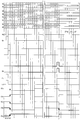
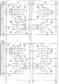
- FIG. 13 is a circuit diagram showing a distribution of pixel polarities (portion of FIG. 2) by the driving method of FIG.
- FIG. 13 is a circuit diagram showing a distribution of pixel polarities (portion of FIG. 3) by the driving method of FIG.
- FIG. 13 is a circuit diagram showing a distribution of light and dark regions (portion of FIG. 2) by the driving method of FIG.
- FIG. 13 is a circuit diagram showing a distribution of bright and dark regions (portion of FIG. 3) by the driving method of FIG. 12 is a timing chart illustrating another driving method of the liquid crystal panel of FIGS.
- FIG. 1 is a diagram illustrating a configuration of a liquid crystal display device 1 according to an embodiment of the present invention.
- the liquid crystal display device (display device) 1 corresponds to a video standard having a resolution (8K4K) that is 16 times the full HD resolution (for example, Super Hi-Vision having a resolution of horizontal 7680 pixels ⁇ vertical 4320 pixels). To do.
- the liquid crystal display device 1 includes a liquid crystal panel LCP, four drive substrates (timing controller substrates) CA, CB, CC, and CD, and four common electrode drive substrates COMA, COMB, COMC, and COMD.
- the liquid crystal display device 1 also includes an illumination device (not shown) for illuminating the liquid crystal panel LCP, an input processing circuit (not shown), and a pixel mapping circuit (not shown).
- the drive substrate CA includes a power supply circuit PA and a TCON (timing control) unit TA.
- the drive substrate CB includes a power supply circuit PB and a TCON unit TB.
- the drive substrate CC includes a power supply circuit PC and a TCON unit TC.
- the drive substrate CD includes a power supply circuit PD and a TCON unit TD.
- Each of the driving substrates CA, CB, CC, and CD includes two video processing circuits (not shown).
- Each of the TCON units TA, TB, TC, and TD includes two timing control units.
- the common electrode drive substrates COMA, COMB, COMC, and COMD each include a current limiting circuit 10 that is an overcurrent outflow prevention circuit.
- the liquid crystal panel LCP includes an active substrate 2 and a counter substrate 3 disposed so as to oppose the active substrate 2 via a liquid crystal (not shown).
- the liquid crystal panel LCP includes a display area D, four G (gate) driver substrates (first to fourth driver substrates) GA, GB, GC, GD, and four Cs (auxiliary capacitors) driver substrates (first capacitors). 1 to 4 driver boards) CsA, CsB, CsC, and CsD, and four S (source) driver boards (first to fourth driver boards) SA, SB, SC, and SD.
- Each of the G driver boards GA, GB, GC, GD, Cs driver boards CsA, CsB, CsC, CsD, and S driver boards SA, SB, SC, SD includes a current limiting circuit 10.
- the display area D is an image display area in which a plurality of pixels are arranged in a matrix.
- the display area D is a high-definition and large-screen image display area capable of displaying a 4K8K image.
- the display area D is not composed of a plurality of liquid crystal panels, but is composed of one liquid crystal panel LCP. As a result, it is possible to prevent variation in characteristics among the display panels, and it is possible to prevent display quality deterioration of the image.
- the display area D is composed of a plurality of display areas that are individually driven and controlled.
- the display area D is composed of four display areas (first to fourth divided areas) DA, DB, DC, and DD that are individually divided and driven.
- the upper left of the page is the display area DA
- the upper right is the display area DB
- the lower right is the display area DC
- the lower left is the display area DD.
- the display area D is described as being composed of the display areas DA to DD divided into a total of four parts, which is divided into two parts in the vertical direction and two parts in the horizontal direction.
- the display area may be divided into two in the vertical direction. Thereby, one image can be displayed by a plurality of display areas.
- the video signal is input to the input processing circuit from the outside.
- the video signal input to the input processing circuit may be a video signal (for example, Super Hi-Vision) having an 8K4K resolution in a block scan format or a video signal having an 8K4K resolution in a multi-display format. Of course, it may be a video signal having 4K2K resolution or a video signal having 2K1K resolution (full HD resolution).
- the block scan format is a method in which one frame (entire image having 8K4K resolution) is divided into 16 coarse (full HD resolution) whole images (so-called thinned images) and transmitted.
- each of the 16 video signals input to the input processing circuit is a rough overall image (full HD resolution).
- the multi-display format is a system in which one frame (entire image having 8K4K resolution) is divided into 16 without changing the fineness of the frame, and divided into 16 partial images for transmission.
- each of the 16 video signals input to the input processing circuit is a fine partial image (full HD resolution).
- the input processing circuit performs video data synchronization processing, ⁇ correction processing, color temperature correction processing, color gamut conversion processing, and the like, and outputs a video signal to the pixel mapping circuit.
- the pixel mapping circuit divides a video signal (resolution 2K2K) corresponding to the left half of the display area DA into two (full HD resolution video signal) and outputs the divided video signal to the video processing circuit of the drive substrate CA.
- the video signal corresponding to the right half of the video signal (resolution 2K2K) is divided into two (full HD resolution video signal) and output to the video processing circuit of the drive board, and the video signal corresponding to the left half of the display area DB ( (Resolution 2K2K) is divided into two (full HD resolution video signals) and output to the video processing circuit of the drive substrate CB, and two video signals (resolution 2K2K) corresponding to the right half of the display area DB (
- the video signal is divided into full HD resolution video signals and output to the video processing circuit of the drive substrate CB, and two video signals (resolution 2K2K) corresponding to the left half of the display area DC (full HD resolution video signals).
- the video signal corresponding to the right half of the display area DC (resolution 2K2K) is divided into two (full HD resolution video signal) and divided into two.
- the video signal output to the video processing circuit the video signal corresponding to the left half of the display area DD (resolution 2K2K) is divided into two (full HD resolution video signal) and output to the video processing circuit of the drive substrate CD for display.
- the video signal (resolution 2K2K) corresponding to the right half of the area DD is divided into two (full HD resolution video signal) and output to the video processing circuit of the drive substrate CD.
- the pixel mapping circuit outputs a synchronization signal (vertical synchronization signal, horizontal synchronization signal, clock signal, data enable signal, polarity inversion signal, etc.) to the TCON section TA of the driving substrate CA, and the TCON section TA that receives this outputs the synchronization signal.
- the synchronization signal is output to the inter-substrate shared line (not shown) that connects the drive substrates CA, CB, CC, and CD.
- the drive board CA, the common electrode drive board COMA / G driver board GA, the Cs driver board CsA, and the S driver board SA are driver boards for driving the display area DA.
- the Cs driver board CsB and S driver board SB are driver boards for driving the display area DB
- the drive board CC, common electrode drive board COMC, G driver board GC, Cs driver board CsC, and S driver board SC are display area DC.
- the driver board for driving, and the driving board CD, the common electrode driving board COMD, the G driver board GD, the Cs driver board CsD, and the S driver board SD are driver boards for driving the display area DD.
- the liquid crystal display device 1 includes each driver substrate connected to each of the four display areas DA to DD. As a result, each of the display areas DA to DD can be individually driven and controlled.
- the power supply circuits (first to fourth power supply circuits) PA, PB, PC, and PD are mounted on the drive substrates (first to fourth display control substrates) CA, CB, CC, and CD, respectively.
- Each of the power supply circuits PA, PB, PC, and PD is individually connected to a commercial power supply, and an input power supply voltage V0 is input from the connected commercial power supply.
- the power supply circuits PA, PB, PC, and PD generate voltages necessary for the operation of each circuit in the liquid crystal display device 1 from the input power supply voltage V0, and supply the voltages to the respective circuits.
- the power supply circuits PA, PB, PC, and PD are respectively driven by a common electrode driving substrate (first to fourth driver substrates) VCOM for driving COMA, COMB, COMC, and COMD, and a G driver substrate GA, GB, GC.
- a voltage Vg for driving GD, a voltage Vcs for driving CsA / CsB / CsC / CsD, and a voltage Vcc for driving S / SB / SC / SD are generated.
- the power supply circuits PA, PB, PC, and PD output the voltage Vcom to the power supply lines VcomL of the common electrode drive substrates COMA, COMB, COMC, and COMD, respectively.
- the power supply circuits PA, PB, PC, and PD output the voltage Vg to the power supply lines VgL of the G driver boards GA, GB, GC, and GD, respectively.
- the power supply circuits PA, PB, PC, and PD output the voltage Vcs to the power supply lines VcsL of the Cs driver substrates CsA, CsB, CsC, and CsD, respectively.
- the power supply circuits PA, PB, PC, and PD output the voltage Vcc to the power supply lines VccL of the S driver substrates SA, SB, SC, and SD, respectively.
- the power supply circuits PA, PB, PC, and PD supply power supply voltages to any one of the driver boards connected to the display areas DA to DD. That is, the power supply circuit PA is connected to a driver board connected to the display area DA, and supplies a power supply voltage to the driver board.
- the power supply circuit PB is connected to a driver board connected to the display area DB, and supplies a power supply voltage to the driver board.
- the power supply circuit PC is connected to a driver board connected to the display area DC, and supplies a power supply voltage to the driver board.
- the power supply circuit PD is connected to a driver board connected to the display area DD, and supplies a power supply voltage to the driver board.
- the number of power supply circuits is not necessarily four, and two power supply circuits (for example, the display area DA) that supply power supply voltages to two driver boards among the driver boards for driving the display areas DA to DD, respectively.
- a power supply circuit for supplying a power supply voltage to DB and a power supply circuit for supplying a power supply voltage to the display area DC / DD may be included.
- the power supply circuit can be reduced in size, and the design of the power supply circuit can be facilitated.
- the TCON unit TA receives a synchronization signal received from a pixel mapping circuit (not shown), cooperates with a video processing circuit (not shown), and performs video conversion such as gradation conversion processing and frame rate conversion (FRC) processing on the video signal.
- the S drive signal SCS is output to the S driver substrate SA
- the G drive signal GCS is output to the G driver substrate GA
- the Cs drive signal CsCS is output to the Cs driver substrate CsA.
- the TCON unit TB receives a synchronization signal received from a pixel mapping circuit (not shown), cooperates with a video processing circuit (not shown), and performs video conversion such as gradation conversion processing and frame rate conversion (FRC) processing on the video signal.
- the S drive signal SCS is output to the S driver substrate SB
- the G drive signal GCS is output to the G driver substrate GB
- the Cs drive signal CsCS is output to the Cs driver substrate CsB.
- the TCON unit TC receives a synchronization signal received from a pixel mapping circuit (not shown), cooperates with a video processing circuit (not shown), and performs video conversion such as gradation conversion processing and frame rate conversion (FRC) processing on the video signal.
- the S drive signal SCS is output to the S driver substrate SC
- the G drive signal GCS is output to the G driver substrate GC
- the Cs drive signal CsCS is output to the Cs driver substrate CsC.
- the TCON unit TD receives a synchronization signal received from a pixel mapping circuit (not shown) and cooperates with a video processing circuit (not shown) to convert the video signal into a video such as a gradation conversion process and a frame rate conversion (FRC) process.
- a video processing circuit not shown
- the S drive signal SCS is output to the S driver substrate SD
- the G drive signal GCS is output to the G driver substrate GD
- the Cs drive signal CsCS is output to the Cs driver substrate CsD.
- the S drive signal SCS includes a data signal, a data enable signal (DE signal), a source start pulse, and a source clock
- the G drive signal GCS includes an initial signal, a gate start pulse, and a gate clock.
- the gradation conversion processing corresponds to a combination of high-speed display processing (QS processing), panel vertical division driving (described in detail below), and 1 V inversion driving of data signal lines (described in detail below).
- QS processing high-speed display processing
- panel vertical division driving panel vertical division driving
- 1 V inversion driving of data signal lines described in detail below.
- the tone correction processing according to the pixel position may be included.
- each video processing circuit obtains a motion vector using any one of 16 video signals (full HD resolution, rough overall image), and supports the corresponding video signal.
- a partial image (full HD resolution) for interpolation may be generated using one of them (full HD resolution, fine partial image).
- the DE signal (for 1920 lines) extends one clock (for one line) and reaches 1921 lines. Therefore, when the width of the DE signal is monitored and it becomes 1921 lines, it is possible to perform error correction processing for starting up the DE signal with a delay of one clock.
- 12-bit transfer HDMI high definition multimedia interface, registered trademark
- the drive substrates CA, CB, CC, and CD synchronize their operations by exchanging or sharing various signals between the substrates.
- the drive board CA as a master sends an RDY (ready) signal to the slave drive board CB, and the drive board CB that receives the signal sends the RDY signal to the slave drive board as soon as the preparation is completed.
- the drive board CC that receives the signal and sends it to the CC sends the RDY signal to the slave drive board CD as soon as the preparation is completed, and the drive board CD that receives this sends the RDY signal to the drive board as soon as the preparation is completed.
- the drive substrate CA transmits an operation start (SRST) signal to the drive substrates CA to CD via the inter-substrate shared line (illustrated).
- the TCON unit TA of the drive substrates CA to CD receives the synchronization signal received from the pixel mapping circuit via the inter-substrate shared line. To the included TCON sections TA to TD).
- the fail-safe signal transmitted from the driving board in which the abnormality has occurred is received by all other driving boards. All the drive boards are instantaneously in a self-running state (black display) mode. Thereby, the video failure is avoided.
- each driver board (G driver board GA to GD, Cs driver board CsA to CsD, S driver board SA to SD, common electrode drive substrates COMA to COMD) can be prevented from flowing.
- the active substrate 2 is formed on a single glass substrate with gate wirings Ga to Gd extending in the row direction (a direction along the long side of the panel), a plurality of source wirings Sa to Sd extending in the column direction, and extending in the row direction. Cs (auxiliary capacitor) wirings CSa to CSd to be performed and CS trunk wirings Ma to Mh extending in the column direction are provided. A region defined by a plurality of source lines Sa to Sd and a plurality of gate lines Ga to Gd is the pixel.
- a TFT element for driving liquid crystal and a pixel electrode for driving the pixel connected to the TFT element are formed in the pixel.
- the TFT element has a source terminal, a drain terminal, and a gate terminal, the source terminal is connected to the source wiring, the drain terminal is connected to the pixel electrode, and the gate terminal is connected to the gate wiring.
- the counter substrate 3 includes a glass substrate, a color filter, a common electrode facing the pixel electrode, and common electrode connection portions 4A, 4B, 4C, and 4D connected to the common electrode.
- the side of the counter substrate 3 opposite to the side where the active substrate 2 is disposed is the image display surface side for the user to visually recognize.
- the color filter is arranged on the side of the glass substrate facing the active substrate 2.
- the color filter includes, for example, a filter that transmits red light, green light, and blue light, and any one of the filters is arranged in each pixel.
- the common electrodes are connected to each other in the display areas DA, DB, DC, and DD, and the common voltage Vcom is applied to the pixels from the connected common electrode connection portions 4A, 4B, 4C, and 4D. A signal for outputting is input.
- the liquid crystal panel LCP is provided with two source lines corresponding to the upper half (upstream side of the panel) of one pixel column, and two lines corresponding to the lower half (downstream side of the panel) of this pixel column.
- a so-called upper / lower divided double source structure (a structure in which four source wirings are provided per pixel column and four gate wirings can be selected at the same time) is provided.
- the writing time can be secured four times, and the structure is suitable for high-speed driving such as ultra-high definition display and quadruple speed driving.
- the liquid crystal panel LCP is a so-called multi-pixel system in which at least two pixel electrodes and two active elements are provided in one pixel, and viewing angle characteristics are improved by a bright region and a dark region formed in one pixel. It is possible to increase.
- the scanning signal lines Ga and Gb and the storage capacitor lines CSa and CSb are provided in the upper half (upstream side) of the panel, and the scanning signal lines are provided in the lower half (downstream side) of the panel.
- Gc and Gd and storage capacitor lines CSc and CSd are provided, and the upper half (upstream side) of one pixel column PL1 includes two pixels Pa and Pb adjacent in the column direction, and the lower half of the pixel column PL1 ( Two pixels Pc and Pd that are adjacent in the column direction are included on the downstream side, data signal lines Sa and Sb are provided corresponding to the upper half (upstream side) of the pixel column PL1, and the lower half of the pixel column PL1 Data signal lines Sc and Sd are provided corresponding to (downstream side).
- the TFT 12A connected to the pixel electrode 17A and the TFT 12a connected to the pixel electrode 17a are connected to the data signal line Sa and the scanning signal line Ga, respectively.
- 17A forms the storage capacitor line CSn and the storage capacitor CA
- the pixel electrode 17a forms the storage capacitor line CSa and the storage capacitor Ca
- the pixel electrode 17B out of the two pixel electrodes 17B and 17b included in the pixel Pb.
- the TFT 12B to be connected and the TFT 12b to be connected to the pixel electrode 17b are connected to the data signal line Sb and the scanning signal line Gb, the pixel electrode 17B forms the storage capacitor line CSa and the storage capacitor CB, and the pixel electrode 17b has the storage capacitor.
- a wiring CSb and a storage capacitor Cb are formed, and two pixel electrodes included in the pixel Pc are further formed.
- 7C and 17c, the TFT 12C connected to the pixel electrode 17C and the TFT 12c connected to the pixel electrode 17c are respectively connected to the data signal line Sc and the scanning signal line Gc, and the pixel electrode 17C includes the storage capacitor line CSm and the storage capacitor CC.
- the pixel electrode 17c forms the storage capacitor line CSc and the storage capacitor Cc, and the TFT 12D connected to the pixel electrode 17D and the TFT 12d connected to the pixel electrode 17d out of the two pixel electrodes 17D and 17d included in the pixel Pd.
- Each is connected to the data signal line Sd and the scanning signal line Gd, the pixel electrode 17D forms a storage capacitor line CSc and a storage capacitor CD, and the pixel electrode 17d forms a storage capacitor line CSd and a storage capacitor Cd.
- Four scanning signal lines Ga to Gd are simultaneously selected.
- the data signal lines Sa and Sc are arranged in the column direction at the left end, and the data signal lines Sb and Sd are arranged in the column direction at the right end, and the pixel column PL2 adjacent to the pixel column PL1.
- the data signal lines SA and SC are arranged at the left end in the column direction, and the data signal lines SB and SD are arranged at the right end in the column direction.
- the two pixel electrodes included in the pixel adjacent to the pixel electrode Pa are connected to the data signal line SB via separate TFTs, and the two pixels included in the pixel adjacent to the pixel electrode Pb.
- the electrodes are connected to the data signal line SA via separate TFTs, and the two pixel electrodes included in the pixel adjacent to the pixel electrode Pc are connected to the data signal line SD via separate TFTs, and the pixel electrode Pd And two pixel electrodes included in adjacent pixels are connected to the data signal line SC via separate TFTs.
- the configuration in the vicinity of the boundary between the upper half (first region) and the lower half (second region) is as shown in FIG. That is, of the two pixel electrodes 17X and 17x included in the pixel Px located at the bottom of the first region, the TFT 12X connected to the pixel electrode 17X and the TFT 12x connected to the pixel electrode 17x are respectively connected to the data signal line Sb and the scanning signal line.
- the pixel electrode 17X forms a storage capacitor with a storage capacitor line CSi
- the pixel electrode 17x forms a storage capacitor line with a storage capacitor line CSm
- the pixel Pc is located at the top of the second region. Yes.
- the CS trunk line Ma (first trunk line) and the CS trunk line Mb are provided close to one of the two short sides of the upper half of the active matrix substrate, and are in different phases by the CS driver CD1. Driven.
- the CS trunk wiring Mc (third trunk wiring) and the CS trunk wiring Md are provided close to the other of the two short sides of the upper half of the active matrix substrate so that the CS driver CD2 has different phases. Driven by.
- the CS trunk wiring Me / CS trunk wiring Mf (second trunk wiring) is provided in proximity to one of the two short sides of the lower half of the active matrix substrate, and each has a different phase by the CS driver CD3. Driven.
- the CS trunk wiring Mg / CS trunk wiring Mh (fourth trunk wiring) is provided close to the other of the two short sides of the lower half of the active matrix substrate, and the CS driver CD4 is in a different phase. Driven by.
- One storage capacitor line is connected to two CS trunk lines arranged on both sides thereof, and a modulation (pulse) signal having the same phase is transmitted from the two CS trunk lines to the one storage capacitor line. Is supplied.
- the storage capacitor line CSa is connected to the CS trunk lines Ma and Mc
- the storage capacitor line CSb is connected to the CS trunk lines Mb and Md
- the storage capacitor line CSc is connected to the CS trunk lines Me and Mg
- the storage capacitor line CSd is connected to CS trunk lines Mf and Mh. Therefore, for example, when the potentials of the CS trunk lines Ma and Mb are controlled to be in opposite phases, the potentials of the storage capacitor lines CSa and CSb are also reversed in phase, and in the pixel Pb, the pixel electrode of the two pixel electrodes 17B and 17b.
- the polarity of the data signal supplied to one data signal line is inverted every one vertical scanning period (1V), and two data signal lines provided corresponding to one pixel column in the same vertical scanning period.
- the polarity of the data signal supplied to one and the other is opposite.
- each data signal line is inverted by 1V (that is, the polarity inversion period is lengthened and power consumption is reduced), and the polarity distribution of the pixels in the screen is inverted by dots (thus turning off the TFT). Flicker caused by the pull-in voltage generated at the same time can be suppressed).
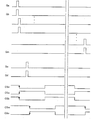
- the driving method of the part shown in FIGS. 10 and 11 of the liquid crystal panel is shown in the timing chart of FIG. As shown in FIG. 12, a positive data signal potential is supplied to the data signal lines Sa, SA, Sc, and SC during one vertical scanning period, and the data signal lines Sb, SB, Sd, and SD are During one vertical scanning period, a negative data signal potential is supplied.
- Simultaneous scanning of the scanning signal lines Ga and Gb starts at time t0, and simultaneous scanning of the scanning signal lines Ga to Gd ends at time t1 1H (vertical scanning period) after t0.
- a positive data signal potential is written to the pixel electrodes 17A and 17a
- a positive data signal potential is written to the pixel electrodes 17C and 17c
- a negative data signal potential is written to the pixel electrodes 17B and 17b.
- a negative data signal potential is written to the pixel electrodes 17D and 17d.
- the potential of the storage capacitor line CSn is shifted to the L (Low) side by the modulation signal sent from the CS trunk line Mb.
- the effective potential until the scan is lower than the written data signal potential (+) (becomes a dark region).
- the potential of the storage capacitor line CSa is shifted to the H (High) side by the modulation signal sent from the CS drivers CD1 and CD2 via the CS trunk lines Ma and Mc, and accordingly, the pixel electrode 17a And the effective potential until the next scanning rises higher than the written data signal potential (+) (becomes a bright region).
- the potential of the pixel electrode 17B rises (because the potential of the storage capacitor line CSa shifts to the H side), and the effective potential until the next scan is higher than the written data signal potential ( ⁇ ). It rises (becomes a dark area).
- the potential of the storage capacitor line CSm is shifted to the L (Low) side by the modulation signal sent from the CS trunk line Md, and accordingly, the potential of the pixel electrode 17C falls down until the next scan. Is lower than the written data signal potential (+) (becomes a dark region).
- the potential of the storage capacitor line CSc is shifted to the H (High) side by a modulation signal sent from the CS drivers CD3 and CD4 via the CS trunk lines Me and Mg, and accordingly, the pixel electrode 17c And the effective potential until the next scanning rises higher than the written data signal potential (+) (becomes a bright region).
- the potential of the storage capacitor line CSb is shifted to the L side by the modulation signal sent from the CS drivers CD1 and CD2 via the CS trunk lines Mb and Md, and accordingly, the potential of the pixel electrode 17b is The effective potential until the next scan is lowered (becomes a bright region) than the written data signal potential ( ⁇ ).
- the bright area and the dark area of each pixel are continuously maintained.
- the CS trunk wiring is divided into the upper half (first region) and the lower half (second region), in the vicinity of the boundary between the upper half (first region) and the lower half (second region).
- the storage capacitor line CSm belonging to the second region can be modulated and driven without being restricted by the modulation timing of the CS signal in the first region.
- the display near the boundary between the first and second regions can be adjusted (corrected).
- the scanning signal line Gc is the (n + 2160) th line from the upper long side
- the scanning signal line Gd is the (n + 2161) th line.
- the scanning signal line Gc is a scanning signal provided in the upper half of the panel. If the data signal of the nth frame of the Nth frame is written to the line Ga, the scanning signal line Gc provided in the lower half of the panel has the (n + 2160) th line of the (N ⁇ 1) th frame as the previous frame. Data signal is written. By doing so, the feeling of display deviation at the top and bottom of the panel is suppressed.
- the scanning signal lines Ga and Gb positioned at the top (first and second) of the first region and the scanning signal lines Gc and Gd positioned at the top (first and second) of the second region are shown. Although it is scanning simultaneously, it is not limited to this. As shown in FIG. 17, the scanning signal lines Gc and Gd positioned at the top (first and second) of the second region are scanned while being delayed for a certain period from the scanning signal lines Ga and Gb positioned at the top of the first region. May be. At this time, in the case where the signal of each CS is modulated in conjunction with the vertical (gate) scanning, the modulation signal of the CS in the second region is also driven with a certain delay from that of the CS in the first region. It will be.
- nH n is a natural number
- the CS modulation signal near the boundary between the first and second areas is adjusted, and the display is adjusted. (Correction) is also possible.
- the polarity of the data signal supplied to one source line is inverted every vertical scanning period (1 V), and the data signal supplied to one and the other of two adjacent source lines in the same vertical scanning period.
- the polarity is reversed.
- each source wiring is inverted by 1V (that is, the polarity inversion period is lengthened and power consumption is reduced), and the polarity distribution of the pixels in the screen is inverted by dots (thus turning off the TFT). Flicker caused by a pull-in voltage sometimes generated can be suppressed).
- the G driver board GA / GB / GC / GD, the Cs driver board CsA / CsB / CsC / CsD, and the S driver board SA / SB / SC / SD are arranged on the active board 2. Yes.
- Each of the G driver substrates GA, GB, GC, and GD includes a power line VgL, a current limiting circuit 10, and a gate driver chip (not shown).
- the G driver substrate GA is provided along one of the two short sides of the upper half of the liquid crystal panel LCP, and includes a plurality of gate driver chips (not shown) arranged in the column direction.
- the G driver substrate GB is provided along the other of the two short sides of the upper half of the liquid crystal panel LCP, and includes a plurality of gate driver chips (not shown) arranged in the column direction.
- the G driver substrate GC includes a plurality of gate driver chips (not shown) provided along one of the two short sides of the lower half of the liquid crystal panel LCP and arranged in the column direction.
- the G driver substrate GD is provided along the other of the two short sides of the lower half of the liquid crystal panel LCP, and includes a plurality of gate driver chips (not shown) arranged in the column direction.
- Each gate wiring provided in the upper half of the panel is driven by a G driver substrate GA / GB
- each gate wiring provided in the lower half of the panel is a G driver. It is driven by the substrate GC / GD. That is, one gate wiring is connected to two G driver boards arranged on both sides thereof, and scanning signals (pulses) having the same phase are supplied from the two G driver boards to the one gate wiring. By so doing, it is possible to suppress variation in signal dullness (the degree of signal dullness varies depending on the position in the row direction) due to CR (time constant) of the gate wiring.
- the power supply line VgL arranged on each of the G driver boards GA, GB, GC, and GD is connected to the current limiting circuit 10 and a plurality of gate driver chips (not shown) arranged on each of them.
- the power supply line (first power supply line) VgL arranged on the G driver board GA and the power supply line (second power supply line) VgL arranged on the G driver board GD are arranged in parallel with each other. Connection is made via a current limiting circuit 10.
- the power supply line VgL arranged on the G driver board GA has a branched end on the side different from the input end to which the input voltage Vg from the power supply circuit PA is input.
- One end of the branch is connected to the input terminal VIN of the current limiting circuit 10 disposed on the G driver board GA, and the other end of the branch is the G driver board.
- the output terminal portion VOUT of the current limiting circuit 10 disposed in the GD is connected.
- the power supply line VgL arranged on the G driver board GD has a branched end on the side different from the input end to which the input voltage Vg from the power supply circuit PD is input.
- One branching end is connected to the input terminal VIN of the current limiting circuit 10 arranged on the G driver board GD, and the other branching end is connected to the G driver board GD.
- the output terminal portion VOUT of the current limiting circuit 10 disposed in the GA is connected.
- the power supply line VgL arranged on the G driver board (first power supply line) GB and the power supply line (first power supply line) VgL arranged on the G driver board GC are arranged in parallel to each other.
- the current limiting circuit 10 is connected.
- the power supply line VgL arranged on the G driver board GB has a branched end on the side different from the input end to which the input voltage Vg from the power supply circuit PB is input.
- One end of the branch is connected to the input terminal VIN of the current limiting circuit 10 disposed on the G driver board GB, and the other end of the branch is the G driver board.
- the output terminal portion VOUT of the current limiting circuit 10 arranged in the GC is connected.
- the power supply line VgL arranged on the G driver board GC has a branched end portion different from the input end portion to which the input voltage Vg from the power supply circuit PC is input.
- One end of the branch is connected to the input terminal VIN of the current limiting circuit 10 disposed on the G driver board GC, and the other end of the branch is the G driver board. It is connected to the output terminal portion VOUT of the current limiting circuit 10 arranged in GB.
- the power line VgL arranged on each of the G driver boards GA, GB, GC, GD is held at the voltage Vg by the input of the voltage Vg from each of the power circuits PA, PB, PC, PD. Yes.
- the G driver boards GA, GB, GC, and GD are assigned to the G driver boards GA, GB, GC, and GD, respectively.
- the gate driver chip (not shown) generates a scanning signal GS for turning on the TFT element connected to each gate wiring.
- the G driver boards GA, GB, GC, and GD scan the gate wirings arranged in the display areas DA, DB, DC, and DD, respectively, sequentially from the top of the screen to the bottom or from the bottom to the top. As a result, the generated scanning signal GS is output.
- the current limiting circuit 10 is a circuit for detecting an overcurrent input from the terminal portion VIN and preventing the detected overcurrent from being output from the output terminal portion VOUT.
- the current limiting circuit (first current limiting circuit) 10 disposed on the G driver board GA prevents an overcurrent from being output to the G driver board GD connected via the power supply line VgL.
- the current limiting circuit (second current limiting circuit) 10 disposed on the driver board GD prevents an overcurrent from being output to the G driver board GA connected via the power supply line VgL.
- the current limiting circuit 10 disposed in the G driver board (first current limiting circuit) GB prevents an overcurrent output to the G driver board GC connected via the power supply line VgL.
- the current limiting circuit (second current limiting circuit) 10 disposed on the driver board GC prevents output of an overcurrent to the G driver board GB connected via the power supply line VgL.
- the G driver substrate GA is connected to one end of the gate wirings Ga and Gb, and by outputting the scanning signal GS to the gate wirings Ga and Gb, a gate voltage is applied to the gate wirings Ga and Gb. It is a driver substrate for gate wiring to output.
- the G driver substrate GD is connected to one end of the gate wirings Gc and Gd, and outputs a scanning signal GS to the gate wirings Gc and Gd, thereby outputting a gate voltage to the gate wirings Gc and Gd. This is a driver board for use.
- the current limiting circuit 10 is arranged between the power supply lines VgL of the G driver boards GA and GD, it is possible to prevent inflow of overcurrent due to unstable operation of the power supply circuits PA and PB.
- the G driver substrate GB is connected to the other end of the gate wiring Ga ⁇ Gb, and outputs a gate voltage to the gate wiring Ga ⁇ Gb by outputting a scanning signal GS to the gate wiring Ga ⁇ Gb.
- the G driver substrate GC is connected to the other end of the gate lines Gc and Gd, and outputs a scanning voltage GS to the gate lines Gc and Gd, thereby outputting a gate voltage to the gate lines Gc and Gd.
- the power line VgL of the G driver board GB / GC is connected to each other, it is possible to prevent a potential difference from being generated between the power line VgL of the G driver board GB and the power line VgL of the G driver board GC. Further, damage to the gate wirings Ga, Gb, Gc, and Gd can be prevented.
- the current limiting circuit 10 is arranged between the power supply lines VgL of the G driver boards GB and GC, it is possible to prevent inflow of overcurrent due to unstable operation of the power supply circuits PB and PC.
- Each of the S driver substrates SA, SB, SC, and SD includes a power supply line VccL, a current limiting circuit 10, and a plurality of source driver chips (not shown).
- the S driver board SA and the S driver board SB are juxtaposed, and the S driver board SC and the S driver board SD are juxtaposed.
- the S driver substrate SA is provided along the left side (display area DA) of one long side of the upper half of the liquid crystal panel LCP, and the S driver substrate SB is formed of one long side of the upper half of the liquid crystal panel LCP.
- the S driver substrate SC is provided along the right side (display region DC) of one long side of the lower half of the liquid crystal panel LCP, and the S driver substrate SD is provided along the right side (display region DB).
- the lower half of the panel LCP is provided along the left side (display area DD) of one long side.
- Each source wiring provided in the display area DA is driven by the S driver substrate SA, and each source wiring provided in the display area DB is driven by the S driver substrate SB, and each source wiring provided in the display area DC.
- Each source wiring provided in the display area SC is driven by the S driver substrate SD.
- a relay line that connects the source wiring and the source terminal on the short side of the panel is provided on the counter substrate side, or other than the source layer of the active substrate (the source / drain electrode formation layer of the TFT), that is, gate insulation It can also be provided in a lower layer (gate layer) of the film or a layer between the source layer and the ITO layer (pixel electrode formation layer).
- the power supply line VccL arranged on each of the S driver substrates SA, SB, SC, and SD is connected to the current limiting circuit 10 and a plurality of source driver chips (not shown) arranged on each of them.
- the power supply line (first power supply line) VccL arranged on the S driver board SA and the power supply line (second power supply line) VccL arranged on the S driver board SB are arranged in parallel to each other. Connection is made via a current limiting circuit 10.
- the power supply line VccL arranged on the S driver substrate SA has a branched end on the side different from the input end to which the input voltage Vcc from the power supply circuit PA is input.
- One branching end is connected to the input terminal portion VIN of the current limiting circuit (first current control circuit) 10 arranged on the S driver substrate SA, and is branched.
- the other end is connected to the output terminal portion VOUT of the current limiting circuit (second current control circuit) 10 disposed on the S driver substrate SB.
- the power supply line VccL arranged on the S driver substrate SB is branched at an end different from the input end to which the input voltage Vcc from the power supply circuit PB is input.
- One end of the branch is connected to the input terminal VIN of the current limiting circuit 10 disposed on the S driver board SB, and the other end of the branch is the S driver board.
- the output terminal portion VOUT of the current limiting circuit 10 disposed in the SA is connected.
- the power supply line (first power supply line) VccL arranged on the S driver board SC and the power supply line (second power supply line) VccL arranged on the S driver board SD are arranged in parallel to each other.
- the current limiting circuit 10 is connected.
- the power supply line VccL arranged on the S driver substrate SC has a branched end on the side different from the input end to which the input voltage Vcc from the power supply circuit PC is input.
- One end of the branch is connected to the input terminal portion VIN of the current limiting circuit (first current control circuit) 10 arranged on the S driver substrate SC, and is branched.
- the other end is connected to the output terminal portion VOUT of the current limiting circuit 10 disposed on the S driver substrate SD.
- the power supply line VccL arranged on the S driver substrate SD is branched at an end portion different from the input end portion to which the input voltage Vcc from the power supply circuit PD is input.
- One branching end is connected to the input terminal portion VIN of the current limiting circuit (second current control circuit) 10 arranged on the S driver board SD, and is branched. The other end is connected to the output terminal portion VOUT of the current limiting circuit 10 disposed on the S driver substrate SC.
- the power supply line VccL arranged on each of the S driver boards SA, SB, SC, and SD is held at the voltage Vcc by inputting the voltage Vcc from each of the power supply circuits PA, PB, PC, and PD. Yes.
- S driver boards SA, SB, SC, and SD When the S drive signal SCS is input to the S driver boards SA, SB, SC, and SD from the TCON sections TA, TB, TC, and TD, the S driver boards SA, SB, SC, and SD are assigned to the S driver boards SA, SB, SC, and SD, respectively.
- a source driver chip (not shown) generates a source driving signal SS.
- each of the S driver substrates SA, SB, SC, and SD outputs the generated source drive signal SS to each source wiring.
- image data data signal
- the current limiting circuit 10 is a circuit for detecting an overcurrent input from the terminal portion VIN and preventing the detected overcurrent from being output from the output terminal portion VOUT.
- the current limiting circuit 10 disposed on the S driver board SA prevents overcurrent output to the S driver board SB connected via the power supply line VccL, and is disposed on the S driver board SB.
- the current limiting circuit 10 prevents an overcurrent output to the S driver substrate SA connected via the power supply line VccL.
- the current limiting circuit 10 disposed on the S driver substrate SC prevents an overcurrent output to the S driver substrate SD connected via the power supply line VccL, and is disposed on the S driver substrate SD.
- the current limiting circuit 10 prevents an overcurrent from being output to the S driver substrate SC connected via the power supply line VccL.
- the S driver substrates SA and SB are connected to the source lines Sa and Sb, respectively, and by outputting the source drive signal SS to the source lines Sa and Sb, a signal voltage is applied to the source lines Sa and Sb.
- This is a source wiring driver board to output.
- the source lines Sa and Sb can be prevented from being damaged.
- the current limiting circuit 10 is disposed between the power supply lines VgL of the S driver boards SA and SB, it is possible to prevent inflow of overcurrent due to unstable operation of the power supply circuits PA and PB.
- the S driver substrates SC and SD are connected to the source lines Sc and Sd, respectively, and output the signal voltage to the source lines Sc and Sd by outputting the source drive signal SS to the source lines Sc and Sd.
- This is a source wiring driver board.
- the power line VgL of the S driver board SC / SD is connected to each other, a potential difference is prevented from being generated between the power line VgL of the S driver board SC and the power line VgL of the S driver board SD.
- the source lines Sc and Sd can be prevented from being damaged.
- the current limiting circuit 10 is arranged between the power lines VgL of the S driver boards SC and SD, it is possible to prevent an inflow of overcurrent due to unstable operation of the power circuits PC and PD.
- Each of the Cs driver boards CsA, CsB, CsC, and CsD includes a power line VcsL and a current limiting circuit 10.
- CS trunk lines (not shown) are arranged along the outside of the display areas DA, DB, DC, and DD.
- the Cs driver boards CsA and CsD are arranged along the left side of the display area D, and the Cs driver boards CsB and CsC are arranged along the right side of the display area D.
- the Cs driver substrate CsA is connected to one end portion of the Cs wiring arranged across the display areas DA and DB via the Cs trunk wiring, and the Cs driver board CsB is connected to the display area DA via the Cs trunk wiring.
- -It is connected to the other end of the Cs wiring arranged across DB.
- the Cs driver substrate CsD is connected to one end of the Cs wiring arranged over the display area DD / DC via the Cs trunk wiring, and the Cs driver substrate CsC is displayed via the Cs trunk wiring. It is connected to the other end of the Cs wiring arranged over the regions DD and DC.
- the Cs driver substrate CsA drives the Cs trunk wiring to which one of the Cs wirings Csa is connected and the Cs trunk wiring to which one of the Cs wirings Csb is connected so as to be in different phases.
- the Cs driver substrate CsB drives the Cs trunk wiring to which the other Cs wiring Csa is connected and the Cs trunk wiring to which the other Cs wiring Csb is connected so as to be in different phases.
- the Cs driver substrate CsD drives the Cs trunk line to which one of the Cs lines Csc is connected and the Cs trunk line to which one of the Cs lines Csd is connected so as to be in different phases.
- the Cs driver substrate CsC drives the Cs trunk wiring to which the other Cs wiring Csc is connected and the Cs trunk wiring to which the other Cs wiring Csd is connected so as to be in different phases.
- one Cs wiring is connected to the Cs driver board through connection to two CS trunk wirings arranged on both sides thereof, and is identical to one Cs wiring through these two CS trunk wirings.
- a phase modulation (pulse) signal is provided.
- the pixel electrode 17B of the two pixel electrodes 17B and 17b forms a capacitance with the Cs wiring CSa, and the pixel electrode 17b has the Cs wiring CSb.
- the effective potential of the pixel electrode 17B is shifted in the direction approaching the center potential, while the effective potential of the pixel electrode 17b is formed. Can be shifted in a direction away from the center potential (by this, a dark region corresponding to the pixel electrode 17B and a bright region corresponding to the pixel electrode 17b are formed in one pixel).
- the power supply lines VcsL arranged on each of the Cs driver boards CsA, CsB, CsC, and CsD are connected to the current limiting circuits 10 arranged on each of them.
- the power supply line (first power supply line) VcsL arranged on the Cs driver substrate CsA and the power supply line (second power supply line) VcsL arranged on the Cs driver substrate CsD are arranged in parallel to each other. Connection is made via a current limiting circuit 10.
- the power supply line VcsL arranged on the Cs driver substrate CsA has a branched end on the side different from the input end to which the input voltage Vcs from the power supply circuit PA is input.
- One branched end is connected to the input terminal VIN of the current limiting circuit (first current control circuit) 10 arranged on the Cs driver substrate CsA, and is branched.
- the other end is connected to the output terminal portion VOUT of the current limiting circuit (second current control circuit) 10 arranged on the Cs driver substrate CsD.
- the power supply line (second power supply line) VcsL arranged on the Cs driver substrate CsD is branched at an end portion different from the input end portion to which the input voltage Vcs from the power supply circuit PD is input. .
- One branching end is connected to the input terminal VIN of the current limiting circuit (second current control circuit) 10 arranged on the Cs driver substrate CsD, and is branched. The other end is connected to the output terminal portion VOUT of the current limiting circuit 10 disposed on the Cs driver substrate CsA.
- the power supply line (first power supply line) VcsL arranged on the Cs driver board CsB and the power supply line (second power supply line) VcsL arranged on the Cs driver board CsC are arranged in parallel to each other.
- the current limiting circuit 10 is connected.
- the power supply line VcsL arranged on the Cs driver board CsB has a branched end on the side different from the input end to which the input voltage Vcs from the power supply circuit PB is input.
- One end of the branch is connected to the input terminal portion VIN of the current limiting circuit (first current control circuit) 10 arranged on the Cs driver substrate CsB, and is branched.
- the other end is connected to the output terminal portion VOUT of the current limiting circuit (second current control circuit) 10 disposed on the Cs driver substrate CsC.
- the power supply line VcsL arranged on the Cs driver board CsC has a branched end on the side different from the input end to which the input voltage Vcs from the power supply circuit PC is input.
- One end of the branch is connected to the input terminal VIN of the current limiting circuit 10 disposed on the Cs driver substrate CsC, and the other end branched is the Cs driver substrate. It is connected to the output terminal portion VOUT of the current limiting circuit 10 arranged in CsB.
- the power lines VcsL arranged on the Cs driver boards CsA, CsB, CsC, and CsD are respectively held at the voltage Vcs by inputting the voltages Vcs from the power circuits PA, PB, PC, and PD, respectively. Yes.
- each Cs wiring is transmitted from the Cs driver board CsA, CsB, CsC, and CsD.
- a Cs drive signal CsS for output to the is generated.
- the Cs driver substrates CsA, CsB, CsC, and CsD output Cs drive signals CsS to Cs wirings arranged in the display areas DA, DB, DC, and DD, respectively. As a result, the voltage applied to each pixel is held until the next image rewriting timing.
- the current limiting circuit 10 is a circuit for detecting an overcurrent input from the terminal portion VIN and preventing the detected overcurrent from being output from the output terminal portion VOUT.
- the current limiting circuit 10 disposed on the Cs driver substrate CsA prevents an overcurrent output to the Cs driver substrate CsD connected via the power supply line VcsL, and is disposed on the Cs driver substrate CsD.
- the current limiting circuit 10 prevents an overcurrent from being output to the Cs driver substrate CsA connected via the power supply line VcsL.
- the current limiting circuit 10 disposed on the Cs driver substrate CsB prevents an overcurrent output to the Cs driver substrate CsC connected via the power supply line VcsL, and is disposed on the Cs driver substrate CsC.
- the current limiting circuit 10 prevents an overcurrent from being output to the Cs driver board CsB connected via the power supply line VcsL.
- the Cs driver substrate CsA is connected to one end of the Cs wiring Csa / Csb, and the Cs driver substrate CsD is connected to one end of the Cs wiring Csc / Csd.
- This is a storage capacitor wiring driver board for outputting Cs voltage to Csb, Csc, and Csd.
- the Cs driver substrate CsB is connected to the other end of the Cs wiring Csa / Csb
- the Cs driver substrate CsC is connected to the other end of the Cs wiring Csc / Csd, so that the Cs wiring Csa / Csb is connected.
- a driver board for auxiliary capacitance wiring for causing Csc / Csd to output a Cs voltage.
- the current limiting circuit 10 is arranged between the power supply lines VcsL of the Cs driver boards CsA and CsD, it is possible to prevent an overcurrent from flowing due to unstable operation of the power supply circuits PA and PD.
- the current limiting circuit 10 is arranged between the power supply lines VcsL of the Cs driver boards CsB and CsC, it is possible to prevent inflow of overcurrent due to unstable operation of the power supply circuits PB and PC.
- the common electrode drive substrates COMA, COMB, COMC, and COMD each include a power line VcomL and a current limiting circuit 10.
- the common electrode drive substrate COMA and the common electrode drive substrate COMB are juxtaposed, and the common electrode drive substrate COMA is connected to the common electrode connection portion 4A connected to the common electrode.
- the common electrode connection portion 4B connected to the common electrode is connected.
- the common electrode drive substrate COMC and the common electrode drive substrate COMD are juxtaposed, the common electrode drive substrate COMC is connected to the common electrode connection portion 4C connected to the common electrode, and the common electrode drive substrate COMD is The common electrode connection portion 4D connected to the common electrode is connected.
- the power supply lines VcomL arranged on each of the common electrode drive substrates COMA, COMB, COMC, and COMD are connected to the current limiting circuits 10 arranged on each of them.
- the power supply line (first power supply line) VcomL arranged on the common electrode drive substrate COMA and the power supply line (second power supply line) VcomL arranged on the common electrode drive substrate COMB are arranged in parallel with each other. Connected through a current limiting circuit 10.
- the power supply line VcomL arranged on the common electrode drive substrate COMA has a branched end on the side different from the input end to which the input voltage Vcom from the power supply circuit PA is input.
- One of the branched ends is connected to the input terminal portion VIN of the current limiting circuit (first current limiting circuit) 10 disposed on the common electrode driving substrate COMA.
- the other end is connected to the output terminal portion VOUT of the current limiting circuit (second current limiting circuit) 10 disposed on the common electrode drive substrate COMB.
- the power supply line VcomL arranged on the common electrode drive board COMB has a branched end on the side different from the input end to which the input voltage Vcom from the power supply circuit PB is input.
- One branching end is connected to the input terminal VIN of the current limiting circuit 10 arranged on the common electrode drive substrate COMB, and the other branching end is connected to the common electrode.
- the output terminal portion VOUT of the current limiting circuit 10 disposed on the drive substrate COMA is connected.
- the power supply line (first power supply line) VcomL disposed on the common electrode drive substrate COMC and the power supply line (second power supply line) VcomL disposed on the common electrode drive substrate COMD are parallel to each other. Are connected via a current limiting circuit 10.
- the power supply line VcomL arranged on the common electrode drive substrate COMC has a branched end on the side different from the input end where the input voltage Vcom from the power supply circuit PC is input.
- One end of the branch is connected to the input terminal VIN of the current limit circuit 10 (first current limit circuit) disposed on the common electrode drive substrate COMC.
- the other end is connected to the output terminal portion VOUT of the current limiting circuit (second current limiting circuit) 10 disposed on the common electrode drive substrate COMD.
- the power supply line VcomL arranged on the common electrode drive substrate COMD branches off at an end portion different from the input end portion to which the input voltage Vcom from the power supply circuit PD is input.
- One branching end is connected to the input terminal VIN of the current limiting circuit 10 disposed on the common electrode drive substrate COMD, and the other branching end is connected to the common electrode.
- the output terminal portion VOUT of the current limiting circuit 10 disposed on the driving substrate COMC is connected.
- the power lines VcomL arranged on the common electrode drive substrates COMA, COMB, COMC, and COMD are respectively held at the voltages Vcom by inputting the voltages Vcom from the power circuits PA, PB, PC, and PD, respectively. ing.
- the common electrode drive substrates COMA, COMB, COMC, and COMD When the voltage Vcom is input to the common electrode drive substrates COMA, COMB, COMC, and COMD from the TCON sections TA, TB, TC, and TD, the common electrode drive substrates COMA, COMB, COMC, and COMD are output to the common electrodes.
- a common electrode signal COMS indicating the voltage Vcom to be generated is generated.
- Each of the common electrode drive substrates COMA, COMB, COMC, and COMD outputs the generated common electrode signal COMS to each of the common electrode connection portions 4A, 4B, 4C, and 4D.
- the common voltage Vcom is applied to each of the common electrodes in each of the display areas DA, DB, DC, and DD.
- the current limiting circuit 10 is a circuit for detecting an overcurrent input from the terminal portion VIN and preventing the detected overcurrent from being output from the output terminal portion VOUT.
- the current limiting circuit 10 disposed on the common electrode drive substrate COMA prevents output of overcurrent to the common electrode drive substrate COMB connected via the power line VcomL, and is disposed on the common electrode drive substrate COMB.
- the current limiting circuit 10 prevents an overcurrent from being output to the common electrode drive substrate COMA connected via the power line VcomL.
- the current limiting circuit 10 disposed on the common electrode drive substrate COMC prevents an overcurrent from being output to the common electrode drive substrate COMD connected via the power line VcomL, and is disposed on the common electrode drive substrate COMD.
- the current limiting circuit 10 prevents the output of overcurrent to the common electrode drive substrate COMC connected via the power supply line VcomL.
- each of the common electrode drive substrates COMA and COMB is connected to the common electrode connection portions 4A and 4B connected to the common electrode, and the common electrode driver that outputs the common voltage to the common electrode. It is a substrate.
- each of the common electrode drive substrates COMC and COMD is connected to each of the common electrode connection portions 4C and 4D connected to the common electrode, and is a common electrode driver substrate that outputs the common voltage to the common electrode. is there.
- the current limiting circuit 10 is arranged between the power supply lines VcomL of the common electrode connecting portions 4A and 4B, it is possible to prevent an inflow of overcurrent due to unstable operation of the power supply circuits PA and PB.
- the current limiting circuit 10 is arranged between the power supply lines VcomL of the common electrode connecting portions 4C and 4D, it is possible to prevent an inflow of overcurrent due to unstable operation of the power supply circuit PC / PD.
- the liquid crystal display device 1 may include a backlight (not shown).
- the backlight controller receives the video signal output from the pixel mapping circuit, outputs a backlight control signal to the backlight driver, and the backlight is driven by the backlight driver.
- the backlight is divided into a plurality of parts, and the brightness of each backlight is individually adjusted according to the video signal (active backlight).
- a power supply controller (not shown) monitors the supply power level of the commercial power supply connected to each of the four power supply circuits PA, PB, PC, and PD. For some reason, one or more commercial power supplies are abnormal (supplied) When the power level decreases), 1 power line to the backlight (for example, 3 systems for R, B, and G) and 1 power line to the drive boards CA to CD (for example, 1 system) While switching to one or more normal commercial power sources, an abnormality occurrence signal is output to the backlight controller. Upon receiving this abnormality occurrence signal, the backlight controller outputs a control signal that lowers the upper limit of the luminance of the backlight to the backlight driver. As a result, it is possible to avoid damage to the drive substrates CA to CD due to an unexpected abnormality of the commercial power supply.
- the power supply controller 1 When the power supply controller is not required to have four power supply circuits and only one power supply circuit connected to a commercial power supply can be provided, the power supply controller 1 The power supply level of one commercial power supply is monitored, and if for some reason an abnormality occurs in this commercial power supply (decrease in the power supply level), an abnormality occurrence signal is output to the backlight controller. Further, the backlight controller can output a control signal that lowers the upper limit of the luminance of the backlight to the backlight driver).
- the liquid crystal display device 1 includes one liquid crystal panel LCP that is not divided into a plurality of parts.
- the liquid crystal panel LCP has a display area D for image display that has a high definition and a large screen.
- the display area D is a high-definition display area capable of displaying 4K8K images.
- the liquid crystal display device 1 controls the display area D individually for each of the four divided areas of the display areas DA, DB, DC, and DD. One image is displayed on the whole of D.
- the display areas DA, DB, DC, and DD are display areas that are individually driven and controlled, and the liquid crystal display device 1 is for driving each of the display areas DA, DB, DC, and DD.
- the driver boards connected to the display areas DA, DB, DC, and DD are provided.
- the liquid crystal display device 1 includes a drive substrate CA, a common electrode drive substrate COMA, a G driver substrate GA, a Cs driver substrate CsA, an S driver substrate SA, which are driver substrates for driving control of the display area DA, and a display area DB.
- Driving board CB which is a driver board for driving control, common electrode driving board COMB, G driver board GB, Cs driver board CsB, S driver board SB, and driving board CC which is a driver board for driving control of the display area DC Common electrode drive board COMMC / G driver board GC / Cs driver board CsC / S driver board SC and drive board CD / common electrode drive board COMD / G driver board GD / Cs which are driver boards for driving control of the display area DD And a driver board CsD / S driver board SD.
- the display area D is composed of the display areas DA to DD that are driven and controlled by each of the plurality of driver boards, a high-resolution image can be displayed at high speed.
- the liquid crystal display device 1 includes a plurality of power supply circuits PA, PB, PC, and PD for supplying a power supply voltage to each of the driver substrates for driving the display areas DA, DB, DC, and DD. .
- each of the divided display areas DA, DB, DC, DD is connected to each other, and a plurality of power supply circuits PA, PB, PC, PD is provided.
- the liquid crystal display device 1 includes a power supply circuit PA for supplying a power supply voltage to the drive substrate CA, the common electrode drive substrate COMA, the G driver substrate GA, the Cs driver substrate CsA, and the S driver substrate SA, and the drive of the display region DB.
- a power supply circuit PA for supplying a power supply voltage to the drive substrate CA, the common electrode drive substrate COMA, the G driver substrate GA, the Cs driver substrate CsA, and the S driver substrate SA, and the drive of the display region DB.
- Power supply circuit PB for supplying power supply voltage to control drive substrate CB, common electrode drive substrate COMB, G driver substrate GB, Cs driver substrate CsB, S driver substrate SB, drive substrate CC, common electrode drive substrate COMC, Power supply circuit PC for supplying power supply voltage to G driver board GC / Cs driver board CsC / S driver board SC and drive board CD / common electrode drive board COMD / G driver board GD / Cs driver board CsD / S driver board And a power supply circuit PD for supplying a power supply voltage to the SD.
- the liquid crystal display device 1 a driver for driving connected to each of the display areas DA, DB, DC, and DD, instead of supplying a power supply voltage to each driver board from one large power supply circuit.
- a plurality of power supply circuits PA, PB, PC, and PD for supplying a power supply voltage to each of the substrates are provided.
- the liquid crystal display device 1 includes corresponding power supply circuits PA, PB, PC, and PD for each display area DA, DB, DC, and DD.
- each of the power supply circuits PA, PB, PC, and PD is mounted on each of the drive substrates CA, CB, CC, and CD. can do.
- the liquid crystal display device 1 since the sizes of the plurality of power supply circuits PA, PB, PC, and PD can be kept small, even if the display area D is high definition such as 4K8K, for example, relative to 4K2K or the like. In particular, it is possible to use a design method for a power supply circuit having a size used for a display region having a small capacity. For this reason, the liquid crystal display device 1 has an advantage that the power supply circuit can be easily designed and simplified even if the display area D is as high definition as 4K8K.
- each driver board to which a power supply voltage is input from each of the power supply circuits PA, PB, PC, and PD is between the power lines VgL, VccL, VcsL, and VcomL of the driver boards adjacent to each other.
- the common electrode, the Cs wiring, and the gate wiring are connected to the entire panel, and in order to prevent a potential difference from occurring in the power supply lines of the driver board connected to these, the power supply lines of a plurality of driver boards are used. It is preferable to connect them.
- the startup times of the power supply circuits PA, PB, PC, and PD differ depending on when the liquid crystal display device 1 is started or reset.
- a huge potential difference is generated between the driver boards connected to each other, and this causes an overcurrent to flow, which may deteriorate the display quality of the image or damage circuit components.
- the power supply lines VgL, VccL, VcsL, and VcomL of the driver boards adjacent to each other are connected via the current limiting circuit 10 for preventing the outflow of overcurrent.
- the current limiting circuit 10 prevents the outflow of overcurrent, so that there is a potential difference between the driver boards connected to each other. Can be prevented, and the degradation of display quality and circuit damage can be prevented.
- the current limiting circuit 10 is disposed on each of different driver boards such as the G driver board GA / GD, for example, and the current limiting circuit 10 disposed on each of the G driver boards GA / GD is They are arranged in parallel with each other.
- FIG. 2 is a circuit diagram showing the configuration of the current limiting circuit 10.
- Each driver board (G driver board GA / GB / GC / GD, S driver board SA / SB / SC / SD, Cs driver board CsA / CsB / CsC / CsD, common electrode driving board COMA / COMB / COMC / COMD ) Has the same circuit configuration.
- the current limiting circuit 10 disposed on the G driver board GA / GD will be described as an example.
- the current limiting circuit 10 of the G driver board GA includes a plurality of NPN transistors Tr1 and Tr2, and a plurality of resistors R1, R2, R3, and R4. .
- the collector C1 of the transistor Tr1 is connected to the terminal portion VIN, and this terminal portion VIN is connected to the power supply circuit PA (power supply circuit PD) via the power supply line VgL.
- the emitter E1 of the transistor Tr1 is connected in series with the resistors R2 and R4, and the resistor R4 is connected to the output terminal portion VOUT.
- the terminal portion VOUT is connected to a power supply line VgL between the terminal portion VIN and the power supply circuit PD (between the terminal portion VIN and the power supply circuit PA) of the G driver substrate GA (G driver substrate GD).
- a resistor R1 is connected to the base B1 of the transistor Tr1, and is connected to the terminal portion TIN via the resistor R1.
- the terminal part TIN is connected to a power supply circuit PA (power supply circuit PD), and a voltage for driving the transistor Tr1 is applied from the power supply circuit PA (power supply circuit PD) to the base B1 of the transistor Tr1 via the terminal part TIN. .
- the collector C2 of the transistor Tr2 is connected between the resistor R1 and the base B1 of the transistor Tr1.
- the emitter E2 of the transistor Tr2 is connected between the resistors R3 and R4.
- the base B2 of the transistor Tr2 is connected to the resistor R2, and is connected between the emitter E1 and the resistor R3 of the transistor Tr1 via the resistor R2.
- the resistor R3 is a current detection resistor.
- the terminal portion VIN, the transistor Tr1, the resistor R3, the resistor R4, and the terminal portion VOUT are connection lines (connection portions) connected to the power supply line VgL of the other driver substrate.
- the resistor R2, the transistor Tr2, the resistor R1, and the terminal portion TIN are current limit lines (current limiters) that draw out the current flowing through the connection portion and limit the current when an overcurrent flows through the connection portion. .
- the power supply circuit PA rises faster than the power supply circuit PD, and the power supply line VgL of the G driver board GA is more potential than the power supply line VgL of the G driver board GD connected through the current limiting circuit 10. Suppose that becomes higher.
- the overcurrent flows from the input terminal VIN to the output terminal VOUT through the resistor R3.
- the transistor Tr2 is turned on, and the current input to the base B1 of the transistor Tr1 is reduced (current limiting state).
- the current between the collector C1 and the emitter E1 of the transistor Tr1 can be limited. That is, the current output from the terminal portion VOUT can be limited.
- FIG. 3 is a graph showing a current-voltage characteristic of a constant current voltage drooping type.
- the current limiting circuit 10 can be referred to as a constant current voltage drooping type.
- the current limiting circuit 10 since the current limiting circuit can be configured with a simple configuration, not only the liquid crystal display device 1 can be easily realized, but also a circuit with excellent withstand voltage and current resistance is configured. It is relatively easy to select parts for this purpose.
- FIG. 4 is a diagram illustrating a current limiting circuit 11 which is a first modification of the current limiting circuit 10.
- the liquid crystal display device 1 may include a current limiting circuit 11 shown in FIG. 4 instead of the current limiting circuit 10.
- the current limiting circuit 11 has a configuration in which a resistor R5 is added to the current limiting circuit 10. One end of the resistor R5 is connected between the base B2 of the transistor Tr2 and the resistor R2, and the other end is grounded.
- the terminal portion VIN, the transistor Tr1, the resistor R3, the resistor R4, and the terminal portion VOUT are connection lines connected to the power supply line VgL of the other driver board.
- the resistor R2, the resistor R5, the transistor Tr2, the resistor R1, and the terminal portion TIN are current limiting lines that draw out a current flowing through the connecting portion and limit the current when an overcurrent flows through the connecting portion. In the current limiting circuit 11, the current limiting line is grounded.
- the current limiting circuit 10 when the output current from the terminal portion VOUT is limited, the maximum current flows to the current limiting circuit 10, which is not preferable from the viewpoint of power saving. Furthermore, if the current is not cut off in response to the accident assumed by the liquid crystal display device 1 of the present invention, an unexpected current may flow, which may be dangerous.
- FIG. 5 is a graph showing current-voltage characteristics of a current decrease type.
- the current limiting circuit 11 can be referred to as a current reduction type current limiting circuit.
- the overcurrent Isc flows through the resistor R ⁇ b> 3 to enter a current limiting state, and when the voltage Vo decreases, the current limiting value decreases as the voltage Vo decreases. As a result, the current flowing through the resistor R3 can be reduced.
- FIG. 6 is a diagram illustrating a configuration of a current limiting circuit 12 which is a second modification of the current limiting circuit 10.
- the liquid crystal display device 1 may include a current limiting circuit 12 shown in FIG. 6 instead of the current limiting circuits 10 and 11.
- the current limiting circuit 12 includes terminal portions VIN1, VIN2, and VIN3 as input terminal portions VIN.
- the current limiting circuit 12 of the G driver board GA includes a PNP transistor Tr3, resistors R6 and R7, and an operational amplifier OP.
- the emitter E3 of the transistor Tr3 is connected to the resistor R6, and is connected to the input terminal portion VIN3 via the resistor R6.
- the input terminal portion VIN3 is connected to the power supply line VgL, and is connected to the power supply circuit PA (power supply circuit PD) via the power supply line VgL.
- a resistor R7 is connected to the base B3 of the transistor Tr3, and is connected to the output unit of the operational amplifier OP via the resistor R7.
- the collector C3 of the transistor Tr3 is connected to the output terminal portion VOUT.
- the operational amplifier OP has a negative ( ⁇ ) input terminal connected between the emitter of the transistor Tr3 and the resistor R6.
- the positive (+) input terminal of the operational amplifier OP is connected to the input terminal section VIN1.
- the input terminal portion VIN1 is connected to the power supply line VgL, and is connected to the power supply circuit PA (power supply circuit PD) via the power supply line VgL.
- the operational amplifier OP is also connected to the input terminal portion VIN2.
- the input terminal portion VIN2 is connected to the power supply line VgL, and is connected to the power supply circuit PA (power supply circuit PD) via the power supply line VgL.
- the terminal portion VIN3, the resistor R6, the transistor Tr3, and the terminal portion VOUT are connection lines connected to the power source VgL of the other driver board.
- the terminal portions VIN1, VIN2, operational amplifier OP, and resistor R7 are current limiting lines that draw out the current flowing through the connection line and limit the current when an overcurrent flows through the connection line.
- the current limit line is connected to an output terminal portion VOUT2 different from the output terminal portion VOUT of the connection line. For this reason, since the current limiting line can be driven independently of the connection line, a safe circuit configuration can be obtained.
- the current limiting circuit can be configured by using a transistor Tr3 in the reverse order of the current limiting circuits 10 and 11.
- the limiting voltage can be configured based on the supply voltage, and the voltage difference between the power supply circuits PA and PD at both ends of the current limiting circuit 12 can be directly set as a set value.
- FIG. 7 is a diagram illustrating a configuration of a current limiting circuit 13 which is a third modification of the current limiting circuit 10.
- the liquid crystal display device 1 may include a current limiting circuit 13 shown in FIG. 7 instead of the current limiting circuits 10, 11, and 12.
- the current limiting circuit 13 is a so-called current mirror circuit.
- the current limiting circuit 13 of the G driver board GA (G driver board GD) includes PNP transistors Tr4 and Tr5 and resistors R8 and R9. The transistor Tr4 and the transistor Tr5 are arranged in parallel.
- the emitter E4 of the transistor Tr4 is connected to the resistor R8, and is connected to the input terminal portion VIN via the resistor R8.
- the terminal portion VIN is connected to the power supply line VgL, and is connected to the power supply circuit PA (power supply circuit PD) via the power supply line VgL.
- the collector C4 of the transistor Tr4 is connected to an output terminal portion VOUT2 different from the output terminal portion VOUT.
- the base B4 of the transistor Tr4 is connected to the base B5 of the transistor Tr5.
- the collector C4 and base B4 of the transistor Tr4 are short-circuited outside the transistor Tr4.
- the emitter E5 of the transistor Tr5 is connected to the resistor R9, and is connected to the input terminal portion VIN via the resistor R9.
- the collector C5 of the transistor Tr5 is connected to the output terminal portion VOUT.
- the terminal portion VIN, the resistor R9, the transistor Tr5, and the terminal portion VOUT are connection lines connected to the power source VgL of the other driver board.
- the resistor R8, the transistor Tr4, and the terminal portion VOUT2 are current limiting lines that draw out the current flowing through the connection line and limit the current when an overcurrent flows through the connection line.
- the connection line and the current limiting line are configured as a current mirror circuit. Since the current limit line is connected to the output terminal portion VOUT2 different from the output terminal portion VOUT of the connection line, it can be driven independently of the current limit line and the connection line, and a safe circuit configuration can be achieved. Obtainable.
- the current limiting circuit 13 it is possible to separate the current flowing through the current limiting line from the current flowing through the connection line. For this reason, compared with the case where a connection line is duplicated, a safe circuit configuration can be realized. In addition, the necessity of considering the voltage drop due to the current limiting circuit 13 is reduced, and more accurate comparison and current control are possible.
- FIG. 8 is a diagram showing a current limiting circuit 14 which is a fourth modification of the current limiting circuit 10.
- the liquid crystal display device 1 may include a current limiting circuit 14 shown in FIG. 8 instead of the current limiting circuits 10, 11, 12, and 13.
- the current limiting circuit 14 has a configuration in which a transistor Tr6, an operational amplifier OP2, and a resistor R10 are added to the current limiting line of the current limiting circuit 13.
- the emitter E5 of the transistor Tr5 is connected to the input terminal portion VIN1, and is connected to the power supply line VgL via the terminal portion VIN1.
- the emitter E4 of the transistor Tr4 is connected to the input terminal portion VIN2, and is connected to the power supply line VgL via the terminal portion VIN2.
- the transistor Tr6 is an NPN type transistor.
- the collector C6 of the transistor Tr6 is connected to the collector C4 of the transistor Tr4.
- the emitter E6 of the transistor Tr6 is connected to the resistor R10, and is connected to the output terminal portion VOUT2 different from the terminal portion VOUT via the resistor R10.
- the base B6 of the transistor Tr6 is connected to the output part of the operational amplifier OP2.
- the operational amplifier OP2 has a negative ( ⁇ ) input terminal connected between the emitter E6 of the transistor Tr6 and the resistor R10.
- the positive (+) input terminal of the operational amplifier OP is connected to the power supply circuit PA (power supply circuit PD).
- the terminal portion VIN1, the transistor Tr5, and the terminal portion VOUT are connection lines connected to the power source VgL of the other driver board.
- the terminal portion VIN2, the transistor Tr4, the transistor Tr6, and the operational amplifier OP2 are current limit lines that draw out a current flowing through the connection line and limit the current when an overcurrent flows through the connection line.
- the connection line and the current limiting line have a current mirror circuit configuration. Since the current limit line is connected to the output terminal portion VOUT2 different from the output terminal portion VOUT of the connection line, it can be driven independently of the current limit line and the connection line, and a safe circuit configuration can be achieved. Obtainable.
- the current limiting line can be completely separated from the connection line, and one of the doubled currents can be controlled.
- the current limiting circuit 14 can operate independently as a voltage monitor. Therefore, the connection line is doubled, the potential difference is monitored, and a more dangerous current flows (from the G driver board GA to the G driver).
- the power supply from the other party can also be cut off so as to cut off the direction of the board GD or the direction of the G driver board GA from the G driver board GD side.
- the display device of the present invention is connected to the first and second power supply circuits, the first power supply line connected to the first power supply circuit, and the second power supply circuit.
- a second power supply line; and first and second driver boards for driving the display panel wherein the first power supply line is connected to the first driver board, and the second power supply line is It is connected to a second driver board, and the first and second power lines are connected via a current limiting circuit that controls the outflow of overcurrent.
- the size of one of the first and second power supply circuits is reduced. This can simplify the power circuit design.
- first and second power supply lines are connected via a current limiting circuit that controls the outflow of overcurrent, even if a potential difference occurs between the first and second power supply lines, The potential difference can be smoothed and the display quality of the image can be prevented from deteriorating.
- the first power supply line may be arranged on the first driver board, and the second power supply line may be arranged on the second driver board.
- the display panel preferably includes a common electrode, and the first and second power lines are connected to the common electrode.
- the first and second power supply lines are connected to each other, it is possible to prevent a potential difference from occurring in the common electrode and to prevent damage to the common electrode. Furthermore, since the current limiting circuit is arranged between the first and second power supply lines, it is possible to prevent inflow of overcurrent due to unstable operation of the first and second power supply circuits. .
- the display panel may include auxiliary capacitance wiring, and the first and second power supply lines may be connected to the auxiliary capacitance wiring.
- the first and second power supply lines are connected to each other, it is possible to prevent a potential difference from occurring in the auxiliary capacitance line and to prevent the auxiliary capacitance line from being damaged. Furthermore, since the current limiting circuit is arranged between the first and second power supply lines, it is possible to prevent inflow of overcurrent due to unstable operation of the first and second power supply circuits. .
- the display panel may include a gate wiring, and the first and second power supply lines may be connected to the gate wiring.
- the first and second power supply lines are connected to each other, it is possible to prevent a potential difference from occurring in the gate wiring and to prevent damage to the gate wiring. Furthermore, since the current limiting circuit is arranged between the first and second power supply lines, it is possible to prevent inflow of overcurrent due to unstable operation of the first and second power supply circuits. .
- the current limiting circuit includes a first current limiting circuit disposed on the first driver board, and a second current limiting circuit disposed on the second driver board.
- the first and second current limiting circuits are preferably arranged in parallel.
- the first current limiting circuit includes a connection part connected to the second power supply line, and a current limiting part for extracting an overcurrent flowing through the connection part
- the second current limiting circuit includes: It is preferable that a connection portion connected to the first power supply line and a current limiting portion that draws an overcurrent flowing through the connection portion are provided.
- the current flow of the current limiting circuit on the high potential side of the first and second current limiting circuits is cut off. . Thereby, the outflow of overcurrent can be prevented.
- the display panel includes a display area for displaying an image, and the display area includes a divided area divided into two in the vertical direction.
- the display panel may include a display area for image display, and the display area may be divided into four divided areas that are divided into two in the vertical direction and two in the horizontal direction. Thereby, one image can be displayed by a plurality of display areas.
- the plurality of display areas are preferably arranged on one liquid crystal panel. As a result, it is possible to prevent variation in characteristics among the display panels, and it is possible to prevent display quality deterioration of the image.
- the first and second driver boards are connected to each of the two divided areas among the four divided areas, and further connected to each of the remaining two divided areas. And a fourth driver board. Thereby, each of the four display areas can be individually driven and controlled.
- the first power supply circuit is connected to two of the first to fourth driver boards, and the second power supply circuit is connected to the first to fourth driver boards. It is preferable to be connected to each of the remaining two.
- the power supply circuit can be reduced in size, and the design of the power supply circuit can be facilitated.
- the first power supply circuit is connected to the first driver board, the second power supply circuit is connected to the second driver board, and further connected to the third driver board. It is preferable that a third power supply circuit and a fourth power supply circuit connected to the fourth driver board are provided. As a result, the power supply circuit can be further reduced in size.
- the present invention can be used for a high-definition display device.
- Liquid crystal display device (display device) 4A, 4B, 4C, 4D Common electrode connection part 10, 11, 12, 13 Current limiting circuit CA, CB, CC, CD Drive board COMA, COMB, COMC, COMD Common electrode drive board (driver board) COMS Common electrode signal CSa Cs wiring CSa / CSb / CSc / CSd Cs wiring CsA / CsB / CsC / CsD Cs driver board (driver board) CsS Cs Drive signal D Display area DA / DB / DC / DD Display area GA / GB / GC / GD G driver board (driver board) GCS G drive signal GS Scan signal Ga / Gb / Gc / Gd Gate wiring LCP Liquid crystal panel (display panel) PA / PB / PC / PD Power supply circuit SA / SB / SC / SDS driver board (driver board) SCS S drive signal SS Source drive signal
Landscapes
- Engineering & Computer Science (AREA)
- Physics & Mathematics (AREA)
- Computer Hardware Design (AREA)
- General Physics & Mathematics (AREA)
- Theoretical Computer Science (AREA)
- Chemical & Material Sciences (AREA)
- Crystallography & Structural Chemistry (AREA)
- Power Engineering (AREA)
- Control Of Indicators Other Than Cathode Ray Tubes (AREA)
- Liquid Crystal Display Device Control (AREA)
Abstract
本願発明は、複数の電源回路(PA~PD)の動作が不安定となることで、複数のドライバ基板(GA~GD)間に過電流が流れることを防止する。 液晶表示装置(1)は、電源回路(PA~PD)と、Gドライバ基板(GA~GD)のそれぞれに対して配されてそれぞれ電源回路(PA~PD)と接続されているゲート電源線(VgL)とを備えている。Gドライバ基板(GA)の電源線(VgL)と、Gドライバ基板(GD)の電源線(VgL)とは、電流制限回路(10)を介して互いに接続されている。
Description
本発明は高精細な表示装置に関する。
近年、テレビ放送画像の高画質化や、PC(パーソナルコンピュータ)の高性能化が進んでいる。これに伴い、テレビやPCのモニターとして用いられている表示装置も、過去から現在にかけて、順に、VGA(SD)→XGA→WXGA→FHD→2K4K→4K8Kといった高解像度化や、24Hz→30Hz→60Hzインターレース→60Hzプログレッシブ→120Hz(倍速)→240Hzといった高リフレッシュレート化が要求されてきている。
この要求を実現するために、表示パネルのアクティブマトリクス素子の高速化や、低容量配線技術など多くの技術が採用されているが、その中で特に有効である方式として、表示パネルのパネル配線を上下に分割し、分割した領域を個別に駆動する上下分割方式や、ソースライン反転駆動方式など、一つの表示画面を複数の領域に分割して、当該領域毎に駆動する分割駆動方式を挙げることができる。
また、特許文献1に記載されているように、表示装置を駆動するには、各種電圧が必要であり、この数種類の電圧を生成するために表示装置に電源回路を設ける必要がある。
図9は、表示パネルを、複数のエリア毎に分割駆動する表示装置の構成例を表すブロック図である。
表示装置100は、表示パネル101と、複数の駆動用基板102A・102B・102C・102Dと、複数の電源103A・103B・103C・103Dとを備えている。
表示パネル101は、一つの表示画面104と、複数のソースドライバ基板105A・105B・105C・105Dと、複数のゲートドライバ基板106A・106B・106C・106Dとを備えている。
表示画面104は、4分割されたエリア104A・104B・104C・104Dからなる。そして、エリア104A・104B・104C・104Dのそれぞれの上下方向、左右方向に、それぞれ、ソースドライバ基板105A・105B・105C・105Dと、ゲートドライバ基板106A・106B・106C・106Dとが接続されている。
つまり、エリア104Aには、ソースドライバ基板105A及びゲートドライバ基板106Aが接続されている。エリア104Bには、ソースドライバ基板105B及びゲートドライバ基板106Bが接続されている。エリア104Cには、ソースドライバ基板105C及びゲートドライバ基板106Cが接続されている。エリア104Dには、ソースドライバ基板105D及びゲートドライバ基板106Dが接続されている。
そして、駆動用基板102Aは、ソースドライバ基板105A、ゲートドライバ基板106A、及び電源103Aと接続されている。駆動用基板102Bは、ソースドライバ基板105B、ゲートドライバ基板106B、及び電源103Bと接続されている。駆動用基板102Cは、ソースドライバ基板105C、ゲートドライバ基板106C、及び電源103Cと接続されている。駆動用基板102Dは、ソースドライバ基板105D、ゲートドライバ基板106D、及び電源103Dと接続されている。
駆動用基板102A・102B・102C・102Dは、それぞれ、電源103A・103B・103C・103Dのそれぞれから電源電圧の供給を受ける。
そして、各駆動用基板102A・102B・102C・102Dは、それぞれと接続されているソースドライバ基板105A・ゲートドライバ基板106A、ソースドライバ基板105B・ゲートドライバ基板106B、ソースドライバ基板105C・ゲートドライバ基板106C、ソースドライバ基板105D・ゲートドライバ基板106Dに対して、エリア104A・104B・104C・104Dそれぞれの画像表示用の映像データ、階調電圧データ、対向電圧(VCOM)、CS電圧、ゲート電圧、LCD駆動タイミングデータなどの情報を供給する。
これにより、各ソースドライバ基板105A・ゲートドライバ基板106A、ソースドライバ基板105B・ゲートドライバ基板106B、ソースドライバ基板105C・ゲートドライバ基板106C、ソースドライバ基板105D・ゲートドライバ基板106Dは、それぞれ、エリア104A、エリア104B、エリア104C、エリア104Dを駆動させる。
しかし、このような分割駆動方式を、高解像度の表示パネルを有する表示装置に適用した場合、以下のように、各電源103A・103B・103C・103Dの駆動が不安定になった場合に課題が生じる。
電源103A・103B・103C・103Dのそれぞれと接続されている各駆動用基板102A・102B・102C・102Dが出力する情報は、基本的に、以下の3つのグループ(P、Q、R)に分類することができる。
P:エリア固有の情報
映像データ,階調電圧データ
Q:エリア104A・104B・104C・104D間で協調が必要なデータ
LCD駆動タイミングデータ
R:エリア104A・104B・104C・104D間で同じであることが好ましいもの
VCOM電圧,CS電圧,ゲート電圧
ここで、Pグループに分類したデータであっても、映像処理が複雑になるにつれ(例えばFRCの適用,バックライト制御の連動など)、何らかの協調が必要となることもあるが、当該協調は、表示パネル101を駆動する上で絶対必要ということではない。
映像データ,階調電圧データ
Q:エリア104A・104B・104C・104D間で協調が必要なデータ
LCD駆動タイミングデータ
R:エリア104A・104B・104C・104D間で同じであることが好ましいもの
VCOM電圧,CS電圧,ゲート電圧
ここで、Pグループに分類したデータであっても、映像処理が複雑になるにつれ(例えばFRCの適用,バックライト制御の連動など)、何らかの協調が必要となることもあるが、当該協調は、表示パネル101を駆動する上で絶対必要ということではない。
また、Qグループに分類したようなタイミングデータは、表示の大容量化に伴って信号を分割して伝達する必要が発生したときから、各駆動回路102A・102B・102C・102D間で同期のための機構を設ける必要があることは従来から知られており、各種同期のための工夫がなされてきた。
これに対し、Rグループに分類した情報は状況が異なっている。VCOM電圧やCS電圧は、本質的には、エリア104A・104B・104C・104D間で同一でなければならない。
なぜならば、これらの電圧変化は映像信号とは無関係に画素に印可される電圧を変化させるものであり、これらが本質的に同一でなければ、エリア104A・104B・104C・104D間の輝度別れ、グラデーション、ムラにつながるからである。つまり画像の表示品位が低下することとなる。
この課題に対する解決法として、従来から、以下の(i)または(ii)の方法がとられている。
解決法(i)は、各エリア104A・104B・104C・104Dに接続されている基板間の電源を接続するラインを確保する方法である。低抵抗の接続ラインによって、少なくとも各基板間のVCOM電圧ライン、CS電圧ラインを接続し、表示パネル104周囲から同一電位で、各エリア104A・104B・104C・104Dに供給することによって、ムラを回避することができる。
解決方法(ii)は、駆動タイミング、映像に関する処理は各エリアによって分割するが、電源は一つの回路のみを使用し、その電圧を各基板に供給するというものである。
信号の伝送などは、規格で定められている帯域を超えることは難しいが、そもそも電源には明確な制限規格などはなく、従来は、より大容量の電源を作成し、表示装置100に搭載することが比較的容易にできた。
実際,現時点での市販品では、60インチクラスの4K2K(3840×2160)のLCDなどは、信号系はFHD4系統に分割されているが,電源系は1系統しか存在しないものもある。
しかし、この課題は、以下の(i)または(ii)の解決方法により解決されると考えられていたため、従来は深刻に取り上げられていなかった。
これは、以下のような単純な解決方法により解決することができると考えられていたからである。しかし、下記の単純な解決方法では、解決できていないことが分かった。
しかしながら、上述した解決方法(i)は、実際には好ましくないことがわかった。電源に用いられるアナログ回路は、立ち上がりのタイミングを完全に一致させることは困難である。このため、複数の電源回路のうち、一方が先行して立ち上がると、まだ立ち上がっていない方の電源回路との間に短絡回路が生成され、大量の過電流が流れることになる。
この対策として、通常はタイマーなどを組み込んでデジタル制御回路を設ける方法を挙げることができる。このデジタル制御回路を設けることで、各電源が十分に立ち上がった後に、基板間の接続がなされるように配慮する。しかし、このデジタル制御回路の立ち上がり時間も一定ではない。さらに、電源回路の不安定さに影響されて、一部のデジタル制御回路がシャットダウンするなどの可能性があり、デジタル制御による電源管理は本質的な解決法になっていないことがわかった。
しかしながら、上述したように、上記課題は、従来は深刻視されてこなかった。これはは、上記解決方法(ii)が効果的であったからである。
しかしながら、パネルサイズが80インチ、100インチと巨大化し、表示容量が4K2Kから8K4Kのように大容量化すると、そこに必要な電源容量は格段に増大し、従来のLCDの設計ルールでは適切とされないレベルとなってきた。つまり、容量が大きい電源はそれだけ高価であり、コストが増大することとなる。また、設置面積も大きくなるため、電源設置用の基板を新たに設ける必要が生じ、この点からもコストが増大することとなる。
すなわち、従来の設計技術を生かして効率的に電源系を設計製造するために、結局、電源も回路計に応じて、少なくとも2分割、好ましくは4分割する必要が生じる。
本発明は、上記の課題を鑑みなされたものであって、その目的は、複数の電源回路の動作が不安点となることで、上記複数のドライバ基板間に過電流が流れることを防止することである。
上記の課題を解決するために、本発明の表示装置は、第1及び第2の電源回路と、当該第1の電源回路と接続されている第1の電源線及び上記第2の電源回路と接続されている第2の電源線と、表示パネル駆動用の第1及び第2ドライバ基板とを備え、上記第1の電源線は上記第1のドライバ基板に接続されており、上記第2の電源線は上記第2のドライバ基板に接続されており、上記第1及び第2の電源線は、過電流の流出を制御する電流制限回路を介して接続されていることを特徴とする。
上記構成によると、上記第1及び第2の電源線に電源電圧を供給する第1及び第2の電源回路を備えているので、第1及び第2の電源回路の一つの大きさを小さくすることができ、電源回路設計を簡略化することができる。
そして、上記第1及び第2の電源線は、過電流の流出を制御する電流制限回路を介して接続されているので、上記第1及び第2の電源線間に電位差が生じても、当該電位差を平滑化することができ、画像の表示品位が低下することを防止することができる。
さらに、上記第1及び第2の電源線間には、過電流の流出を制御する電流制限回路が配されているので、第1及び第2の電源回路の動作が不安定となり、互いに接続されている上記第1及び第2の電源線間の電位差が増大したとしても、上記第1及び第2の電源線間に過電流が流れることを防止することができる。
複数のドライバ基板間に過電流が流れることを防止する効果を奏する。
以下、本発明の実施の形態について、詳細に説明する。
(液晶表示装置1の構成)
図1は、本発明の実施の一形態に係る液晶表示装置1の構成を表す図である。
図1は、本発明の実施の一形態に係る液晶表示装置1の構成を表す図である。
本実施の形態にかかる液晶表示装置(表示装置)1は、フルHD解像度の16倍の解像度(8K4K)を有する映像規格(例えば、横7680画素×縦4320画素の解像度を有するスーパーハイビジョン)に対応するものである。
液晶表示装置1は、液晶パネルLCPと、4つの駆動基板(タイミングコントローラ基板)CA・CB・CC・CDと、4つの共通電極駆動基板COMA・COMB・COMC・COMDとを備えている。また、液晶表示装置1は、液晶パネルLCPを照明するための照明装置(不図示)、入力処理回路(不図示)、ピクセルマッピング回路(不図示)を備えている。
駆動基板CAは、電源回路PA及びTCON(タイミングコントロール)部TAを備えている。駆動基板CBは、電源回路PB及びTCON部TBを備えている。駆動基板CCは、電源回路PC及びTCON部TCを備えている。駆動基板CDは、電源回路PD及びTCON部TDを備えている。
また、駆動基板CA・CB・CC・CDのそれぞれは、2つの映像処理回路(不図示)を備えている。また、TCON部TA・TB・TC・TDのそれぞれも2つのタイミングコントロール部からなる。
共通電極駆動基板COMA・COMB・COMC・COMDは、それぞれ、過電流の流出防止回路である電流制限回路10を備えている。
液晶パネルLCPは、アクティブ基板2と、液晶(不図示)を介してアクティブ基板2と対向配置されている対向基板3とを備えている。また、液晶パネルLCPは、表示領域Dと、4つのG(ゲート)ドライバ基板(第1~第4のドライバ基板)GA・GB・GC・GDと、4つのCs(補助容量)ドライバ基板(第1~第4のドライバ基板)CsA・CsB・CsC・CsDと、4つのS(ソース)ドライバ基板(第1~第4のドライバ基板)SA・SB・SC・SDとを備えている。
Gドライバ基板GA・GB・GC・GD、Csドライバ基板CsA・CsB・CsC・CsD、Sドライバ基板SA・SB・SC・SDのそれぞれは、電流制限回路10を備えている。
表示領域Dは、複数の画素がマトリクス状に配された、画像表示用領域である。本実施の形態では、表示領域Dは、4K8Kの画像が表示可能な、高精細かつ大画面の画像表示用領域である。表示領域Dは、複数の液晶パネルから構成されているものではなく、一つの液晶パネルLCPから構成されているものである。これにより、表示パネル毎の特性バラツキを防止することができ、画像の表示品位劣化を防止することができる。
表示領域Dは、個別に駆動制御がなされる複数の表示領域からなる。本実施の形態では、表示領域Dは、個別に分割駆動される4つの表示領域(第1~第4の分割領域)DA・DB・DC・DDからなる。ここでは、表示領域Dのうち、紙面左上を表示領域DA、右上を表示領域DB、右下を表示領域DC、左下を表示領域DDとする。
なお、本実施の形態では、表示領域Dは、上記のように、垂直方向に2分割、水平方向に2分割の合計4分割された表示領域DA~DDからなるものとして説明するが、これに限定されず、例えば、垂直方向に2分割された表示領域からなっていてもよい。これにより、一つの画像を、複数の表示領域により表示することができる。
入力処理回路には、外部から映像信号が入力される。入力処理回路に入力される映像信号は、ブロックスキャンフォーマットの8K4K解像度を有する映像信号(例えば、スーパーハイビジョン)であってもよいし、マルチディスプレイフォーマットの8K4K解像度を有する映像信号であってもよい。もちろん、4K2K解像度を有する映像信号であってもよいし、2K1K解像度(フルHD解像度)を有する映像信号であってもよい。
ブロックスキャンフォーマットは、1フレーム(8K4K解像度を有する全体画像)をキメの粗い(フルHD解像度の)16枚の全体画像(いわゆる間引き画像)に分割して送信する方式である。この場合、入力処理回路に入力される16本の映像信号それぞれが、キメの粗い全体画像(フルHD解像度)となっている。
マルチディスプレイフォーマットは、1フレーム(8K4K解像度を有する全体画像)をキメの細かさを変えることなく16分割し、16枚の部分画像に分割して送信する方式である。この場合、入力処理回路に入力される16本の映像信号それぞれが、キメの細かい部分画像(フルHD解像度)となっている。
入力処理回路では、映像データの同期処理、γ補正処理、色温度補正処理、および色域変換処理等を行い、映像信号をピクセルマッピング回路に出力する。
ピクセルマッピング回路は、表示領域DAの左半分に対応する映像信号(解像度2K2K)を、2本(フルHD解像度の映像信号)に分割して駆動基板CAの映像処理回路に出力し、表示領域DAの右半分に対応する映像信号(解像度2K2K)を、2本(フルHD解像度の映像信号)に分割して駆動基板の映像処理回路に出力し、表示領域DBの左半分に対応する映像信号(解像度2K2K)を、2本(フルHD解像度の映像信号)に分割して駆動基板CBの映像処理回路に出力し、表示領域DBの右半分に対応する映像信号(解像度2K2K)を、2本(フルHD解像度の映像信号)に分割して駆動基板CBの映像処理回路に出力し、表示領域DCの左半分に対応する映像信号(解像度2K2K)を、2本(フルHD解像度の映像信号)に分割して駆動基板CCの映像処理回路に出力し、表示領域DCの右半分に対応する映像信号(解像度2K2K)を、2本(フルHD解像度の映像信号)に分割して駆動基板CCの映像処理回路に出力し、表示領域DDの左半分に対応する映像信号(解像度2K2K)を、2本(フルHD解像度の映像信号)に分割して駆動基板CDの映像処理回路に出力し、表示領域DDの右半分に対応する映像信号(解像度2K2K)を、2本(フルHD解像度の映像信号)に分割して駆動基板CDの映像処理回路に出力する。
さらに、ピクセルマッピング回路は、駆動基板CAのTCON部TAに同期信号(垂直同期信号、水平同期信号、クロック信号、データイネーブル信号、極性反転信号等)を出力し、これを受けたTCON部TAは、この同期信号を、各駆動基板CA・CB・CC・CD間を接続する基板間共有線(不図示)に出力する。
駆動基板CA・共通電極駆動基板COMA・Gドライバ基板GA・Csドライバ基板CsA・Sドライバ基板SAは表示領域DA駆動用のドライバ基板であり、駆動基板CB・共通電極駆動基板COMB・Gドライバ基板GB・Csドライバ基板CsB・Sドライバ基板SBは表示領域DB駆動用のドライバ基板であり、駆動基板CC・共通電極駆動基板COMC・Gドライバ基板GC・Csドライバ基板CsC・Sドライバ基板SCは表示領域DC駆動用のドライバ基板であり、駆動基板CD・共通電極駆動基板COMD・Gドライバ基板GD・Csドライバ基板CsD・Sドライバ基板SDは表示領域DD駆動用のドライバ基板である。
このように、液晶表示装置1は、4つの表示領域DA~DDのそれぞれと接続されている各ドライバ基板を備えている。これにより、表示領域DA~DDのそれぞれを個別に駆動制御することができる。
電源回路(第1~第4の電源回路)PA・PB・PC・PDは、それぞれ、駆動基板(第1~第4の表示制御基板)CA・CB・CC・CDに搭載されている。電源回路PA・PB・PC・PDは、それぞれ、個別に商用電源と接続され、当該接続された商用電源から入力電源電圧V0が入力される。
そして、電源回路PA・PB・PC・PDは、入力電源電圧V0から、液晶表示装置1内の各回路の動作に必要な電圧を生成し、各回路に供給する。
すなわち、電源回路PA・PB・PC・PDは、それぞれ、共通電極駆動基板(第1~第4のドライバ基板)COMA・COMB・COMC・COMD駆動用の電圧Vcom、Gドライバ基板GA・GB・GC・GD駆動用の電圧Vg、Csドライバ基板CsA・CsB・CsC・CsD駆動用の電圧Vcs、Sドライバ基板SA・SB・SC・SD駆動用の電圧Vccを生成する。
そして、電源回路PA・PB・PC・PDは、電圧Vcomを、共通電極駆動基板COMA・COMB・COMC・COMDの電源線VcomLに、それぞれ出力する。また、電源回路PA・PB・PC・PDは、電圧Vgを、Gドライバ基板GA・GB・GC・GDの電源線VgLに、それぞれ出力する。また、電源回路PA・PB・PC・PDは、電圧Vcsを、Csドライバ基板CsA・CsB・CsC・CsDの電源線VcsLに、それぞれ出力する。また、電源回路PA・PB・PC・PDは、電圧Vccを、Sドライバ基板SA・SB・SC・SDの電源線VccLに、それぞれ出力する。
電源回路PA・PB・PC・PDは、表示領域DA~DDそれぞれと接続されたドライバ基板のうち、互いに異なる何れか一つのドライバ基板に対して電源電圧を供給する。すなわち、電源回路PAは表示領域DAと接続されたドライバ基板と接続され、当該ドライバ基板に電源電圧を供給する。電源回路PBは表示領域DBと接続されたドライバ基板と接続され、当該ドライバ基板に電源電圧を供給する。電源回路PCは表示領域DCと接続されたドライバ基板と接続され、当該ドライバ基板に電源電圧を供給する。電源回路PDは表示領域DDと接続されたドライバ基板と接続され、当該ドライバ基板に電源電圧を供給する。
これにより、一つの電源回路しか備えていない液晶表示装置と比べて電源回路の小型化を行うことができる。
なお、電源回路は必ずしも4つである必要はなく、表示領域DA~DDそれぞれ駆動用のドライバ基板のうち、2つのドライバ基板に対して電源電圧を供給する2つの電源回路(例えば、表示領域DA・DBに電源電圧を供給する電源回路と、表示領域DC・DDに電源電圧を供給する電源回路)からなっていてもよい。このように、少なくとも2つの電源回路を有することで、電源回路を小型化することができ、電源回路の設計を容易にすることができる。
TCON部TAは、ピクセルマッピング回路(不図示)から受けた同期信号を受けて映像処理回路(不図示)と協働し、映像信号に階調変換処理およびフレームレート変換(FRC)処理等の映像処理を行った後に、Sドライバ基板SAにS駆動信号SCSを出力し、Gドライバ基板GAにG駆動信号GCSを出力し、Csドライバ基板CsAにはCs駆動信号CsCSを出力する。
TCON部TBは、ピクセルマッピング回路(不図示)から受けた同期信号を受けて映像処理回路(不図示)と協働し、映像信号に階調変換処理およびフレームレート変換(FRC)処理等の映像処理を行った後に、Sドライバ基板SBにS駆動信号SCSを出力し、Gドライバ基板GBにG駆動信号GCSを出力し、Csドライバ基板CsBにはCs駆動信号CsCSを出力する。
TCON部TCは、ピクセルマッピング回路(不図示)から受けた同期信号を受けて映像処理回路(不図示)と協働し、映像信号に階調変換処理およびフレームレート変換(FRC)処理等の映像処理を行った後に、Sドライバ基板SCにS駆動信号SCSを出力し、Gドライバ基板GCにG駆動信号GCSを出力し、Csドライバ基板CsCにはCs駆動信号CsCSを出力する。
TCON部TDは、ピクセルマッピング回路(不図示)から受けた同期信号を受けて映像処理回路(不図示)と協働し、映像信号に階調変換処理およびフレームレート変換(FRC)処理等の映像処理を行った後に、Sドライバ基板SDにS駆動信号SCSを出力し、Gドライバ基板GDにG駆動信号GCSを出力し、Csドライバ基板CsDにはCs駆動信号CsCSを出力する。
なお、S駆動信号SCSには、データ信号、データイネーブル信号(DE信号)、ソーススタートパルス、およびソースクロックが含まれ、G駆動信号GCSには、イニシャル信号、ゲートスタートパルスおよびゲートクロックが含まれる。
ここで、上記階調変換処理には、高速表示処理(QS処理)やパネル上下分割駆動(以下に詳述)とデータ信号線の1V反転駆動(以下に詳述)との組み合わせに対応するための、画素位置(列方向の位置)に応じた階調補正処理が含まれていてもよい。
また、上記FRC処理では、各映像処理回路で、16本の映像信号のいずれか1つ(フルHD解像度である、キメの粗い全体画像)を用いて動きベクトルを求めるとともに、映像信号のうち対応する1つ(フルHD解像度である、キメの細かい部分画像)を用いて内挿用の部分画像(フルHD解像度)を生成してもよい。
また、映像信号の入力に、12ビット転送のHDMI(高精細マルチメディアインターフェース、登録商標)を用いると、DE信号(1920ライン分)が1クロック(1ライン分)前に伸びて1921ライン分となるエラーが生じうるため、DE信号の幅を監視して、1921ライン分となった場合には、1クロック遅らせてDE信号を立ち上げるエラー補正処理を行うことも可能である。
駆動基板CA・CB・CC・CDは、基板間で各種信号をやり取りあるいは共有することで、互いの動作を同期させている。具体的には、マスターである駆動基板CAが、RDY(準備完了)信号をスレーブの駆動基板CBに送り、これを受けた駆動基板CBは、準備が完了し次第、RDY信号をスレーブの駆動基板CCに送り、これを受けた駆動基板CCは、準備が完了し次第、RDY信号をスレーブの駆動基板CDに送り、これを受けた駆動基板CDは、準備が完了し次第、RDY信号を駆動基板CAに返送する。
駆動基板CAは、RDY信号が返送されたのを受けて、動作開始(SRST)信号を、基板間共有線(付図示)を介して駆動基板CA~CDに一斉送信する。動作開始(SRST)信号が送信された後には、駆動基板CA~CDのTCON部TAが、ピクセルマッピング回路から受けた上記同期信号を、基板間共有線を介して、駆動基板CA~CD(に含まれるTCON部TA~TD)に一斉送信する。
また、駆動基板CA~CDが動作中にいずれかの駆動基板に異常が発生した場合には、異常が発生した駆動基板から送信されたフェールセーフ信号が、他のすべての駆動基板で受信され、全ての駆動基板は瞬時に自走状態(黒表示)モードとなる。これにより、映像破綻が回避される。
また、駆動基板CA~CDそれぞれにおいて、各種駆動電源が個別に生成されており、同種(同電位・同位相)の駆動電源が供給される電源線は、電流制限回路10を介してドライバ基板間で接続されている。こうすれば、同種の駆動電源の調整を図りつつ、ドライバ基板間の立ち上がりタイミングのずれ等に起因して各ドライバ基板(Gドライバ基板GA~GD、Csドライバ基板CsA~CsD、Sドライバ基板SA~SD、共通電極駆動基板COMA~COMD)に過電流が流れることを防止することができる。
アクティブ基板2は、一枚のガラス基板上に、行方向(パネルの長辺に沿う方向)に延伸するゲート配線Ga~Gd、列方向に延伸する複数のソース配線Sa~Sd、行方向に延伸するCs(補助容量)配線CSa~CSd、および列方向に延伸するCS幹配線Ma~Mhが設けられている。複数のソース配線Sa~Sdと、複数のゲート配線Ga~Gdとで区画されている領域が上記画素である。
また、アクティブ基板2には、画素内に、液晶の駆動用のTFT素子と、TFT素子と接続されている画素駆動用の画素電極が形成されている。
TFT素子は、ソース端子、ドレイン端子、ゲート端子を備えており、ソース端子はソース配線と接続されており、ドレイン端子は画素電極と接続されおり、ゲート端子はゲート配線と接続されている。
対向基板3は、一枚のガラス基板と、カラーフィルタと、上記画素電極と対向する共通電極と、共通電極と接続されている共通電極接続部4A・4B・4C・4Dを備えている。
対向基板3の、アクティブ基板2が配されている側と逆側が、ユーザに視認させるための画像の表示面側である。
カラーフィルタは、上記ガラス基板のアクティブ基板2との対向面側に配されている。カラーフィルタは、例えば、赤色光、緑色光、青色光を透過するフィルタを有し、各画素内に、上記フィルタの何れかが配されている。
共通電極は、表示領域DA・DB・DC・DDのそれぞれの領域内に互いに接続して配されており、それぞれ接続された共通電極接続部4A・4B・4C・4Dから、画素に共通電圧Vcomを出力するための信号が入力される。
液晶パネルLCPは、1つの画素列の上半分(パネルの上流側)に対応して2本のソース配線が設けられるとともに、この画素列の下半分(パネルの下流側)に対応して2本のソース配線が設けられた、いわゆる上下分割ダブルソース構造(1画素列あたり4本のソース配線が設けられ、同時に4本のゲート配線を選択することが可能な構造)を有し、通常のパネル構造と比較して4倍の書き込み時間を確保することができ、超高精細表示や4倍速駆動等の高速駆動に好適な構造となっている。さらに、液晶パネルLCPは、1つの画素に少なくとも2つの画素電極と2つのアクティブ素子を備えた、いわゆるマルチ画素方式であり、1画素内に形成された明領域と暗領域とによって視野角特性を高めることが可能となっている。
例えば、図10・11に示すように、パネルの上半分(上流側)に走査信号線Ga・Gbおよび保持容量配線CSa・CSbが設けられるとともに、パネルの下半分(下流側)に走査信号線Gc・Gdおよび保持容量配線CSc・CSdが設けられ、1つの画素列PL1の上半分(上流側)に列方向に隣り合う2つの画素Pa・Pbが含まれるともに、画素列PL1の下半分(下流側)に列方向に隣り合う2つの画素Pc・Pdが含まれ、画素列PL1の上半分(上流側)に対応してデータ信号線Sa・Sbが設けられるとともに、画素列PL1の下半分(下流側)に対応してデータ信号線Sc・Sdが設けられている。
そして、画素Paに含まれる2つの画素電極17A・17aのうち画素電極17Aに接続するTFT12Aおよび画素電極17aに接続するTFT12aそれぞれが、データ信号線Saと走査信号線Gaとに接続され、画素電極17Aが保持容量配線CSnと保持容量CAを形成し、画素電極17aが保持容量配線CSaと保持容量Caを形成し、さらに、画素Pbに含まれる2つの画素電極17B・17bのうち画素電極17Bに接続するTFT12Bおよび画素電極17bに接続するTFT12bそれぞれが、データ信号線Sbと走査信号線Gbとに接続され、画素電極17Bが保持容量配線CSaと保持容量CBを形成し、画素電極17bが保持容量配線CSbと保持容量Cbを形成し、さらに、画素Pcに含まれる2つの画素電極17C・17cのうち画素電極17Cに接続するTFT12Cおよび画素電極17cに接続するTFT12cそれぞれが、データ信号線Scと走査信号線Gcとに接続され、画素電極17Cが保持容量配線CSmと保持容量CCを形成し、画素電極17cが保持容量配線CScと保持容量Ccを形成し、さらに、画素Pdに含まれる2つの画素電極17D・17dのうち画素電極17Dに接続するTFT12Dおよび画素電極17dに接続するTFT12dそれぞれが、データ信号線Sdと走査信号線Gdとに接続され、画素電極17Dが保持容量配線CScと保持容量CDを形成し、画素電極17dが保持容量配線CSdと保持容量Cdを形成しており、4本の走査信号線Ga~Gdは同時に選択される。
なお、画素列PL1では、左端にデータ信号線Sa・Scが列方向に並べて配されるとともに、右端にデータ信号線Sb・Sdが列方向に並べて配され、画素列PL1と隣り合う画素列PL2では、左端にデータ信号線SA・SCが列方向に並べて配されるとともに、右端にデータ信号線SB・SDが列方向に並べて配されている。
そして、画素列PL2では、画素電極Paと隣り合う画素に含まれる2つの画素電極は、別々のTFTを介してデータ信号線SBに接続され、画素電極Pbと隣り合う画素に含まれる2つの画素電極は、別々のTFTを介してデータ信号線SAに接続され、画素電極Pcと隣り合う画素に含まれる2つの画素電極は、別々のTFTを介してデータ信号線SDに接続され、画素電極Pdと隣り合う画素に含まれる2つの画素電極は、別々のTFTを介してデータ信号線SCに接続されている。
上半分(第1領域)と下半分(第2領域)の境界近傍の構成は、図11のとおりである。すなわち、第1領域のボトムに位置する画素Pxに含まれる2つの画素電極17X・17xのうち画素電極17Xに接続するTFT12Xおよび画素電極17xに接続するTFT12xそれぞれが、データ信号線Sbと走査信号線Gmとに接続され、画素電極17Xが保持容量配線CSiと保持容量を形成し、画素電極17xが保持容量配線CSmと保持容量を形成し、第2領域のトップに、上記画素Pcが位置している。
なお、パネル上半分に設けられたデータ信号線の数は、少なくとも7680(画素)×3(原色)×2(ダブルソース)=46080本であり、パネル上半分に設けられた走査信号線の数は、少なくとも2160本であり、パネル上半分に設けられた保持容量配線の数は、少なくとも2160本であり、パネル下半分に設けられたデータ信号線の数は、少なくとも46080本であり、パネル下半分に設けられた走査信号線の数は、少なくとも2160本であり、パネル下半分に設けられた保持容量配線の数は、少なくとも2160本である。
CS幹配線Ma(第1幹配線)およびCS幹配線Mbは、アクティブマトリクス基板の上半分が有する2つの短辺の一方に近接して設けられ、CSドライバCD1によってそれぞれが別位相となるように駆動される。CS幹配線Mc(第3幹配線)およびCS幹配線Mdは、アクティブマトリクス基板の上半分が有する上記2つの短辺の他方に近接して設けられ、CSドライバCD2によってそれぞれが別位相となるように駆動される。CS幹配線Me・CS幹配線Mf(第2幹配線)は、アクティブマトリクス基板の下半分が有する2つの短辺の一方に近接して設けられ、CSドライバCD3によってそれぞれが別位相となるように駆動される。CS幹配線Mg・CS幹配線Mh(第4幹配線)は、アクティブマトリクス基板の下半分が有する上記2つの短辺の他方に近接して設けられ、それぞれが別位相となるようにCSドライバCD4によって駆動される。そして、1本の保持容量配線は、その両側に配置された2本のCS幹配線に接続され、これら2本のCS幹配線からこの1本の保持容量配線に同一位相の変調(パルス)信号が供給される。こうすれば、保持容量配線のCR(時定数)に起因する信号鈍りのばらつき(行方向の位置によって信号鈍りの度合いが変わること)を抑制することができる。
例えば、保持容量配線CSaはCS幹配線Ma・Mcに接続され、保持容量配線CSbはCS幹配線Mb・Mdに接続され、保持容量配線CScはCS幹配線Me・Mgに接続され、保持容量配線CSdはCS幹配線Mf・Mhに接続されている。したがって、例えば、CS幹配線Ma・Mbの電位を逆位相となるように制御すると、保持容量配線CSa・CSbの電位も逆位相となり、画素Pbでは、2つの画素電極17B・17bのうち画素電極17Bが保持容量配線CSaと容量を形成し、画素電極17bが保持容量配線CSbと容量を形成していることから、画素電極17B・17bに同一の信号電位を書き込んだ後に、例えば、画素電極17Bの実効電位をセンター電位に近づく方向にシフトさせる一方、画素電極17bの実効電位をセンター電位から離れる方向にシフトさせる(これにより、1画素内に、画素電極17Bに対応する暗領域と画素電極17bに対応する明領域とを形成する)ことができる。
なお、1つのデータ信号線の供給されるデータ信号の極性は1垂直走査期間(1V)ごとに反転し、同一垂直走査期間では、1画素列に対応しても設けられる2つのデータ信号線の一方と他方とに供給されるデータ信号の極性が逆極性となっている。こうすれば、各データ信号線を1V反転としながら(すなわち、極性反転周期を長くして消費電力を低減しながら)、画面内の画素の極性分布をドット反転とする(これにより、TFTがOFFしたときに生じる引き込み電圧に起因するフリッカを抑制する)ことができる。
液晶パネルの図10・11に示す部分の駆動方法を、図12のタイミングチャートおよび図13~図16の模式図に示す。なお、図12に示すように、データ信号線Sa・SA・Sc・SCには、1垂直走査期間中、プラスのデータ信号電位を供給し、データ信号線Sb・SB・Sd・SDには、1垂直走査期間中、マイナスのデータ信号電位を供給する。
時刻t0で走査信号線Ga・Gbの同時走査が始まり、t0から1H(垂直走査期間)後の時刻t1で走査信号線Ga~Gdの同時走査が終了する。これにより、画素電極17A・17aにはプラスのデータ信号電位が書き込まれ、画素電極17C・17cにはプラスのデータ信号電位が書き込まれ、画素電極17B・17bにはマイナスのデータ信号電位が書き込まれ、画素電極17D・17dにはマイナスのデータ信号電位が書き込まれる。
t1から1H後のt2では、CS幹配線Mbから送られる変調信号によって、保持容量配線CSnの電位がL(Low)側にシフトし、これに伴って、画素電極17Aの電位は突き下がり、次の走査までの実効電位は、書き込まれたデータ信号電位(+)よりも低下する(暗領域となる)。また、t2では、CSドライバCD1・CD2からCS幹配線Ma・Mcを介して送られる変調信号によって、保持容量配線CSaの電位がH(High)側にシフトし、これに伴って、画素電極17aの電位は突き上がり、次の走査までの実効電位は、書き込まれたデータ信号電位(+)よりも上昇する(明領域となる)。また、t2では、(保持容量配線CSaの電位がH側にシフトするため)、画素電極17Bの電位は突き上がり、次の走査までの実効電位は、書き込まれたデータ信号電位(-)よりも上昇する(暗領域となる)。
さらに、t2では、CS幹配線Mdから送られる変調信号によって、保持容量配線CSmの電位がL(Low)側にシフトし、これに伴って、画素電極17Cの電位は突き下がり、次の走査までの実効電位は、書き込まれたデータ信号電位(+)よりも低下する(暗領域となる)。また、t2では、CSドライバCD3・CD4からCS幹配線Me・Mgを介して送られる変調信号によって、保持容量配線CScの電位がH(High)側にシフトし、これに伴って、画素電極17cの電位は突き上がり、次の走査までの実効電位は、書き込まれたデータ信号電位(+)よりも上昇する(明領域となる)。
さらに、t2では、CSドライバCD1・CD2からCS幹配線Mb・Mdを介して送られる変調信号によって、保持容量配線CSbの電位がL側にシフトし、これに伴って、画素電極17bの電位は突き下がり、次の走査までの実効電位は、書き込まれたデータ信号電位(-)よりも低下する(明領域となる)。
そして、第1領域のボトムに位置する画素Pxの走査が時刻t3で終了すると、画素電極17X・17xにはマイナスのデータ信号電位が書き込まれる。さらに、t3では、CS幹配線Mdから送られる変調信号によって、保持容量配線CSmの電位がL(Low)側にシフトするため、画素電極17xの電位は突き下がり、次の走査までの実効電位は、書き込まれたデータ信号電位(-)よりも低下する(明領域となる)。
なお、前述のように、各データ信号線に供給されるデータ信号の極性は1垂直走査期間(1V)ごとに反転するため、各CS変調信号もこれに追随して1垂直走査期間(1V)ごとに位相が反転する。これにより各画素の明領域及び暗領域が継続的に維持される。
上述のように、CS幹配線は上半分(第1領域)と下半分(第2領域)で分割されているため、上半分(第1領域)と下半分(第2領域)の境界近傍において、第2領域に属する保持容量配線CSmは、第1領域のCS信号の変調タイミングに制約されることなく変調駆動することが可能である。
なお、前述のように、各データ信号線に供給されるデータ信号の極性は1垂直走査期間(1V)ごとに反転するため、各CS変調信号もこれに追随して1垂直走査期間(1V)ごとに位相が反転する。これにより各画素の明領域及び暗領域が継続的に維持される。
上述のように、CS幹配線は上半分(第1領域)と下半分(第2領域)で分割されているため、上半分(第1領域)と下半分(第2領域)の境界近傍において、第2領域に属する保持容量配線CSmは、第1領域のCS信号の変調タイミングに制約されることなく変調駆動することが可能である。
このように、第1および第2領域でCS幹配線を分割し、それぞれを別駆動とすることで、第1および第2領域の境界近傍の表示を調整(補正)することが可能となる。
なお、同時に選択される4本の走査信号線Ga~Gdについて、走査信号線Gaがパネルの上側長辺から数えてnライン目で走査信号線Gbがn+1ライン目とすると(図10~図17ではn=0として説明している)、走査信号線Gcは、この上側長辺から数えてn+2160ライン目で走査信号線Gdがn+2161ライン目となっており、パネル上半分に設けられた走査信号線Gaに第Nフレームのnライン目のデータ信号が書き込まれるとすると、パネル下半分に設けられた走査信号線Gcには、1つ前のフレームである第N-1フレームのn+2160ライン目のデータ信号が書き込まれる。こうすることで、パネル上下での表示ずれ感が抑制される。
なお、図12では、第1領域のトップ(1および2番目)に位置する走査信号線Ga・Gbと、第2領域のトップ(1および2番目)に位置する走査信号線Gc・Gdとを同時走査しているがこれに限定されない。図17に示すように、第2領域のトップ(1および2番目)に位置する走査信号線Gc・Gdを、第1領域のトップに位置する走査信号線Ga・Gbから一定期間遅らせて走査してもよい。このとき、各CSの信号が垂直(ゲート)走査に連動して変調している場合においては、第2領域のCSの変調信号も第1領域のCSのそれに対して一定期間遅れて駆動されることになる。このように、第2領域の走査開始を第1領域のそれよりもnH(nは自然数)分だけ遅らせることで、第1および第2領域の境界近傍のCS変調信号を調整し、表示を調整(補正)することも可能である。
また、1つのソース配線の供給されるデータ信号の極性は1垂直走査期間(1V)ごとに反転し、同一垂直走査期間では、隣り合う2つのソース配線の一方と他方とに供給されるデータ信号の極性が逆極性となっている。こうすれば、各ソース配線を1V反転としながら(すなわち、極性反転周期を長くして消費電力を低減しながら)、画面内の画素の極性分布をドット反転とする(これにより、TFTがOFFしたときに生じる引き込み電圧に起因するフリッカを抑制する)ことができる。
図1に戻って、Gドライバ基板GA・GB・GC・GDと、Csドライバ基板CsA・CsB・CsC・CsDと、Sドライバ基板SA・SB・SC・SDとは、アクティブ基板2に配されている。
Gドライバ基板GA・GB・GC・GDは、それぞれ、電源線VgLと、電流制限回路10と、図示しないゲートドライバチップとを備えている。
Gドライバ基板GAは、液晶パネルLCPの上半分が有する2つの短辺の一方に沿って設けられ、列方向に並ぶ複数のゲートドライバチップ(不図示)を含む。Gドライバ基板GBは、液晶パネルLCPの上半分が有する上記2つの短辺の他方に沿って設けられ、列方向に並ぶ複数のゲートドライバチップ(不図示)を含む。また、Gドライバ基板GCは、液晶パネルLCPの下半分が有する2つの短辺の一方に沿って設けられ、列方向に並ぶ複数のゲートドライバチップ(不図示)を含む。Gドライバ基板GDは、液晶パネルLCPの下半分が有する上記2つの短辺の他方に沿って設けられ、列方向に並ぶ複数のゲートドライバチップ(不図示)を含む。
そして、パネル上半分(表示領域DA・DB)に設けられた各ゲート配線はGドライバ基板GA・GBによって駆動され、パネル下半分(表示領域DC・DD)に設けられた各ゲート配線はGドライバ基板GC・GDによって駆動される。すなわち、1本のゲート配線がその両側に配置された2つのGドライバ基板に接続され、これら2つのGドライバ基板からこの1つのゲート配線に同一位相の走査(パルス)信号が供給される。こうすれば、ゲート配線のCR(時定数)に起因する信号鈍りのばらつき(行方向の位置によって信号鈍りの度合いが変わること)を抑制することができる。
Gドライバ基板GA・GB・GC・GDのそれぞれに配されている電源線VgLは、それぞれに配されている電流制限回路10及び複数のゲートドライバチップ(不図示)と接続されている。
Gドライバ基板GAに配されている電源線(第1の電源線)VgLと、Gドライバ基板GDに配されている電源線(第2の電源線)VgLとは、互いに並列に配されている電流制限回路10を介して接続されている。
すなわち、Gドライバ基板GAに配されている電源線VgLは、電源回路PAからの入力電圧Vgが入力される入力端部とは異なる側の端部は分岐している。そして、分岐している一方の端部は、Gドライバ基板GAに配されている電流制限回路10の入力用の端子部VINと接続されており、分岐している他方の端部はGドライバ基板GDに配されている電流制限回路10の出力用の端子部VOUTと接続されている。
また、Gドライバ基板GDに配されている電源線VgLは、電源回路PDからの入力電圧Vgが入力される入力端部とは異なる側の端部は分岐している。そして、分岐している一方の端部は、Gドライバ基板GDに配されている電流制限回路10の入力用の端子部VINと接続されており、分岐している他方の端部はGドライバ基板GAに配されている電流制限回路10の出力用の端子部VOUTと接続されている。
同様に、Gドライバ基板(第1の電源線)GBに配されている電源線VgLと、Gドライバ基板GCに配されている電源線(第1の電源線)VgLとは、互いに並列に配されている電流制限回路10を介して接続されている。
すなわち、Gドライバ基板GBに配されている電源線VgLは、電源回路PBからの入力電圧Vgが入力される入力端部とは異なる側の端部は分岐している。そして、分岐している一方の端部は、Gドライバ基板GBに配されている電流制限回路10の入力用の端子部VINと接続されており、分岐している他方の端部はGドライバ基板GCに配されている電流制限回路10の出力用の端子部VOUTと接続されている。
また、Gドライバ基板GCに配されている電源線VgLは、電源回路PCからの入力電圧Vgが入力される入力端部とは異なる側の端部は分岐している。そして、分岐している一方の端部は、Gドライバ基板GCに配されている電流制限回路10の入力用の端子部VINと接続されており、分岐している他方の端部はGドライバ基板GBに配されている電流制限回路10の出力用の端子部VOUTと接続されている。
Gドライバ基板GA・GB・GC・GDのそれぞれに配されている電源線VgLは、電源回路PA・PB・PC・PDのそれぞれから電圧Vgが入力されることで、それぞれ電圧Vgに保持されている。
そして、Gドライバ基板GA・GB・GC・GDのそれぞれに、TCON部TA・TB・TC・TDからG駆動信号GCSが入力されると、Gドライバ基板GA・GB・GC・GDのそれぞれに配されている図示しないゲートドライバチップは、各ゲート配線と接続されているTFT素子をオン状態にさせるための走査信号GSを生成する。
そして、Gドライバ基板GA・GB・GC・GDは、それぞれ、表示領域DA・DB・DC・DDに配されているゲート配線を、画面の上から下、又は下から上に向かって線順次走査することで、生成した走査信号GSを出力する。
電流制限回路10は、端子部VINから入力されてきた過電流を検出し、当該検出した過電流を出力用の端子部VOUTから出力されることを防止するための回路である。
すなわち、Gドライバ基板GAに配されている電流制限回路(第1の電流制限回路)10は、電源線VgLを介して接続されているGドライバ基板GDへの過電流の出力を防止し、Gドライバ基板GDに配されている電流制限回路(第2の電流制限回路)10は、電源線VgLを介して接続されているGドライバ基板GAへの過電流の出力を防止する。
また、Gドライバ基板(第1の電流制限回路)GBに配されている電流制限回路10は、電源線VgLを介して接続されているGドライバ基板GCへの過電流の出力を防止し、Gドライバ基板GCに配されている電流制限回路(第2の電流制限回路)10は、電源線VgLを介して接続されているGドライバ基板GBへの過電流の出力を防止する。
このように、Gドライバ基板GAは、ゲート配線Ga・Gbの一方の端部と接続されており、ゲート配線Ga・Gbに走査信号GSを出力することで、ゲート配線Ga・Gbにゲート電圧を出力するゲート配線用ドライバ基板である。Gドライバ基板GDは、ゲート配線Gc・Gdの一方の端部と接続されており、ゲート配線Gc・Gdに走査信号GSを出力することで、ゲート配線Gc・Gdにゲート電圧を出力するゲート配線用ドライバ基板である。
そして、Gドライバ基板GA・GDの電源線VgLは、互いに接続されているので、Gドライバ基板GAの電源線VgLと、Gドライバ基板GDの電源線VgLとの間に電位差が生じることを防止し、ゲート配線Ga・Gb・Gc・Gdの破損を防止することができる。
さらに、Gドライバ基板GA・GDの電源線VgL間には、電流制限回路10が配されているので、電源回路PA・PBの動作不安定による過電流の流入を防止することができる。
同様に、Gドライバ基板GBは、ゲート配線Ga・Gbの他方の端部と接続されており、ゲート配線Ga・Gbに走査信号GSを出力することで、ゲート配線Ga・Gbにゲート電圧を出力するゲート配線用ドライバ基板である。Gドライバ基板GCは、ゲート配線Gc・Gdの他方の端部と接続されており、ゲート配線Gc・Gdに走査信号GSを出力することで、ゲート配線Gc・Gdにゲート電圧を出力するゲート配線用ドライバ基板である。
そして、Gドライバ基板GB・GCの電源線VgLは、互いに接続されているので、Gドライバ基板GBの電源線VgLと、Gドライバ基板GCの電源線VgLとの間に電位差が生じることを防止し、ゲート配線Ga・Gb・Gc・Gdの破損を防止することができる。
さらに、Gドライバ基板GB・GCの電源線VgL間には、電流制限回路10が配されているので、電源回路PB・PCの動作不安定による過電流の流入を防止することができる。
Sドライバ基板SA・SB・SC・SDは、それぞれ、電源線VccLと、電流制限回路10と、図示しない複数のソースドライバチップとを備えている。
Sドライバ基板SAと、Sドライバ基板SBとは並置されており、Sドライバ基板SCと、Sドライバ基板SDとは並置されている。
Sドライバ基板SAは、液晶パネルLCPの上半分が有する1つの長辺の左側(表示領域DA)に沿って設けられ、Sドライバ基板SBは、液晶パネルLCPの上半分が有する1つの長辺の右側(表示領域DB)に沿って設けられ、Sドライバ基板SCは、液晶パネルLCPの下半分が有する1つの長辺の右側(表示領域DC)に沿って設けられ、Sドライバ基板SDは、液晶パネルLCPの下半分が有する1つの長辺の左側(表示領域DD)に沿って設けられている。
そして、表示領域DAに設けられた各ソース配線はSドライバ基板SAによって駆動され、表示領域DBに設けられた各ソース配線はSドライバ基板SBによって駆動され、表示領域DCに設けられた各ソース配線はSドライバ基板SCによって駆動され、表示領域DDに設けられた各ソース配線はSドライバ基板SDによって駆動される。
なお、スペースの関係でソースドライバチップをパネル長辺に沿って並べることができない場合は、スペースの余裕のあるパネル短辺側に並べる(ソースドライバチップとゲートドライバチップとを列方に並べる)こともできる。この場合、ソース配線とパネル短辺側のソース端子とを接続する中継ラインを、対向基板側に設けたり、アクティブ基板のソース層(TFTのソース・ドレイン電極の形成層)以外、すなわち、ゲート絶縁膜の下層(ゲート層)やソース層とITO層(画素電極形成層)との間の層に設けたりすることもできる。
Sドライバ基板SA・SB・SC・SDのそれぞれに配されている電源線VccLは、それぞれに配されている電流制限回路10及び複数のソースドライバチップ(不図示)と接続されている。
Sドライバ基板SAに配されている電源線(第1の電源線)VccLと、Sドライバ基板SBに配されている電源線(第2の電源線)VccLとは、互いに並列に配されている電流制限回路10を介して接続されている。
すなわち、Sドライバ基板SAに配されている電源線VccLは、電源回路PAからの入力電圧Vccが入力される入力端部とは異なる側の端部は分岐している。そして、分岐している一方の端部は、Sドライバ基板SAに配されている電流制限回路(第1の電流制御回路)10の入力用の端子部VINと接続されており、分岐している他方の端部はSドライバ基板SBに配されている電流制限回路(第2の電流制御回路)10の出力用の端子部VOUTと接続されている。
また、Sドライバ基板SBに配されている電源線VccLは、電源回路PBからの入力電圧Vccが入力される入力端部とは異なる側の端部は分岐している。そして、分岐している一方の端部は、Sドライバ基板SBに配されている電流制限回路10の入力用の端子部VINと接続されており、分岐している他方の端部はSドライバ基板SAに配されている電流制限回路10の出力用の端子部VOUTと接続されている。
同様に、Sドライバ基板SCに配されている電源線(第1の電源線)VccLと、Sドライバ基板SDに配されている電源線(第2の電源線)VccLとは、互いに並列に配されている電流制限回路10を介して接続されている。
すなわち、Sドライバ基板SCに配されている電源線VccLは、電源回路PCからの入力電圧Vccが入力される入力端部とは異なる側の端部は分岐している。そして、分岐している一方の端部は、Sドライバ基板SCに配されている電流制限回路(第1の電流制御回路)10の入力用の端子部VINと接続されており、分岐している他方の端部はSドライバ基板SDに配されている電流制限回路10の出力用の端子部VOUTと接続されている。
また、Sドライバ基板SDに配されている電源線VccLは、電源回路PDからの入力電圧Vccが入力される入力端部とは異なる側の端部は分岐している。そして、分岐している一方の端部は、Sドライバ基板SDに配されている電流制限回路(第2の電流制御回路)10の入力用の端子部VINと接続されており、分岐している他方の端部はSドライバ基板SCに配されている電流制限回路10の出力用の端子部VOUTと接続されている。
Sドライバ基板SA・SB・SC・SDのそれぞれに配されている電源線VccLは、電源回路PA・PB・PC・PDのそれぞれから電圧Vccが入力されることで、それぞれ電圧Vccに保持されている。
そして、Sドライバ基板SA・SB・SC・SDのそれぞれに、TCON部TA・TB・TC・TDからS駆動信号SCSが入力されると、Sドライバ基板SA・SB・SC・SDのそれぞれに配されている図示しないソースドライバチップはソース駆動信号SSを生成する。
そして、Sドライバ基板SA・SB・SC・SDのそれぞれは、生成したソース駆動信号SSを各ソース配線に出力する。結果、選択されたゲート配線上にある各画素に対して画像データ(データ信号)を供給する。
電流制限回路10は、端子部VINから入力されてきた過電流を検出し、当該検出した過電流を出力用の端子部VOUTから出力されることを防止するための回路である。
すなわち、Sドライバ基板SAに配されている電流制限回路10は、電源線VccLを介して接続されているSドライバ基板SBへの過電流の出力を防止し、Sドライバ基板SBに配されている電流制限回路10は、電源線VccLを介して接続されているSドライバ基板SAへの過電流の出力を防止する。
また、Sドライバ基板SCに配されている電流制限回路10は、電源線VccLを介して接続されているSドライバ基板SDへの過電流の出力を防止し、Sドライバ基板SDに配されている電流制限回路10は、電源線VccLを介して接続されているSドライバ基板SCへの過電流の出力を防止する。
このように、Sドライバ基板SA・SBは、それぞれ、ソース配線Sa・Sbと接続されており、ソース配線Sa・Sbにソース駆動信号SSを出力することで、ソース配線Sa・Sbに信号電圧を出力するソース配線用ドライバ基板である。
そして、Sドライバ基板SA・SBの電源線VgLは、互いに接続されているので、Sドライバ基板SAの電源線VgLと、Sドライバ基板SBの電源線VgLとの間に電位差が生じることを防止し、ソース配線Sa・Sbの破損を防止することができる。
さらに、Sドライバ基板SA・SBの電源線VgL間には、電流制限回路10が配されているので、電源回路PA・PBの動作不安定による過電流の流入を防止することができる。
同様に、Sドライバ基板SC・SDは、それぞれ、ソース配線Sc・Sdと接続されており、ソース配線Sc・Sdにソース駆動信号SSを出力することで、ソース配線Sc・Sdに信号電圧を出力するソース配線用ドライバ基板である。
そして、Sドライバ基板SC・SDの電源線VgLは、互いに接続されているので、Sドライバ基板SCの電源線VgLと、Sドライバ基板SDの電源線VgLとの間に電位差が生じることを防止し、ソース配線Sc・Sdの破損を防止することができる。
さらに、Sドライバ基板SC・SDの電源線VgL間には、電流制限回路10が配されているので、電源回路PC・PDの動作不安定による過電流の流入を防止することができる。
Csドライバ基板CsA・CsB・CsC・CsDは、それぞれ、電源線VcsLと、電流制限回路10とを備えている。また、表示領域DA・DB・DC・DDの外側に沿って、図示しないCS幹配線が配されている。
Csドライバ基板CsA・CsDは、表示領域Dの左辺に沿って配されており、Csドライバ基板CsB・CsCは表示領域Dの右辺に沿って配されている。
Csドライバ基板CsAはCs幹配線を介して表示領域DA・DBに跨って配されているCs配線の一方の端部と接続されており、Csドライバ基板CsBはCs幹配線を介して表示領域DA・DBに跨って配されているCs配線の他方の端部と接続されている。
また、Csドライバ基板CsDはCs幹配線を介して表示領域DD・DCに跨って配されているCs配線の一方の端部と接続されており、Csドライバ基板CsCはCs幹配線を介して表示領域DD・DCに跨って配されているCs配線の他方の端部と接続されている。
Csドライバ基板CsAは、Cs配線Csaの一方が接続されているCs幹配線と、Cs配線Csbの一方が接続されているCs幹配線とを別位相となるように駆動する。Csドライバ基板CsBは、Cs配線Csaの他方が接続されているCs幹配線と、Cs配線Csbの他方が接続されているCs幹配線とを別位相となるように駆動する。
Csドライバ基板CsDは、Cs配線Cscの一方が接続されているCs幹配線と、Cs配線Csdの一方が接続されているCs幹配線とを別位相となるように駆動する。Csドライバ基板CsCは、Cs配線Cscの他方が接続されているCs幹配線と、Cs配線Csdの他方が接続されているCs幹配線とを別位相となるように駆動する。
すなわち、1本のCs配線は、その両側に配置された2本のCS幹配線に接続を介してCsドライバ基板と接続され、これら2本のCS幹配線を介して1本のCs配線に同一位相の変調(パルス)信号が供給される。こうすれば、Cs配線のCR(時定数)に起因する信号鈍りのばらつき(行方向の位置によって信号鈍りの度合いが変わること)を抑制することができる。
例えば、Cs配線CsaCsbの電位を逆位相となるように制御すると、画素Pbでは、2つの画素電極17B・17bのうち画素電極17BがCs配線CSaと容量を形成し、画素電極17bがCs配線CSbと容量を形成していることから、画素電極17B・17bに同一の信号電位を書き込んだ後に、例えば、画素電極17Bの実効電位をセンター電位に近づく方向にシフトさせる一方、画素電極17bの実効電位をセンター電位から離れる方向にシフトさせる(これにより、1画素内に、画素電極17Bに対応する暗領域と画素電極17bに対応する明領域とを形成する)ことができる。
Csドライバ基板CsA・CsB・CsC・CsDのそれぞれに配されている電源線VcsLは、それぞれに配されている電流制限回路10と接続されている。
Csドライバ基板CsAに配されている電源線(第1の電源線)VcsLと、Csドライバ基板CsDに配されている電源線(第2の電源線)VcsLとは、互いに並列に配されている電流制限回路10を介して接続されている。
すなわち、Csドライバ基板CsAに配されている電源線VcsLは、電源回路PAからの入力電圧Vcsが入力される入力端部とは異なる側の端部は分岐している。そして、分岐している一方の端部は、Csドライバ基板CsAに配されている電流制限回路(第1の電流制御回路)10の入力用の端子部VINと接続されており、分岐している他方の端部はCsドライバ基板CsDに配されている電流制限回路(第2の電流制御回路)10の出力用の端子部VOUTと接続されている。
また、Csドライバ基板CsDに配されている電源線(第2の電源線)VcsLは、電源回路PDからの入力電圧Vcsが入力される入力端部とは異なる側の端部は分岐している。そして、分岐している一方の端部は、Csドライバ基板CsDに配されている電流制限回路(第2の電流制御回路)10の入力用の端子部VINと接続されており、分岐している他方の端部はCsドライバ基板CsAに配されている電流制限回路10の出力用の端子部VOUTと接続されている。
同様に、Csドライバ基板CsBに配されている電源線(第1の電源線)VcsLと、Csドライバ基板CsCに配されている電源線(第2の電源線)VcsLとは、互いに並列に配されている電流制限回路10を介して接続されている。
すなわち、Csドライバ基板CsBに配されている電源線VcsLは、電源回路PBからの入力電圧Vcsが入力される入力端部とは異なる側の端部は分岐している。そして、分岐している一方の端部は、Csドライバ基板CsBに配されている電流制限回路(第1の電流制御回路)10の入力用の端子部VINと接続されており、分岐している他方の端部はCsドライバ基板CsCに配されている電流制限回路(第2の電流制御回路)10の出力用の端子部VOUTと接続されている。
また、Csドライバ基板CsCに配されている電源線VcsLは、電源回路PCからの入力電圧Vcsが入力される入力端部とは異なる側の端部は分岐している。そして、分岐している一方の端部は、Csドライバ基板CsCに配されている電流制限回路10の入力用の端子部VINと接続されており、分岐している他方の端部はCsドライバ基板CsBに配されている電流制限回路10の出力用の端子部VOUTと接続されている。
Csドライバ基板CsA・CsB・CsC・CsDのそれぞれに配されている電源線VcsLは、電源回路PA・PB・PC・PDのそれぞれから電圧Vcsが入力されることで、それぞれ電圧Vcsに保持されている。
そして、Csドライバ基板CsA・CsB・CsC・CsDのそれぞれに、TCON部TA・TB・TC・TDからCs駆動信号CsCSが入力されると、Csドライバ基板CsA・CsB・CsC・CsDから各Cs配線に出力するためのCs駆動信号CsSを生成する。
そして、Csドライバ基板CsA・CsB・CsC・CsDは、それぞれ、表示領域DA・DB・DC・DDに配されているCs配線に、Cs駆動信号CsSを出力する。これにより、各画素に印加されている電圧が、次の画像書き換えのタイミングまで保持される。
電流制限回路10は、端子部VINから入力されてきた過電流を検出し、当該検出した過電流を出力用の端子部VOUTから出力されることを防止するための回路である。
すなわち、Csドライバ基板CsAに配されている電流制限回路10は、電源線VcsLを介して接続されているCsドライバ基板CsDへの過電流の出力を防止し、Csドライバ基板CsDに配されている電流制限回路10は、電源線VcsLを介して接続されているCsドライバ基板CsAへの過電流の出力を防止する。
また、Csドライバ基板CsBに配されている電流制限回路10は、電源線VcsLを介して接続されているCsドライバ基板CsCへの過電流の出力を防止し、Csドライバ基板CsCに配されている電流制限回路10は、電源線VcsLを介して接続されているCsドライバ基板CsBへの過電流の出力を防止する。
このように、Csドライバ基板CsAはCs配線Csa・Csbの一方の端部と接続されており、Csドライバ基板CsDはCs配線Csc・Csdの一方の端部と接続されており、Cs配線Csa・Csb・Csc・CsdにCs電圧を出力させるための補助容量配線用ドライバ基板である。
同様に、Csドライバ基板CsBはCs配線Csa・Csbの他方の端部と接続されており、Csドライバ基板CsCはCs配線Csc・Csdの他方の端部と接続されており、Cs配線Csa・Csb・Csc・CsdにCs電圧を出力させるための補助容量配線用ドライバ基板である。
これによると、Csドライバ基板CsA・CsDの電源線VcsLは、互いに接続されているので、複数の表示領域DA・DD毎に補助容量配線の電位差が生じたりCs配線の破損を防止することができる。
また、Csドライバ基板CsB・CsCの電源線VcsLは、互いに接続されているので、複数の表示領域DB・DC毎に補助容量配線の電位差が生じたりCs配線の破損を防止することができる。
また、Csドライバ基板CsA・CsDの電源線VcsL間には、電流制限回路10が配されているので、電源回路PA・PDの動作不安定による過電流の流入を防止することができる。
同様に、Csドライバ基板CsB・CsCの電源線VcsL間には、電流制限回路10が配されているので、電源回路PB・PCの動作不安定による過電流の流入を防止することができる。
共通電極駆動基板COMA・COMB・COMC・COMDは、それぞれ、電源線VcomLと、電流制限回路10とを備えている。
共通電極駆動基板COMAと、共通電極駆動基板COMBとは並置されており、共通電極駆動基板COMAは、共通電極と接続されている共通電極接続部4Aと接続されており、共通電極駆動基板COMBは、共通電極と接続されている共通電極接続部4Bと接続されている。
共通電極駆動基板COMCと、共通電極駆動基板COMDとは並置されており、共通電極駆動基板COMCは、共通電極と接続されている共通電極接続部4Cと接続されており、共通電極駆動基板COMDは、共通電極と接続されている共通電極接続部4Dと接続されている。
共通電極駆動基板COMA・COMB・COMC・COMDのそれぞれに配されている電源線VcomLは、それぞれに配されている電流制限回路10と接続されている。
共通電極駆動基板COMAに配されている電源線(第1の電源線)VcomLと、共通電極駆動基板COMBに配されている電源線(第2の電源線)VcomLとは、互いに並列に配されている電流制限回路10を介して接続されている。
すなわち、共通電極駆動基板COMAに配されている電源線VcomLは、電源回路PAからの入力電圧Vcomが入力される入力端部とは異なる側の端部は分岐している。そして、分岐している一方の端部は、共通電極駆動基板COMAに配されている電流制限回路(第1の電流制限回路)10の入力用の端子部VINと接続されており、分岐している他方の端部は共通電極駆動基板COMBに配されている電流制限回路(第2の電流制限回路)10の出力用の端子部VOUTと接続されている。
また、共通電極駆動基板COMBに配されている電源線VcomLは、電源回路PBからの入力電圧Vcomが入力される入力端部とは異なる側の端部は分岐している。そして、分岐している一方の端部は、共通電極駆動基板COMBに配されている電流制限回路10の入力用の端子部VINと接続されており、分岐している他方の端部は共通電極駆動基板COMAに配されている電流制限回路10の出力用の端子部VOUTと接続されている。
同様に、共通電極駆動基板COMCに配されている電源線(第1の電源線)VcomLと、共通電極駆動基板COMDに配されている電源線(第2の電源線)VcomLとは、互いに並列に配されている電流制限回路10を介して接続されている。
すなわち、共通電極駆動基板COMCに配されている電源線VcomLは、電源回路PCからの入力電圧Vcomが入力される入力端部とは異なる側の端部は分岐している。そして、分岐している一方の端部は、共通電極駆動基板COMCに配されている(第1の電流制限回路)電流制限回路10の入力用の端子部VINと接続されており、分岐している他方の端部は共通電極駆動基板COMDに配されている電流制限回路(第2の電流制限回路)10の出力用の端子部VOUTと接続されている。
また、共通電極駆動基板COMDに配されている電源線VcomLは、電源回路PDからの入力電圧Vcomが入力される入力端部とは異なる側の端部は分岐している。そして、分岐している一方の端部は、共通電極駆動基板COMDに配されている電流制限回路10の入力用の端子部VINと接続されており、分岐している他方の端部は共通電極駆動基板COMCに配されている電流制限回路10の出力用の端子部VOUTと接続されている。
共通電極駆動基板COMA・COMB・COMC・COMDのそれぞれに配されている電源線VcomLは、電源回路PA・PB・PC・PDのそれぞれから電圧Vcomが入力されることで、それぞれ電圧Vcomに保持されている。
共通電極駆動基板COMA・COMB・COMC・COMDのそれぞれに、TCON部TA・TB・TC・TDから電圧Vcomが入力されると、共通電極駆動基板COMA・COMB・COMC・COMDは、共通電極に出力すべき電圧Vcomを示す共通電極信号COMSを生成する。
共通電極駆動基板COMA・COMB・COMC・COMDのそれぞれは、生成した共通電極信号COMSを、各共通電極接続部4A・4B・4C・4Dに出力する。これにより、表示領域DA・DB・DC・DDのそれぞれ内の共通電極のそれぞれに、共通電圧Vcomが印加される。
電流制限回路10は、端子部VINから入力されてきた過電流を検出し、当該検出した過電流を出力用の端子部VOUTから出力されることを防止するための回路である。
すなわち、共通電極駆動基板COMAに配されている電流制限回路10は、電源線VcomLを介して接続されている共通電極駆動基板COMBへの過電流の出力を防止し、共通電極駆動基板COMBに配されている電流制限回路10は、電源線VcomLを介して接続されている共通電極駆動基板COMAへの過電流の出力を防止する。
また、共通電極駆動基板COMCに配されている電流制限回路10は、電源線VcomLを介して接続されている共通電極駆動基板COMDへの過電流の出力を防止し、共通電極駆動基板COMDに配されている電流制限回路10は、電源線VcomLを介して接続されている共通電極駆動基板COMCへの過電流の出力を防止する。
このように、共通電極駆動基板COMA・COMBのそれぞれは、共通電極と接続されている各共通電極接続部4A・4Bと接続されており、当該共通電極に上記共通電圧を出力させる共通電極用ドライバ基板である。また、共通電極駆動基板COMC・COMDのそれぞれは、共通電極と接続されている各共通電極接続部4C・4Dと接続されており、当該共通電極に上記共通電圧を出力させる共通電極用ドライバ基板である。
そして、共通電極接続部4A・4Bの電源線VcomLは、互いに接続されているので、表示領域DA・DB毎に共通電極の電位差が生じることを防止し、共通電極の破損を防止することができる。
同様に、共通電極接続部4C・4Dの電源線VcomLは、互いに接続されているので、表示領域DC・DD毎に共通電極の電位差が生じることを防止し、共通電極の破損を防止することができる。
さらに、共通電極接続部4A・4Bの電源線VcomL間には、電流制限回路10が配されているので、電源回路PA・PBの動作不安定による過電流の流入を防止することができる。
同様に、共通電極接続部4C・4Dの電源線VcomL間には、電流制限回路10が配されているので、電源回路PC・PDの動作不安定による過電流の流入を防止することができる。
また液晶表示装置1は、図示しないバックライトを備えていてもよい。バックライトコントローラは、ピクセルマッピング回路から出力された映像信号を受けてバックライト制御信号をバックライトドライバに出力し、バックライトドライバによってバックライトが駆動される。なお、バックライトは、複数に分割され、それぞれが、映像信号に応じて個別に輝度調整される(アクティブバックライト)。
電源コントローラ(不図示)は、4つの電源回路PA・PB・PC・PDそれぞれに接続される商用電源の供給電力レベルを監視しており、何らかの理由で1つまたは複数の商用電源に異常(供給電力レベルの低下)が生じた場合には、バックライトへの電源ライン(例えば、R・B・G用の3系統)と駆動基板CA~CDへの電源ライン(例えば、1系統)とを1つまたは複数の正常な商用電源に繋ぎかえるとともに、バックライトコントローラに異常発生信号を出力する。この異常発生信号を受けたバックライトコントローラは、バックライトの輝度の上限を下げるような制御信号をバックライトドライバに出力する。これにより、予期せぬ商用電源の異常に起因する駆動基板CA~CDの破損等を回避することができる。
なお、液晶表示装置の省電力化等によって4つの電源回路が必要でなくなり、商用電源に接続される電源回路が1つのみ設けられる構成が可能となった場合には、電源コントローラは、この1つの商用電源の供給電力レベルを監視し、何らかの理由でこの商用電源に異常(供給電力レベルの低下)が生じた場合には、バックライトコントローラに異常発生信号を出力する(この異常発生信号を受けたバックライトコントローラは、バックライトの輝度の上限を下げるような制御信号をバックライトドライバに出力する)ようにすることも可能である。
(液晶表示装置1の主な作用効果)
上述したように、液晶表示装置1は、複数に分割されていない一つの液晶パネルLCPを備えている。そして、液晶パネルLCPは、高精細であり、かつ大画面である画像表示用の表示領域Dを備えている。一例として、表示領域Dは、4K8Kの画像表示が可能で高精細の表示領域である。
上述したように、液晶表示装置1は、複数に分割されていない一つの液晶パネルLCPを備えている。そして、液晶パネルLCPは、高精細であり、かつ大画面である画像表示用の表示領域Dを備えている。一例として、表示領域Dは、4K8Kの画像表示が可能で高精細の表示領域である。
このように、表示領域Dは、高精細なので、液晶表示装置1は、表示領域Dを、表示領域DA・DB・DC・DDの4つの分割領域毎に個別に駆動制御することで、表示領域Dの全体に一つの画像を表示する。
このように、表示領域DA・DB・DC・DDは、個別に駆動制御がなされる表示領域であり、液晶表示装置1は、各表示領域DA・DB・DC・DDのそれぞれを駆動するために、各表示領域DA・DB・DC・DDのそれぞれと接続されている各ドライバ基板を備えている。
すなわち、液晶表示装置1は、表示領域DAの駆動制御用のドライバ基板である駆動基板CA・共通電極駆動基板COMA・Gドライバ基板GA・Csドライバ基板CsA・Sドライバ基板SAと、表示領域DBの駆動制御用のドライバ基板である駆動基板CB・共通電極駆動基板COMB・Gドライバ基板GB・Csドライバ基板CsB・Sドライバ基板SBと、表示領域DCの駆動制御用のドライバ基板である駆動基板CC・共通電極駆動基板COMC・Gドライバ基板GC・Csドライバ基板CsC・Sドライバ基板SCと、表示領域DDの駆動制御用のドライバ基板である駆動基板CD・共通電極駆動基板COMD・Gドライバ基板GD・Csドライバ基板CsD・Sドライバ基板SDとを備えている。
このように、表示領域Dは、上記複数のドライバ基板のそれぞれにより駆動制御がなされる表示領域DA~DDからなるので、高解像度の画像を高速で表示が可能である。
そして、液晶表示装置1は、各表示領域DA・DB・DC・DDのそれぞれ駆動用のドライバ基板のそれぞれに電源電圧を供給するための複数の電源回路PA・PB・PC・PDを備えている。本実施の形態では、分割された表示領域DA・DB・DC・DDのそれぞれ毎に接続されており、当該接続されているドライバ基板に電源電圧を供給する複数の電源回路PA・PB・PC・PDを備えている。
すなわち、液晶表示装置1は、駆動基板CA・共通電極駆動基板COMA・Gドライバ基板GA・Csドライバ基板CsA・Sドライバ基板SAに電源電圧を供給するための電源回路PAと、表示領域DBの駆動制御用の駆動基板CB・共通電極駆動基板COMB・Gドライバ基板GB・Csドライバ基板CsB・Sドライバ基板SBに電源電圧を供給するための電源回路PBと、駆動基板CC・共通電極駆動基板COMC・Gドライバ基板GC・Csドライバ基板CsC・Sドライバ基板SCに電源電圧を供給するための電源回路PCと、駆動基板CD・共通電極駆動基板COMD・Gドライバ基板GD・Csドライバ基板CsD・Sドライバ基板SDに電源電圧を供給するための電源回路PDとを備えている。
このように、液晶表示装置1では、一つの大型の電源回路から、各ドライバ基板に電源電圧を供給するのではなく、表示領域DA・DB・DC・DDのそれぞれと接続された駆動用のドライバ基板のそれぞれに電源電圧を供給するための複数の電源回路PA・PB・PC・PDを備えている。本実施の形態では、液晶表示装置1は、各表示領域DA・DB・DC・DD毎に、対応する電源回路PA・PB・PC・PDを備えている。
このため、電源回路PA・PB・PC・PDのそれぞれのサイズを小さくすることができるので、電源回路PA・PB・PC・PDのそれぞれを、駆動基板CA・CB・CC・CDのそれぞれに搭載することができる。
これにより、大型の電源回路を搭載する場合のように、当該電源回路を搭載するための基板を新たに設ける必要がなく、コスト増大を防止することができる。
また、液晶表示装置1では、複数の電源回路PA・PB・PC・PDのサイズを小さく抑えることができるので、表示領域Dが4K8Kのように高精細であっても、例えば、4K2K等、相対的に容量が小さい表示領域に用いられていたサイズの電源回路での設計手法を用いることができる。このため、液晶表示装置1では、表示領域Dが4K8Kのように高精細であっても、電源回路の設計が容易であり、簡略化することができるという利点も有している。
また、液晶表示装置1では、電源回路PA・PB・PC・PDのそれぞれから電源電圧が入力される各ドライバ基板は、互いに隣接しているドライバ基板の電源線VgL・VccL・VcsL・VcomL間は、互いに並列に配されている電流制限回路10を介して接続されている。
このため、各ドライバ基板間に電圧調停用の接続をさせることで、各ドライバ基板の電源線VgL・VccL・VcsL・VcomL間に電位差が生じることを防止することができる。これにより、液晶表示装置1を安定駆動させ、画像の表示品位低下を防止することができる。
しかし、複数の電源回路PA・PB・PC・PDを有すると、各電源回路PA・PB・PC・PD間の同期(電圧の出力や停止のタイミング)調整は、通常行うことはできず、非常に困難である。
特に、共通電極や、Cs配線、ゲート配線は、パネル全体で繋がっており、これらと接続されているドライバ基板の電源線に電位差が発生することを防止するために、複数のドライバ基板の電源線間を接続しておくことが好ましい。
しかし、電流制限回路10を設けず、各ドライバ基板間を接続した場合、例えば、液晶表示装置1の起動時やリセット時などで、電源回路PA・PB・PC・PDそれぞれの起動時間が異なった場合、互いに接続されているドライバ基板間に巨大な電位差が発生し、これにより過電流が流れることで、画像の表示品位が悪くなったり、回路部品が損傷する場合がある。
そこで、液晶表示装置1では、互いに隣接しているドライバ基板の電源線VgL・VccL・VcsL・VcomL間は、過電流の流出防止用の電流制限回路10を介して接続されている。
これにより、電源回路PA・PB・PC・Pの電圧の出力や停止のタイミングが異なったとしても、電流制限回路10が過電流の流出を防止するので、互いに接続されているドライバ基板間に電位差が生じることを防止し、表示品位の低下や、回路の破損を防止することができる。
また、電流制限回路10は、例えばGドライバ基板GA・GDのように、互いに異なるドライバ基板のそれぞれに配されており、Gドライバ基板GA・GDのそれぞれに配されている電流制限回路10は、互いに並列に配されている。
このため、Gドライバ基板GA・GDに配されている電源線VgLのうち、どちらの電位が高くなった場合でも、他方の電源線VgLへの過電流の流出を防止することができ、確実に過電流の流出入を防止することができる。
また、電流制限回路10に過電流が流れたとき、互いに並列に配されている電流制限回路10のうち高電位側の電流制限回路の電流の流れを遮断するようにする。これにより、過電流の流出を防止することができる。
(電流制限回路10の構成)
次に、図2を用いて、電流制限回路10の具体的な構成について説明する。
次に、図2を用いて、電流制限回路10の具体的な構成について説明する。
図2は、電流制限回路10の構成を表す回路図である。
なお、各ドライバ基板(Gドライバ基板GA・GB・GC・GD、Sドライバ基板SA・SB・SC・SD、Csドライバ基板CsA・CsB・CsC・CsD、共通電極駆動基板COMA・COMB・COMC・COMD)のそれぞれに配されている電流制限回路10の回路構成は同じである。
このため、本実施の形態では、一例として、Gドライバ基板GA・GDに配されている電流制限回路10について説明する。
図2に示すように、Gドライバ基板GA(Gドライバ基板GD)の電流制限回路10は、複数のNPN型のトランジスタTr1・Tr2と、複数の抵抗R1・R2・R3・R4とを備えている。
トランジスタTr1のコレクタC1は、端子部VINに接続されており、この端子部VINは電源線VgLを介して電源回路PA(電源回路PD)と接続されている。トランジスタTr1のエミッタE1は、抵抗R2・R4と直列に接続されており、抵抗R4は、出力用の端子部VOUTと接続されている。この端子部VOUTはGドライバ基板GA(Gドライバ基板GD)の端子部VIN・電源回路PD間(端子部VIN・電源回路PA間)の電源線VgLと接続されている。
トランジスタTr1のベースB1には抵抗R1が接続されており、当該抵抗R1を介して端子部TINと接続されている。この端子部TINは電源回路PA(電源回路PD)と接続されており、電源回路PA(電源回路PD)から端子部TINを介してトランジスタTr1のベースB1にトランジスタTr1駆動用の電圧が印加される。
トランジスタTr2のコレクタC2は、抵抗R1・トランジスタTr1のベースB1間に接続されている。トランジスタTr2のエミッタE2は抵抗R3・R4間に接続されている。トランジスタTr2のベースB2は抵抗R2と接続されており、当該抵抗R2を介して、トランジスタTr1のエミッタE1・抵抗R3間に接続されている。
電流制限回路10では、抵抗R3が電流検出抵抗となる。そして、端子部VIN・トランジスタTr1・抵抗R3・抵抗R4・端子部VOUTが、他方のドライバ基板の電源線VgLと接続されている接続ライン(接続部)である。また、抵抗R2・トランジスタTr2・抵抗R1・端子部TINが、上記接続部に過電流が流れたとき、当該接続部に流れる電流を引き抜き、電流を制限する電流制限ライン(電流制限部)である。
例えば、電源回路PDより、電源回路PAの立ち上がりの方が速く、電流制限回路10を介して接続されているGドライバ基板GDの電源線VgLより、Gドライバ基板GAの電源線VgLの方が電位が高くなったとする。
入力端子部VINから抵抗R3を通り、出力用の端子部VOUTへ過電流が流れる。このR3に過電流が流れることで発生する電圧がトランジスタTr2のベースB2電圧を超えると、トランジスタTr2がON(オン)となり、トランジスタTr1のベースB1へ入力する電流が減少する(電流制限状態)。これにより、トランジスタTr1のコレクタC1・エミッタE1間の電流を制限することができる。すなわち、端子部VOUTから出力する電流を制限することができる。
図3は、定電流電圧垂下型の電流電圧特性を表すグラフである。電流制限回路10は、定電流電圧垂下型と称することができる。
図3に示すように、電流制限回路10によると、抵抗R3を流れる電流Iinが一定値を超えた過電流Iscとなると、過電流Iscは定電流状態となり抵抗R3の電圧Voが直線的に降下する。
これにより、端子部VOUTからの出力電流を制限することができる。
電流制限回路10によると、単純な構成で電流制限回路を構成することができるので、容易に液晶表示装置1を実現することができるばかりでなく、耐電圧、耐電流に優れた回路を構成するための部品の選定も比較的容易である。
しかし、電流制限回路10に流れる電流と、目的の接続配線とを一体化するために、配線(すなわち、電源線VgL)を2重にすることが難しく、また、電流制限回路10自身による電圧降下も考慮する必要がある。このため、Gドライバ基板GA・GD間で予め電位差を持った設定をしたり、上流側の電源回路(すなわち電源回路PA)の電源が立ち上がったあと、必ずもう一方の下流側の電源回路(すなわち電源回路PD)を立ち上げるようなシーケンス制御を別途設ける必要がある場合がある。
(電流制限回路10の第1の変形例)
次に、図4、5を用いて、電流制限回路10の第1の変形例について説明する。
次に、図4、5を用いて、電流制限回路10の第1の変形例について説明する。
図4は、電流制限回路10の第1の変形例である電流制限回路11を表す図である。
液晶表示装置1は、電流制限回路10に換えて、図4に示す電流制限回路11を備えていてもよい。
電流制限回路11は、電流制限回路10に抵抗R5を加えた構成である。抵抗R5の一方の端部はトランジスタTr2のベースB2と抵抗R2との間に接続されており、他方の端部は接地されている。
電流制限回路11では、端子部VIN・トランジスタTr1・抵抗R3・抵抗R4・端子部VOUTが、他方のドライバ基板の電源線VgLと接続されている接続ラインである。また、抵抗R2・抵抗R5・トランジスタTr2・抵抗R1・端子部TINが、上記接続部に過電流が流れたとき、当該接続部に流れる電流を引き抜き、電流を制限する電流制限ラインである。電流制限回路11では、電流制限ラインが接地されている。
上述した電流制限回路10では、端子部VOUTからの出力電流を制限しているとき、最大電流が電流制限回路10に流れるため、節電の観点から好ましくない。さらに、本発明の液晶表示装置1が想定する事故に対し、電流を遮断しない場合、想定外の電流が流れ、危険な場合がある。
一方、電流制限回路11によると、抵抗R3で過電流を検知し、トランジスタTr2がONした際、トランジスタTr2のエミッタE2から出力される電流の流れを抑えることができる。
図5は、電流減少型の電流電圧特性を表すグラフである。電流制限回路11は、電流減少型の電流制限回路と称することができる。
図5に示すように、電流制限回路11によると、抵抗R3に過電流Iscが流れ、電流制限状態となり、電圧Voが低下すると、電圧Voの低下に応じて、電流制限値が下がる。これにより抵抗R3を流れる電流を絞ることができる。
このため、過電流である電流値Iscに達すると、図5の点AからB1又はB2へと急速に移行し、抵抗R3での電圧降下が無くなる。つまり、過電流が発生すると電流制限回路11は即シャットダウン状態となる。このため、電流の出力がなく、安全性が高い保護回路を構成することができる。
(電流制限回路10の第2の変形例)
次に、図6を用いて、電流制限回路10の第2の変形例について説明する。
次に、図6を用いて、電流制限回路10の第2の変形例について説明する。
図6は、電流制限回路10の第2の変形例である電流制限回路12の構成を表す図である。
液晶表示装置1は、電流制限回路10・11に換えて、図6に示す電流制限回路12を備えていてもよい。
電流制限回路12は、入力用の端子部VINとして、端子部VIN1・VIN2・VIN3を備えている。
Gドライバ基板GA(Gドライバ基板GD)の電流制限回路12は、PNP型のトランジスタTr3と、抵抗R6・R7と、オペアンプOPとを備えている。
トランジスタTr3のエミッタE3は、抵抗R6と接続されており、この抵抗R6を介して入力端子部VIN3に接続されている。入力端子部VIN3は電源線VgLと接続されており、電源線VgLを介して電源回路PA(電源回路PD)と接続されている。
トランジスタTr3のベースB3には抵抗R7が接続されており、当該抵抗R7を介してオペアンプOPの出力部と接続されている。
トランジスタTr3のコレクタC3は、出力用の端子部VOUTと接続されている。
オペアンプOPは、負極(-)の入力端子は、トランジスタTr3のエミッタ・抵抗R6間に接続されている。オペアンプOPの正極(+)の入力端子は、入力用の端子部VIN1と接続されている。入力端子部VIN1は電源線VgLと接続されており、電源線VgLを介して電源回路PA(電源回路PD)と接続されている。
また、オペアンプOPは、入力用の端子部VIN2とも接続されている。入力端子部VIN2は電源線VgLと接続されており、電源線VgLを介して電源回路PA(電源回路PD)と接続されている。
電流制限回路12では、端子部VIN3・抵抗R6・トランジスタTr3・端子部VOUTが他方のドライバ基板の電源VgLと接続されている接続ラインである。端子部VIN1・VIN2・オペアンプOP・抵抗R7が、上記接続ラインに過電流が流れたとき、当該接続ラインに流れる電流を引き抜き、電流を制限する電流制限ラインである。電流制限回路12では、電流制限ラインは、接続ラインの出力用の端子部VOUTとは異なる出力端子部VOUT2と接続されている。このため電流制限ラインは、接続ラインと独立して駆動させることができるので、安全な回路構成を得ることができる。
この電流制限回路12のように、電流制限回路10・11とは逆順のトランジスタTr3を用いて電流制限回路を構成することもできる。
電流制限回路12によると、制限電圧を、供給電圧を基準に構成することができ、電流制限回路12の両端にある電源回路PA・PDの電圧差を直接設定値とすることができる。
(電流制限回路10の第3の変形例)
次に、図7を用いて、電流制限回路10の第3の変形例について説明する。
次に、図7を用いて、電流制限回路10の第3の変形例について説明する。
図7は、電流制限回路10の第3の変形例である電流制限回路13の構成を表す図である。
液晶表示装置1は、電流制限回路10・11・12に換えて、図7に示す電流制限回路13を備えていてもよい。電流制限回路13は、所謂カレントミラー回路である。
Gドライバ基板GA(Gドライバ基板GD)の電流制限回路13は、PNP型のトランジスタTr4・Tr5と、抵抗R8・R9とを備えている。トランジスタTr4と、トランジスタTr5とは並列に配されている。
トランジスタTr4のエミッタE4は、抵抗R8と接続されており、抵抗R8を介して入力用の端子部VINと接続されている。端子部VINは電源線VgLと接続されており、この電源線VgLを介して電源回路PA(電源回路PD)と接続されている。トランジスタTr4のコレクタC4は出力用の端子部VOUTとは異なる出力用の端子部VOUT2と接続されている。トランジスタTr4のベースB4はトランジスタTr5のベースB5と接続されている。トランジスタTr4のコレクタC4・ベースB4は、トランジスタTr4外で短絡されている。
トランジスタTr5のエミッタE5は、抵抗R9と接続されており、抵抗R9を介して入力用の端子部VINと接続されている。トランジスタTr5のコレクタC5は出力用の端子部VOUTと接続されている。
電流制限回路13では、端子部VIN・抵抗R9・トランジスタTr5・端子部VOUTが、他方のドライバ基板の電源VgLと接続されている接続ラインである。抵抗R8・トランジスタTr4・端子部VOUT2が、上記接続ラインに過電流が流れたとき、当該接続ラインに流れる電流を引き抜き、電流を制限する電流制限ラインである。電流制限回路13では、接続ラインと、電流制限ラインとは、カレントミラー回路の構成となっている。電流制限ラインは、接続ラインの出力用の端子部VOUTとは異なる出力端子部VOUT2と接続されているので、電流制限ラインと、接続ラインと独立して駆動させることができ、安全な回路構成を得ることができる。
また、電流制限回路13によると、電流制限ラインに流れる電流と、接続ラインに流れる電流とを分離することが可能となる。このため、接続ラインを2重化する場合と比べて、安全な回路構成を実現することができる。また、電流制限回路13による電圧降下を考慮する必要が減り、より正確な比較と電流制御が可能となる。
(電流制限回路10の第4の変形例)
次に、図8を用いて、電流制限回路10の第4の変形例について説明する。
次に、図8を用いて、電流制限回路10の第4の変形例について説明する。
図8は、電流制限回路10の第4の変形例である電流制限回路14を表す図である。
液晶表示装置1は、電流制限回路10・11・12・13に換えて、図8に示す電流制限回路14を備えていてもよい。電流制限回路14は、電流制限回路13の電流制限ラインに、トランジスタTr6と、オペアンプOP2と、抵抗R10とを加えた構成である。
トランジスタTr5のエミッタE5は入力用の端子部VIN1と接続されており、端子部VIN1を介して電源線VgLと接続されている。また、トランジスタTr4のエミッタE4は入力用の端子部VIN2と接続されており、端子部VIN2を介して電源線VgLと接続されている。
トランジスタTr6は、NPN型のトランジスタである。トランジスタTr6のコレクタC6はトランジスタTr4のコレクタC4と接続されている。トランジスタTr6のエミッタE6は抵抗R10と接続されており、抵抗R10を介して、端子部VOUTとは異なる出力用の端子部VOUT2と接続されている。トランジスタTr6のベースB6はオペアンプOP2の出力部と接続されている。
オペアンプOP2は、負極(-)の入力端子は、トランジスタTr6のエミッタE6・抵抗R10間に接続されている。オペアンプOPの正極(+)の入力端子は、電源回路PA(電源回路PD)と接続されている。
電流制限回路14では、端子部VIN1・トランジスタTr5・端子部VOUTが、他方のドライバ基板の電源VgLと接続されている接続ラインである。端子部VIN2・トランジスタTr4・トランジスタTr6・オペアンプOP2が、上記接続ラインに過電流が流れたとき、当該接続ラインに流れる電流を引き抜き、電流を制限する電流制限ラインである。電流制限回路14では、接続ラインと、電流制限ラインとは、カレントミラー回路の構成となっている。電流制限ラインは、接続ラインの出力用の端子部VOUTとは異なる出力端子部VOUT2と接続されているので、電流制限ラインと、接続ラインと独立して駆動させることができ、安全な回路構成を得ることができる。
また、電流制限回路14によると、電流制限ラインを、完全に接続ラインから分離し、2重化した一方の電流を制御することができる。これにより、電流制限回路14は、電圧モニターとして独立して動作可能となるので、接続ラインを2重化すると共に、電位差をモニターし、より危険な電流が流れる方(Gドライバ基板GAからGドライバ基板GDの方向、又はGドライバ基板GD側からGドライバ基板GAの方向)を遮断するように、相手方からの電源を遮断することもできる。
更に詳しくは図8における電流遮断回路14において電源回路PA側の端子部VOUT2を電源回路PDに、電源回路PD側の端子部VOUT2を電源回路PAに接続すると、遮断回路のオペアンプOP2を含む電圧検出部が、電源回路PAと電源回路PDの電圧差に応じて、トランジスタTr6を制御するものとなる。もちろん、電源回路PA・PDのいずれかが0Vであっても、この部分は壊れない。その結果、電源回路PAと電源回路PDとを比較して、より高電圧側である電流パスを選択的に遮断することが出来る。
このため、より安全な回路構成を実現することができる。
以上のように、本発明の表示装置は、第1及び第2の電源回路と、当該第1の電源回路と接続されている第1の電源線及び上記第2の電源回路と接続されている第2の電源線と、表示パネル駆動用の第1及び第2ドライバ基板とを備え、上記第1の電源線は上記第1のドライバ基板に接続されており、上記第2の電源線は上記第2のドライバ基板に接続されており、上記第1及び第2の電源線は、過電流の流出を制御する電流制限回路を介して接続されていることを特徴とする。
上記構成によると、上記第1及び第2の電源線に電源電圧を供給する第1及び第2の電源回路を備えているので、第1及び第2の電源回路の一つの大きさを小さくすることができ、電源回路設計を簡略化することができる。
そして、上記第1及び第2の電源線は、過電流の流出を制御する電流制限回路を介して接続されているので、上記第1及び第2の電源線間に電位差が生じても、当該電位差を平滑化することができ、画像の表示品位が低下することを防止することができる。
さらに、上記第1及び第2の電源線間には、過電流の流出を制御する電流制限回路が配されているので、第1及び第2の電源回路の動作が不安定となり、互いに接続されている上記第1及び第2の電源線間の電位差が増大したとしても、上記第1及び第2の電源線間に過電流が流れることを防止することができる。
また、上記第第1の電源線は上記第1のドライバ基板に配されており、上記第2の電源線は上記第2のドライバ基板に配されている構成としてもよい。
また、上記表示パネルは、共通電極を備え、上記第1及び第2の電源線は、上記共通電極と接続されていることが好ましい。
上記構成によると、上記第1及び第2の電源線は、互いに接続されているので、上記共通電極内に電位差が生じることを防止し、共通電極の破損を防止することができる。さらに、上記第1及び第2の電源線間には、上記電流制限回路が配されているので、上記第1及び第2の電源回路の動作不安定による過電流の流入を防止することができる。
上記表示パネルは、補助容量配線を備え、上記第1及び第2の電源線は、上記補助容量配線と接続されていてもよい。
上記構成によると、上記第1及び第2の電源線は、互いに接続されているので、上記補助容量配線に電位差が生じることを防止し、補助容量配線の破損を防止することができる。さらに、上記第1及び第2の電源線間には、上記電流制限回路が配されているので、上記第1及び第2の電源回路の動作不安定による過電流の流入を防止することができる。
また、上記表示パネルは、ゲート配線を備え、上記第1及び第2の電源線は、上記ゲート配線と接続されていてもよい。
上記構成によると、上記第1及び第2の電源線は、互いに接続されているので、上記ゲート配線に電位差が生じることを防止し、ゲート配線の破損を防止することができる。さらに、上記第1及び第2の電源線間には、上記電流制限回路が配されているので、上記第1及び第2の電源回路の動作不安定による過電流の流入を防止することができる。
また、上記電流制限回路は、上記第1のドライバ基板に配されている第1の電流制限回路と、上記第2のドライバ基板に配されている第2の電流制限回路とを備え、上記第1及び第2の電流制限回路は並列に配されていることが好ましい。
上記構成によると、上記第1及び第2の電源線のうち、どちらの電位が高くなった場合でも、他方の電源線への過電流の流出を防止することができ、確実に過電流の流出入を防止することができる。
また、上記第1の電流制限回路は、上記第2の電源線と接続されている接続部と、当該接続部に流れる過電流を引き抜く電流制限部を備え、上記第2の電流制限回路は、上記第1の電源線と接続されている接続部と、当該接続部に流れる過電流を引き抜く電流制限部を備えていることが好ましい。
上記構成によると、上記電流制限部は、上記接続部と独立して駆動させることができるので、安全な回路構成を得ることができる。
また、上記第1及び第2の電流制限回路に過電流が流れたとき、上記第1及び第2の電流制限回路のうち高電位側の電流制限回路の電流の流れが遮断されることが好ましい。これにより、過電流の流出を防止することができる。
また、上記表示パネルは、画像表示用の表示領域を備え、上記表示領域は、垂直方向に2分割された分割領域からなることが好ましい。または、上記表示パネルは、画像表示用の表示領域を備え、上記表示領域は、垂直方向に2分割され、水平方向に2分割された4つの分割領域からなっていてもよい。これにより、一つの画像を、複数の表示領域により表示することができる。
また、上記複数の表示領域は、一つの液晶パネルに配されていることが好ましい。これにより、表示パネル毎の特性バラツキを防止することができ、画像の表示品位劣化を防止することができる。
また、上記第1及び第2のドライバ基板は、上記4つの分割領域のうち、2つの分割領域のそれぞれと接続されており、さらに、残りの2つの分割領域のそれぞれと接続されている第3及び第4のドライバ基板を備えていることが好ましい。これにより、上記4つの表示領域のそれぞれを個別に駆動制御することができる。
また、上記第1の電源回路は、上記第1~第4のドライバ基板のうち、2つとそれぞれ接続されており、上記第2の電源回路は、上記第1~第4のドライバ基板のうち、残りの2つのそれぞれと接続されていることが好ましい。このように、少なくとも2つの電源回路を有することで、電源回路を小型化することができ、電源回路の設計を容易にすることができる。
また、上記第1の電源回路は上記第1のドライバ基板と接続されており、上記第2の電源回路は上記第2のドライバ基板と接続されており、さらに、上記第3のドライバ基板と接続されている第3の電源回路と、第4のドライバ基板と接続されている第4の電源回路とを備えていることが好ましい。これにより、さらに電源回路の小型化を行うことができる。
本発明は上述した各実施形態に限定されるものではなく、請求項に示した範囲で種々の変更が可能であり、異なる実施形態にそれぞれ開示された技術的手段を適宜組み合わせて得られる実施形態についても本発明の技術的範囲に含まれる。
本発明は、高精細な表示装置に利用することができる。
1 液晶表示装置(表示装置)
4A・4B・4C・4D 共通電極接続部
10・11・12・13 電流制限回路
CA・CB・CC・CD 駆動基板
COMA・COMB・COMC・COMD 共通電極駆動基板(ドライバ基板)
COMS 共通電極信号
CSa Cs配線
CSa・CSb・CSc・CSd Cs配線
CsA・CsB・CsC・CsD Csドライバ基板(ドライバ基板)
CsS Cs駆動信号
D 表示領域
DA・DB・DC・DD 表示領域
GA・GB・GC・GD Gドライバ基板(ドライバ基板)
GCS G駆動信号
GS 走査信号
Ga・Gb・Gc・Gd ゲート配線
LCP 液晶パネル(表示パネル)
PA・PB・PC・PD 電源回路
SA・SB・SC・SD Sドライバ基板(ドライバ基板)
SCS S駆動信号
SS ソース駆動信号
TA・TB・TC・TD TCON部
V0 入力電源電圧
VgL・VccL・VcsL・VcomL 電源線
4A・4B・4C・4D 共通電極接続部
10・11・12・13 電流制限回路
CA・CB・CC・CD 駆動基板
COMA・COMB・COMC・COMD 共通電極駆動基板(ドライバ基板)
COMS 共通電極信号
CSa Cs配線
CSa・CSb・CSc・CSd Cs配線
CsA・CsB・CsC・CsD Csドライバ基板(ドライバ基板)
CsS Cs駆動信号
D 表示領域
DA・DB・DC・DD 表示領域
GA・GB・GC・GD Gドライバ基板(ドライバ基板)
GCS G駆動信号
GS 走査信号
Ga・Gb・Gc・Gd ゲート配線
LCP 液晶パネル(表示パネル)
PA・PB・PC・PD 電源回路
SA・SB・SC・SD Sドライバ基板(ドライバ基板)
SCS S駆動信号
SS ソース駆動信号
TA・TB・TC・TD TCON部
V0 入力電源電圧
VgL・VccL・VcsL・VcomL 電源線
Claims (14)
- 第1及び第2の電源回路と、当該第1の電源回路と接続されている第1の電源線及び上記第2の電源回路と接続されている第2の電源線と、表示パネル駆動用の第1及び第2ドライバ基板とを備え、
上記第1の電源線は上記第1のドライバ基板に接続されており、上記第2の電源線は上記第2のドライバ基板に接続されており、
上記第1及び第2の電源線は、過電流の流出を制御する電流制限回路を介して接続されていることを特徴とする表示装置。 - 上記第第1の電源線は上記第1のドライバ基板に配されており、上記第2の電源線は上記第2のドライバ基板に配されていることを特徴とする請求項1に記載の表示装置。
- 上記表示パネルは、共通電極を備え、
上記第1及び第2の電源線は、上記共通電極と接続されていることを特徴とする請求項1又は2に記載の表示装置。 - 上記表示パネルは、補助容量配線を備え、
上記第1及び第2の電源線は、上記補助容量配線と接続されていることを特徴とする請求項1又は2に記載の表示装置。 - 上記表示パネルは、ゲート配線を備え、
上記第1及び第2の電源線は、上記ゲート配線と接続されていることを特徴とする請求項1又は2に記載の表示装置。 - 上記電流制限回路は、上記第1のドライバ基板に配されている第1の電流制限回路と、上記第2のドライバ基板に配されている第2の電流制限回路とを備え、
上記第1及び第2の電流制限回路は並列に配されていることを特徴とする請求項1~5の何れか1項に記載の表示装置。 - 上記第1の電流制限回路は、上記第2の電源線と接続されている接続部と、当該接続部に流れる過電流を引き抜く電流制限部を備え、
上記第2の電流制限回路は、上記第1の電源線と接続されている接続部と、当該接続部に流れる過電流を引き抜く電流制限部を備えていることを特徴とする請求項6に記載の表示装置。 - 上記第1及び第2の電流制限回路に過電流が流れたとき、
上記第1及び第2の電流制限回路のうち高電位側の電流制限回路の電流の流れが遮断されることを特徴とする請求項6又は7に記載の表示装置。 - 上記表示パネルは、画像表示用の表示領域を備え、
上記表示領域は、垂直方向に2分割された分割領域からなることを特徴とする請求項1~8の何れか1項に記載の表示装置。 - 上記表示パネルは、画像表示用の表示領域を備え、
上記表示領域は、垂直方向に2分割され、水平方向に2分割された4つの分割領域からなることを特徴とする請求項1~8の何れか1項に記載の表示装置。 - 上記分割領域は、一つの液晶パネルに配されていることを特徴とする請求項9又は10に記載の表示装置。
- 上記第1及び第2のドライバ基板は、上記4つの分割領域のうち、2つの分割領域のそれぞれと接続されており、さらに、残りの2つの分割領域のそれぞれと接続されている第3及び第4のドライバ基板を備えていることを特徴とする請求項10に記載の表示装置。
- 上記第1の電源回路は、上記第1~第4のドライバ基板のうち、2つとそれぞれ接続されており、上記第2の電源回路は、上記第1~第4のドライバ基板のうち、残りの2つのそれぞれと接続されていることを特徴とする請求項12に記載の表示装置。
- 上記第1の電源回路は上記第1のドライバ基板と接続されており、上記第2の電源回路は上記第2のドライバ基板と接続されており、
さらに、上記第3のドライバ基板と接続されている第3の電源回路と、第4のドライバ基板と接続されている第4の電源回路とを備えていることを特徴とする請求項12に記載の表示装置。
Applications Claiming Priority (2)
| Application Number | Priority Date | Filing Date | Title |
|---|---|---|---|
| JP2011-111907 | 2011-05-18 | ||
| JP2011111907 | 2011-05-18 |
Publications (1)
| Publication Number | Publication Date |
|---|---|
| WO2012157728A1 true WO2012157728A1 (ja) | 2012-11-22 |
Family
ID=47177044
Family Applications (1)
| Application Number | Title | Priority Date | Filing Date |
|---|---|---|---|
| PCT/JP2012/062713 Ceased WO2012157728A1 (ja) | 2011-05-18 | 2012-05-17 | 表示装置 |
Country Status (1)
| Country | Link |
|---|---|
| WO (1) | WO2012157728A1 (ja) |
Cited By (6)
| Publication number | Priority date | Publication date | Assignee | Title |
|---|---|---|---|---|
| JP2015087471A (ja) * | 2013-10-29 | 2015-05-07 | シナプティクス・ディスプレイ・デバイス株式会社 | 集積回路装置、集積回路、表示装置、及び、ドライバic |
| WO2016190185A1 (ja) * | 2015-05-22 | 2016-12-01 | シャープ株式会社 | 液晶表示装置 |
| JP2017016059A (ja) * | 2015-07-06 | 2017-01-19 | 株式会社ジャパンディスプレイ | 表示装置 |
| WO2019038651A1 (ja) * | 2017-08-24 | 2019-02-28 | 株式会社半導体エネルギー研究所 | 画像処理方法 |
| CN112562564A (zh) * | 2020-12-07 | 2021-03-26 | 湖北长江新型显示产业创新中心有限公司 | 一种显示装置 |
| WO2025096645A1 (en) * | 2023-11-03 | 2025-05-08 | Google Llc | Display tile for a display assembly with transferred pixel emitters |
Citations (5)
| Publication number | Priority date | Publication date | Assignee | Title |
|---|---|---|---|---|
| JPH01200394A (ja) * | 1988-02-05 | 1989-08-11 | Nec Corp | 表示装置 |
| JPH0934396A (ja) * | 1995-07-14 | 1997-02-07 | Nec Corp | プラズマディスプレイ及びその駆動方法 |
| JP2001281686A (ja) * | 2000-03-27 | 2001-10-10 | Internatl Business Mach Corp <Ibm> | 液晶表示装置、配線構造、電圧供給方法およびコンピュータ |
| JP2006330404A (ja) * | 2005-05-26 | 2006-12-07 | Sharp Corp | 液晶表示装置 |
| JP2009047866A (ja) * | 2007-08-17 | 2009-03-05 | Toshiba Corp | 表示駆動装置および表示装置 |
-
2012
- 2012-05-17 WO PCT/JP2012/062713 patent/WO2012157728A1/ja not_active Ceased
Patent Citations (5)
| Publication number | Priority date | Publication date | Assignee | Title |
|---|---|---|---|---|
| JPH01200394A (ja) * | 1988-02-05 | 1989-08-11 | Nec Corp | 表示装置 |
| JPH0934396A (ja) * | 1995-07-14 | 1997-02-07 | Nec Corp | プラズマディスプレイ及びその駆動方法 |
| JP2001281686A (ja) * | 2000-03-27 | 2001-10-10 | Internatl Business Mach Corp <Ibm> | 液晶表示装置、配線構造、電圧供給方法およびコンピュータ |
| JP2006330404A (ja) * | 2005-05-26 | 2006-12-07 | Sharp Corp | 液晶表示装置 |
| JP2009047866A (ja) * | 2007-08-17 | 2009-03-05 | Toshiba Corp | 表示駆動装置および表示装置 |
Cited By (17)
| Publication number | Priority date | Publication date | Assignee | Title |
|---|---|---|---|---|
| JP2015087471A (ja) * | 2013-10-29 | 2015-05-07 | シナプティクス・ディスプレイ・デバイス株式会社 | 集積回路装置、集積回路、表示装置、及び、ドライバic |
| WO2016190185A1 (ja) * | 2015-05-22 | 2016-12-01 | シャープ株式会社 | 液晶表示装置 |
| CN107615370A (zh) * | 2015-05-22 | 2018-01-19 | 夏普株式会社 | 液晶显示装置 |
| US10497333B2 (en) | 2015-05-22 | 2019-12-03 | Sharp Kabushiki Kaisha | Liquid crystal display |
| JP2017016059A (ja) * | 2015-07-06 | 2017-01-19 | 株式会社ジャパンディスプレイ | 表示装置 |
| US11373617B2 (en) | 2015-07-06 | 2022-06-28 | Japan Display Inc. | Display device |
| US10497332B2 (en) | 2015-07-06 | 2019-12-03 | Japan Display Inc. | Display device |
| US10839768B2 (en) | 2015-07-06 | 2020-11-17 | Japan Display Inc. | Display device |
| JPWO2019038651A1 (ja) * | 2017-08-24 | 2020-10-01 | 株式会社半導体エネルギー研究所 | 画像処理方法 |
| CN110998703A (zh) * | 2017-08-24 | 2020-04-10 | 株式会社半导体能源研究所 | 图像处理方法 |
| WO2019038651A1 (ja) * | 2017-08-24 | 2019-02-28 | 株式会社半導体エネルギー研究所 | 画像処理方法 |
| US11502003B2 (en) | 2017-08-24 | 2022-11-15 | Semiconductor Energy Laboratory Co., Ltd. | Image processing method |
| JP2023159086A (ja) * | 2017-08-24 | 2023-10-31 | 株式会社半導体エネルギー研究所 | 画像処理方法 |
| JP7562783B2 (ja) | 2017-08-24 | 2024-10-07 | 株式会社半導体エネルギー研究所 | 画像処理方法 |
| CN112562564A (zh) * | 2020-12-07 | 2021-03-26 | 湖北长江新型显示产业创新中心有限公司 | 一种显示装置 |
| CN112562564B (zh) * | 2020-12-07 | 2022-07-08 | 湖北长江新型显示产业创新中心有限公司 | 一种显示装置 |
| WO2025096645A1 (en) * | 2023-11-03 | 2025-05-08 | Google Llc | Display tile for a display assembly with transferred pixel emitters |
Similar Documents
| Publication | Publication Date | Title |
|---|---|---|
| US9495923B2 (en) | Liquid crystal display device, method of driving liquid crystal display device, and television receiver | |
| JP5203447B2 (ja) | アクティブマトリクス基板 | |
| US10283061B2 (en) | Pixel structure, array substrate, and display panel | |
| US8362988B2 (en) | Liquid crystal display device and driving method thereof | |
| US9858879B2 (en) | Driving circuit with a feed through voltage compensation and array substrate | |
| JP4668892B2 (ja) | 液晶表示装置及びその駆動方法 | |
| US9230511B2 (en) | Display apparatus and driving method thereof | |
| US20090195491A1 (en) | Multi-domain display device | |
| CN101281310B (zh) | 液晶显示装置及其驱动方法 | |
| WO2012157725A1 (ja) | 液晶表示装置 | |
| WO2012157728A1 (ja) | 表示装置 | |
| US9293100B2 (en) | Display apparatus and method of driving the same | |
| US20090128472A1 (en) | Liquid crystal display device and related operating method | |
| US20210335306A1 (en) | Display panel, driving method and display device | |
| CN101976556B (zh) | 控制栅极信号的方法及相关装置 | |
| TWI435302B (zh) | 應用於顯示面板的驅動方法 | |
| US9633611B2 (en) | Readiness signaling between master and slave controllers of a liquid crystal display | |
| JP4859464B2 (ja) | 液晶表示装置 | |
| WO2011104946A1 (ja) | 液晶パネルの駆動方法と液晶表示装置 | |
| JP2007025644A (ja) | 液晶ディスプレイパネルの駆動方法及び該駆動方法を用いた液晶ディスプレイパネル並びに該液晶ディスプレイパネルの駆動に用いる駆動モジュール | |
| CN103268748B (zh) | 一种电极的电压控制方法及装置 | |
| US9128335B2 (en) | Liquid crystal panel, liquid crystal display device | |
| CN103189791B (zh) | 显示装置 | |
| JP2008268379A (ja) | 液晶表示装置、及び液晶表示装置の駆動方法 | |
| US20140125568A1 (en) | Display apparatus |
Legal Events
| Date | Code | Title | Description |
|---|---|---|---|
| 121 | Ep: the epo has been informed by wipo that ep was designated in this application |
Ref document number: 12786191 Country of ref document: EP Kind code of ref document: A1 |
|
| NENP | Non-entry into the national phase |
Ref country code: DE |
|
| 122 | Ep: pct application non-entry in european phase |
Ref document number: 12786191 Country of ref document: EP Kind code of ref document: A1 |
|
| NENP | Non-entry into the national phase |
Ref country code: JP |